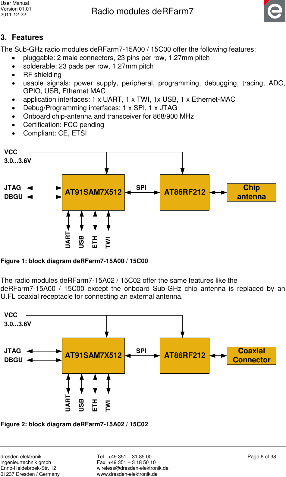
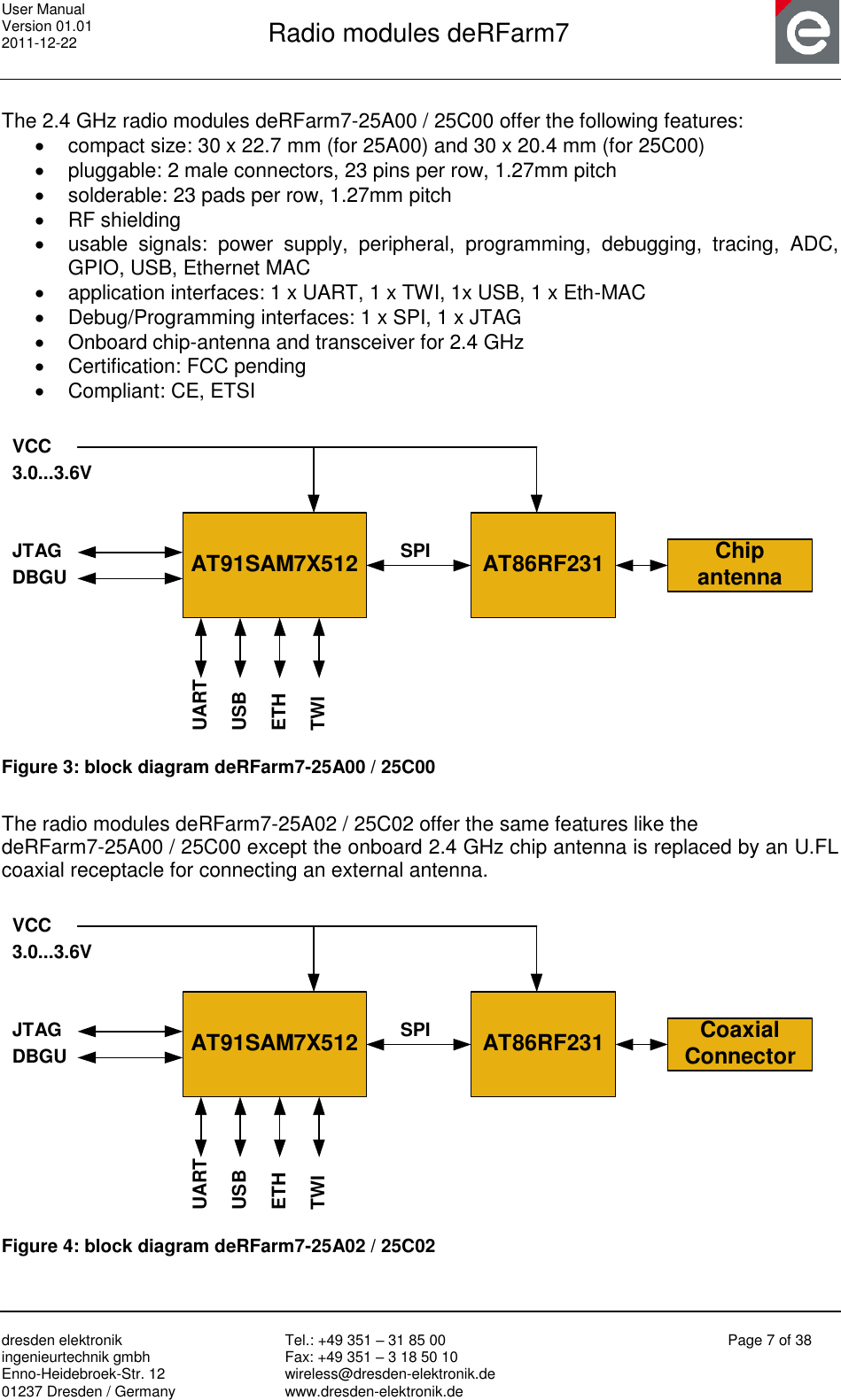
dresden elektronik ingenieurtechnik ARM725A00 2.4GHZ 802.15.4 radio module User Manual
dresden elektronik ingenieurtechnik gmbh 2.4GHZ 802.15.4 radio module
UserManual.wiki
>
dresden elektronik ingenieurtechnik
>
ARM725A00 User Manual
User Manual
Navigation menu
Upload a User Manual
Namespaces
Wiki Guide
HTML
PDF
Info
Views
User Manual
Discussion / Help
Navigation
![User Manual Version 01.01 2011-12-22 Radio modules deRFarm7 dresden elektronik ingenieurtechnik gmbh Enno-Heidebroek-Str. 12 01237 Dresden / Germany Tel.: +49 351 – 31 85 00 Fax: +49 351 – 3 18 50 10 wireless@dresden-elektronik.de www.dresden-elektronik.de Page 4 of 38 Abbreviations Abbreviation Description ADC Analog to Digital Converter BOD Brownout-Detection CE Consumer Electronics DAC Digital to Analog Converter DBGU Debug Unit ETH Ethernet, family of frame-based computer networking technologies for local area networks (LAN). EMAC Ethernet Media Access Controller ETSI European Telecommunications Standards Institute FCC Federal Communications Commission GPIO Generals Purpose Input Output ISM Industrial, Scientific and Medical frequency band JTAG Joint Test Action Group ISP In-System-Programming MAC Medium (Media) Access Control MCU, µC Microcontroller Unit PCB Printed Circuit Board PCBA Printed Circuit Board Assembled PWM Pulse Width Modulation RF Radio Frequency RMII Reduced Media Independent Interface SPI Serial Peripheral Interface TWI Two-Wire Serial Interface U[S]ART Universal [Synchronuous/]Asynchronous Receiver Transmitter USB Universal Serial Bus](https://usermanual.wiki/dresden-elektronik-ingenieurtechnik/ARM725A00/User-Guide-1609600-Page-4.png)
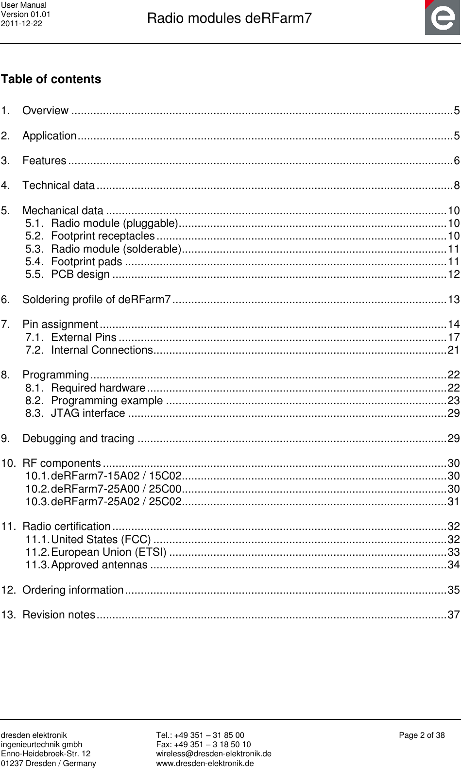
![User Manual Version 01.01 2011-12-22 Radio modules deRFarm7 dresden elektronik ingenieurtechnik gmbh Enno-Heidebroek-Str. 12 01237 Dresden / Germany Tel.: +49 351 – 31 85 00 Fax: +49 351 – 3 18 50 10 wireless@dresden-elektronik.de www.dresden-elektronik.de Page 13 of 38 6. Soldering profile of deRFarm7 Table gives the soldering profile for the radio modules. Table 5: Soldering Profile Profile Feature Values Average-Ramp-up Rate (217°C to Peak) 3°C/sec max. Preheat Temperature 175°C ±25°C 120 sec. max Temperature Maintained Above 217°C 60 sec. Time within 5°C of Actual Peak Temperature 20 sec. to 40 sec. Peak Temperature Range 260° Ramp-down Rate 6°C/sec max. Time 25°C to Peak Temperature 8 min. max. Figure 9 shows a recorded soldering profile for a radio module. The blue colored line illus-trates a temperature sensor placed next to the soldering-contacts of the radio module. The pink line shows the set temperatures depending on the zone within the reflow soldering ma-chine. 406080100120140160180200220240260280020406080100120140160180200220240260280300320340360t [s]T [°C]Measured Temp. Zone Temp. Figure 9: Recorded soldering profile A solder process without supply of nitrogen causes a discoloration of the metal RF-shielding.](https://usermanual.wiki/dresden-elektronik-ingenieurtechnik/ARM725A00/User-Guide-1609600-Page-13.png)
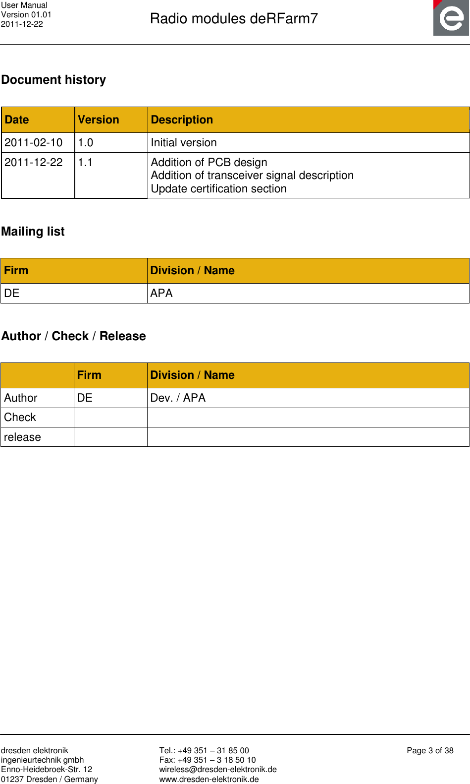
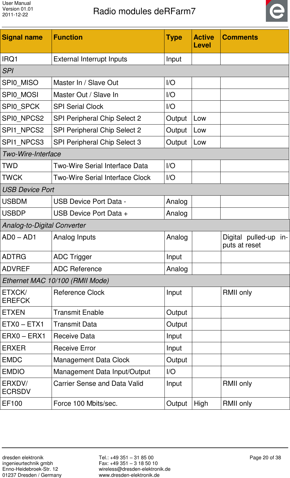
![User Manual Version 01.01 2011-12-22 Radio modules deRFarm7 dresden elektronik ingenieurtechnik gmbh Enno-Heidebroek-Str. 12 01237 Dresden / Germany Tel.: +49 351 – 31 85 00 Fax: +49 351 – 3 18 50 10 wireless@dresden-elektronik.de www.dresden-elektronik.de Page 19 of 38 Table 8: Signal description list Signal name Function Type Active Level Comments Power VCC Voltage Regulator Power Supply Input Power 3.0V to 3.6V GND Ground JTAG TCK Test Clock Input On-board Pull-up TDI Test Data In Input On-board Pull-up TDO Test Data Out Output TMS Test Mode Select Input On-board Pull-up JTAGSEL JTAG Selection Input On-Board Pull-down Debug Unit DRXD Debug Receive Data Input DTXD Debug Transmit Data Output Reset RSTN Microcontroller Reset I/O Low Pull-Up resistor Clocks, Oscillators PCK0 - PCK3 Programmable Clock Output Output U[S]ART TXD0 Transmit Data I/O RXD0 Receive Data Input RTS0 Request To Send Output CTS0 Clear To Send Input DTR1 Data Terminal Ready Output RI1 Ring Indicator Input Timer/Counter and PWM Controller TIOA1 – 2 I/O Line A I/O TIOB1 – 2 I/O Line B I/O TCLK1 External Clock Inputs Input PWM Controller PWM0 - 2 PWM Channels Output Interrupt](https://usermanual.wiki/dresden-elektronik-ingenieurtechnik/ARM725A00/User-Guide-1609600-Page-19.png)
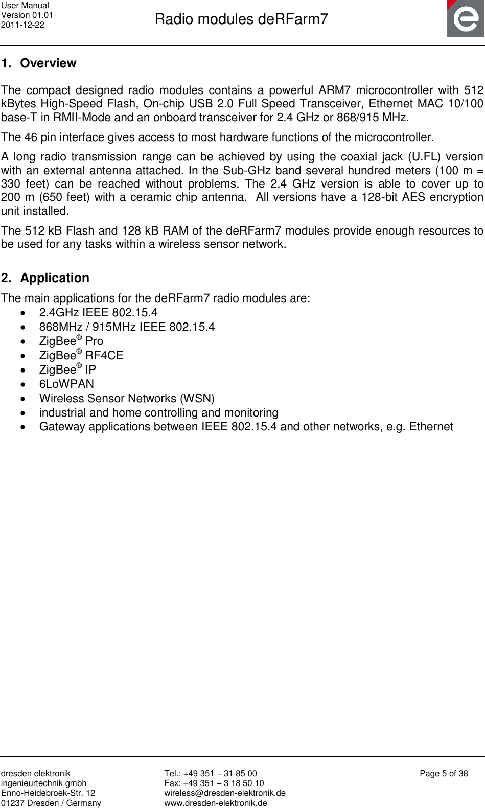
![User Manual Version 01.01 2011-12-22 Radio modules deRFarm7 dresden elektronik ingenieurtechnik gmbh Enno-Heidebroek-Str. 12 01237 Dresden / Germany Tel.: +49 351 – 31 85 00 Fax: +49 351 – 3 18 50 10 wireless@dresden-elektronik.de www.dresden-elektronik.de Page 34 of 38 If the CE marking is reduced or enlarged, the proportions given in the above graduat-ed drawing must be respected. The CE marking must have a height of at least 5mm except where this is not possible on account of the nature of the apparatus The CE marking must be affixed visibly, legibly, and indelibly. More detailed information about CE marking requirements you can find at "DIRECTIVE 1999/5/EC OF THE EUROPEAN PARLIAMENT AND OF THE COUNCIL" on 9 March 1999 at section 12. 11.3. Approved antennas The deRFarm7-25A00 has an integrated chip antenna. The design is fully compliant with all regulations. The deRFarm7-15A02 has been tested and approved for use with the antenna listed below. The module may be integrated with other custom design antennas which OEM installer must authorize with respective regulatory agencies. The used antenna was connected to the radio module with a 15cm “U.FL-to-SMA pigtail”. Table 10: Approved antenna(s) and accessory Approved antenna(s) and accessory Part number Description Manufacturer Gain [dBi] Min. Separation [cm] ANT-916-CW-HWR-RPS ½ wave whip antenna (915 MHz) with RP-SMA-Connector Antenna Factor 0 20 PSKN3-2400RS ½ wave whip antenna (2450 MHz) with RP-SMA-Connector Mobile Mark 2.3 20 BN-032125 U.FL to RP-SMA pigtail, 15 cm Hirose / Profineon -0,35](https://usermanual.wiki/dresden-elektronik-ingenieurtechnik/ARM725A00/User-Guide-1609600-Page-34.png)