eco power design ECOEWI 2.4 GHz Transceiver User Manual EWI Module
eco power design llc 2.4 GHz Transceiver EWI Module
Contents
- 1. Addentum
- 2. Manual r1
Manual r1

EcoPowerDesign
EWI
Usermanual
2.4GHzIEEEStd.802.15.4™
TransceiverModule
2.4GHzIEEEStd.802.15.4TM5dBmRFTransceiverModule
APPLICATIONS
• IEEE 802.15.4 systems
• ZigBee® systems
• Industrial monitoring and control
• Home and building automation
• Automatic Meter Reading
• Low-power wireless sensor networks
• Set-top boxes and remote controls
• Consumer electronics
KEY FEATURES
• State-of-the-art selectivity/co-existence
• Adjacent channel rejection: 49 dB
• Alternate channel rejection: 54 dB
• Excellent link budget (103dB)
• 400 m Line-of-sight range
• Extended temp range (-40 to +125°C)
• Wide supply range: 1.8 V – 3.8 V
• Extensive IEEE 802.15.4 MAC hardware
support to offload the microcontroller
• AES-128 security module
• CC2420 interface compatibility mode
Low Power
• RX (receiving frame, -50 dBm) 18.5 mA
• TX 33.6 mA @ +5 dBm
• TX 25.8 mA @ 0 dBm
• <1µA in power down
Radio
• IEEE 802.15.4 compliant DSSS
baseband modem with 250 kbps data
rate
• Excellent receiver sensitivity (-98 dBm)
• Programmable output power up to +5
dBm
• RF frequency range 2394-2507 MHz
• Suitable for systems targeting
compliance with US radio frequency
regulations,
• FCC CFR47 Part 15
Microcontroller Support
• Digital RSSI/LQI support
• Automatic clear channel assessment for
CSMA/CA
• Automatic CRC
• 768 bytes RAM for flexible buffering and
security processing
• Fully supported MAC security
• 4 wire SPI
• Interrupt generator
• Frame filtering and processing engine
• Random number generator
FIGURE1:PinDiagram
GND J2‐6
RESET
ˉˉˉˉˉˉˉˉˉˉˉ J2‐5
ENABLE J2‐4
INT J2‐3
SI J2‐2
SCK J2‐1
J1‐1 GND
J1‐2 GND
J1‐3 3V3
J1‐4 NC
J1‐5 CS
ˉˉˉ
J1‐6 SO
ANT

Table of Contents
1.0DEVICEOVERVIEW4
2.0CIRCUITDESCRIPTION8
3.0REGULATORYAPPROVAL12
4.0ELECTRICALCHARACTERISTICS14
1.0 Device Overview
TheEWImoduleisa2.4GHzIEEEStd.
802.15.4™compliant,surfacemount
modulewithintegratedcrystal,
internalvoltageregulator,matching
circuitry,andamonopole“whip”
antenna.TheEWImoduleoperatesin
thenon‐licensed2.4GHzfrequency
band.Theintegratedmoduledesign
freestheintegratorfromextensiveRF
andantennadesign,andregulatory
compliancetesting,allowingquicker
timetomarket.
TheEWImodulehasreceived
regulatoryapprovalsformodular
devicesintheUnitedStates(FCC).
Modularapprovalremovestheneed
forexpensiveRFandantennadesign,
andallowstheendusertoplacethe
EWImoduleinsideafinishedproduct
andnotrequireregulatorytestingfor
anintentionalradiator(RF
transmitter).
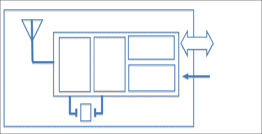
FIGURE11:EWIblockdiagram
EWIIEEEStd.802.15.4™Module
1.1 Interface Description
Figure1‐1showsasimplifiedblock
diagramoftheEWImodule.The
moduleisbasedontheTexas
InstrumentCC2520IEEE802.15.4TM
2.4GHzRFTransceiverIC.The
moduleinterfacestomanypopular
microcontrollersviaa4‐wireserial
SPIinterface,interrupt,enable,Reset,
powerandground,asshowninFigure
1‐2.Table1‐1providesthepin
descriptions.
DatacommunicationswiththeEWI
modulearedocumentedinthe
“CC2520DATASHEET2.4GHZIEEE
802.15.4/ZIGBEE®RF
TRANSCEIVER”(SWRS068
DECEMBER2007).Refertothe
CC2520DataSheetforspecificserial
interfaceprotocolandregister
definitions.
CC2520
Monopole
“whip”
Antenna
Interface Digital
I/O
SPI
Power
32MHz
Crystal
Power
Mgmnt
MAC
Phy
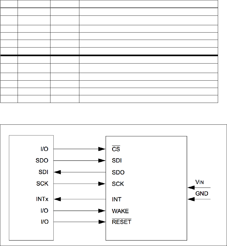
TABLE11:PinDescription
PinSymbolTypeDescription
J2‐6 GND Power Ground
J2‐5 RESET
ˉˉˉˉˉˉˉˉˉˉˉ DI GlobalhardwareResetpin
J2‐4 ENABLE DI Externalwake‐uptrigger
J2‐3 INT DO Interruptpintomicrocontroller
J2‐2 SI DI Serialinterfacedatainput
J2‐1 SCK DI Serialinterfaceclock
J1‐6 SO DO SerialinterfacedataoutputfromCC2520
J1‐5 CS
ˉˉˉ DI Serialinterfaceenable
J1‐4 NC ‐‐ Noconnection
J1‐3 3V3 Power Powersupply
J1‐2 GND Ground Ground
J1‐1 GND Ground Ground
Legend:Pintypeabbreviation:D=Digital,I=Input,O=Output
FIGURE12:MicrocontrollertoEWIModuleInterface
MicrocontrollerCC2520
1.2 Mounting Details
TheEWIisasurfacemountablemodule.
ModuledimensionsareshowninFigure1‐
3.ThemodulePrintedCircuitBoard(PCB)
is0.032"thickwith0.1inconnectionpins
asshowninfig1‐3.Figure1‐4isa
recommendedhostPCBfootprintforthe
EWI.
TheEWIhasamonopole“whip”antenna.
Forthebestperformance,followthe
mountingdetailsshowninFigure1‐5.Itis
recommendedthatthemodulebe
mountedwithnometallicstructuresin
theareamarkedin
fig1‐5
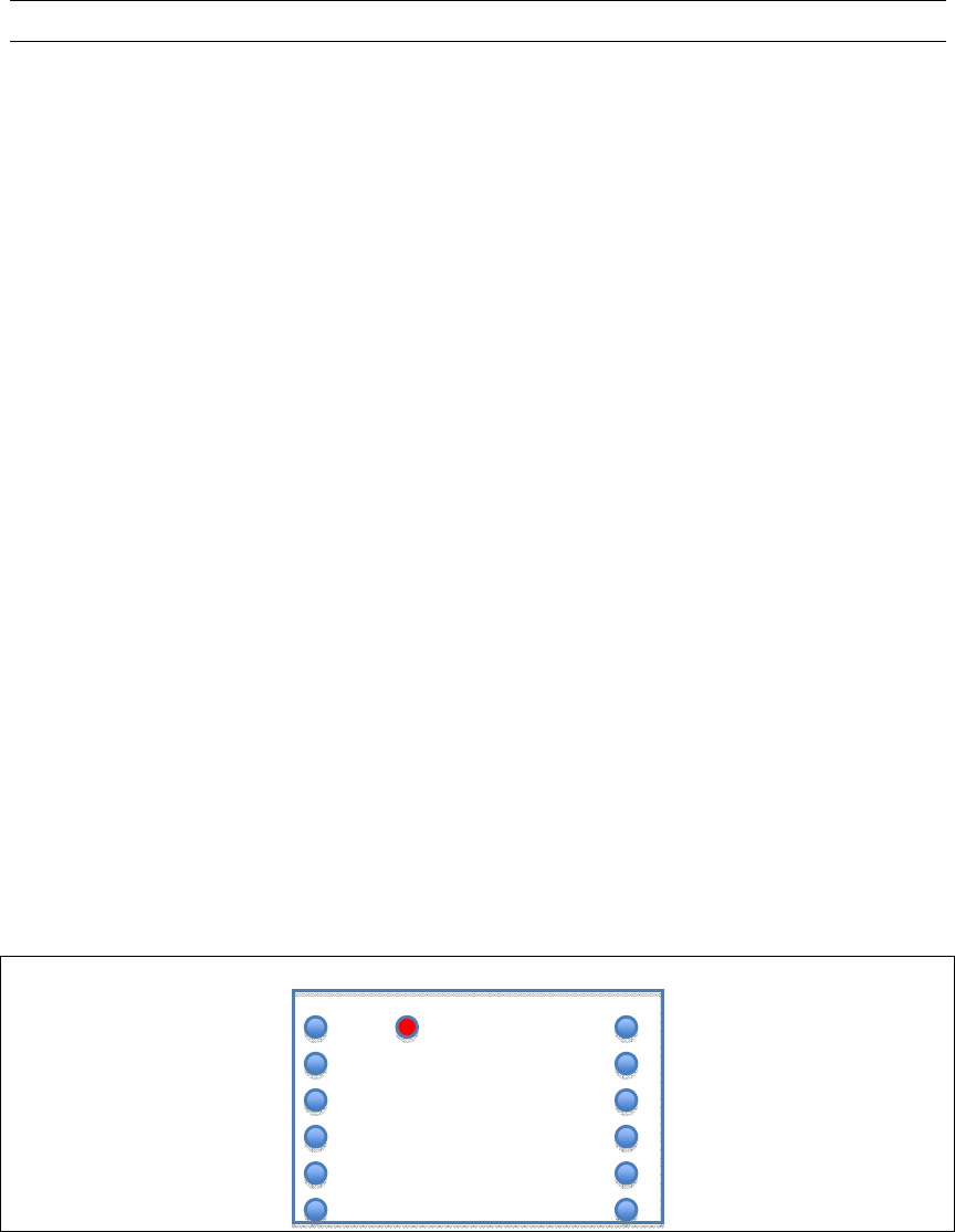
FIGURE13:ModuleDetails
FIGURE14:RecommendedPCB
Footprint
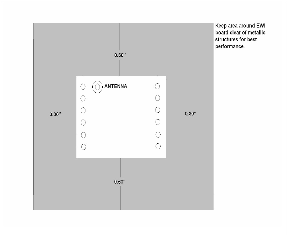
FIGURE15:MountingDetails
2.0 Circuit Description
TheEWIisacomplete2.4GHzIEEE
Std.802.15.4™compliantsurface
mountmodulewithintegratedcrystal,
internalvoltageregulator,matching
circuitry,andamonopole“whip”
antenna.TheEWImoduleinterfaces
tomanypopularmicrocontrollersvia
a4‐wireserialSPIinterface,interrupt,
wake,Reset,powerandground.Data
communicationswiththeEWImodule
aredocumentedinthe“CC2520
DATASHEET2.4GHZIEEE
802.15.4/ZIGBEE®RF
TRANSCEIVER”(SWRS068
DECEMBER2007).Refertothe
CC2520DataSheetforspecificserial
interfaceprotocolandregister
definitions.
2.1 Schematic
Aschematicdiagramofthemoduleis
showninFigure2‐1andtheBillof
Materials(BOM)isshowninTable2‐1.
TheEWImoduleisbasedontheTexas
InstrumentsCC2520IEEE802.15.4™
2.4GHzRFTransceiverIC(U1).The
serialI/O(SCK,SI,SOandCS),RESET,
ENABLEandINTpinsarebroughtout
tothemodulepins.
Crystal,X1,isa32MHzresonatorwith
afrequencytoleranceof±10ppm@
25°CtomeettheIEEEStd.802.15.4
symbolratetoleranceof±40ppm.
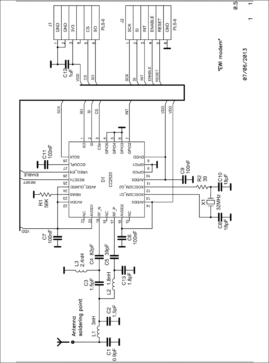
FIGURE21:EWISchematic

TABLE21:EWIBillOfMaterial
RefDescription
Manufacturer
(alt.Manuf.)
PartNumber
(alt.Part.No.)
C1 Capacitor04020.9pFNP0
JohansonTechnology
(Murata)
500R07S0R9BV4S
(GJM1555C1HR90BB01D)
C2 Capacitor04021.5pFNP0
JohansonTechnology
(Murata)
500R07S1R5BV4S
(GJM1555C1H1R5CB01D)
C12 Capacitor04021uFX5R Murata GRM155R60J105KE19
C3 Capacitor04021.5pFNP0 Murata GRM1555C1H1R5CZ01
C13 Capacitor04021.8pFNP0 Murata GRM1555C1H1R8CZ01
C8 Capacitor040215pFNP0 Murata GRM1555C1H150JZ01
C10 Capacitor040215pFNP0 Murata GRM1555C1H150JZ01
C5 Capacitor040239pFNP0 Murata GRM1555C1H390JZ01
C4 Capacitor040282pFNP0 Murata GRM1555C1H820JZ01
C6 Capacitor0402100nFX5R Murata GRM155R61A104KA01
C7 Capacitor0402100nFX5R Murata GRM155R61A104KA01
C9 Capacitor0402100nFX5R Murata GRM155R61A104KA01
C11 Capacitor0402100nFX5R Murata GRM155R61A104KA01
J1
ConnectorPLS‐6,6pin
2.54mmpitch
J2
ConnectorPLS‐6,6pin
2.54mmpitch
D1 TransceiverIEEE802.15.4 TI CC2520RHDT
L1 Inductor04023nH
JohansonTechnology
(Murata)
L‐07C3N0SV6S
(LQG15HN3N0S02D)
L2 Inductor04021.8nH
JohansonTechnology
(Murata)
L‐07C1N8SV6S
(LQG15HN1N8S02D)
L3 Inductor04022.4nH
JohansonTechnology
(Murata)
L‐07C2N4SV6S
(LQG15HN2N4S02D)
R2 Resistor0402395% any
R1 Resistor040256k1% any
X1
32MHzresonator,8pF,80
Ohm,10ppm(25C),
15ppm
(temperaturerange),
‐40...+85C,3.2x2.5mm SJK
SJK‐7U‐32.000‐08‐10‐60‐
C‐15
8pF,10ppm(25C),
‐40...+85C,3.2x2.5mm PDI C332000XFAD08XX
8pF,50ppm(25C),
‐40...+125C,3.2x2.5mm PDI C332000XFCS08RX
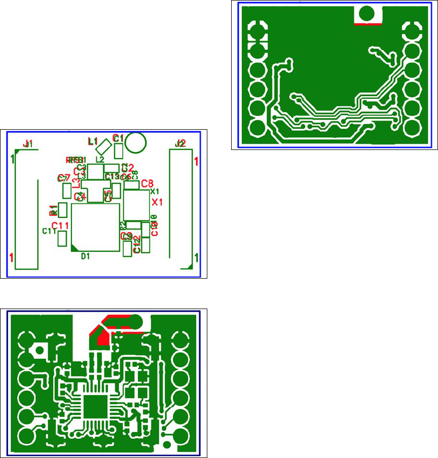
2.2 Printed Circuit Board
TheMRF24J40MBmoduleprinted
circuitboardisconstructedwithFR4
material,fourlayersand0.032inches
thick.ThelayersareshowninFigure
2‐2throughFigure2‐6.Thestackup
ofthePCBisshowninFigure2‐7.
FIGURE22:TopSilkScreen
FIGURE23:TopCopper
FIGURE 2-4: Bottom Copper
2.3 Monopole “whip” Antenna
TheEWIhasamonopole“whip”
antenna.Thegroundandpower
planesunderthecomponentsserveas
acounterpoisetothe“whip”antenna.
Additionalgroundplaneonthehost
PCBwillsubstantiallyenhancethe
performanceofthemodule.Forbest
performance,placethemoduleonthe
hostPCBfollowingthe
recommendationsinSection1.2
“MountingDetails”.
Thedesigngoalwastocreatea
compact,low‐costantennawiththe
bestradiationpattern.Figure2‐9
showsthesimulationdrawingand
Figure2‐10andFigure2‐11showthe
2Dand3Dradiationpatterns,
respectively.Asshownbythe
radiationpatterns,theperformanceof
theantennaisdependantuponthe
orientationofthemodule.Figure2‐12
showstheimpedancesimulationand
Figure2‐13showstheSWR
simulation.Thediscretematching
circuitrymatchestheimpedanceof
theantennawiththeCC2520
transceiverIC.

3.0 Regulatory Approval
TheEWImodulehasreceived
regulatoryapprovalsformodular
devicesintheUnitedStates.Modular
approvalallowstheendusertoplace
theEWImoduleinsideafinished
productandnotrequireregulatory
testingforanintentionalradiator(RF
transmitter),providednochangesor
modificationsaremadetothemodule
circuitry.Changesormodifications
couldvoidtheuser’sauthorityto
operatetheequipment.Theenduser
mustcomplywithallofthe
instructionsprovidedbytheGrantee,
whichindicateinstallationand/or
operatingconditionsnecessaryfor
compliance.
Theintegratormaystillberesponsible
fortestingtheendproductforany
additionalcompliancerequirements
requiredwiththismodule,installed
(forexample:digitaldeviceemission,
PCperipheralrequirements,etc.)in
thespecificcountrythattheend
devicewillbemarketed.
AnnexFoftheIEEEStd.802.15.4
documenthasagoodsummaryof
regulatoryrequirementsinvarious
countriesconcerningIEEEStd.
802.15.4devices.Thestandardcanbe
downloadedfromtheIEEEStandards
webpage:
http://standards.ieee.org/getieee802
/802.15.html.
Refertothespecificcountryradio
regulationsfordetailsonregulatory
compliance.
3.1 United States
TheEWImodulehasreceivedFederaö
CommunicationsCommission(FCC)
CFR47Telecommunications,Part15
SubpartC“IntentionalRadiators”
15.247andmodularapprovalin
accordancewithFCCPublicNoticeDA
00‐1407Released:June26,2000,Part
15UnlicensedModularTransmitter
Approval.TheEWImodulecanbe
integratedintoafinishedproduct
withoutobtainingsubsequentand
separateFCCapprovals.
TheEWImodulehasbeenlabeled
withitsownFCCIDnumber,andifthe
FCCIDisnotvisiblewhenthemodule
isinstalledinsideanotherdevice,then
theoutsideofthefinishedproduct
intowhichthemoduleisinstalled
mustalsodisplayalabelreferringto
theenclosedmodule.Thisexterior
labelcanusewordingsuchasthe
following:
ContainsTransmitterModuleFCCID:
OA3EWI
‐or‐
ContainsFCCID:OA3EWI
ThisdevicecomplieswithPart15of
theFCCRules.Operationissubjectto
thefollowingtwoconditions:(1)this
devicemaynotcauseharmful
interference,and(2)thisdevicemust
acceptanyinterferencereceived,
includinginterferencethatmaycause
undesiredoperation.
Thisequipmenthasbeentestedand
foundtocomplywiththelimitsfora
ClassBdigitaldevice,pursuanttopart
15oftheFCCRules.Theselimitsare
designedtoprovidereasonable
protectionagainstharmful
interferenceinaresidential
installation.Thisequipment
generates,usesandcanradiateradio
frequencyenergy,andifnotinstalled
andusedinaccordancewiththe
instructions,maycauseharmful
interferencetoradiocommunications.
However,thereisnoguaranteethat

interferencewillnotoccurina
particularinstallation.Ifthis
equipmentdoescauseharmful
interferencetoradioortelevision
reception,whichcanbedetermined
byturningtheequipmentoffandon,
theuserisencouragedtotryto
correcttheinterferencebyoneor
moreofthefollowingmeasures:
‐Reorientorrelocatethereceiving
antenna.
‐Increasetheseparationbetweenthe
equipmentandreceiver.
‐Connecttheequipmentintoan
outletonacircuitdifferentfromthat
towhichthereceiverisconnected.
‐Consultthedealeroranexperienced
radio/TVtechnicianforhelp.
3.1.1 EWI Settings
TomeettheFCCrequirements,the
followingsettingsmustbeobserved
bytheintegrator:
•TheEWItransmitpowersetting
(RFCON30x203)cannotexceed‐1.9
dB.
•Onlychannels11through25maybe
selected(RFCON00x200).
3.1.2 RF Exposure
AlltransmittersregulatedbyFCC
mustcomplywithRFexposure
requirements.OETBulletin65
“EvaluatingCompliancewithFCC
GuidelinesforHumanExposureto
RadioFrequencyElectromagnetic
Fields”providesassistancein
determiningwhetherproposedor
existingtransmittingfacilities,
operationsordevicescomplywith
limitsforhumanexposuretoRadio
Frequency(RF)fieldsadoptedbythe
FederalCommunicationsCommission
(FCC).Thebulletinoffersguidelines
andsuggestionsforevaluating
compliance.
Ifappropriate,compliancewith
exposureguidelinesformobileand
unlicenseddevicescanbe
accomplishedbytheuseofwarning
labelsandbyprovidinguserswith
informationconcerningminimum
separationdistancesfrom
transmittingstructuresandproper
installationofantennas.
Thefollowingstatementmustbe
includedasaCAUTIONstatementin
manualsandOEMproductstoalert
usersofFCCRFexposurecompliance:
TosatisfyFCCRFexposure
requirementsformobileandbase
stationtransmissiondevices,a
separationdistanceof20cmormore
shouldbemaintainedbetweenthe
antennaofthisdeviceandpersons
duringoperation.Toensure
compliance,operationatcloserthan
thisdistanceisnotrecommended.
Theantenna(s)usedforthis
transmittermustnotbeco‐locatedor
operatinginconjunctionwithany
otherantennaortransmitter.
IftheEWImoduleisusedinaportable
application(antennaislessthan20
cmfrompersonsduringoperation),
theintegratorisresponsiblefor
performingSpecificAbsorptionRate
(SAR)testinginaccordancewith
FCCrules2.1091.
3.1.3 Helpful Web Sites
FederalCommunicationsCommission
(FCC):http://www.fcc.gov

4.0 Electrical Characteristics
TABLE41:RecommendedOperatingConditions
ParametersMinTypMaxUnits
AmbientOperatingTemperature ‐40 125 °C
SupplyVoltageforRF,AnalogandDigitalCircuits 1.8 3.8 V
SupplyVoltageforDigitalI/O
InputHighVoltage 80% ofVDD
InputLowVoltage 30% ofVDD
TABLE42:CurrentConsumption
TA=25°C,VDD=3.0V,fc=2440MHzifnothingelsestated.AllparametersmeasuredonTexasInstruments’
CC2520EM2.1referencedesignwith50Ωload
Parameter
ConditionMinTypMax
Units
Receive
current
Waitforsync
TA=‐40to125°C,VDD=1.8to3.8V,
fc=2394to2507MHz
Waitforsync,Low‐currentRXsetting
Recevingframe,‐50dBminputlevel
22.324.8
26.3
18.8
18.8
mA
mA
mA
mA
Transmit
current
0dBmsetting
+5dBmsetting
TA=‐40to125°C,VDD=1.8to3.8V,
fc=2394to2507MHz
25.828.8
33.637.2
37.5
mA
mA
mA
ActiveMode
current
XOSCon,digitalregulatoron.
TA=‐40to125°C,VDD=1.8to3.8V,
fc=2394to2507MHz
1.6 1.9
2.6
mA
mA
LPM1current XOSCoff,digitalregulatoron.Stateretention.
TA=‐40to125°C,VDD=1.8to3.8V,
fc=2394to2507MHz
175 250
1000
µA
µA
LPM2current XOSCoff,digitalregulatoroff.Nostateretention.
TA=‐40to125°C,VDD=1.8to3.8V,
fc=2394to2507MHz
30 120
4.5
nA
µA

TABLE43:ReceiverACCharacteristics
TA=25°C,VDD=3.0V,fc=2440MHzifnothingelsestated.AllparametersmeasuredonTexas
Instruments’CC2520EM2.1referencedesignwith50Ωload.
Parameter
ConditionMinTypMax
Units
Receiver
sensitivity
[2]requires‐85dBm
TA=‐40to125°C,VDD=1.8to3.8V,fc=2394to2507
MHz
‐99 ‐98 ‐95
‐88
dBm
Saturation [2]requires‐20dBm6dBm
Interferer
Rejection
Wantedsignal3dBabovethesensitivitylevel,
802.15.4modulated
interfererat802.15.4channels:
±5MHzfromwantedsignal.[2]requires0dB
±10MHzfromwantedsignal.[2]requires30
dB
±20MHzorabove.Wantedsignalat‐82dBm.
49
54
55
dB
dB
dB
Maximum
Spurious
Emission
Conducted
measurementin
a50Ωsingle
endedload.
Complieswith
EN300328,EN
300440class2,
FCCCFR47,Part
15andARIB
STD‐T‐66
30–1000MHz
1–12.75GHz
<‐80
‐56
dBm
dBm
Frequency
error
tolerance
Inputlevelis3dBabovesensitivitylevel. +/‐400 kHz
IIP3 ‐24 dBm
TABLE44:TransmitterACCharacteristics
Parameter
ConditionMinTypMax
Units
Outputpower
Note:toreduce
theoutput
powervariation
over
temperature,it
issuggested
thatdifferent
0dBmsetting
+5dBmsetting
T
A=‐40to85°C,VDD=2.0to3.8V,
f
c=2394to2507MHz
T
A=‐40to85°C,VDD=1.8to3.8V,
‐3 1 5
2 5 7
‐3 8
dBm
dBm
dBm

settingsare
usedat
different
temperatures.
Theon‐chip
temperature
sensorcanbe
usedforthis
purpose.
Pleasesee
section5.11for
more
information.
Largest
spurious
emissionat
maximum
outputpower.
Texas
Instruments
CC2520EM
reference
designcomplies
withEN300
328,EN300
440,FCCCFR47
Part15and
ARIBSTDT‐66.
Transmiton
2480MHz
underFCCat+5
dBmis
supportedby
duty‐cycling,or
byreducing
outputpower.
Thepeak
conducted
spurious
emissionmight
violateETSIand
FCCrestricted
bandlimitsat
frequencies
below1GHz.All
radiated
spurious
emissionsare
withinthe
limitsof
ETSI/FCC/
ARIB.
Applications
thatmustpass
conducted
requirements
aresuggestedto
useasimple50
f
c=2394to2507MHz
T
A=‐40to125°C,VDD=2.0to3.8V,
f
c=2394to2507MHz
T
A=‐40to125°C,VDD=1.8to3.8V,
f
c=2394to2507MHz
25MHz–1GHz(outsiderestrictedbands)
25MHz–1GHz(withinFCCrestrictedbands)
47‐74,87.5‐118,174‐230,470‐862MHz(ETSI
restrictedbands)
1800MHz‐1900MHz(ETSIrestrictedband)
5150MHz‐5300MHz(ETSIrestrictedband)
At2483.5MHzandabove(FCCrestrictedband)
f
c=2480MHz,+5dBm
f
c=2480MHz,0dBm
At2·RFand3·RF(FCCrestrictedband)
‐4 8
‐6 8
‐9 8
‐40
‐53
‐42
‐56
‐54
‐37
‐41
‐54
dBm
dBm
dBm
dBm
dBm
dBm
dBm
dBm
dBm
dBm
dBm

Ωhighpass
filterbetween
matching
networkandRF
connector.
ErrorVector
Magnitude
(EVM)
[2]requiresmax.35%.Measuredasdefinedby[2].
+5dBmsetting.fc=IEEE802.15.4channels
0dBmsetting.fc=IEEE802.15.4channels
6
2
%
%