iRobot ALT240ROB Floor Cleaning, Mopping Robot User Manual Chipset Datasheet
iRobot Corporation Floor Cleaning, Mopping Robot Chipset Datasheet
UserManual.wiki
>
iRobot
>
ALT240ROB User Manual
>
Chipset Datasheet
Contents
1.
Users Manual
2.
Chipset Datasheet
Chipset Datasheet
Navigation menu
Upload a User Manual
Namespaces
Wiki Guide
HTML
PDF
Info
Views
User Manual
Discussion / Help
Navigation
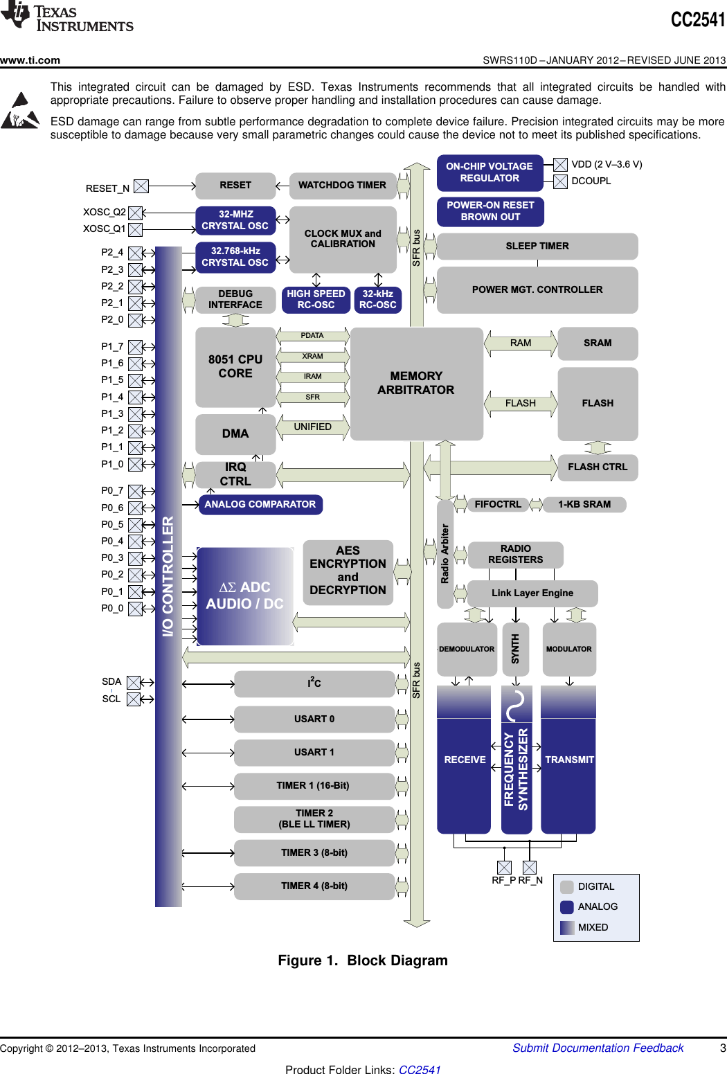
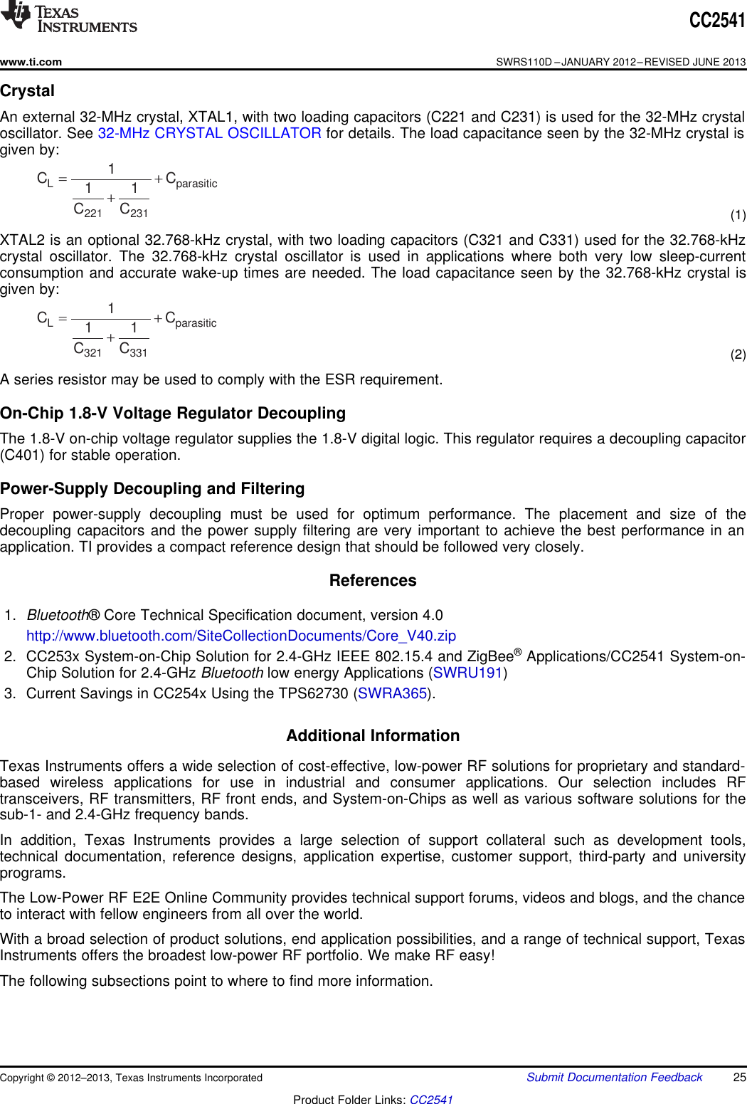
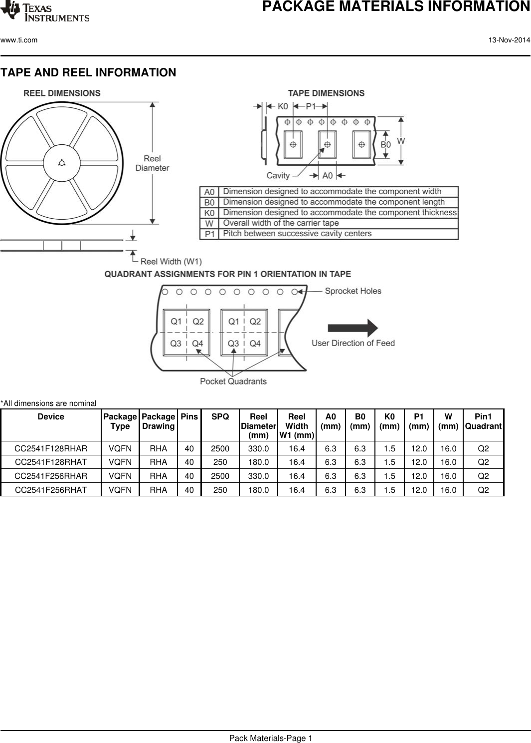
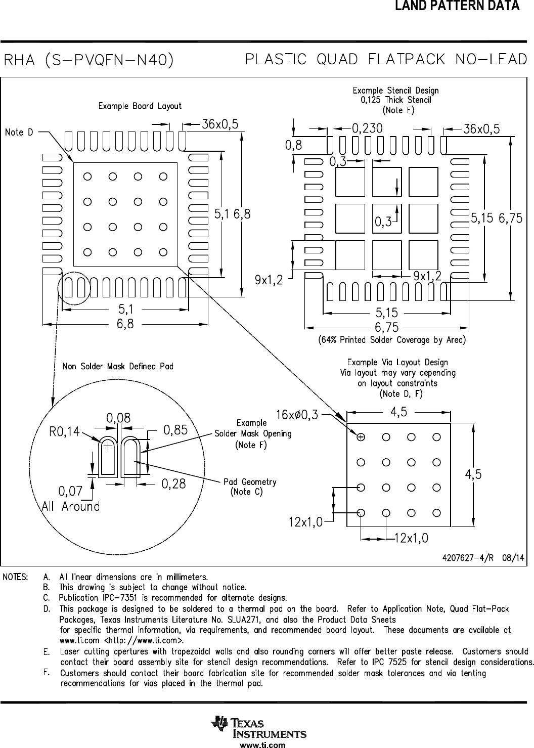
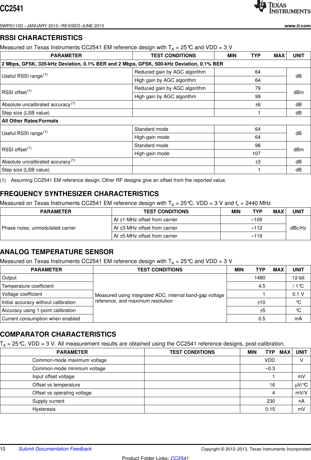
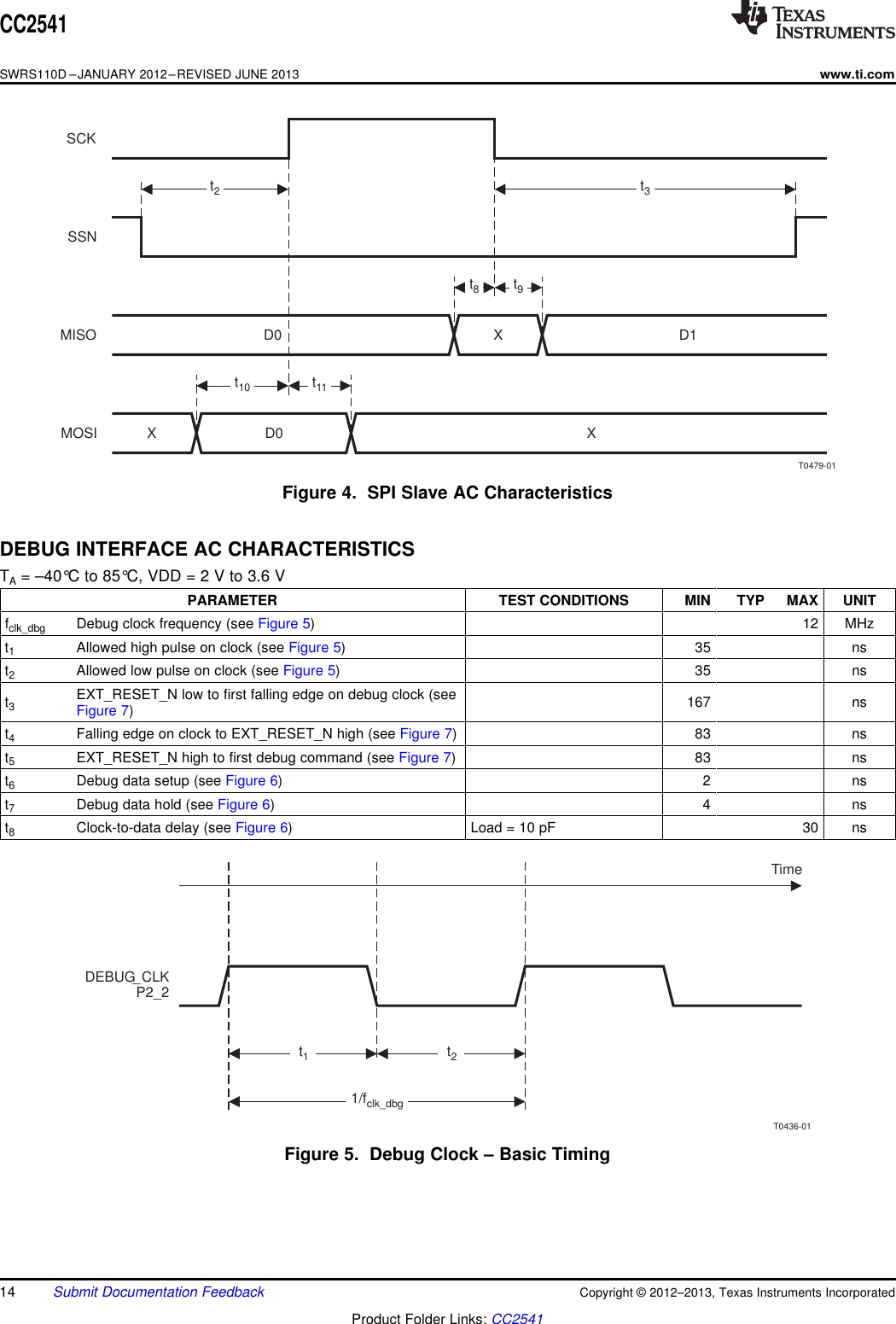
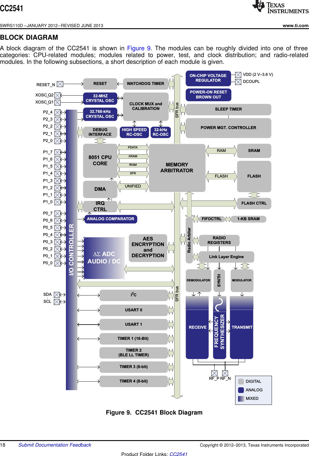
![CC2541SWRS110D –JANUARY 2012–REVISED JUNE 2013www.ti.comRF RECEIVE SECTION (continued)Measured on Texas Instruments CC2541 EM reference design with TA= 25°C, VDD = 3 V, fc= 2440 MHzPARAMETER TEST CONDITIONS MIN TYP MAX UNIT1 Mbps, GFSK, 250-kHz Deviation, Bluetooth low energy Mode, 0.1% BERHigh-gain mode –94Receiver sensitivity(3)(4) dBmStandard mode –88Saturation(4) BER < 0.1% 5 dBmCo-channel rejection(4) Wanted signal –67 dBm –6 dB±1 MHz offset, 0.1% BER, wanted signal –67 dBm –2±2 MHz offset, 0.1% BER, wanted signal –67 dBm 26In-band blocking rejection(4) dB±3 MHz offset, 0.1% BER, wanted signal –67 dBm 34>6 MHz offset, 0.1% BER, wanted signal –67 dBm 33Minimum interferer level < 2 GHz (Wanted signal –67 dBm) –21Out-of-band blocking Minimum interferer level [2 GHz, 3 GHz] (Wanted signal –67 dBm) –25 dBmrejection(4)Minimum interferer level > 3 GHz (Wanted signal –67 dBm) –7Intermodulation(4) Minimum interferer level –36 dBmIncluding both initial tolerance and drift. Sensitivity better than -67dBm,Frequency error tolerance(5) –250 250 kHz250 byte payload. BER 0.1%Symbol rate error Maximum packet length. Sensitivity better than –67 dBm, 250 byte –80 80 ppmtolerance(6) payload. BER 0.1%1 Mbps, GFSK, 160-kHz Deviation, 0.1% BERReceiver sensitivity(7) –91 dBmSaturation BER < 0.1% 0 dBmCo-channel rejection Wanted signal 10 dB above sensitivity level –9 dB±1-MHz offset, 0.1% BER, wanted signal –67 dBm 2±2-MHz offset, 0.1% BER, wanted signal –67 dBm 24In-band blocking rejection dB±3-MHz offset, 0.1% BER, wanted signal -–67 dBm 27>6-MHz offset, 0.1% BER, wanted signal –67 dBm 32Including both initial tolerance and drift. Sensitivity better than –67 dBm,Frequency error tolerance(5) –200 200 kHz250-byte payload. BER 0.1%Symbol rate error Maximum packet length. Sensitivity better than –67 dBm, 250-byte –80 80 ppmtolerance(6) payload. BER 0.1%500 kbps, MSK, 0.1% BERReceiver sensitivity(7) –99 dBmSaturation BER < 0.1% 0 dBmCo-channel rejection Wanted signal –67 dBm –5 dB±1-MHz offset, 0.1% BER, wanted signal –67 dBm 20In-band blocking rejection ±2-MHz offset, 0.1% BER, wanted signal –67 dBm 27 dB>2-MHz offset, 0.1% BER, wanted signal –67 dBm 28Including both initial tolerance and drift. Sensitivity better than –67 dBm,Frequency error tolerance –150 150 kHz250-byte payload. BER 0.1%Maximum packet length. Sensitivity better than –67 dBm, 250-byteSymbol rate error tolerance –80 80 ppmpayload. BER 0.1%(3) The receiver sensitivity setting is programmable using a TI BLE stack vendor-specific API command. The default value is standardmode.(4) Results based on standard-gain mode.(5) Difference between center frequency of the received RF signal and local oscillator frequency(6) Difference between incoming symbol rate and the internally generated symbol rate(7) Results based on high-gain mode.6Submit Documentation Feedback Copyright © 2012–2013, Texas Instruments IncorporatedProduct Folder Links: CC2541](https://usermanual.wiki/iRobot/ALT240ROB.Chipset-Datasheet/User-Guide-2910061-Page-6.png)
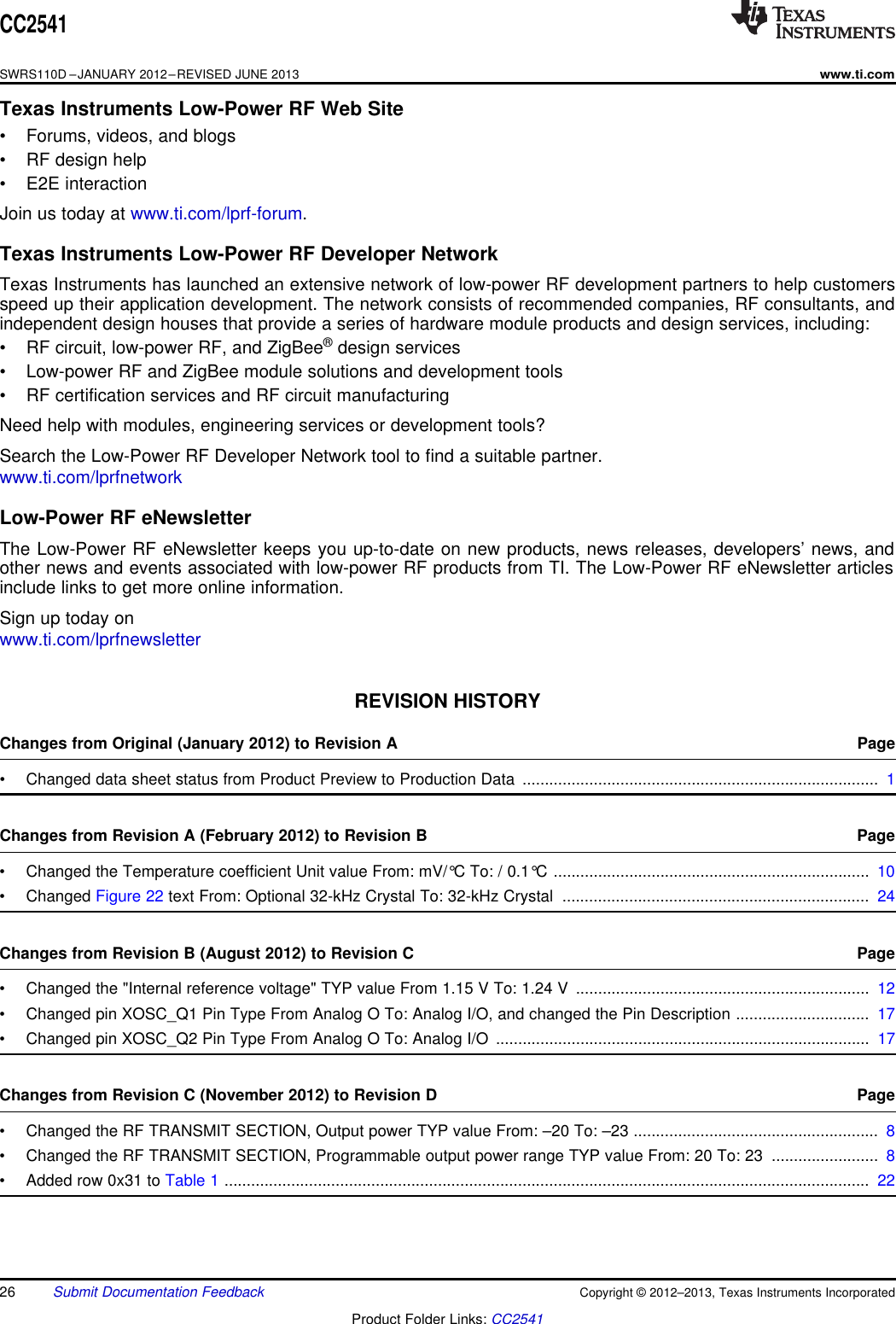
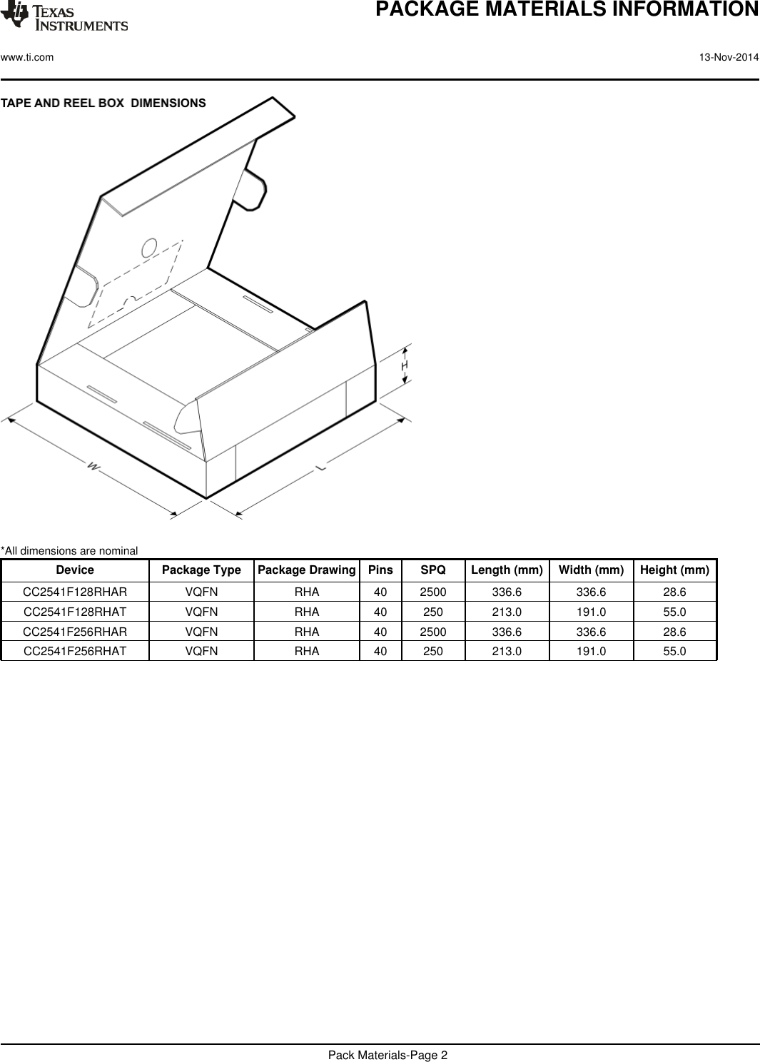
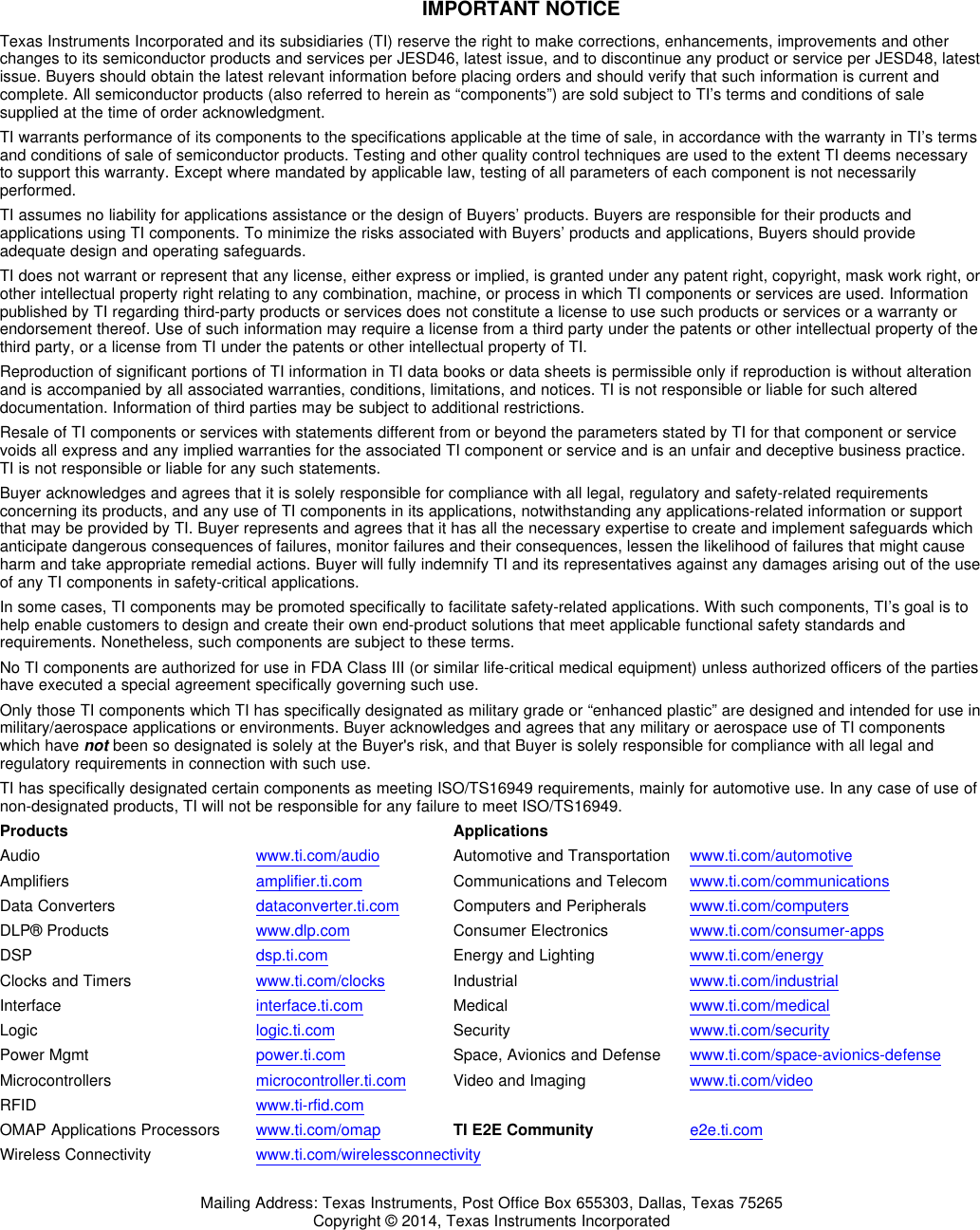
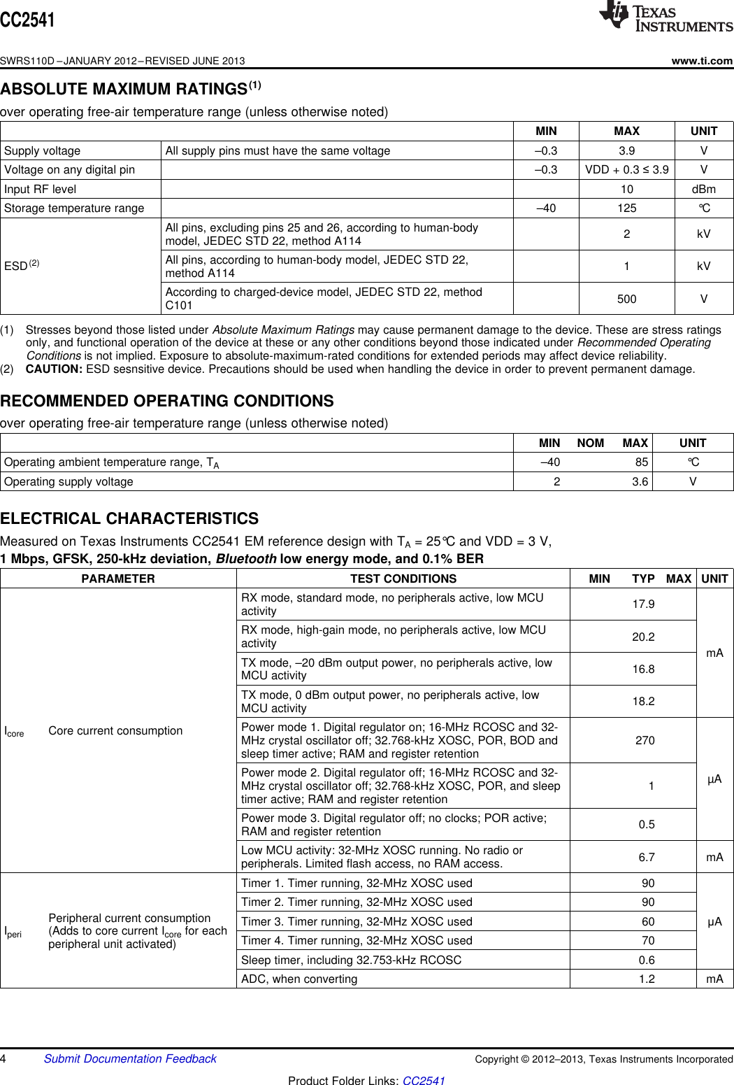
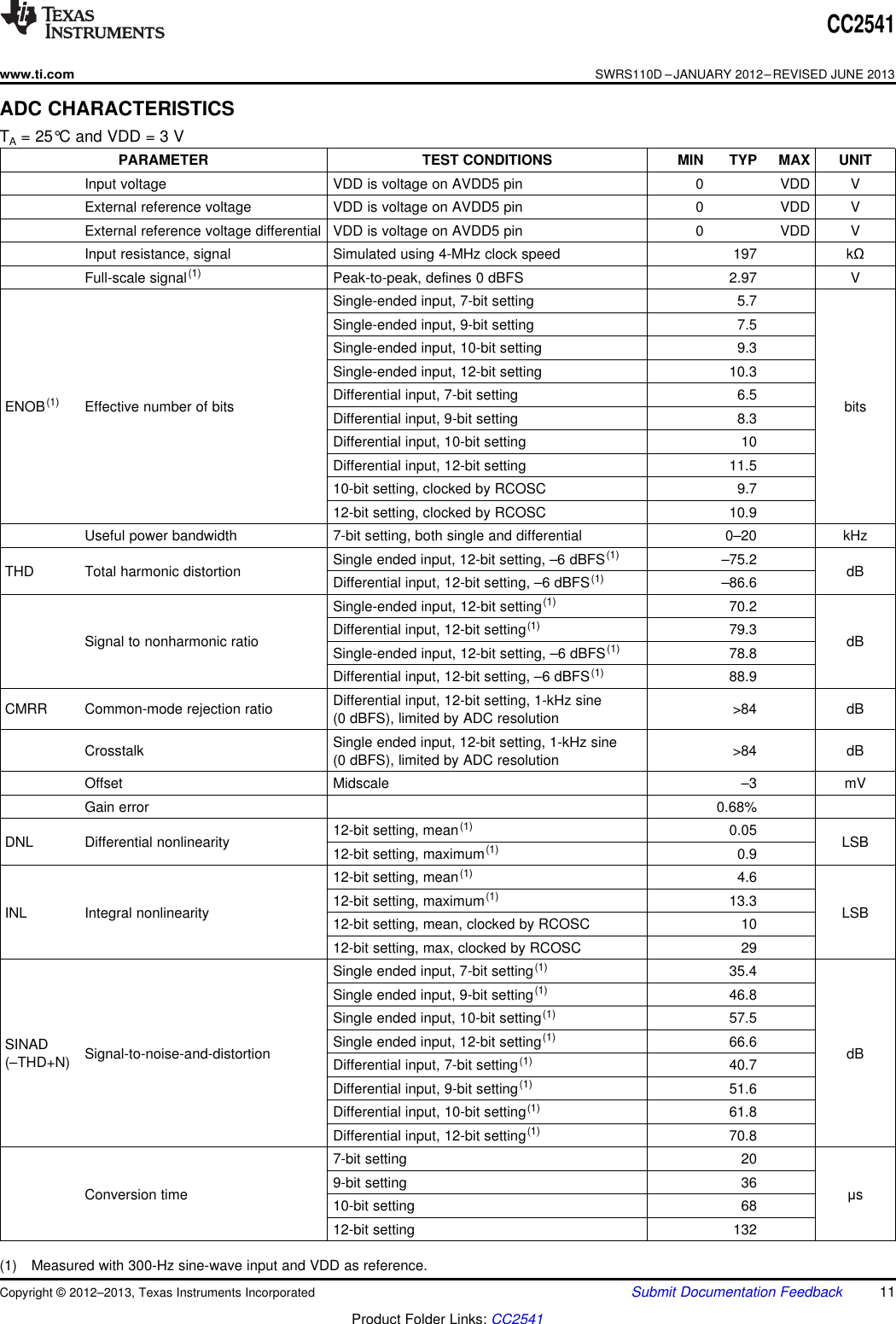
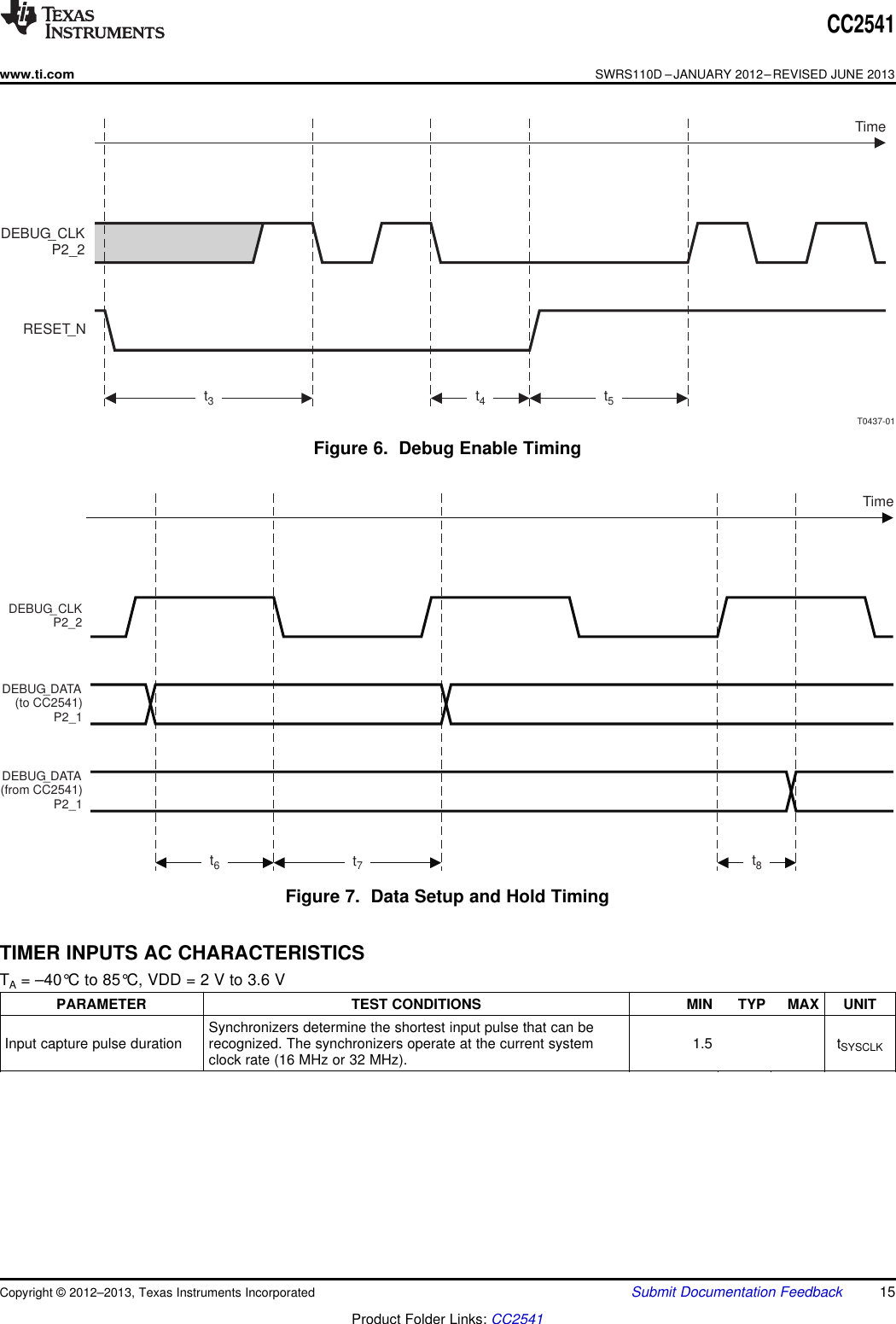
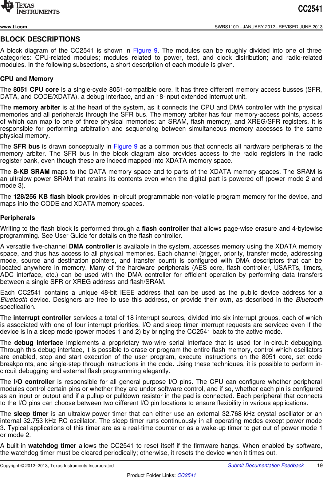
![CC2541SWRS110D –JANUARY 2012–REVISED JUNE 2013www.ti.comRF TRANSMIT SECTIONMeasured on Texas Instruments CC2541 EM reference design with TA= 25°C, VDD = 3 V and fc= 2440 MHzPARAMETER TEST CONDITIONS MIN TYP MAX UNITDelivered to a single-ended 50-Ωload through a balun using 0maximum recommended output power settingOutput power dBmDelivered to a single-ended 50-Ωload through a balun using –23minimum recommended output power settingProgrammable output power Delivered to a single-ended 50-Ωload through a balun using 23 dBrange minimum recommended output power settingf < 1 GHz –52 dBmSpurious emission conducted f > 1 GHz –48 dBmmeasurement Suitable for systems targeting compliance with worldwide radio-frequency regulations ETSI EN 300 328 andEN 300 440 Class 2 (Europe), FCC CFR47 Part 15 (US), and ARIB STD-T66 (Japan)Differential impedance as seen from the RF port (RF_P and RF_N)Optimum load impedance 70 +j30 Ωtoward the antennaDesigns with antenna connectors that require conducted ETSI compliance at 64 MHz should insert an LCresonator in front of the antenna connector. Use a 1.6-nH inductor in parallel with a 1.8-pF capacitor. Connectboth from the signal trace to a good RF ground.CURRENT CONSUMPTION WITH TPS62730Measured on Texas Instruments CC2541 TPA62730 EM reference design with TA= 25°C, VDD = 3 V and fc= 2440 MHz,1 Mbsp, GFSK, 250-kHz deviation, Bluetooth™ low energy Mode, 1% BER(1)PARAMETER TEST CONDITIONS MIN TYP MAX UNITRX mode, standard mode, no peripherals active, low MCU activity, MCU 14.7at 1 MHzRX mode, high-gain mode, no peripherals active, low MCU activity, 16.7MCU at 1 MHzCurrent consumption mATX mode, –20 dBm output power, no peripherals active, low MCU activity, 13.1MCU at 1 MHzTX mode, 0 dBm output power, no peripherals active, low MCU activity, 14.3MCU at 1 MHz(1) 0.1% BER maps to 30.8% PER32-MHz CRYSTAL OSCILLATORMeasured on Texas Instruments CC2541 EM reference design with TA= 25°C and VDD = 3 VPARAMETER TEST CONDITIONS MIN TYP MAX UNITCrystal frequency 32 MHzCrystal frequency accuracy –40 40 ppmrequirement(1)ESR Equivalent series resistance 6 60 ΩC0Crystal shunt capacitance 1 7 pFCLCrystal load capacitance 10 16 pFStart-up time 0.25 msThe crystal oscillator must be in power down for a guardtime before it is used again. This requirement is valid forPower-down guard time 3 msall modes of operation. The need for power-down guardtime can vary with crystal type and load.(1) Including aging and temperature dependency, as specified by [1]8Submit Documentation Feedback Copyright © 2012–2013, Texas Instruments IncorporatedProduct Folder Links: CC2541](https://usermanual.wiki/iRobot/ALT240ROB.Chipset-Datasheet/User-Guide-2910061-Page-8.png)
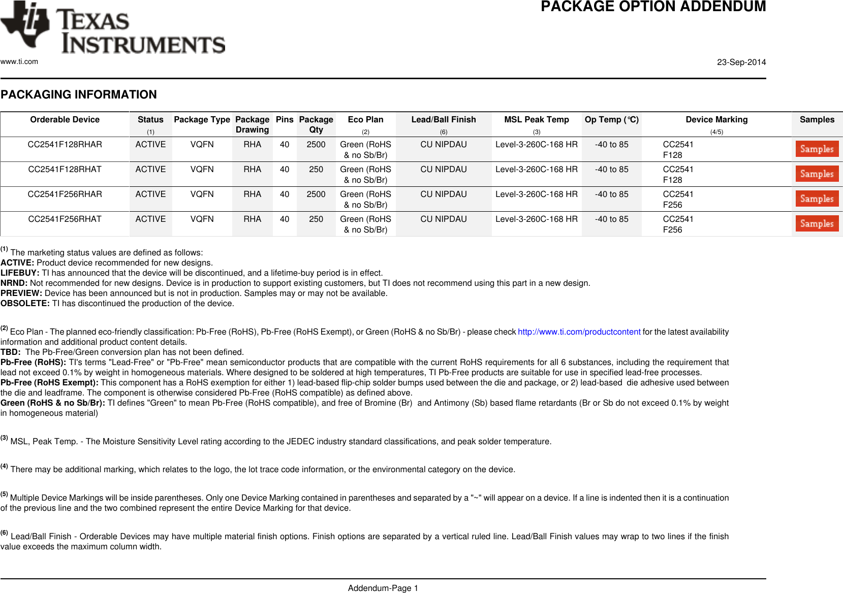
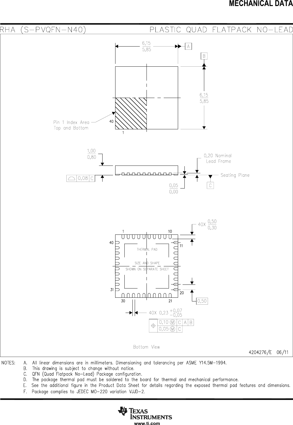
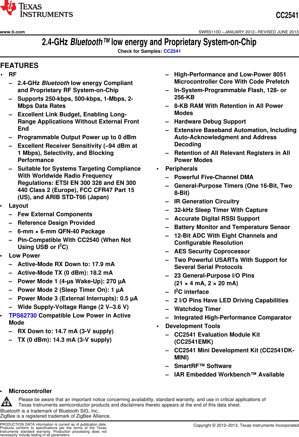
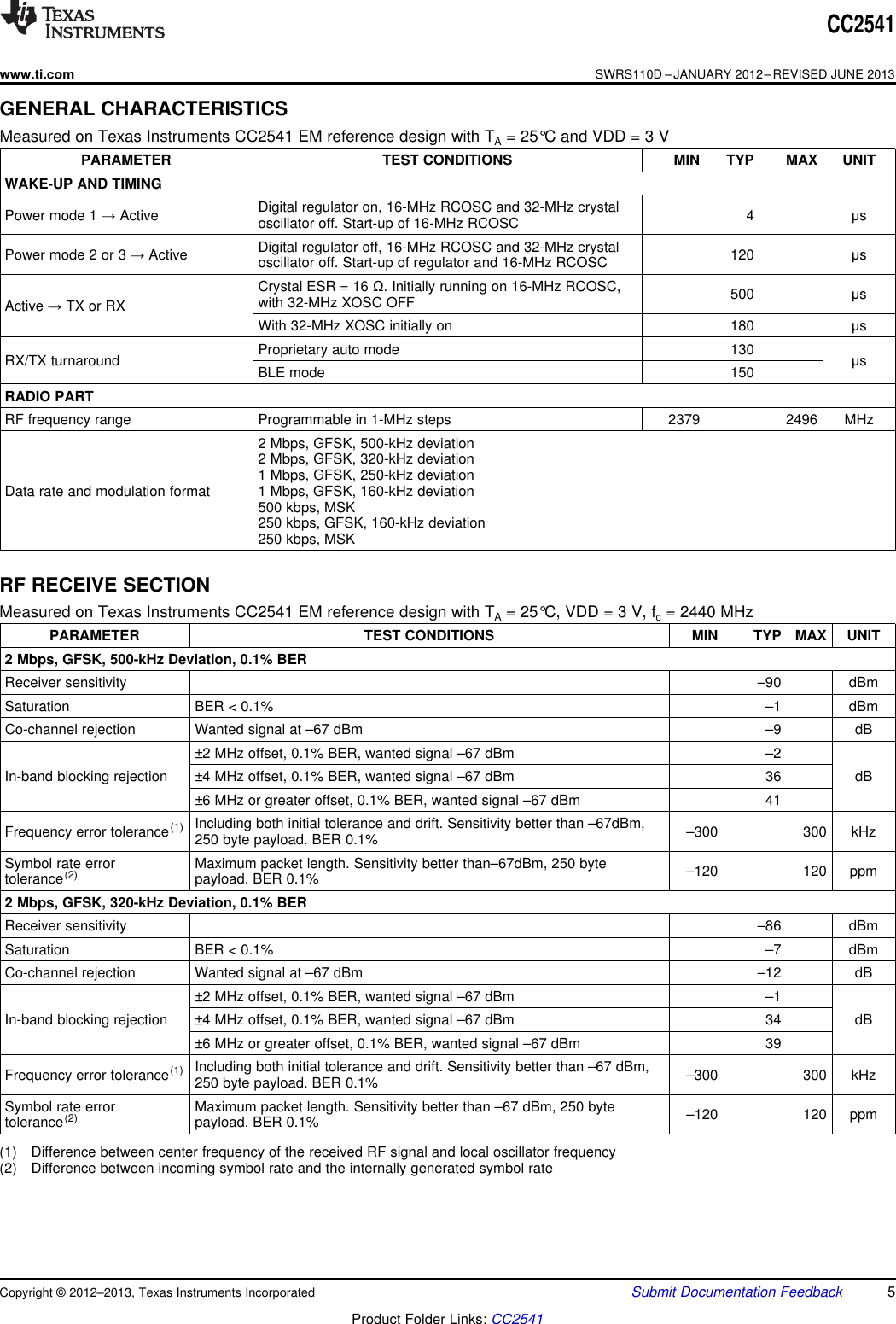
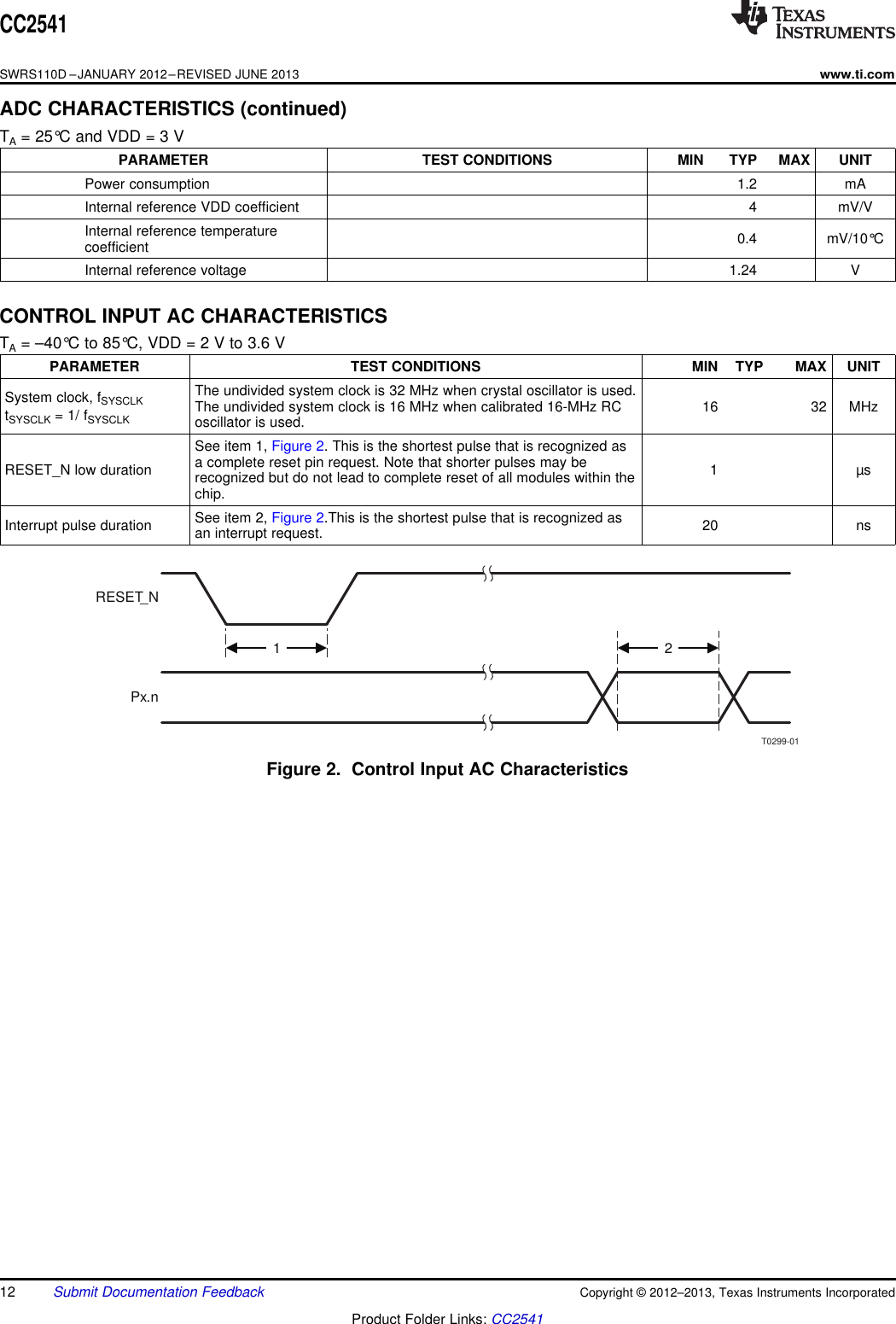
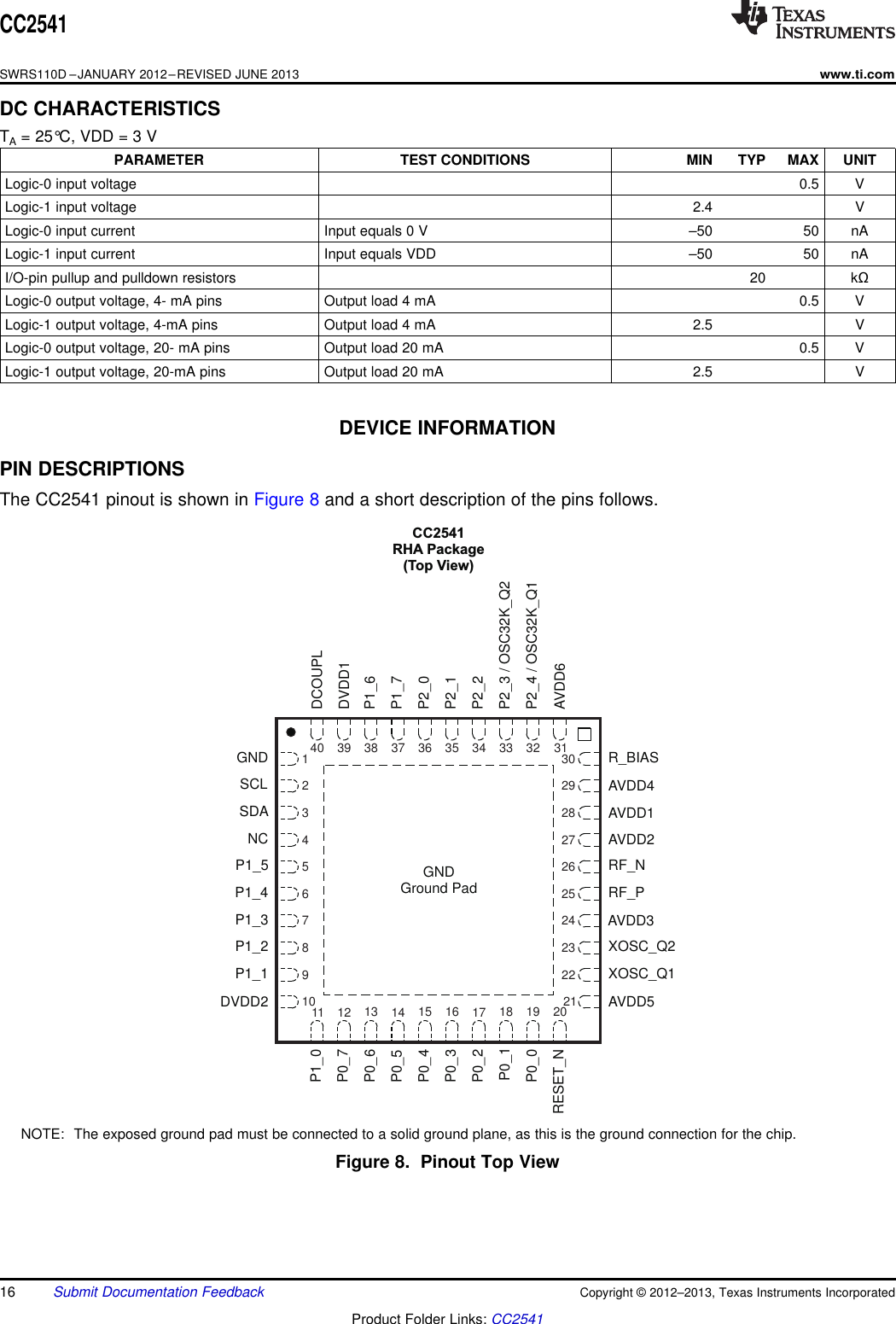
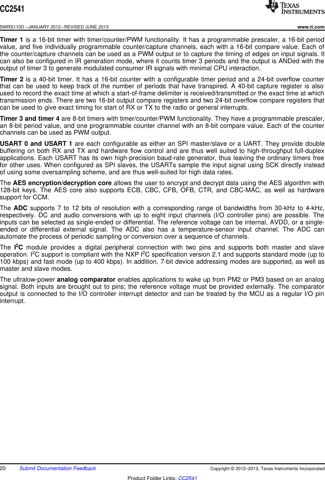
![CC2541www.ti.comSWRS110D –JANUARY 2012–REVISED JUNE 201332.768-kHz CRYSTAL OSCILLATORMeasured on Texas Instruments CC2541 EM reference design with TA= 25°C and VDD = 3 VPARAMETER TEST CONDITIONS MIN TYP MAX UNITCrystal frequency 32.768 kHzCrystal frequency accuracy requirement(1) –40 40 ppmESR Equivalent series resistance 40 130 kΩC0Crystal shunt capacitance 0.9 2 pFCLCrystal load capacitance 12 16 pFStart-up time 0.4 s(1) Including aging and temperature dependency, as specified by [1]32-kHz RC OSCILLATORMeasured on Texas Instruments CC2541 EM reference design with TA= 25°C and VDD = 3 V.PARAMETER TEST CONDITIONS MIN TYP MAX UNITCalibrated frequency(1) 32.753 kHzFrequency accuracy after calibration ±0.2%Temperature coefficient(2) 0.4 %/°CSupply-voltage coefficient(3) 3 %/VCalibration time(4) 2 ms(1) The calibrated 32-kHz RC oscillator frequency is the 32-MHz XTAL frequency divided by 977.(2) Frequency drift when temperature changes after calibration(3) Frequency drift when supply voltage changes after calibration(4) When the 32-kHz RC oscillator is enabled, it is calibrated when a switch from the 16-MHz RC oscillator to the 32-MHz crystal oscillatoris performed while SLEEPCMD.OSC32K_CALDIS is set to 0.16-MHz RC OSCILLATORMeasured on Texas Instruments CC2541 EM reference design with TA= 25°C and VDD = 3 VPARAMETER TEST CONDITIONS MIN TYP MAX UNITFrequency(1) 16 MHzUncalibrated frequency accuracy ±18%Calibrated frequency accuracy ±0.6%Start-up time 10 μsInitial calibration time(2) 50 μs(1) The calibrated 16-MHz RC oscillator frequency is the 32-MHz XTAL frequency divided by 2.(2) When the 16-MHz RC oscillator is enabled, it is calibrated when a switch from the 16-MHz RC oscillator to the 32-MHz crystal oscillatoris performed while SLEEPCMD.OSC_PD is set to 0.Copyright © 2012–2013, Texas Instruments Incorporated Submit Documentation Feedback 9Product Folder Links: CC2541](https://usermanual.wiki/iRobot/ALT240ROB.Chipset-Datasheet/User-Guide-2910061-Page-9.png)
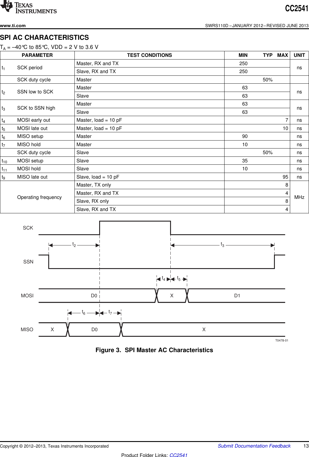
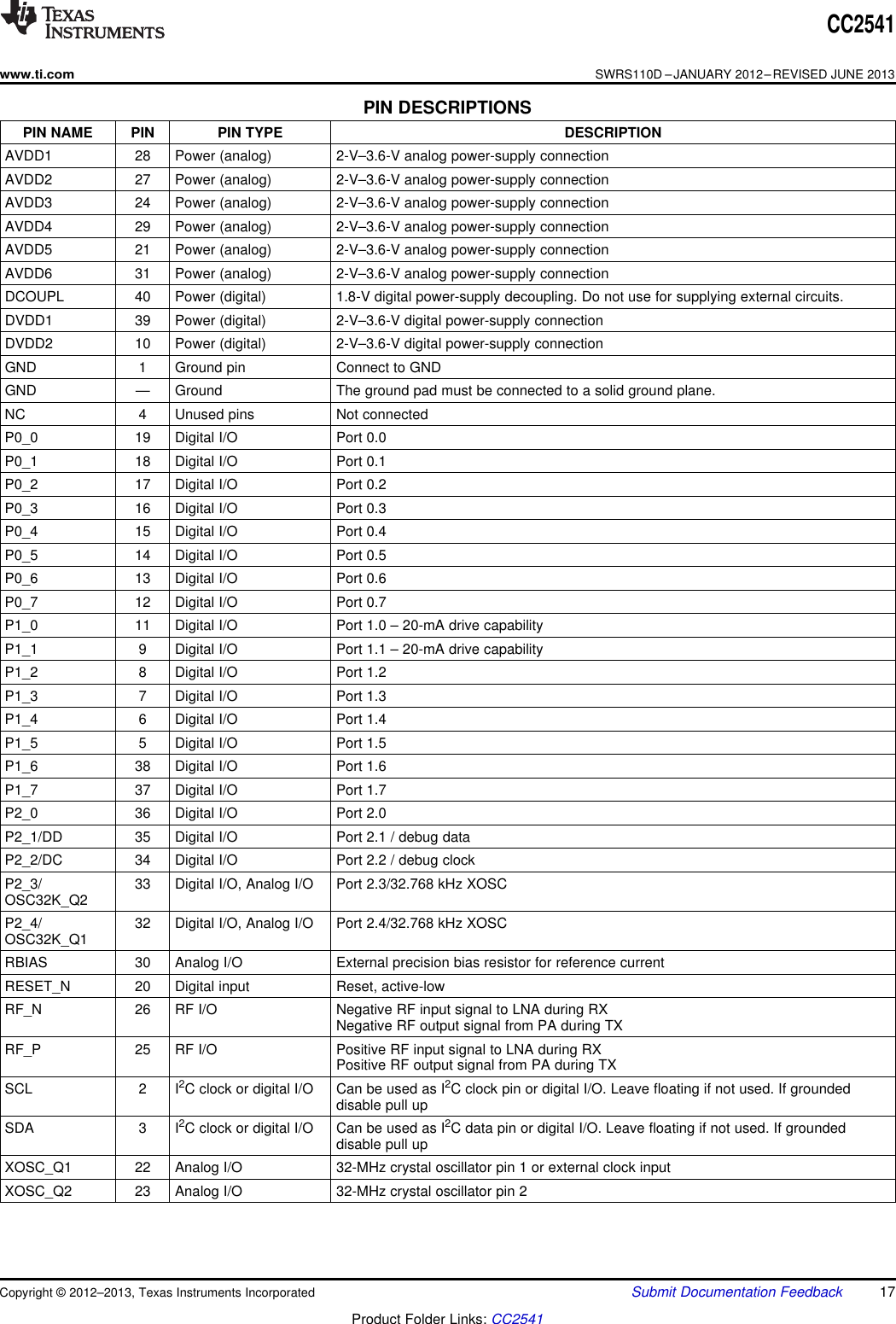
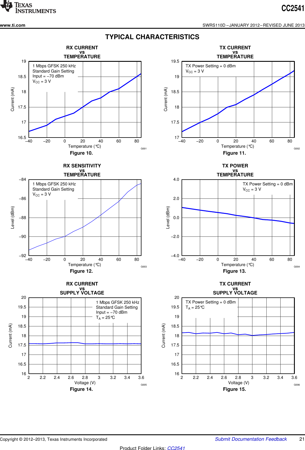
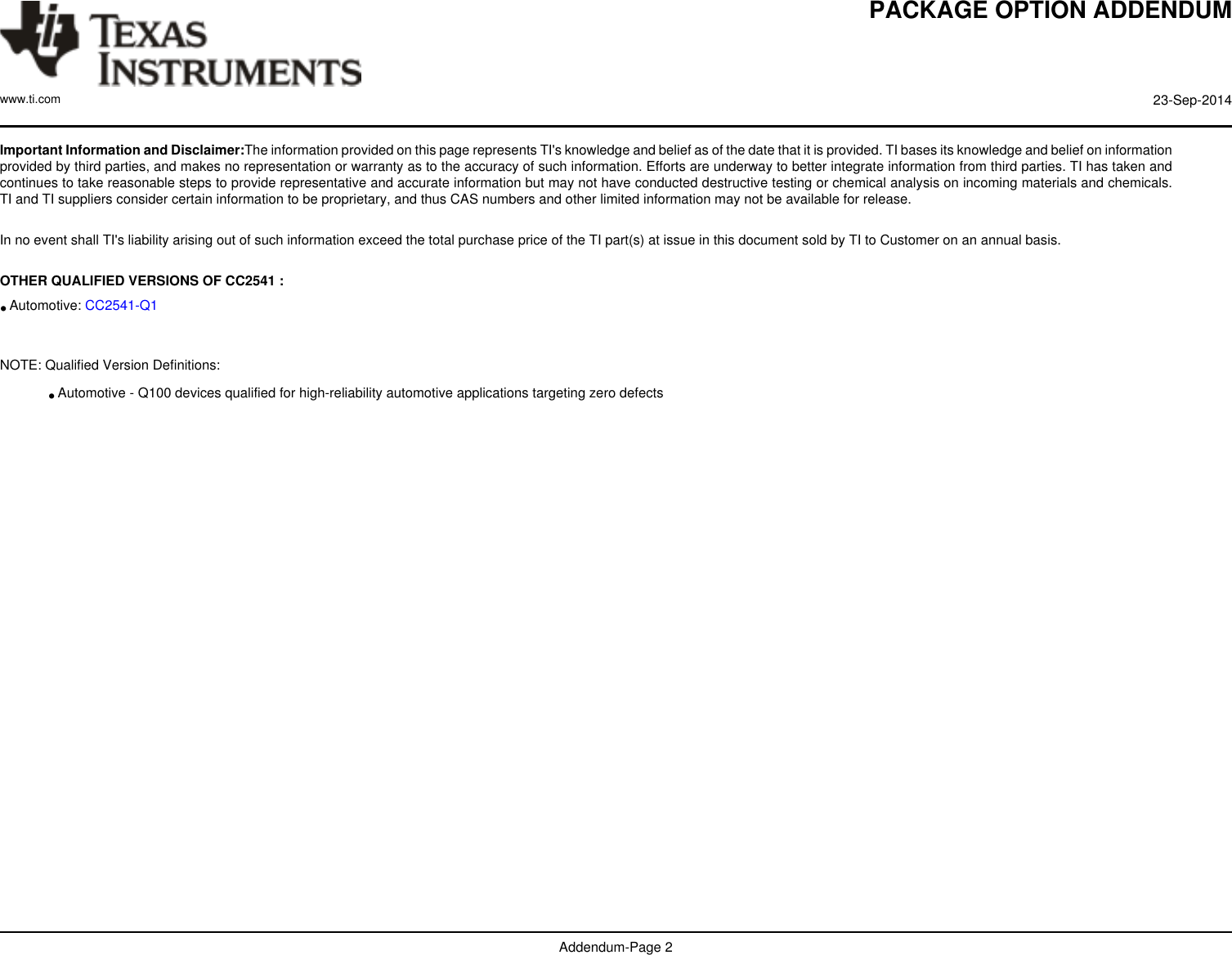
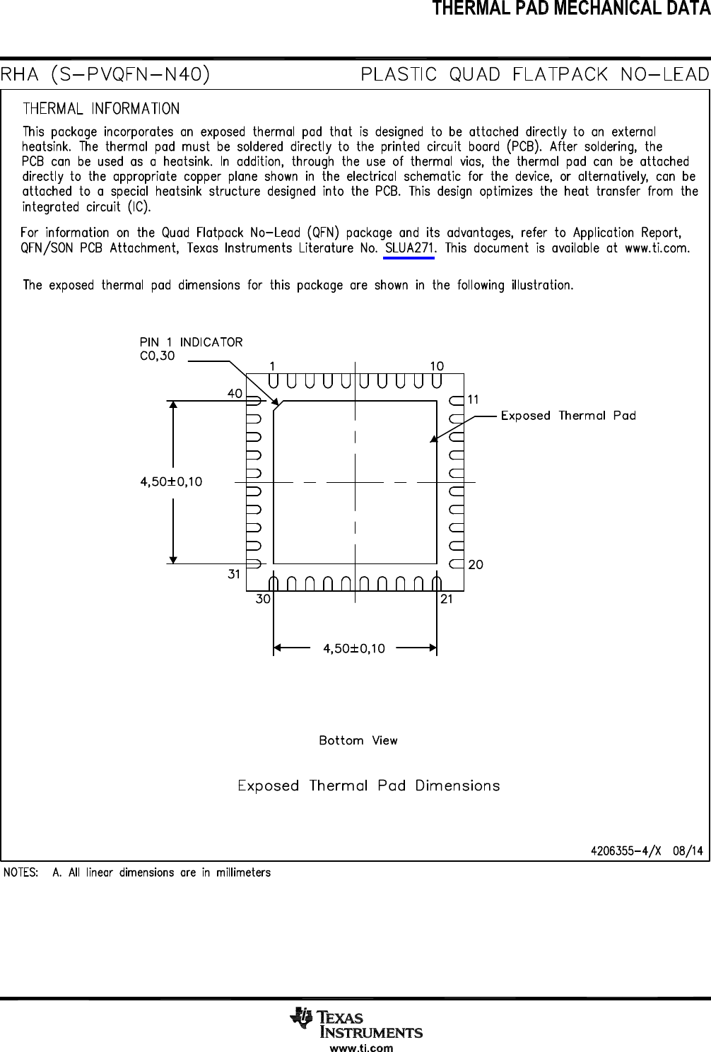
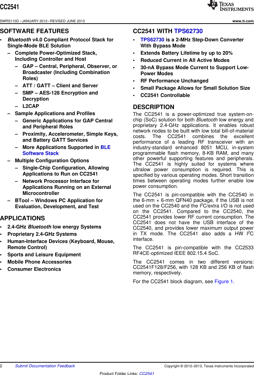
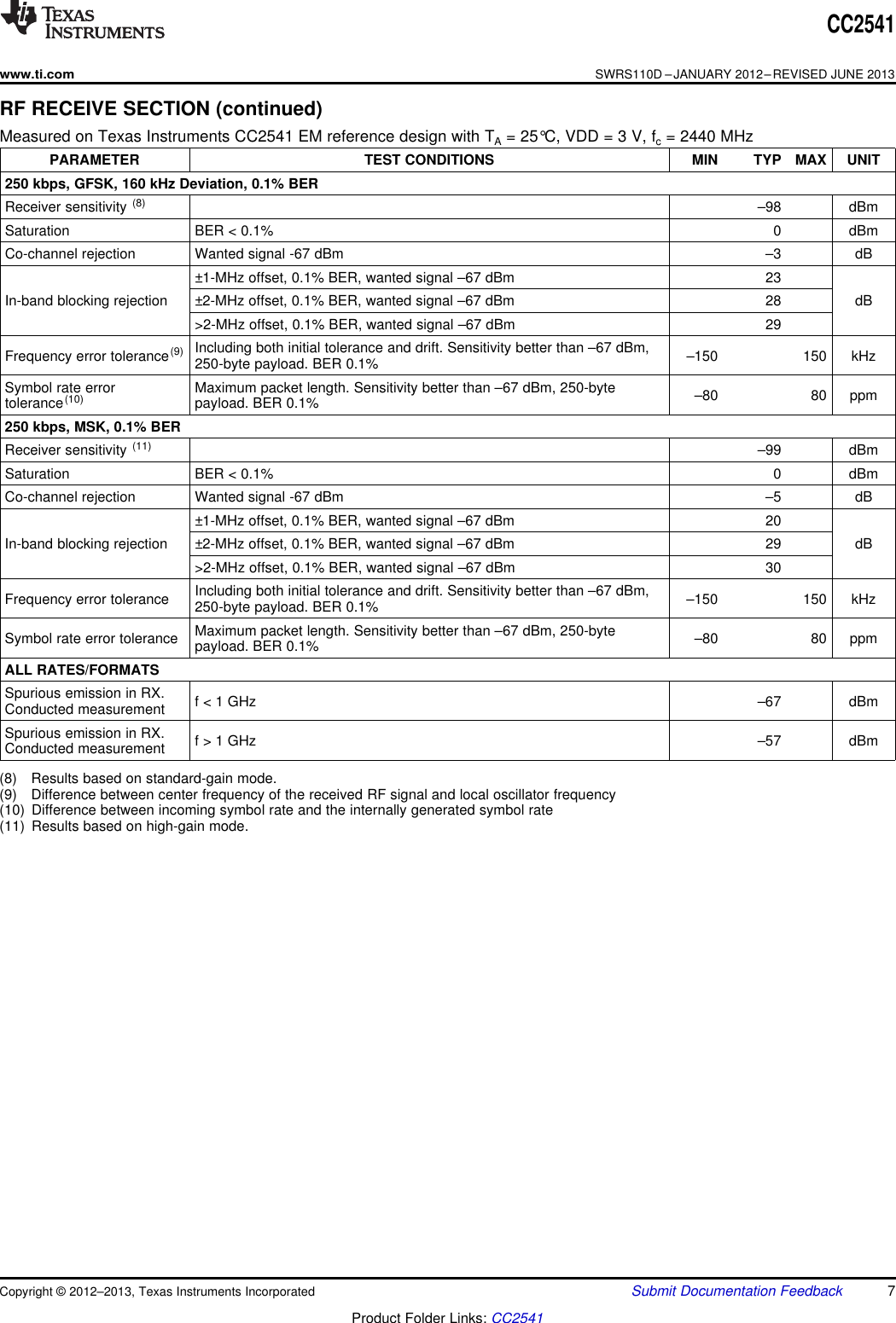
![GNDSCLSDANCP1_5DVDD2P1_1P1_2P1_3P1_42-V to 3.6-V Power SupplyR301XTAL1C221 C231XTAL2C321C331C40132-kHz Crystal(1)CC2541DIE ATTACH PADRBIASAVDD4AVDD1AVDD2RF_NAVDD5XOSC_Q1XOSC_Q2AVDD3RF_PP1_0P0_7P0_6P0_5P0_4RESET_NP0_0P0_1P0_2P0_3DCOUPLDVDD1P1_6P1_7P2_0AVDD6P2_4/XOSC32K_Q1P2_3/XOSC32K_Q2P2_2P2_1Antenna(50 )W12345678910111213141516171819202122232425262728293031323334353637383940Power Supply Decoupling Capacitors are Not ShownDigital I/O Not ConnectedCC2541SWRS110D –JANUARY 2012–REVISED JUNE 2013www.ti.comAPPLICATION INFORMATIONFew external components are required for the operation of the CC2541. A typical application circuit is shown inFigure 22.(1) 32-kHz crystal is mandatory when running the BLE protocol stack in low-power modes, except if the link layer is inthe standby state (Vol. 6 Part B Section 1.1 in [1]).NOTE: Different antenna alternatives will be provided as reference designs.Figure 22. CC2541 Application CircuitTable 3. Overview of External Components (Excluding Supply Decoupling Capacitors)Component Description ValueC401 Decoupling capacitor for the internal 1.8-V digital voltage regulator 1 µFR301 Precision resistor ±1%, used for internal biasing 56 kΩInput/Output MatchingWhen using an unbalanced antenna such as a monopole, a balun should be used to optimize performance. Thebalun can be implemented using low-cost discrete inductors and capacitors. See reference design, CC2541EM,for recommended balun.24 Submit Documentation Feedback Copyright © 2012–2013, Texas Instruments IncorporatedProduct Folder Links: CC2541](https://usermanual.wiki/iRobot/ALT240ROB.Chipset-Datasheet/User-Guide-2910061-Page-24.png)