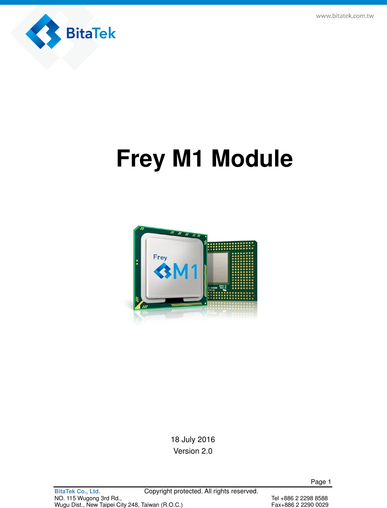
iWaylink IM0002 Frey User Manual IT7000N user Menu

Bitatek Co., Ltd. Frey IT7000N user Menu

Contents

Users Manual

  Page 1 BitaTek Co., Ltd.               Copyright protected. All rights reserved. NO. 115 Wugong 3rd Rd.,  Tel +886 2 2298 8588 Wugu Dist., New Taipei City 248, Taiwan (R.O.C.)  Fax+886 2 2290 0029    Frey M1 Module           18 July 2016 Version 2.0
  Page 2 BitaTek Co., Ltd.               Copyright protected. All rights reserved. NO. 115 Wugong 3rd Rd.,  Tel +886 2 2298 8588 Wugu Dist., New Taipei City 248, Taiwan (R.O.C.)  Fax+886 2 2290 0029 Contents  Charpt 1.  Revision History ..................................................................... 4 Charpt 2.  Introduction ............................................................................ 5 Charpt 3.  Product Concept .................................................................... 6 3.1.  Main Feature .......................................................................... 6 3.1.1.  Chipset on module ................................................................. 6 3.1.2.  Memory .................................................................................. 6 3.1.3.  Multimedia ............................................................................. 6 3.1.4.  Audio (PM8952 codec ) ......................................................... 7 3.1.5.  Expansion Slot Interface ........................................................ 7 3.1.6.  USB ....................................................................................... 7 3.1.7.  Keypad................................................................................... 7 3.1.8.  Dimension .............................................................................. 7 3.1.9.  Operation temperature ........................................................... 7 3.2.  Module Block Diagram ........................................................... 8 3.3.  Pin Definition .......................................................................... 8 3.4.  Pad assignments (Top view) ................................................ 27 3.5.  Electrical Specification ......................................................... 28 3.5.1.  Input power specification ..................................................... 28 3.5.2.  Output power specification ................................................... 29 3.5.3.  Current consumption ........................................................... 32 3.5.4.  Digital logic characteristics ................................................... 32 3.5.5.  Coin-cell charging ................................................................ 34 3.5.6.  Audio ................................................................................... 34 3.5.7.  Vibrator ................................................................................ 37 3.5.8.  Display ± bias ...................................................................... 37 3.5.9.  Flash drivers (including torch mode) .................................... 38 3.5.10.  Display backlight (WLEDs) .................................................. 39 3.5.11.  System clock (BB_CLK)....................................................... 40 3.5.12.  RF Transmit and Receiver Specifications ............................ 40 3.5.13.  Electrostatic Discharge ........................................................ 42 Charpt 4.  Module Mounting Issues ...................................................... 44 4.1.  Solder Paste ........................................................................ 44 4.2.  Stencil Printing ..................................................................... 44
  Page 3 BitaTek Co., Ltd.               Copyright protected. All rights reserved. NO. 115 Wugong 3rd Rd.,  Tel +886 2 2298 8588 Wugu Dist., New Taipei City 248, Taiwan (R.O.C.)  Fax+886 2 2290 0029 4.2.1.  General Stencil Considerations ........................................... 44 4.2.2.  Used Parameters and Recommendations ........................... 45 4.2.3.  Pick and Place ..................................................................... 45 4.2.4.  Reflow Profile ....................................................................... 45 4.3.  Soldering Conditions and Temperature ............................... 47 4.3.1.  Reflow Profile ....................................................................... 47 4.3.2.  Maximum Temperature and Duration .................................. 48 4.4.  Soldering Process Evaluation .............................................. 48 4.4.1.  Visual Inspection .................................................................. 48 4.4.2.  X-Ray Inspection and Void Content ..................................... 48 4.5.  Board Level Reliability Investigation .................................... 49 4.6.  Desoldering Process ............................................................ 50 4.6.1.  Preparation of LGA Module ................................................. 51 4.6.2.  Baking of Application Board ................................................. 51 4.6.3.  Removal of LGA Module ...................................................... 51 Charpt 5.  Packaging ............................................................................ 52 5.1.  Mechanical Dimensions of Frey M1 ..................................... 52 5.2.  Shipping Materials ............................................................... 54 5.2.1.  Moisture Barrier Bag ............................................................ 56 5.3.  Packing Label ...................................................................... 58 5.4.  Storage Conditions .............................................................. 62 5.5.  Moisture Sensitivity Level .................................................... 63 5.6.  Durability and Mechanical Handling ..................................... 63 5.6.1.  Storage Life ......................................................................... 63 5.6.2.  Processing Life .................................................................... 63 5.6.3.  Electrostatic Discharge ........................................................ 63 Charpt 6.  Regulatory and Type Approval Information.......................... 64 6.1.  Safety Precautions ............................................................... 66 6.2.  Safety .................................................................................. 68 Charpt 7.  Appendix .............................................................................. 70 7.1.  Abbreviations ....................................................................... 70 7.2.  Mounting Advice Sheet ........................................................ 70
  Page 4 BitaTek Co., Ltd.               Copyright protected. All rights reserved. NO. 115 Wugong 3rd Rd.,  Tel +886 2 2298 8588 Wugu Dist., New Taipei City 248, Taiwan (R.O.C.)  Fax+886 2 2290 0029 Charpt 1.    Revision History Changes to the original manual are listed below: Version Date Description 1.00 2016/06/21 Initial release 2.00 2016/7/18 Update FCC statement
  Page 5 BitaTek Co., Ltd.               Copyright protected. All rights reserved. NO. 115 Wugong 3rd Rd.,  Tel +886 2 2298 8588 Wugu Dist., New Taipei City 248, Taiwan (R.O.C.)  Fax+886 2 2290 0029 Charpt 2.  Introduction This document defines the specification for FREY M1. FREY M1 is a smart module for handheld device and builds in Bluetooth, WiFi and GPS function. It also can support SD card, LCM , Touch Screen , Audio , dual camera , Flash LED , Accelerometer / Magnetometer / Gyroscope / Proximity & Light Sensor functions through application design board.
  Page 6 BitaTek Co., Ltd.               Copyright protected. All rights reserved. NO. 115 Wugong 3rd Rd.,  Tel +886 2 2298 8588 Wugu Dist., New Taipei City 248, Taiwan (R.O.C.)  Fax+886 2 2290 0029 Charpt 3.  Product Concept 3.1.  Main Feature   3.1.1.  Chipset on module     Digital processor : APQ8052 (ARM Cortex-A53 octa cores)   Quad core at 1.516 GHz, 512 kB L2 cache     Quad core at 1.209 GHz, 512 kB L2 cache     Power management : PM8952 and PMI8952     WLAN/BT/FM : WCN3680B     WLAN IEEE 802.11a/b/g/n/ac dual bands   Bluetooth V2.1BER/EDR+3.0HS+4.1 LE     FM RDS & RBDS, RX only     GPS : WGR7640     GPS, Glonass , Galileo or Beidou  3.1.2.  Memory     eMCP , 2GB LPDDR3 RAM plus 16GB eMMC Flash ROM  3.1.3.  Multimedia     Display interface:     Support one 4-lane MIPI DSI port , FHD (1920 × 1200) 60 fps     Camera interface:     Support 4-lane + 4-lane or 4-lane + 2-lane + 1-lane MIPI CSI port   Two Flash LED interface     Graphics:    Qualcomm® Adreno™ 405     Touch screen:     Capacitive panels via external IC by I2C
  Page 7 BitaTek Co., Ltd.               Copyright protected. All rights reserved. NO. 115 Wugong 3rd Rd.,  Tel +886 2 2298 8588 Wugu Dist., New Taipei City 248, Taiwan (R.O.C.)  Fax+886 2 2290 0029 3.1.4.  Audio (PM8952 codec )     Support two Microphones interface with noise cancellation     Support one speaker interface   Support one receiver interface   Support one audio jack interface     Support one vibrator control interface    3.1.5.  Expansion Slot Interface     One micro SD Memory slot interface with SDHC     UIM interface x1    3.1.6.  USB   Support one USB OTG    3.1.7.  Keypad     Support 5x5 Key matrix    3.1.8.  Dimension     44 x 33.6 x 2.7 mm  3.1.9.  Operation temperature   Item Min. Typ. Max. Unit Normal temperature range Extreme temperature range +15 -30 +25  +55 +70 °C °C
  Page 8 BitaTek Co., Ltd.               Copyright protected. All rights reserved. NO. 115 Wugong 3rd Rd.,  Tel +886 2 2298 8588 Wugu Dist., New Taipei City 248, Taiwan (R.O.C.)  Fax+886 2 2290 0029 3.2.  Module Block Diagram  3.3.  Pin Definition AI : Analog input ;              AO : Analog output ; DI : Digital input ;                  DO : Digital output PI : Power input ;                  PO : Power output Pin Number Pin Name Wakeup Pad Type Functional description Power W18 USB_VBUS_IN  PI, PO Input power from selected source, or output during USB-OTG. W19 USB_VBUS_IN  PI, PO Input power from selected source, or output during USB-OTG. X18 USB_VBUS_IN  PI, PO Input power from selected source, or output during
  Page 9 BitaTek Co., Ltd.               Copyright protected. All rights reserved. NO. 115 Wugong 3rd Rd.,  Tel +886 2 2298 8588 Wugu Dist., New Taipei City 248, Taiwan (R.O.C.)  Fax+886 2 2290 0029 USB-OTG. X19 USB_VBUS_IN  PI, PO Input power from selected source, or output during USB-OTG. T18 VBATT  PI, PO Battery power supply T19 VBATT  PI, PO Battery power supply U18 VBATT  PI, PO Battery power supply U19 VBATT  PI, PO Battery power supply Z18 VPH_PWR  PI, PO Primary system power supply node Z19 VPH_PWR  PI, PO Primary system power supply node AA18 VPH_PWR  PI, PO Primary system power supply node AA19 VPH_PWR  PI, PO Primary system power supply node U16 VREG_L1  PO LDO output F16 VREG_L4  PO LDO output C15 VREG_L5  PO LDO output F12 VREG_L6  PO LDO output C19 VREG_L10  PO LDO output D17 VREG_L11  PO LDO output E13 VREG_L12  PO LDO output C18 VREG_L14  PO LDO output C16 VREG_L16  PO LDO output E16 VREG_L17  PO LDO output D19 VREG_L18  PO LDO output D18 VREG_L22  PO LDO output T17 VREG_L23  PO LDO output U17 PMI8952_VBIAS  PO Dedicated voltage source for battery-related resistor networks, not use for other purpose. X20 SYSON  PO LDO output that supplies SCHG FET drivers RTC Battery
  Page 10 BitaTek Co., Ltd.               Copyright protected. All rights reserved. NO. 115 Wugong 3rd Rd.,  Tel +886 2 2298 8588 Wugu Dist., New Taipei City 248, Taiwan (R.O.C.)  Fax+886 2 2290 0029 P20 VCOIN  PI, PO For RTC battery. Clock   F17 PM8952_BB_CLK2  DO Buffered baseband (low-power) XO clock 2 System W17 KYPD_PWR_N  DI Internal pull-up to dVdd; keep C load < 10 pF. Dual function: 1. Keypad power on; initiates power on when grounded 2. Can be configured as stage 2 or stage 3 reset if held LOW longer X15 RESIN_N  DI PMIC reset input ; initiates stage 2 or stage 3 reset if held LOW W20 PMI8952_CHG_EN  DI Charger enable   V20 CHG_VBAT_SNS  AI Sensed  battery  voltage  for charger circuits T20 BATT_ID  AI Battery ID input to ADC; also detects missing battery Y16 CS_MINUS  AI Current sense resistor — minus side (low side) V15 CS_PLUS  AI Current sense resistor — plus side (high side) V16 BATT_MINUS  AI Battery minus (-) terminal sense input   U15 BATT_PLUS  AI Battery  plus  (+)  terminal sense input X17 BATT_THERM  AI Battery temperature input to ADC (measures pack temperature) , default NTC is 47KΩ±1% in EVB battery .
  Page 11 BitaTek Co., Ltd.               Copyright protected. All rights reserved. NO. 115 Wugong 3rd Rd.,  Tel +886 2 2298 8588 Wugu Dist., New Taipei City 248, Taiwan (R.O.C.)  Fax+886 2 2290 0029 V17 PA_THERM  AI AMUX input – PA thermistor divider V19 PMI8952_USB_EN  DO Enable USB path from external power multiplexer Y18 PMI8952_USB_SNS  AI USB input voltage sense pin from external power multiplexer V18 PMI8952_DC_EN  DO Enable 2nd power path from external power multiplexer Y19 PMI8952_DC_SNS  AI 2nd power voltage sense to determine in or out of valid range Z16 NC  NC Keep it floating and doesn't connect to GND. Audio H18 MIC_BIAS1  AO Microphone bias #1 I18 MIC_BIAS2  AO Microphone bias #2 H19 MIC1_IN_M  AI Microphone input 1, minus H20 MIC1_IN_P  AI Microphone input 1, plus M19 MIC2_IN  AI Microphone input 2 L18 MIC3_IN  AI Microphone input 3 K18 GND_CFILT  GND Microphone  bias  filter ground J19 HPH_L  AO Headphone output, left channel J20 HPH_R  AO Headphone  output,  right channel K20 HPH_REF  AI Headphone ground reference N18 HS_DET  AI Headset detection L20 EARO_M  AO Earpiece output, minus (-) L19 EARO_P  AO Earpiece output, plus (+) N20 SPKR_DRV_M  AO Class-D speaker driver output, minus (-) N19 SPKR_DRV_P  AO Class-D speaker driver
  Page 12 BitaTek Co., Ltd.               Copyright protected. All rights reserved. NO. 115 Wugong 3rd Rd.,  Tel +886 2 2298 8588 Wugu Dist., New Taipei City 248, Taiwan (R.O.C.)  Fax+886 2 2290 0029 output, plus (+) Vibrator Y15 HAP_OUT_N  AO Vibrator driver output negative Y14 HAP_OUT_P  AO Vibrator driver output positive SD V1 SDC2_CLK  DO Secure digital controller 2 clock X2 SDC2_CMD    DI,DO Secure digital controller 2 command W1 SDC2_DATA_0    DI,DO Secure digital controller 2 data bit 0 V2 SDC2_DATA_1  DI,DO Secure digital controller 2 data bit 1 V3 SDC2_DATA_2  DI,DO Secure  digital  controller  2 data bit 2 W2 SDC2_DATA_3  DI,DO Secure  digital  controller  2 data bit 3 USB Z15 PMI8952_USB_ID  AI, AO Dual function: 1. OTG mode enable (programmable polarity; can also be controlled by OTG enable bit) 2. OTG ID monitor to detect the OTG ID resistor value. H13 USB_HS_DM  DI,DO USB HS data minus H14 USB_HS_DP  DI,DO USB HS data plus R19 PMI_USB_DM  DI USB data minus for power source detection only; modem IC handles data transactions R18 PMI_USB_DP  DI USB data plus for power source detection only; modem IC handles data
  Page 13 BitaTek Co., Ltd.               Copyright protected. All rights reserved. NO. 115 Wugong 3rd Rd.,  Tel +886 2 2298 8588 Wugu Dist., New Taipei City 248, Taiwan (R.O.C.)  Fax+886 2 2290 0029 transactions LED driver X9 VREG_WLED_ANODE  PO LCM WLED boost output Y13 WLED_SINK1  AO WLED low-side current sink input, string 1 Z14 WLED_SINK2  AO WLED low-side current sink input, string 2 Y12 WLED_SINK3  AO WLED low-side current sink input, string 3 Z12 WLED_SINK4  AO WLED low-side current sink input, string 4 W14 WLED_CABC  DI Content adaptive backlight control (CABC); PWM signal from display controller for dynamic dimming of LCD X16 FLASH_LED1  AO High-side current source for flash/torch LED1 anode Z17 FLASH_LED2  AO High-side current source for flash/torch LED2 anode Y17 CHARGE_LED_RED  AO Current sink for charging indication Display V14 VREG_DISP_N5V    PO Regulated output for the display’s negative bias V13 VREG_DISP_P5V  PO Regulated  output  for  the display’s positive bias U14 NC  NC Keep it floating and doesn't connect to GND. K2 MIPI_DSI_CLK_N  DO MIPI DSI clock negative K3 MIPI_DSI_CLK_P  DO MIPI DSI clock positive J2 MIPI_DSI_LN0_N  DO MIPI DSI data0 negative J3 MIPI_DSI_LN0_P  DO MIPI DSI data0 positive I2 MIPI_DSI_LN1_N  DO MIPI DSI data1 negative I1 MIPI_DSI_LN1_P  DO MIPI DSI data1 positive
  Page 14 BitaTek Co., Ltd.               Copyright protected. All rights reserved. NO. 115 Wugong 3rd Rd.,  Tel +886 2 2298 8588 Wugu Dist., New Taipei City 248, Taiwan (R.O.C.)  Fax+886 2 2290 0029 K1 MIPI_DSI_LN2_N  DO MIPI DSI data2 negative J1 MIPI_DSI_LN2_P  DO MIPI DSI data2 positive L2 MIPI_DSI_LN3_N  DO MIPI DSI data3 negative L3 MIPI_DSI_LN3_P  DO MIPI DSI data3 positive CAMERA P3 MIPI_CSI0_CLK_N  DI MIPI CSI clock negative P2 MIPI_CSI0_CLK_P  DI MIPI CSI0 clock positive Q2 MIPI_CSI0_LN0_N  DI MIPI CSI0 data0 negative Q3 MIPI_CSI0_LN0_P  DI MIPI CSI0 data0 positive R2 MIPI_CSI0_LN2_N  DI MIPI CSI0 data1 negative S2 MIPI_CSI0_LN2_P  DI MIPI CSI0 data1 positive S1 MIPI_CSI0_LN3_N  DI MIPI CSI0 data2 negative R1 MIPI_CSI0_LN3_P  DI MIPI CSI0 data2 positive Q1 MIPI_CSI0_LN4_N  DI MIPI CSI0 data3 negative P1 MIPI_CSI0_LN4_P  DI MIPI CSI0 data3 positive N3 MIPI_CSI1_CLK_N  DI MIPI CSI1 clock negative N2 MIPI_CSI1_CLK_P  DI MIPI CSI1 clock positive O3 MIPI_CSI1_LN0_N  DI MIPI CSI1 data0 negative O2 MIPI_CSI1_LN0_P  DI MIPI CSI1 data0 positive N1 MIPI_CSI1_LN2_N  DI MIPI CSI1 data1 negative O1 MIPI_CSI1_LN2_P  DI MIPI CSI1 data1 positive M3 MIPI_CSI1_LN3_N  DI MIPI CSI1 data2 negative M2 MIPI_CSI1_LN3_P  DI MIPI CSI1 data2 positive L1 MIPI_CSI1_LN4_N  DI MIPI CSI1 data3 negative M1 MIPI_CSI1_LN4_P  DI MIPI CSI1 data3 positive Antenna A2 WLAN_BT_ANT  ANT WLAN/BT antenna A19 GPS_ANT  ANT GPS antenna A13 FM_ANT  ANT FM RX antenna MPP(Multi-Purpose Pin) X14 PMI8952_MPP_1  MPP 1. Configurable as digital I/Os   2. Analog multiplexer inputs 3. Even MPPs configurable as current sinks; odd MPPs
  Page 15 BitaTek Co., Ltd.               Copyright protected. All rights reserved. NO. 115 Wugong 3rd Rd.,  Tel +886 2 2298 8588 Wugu Dist., New Taipei City 248, Taiwan (R.O.C.)  Fax+886 2 2290 0029 configurable as analog outputs X13 PMI8952_MPP_2  MPP 1. Configurable as digital I/Os   2. Analog multiplexer inputs 3. Even MPPs configurable as current sinks; odd MPPs configurable as analog outputs W13 PMI8952_MPP_3  MPP 1. Configurable as digital I/Os   2. Analog multiplexer inputs 3. Even MPPs configurable as current sinks; odd MPPs configurable as analog outputs G16 PM8952_MPP_02  MPP 1. Configurable as digital I/Os 2. Level-translating bidirectional I/Os 3. Analog multiplexer inputs 4. Even MPPs can be current sinks and odd MPPs can be VREF buffer outputs F15 PM8952_MPP_03  MPP 1. Configurable as digital I/Os 2. Level-translating bidirectional I/Os 3. Analog multiplexer inputs 4. Even MPPs can be current sinks and odd MPPs can be VREF buffer outputs G15 PM8952_MPP_04  MPP 1. Configurable as digital I/Os
  Page 16 BitaTek Co., Ltd.               Copyright protected. All rights reserved. NO. 115 Wugong 3rd Rd.,  Tel +886 2 2298 8588 Wugu Dist., New Taipei City 248, Taiwan (R.O.C.)  Fax+886 2 2290 0029 2. Level-translating bidirectional I/Os 3. Analog multiplexer inputs 4. Even MPPs can be current sinks and odd MPPs can be VREF buffer outputs GPIO E2 GPIO_0  GPIO 1. Configurable I/O 2. BLSP1_SPI_MOSI 3. BLSP1_UART_TX F2 GPIO_1  GPIO 1. Configurable I/O 2. BLSP3_SPI_CS_N 3. BLSP3_I2C_SDA 4. GP_CLK_2B E3 GPIO_2 V GPIO 1. Configurable I/O 2. BLSP8_SPI_MISO F3 GPIO_3  GPIO 1. Configurable I/O 2. BLSP1_SPI_CLK 3. BLSP1_UART_RFR_N 4. BLSP1_I2C_SCL U4 GPIO_4  GPIO 1. Configurable I/O 2. BLSP2_SPI_MOSI 3. BLSP2_UART_TX T4 GPIO_5 V GPIO 1. Configurable I/O 2. BLSP2_SPI_MISO 3. BLSP2_UART_RX 4. LDO_EN X3 GPIO_6  GPIO 1. Configurable I/O 2. BLSP2_SPI_CS_N 3. BLSP2_UART_CTS_N 4. BLSP2_I2C_SDA 5. GP_CLK_1B W3 GPIO_7  GPIO 1. Configurable I/O 2. BLSP2_SPI_CLK 3. BLSP2_UART_RFR_N
  Page 17 BitaTek Co., Ltd.               Copyright protected. All rights reserved. NO. 115 Wugong 3rd Rd.,  Tel +886 2 2298 8588 Wugu Dist., New Taipei City 248, Taiwan (R.O.C.)  Fax+886 2 2290 0029 4. BLSP2_I2C_SCL 5. GP_PDM_2A I3 GPIO_8  GPIO 1. Configurable I/O H2 GPIO_9  GPIO 1. Configurable I/O G3 GPIO_10 V GPIO 1. Configurable I/O 2. BLSP1_SPI_MISO 3. BLSP1_UART_RX G2 GPIO_11  GPIO 1. Configurable I/O 2. BLSP3_SPI_CLK 3. BLSP3_I2C_SCL 4. GP_CLK_3B D4 GPIO_12 V GPIO 1. Configurable I/O 2. BLSP4_SPI_MOSI 3. MI2S_2_D0 D1 GPIO_13 V GPIO 1. Configurable I/O 2. BLSP4_SPI_MISO 3. MI2S_2_D1 F1 GPIO_14  GPIO 1. Configurable I/O 2. BLSP4_SPI_CS_N 3. BLSP4_I2C_SDA E1 GPIO_15  GPIO 1. Configurable I/O 2. BLSP4_SPI_CLK 3. BLSP4_I2C_SCL E4 GPIO_16  GPIO 1. Configurable I/O 2. BLSP5_SPI_MOSI 3. BLSP5_UART_TX G4 GPIO_17 V GPIO 1. Configurable I/O 2. BLSP5_SPI_MISO 3. BLSP5_UART_RX B4 GPIO_18  GPIO 1. Configurable I/O 2. BLSP5_SPI_CS_N 3. BLSP5_UART_CTS_N 4. BLSP5_I2C_SDA C4 GPIO_19  GPIO 1. Configurable I/O 2. BLSP5_SPI_CLK 3. BLSP5_UART_RFR_N
  Page 18 BitaTek Co., Ltd.               Copyright protected. All rights reserved. NO. 115 Wugong 3rd Rd.,  Tel +886 2 2298 8588 Wugu Dist., New Taipei City 248, Taiwan (R.O.C.)  Fax+886 2 2290 0029 4. BLSP5_I2C_SCL V9 GPIO_20  GPIO 1. Configurable I/O 2. BLSP6_SPI_MOSI 3. BLSP6_UART_TX 4. GP_PDM_1B W9 GPIO_21 V GPIO 1. Configurable I/O 2. BLSP6_SPI_MISO 3. BLSP6_UART_RX T15 GPIO_22  GPIO 1. Configurable I/O 2. BLSP6_SPI_CS_N 3. BLSP6_UART_CTS_N 4. BLSP6_I2C_SDA T16 GPIO_23  GPIO 1. Configurable I/O C1 GPIO_24  GPIO 1. Configurable I/O 2. SDE_VSYNC_P G1 GPIO_25 V GPIO 1. Configurable I/O 2. SDE_VSYNC_S 3. PRI_MI2S_MCLK_A 4. SEC_MI2S_MCLK_A T12 GPIO_26  GPIO 1. Configurable I/O Y9 GPIO_27  GPIO 1. Configurable I/O 2. CAM_MCLK1 T13 GPIO_28   1. Configurable I/O 2. CAM_MCLK2 Y11 GPIO_29  GPIO 1. Configurable I/O 2. BLSP6_SPI_CS2_N 3. GP_CLK1 Z11 GPIO_30  GPIO 1. Configurable I/O 2. CCI_I2C0_SCL W10 GPIO_31 V GPIO 1. Configurable I/O 2. CCI_I2C1_SDA Y8 GPIO_32  GPIO 1. Configurable I/O 2. CCI_I2C1_SCL T8 GPIO_33  GPIO 1. Configurable I/O 2. CCI_TIMER0 X10 GPIO_35 V GPIO 1. Configurable I/O
  Page 19 BitaTek Co., Ltd.               Copyright protected. All rights reserved. NO. 115 Wugong 3rd Rd.,  Tel +886 2 2298 8588 Wugu Dist., New Taipei City 248, Taiwan (R.O.C.)  Fax+886 2 2290 0029 W11 GPIO_36 V GPIO 1. Configurable I/O W8 GPIO_37 V GPIO 1. Configurable I/O V8 GPIO_38 V GPIO 1. Configurable I/O Z8 GPIO_39  GPIO 1. Configurable I/O 2. CCI_ASYNC0 3. GP_MN Z13 GPIO_40  GPIO 1. Configurable I/O X11 GPIO_41  GPIO 1. Configurable I/O 2. SD_WRITE_PROTECT Z10 GPIO_42 V GPIO 1. Configurable I/O 2. GP_CLK_1A Y10 GPIO_43 V GPIO 1. Configurable I/O 2. GP_CLK_2A V12 GPIO_44 V GPIO 1. Configurable I/O 2. GP_CLK_3A T9 GPIO_45 V GPIO 1. Configurable I/O 2. GP_PDM_1A V10 GPIO_46 V GPIO 1. Configurable I/O 2. GP_CLK0 X12 GPIO_47  GPIO 1. Configurable I/O 2. CCI_I2C0_SDA U9 GPIO_48 V GPIO 1. Configurable I/O 2. BLSP6_SPI_CS2_N 3. GP_PDM_0B W12 GPIO_50  GPIO 1. Configurable I/O F14 GPIO_51  GPIO 1. Configurable I/O F13 GPIO_52  GPIO 1. Configurable I/O H12 GPIO_53  GPIO 1. Configurable I/O 2. UIM1_RESET B11 GPIO_54 V GPIO 1. Configurable I/O 2. UIM1_PRESENT G9 GPIO_57  GPIO 1. Configurable I/O 2. UIM2_RESET F11 GPIO_58 V GPIO 1. Configurable I/O 2. UIM2_PRESENT E14 GPIO_59  GPIO 1. Configurable I/O
  Page 20 BitaTek Co., Ltd.               Copyright protected. All rights reserved. NO. 115 Wugong 3rd Rd.,  Tel +886 2 2298 8588 Wugu Dist., New Taipei City 248, Taiwan (R.O.C.)  Fax+886 2 2290 0029 E12 GPIO_60  GPIO 1. Configurable I/O G12 GPIO_61  GPIO 1. Configurable I/O G11 GPIO_62 V GPIO 1. Configurable I/O T11 GPIO_63  GPIO 1. Configurable I/O 2. CAM_MCLK0 U13 GPIO_64  GPIO 1. Configurable I/O H6 GPIO_65 V GPIO 1. Configurable I/O T14 GPIO_67 V GPIO 1. Configurable I/O H3 GPIO_68  GPIO 1. Configurable I/O H4 GPIO_85 V GPIO 1. Configurable I/O D5 GPIO_86  GPIO 1. Configurable I/O E5 GPIO_87  GPIO 1. Configurable I/O C5 GPIO_88  GPIO 1. Configurable I/O 2. BLSP8_I2C_SDA 3. BLSP8_SPI_CS_N F6 GPIO_89  GPIO 1. Configurable I/O 2. DMIC0_CLK H8 GPIO_90 V GPIO 1. Configurable I/O 2. DMIC0_DATA A4 GPIO_91  GPIO 1. Configurable I/O 2. MI2S_1_SCK B5 GPIO_92  GPIO 1. Configurable I/O 2. BLSP7_SPI_MOSI 3. MI2S_1_WS A5 GPIO_93 V GPIO 1. Configurable I/O 2. BLSP7_SPI_MISO 3. MI2S_1_D0 D2 GPIO_94  GPIO 1. Configurable I/O 2. WSA_IO_DATA 3. BLSP7_SPI_CS_N 4. BLSP7_I2C_SDA D3 GPIO_95  GPIO 1. Configurable I/O 2. WSA_IO_CLK 3. BLSP7_SPI_CLK 4. BLSP7_I2C_SCL C2 GPIO_96  GPIO 1. Configurable I/O
  Page 21 BitaTek Co., Ltd.               Copyright protected. All rights reserved. NO. 115 Wugong 3rd Rd.,  Tel +886 2 2298 8588 Wugu Dist., New Taipei City 248, Taiwan (R.O.C.)  Fax+886 2 2290 0029 2. BLSP8_SPI_MOSI C6 GPIO_97  GPIO 1. Configurable I/O 2. BLSP1_SPI_CS_N 3. BLSP1_UART_CTS_N 4. BLSP1_I2C_SDA D6 GPIO_98  GPIO 1. Configurable I/O 2. MI2S_1_D1 C3 GPIO_99  GPIO 1. Configurable I/O 2. BLSP8_I2C_SCL 3. BLSP8_SPI_CLK D12 GPIO_100  GPIO 1. Configurable I/O 2. GRFC_0 E11 GPIO_101  GPIO 1. Configurable I/O 2. GRFC_1 C10 GPIO_102  GPIO 1. Configurable I/O 2. GRFC_2 D11 GPIO_103  GPIO 1. Configurable I/O 2. GRFC_3 D10 GPIO_104  GPIO 1. Configurable I/O 2. GRFC_4 H10 GPIO_105  GPIO 1. Configurable I/O 2. GRFC_5 B10 GPIO_106  GPIO 1. Configurable I/O H11 GPIO_110  GPIO 1.Configurable I/O 2. GRFC_10 E10 GPIO_115  GPIO 1.Configurable I/O 2. GRFC_15 3. GSM_TX_PHASE_TXDAC1 F10 GPIO_116  GPIO 1. Configurable I/O 2. GRFC_28 G10 GPIO_117  GPIO 1.Configurable I/O 2. SM_TX_PHASE_TXDAC0 3. GRFC_27
  Page 22 BitaTek Co., Ltd.               Copyright protected. All rights reserved. NO. 115 Wugong 3rd Rd.,  Tel +886 2 2298 8588 Wugu Dist., New Taipei City 248, Taiwan (R.O.C.)  Fax+886 2 2290 0029 F8 GPIO_118  GPIO 1.Configurable I/O 2. RFFE1_CLK E8 GPIO_119  GPIO 1.Configurable I/O 2. RFFE1_DATA G8 GPIO_120  GPIO 1. Configurable I/O 2. RFFE2_CLK G7 GPIO_121  GPIO 1. Configurable I/O 2. RFFE2_DATA G6 GPIO_122  GPIO 1. Configurable I/O 2. RFFE4_CLK G5 GPIO_123  GPIO 1. Configurable I/O 2. RFFE4_DATA H5 GPIO_124  GPIO 1. Configurable I/O 2. RFFE5_CLK F5 GPIO_125  GPIO 1. Configurable I/O 2. RFFE5_DATA H7 GPIO_126  GPIO 1. Configurable I/O 2. RFFE3_CLK F4 GPIO_127  GPIO 1. Configurable I/O 2. RFFE3_DATA W4 GPIO_128  GPIO 1. Configurable I/O V4 GPIO_129  GPIO 1. Configurable I/O T3 GPIO_130  GPIO 1. Configurable I/O X8 GPIO_131  GPIO 1. Configurable I/O U8 GPIO_132  GPIO 1. Configurable I/O Z9 GPIO_133  GPIO 1. Configurable I/O W15 PMI8952_GPIO_1  GPIO 1. Configurable I/O W16 PMI8952_GPIO_2  GPIO 1. Configurable I/O D16 PM8952_GPIO_01  GPIO 1. Configurable I/O D15 PM8952_GPIO_02  GPIO 1. Configurable I/O H16 PM8952_GPIO_04  GPIO 1. Configurable I/O C17 PM8952_GPIO_05  GPIO 1. Configurable I/O E15 PM8952_GPIO_06  GPIO 1. Configurable I/O P18 PM8952_GPIO_07  GPIO 1. Configurable I/O P19 PM8952_GPIO_08  GPIO 1. Configurable I/O GND
  Page 23 BitaTek Co., Ltd.               Copyright protected. All rights reserved. NO. 115 Wugong 3rd Rd.,  Tel +886 2 2298 8588 Wugu Dist., New Taipei City 248, Taiwan (R.O.C.)  Fax+886 2 2290 0029 A1 GND  GND  A3 GND  GND  A6 GND  GND  A7 GND  GND  A8 GND  GND  A9 GND  GND  A10 GND  GND  A11 GND  GND  A12 GND  GND  A14 GND  GND  A15 GND  GND  A16 GND  GND  A17 GND  GND  A18 GND  GND  A20 GND  GND  B1 GND  GND  B2 GND  GND  B3 GND  GND  B6 GND  GND  B7 GND  GND  B8 GND  GND  B9 GND  GND  B12 GND  GND  B13 GND  GND  B14 GND  GND  B15 GND  GND  B16 GND  GND  B17 GND  GND  B18 GND  GND  B19 GND  GND  B20 GND  GND  C7 GND  GND  C8 GND  GND  C9 GND  GND  C11 GND  GND
  Page 24 BitaTek Co., Ltd.               Copyright protected. All rights reserved. NO. 115 Wugong 3rd Rd.,  Tel +886 2 2298 8588 Wugu Dist., New Taipei City 248, Taiwan (R.O.C.)  Fax+886 2 2290 0029 C12 GND  GND  C13 GND  GND  C14 GND  GND  C20 GND  GND  D7 GND  GND  D8 GND  GND  D9 GND  GND  D13 GND  GND  D14 GND  GND  D20 GND  GND  E6 GND  GND  E7 GND  GND  E9 GND  GND  E17 GND  GND  E18 GND  GND  E19 GND  GND  E20 GND  GND  F7 GND  GND  F9 GND  GND  F18 GND  GND  F19 GND  GND  F20 GND  GND  G13 GND  GND  G14 GND  GND  G17 GND  GND  G18 GND  GND  G19 GND  GND  G20 GND  GND  H1 GND  GND  H9 GND  GND  H15 GND  GND  H17 GND  GND  I19 GND  GND  I20 GND  GND  J18 GND  GND
  Page 25 BitaTek Co., Ltd.               Copyright protected. All rights reserved. NO. 115 Wugong 3rd Rd.,  Tel +886 2 2298 8588 Wugu Dist., New Taipei City 248, Taiwan (R.O.C.)  Fax+886 2 2290 0029 K19 GND  GND  M18 GND  GND  M20 GND  GND  O18 GND  GND  O19 GND  GND  O20 GND  GND  Q18 GND  GND  Q19 GND  GND  Q20 GND  GND  R3 GND  GND  R20 GND  GND  S3 GND  GND  S18 GND  GND  S19 GND  GND  S20 GND  GND  T1 GND  GND  T2 GND  GND  T5 GND  GND  T6 GND  GND  T7 GND  GND  T10 GND  GND  U1 GND  GND  U2 GND  GND  U3 GND  GND  U5 GND  GND  U6 GND  GND  U7 GND  GND  U10 GND  GND  U11 GND  GND  U12 GND  GND  U20 GND  GND  V5 GND  GND  V6 GND  GND  V7 GND  GND  V11 GND  GND
  Page 26 BitaTek Co., Ltd.               Copyright protected. All rights reserved. NO. 115 Wugong 3rd Rd.,  Tel +886 2 2298 8588 Wugu Dist., New Taipei City 248, Taiwan (R.O.C.)  Fax+886 2 2290 0029 W5 GND  GND  W6 GND  GND  W7 GND  GND  X1 GND  GND  X4 GND  GND  X5 GND  GND  X6 GND  GND  X7 GND  GND  Y1 GND  GND  Y2 GND  GND  Y3 GND  GND  Y4 GND  GND  Y5 GND  GND  Y6 GND  GND  Y7 GND  GND  Y20 GND  GND  Z1 GND  GND  Z2 GND  GND  Z3 GND  GND  Z4 GND  GND  Z5 GND  GND  Z6 GND  GND  Z7 GND  GND  Z20 GND  GND  AA1 GND  GND  AA2 GND  GND  AA3 GND  GND  AA4 GND  GND  AA5 GND  GND  AA6 GND  GND  AA7 GND  GND  AA8 GND  GND  AA9 GND  GND  AA10 GND  GND  AA11 GND  GND
  Page 27 BitaTek Co., Ltd.               Copyright protected. All rights reserved. NO. 115 Wugong 3rd Rd.,  Tel +886 2 2298 8588 Wugu Dist., New Taipei City 248, Taiwan (R.O.C.)  Fax+886 2 2290 0029 AA12 GND  GND  AA13 GND  GND  AA14 GND  GND  AA15 GND  GND  AA16 GND  GND  AA17 GND  GND  AA20 GND  GND    3.4.  Pad assignments (Top view)
  Page 28 BitaTek Co., Ltd.               Copyright protected. All rights reserved. NO. 115 Wugong 3rd Rd.,  Tel +886 2 2298 8588 Wugu Dist., New Taipei City 248, Taiwan (R.O.C.)  Fax+886 2 2290 0029 3.5.  Electrical Specification 3.5.1.  Input power specification Absolute maximum rating: Operating FREY M1 under conditions beyond its absolute maximum ratings may damage the device. Absolute maximum ratings are limiting values to be considered individually when all other parameters are within their specified operating ranges. Functional operation and specification compliance under any absolute maximum condition, or after exposure to any of these conditions, is not guaranteed or implied. Exposure may affect device reliability. Parameter Min. Max. Units USB_VBUS_IN 0 25 V VPH_PWR 0 6 V CHG_OUT (VBAT) Steady state 0 5 V CHG_OUT (VBAT) Transient (< 10 ms) 0 6 V  Operation condition: Operating conditions include parameters that are under the control of the user : power supply voltage and ambient temperature. The FREY M1 meets all performance specifications listed in this document when used and/or stored within the operating conditions, unless otherwise noted in those sections (provided the absolute maximum ratings have never been exceeded). Parameter Min. Max. Units USB_VBUS_IN 4.0 10 V VPH_PWR 3.5 4.5 V CHG_OUT (VBAT) 3.5 4.5 V Note : There is battery detection algorithm in FREY M1 , user need to implement battery ID and thermal pin on the system , otherwise system can't be powered on successfully .
  Page 29 BitaTek Co., Ltd.               Copyright protected. All rights reserved. NO. 115 Wugong 3rd Rd.,  Tel +886 2 2298 8588 Wugu Dist., New Taipei City 248, Taiwan (R.O.C.)  Fax+886 2 2290 0029 Battery charger: The FREY M1 features a fully programmable switch-mode battery charger, input power and output power controller for terminal devices. The device is designed to be used in conjunction with systems using single-cell Li-ion and Li-polymer battery packs. Parameter Conditions Min Typ Max Units Peak switching current USB_IN = 9.0 V - 4 - A Maximum DC output current USB_IN = 9.0 V - 3 - A Switching frequency  0.95 1.0 1.05 MHz OTG output voltage  4.85 5.00 5.15 V Charger-specific digital I/O characteristics High-level input voltage (VIH) All charger digital interface pads except CHG_EN 1.5 - - V Low-level input voltage (VIL) - - 0.5 V CHG_EN high-level input voltage (VIH)  1.3 - - V CHG_EN low-level input voltage (VIL)  - - 0.3 V   3.5.2.  Output power specification Output power Circuit type Default voltage (V) Specified voltage range (V)6 Rated current (mA) Expected use VREG_L1 NMOS LDO 1.000 1.000 200 RFICs VREG_L4 PMOS LDO 1.800 1.800 450 RFICs and GPS eLNA VREG_L5 PMOS LDO 1.800 1.800 300 Most digital I/Os, LPDDR and eMMC
  Page 30 BitaTek Co., Ltd.               Copyright protected. All rights reserved. NO. 115 Wugong 3rd Rd.,  Tel +886 2 2298 8588 Wugu Dist., New Taipei City 248, Taiwan (R.O.C.)  Fax+886 2 2290 0029 VREG_L6 PMOS LDO 1.800 1.800 300 APQ DSI PLL and OTP, Camera, Touch screen, Display, and sensors VREG_L10 PMOS LDO 2.850 2.850 150 Sensors VREG_L11 PMOS LDO 2.950 2.950 800 Micro SD VREG_L12 PMOS LDO 2.950 1.800/2.950 150 APQ pad group 2 and SDC2 VREG_L14 PMOS LDO 1.800 1.800/3.300 50 APQ pad group 5, dual-voltage UIM1, and NFC VREG_L16 PMOS LDO 1.800 1.800 5 PMIC HKADC VREG_L17 PMOS LDO 2.850 2.850 600 Camera, Display, and Touch screen VREG_L18 PMOS LDO 2.700 2.700 150 QTI RF front-end VREG_L22 PMOS LDO 2.800 2.800 300 Camera – analog VREG_L23 NMOS LDO 1.200 1.200 300 Camera – digital
  Page 31 BitaTek Co., Ltd.               Copyright protected. All rights reserved. NO. 115 Wugong 3rd Rd.,  Tel +886 2 2298 8588 Wugu Dist., New Taipei City 248, Taiwan (R.O.C.)  Fax+886 2 2290 0029 LDO performance specifications Parameter Comments Min Typ Max Units Output voltage   All NMOS   All PMOS    12.5 mV steps   12.5 V steps  0.375 1.75  - -  1.5375 3.3375  V V Overall DC voltage output error   Normal mode  At default voltage  At non-default voltages  Low-power mode  At default voltage  At non-default voltages Over-voltage, temperature, and process variations plus load and line regulation   -2 -3   -4 -5   - -   - -   2 3   4 5   % %   % % Temperature coefficient  -100 - 100 ppm/°C NMOS power-supply ripple rejection   Normal mode  50 Hz–1 kHz  1–10 kHz  10–100 kHz  Low-power mode  50 Hz–1 kHz  1–100 kHz PSRR    60 - -  - -    70 60 50  50 40    - - -  - -    dB dB dB  dB dB PMOS power-supply ripple rejection   50 Hz–1 kHz   1–10 kHz  10–100 kHz        43 35 13   - - -   - - -   dB dB dB
  Page 32 BitaTek Co., Ltd.               Copyright protected. All rights reserved. NO. 115 Wugong 3rd Rd.,  Tel +886 2 2298 8588 Wugu Dist., New Taipei City 248, Taiwan (R.O.C.)  Fax+886 2 2290 0029 3.5.3.  Current consumption   Item Test condition Max. Units Off mode current Module is turned off   250 uA Flight mode current   Module is turned on and in sleep mode and all RF is turned off   4.5 mA WiFi TX current 2.4G, 11b, 11 Mbps, 15 dBm 250 mA WiFi RX current 2.4G 130 mA WiFi TX current 5G, 11a, 54 Mbps, 15 dBm 250 mA WiFi RX current 5G 130 mA BT TX current class 2 , 2dBm 150 mA BT RX current  130 mA Note 1. The measurement is at VBAT of module and VBAT=3.8V .   Note 2. WiFi & BT current is measured with IQexl 160.    3.5.4.  Digital logic characteristics Digital I/Os specification Pad voltage Usage Table 1.8 V Most digital I/Os Table 3.5.4.1 Dual-V (1.8 V/2.95 V) SDC2, UIM Table 3.5.4.2 Dual-V (1.8 V/3.05 V) USB Table 3.5.4.3  Table 3.5.4.1 Digital I/O (VDD_P3= VREG_L5) Parameter Min. Max. Unit VIH High-level input voltage 0.65 × VDD_P3 - V VIL Low-level input voltage - 0.35 × VDD_P3 V VOH High-level output voltage VDD_P3 - 0.45 - V VOL Low-level output voltage - 0.45 V
  Page 33 BitaTek Co., Ltd.               Copyright protected. All rights reserved. NO. 115 Wugong 3rd Rd.,  Tel +886 2 2298 8588 Wugu Dist., New Taipei City 248, Taiwan (R.O.C.)  Fax+886 2 2290 0029 Table 3.5.4.2 SDC2,UIM   Parameter Min. Max. Unit Common to UIM pads at either voltage (VDD_PX= VREG_L14) VIH High-level input voltage 0.7 × VDD_PX VDD_PX + 0.3 V VIL Low-level input voltage 0 0.2 × VDD_PX V VOH High-level output voltage 0.8 × VDD_PX VDD_PX V VOL Low-level output voltage 0 0.4 V SDC2 pads at 2.95 V only(VDD_PX= VREG_L12) VIH High-level input voltage 0.625 × VDD_PX VDD_PX + 0.3 V VIL Low-level input voltage 0 0.25 × VDD_PX V VOH High-level output voltage 0.75 × VDD_PX VDD_PX V VOL Low-level output voltage 0 0.125 × VDD_PX V SDC2 pads at 1.8 V only VIH High-level input voltage 1.27 2 V VIL Low-level input voltage 0 0.58 V VOH High-level output voltage 1.4 - V VOL Low-level output voltage 0 0.45 V  Table 3.5.4.3 USB   Parameter Min. Typ. Max. Unit Supply voltages Dual-supply - - 1.80 3.075 - - V USBPHY_SYSCLK Frequency - 19.2 - MHz Duty cycle 40 - 60 % Low-level input voltage (VIL) - - 0.85 V High-level input voltage (VIH) 1.27 - - V USBPHY_VBUS Valid USB_HS_VBUS detection voltage 2.0 - 5.25 V
  Page 34 BitaTek Co., Ltd.               Copyright protected. All rights reserved. NO. 115 Wugong 3rd Rd.,  Tel +886 2 2298 8588 Wugu Dist., New Taipei City 248, Taiwan (R.O.C.)  Fax+886 2 2290 0029 3.5.5.  Coin-cell charging Parameter Condition Min Typ Max Unit Target regulator voltage(*) VIN > 3.3 V, ICHG = 100 µA 2.50 3.10 3.25 V (*) Valid regulator voltage settings are 2.5, 3.0, 3.1, and 3.2 V.   3.5.6.  Audio All audio codec performance data are collected above Vbatt of 3.7 V, unless otherwise specified. Inputs and Tx processing All Tx performance parameters are measured with a 1.02 kHz sine wave input signal, capless differential or single-ended inputs, Fs = 48 kHz, 24-bit data, and MCLK = 9.6 MHz or 12.288 MHz. Parameter Conditions Min Typ Max Units Microphone amplifier gain = 0 dB (minimum gain) Input referred noise Analog input = -200 dBV, A-weighted, bandwidth 20 Hz–20 kHz - 19.0 25.1 µVrms Signal-to-noise ratio Analog input = 0 dBV, A-weighted, bandwidth 20 Hz–20 kHz 92.0 94.0 - dB Microphone amplifier gain = 24 dB (maximum gain) Input referred noise Analog input = -200 dBV, A-weighted, bandwidth 20 Hz–20 kHz - 2.7 4.2 µVrms Signal-to-noise ratio Analog input = -24 dBV, A-weighted, bandwidth 20 Hz–20 kHz 84.0 88.0 - dB General requirements Power supply rejection 100 mVpp sine wave imposed on PMIC vph_pwr
  Page 35 BitaTek Co., Ltd.               Copyright protected. All rights reserved. NO. 115 Wugong 3rd Rd.,  Tel +886 2 2298 8588 Wugu Dist., New Taipei City 248, Taiwan (R.O.C.)  Fax+886 2 2290 0029 input; analog input = 0 Vrms, terminated with 0 Ω Terminate inputs with 0 Ω; gain = 0 dB         75 75 60      95 95 97     - - -      dB dB dB Input impedance Input disabled 3 - - MΩ Input capacitance Capless input - - 15 pF  Outputs and Rx processing Parameter Conditions Min Typ Max Units Earpiece Output power f = 1.02 kHz, 0 dBFS input, 6 dB gain mode, 32 Ω 120.0 127.0 - mW f = 1.02 kHz, -1.5 dBFS input, 6 dB gain mode, 16 Ω 160.0 172.0 - mW f = 1.02 kHz, -3.5 dBFS input, 6 dB gain mode, 10.67 Ω 150.0 160.0 - mW Output load Supported output load 10.7 32.0 50000 Ω Output capacitance Total capacitance between EARO_P and EARO_M, including PCB capacitance and EMI - - 500 pF Disabled output impedance Measured externally with amplifier disabled 1.0 - - M Ω Output common mode voltage Measured externally with amplifier disabled 1.52 1.60 1.68 V Headphone
  Page 36 BitaTek Co., Ltd.               Copyright protected. All rights reserved. NO. 115 Wugong 3rd Rd.,  Tel +886 2 2298 8588 Wugu Dist., New Taipei City 248, Taiwan (R.O.C.)  Fax+886 2 2290 0029 Output power f = 1.02 kHz, 0 dB FS, 16 Ω load; VDD_CP = 1.95 V, 0 dB gain mode 60.0 63.0 - mW f = 1.02 kHz, 0 dB FS, 32 Ω load; VDD_CP = 1.95 V, 0 dB gain mode 27.0 30.8 - mW Output load Supported output load 13.0 16.0 50000 Ω Output capacitance Total capacitance on HPH output (single-ended), including PCB capacitance and EMI - - 1000 pF Disabled output impedance Measured externally, with amplifier disabled 1.0 - - MΩ Mono speaker Output power Vdd = 5 V    , f = 1 kHz THD + N < 8.7%; 15 µH + 8 Ω +15 µH THD+N ≤ 1%; 15 µH + 8 Ω + 15 µH THD+N ≤ 1%; 15 µH + 4 Ω + 15 µH  - 1200 1500  1700 1400 2150  - - -  mW mW mW Power supply rejection 200 mVpp sine wave imposed on PMIC_VBATT; digital input = -999 dBFS2   1 kHz      60.0 60.0 40.0 40.0    85.0 86.0 86.0 82.0    - - - -    dB dB dB dB Efficiency Vdd = 5 V Pout = 1 W, 15 µH + 8 Ω + 15 µH Pout = 2 W, 15 µH + 4 Ω + 15 µH  73.0 60.0  82.0 77.0  - -  % %
  Page 37 BitaTek Co., Ltd.               Copyright protected. All rights reserved. NO. 115 Wugong 3rd Rd.,  Tel +886 2 2298 8588 Wugu Dist., New Taipei City 248, Taiwan (R.O.C.)  Fax+886 2 2290 0029 3.5.7.  Vibrator Parameter Conditions Min Typ Max Units Operational input voltage Connected at VDD_HAP (VH below) 2.5 3.6 4.75 V Output voltage   Peak, no load   Average (V_HA)   Maximum drive   Accuracy  At HAP_OUT_P and HAP_OUT_N Differential, over one PWM cycle Differential, over one PWM cycle Duty cycle < 95%  - 0 1.2 -  - - - 50  VH 3.6 3.6 -  V V V mV Output current limit   R_ERM or R_load R_load = 10   Cycle-to-cycle limit  300 600  400 800  500 1000  mA mA Internal PWM frequency   Programmable options   Accuracy 253 kHz, 505 kHz, 739 kHz, 1076 kHz  253 -  503 -  1076 +/-16  KHz %   3.5.8.  Display ± bias FREY M1 provides the plus and minus bias voltages for LCD displays; pertinent performance specifications are listed as below.  Display plus bias Parameter Conditions Min Typ Max Units Operational input voltage Connected at VDD_DIS_P 2.5 - 4.75 V Output voltage (VDIS_P_OUT)    5.0  5.5  6.1  V
  Page 38 BitaTek Co., Ltd.               Copyright protected. All rights reserved. NO. 115 Wugong 3rd Rd.,  Tel +886 2 2298 8588 Wugu Dist., New Taipei City 248, Taiwan (R.O.C.)  Fax+886 2 2290 0029 Range, no load to 150 mA Resolution  - 100 - mV Output current  - - 150 mA Efficiency I_out = 30 mA - 92 - % Switching frequency (default)  - 1.48 - MHz NOTE: All specifications apply at VDD_DIS_x = 3.6 V , T = -30 to +85ºC, VDIS_P_OUT = 5.5 V, L = 4.7 µH, and C = 10 µF (capacitance value de-rated from 22 µF nominal) .  Display minus bias Parameter Conditions Min Typ Max Units Operational input voltage Connected at VDD_DIS_N 2.5 - 4.75 V Output voltage (VDIS_N_OUT)   Range, no load to 150 mA   Resolution     -1.4 -  - 100  -6.0 -  V mV Output current  - - 150 mA Efficiency I_out = 50 mA - 84 - % Switching frequency (default)  - 1.48 - MHz NOTE: All specifications apply at VDD_DIS_x = 3.6 V, T = -30 to +85ºC, VDIS_N_OUT = -5.5 V, L = 4.7 µH, C = 10 µF (capacitance value de-rated from 22 µF nominal) .   3.5.9.  Flash drivers (including torch mode) Parameter Conditions Min Typ Max Units Driver input voltage   VDD_FLASH     Flash disabled     Flash enabled   VDD_TORCH  Expected source is PMI’s DC_IN_OUT     2.5 - -   - - 3.6   10 5.8 5.5   V V V
  Page 39 BitaTek Co., Ltd.               Copyright protected. All rights reserved. NO. 115 Wugong 3rd Rd.,  Tel +886 2 2298 8588 Wugu Dist., New Taipei City 248, Taiwan (R.O.C.)  Fax+886 2 2290 0029 Expected source is PMI’s VREG_BST_BYP Output current per LED    Flash    Torch   - -  - -  1000 200  mA mA NOTE: All specifications apply at VPH_PWR = 3.6 V, T = -30 to +85ºC unless noted otherwise.  3.5.10.  Display backlight (WLEDs) The FREY M1 supports WLEDs with a boost converter that generates the high voltage needed for powering a string of WLEDs, plus four output drivers for sinking the current from WLED strings. Parameter Conditions Min Typ Max Units Operational input voltage VPH_PWR 2.5 - 4.75 V Input voltage for full brightness   2 strings (~16 WLEDs)   4 strings (~28 WLEDs) I_led = 20 mA per string V_out = 28 V across panel V_out = 24 V across panel  2.8 3.6  - -  - -  V V Output voltage  6.0 - 28.5 V Over-current protection Programmable, set to 980 mA 830 980 1200 mA Switching frequency  0.6 0.8 1.6 MHz Efficiency   Peak   Average   Light load VDD = 3.6 V, 25°C, F_sw = 0.8 MHz I_out = 15 mA/string (x4), 13.5 V out I_out = 5 to 25 mA/string (x4) I_out = 1 to 5 mA/string (x4); PSM en  - - -  86 80 75  - - -  % % % Full-scale current range Programmable range, 2.5 mA step 0 - 30 mA CABC frequency  20 - 40 KHz
  Page 40 BitaTek Co., Ltd.               Copyright protected. All rights reserved. NO. 115 Wugong 3rd Rd.,  Tel +886 2 2298 8588 Wugu Dist., New Taipei City 248, Taiwan (R.O.C.)  Fax+886 2 2290 0029 3.5.11.  System clock (BB_CLK) Parameter Comment Min Typ Max Units Operating frequency   19.2  MHz Output levels   Logic high (VOH)   Logic low (VOL)   1.17 -  - -  - 0.63  V V   3.5.12.  RF Transmit and Receiver Specifications RF Operation Frequency Band Band Min Max WIFI 2.4G 2412MHz 2472MHz WiFi 5G 5180MHz 5825MHz BT 2402MHz 2480MHz GPS 1574.40MHz 1576.44MHz Glonass 1598MHz 1606MHz  WIFI Considering SAR regulatory, limit WiFi Tx power at certain level. Parameter Bandwidth Mode Rate     (Mbps) Data Rate 2.4G Unit Min Typical Max TX output power level HT20 11b 11 CCK-11 13 15 17 dBm 11g 54 OFDM-54 11 13 15 dBm 11n 65 MCS7 10 12 14 dBm Constellation Error (EVM) HT20 11b 11 CCK-11 - -18 - dB 11g 54 OFDM-54 - -24 - dB 11n 65 MCS7 - -26 - dB Sensitivity HT20 11b 11 CCK-11 - -89 - dBm 11g 54 OFDM-54 - -74 - dBm 11n 65 MCS7 - -70 - dBm
  Page 41 BitaTek Co., Ltd.               Copyright protected. All rights reserved. NO. 115 Wugong 3rd Rd.,  Tel +886 2 2298 8588 Wugu Dist., New Taipei City 248, Taiwan (R.O.C.)  Fax+886 2 2290 0029 Parameter Bandwidth Mode Rate     (Mbps) Data Rate 5G Unit Min Typical Max  HT20 11a 54 OFDM-54 13 15 17 dBm TX output power level 11n 65 MCS7 10 12 14 dBm  11ac 78 MAC8 10 12 14 dBm  HT40 11n 135 MCS7 10 12 14 dBm  11ac 180 MCS9 10 12 14 dBm  HT80 11ac 433 MCS9 9 11 13 dBm Constellation Error (EVM) HT20 11a 54 OFDM-54 - -24 - dB 11n 65 MCS7 - -25 - dB 11ac 78 MCS8 - -28 - dB HT40 11n 135 MCS7 - -25 - dB 11ac 180 MCS9 - -28 - dB HT80 11ac 390 MCS9 - -32 - dB Sensitivity HT20 11a 54 OFDM-54 - -70 - dBm 11n 65 MCS7 - -68 - dBm 11ac 78 MCS8 - -58 - dBm HT40 11n 135 MCS7 - -58 - dBm 11ac 180 MCS9 - -53 - dBm HT80 11ac 380 MCS9 - -51 - dBm  Bluetooth Parameters Min Typ Max Uint RCV/CA/01/C (Single Sensitivity) - -87 - dBm RCV/CA/07/C (EDR Sensitivity) - -87 - dBm 2Mbps Packet Length: 2-DH1 RCV/CA/07/C (EDR Sensitivity) - -87 - dBm
  Page 42 BitaTek Co., Ltd.               Copyright protected. All rights reserved. NO. 115 Wugong 3rd Rd.,  Tel +886 2 2298 8588 Wugu Dist., New Taipei City 248, Taiwan (R.O.C.)  Fax+886 2 2290 0029 3Mbps Packet Length: 3-DH1 TRM/CA/01/C Output power(class1) 0 8 12 dBm TRM/CA/01/C Output power(class2) -6 0 4 dBm  GPS Test Items Test condition Min Typical Max Unit CN ration Satellites@-130dBm - 38 40 dBm Sensitivity  - -145 - dBm   3.5.13.  Electrostatic Discharge The module is not protected against Electrostatic Discharge (ESD) in general. Consequently, it is subject to ESD handling precautions that typically apply to ESD sensitive components. Proper ESD handling and packaging procedures must be applied throughout the processing, handling and operation of any application that incorporates a FREY M1 module.   Electrostatic discharge (ESD) may lead to irreversible damage for the module. It is therefore advisable to develop measures and methods to counter ESD and to use these to control the electrostatic environment at manufacturing sites. Specification   ANSI/ESDA/JEDEC JS-001-2011 ± 1KV Human Body Model (HBM) JESD22-A114-F ± 500V Charge Device Model (CDM) EN301-489 ± 4KV (Indirect discharge) *  ± 8KV (Air discharge) ** Note * : Indirect discharge with coupling metal plane .
  Page 43 BitaTek Co., Ltd.               Copyright protected. All rights reserved. NO. 115 Wugong 3rd Rd.,  Tel +886 2 2298 8588 Wugu Dist., New Taipei City 248, Taiwan (R.O.C.)  Fax+886 2 2290 0029  Note ** : Air discharge on location 1,2,3,4,5 on module , module is mounted on EVB .
  Page 44 BitaTek Co., Ltd.               Copyright protected. All rights reserved. NO. 115 Wugong 3rd Rd.,  Tel +886 2 2298 8588 Wugu Dist., New Taipei City 248, Taiwan (R.O.C.)  Fax+886 2 2290 0029 Charpt 4.  Module Mounting Issues Frey M1 modules have been designed with an easy integration into SMT processes in mind. Some module mounting issues are discussed in more detail in the sections below. Please note that Frey M1 modules are specified for one soldering cycle only. Once removed from the application, the module will very likely be destroyed and cannot be soldered onto another application. Please also note that the modules are not sealed and should therefore not be subjected to any post SMT wash or to any environments where condensation could occur.  4.1.  Solder Paste A variety of solder paste types can be used to realize connections to external applications. Soldering using lead free eutectic SnAgCu alloy can be done without any special restrictions, because of its maximum allowed temperature of 245°C. ENIG finish of the modules soldering pads ensures good wetting properties even after 12 month of storage. However, there are some restrictions that should be noted before selecting the solder paste: Due to the fact that the top side of the modules is assembled using standard eutectic SnAgCu alloy, no higher melting alloys should be used (even though remelting of top side solder joints also happens with eutectic SnAgCu). Higher temperatures mean more stress to materials than lower temperatures: Increasing the reflow temperature increases the growth of intermetallics, especially if the temperature lies above the melting point of that alloy. Large intermetallics are commonly considered a reliability risk. They should therefore be kept as small as possible. 4.2.  Stencil Printing 4.2.1.  General Stencil Considerations The higher the stand off formed by the solder paste volume, the better the reliability for land grid array (=LGA) based connections. The solder paste volume in a stencil printing process is formed by aperture size (area) and stencil height: VolumeSolder paste = AreaAperture x HeightStencil
  Page 45 BitaTek Co., Ltd.               Copyright protected. All rights reserved. NO. 115 Wugong 3rd Rd.,  Tel +886 2 2298 8588 Wugu Dist., New Taipei City 248, Taiwan (R.O.C.)  Fax+886 2 2290 0029 It is recommended that customers do their own testing to determine the optimal solder paste volume. This volume can be applied by stencil printing with different stencil heights to fit your existing assembly needs. The volume is kept constant by varying the aperture size accordingly. The most common thicknesses 110μm and 150μm (stainless steel, laser cut) have been tested with good results with regard to printing process, soldering process and reliability testing. Similar results are expected with stencil thicknesses in between. Different solder paste volumes have been tested too but with much lower volume there is a trend to poor solder joints and a risk for open joints. Much larger solder joints tend to form solder balling in the vicinity of the solder joints.   4.2.2.  Used Parameters and Recommendations For stencil printing, a stainless steel stencil, laser cut (or similar technology) should be used. Parameters must be optimized depending on actual application board design, equipment und solder paste. To simulate different applications, two different stencil thicknesses of 110μm and 150μm were used while keeping the solder paste volume constant by variation of the apertures. If the results for all tested versions were found to be good. For exact pad and aperture dimensions, as well as module geometry and footprint design   4.2.3.  Pick and Place FREY M1 well be put into the antistatic tray plate. One antistatic tray plate will have 15 Frey M1 modules, and one moisture barrier bag will have max 5 antistatic tray plates   4.2.4.  Reflow Profile Short profiles are recommended for reflow soldering processes in order to prevent top side solder joints from growing large intermetallic compounds. Peak zone temperature should be adjusted high enough to ensure proper wetting and optimized forming of solder joints. On the other hand, a plateau during preheating can help to reduce voiding behavior. Generally speaking, unnecessary long exposure and exposure to more than 245°C should be avoided.
  Page 46 BitaTek Co., Ltd.               Copyright protected. All rights reserved. NO. 115 Wugong 3rd Rd.,  Tel +886 2 2298 8588 Wugu Dist., New Taipei City 248, Taiwan (R.O.C.)  Fax+886 2 2290 0029 As an example and during Frey M1 internal tests, forced convection machines were able to realize a good reflow soldering profile, so there was no need for using vapor phase equipment. For analyzing and adapting solder profiles a carrier board was prepared with thermocouples (TC) . In order to get a good overall performance the resulting voiding and the formation of intermetallics as well as other thermal induced degradations must be well balanced. As mentioned above a longer preheating phase can help gasses to escape from solder joints before solidification. To not overstress the assembly, the complete reflow profile should be as short as possible. Here an optimization considering all components on the application must be performed. The optimization of a reflow profile is a gradual process. It needs to be performed for every paste, equipment and product combination. The presented profiles are only samples and valid for the used pastes, reflow machines and test application boards. Therefore a "ready to use" reflow profile can not be given.
  Page 47 BitaTek Co., Ltd.               Copyright protected. All rights reserved. NO. 115 Wugong 3rd Rd.,  Tel +886 2 2298 8588 Wugu Dist., New Taipei City 248, Taiwan (R.O.C.)  Fax+886 2 2290 0029 4.3.  Soldering Conditions and Temperature 4.3.1.  Reflow Profile  Profile Feature Pb-Free Assembly Preheat & Soak Temperature Minimum (Tsmin) Temperature Maximum (Tsmax) Time (Tsmin to Tsmax) (tS)  150°C 200°C 60-120 seconds Average ramp up rate (Tsmax to Tp) 3K/second max. Liquidous temperature (TL) Time at liquidous (tL) 217°C 60-90 seconds Peak package body temperature (Tp) 245°C +0/-5°C Time (tP) within 5 °C of the peak package body temperature (TP) 30 seconds max. Average ramp-down rate (TP to TSmax) 3 K/second max.
  Page 48 BitaTek Co., Ltd.               Copyright protected. All rights reserved. NO. 115 Wugong 3rd Rd.,  Tel +886 2 2298 8588 Wugu Dist., New Taipei City 248, Taiwan (R.O.C.)  Fax+886 2 2290 0029 Time 25°C to maximum temperature 8 minutes max.  4.3.2.  Maximum Temperature and Duration The following limits are recommended for the SMT board-level soldering process to attach the module: • A maximum module temperature of 245°C. This specifies the temperature as measured at the module’s top side. • A maximum duration of 30 seconds at this temperature. Please note that while the solder paste manufacturers' recommendations for best temperature and duration for solder reflow should generally be followed, the limits listed above must not be exceeded. Frey M1 is specified for one soldering cycle only. Once Frey M1 is removed from the application, the module will very likely be destroyed and cannot be soldered onto another application.   4.4.  Soldering Process Evaluation 4.4.1.  Visual Inspection As a rule, automated optical inspection (AOI) of solder joints is not suitable for evaluating LGA modules, because most of the I/O pins are hidden underneath the module. Inspection of the outermost I/Os is not sufficient to evaluate soldering. Please reference IPC-A-610 standard.   4.4.2.  X-Ray Inspection and Void Content X-Ray inspection is an appropriate method for evaluating solder joints after reflow. X-Ray images can show wetting problems, missing solder volume or of course bridging. X-Ray inspection is made somehow more difficult by overlaying module components and by possible bottom side (application) assemblies. However, module connections are characterized by their shape and size, so in most cases they can easily be distinguished from the mentioned overlaying structures.
  Page 49 BitaTek Co., Ltd.               Copyright protected. All rights reserved. NO. 115 Wugong 3rd Rd.,  Tel +886 2 2298 8588 Wugu Dist., New Taipei City 248, Taiwan (R.O.C.)  Fax+886 2 2290 0029 The set shows typical X-Ray images of sample modules soldered to an assumed application board including some failure samples. The images are taken from assembly and BLR testing and comprise two different stencil versions (110μm and 150μm thickness). A good solder joint at Frey M1 signal pins in X-Ray inspection is characterized by a rectangular shape, described by the dimensions of the pad at the module. Solder joints which have a round footprint in X-Ray image are found in areas with high stand off and are more column like instead of flat. These are good from electrical point of view but indicate processing problems like aslope standing of the module or warpage. It is recommended to use X-Ray to determine level of voiding. Entrapments of gases can often not be completely avoided, if large flat solder joints are used. Currently there are no standards available defining limits for void content. The available IPC610 standard for ball grid arrays (=BGA) must not be applied to LGAs and hence to the Frey M1 SMT modules. As seen from the X-Ray images above there is no significant difference in reflow result for the 110μm and 150μm stencils. This is mainly due to the fact, that the resulting volume was kept constant by varying the apertures accordingly. The resulting shape of the solder joint is only influenced by the volume. Only if solder paste spreading is limited, which can occur with lead free solder on Cu-OSP or immersion tin PCB surfaces, a little difference in solder joint shape can be expected but with no effect on quality or yield. This is a characteristic of lead free solders and not a wetting issue.  4.5.  Board Level Reliability Investigation The board level reliability tests described as follow table   Item No Test case International standard 1 Storage Test IEC60068-2-1 IEC60068-2-2 2 Thermal Cycle IEC60068-2-3 IEC60068-2-56 IEC60068-2-38 IEC60068-2-30 3 Thermal Stress IEC60068-2-3
  Page 50 BitaTek Co., Ltd.               Copyright protected. All rights reserved. NO. 115 Wugong 3rd Rd.,  Tel +886 2 2298 8588 Wugu Dist., New Taipei City 248, Taiwan (R.O.C.)  Fax+886 2 2290 0029 IEC60068-2-56 IEC60068-2-38 IEC60068-2-30 4 Thermal Shock IEC60068-2-14 5 Vibration IEC60068-2-6 IEC60068-2-59 6 Mechanical Shock IEC60068-2-27 7 Micro Drop IEC60068-2-32 8 ESD IEC61000-4-2 9 Low temperature start test IEC60068-2-1 10 High temperature start test IEC60068-2-2   4.6.  Desoldering Process In case of persisting module issues, the module may be desoldered from the application board. Desoldering however should only be the final means of diagnosis after all other possible electrical on-board tests using the implemented test points    were not successful. The desoldering process is very similar to the employed soldering process, meaning that it is quite specific for any type of external application. The intention of desoldering is to provide a possibility to employ the standard RMA process. Even if a further usage of the application board cannot be guaranteed (because of the potential impact on neighboring components throughout the desoldering process), a high reuse probability is expected, if the desoldering process is done in a professional manner. There are a various types of desoldering machines available. The choice of a desoldering machine (e.g., a Martin machine) strongly depends on the layout of the external application board, the size and position of other components close to the module have an impact on the temperature profile and type of heating.
  Page 51 BitaTek Co., Ltd.               Copyright protected. All rights reserved. NO. 115 Wugong 3rd Rd.,  Tel +886 2 2298 8588 Wugu Dist., New Taipei City 248, Taiwan (R.O.C.)  Fax+886 2 2290 0029 4.6.1.  Preparation of LGA Module It is recommended to use a vacuum lift system to pick up the desoldered module from the application board. To secure a fixed connection between module shielding and module PCB, additional glue points have to be provided.    4.6.2.  Baking of Application Board For a reliable desoldering process the moisture level has to taken into account. As known from the soldering process, the moisture has to be limited to a certain level to avoid any damages to components. Therefore, the complete application board including the module will have to be baked before the desoldering process begins.   4.6.3.  Removal of LGA Module After preparation (glueing, baking) the module can be desoldered from the application board. The desoldering temperature profile has to be selected that fits to the application and module requirements (e.g., used solder paste, soldered components, PCBs). As recommended for the LGA modules’ soldering process, the temperature profile should not exceed a temperature of 245°C
  Page 52 BitaTek Co., Ltd.               Copyright protected. All rights reserved. NO. 115 Wugong 3rd Rd.,  Tel +886 2 2298 8588 Wugu Dist., New Taipei City 248, Taiwan (R.O.C.)  Fax+886 2 2290 0029 Charpt 5.  Packaging  5.1.  Mechanical Dimensions of Frey M1 Length: 44mm Width: 33.6mm Height: 2.7mm
  Page 53 BitaTek Co., Ltd.               Copyright protected. All rights reserved. NO. 115 Wugong 3rd Rd.,  Tel +886 2 2298 8588 Wugu Dist., New Taipei City 248, Taiwan (R.O.C.)  Fax+886 2 2290 0029
  Page 54 BitaTek Co., Ltd.               Copyright protected. All rights reserved. NO. 115 Wugong 3rd Rd.,  Tel +886 2 2298 8588 Wugu Dist., New Taipei City 248, Taiwan (R.O.C.)  Fax+886 2 2290 0029 Bottom   5.2.  Shipping Materials FREY M1 is described below, including the following required shipping materials: • Moisture barrier bag, including desiccant and humidity indicator card. FREY M1 well be put into the antistatic tray plate. One antistatic tray plate will have 15 Frey M1 modules, and one moisture barrier bag will have max 5 antistatic tray plates. The material of tray plate is styrene-butadiene Copolymer(CAS NO. 9003-55-8), the operation temperature range please refence CAS NO 9003-55-8.
  Page 55 BitaTek Co., Ltd.               Copyright protected. All rights reserved. NO. 115 Wugong 3rd Rd.,  Tel +886 2 2298 8588 Wugu Dist., New Taipei City 248, Taiwan (R.O.C.)  Fax+886 2 2290 0029
  Page 56 BitaTek Co., Ltd.               Copyright protected. All rights reserved. NO. 115 Wugong 3rd Rd.,  Tel +886 2 2298 8588 Wugu Dist., New Taipei City 248, Taiwan (R.O.C.)  Fax+886 2 2290 0029 5.2.1.  Moisture Barrier Bag Those are stored inside a moisture barrier bag, The bag is ESD protected and delimits moisture transmission. It is vacuum-sealed and should be handled carefully to avoid puncturing or tearing. The bag protects the Frey M1 modules from moisture exposure. It should not be opened until the devices are ready to be soldered onto the application.    The moisture barrier bag size : 420 x 240 MM The moisture barrier bag thickness : 0.15MM
  Page 57 BitaTek Co., Ltd.               Copyright protected. All rights reserved. NO. 115 Wugong 3rd Rd.,  Tel +886 2 2298 8588 Wugu Dist., New Taipei City 248, Taiwan (R.O.C.)  Fax+886 2 2290 0029  Desiccant size :   90MM+/-10MM  The moisture barrier bag s contain one or more desiccant pouches to absorb moisture that may be in the bag. The humidity indicator card described below should be used to determine whether the enclosed components have absorbed an excessive amount of moisture.
  Page 58 BitaTek Co., Ltd.               Copyright protected. All rights reserved. NO. 115 Wugong 3rd Rd.,  Tel +886 2 2298 8588 Wugu Dist., New Taipei City 248, Taiwan (R.O.C.)  Fax+886 2 2290 0029 The desiccant pouches should not be baked or reused once removed from the moisture barrier bag. The humidity indicator card is a moisture indicator and is included in the moisture barrier bag to show the approximate relative humidity level within the bag. A sample humidity card is shown in follow Figure. If the components have been exposed to moisture above the recommended limits, the units will have to be rebaked.     5.3.  Packing Label The label shown in summarizes requirements regarding moisture sensitivity, including shelf life and baking requirements. It is attached to the outside of the moisture barrier bag.
  Page 59 BitaTek Co., Ltd.               Copyright protected. All rights reserved. NO. 115 Wugong 3rd Rd.,  Tel +886 2 2298 8588 Wugu Dist., New Taipei City 248, Taiwan (R.O.C.)  Fax+886 2 2290 0029  Caution label
  Page 60 BitaTek Co., Ltd.               Copyright protected. All rights reserved. NO. 115 Wugong 3rd Rd.,  Tel +886 2 2298 8588 Wugu Dist., New Taipei City 248, Taiwan (R.O.C.)  Fax+886 2 2290 0029  Module label :    this label will on the top site of Frey M1.
  Page 61 BitaTek Co., Ltd.               Copyright protected. All rights reserved. NO. 115 Wugong 3rd Rd.,  Tel +886 2 2298 8588 Wugu Dist., New Taipei City 248, Taiwan (R.O.C.)  Fax+886 2 2290 0029  Vacuum bag label : It is attached to the outside of the moisture barrier bag.
  Page 62 BitaTek Co., Ltd.               Copyright protected. All rights reserved. NO. 115 Wugong 3rd Rd.,  Tel +886 2 2298 8588 Wugu Dist., New Taipei City 248, Taiwan (R.O.C.)  Fax+886 2 2290 0029  Carton label : It is attached to the outside of the carton    5.4.  Storage Conditions The conditions stated below are only valid for modules in their original packed state in weather protected, non-temperature-controlled storage locations. Normal storage time under these conditions is 12 months maximum. The modules will be delivered in a packaging that meets the requirements Low Temperature Carriers.
  Page 63 BitaTek Co., Ltd.               Copyright protected. All rights reserved. NO. 115 Wugong 3rd Rd.,  Tel +886 2 2298 8588 Wugu Dist., New Taipei City 248, Taiwan (R.O.C.)  Fax+886 2 2290 0029 5.5.  Moisture Sensitivity Level Frey M1 comprises components that are susceptible to damage induced by absorbed moisture.   5.6.  Durability and Mechanical Handling 5.6.1.  Storage Life Frey M1 modules must be stored in sealed, moisture barrier anti-static bags. The shelf life in a sealed moisture bag is an estimated 12 months. However, such a life span requires a non-condensing atmospheric environment, ambient temperatures below 40°C and a relative humidity below 90%   5.6.2.  Processing Life Frey M1 must be soldered to an application within 72 hours after opening the moisture barrier bag (MBB) it was stored in. The manufacturing site processing the modules should have ambient temperatures below 30°C and a relative humidity below 60%.   5.6.3.  Electrostatic Discharge Electrostatic discharge (ESD) may lead to irreversible damage for the module. It is therefore advisable to develop measures and methods to counter ESD and to use these to control the electrostatic environment at manufacturing sites.
  Page 64 BitaTek Co., Ltd.               Copyright protected. All rights reserved. NO. 115 Wugong 3rd Rd.,  Tel +886 2 2298 8588 Wugu Dist., New Taipei City 248, Taiwan (R.O.C.)  Fax+886 2 2290 0029 Charpt 6.  Regulatory and Type Approval Information It is the responsibility of the application manufacturer to ensure compliance of the final product with all provisions of the applicable directives and standards as well as with the technical specifications provided  Directive    99/05/EC Directive of the European Parliament and of the council of 9 March 1999 on radio equipment and telecommunications terminal equipment and the mutual recognition of their conformity (in short referred to as R&TTE Directive 1999/5/EC). The product is labeled with the CE conformity mark   2011/65/EC (RoHS 2) Directive of the European Parliament and of the Council of 27 January 2003 (and revised on 8 June 2011) on the restriction of the use of certain hazardous substances in electrical and electronic equipment (RoHS)       REACH REACH is a regulation of the European Union, adopted to improve the protection of human health and the environment from the risks that can be posed by chemicals, while enhancing the competitiveness of the EU chemicals industry. It also promotes alternative methods for the hazard assessment of substances in order to reduce the number of tests on animals. REACH stands for Registration, Evaluation, Authorisation and Restriction of Chemicals. It entered into force on 1 June 2007   Standards of European type approval  EN300328 V1.9.1 EN300 328 V1.9.1: 2015 Electromagnetic compatibility and Radio spectrum Matters (ERM); Wideband transmission systems; Data transmission equipment operating in the 2.4GHz ISM band and using wide band modulation techniques; Harmonized EN covering the essential requirements of article 3.2 of R&TTE Directive. EN301893 V1.8.1   Broadband Radio Access Networks (BRAN); 5GHz high
  Page 65 BitaTek Co., Ltd.               Copyright protected. All rights reserved. NO. 115 Wugong 3rd Rd.,  Tel +886 2 2298 8588 Wugu Dist., New Taipei City 248, Taiwan (R.O.C.)  Fax+886 2 2290 0029 EN301 893 V1.8.1: 2015 performance RLAN; Harmonized EN covering the essential requirements of article 3.2 of the R&TTE Directive.   DFS EN301893 V1.8.1   EN301 893 V1.8.1: 2015 The advantage of 802.11a wireless market and the constant push to open up spectrum for unlicensed use created a requirement for Dynamic Frequency Selection (DFS), a mechanism to use the 5GHz frequency bands already allocated to radar systems without causing interference to those radars.   EN300 440-1 v1.6.1:2010 EN300 440-2 v1.4.1:2010  Electromagnetic compatibility and Radio spectrum Matters (ERM); Short range devices; Radio equipment to be used in the 1GHz to 40GHz frequency range EN 301 489–1 v1.9.2 : 2011,   EN 301 489–3 v1.6.1 : 2013   EN 301 489–17 v2.2.1 : 2012   Electromagnetic compatibility and Radio spectrum Matters (ERM); ElectroMagnetic    Compatibility (EMC) standard for radio equipment and services EN 55022 : 2010+AC:2011   EN 61000-4-2 : 2009,   EN 61000-4-3 : 2006+A1:2008+A2:2010 EN 55022 : 2010+AC:2011   EN 55024 : 2010, IEC 61000-4-2 : 2008   IEC 61000-4-3 : 2006+A1:2007+A2:2010   IEC 61000-4-8 : 2009 The modified derivative of CISPR 22 and applies to, as the name implies, information technology equipment (ITE). EN 62311: 2008 Assessment of electronic and electrical equipment related to human exposure restrictions for electromagnetic fields (0Hz -300GHz)  Standard of FCC Regulatory Approval FCC 15C Frequency hopping and digitally modulated system  FCC15E   RADIO FREQUENCY DEVICES -Unlicensed National Information Infrastructure Devices  Compliance measurement procedures for unlicensed
  Page 66 BitaTek Co., Ltd.               Copyright protected. All rights reserved. NO. 115 Wugong 3rd Rd.,  Tel +886 2 2298 8588 Wugu Dist., New Taipei City 248, Taiwan (R.O.C.)  Fax+886 2 2290 0029 DFS material information infrastructure device operating in the 5.25Ghz ~5.35GHz and 5.47GHz~5.725GHz Bands incorporating dynamic frequency selection Part 15B Radio Frequency Devices  OET65 (SAR)   operations or devices comply with limits for human exposure to radiofrequency (RF) fields adopted by the Federal Communications  BQB Certificate: BQB   complies with all the Bluetooth SIG requirements  WiFi Alliance: WiFi Logo WiFi Alliance approval  Note:    SAR requirements specific to portable mobiles This requires the Specific Absorption Rate (SAR) of portable Frey M1 applications to be evaluated and approved for compliance with national and/or international regulations. Since the SAR value varies significantly with the individual product design manufacturers are advised to submit their product for approval if designed for portable use. For European markets the relevant directives are mentioned below. It is the responsibility of the manufacturer of the final product to verify whether or not further standards, recommendations or directives are in force outside these areas.   6.1.  Safety Precautions The following safety precautions must be observed during all phases of the operation, usage, service or repair of any cellular terminal or mobile incorporating Frey M1 Manufacturers of the cellular terminal are advised to convey the following safety information to users and operating personnel and to incorporate these guidelines into all manuals supplied with the product. Failure to comply with these precautions violates safety standards of design, manufacture and intended use of the product.
  Page 67 BitaTek Co., Ltd.               Copyright protected. All rights reserved. NO. 115 Wugong 3rd Rd.,  Tel +886 2 2298 8588 Wugu Dist., New Taipei City 248, Taiwan (R.O.C.)  Fax+886 2 2290 0029  When in a hospital or other health care facility, observe the restrictions on the use of mobiles. Switch the cellular terminal or mobile off, if instructed to do so by the guidelines posted in sensitive areas. Medical equipment may be sensitive to RF energy. The operation of cardiac pacemakers, other implanted medical equipment and hearing aids can be affected by interference from cellular terminals or mobiles placed close to the device. If in doubt about potential danger, contact the physician or the manufacturer of the device to verify that the equipment is properly shielded. Pacemaker patients are advised to keep their hand-held mobile away from the pacemaker, while it is on.  Switch off the cellular terminal or mobile before boarding an aircraft. Make sure it cannot be switched on inadvertently. The operation of wireless appliances in an aircraft is forbidden to prevent interference with communications systems. Failure to observe these instructions may lead to the suspension or denial of cellular services to the offender, legal action, or both.  Do not operate the cellular terminal or mobile in the presence of flammable gases or fumes. Switch off the cellular terminal when you are near petrol stations, fuel depots, chemical plants or where blasting operations are in progress. Operation of any electrical equipment in potentially explosive atmospheres can constitute a safety hazard.  Your cellular terminal or mobile receives and transmits radio frequency energy while switched on. Remember that interference can occur if it is used close to TV sets, radios, computers or inadequately shielded equipment. Follow any special regulations and always switch off the cellular terminal or mobile wherever forbidden, or when you suspect that it may cause interference or danger.  IMPORTANT! Cellular terminals or mobiles operate using radio signals and cellular networks. Because of this, connection cannot be guaranteed at all times under all conditions. Therefore, you should never rely solely upon any wireless device for essential communications, for example emergency calls.   Remember, in order to make or receive calls, the cellular terminal or mobile must be switched on and in a service area with adequate cellular signal strength. Some networks do not allow for emergency calls if certain network services or
  Page 68 BitaTek Co., Ltd.               Copyright protected. All rights reserved. NO. 115 Wugong 3rd Rd.,  Tel +886 2 2298 8588 Wugu Dist., New Taipei City 248, Taiwan (R.O.C.)  Fax+886 2 2290 0029 phone features are in use (e.g. lock functions, fixed dialing etc.). You may need to deactivate those features before you can make an emergency call. Some networks require that a valid SIM card be properly inserted in the cellular terminal or mobile.  6.2.  Safety European Union notice This device complies with the R&TTE Directive (1999/5/EC) issued by the Commission of the European Community. We declare under our sole responsibility that our product and in combination with our accessories, to which this declaration relates is in conformity with the appropriate standards EN 55022/24, EN 301 489-1-3-17, EN62311, EN 300 328, EN301 893, EN300 440 following the provisions of, radio equipment and telecommunication terminal equipment directive 1999/5/EC.    Federal Communications Commission (FCC) Statements This device complies with part 15 of the FCC Rules. Operation is subject to the following two conditions: (1) this device may not cause harmful interference, and (2) this device must accept any interference received, including any interference that may cause undesired operation of the device. This equipment has been tested and found to comply with the limits for a Class B digital device, pursuant to part 15 of the FCC rules. These limits are designed to provide reasonable protection against harmful interference in a residential installation. This equipment generates, uses and can radiate radio frequency energy and, if not installed and used in accordance with the instructions, may cause harmful interference to radio communications. However, there is no guarantee that interference will not occur in a particular installation. If this equipment does cause harmful interference to radio or television reception, which can be determined by turning the equipment off and on, the user is encouraged to try to correct the interference by one or more of the following measures: - Reorient or relocate the receiving antenna. - Increase the separation between the equipment and receiver. - Connect the equipment into an outlet on a circuit different from that to which the receiver is connected. - Consult the dealer or an experienced radio/TV technician for help.
  Page 69 BitaTek Co., Ltd.               Copyright protected. All rights reserved. NO. 115 Wugong 3rd Rd.,  Tel +886 2 2298 8588 Wugu Dist., New Taipei City 248, Taiwan (R.O.C.)  Fax+886 2 2290 0029 FCC Warning:   The FCC requires that you be notified that any changes or modifications to this device not expressly approved by the manufacturer could void the user’s authority to operate the equipment.  RF Radiation Exposure Statement: This equipment complies with FCC RF radiation exposure limits set forth for an uncontrolled environment. This equipment should be installed and operated with a minimum distance of 20 centimeters between the radiator and your body. This Transmitter must not be co-located or operating in conjunction with any other antenna or transmitter.  Regulatory Module Integration Instructions Only those antennas with same type and lesser gain filed under this FCC ID number can be used with this device.   The final system integrator must ensure there is no instruction provided in the user manual or customer documentation indicating how to install or remove the transmitter module.   Required end product labeling:   Any device incorporating this module must include an external, visible, permanent marking or label which states: “Contains FCC ID: SPYIM0002” The final host / module combination may also need to be evaluated against the FCC Part 15B criteria for unintentional radiators in order to be properly authorized for operation as a Part 15 digital device.    If the final host / module combination is intended for use as a portable device (see classifications below) the host manufacturer is responsible for separate approvals for the SAR requirements from FCC Part 2.1093.
  Page 70 BitaTek Co., Ltd.               Copyright protected. All rights reserved. NO. 115 Wugong 3rd Rd.,  Tel +886 2 2298 8588 Wugu Dist., New Taipei City 248, Taiwan (R.O.C.)  Fax+886 2 2290 0029 Charpt 7.  Appendix 7.1.  Abbreviations Abbreviation Description BGA Ball Grid Array BLR Board Level Reliability DCE Data Communication Equipment DTE Data Terminal Equipment ENIG Electroless Nickel Immersion Gold LGA Land Grid Array PCB Printed Circuit Board RF Radio Frequency SMD Surface Mount Device SMT Surface Mount Technology TC Thermocouples TP Test Point UART Universal Asynchronous Receiver-Transmitter  7.2.  Mounting Advice Sheet To prevent mechanical damage, be careful not to force, bend or twist the module. Be sure it is soldered flat against the host device. The advice sheet on the follow shows a number of examples for the kind of bending that may lead to mechanical damage of the module (the module as part of an external application is integrated into a housing).
  Page 71 BitaTek Co., Ltd.               Copyright protected. All rights reserved. NO. 115 Wugong 3rd Rd.,  Tel +886 2 2298 8588 Wugu Dist., New Taipei City 248, Taiwan (R.O.C.)  Fax+886 2 2290 0029  By pressing from above  By mounting under pressure  By putting object on top  By putting objects    below

Navigation menu