lantronix MPBGPRO Wireless Device Server User Manual Integration Guide
lantronix Wireless Device Server Integration Guide
UserManual.wiki
>
lantronix
>
MPBGPRO User Manual
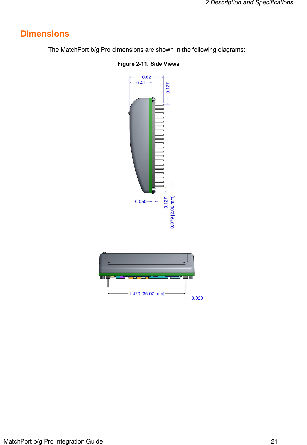
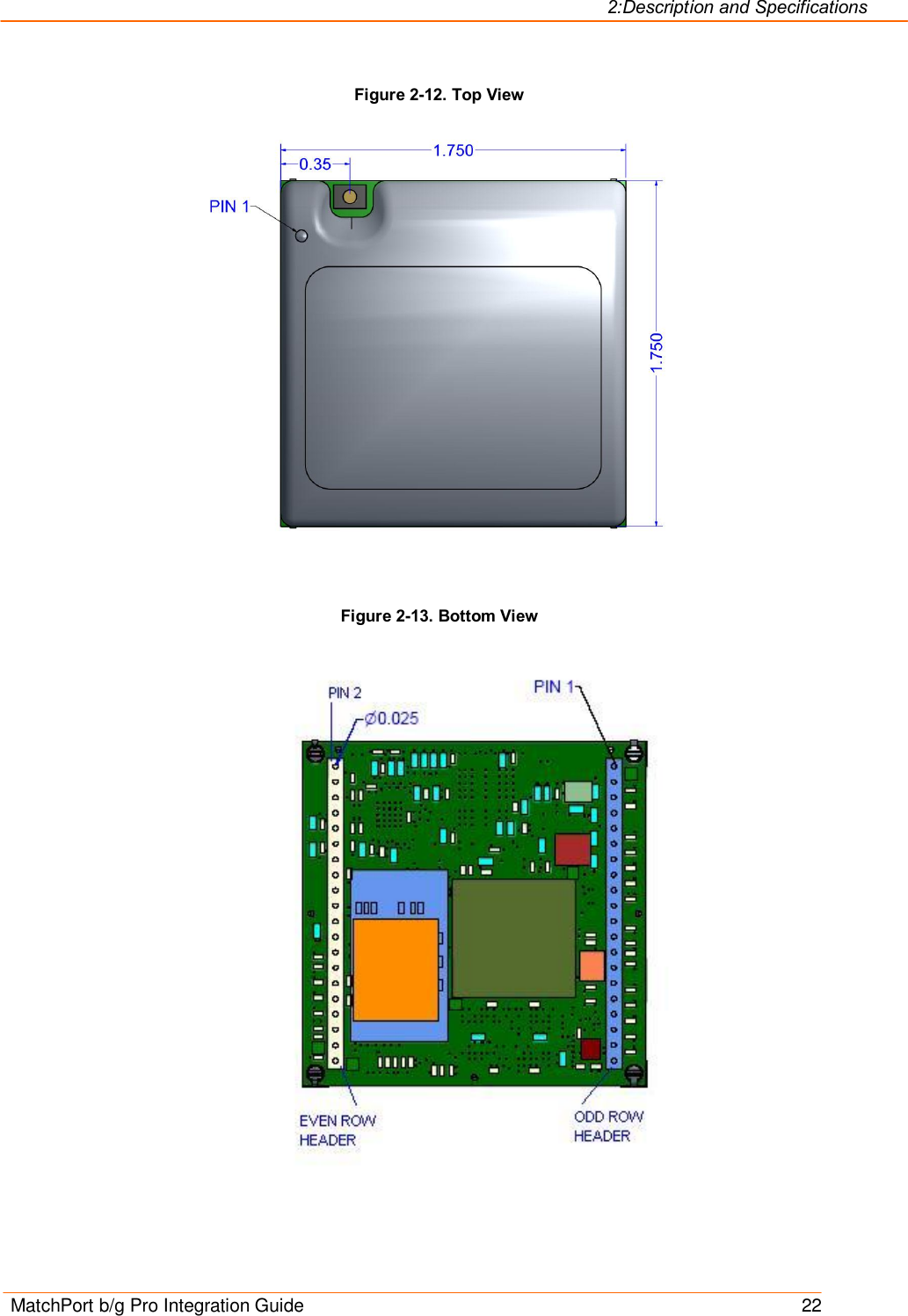
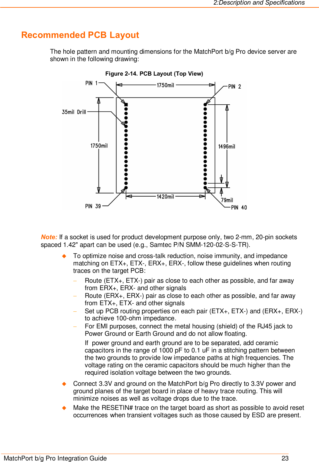
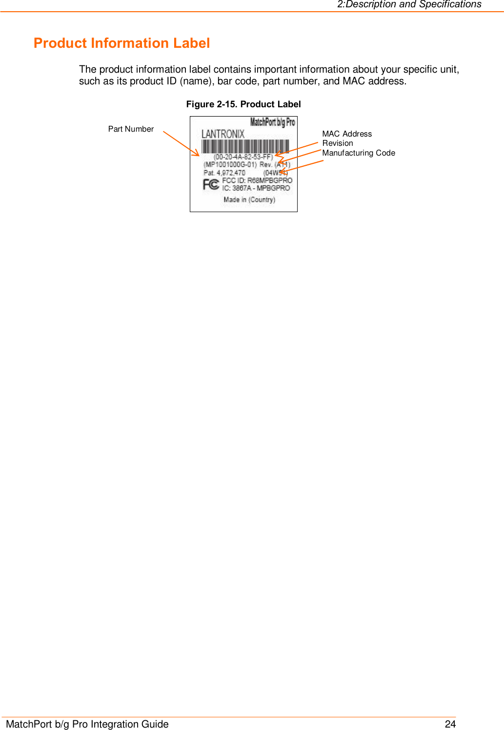
Integration Guide
Navigation menu
Upload a User Manual
Namespaces
Wiki Guide
HTML
PDF
Info
Views
User Manual
Discussion / Help
Navigation