lantronix MPBGPRO Wireless Device Server User Manual Integration Guide
lantronix Wireless Device Server Integration Guide
Integration Guide

Need new photo and logo
2/18/2008 4:38 PM
MatchPort b/g Pro™
Integration Guide
Part Number 900-532
Revision A ??? 2008

MatchPort b/g Pro Integration Guide 2
Copyright and Trademark
© 2008 Lantronix. All rights reserved. No part of the contents of this book may be
transmitted or reproduced in any form or by any means without the written permission of
Lantronix. Printed in the United States of America.
MatchPort® b/g Pro, with its patent-pending technology, is a trademark of Lantronix.
Ethernet is a trademark of XEROX Corporation. UNIX is a registered trademark of The
Open Group. Windows 95, Windows 98, Windows 2000, Windows NT, and Windows XP
are trademarks of Microsoft Corp. Netscape is a trademark of Netscape Communications
Corporation.
Contacts
Lantronix Corporate Headquarters
15353 Barranca Parkway
Irvine, CA 92618, USA
Phone: 949-453-3990
Fax: 949-453-3995
Technical Support
Online: www.lantronix.com/support
Sales Offices
For a current list of our domestic and international sales offices, go to the Lantronix web
site at www.lantronix.com/about/contact/

MatchPort b/g Pro Integration Guide 3
Disclaimer and Revisions
Operation of this equipment in a residential area is likely to cause interference to other
devices, in which case the user, at his or her own expense, will be required to take
whatever measures may be required to correct the interference.
Note: This product has been designed to comply with the limits for a Class B
digital device pursuant to Part 15 of FCC and EN55022:1998 Rules when
properly enclosed and grounded. These limits are designed to provide
reasonable protection against radio interference in a residential installation. This
equipment generates, uses, and can radiate radio frequency energy, and if not
installed and used in accordance with this guide, may cause interference to radio
communications.
Changes or modifications to this device not explicitly approved by Lantronix will void the
user's authority to operate this device.
Note: With the purchase of MatchPort b/g Pro, the OEM agrees to an OEM
firmware license agreement that grants the OEM a non-exclusive, royalty-free
firmware license to use and distribute the binary firmware image provided, only to
the extent necessary to use the MatchPort b/g Pro hardware. For further details,
please see the MatchPort b/g Pro OEM firmware license agreement.
Disclaimer
This equipment has been tested and found to comply with the limits for a Class B digital
device, pursuant to Part 15 of the FCC Rules. These limits are designed to provide
reasonable protection against harmful interference in a residential installation. This
equipment generates, uses, and can radiate radio frequency energy and, if not installed
and used in accordance with the instructions, may cause harmful interference to radio
communications. However, there is no guarantee that interference will not occur in a
particular installation. If this equipment does cause harmful interference to radio or
television reception, which can be determined by turning the equipment off and on, the
user is encouraged to try to correct the interference by one of the following measures:
u Reorient or relocate the receiving antenna.
u Increase the separation between the equipment and receiver.
u Connect the equipment into an outlet on a circuit different from that to which the
receiver is connected.
u Consult the dealer or an experienced radio/TV technician for help.
This device complies with Part 15 of the FCC Rules. Operation is subject to the following
two conditions: (1) This device may not cause harmful interference, and (2) this device
must accept any interference received, including interference that may cause undesired
operation.
This device is intended only for OEM Integrators. The OEM integrator should be aware of
the following important issues.
Labeling of the End Product
The label on the end product incorporating the MatchPort b/g pro module must clearly
state that it contains an FCC-approved RF module. For example: “This product contains
an RF transmitter FCC ID: R68MPBGPRO and IC: 3867A-MPBGPRO.”

MatchPort b/g Pro Integration Guide 4
RSS-GEN Sections 7.1.4 and 7.1.5 Statement for Devices with Detachable Antennas
This device has been designed to operate with the antennas listed in the Certificate, and
having a maximum gain of 5 dBi. Antennas not included in this list or having a gain
greater than 5 dBi are strictly prohibited for use with this device, unless system-level FCC
approval is gained. The required antenna impedance is 50 ohms.
To reduce potential radio interference to other users, the antenna type and its gain
should be so chosen that the equivalent isotropically radiated power (EIRP) is not more
than that required for successful communication.
Integration Note
a) This module is authorized under limited module approval specified to mobile host
equipment. So, the antenna must be installed such that 20cm is maintained between the
antenna and users.
b) The transmitter module may not be co-located with any other transmitter or antenna.
As long as the two conditions above are met, further transmitter testing will not be
required. However, the OEM integrator is still responsible for testing their end product for
any additional compliance requirements required with this module installed (for example,
digital device emission, PC peripheral requirements, etc.)
Note: In the event that these conditions cannot be met (for example certain
laptop configurations, general purpose PCMCIA or similar cards, or co-location
with another transmitter), then the FCC authorization is no longer considered
valid and the FCC ID cannot be used on the final product (including the
transmitter) and obtaining a separate FCC authorization.
Note: Changes or modifications to this device not explicitly approved by Lantronix will
void the user's authority to operate this device.
Date
Rev.
Comments
??? A Initial Release

MatchPort b/g Pro Integration Guide 5
Contents
1: Introduction 7
About the Integration Guide _______________________________________________ 7
Additional Documentation _________________________________________________ 7
2: Description and Specifications 8
MatchPort b/g Pro Block Diagram ___________________________________________ 8
MatchPort b/g Pro Pinouts________________________________ ____________________ 10
Power and Ground _____________________________________________________ 10
Reset ________________________________________________________________ 10
Ethernet Connections ___________________________________________________ 11
Ethernet LED Connections _______________________________________________ 12
Wireless LED Connections _______________________________________________ 13
Antenna Mating Connector _______________________________________________ 13
Antenna ______________________________________________________________ 14
Serial Input/Output _____________________________________________________ 14
Sample Layouts for RS485 Connectivity ____________________________________ 15
IO Configurable Pins (CPs) _______________________________________________ 17
BOOTP_EN# __________________________________________________________ 17
BOOTP enable ________________________________ ____________________________ 17
Diagnostics LED ________________________________ ___________________________ 17
Pin Connection Options ________________________________ ______________________ 18
Electrical Specifications _________________________________________________ 18
Wireless Specifications __________________________________________________ 19
Technical Specifications _________________________________________________ 20
Dimensions ___________________________________________________________ 21
Recommended PCB Layout ______________________________________________ 23
Product Information Label ________________________________________________ 24
3: Demonstration Kit 25
Contents of the Kit______________________________________________________ 25
Demo Board Description _________________________________________________ 25
Serial Interfaces _______________________________________________________ 26
Power Supply _________________________________________________________ 26
General Control ________________________________________________________ 26
Configuration Switch Bank _______________________________________________ 27
Demo Board Layout ____________________________________________________ 29
Demo Board Schematics ________________________________________________ 30
Compliance Information _________________________________________________ 34
Warranty _____________________________________________________________ 35
List of Figures

MatchPort b/g Pro Integration Guide 6
Figure 2-1. MatchPort b/g Pro Top and Front Views .................. Error! Bookmark not defined.
Figure 2-2. MatchPort b/g Pro Block Diagram .......................................................................... 9
Figure 2-3. Connection Diagram to an RJ45 Jack .................................................................. 12
Figure 2-4. Recommended LED Connections ........................................................................ 12
Figure 2-5. Combined RS232/422 Transceiver....................................................................... 15
Figure 2-6. Separate RS232/422 Transceivers....................................................................... 16
Figure 2-7. Separate RS422 Transceivers for 2-Wire and 4-Wire Setups ............................... 16
Figure 2-8. BOOTP_EN# APPLICATION CIRCUIT ................................................................ 18
Figure 2-9. Side Views ........................................................................................................... 21
Figure 2-10. Top View ........................................................................................................... 22
Figure 2-11. Bottom View ...................................................................................................... 22
Figure 2-12. PCB Layout (Top View) ...................................................................................... 23
Figure 2-13. Product Label .................................................................................................... 24
Figure 3-1. MatchPort Demo Board Layout ............................................................................ 29
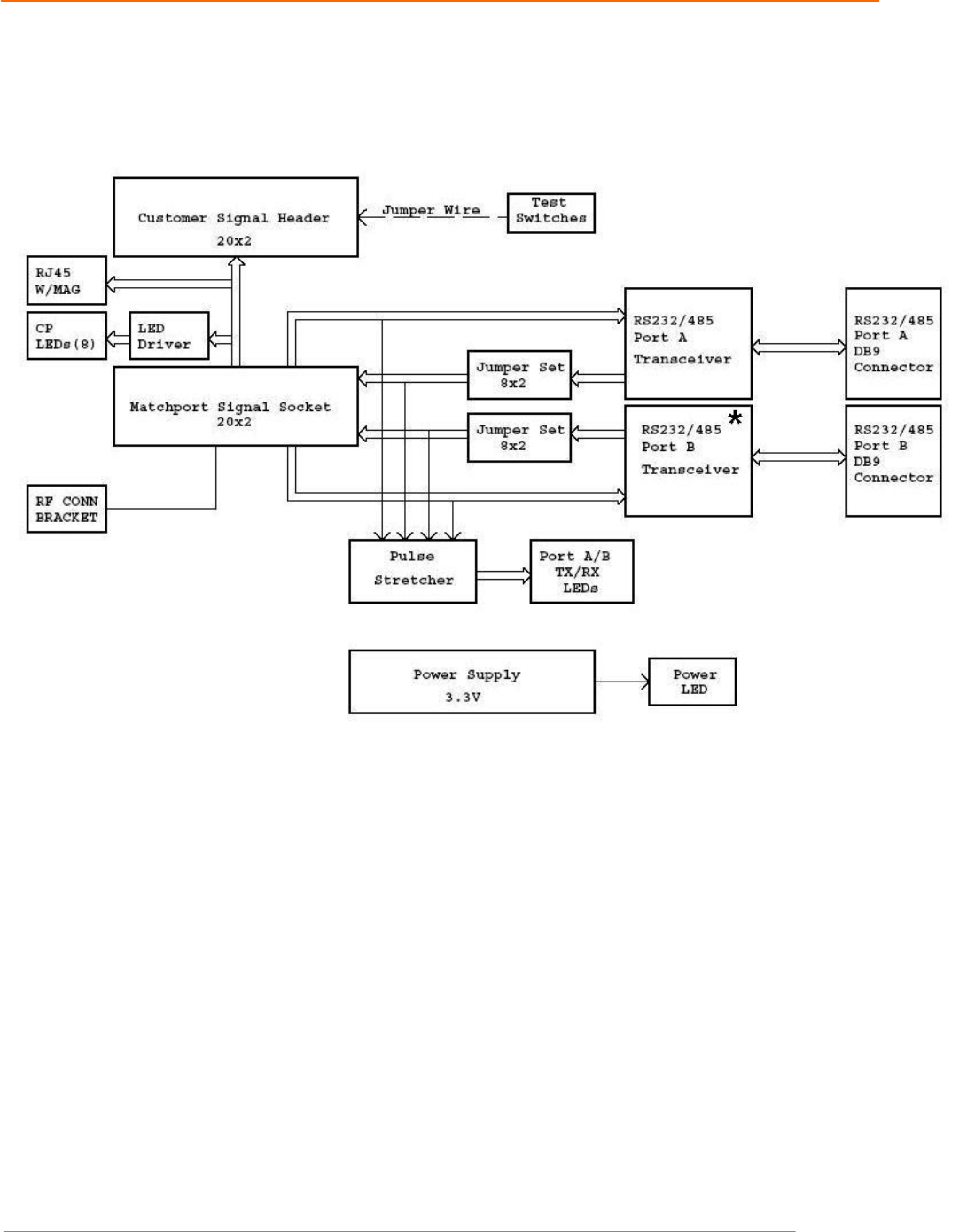
Figure 3-2. Demo Board Block Diagram ................................................................................. 30
Figure 3-3. Schematic............................................................................................................ 31
List of Tables
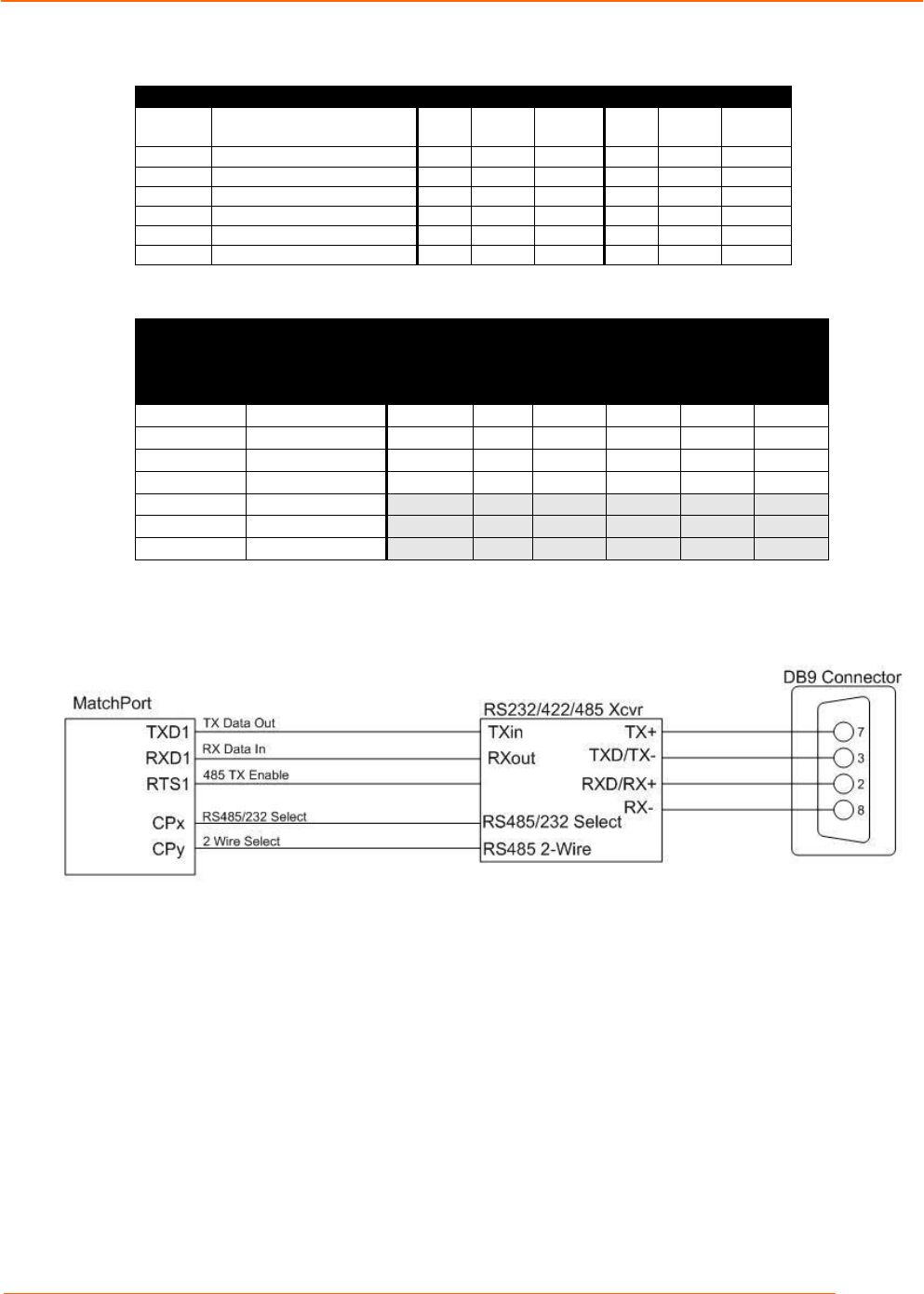
Table 2-1. RS232 Connections .............................................................................................. 15
Table 2-2. JP6 RS422/485 Connections on Demo board ....................................................... 15
Table 2-3. Absolute Maximum Ratings ................................................................................... 18
Table 2-4. Recommended Operating Conditions .................................................................... 19
Table 2-5. Specifications....................................................................................................... 20
Table 3-1. RS-232 Signals on Serial Port 1 ............................................................................ 26
Table 3-2. RS-422 4-Wire Connector on Serial Port 1 ............................................................ 26
Table 3-3. Demo Board JP1 Jumper Configuration ................................................................ 27
Table 3-4. Demo Board JP7 Jumper Configuration for CON1 ................................................. 27
Table 3-5. Demo Board JP5 Jumper Configuration ................................................................ 28

MatchPort b/g Pro Integration Guide 7
1
1:
:
I
In
nt
tr
ro
od
du
uc
ct
ti
io
on
n
About the Integration Guide
This guide provides the information needed to integrate the MatchPort b/g Pro™ device
server within another product. The intended audiences are the engineers responsible for
integrating the MatchPort b/g Pro into their product.
Notes:
u The MatchPort b/g Pro Demo Kit provides hardware and firmware for customer
evaluation. The complete kit includes a Module Universal Demo Kit (Lantronix
PN MP10010NMK-01) and a MatchPort b/g Pro sample (Lantronix PN
FP300200S-01)
u For developing application firmware on MatchPort b/g Pro, there is a MatchPort
Plus Development board with a Background Debug Mode (BDM) connector.
Please contact Lantronix for more details.
Additional Documentation
The following guides are available on the product CD and the Lantronix Web site
(www.lantronix.com)
MatchPort b/g Pro User
Guide
Provides information needed to configure, use,
and update the MatchPort b/g Pro firmware.
MatchPort b/g Pro
Command Reference
Lists and explains MatchPort b/g Pro command
line and XML commands.
MatchPort b/g Pro Quick
Start
Briefly explains the basics to get the MatchPort
b/g Pro up and running.
MatchPort Demonstration
Kit Quick Start Guide
Provides information needed to configure, use,
and update the MatchPort demonstration kit.

MatchPort b/g Pro Integration Guide 8
2
2:
:
D
De
es
sc
cr
ri
ip
pt
ti
io
on
n
a
an
nd
d
S
Sp
pe
ec
ci
if
fi
ic
ca
at
ti
io
on
ns
s
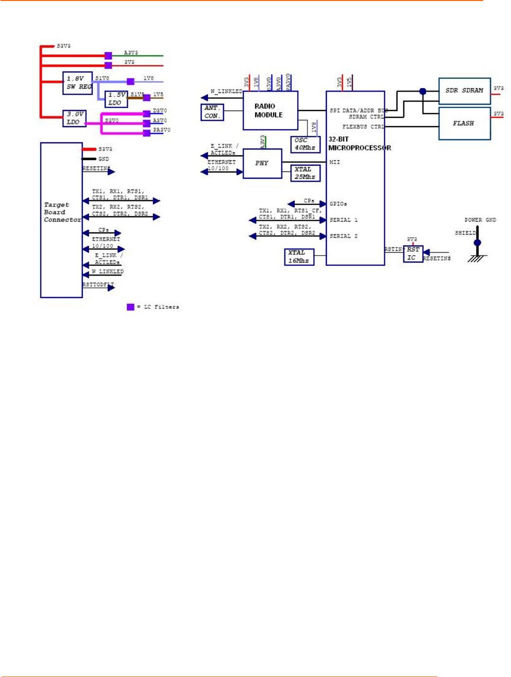
The MatchPort b/g Pro embedded device server is a complete network-enabling solution
on a 1.75"x1.75" PCB. This miniature device server empowers original equipment
manufacturers (OEMs) to go to market quickly and easily with networking and web page
serving capabilities built into their products.
The MatchPort b/g Pro has the following features:
u Power Supply: Regulated 3.3V input required. There are step-down converters
to 1.8V and 1.5V for ICs on board. All voltages have LC filtering to minimize
noises and emissions.
u Controller: A Lantronix DSTni-FX 32-bit microprocessor, running at 166 MHz
internal bus and 83 MHz external bus.
u Memory: 64 Mbits Flash and 64 Mbits SDRAM.
u Ethernet: 10/100 Base TX with auto-negotiation and HP auto-MDIX. On- board
100-ohm terminations included. Users just need an RJ45 jack and 1:1 Ethernet
magnetics with a minimal numbers of discrete components.
u Integrated Ethernet LED Drivers: For connections to Ethernet Link and
Activities LEDs.
u Serial Ports: Two full RS232 serial ports with all hardware handshaking signals.
Baud rates can be standard or customized up to 230 Kbps. RS232/422/RS485
functionalities can also be configured on Serial Port 1.
u Configurable IO Pins (CPs): Up to 7 pins are configurable as general purpose
I/Os if no DTR or DCD is used on serial ports.
u Interface Signals: 3.3V-level interface signals.
u Temperature Range: Operates over an extended temperature range.
MatchPort b/g Pro Block Diagram
The following drawing is a block diagram of the MatchPort b/g Pro showing the
relationships of the components.
2:Description and Specifications
MatchPort b/g Pro Integration Guide 9
Figure 2-1. MatchPort b/g Pro Block Diagram

2:Description and Specifications
MatchPort b/g Pro Integration Guide 10
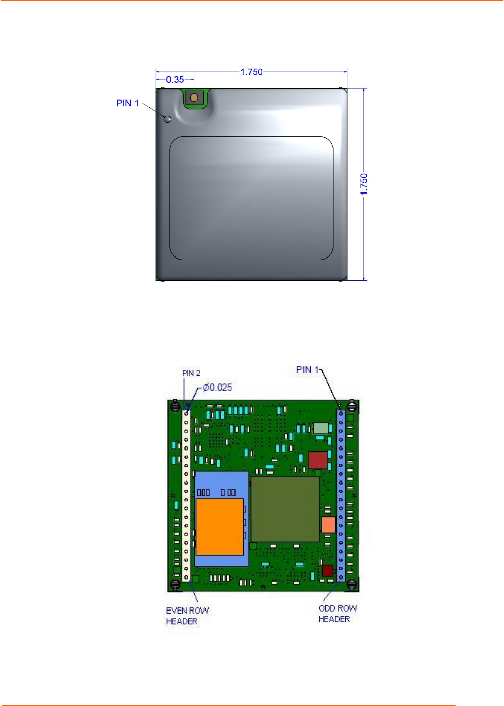
MatchPort b/g Pro Pinouts
There are two headers of 1x20, 2-mm pin spacing. The odd row header is designated as P1; pins
are numbered 1 to 39. The even row header is designated as P2; pins are numbered
2 to 40.
PIN
#
NAME
FUNCTION
PIN
#
NAME
FUNCTION
P1.1 RESETIN# Active low Reset. Leave
floating if not used. P2.2 GND Ground
P1.3 RSVD Reserved. Do not connect P2.4 NC No Connect
P1.5 TX1 Transmit Data output (logic
level), port 1 P2.6 ETX+ PHY’s Differential Ethernet
Transmit Data +
P1.7 RTS1 Request to Send output
(logic level), port 1 P2.8 ETX- PHY’s Differential Ethernet
Transmit Data -
P1.9 RX1 Receive Data input (logic
level), port 1 P2.10 ETCT Differential Ethernet Transmit
Data Center Tap
P1.11 CTS1 Clear to Send input (logic
level), port 1 P2.12 ERCT Differential Ethernet Receive
Data Center Tap
P1.13 CP1 IO Configurable Pin 1 P2.14 ERX+ PHY’s Differential Ethernet
Receive Data +
P1.15 CP2 IO Configurable Pin 2 P2.16 ERX- PHY’s Differential Ethernet
Receive Data -
P1.17 CP3 IO Configurable Pin 3 P2.18 E_LINKLED Connect to Link LED. 3.3V
level. Active low.
P1.19 CP4 IO Configurable Pin 4 P2.20 E_ACTLED Connect to Acitivities LED. 3.3V
level. Active low.
P1.21 TX2 Transmit Data output (logic
level), port 2 P2.22 W_LINKLED Wireless LAN status LED output
Active low
P1.23 RTS2 Request to Send output
(logic level), port 2 P2.24 BOOTP_EN# Network Boot and Boot Loader
Enable pin.
P1.25 RX2 Receive Data input (logic
level), port 2 P2.26 RSVD Reserved. Do not connect
P1.27 CTS2 Clear to Send input (logic
level), port 2 P2.28 RSVD Reserved. Do not connect
P1.29 CP5 IO Configurable Pin 5 P2.30 RSVD Reserved. Do not connect
P1.31 CP6 IO Configurable Pin 6 P2.32 RSVD Reserved. Do not connect
P1.33 CP7 IO Configurable Pin 7 P2.34 RSVD Reserved. Do not connect
P1.35 RSVD Reserved. Do not connect P2.36 RSVD Reserved. Do not connect
P1.37 S3.3V 3.3V Power Input P2.38 RSVD Reserved. Do not connect
P1.39 GND Ground P2.40 RSVD Reserved. Do not connect
Power and Ground
The MatchPort b/g Pro requires a regulated 3.3Vdc +/- 5% power input at P1.37 and
ground at pin P1.39.
Direct connection of 3.3V and ground on MatchPort b/g Pro to 3.3V power and ground
planes of the target board is recommended in place of heavy trace routing to minimize
noises as well as voltage drops at the connection.
Reset
The MatchPort b/g Pro reset pin RESETIN# is an input-only pin and connects to an 811-
type reset IC. This input is for a pushbutton switch type manual reset. If no external reset
control is desired, leave this pin floating.

2:Description and Specifications
MatchPort b/g Pro Integration Guide 11
There is an on board capacitor, 0.1uF to ground, at the RESETIN# to filter out transient
voltages. However, as always, it is a good practice to have RESETIN# trace on the target
board as short as possible to avoid reset occurrences when transient voltages such as
those caused by ESD are present.
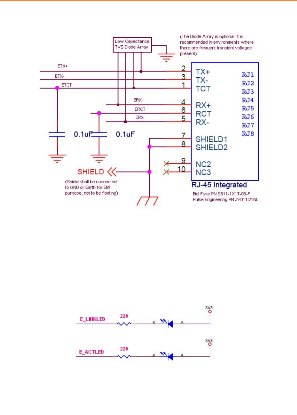
Ethernet Connections
The MatchPort b/g Pro provides Ethernet interface transmit ETX and receive data ERX
connections from a PHY device. Thus, before presenting signals to the outside world
using an RJ45 jack, a 1:1 Ethernet Magnetics is needed to interface and to isolate the
unit. A recommended connection diagram to an RJ45 jack with integrated 1:1 Ethernet
magnetics is shown below.
2:Description and Specifications
MatchPort b/g Pro Integration Guide 12
Figure 2-2. Connection Diagram to an RJ45 Jack
We recommend a low capacitance TVS diode array such as a Semtech SRV05-4 at
ETX+, ETX-, ERX+, ERX- if frequent transient voltages are present.
Ethernet LED Connections
The E_LINKLED and E_ACTLED signals are driven by the PHY. They are active low.
Recommended connections on the target board are shown below.
Figure 2-3. Recommended LED Connections
2:Description and Specifications
MatchPort b/g Pro Integration Guide 13
Warning: The MatchPort b/g Pro has two 4.7K pull-ups on the E_LINKLED
and E_ACTLED signals to set up the PHY’s LED Indicator Mode as Ethernet
Link and Activities at Power On Reset (POR). Do not connect these two
signals with any pull-down resistors as they may corrupt the logic level on
these two signals at POR, causing undesired operation.
Wireless LED Connections
The W_LINKLED is driven by the Radio Module. It is active low. Recommended
connections on the target board are shown below.
Figure TBD. Recommended LED Connections
Output W_LINKLED can be used to drive an external LED to monitor the activity
of the radio. The output is active when the receiver and or transmitter are on. The
output is active low and can drive an LED with 10mA max.
If WLAN Power Management is disabled, and when the unit is associated with a network,
the receiver will always be on and thus any LED output, that indicates the receiver or
transmitter being on will be active continuously.
Antenna Mating Connector
An antenna connection is made via the U.FL style connector on the MatchPort. Lantronix
offers two cable options, reverse-SMA to U.FL (P/N 500-180-R) or U.FL to U.FL (P/N
500-181-R).
Figure 2-4. Reverse-SMA to U.FL (P/N 500-180-R)
Figure 2-5. U.FL to U.FL Cable (P/N 500-181-R)
2:Description and Specifications
MatchPort b/g Pro Integration Guide 14
Note: The antenna cable is included in the MatchPort b/g Pro sample. For
production, it can be purchased from Lantronix or a cable supplier.
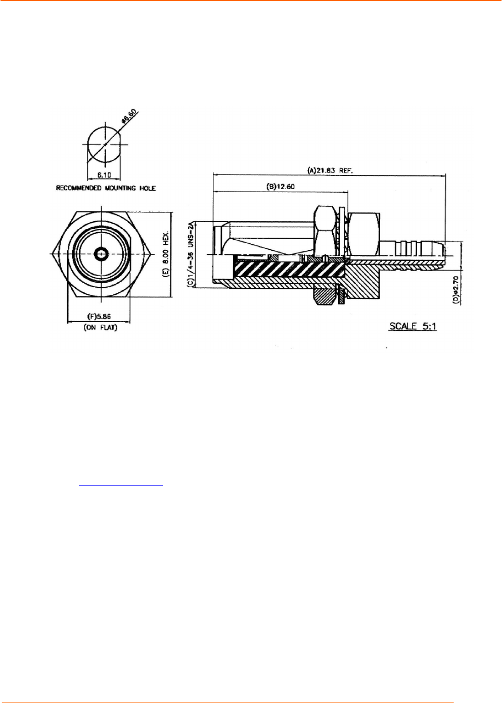
Figure 2-6. R-SMA Antenna Connector Dimensions (not to scale)
Antenna
The MatchPort b/g Pro has been FCC certified with a 5dBi gain antenna for wireless
802.11b/g. It is for applications with antennas of equal gain or less. The following are two
of the recommended antennas with 2.15dBi gain and a link to their vendor. They are
available from Lantronix as well.
u Wanshih WSS003 (Lantronix part number 930-029-R)
u Wanshih WSS002 (Lantronix part number 930-033-R)
www.wanshih.com
Serial Input/Output
The unit has two serial ports compatible with RS232 serial standards at data rates up to
230 Kbps. Serial Port 1 can also be configured as RS422/485, but Serial Port 2 cannot.
The serial I/O signals are 3.3V CMOS logic level. Serial signals can be connected to the
OEM CPU/UART or RS232/422/485 serial transceivers. For evaluation and prototype
work, it is convenient to have an external RS232 interface that can connect to the serial
port on a PC. The MatchPort Demo Board has RS232/422/485 transceivers to implement
this external interface. If desired, use the CPs to create a DTE or DCE-style interface
using any available CPs. To create these interfaces, connect the signals according to the
tables below.
Note: CPx and CPy are any of the available CPs.
2:Description and Specifications
MatchPort b/g Pro Integration Guide 15
Table 2-1. RS232 Connections
MatchPort b/g Pro
DCE Connector
DTE Connector
Signal
(Logic)
Description
DB9
DB25
Signal
DB9
DB
25
Signal
RXD1 Data In 2 3 RXD1 3 2 TXD1
TXD1 Data Out 3 2 TXD1 2 3 RXD1
RTS1 H/W Flow Control Output
7 4 RTS1 8 5 CTS1
CTS1 H/W Flow Control Input 8 5 CTS1 7 4 RTS1
CPx Modem Control Input 1 8 DCD 4 20 DTR
CPy Modem Control Output 4 20 DTR 1 8 DCD
Table 2-2. JP6 RS422/485 Connections on Demo board
MatchPort
b/g Pro
Signal
(logic)
Description
RS485
Signal
JP6
Pin
DB25
4
Wire
DB25
2
Wire
DB9
4 wire
DB9
2 wire
TXD1 Data Out TX+485 4 14 14 7 7
TXD1 Data Out TX-485 3 15 15 3 3
RXD1 Data In RX+485 2 21 14 2 7
RXD1 Data In RX-485 1 22 15 8 3
RTS1 TX Enable
CP3 RS485 Select
CP4 RS485 2-wire
Sample Layouts for RS485 Connectivity
Figure 2-7. Combined RS232/422 Transceiver
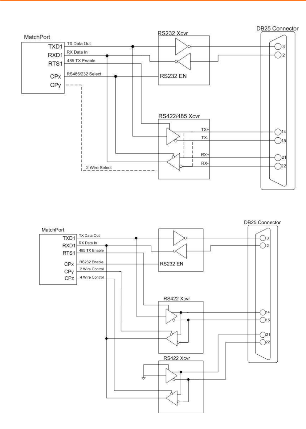
2:Description and Specifications
MatchPort b/g Pro Integration Guide 16
Figure 2-8. Separate RS232/422 Transceivers
Figure 2-9. Separate RS422 Transceivers for 2-Wire and 4-Wire Setups

2:Description and Specifications
MatchPort b/g Pro Integration Guide 17
To protect the MatchPort b/g Pro and circuitry on the target board against ESD at serial
ports, the selected transceiver(s) should have RS232/422/485 bus-pin ESD protection
(typically around 15 KV) either on-chip or by external diode arrays.
IO Configurable Pins (CPs)
There are up to seven CPs if no DTR or DCD is used on the serial ports. Any CP can be
configured as DTR or DCD as described above. CPs can be configured (see the User
Guide). All CPs have a pull-up.
PIN #
NAME
FUNCTION
P1.13 CP1 IO Configurable Pin 1
P1.15 CP2 IO Configurable Pin 2
P1.17 CP3 IO Configurable Pin 3
P1.19 CP4 IO Configurable Pin 4
P1.29 CP5 IO Configurable Pin 5
P1.31 CP6 IO Configurable Pin 6
P1.33 CP7 IO Configurable Pin 7
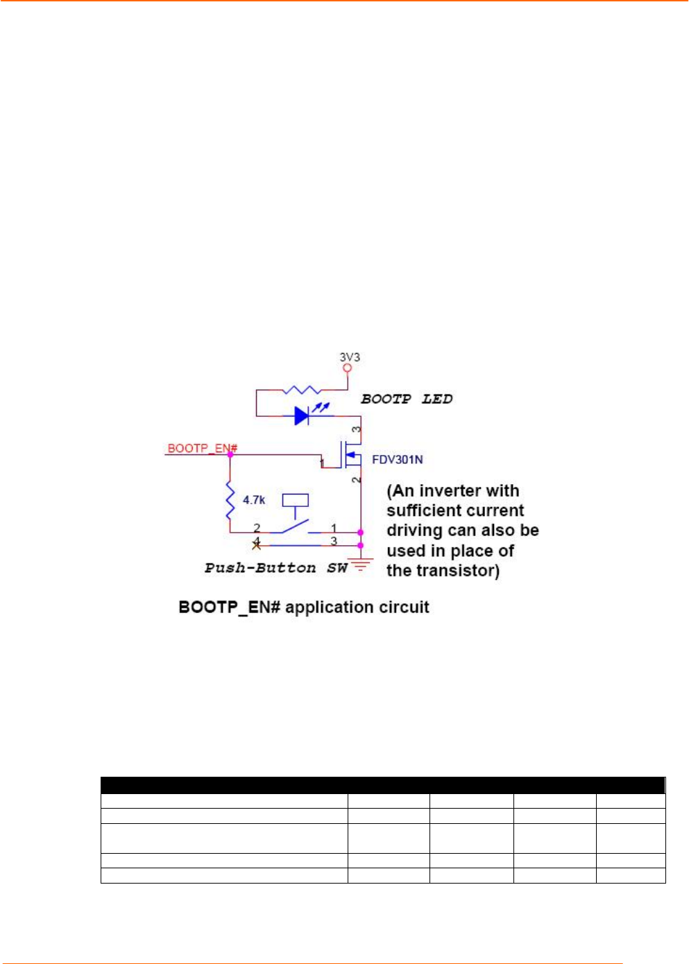
BOOTP_EN#
The BOOTP_EN# pin performs two functions simultaneously. It drives an optional
external diagnostics LED to indicate the status of the bootloader. It also serves as input
to enable booting from the network when no valid FW image is found in FLASH.
BOOTP enable
Holding BOOTP_EN# low (via switch or jumper) during and up to 10 seconds after a
reset allows booting the device with a FW image on a TFTP server only in case no valid
image is present on FLASH.
The MatchPort b/g Pro will issue a BOOTP request to acquire an IP address for itself, the
IP address of a TFTP server, and the filename of the FW image on the TFTP server.
Then it will fetch that file via TFTP, verify, and execute it.
Diagnostics LED
After supplying power to the unit or pressing and releasing the reset button, the
diagnostics LED turns on and stays on while the bootloader is running and does not
encounter any errors. After the bootloader loads firmware from serial, network or FLASH,
it turns off the LED right before handing over execution.
In case an error occurs during the bootloader operation, it will flash the LED. The pattern
will be pause, X * long flashes, Y * short flashes, pause, X long flashes, etc.
X is the first digit of the error number and Y the second.
Following are the currently implemented errors:
INVALID_BOOTLOADER_CHECKSUM 11
NO_FLASH_IMAGE_FOUND 12
BAD_FLASH_IMAGE_FOUND 13
BAD_COMMAND_PARAMETER 14
NO_BOOTP_RESPONSE 15
BAD_BOOTP_RESPONSE 16
NO_BOOTP_TFTP_IMAGE 17
RECEPTION_TIMEOUT 18
RECEPTION_OVERRUN 19
2:Description and Specifications
MatchPort b/g Pro Integration Guide 18
IMAGE_OVERSIZE 21
BAD_IMAGE_CHECKSUM 22
BAD_IMAGE_DESTINATION 23
INTERNAL_CODING_PROBLEM 24
Pin Connection Options
The circuit below is an example on how to correctly connect a switch (or permanent
jumper) and an LED to the BOOTP_EN# pin. The customer has the option of
implementing either the switch/resistor or the driver/LED or both or none.
The switch can be replaced by a jumper or hardwire. Having the hardwire in place means
that if the firmware image in FLASH becomes corrupt, the MatchPort b/g Pro will
automatically send out BOOTP requests over the network. This could be a security risk.
The switch or jumper allows BOOTP requests to be sent only after manual intervention.
If no switch/jumper/hardwire is installed, network recovery is only possible by issuing
a!NL command over the serial port.
Figure 2-10. BOOTP_EN# APPLICATION CIRCUIT
Electrical Specifications
Caution: Stressing the device above the rating listed in this table may cause
permanent damage to the MatchPort b/g Pro. Exposure to Absolute Maximum
Rating conditions for extended periods may affect the MatchPort b/g Pro's
reliability.
Table 2-3. Absolute Maximum Ratings
Parameter
Symbol
Min
Max
Units
Supply Voltage VCC 0 3.6 Vdc
CP Voltage VCP -0.3 VCC +0.05 Vdc
Ethernet ETX+, ETX-, ERX+, ERX-
Voltage VETH 0 VCC +0.3 Vdc
Operating Temperature -40 70 oC
Storage Temperature -40 85 oC
2:Description and Specifications
MatchPort b/g Pro Integration Guide 19
Table 2-4. Recommended Operating Conditions
Parameter
Symbol
Min
Typical
Max
Units
Supply Voltage VCC 3.15 3.3 3.46 Vdc
Supply Voltage Ripples VCC_PP 2 %
Supply Current _ Power Management
enabled ICC 245 mA
Supply Current _ Power Management
disabled 260 mA
Supply Current (Peak) 350 mA
Supply Reset Threshold VRST 2.85 2.93 3.00 Vdc
CP Pull-ups, except CP5 RPU 100 Kohm
CP5 Pull-up RPU 20 Kohm
CP, RX, CTS, BOOTP_EN#
Input Low Voltage VCP_IL 0.8 Vdc
CP, RX, CTS, BOOTP_EN#
Input High Voltage VCP_IH 2 Vdc (see note
below)
CP, TX, RTS Output Low Voltage
(IOL = 4 mA) VCP_OL 0.4 Vdc
CP, TX, RTS Output High Voltage
(IOH = -4 mA) VCP_OH VCC -
0.4 Vdc (see note
below)
E_LINKLED, E_ACTLED
Current Drive (sink) IELED 12 mA (see note
below)
W_LINKLED 10 mA
Notes:
u Do not connect a pull-down resistor on E_LINKLED and E_ACTLED.
u All pins are not 5V-tolerant
Wireless Specifications
Refer to the following table for the MatchPort b/g Pro’s wireless specifications:
Table 2-5. Wireless Specifications
Category
IEEE 802.11b/g
Frequency Range 2.400 – 2.484 GHz
Output Power 14 +2.0/- 1.5 dBm 1, 2, 5.5, 11 Mbps
12 +/- 1.5 dBm 6, 9, ≥ 12 Mbps
Antenna Connector RF, U-FL TYPE
HIROSE PN = U_FL-R-SMT-10
Data Rates 1,2,5.5,11,6,9,12,18,24,36,48,54 Mbps
Radio Number of
Selectable
Subchannels
US 1-11
CA 1-11
JP 1-14
FR 10-13
SP 10-11
OT 1-13 (OT=Others)
Modulation DSSS,DBPSK,DQPSK,CCK, OFDM,
16QAM, 64QAM
Security WEP, WPA, WPA2/802.11i, EAP-
TTLS, PEAP, LEAP
Maximum Receive Level -10 dBm (with PER < 8%)

2:Description and Specifications
MatchPort b/g Pro Integration Guide 20
Receiver Sensitivity -69 dBm for 54 Mbps
-88 dBm for 11 Mbps
-85 dBm for 6 Mbps
-91 dBm for 1.0 Mbps
W_LINKLED Current Max 10 mA
Technical Specifications
Table 2-6. Specifications
Category
MatchPort b/g Pro
CPU Lantronix DSTni-FX 32-bit Microprocessor, 166 MHz internal bus,
83 MHz external bus
Memory 64 Mbits Flash and 64 Mbits SDRAM
Firmware Upgradeable via TFTP, FTP, and the Web
Configuration Pins Up to 7 pins if no DTR or DCD is used on serial ports.
Reset Circuit RESETIN# is low active and push-button type. Minimum RESETIN# pulse
width is 2 ms at IIL = -500 µA. Reset is also triggered if 3.3V at pin P1.37
drops below 2.93V typically.
Serial Interface CMOS (Asynchronous) 3.3V - level signals
Speed software selectable and customizable (300 bps to 230400 bps)
Serial Line Formats 7 or 8 data bits, 1-2 Stop bits, Parity: odd, even, none
Modem Control DTR, DCD using CPs
Flow Control XON/XOFF (software), CTS/RTS (hardware), none
Network Interface Ethernet 10/100 base TX with Auto Negotiation, and HP Auto MDIX
Protocols Supported ARP, UDP, TCP, Telnet, ICMP, SNMP, DHCP, BOOTP, Auto IP, HTTP,
HTTPS, SMTP, TFTP, FTP
Management Internal web server, SNMP
Serial login, Telnet login, DeviceInstaller software, SSH
Internal Web Server Serves web pages
WEB storage capacity: approx. 2.5 MB
Security Password protection, locking features
Average Power
Consumption (at
3.3V)
0.8 W with Power Management enabled
0.85 W with Power Management disabled
Weight 1 oz (28 g)
Cover Material ABS
Temperature Operating range: -40°C to +70°C (-40°F to +158°F)
Storage range: -40°C to +85°C (-40°F to 185°F)
Warranty 2-year limited warranty
Included Software Windows™ 98/NT/2000/XP-based Device Installer configuration software
and Windows™-based Com Port Redirector and Secure Com Port
Redirector, DeviceInstaller, and Web-Manager.
2:Description and Specifications
MatchPort b/g Pro Integration Guide 21
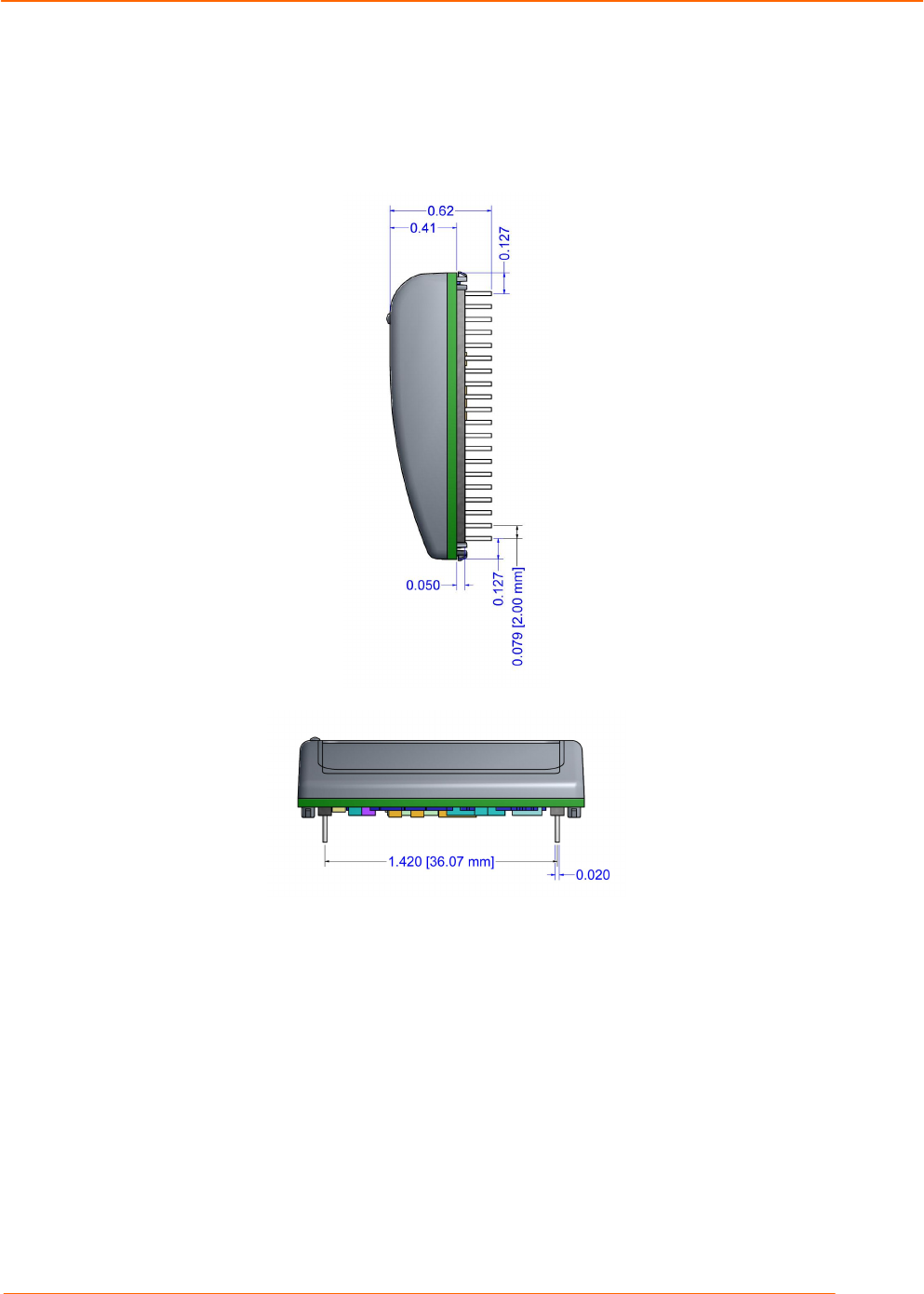
Dimensions
The MatchPort b/g Pro dimensions are shown in the following diagrams:
Figure 2-11. Side Views
2:Description and Specifications
MatchPort b/g Pro Integration Guide 22
Figure 2-12. Top View
Figure 2-13. Bottom View
2:Description and Specifications
MatchPort b/g Pro Integration Guide 23
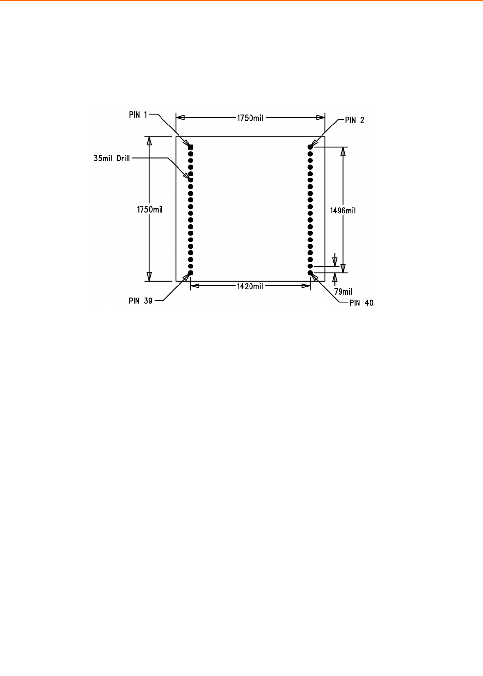
Recommended PCB Layout
The hole pattern and mounting dimensions for the MatchPort b/g Pro device server are
shown in the following drawing:
Figure 2-14. PCB Layout (Top View)
Note: If a socket is used for product development purpose only, two 2-mm, 20-pin sockets
spaced 1.42" apart can be used (e.g., Samtec P/N SMM-120-02-S-S-TR).
u To optimize noise and cross-talk reduction, noise immunity, and impedance
matching on ETX+, ETX-, ERX+, ERX-, follow these guidelines when routing
traces on the target PCB:
- Route (ETX+, ETX-) pair as close to each other as possible, and far away
from ERX+, ERX- and other signals
- Route (ERX+, ERX-) pair as close to each other as possible, and far away
from ETX+, ETX- and other signals
- Set up PCB routing properties on each pair (ETX+, ETX-) and (ERX+, ERX-)
to achieve 100-ohm impedance.
- For EMI purposes, connect the metal housing (shield) of the RJ45 jack to
Power Ground or Earth Ground and do not allow floating.
If power ground and earth ground are to be separated, add ceramic
capacitors in the range of 1000 pF to 0.1 uF in a stitching pattern between
the two grounds to provide low impedance paths at high frequencies. The
voltage rating on the ceramic capacitors should be much higher than the
required isolation voltage between the two grounds.
u Connect 3.3V and ground on the MatchPort b/g Pro directly to 3.3V power and
ground planes of the target board in place of heavy trace routing. This will
minimize noises as well as voltage drops due to the trace.
u Make the RESETIN# trace on the target board as short as possible to avoid reset
occurrences when transient voltages such as those caused by ESD are present.
2:Description and Specifications
MatchPort b/g Pro Integration Guide 24
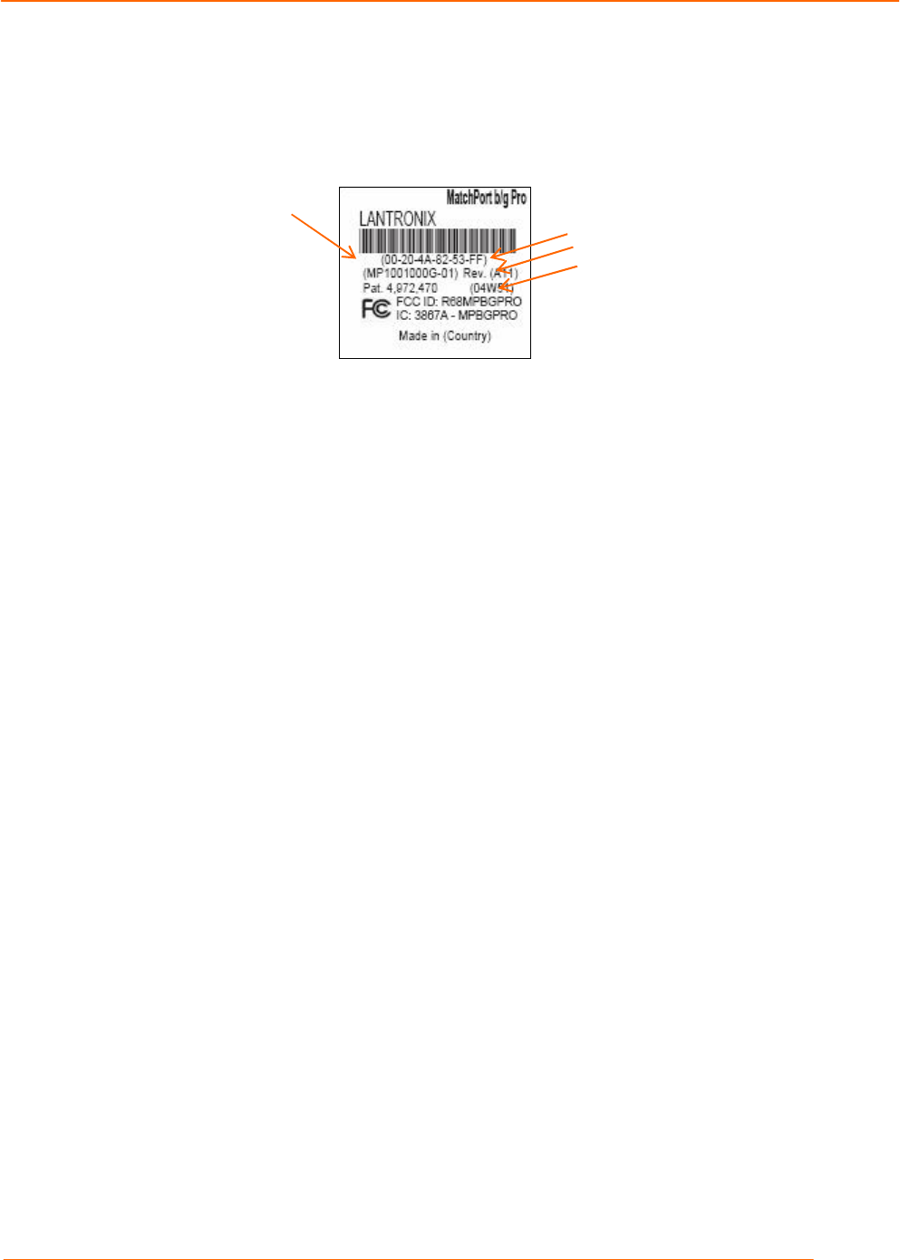
Product Information Label
The product information label contains important information about your specific unit,
such as its product ID (name), bar code, part number, and MAC address.
Figure 2-15. Product Label
MAC Address
Revision
Manufacturing Code
Part Number

MatchPort b/g Pro Integration Guide 25
3
3:
:
D
De
em
mo
on
ns
st
tr
ra
at
ti
io
on
n
K
Ki
it
t
Using a MatchPort b/g Pro sample and the MatchPort Demonstration Kit, you can get
familiar with the product and understand how to integrate the MatchPort b/g Pro into a
given product design.
Contents of the Kit
The MatchPort Demonstration Kit contains the following items:
u MatchPort Demo Board
u 3.3V wall adaptor
u RS-232 cable, DB9F/F, null modem
u RJ45 Ethernet cable
u Antenna 2.15 dBi gain
You must obtain a MatchPort b/g Pro sample separately for use with this
Demonstration Kit.
Note: For developing application firmware on the MatchPort b/g Pro, Lantronix
offers a MatchPort Plus Development board with a Background Debug Mode
(BDM) connector. Please contact Lantronix for more details.
Demo Board Description
The MatchPort Demo Board provides a test platform for the Lantronix MatchPort device
server products, including MatchPort b/g Pro. The demo board uses 3.3V power from the
wall adaptor same as that of MatchPort. The demo board has the following features
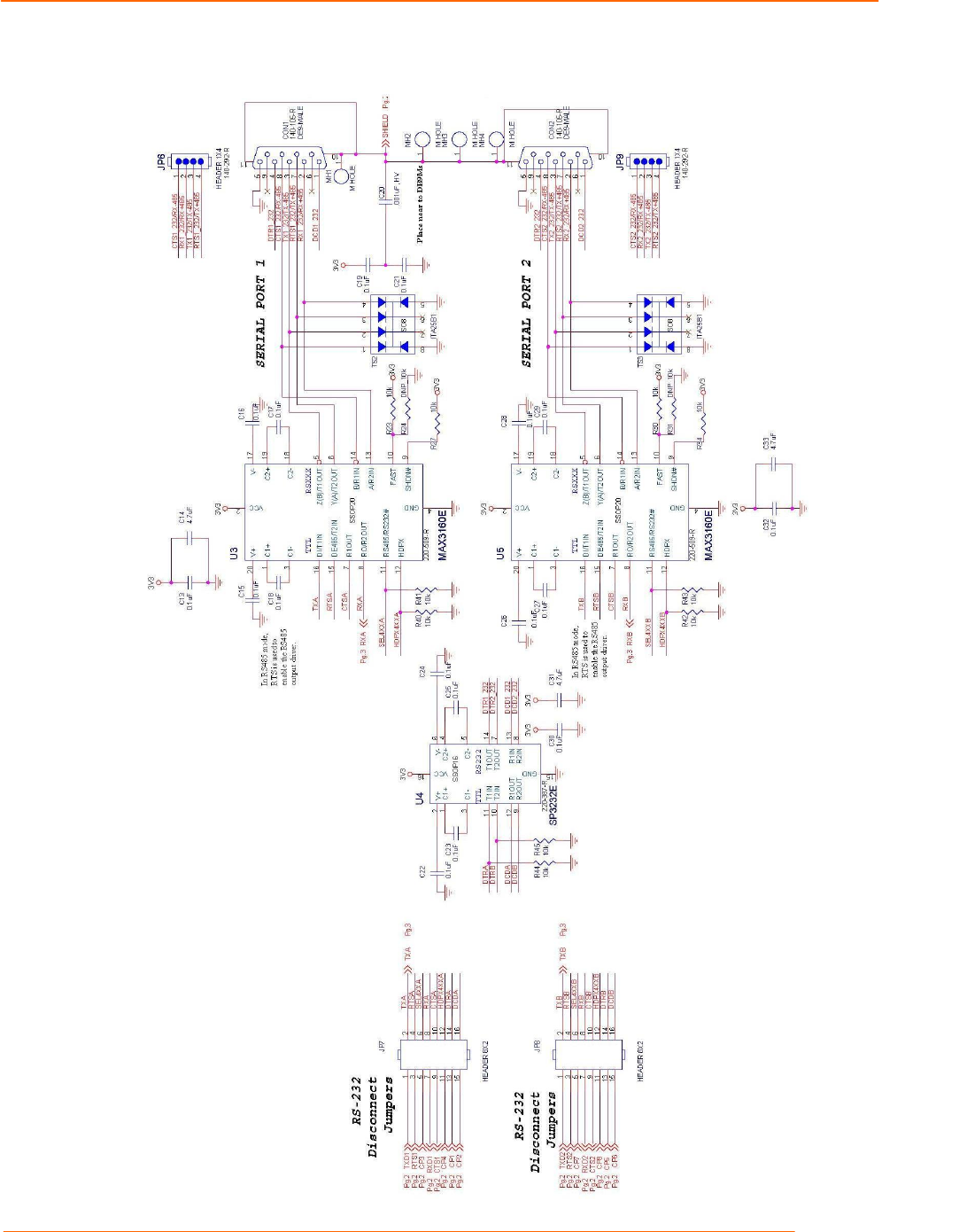
u 2 serial ports with an RS232/RS422/RS485 Maxim MAX3160 transceiver on
each. The ports have DB9M connectors CON1and CON2.
u 1 RJ45 with integrated magnetics 1:1 for Ethernet connection; auto-MDIX
compatible.
u Access to all signals on the MatchPort via header pins for measurements and
connections to other places.
3:Demonstration Kit
MatchPort b/g Pro Integration Guide 26
Serial Interfaces
The demo board has RS-232/422/485 transceivers, one per port. However, note that only
Serial Port 1 supports RS232/RS422/485 on MatchPort b/g Pro. The table below lists the
RS232 signals and corresponding pins on the demo board. All signals are level-shifted by
the transceivers.
Table 3-1. RS-232 Signals on Serial Port 1
MatchPort Demo
PIN FUNCTION
DB9
Pin #
Serial Port 1
CON1
TX1_232 (Data Out) 3
RX1_232 (Data In) 2
CTS1_232 (HW Flow Control Input) 8
RTS1_232 (HW Flow Control Output) 7
DCD1_232 (Modem Control Input) 1
DTR1_232 (Modem Control Output) 4
GND (Ground) 5
Table 3-x. RS-232 Signals on Serial Port 2
MatchPort Demo
PIN FUNCTION
DB9
Pin #
Serial Port 2
CON2
TX2_232 (Data Out) 3
RX2_232(Data In) 2
CTS2_232 (HW Flow Control Input) 8
RTS2_232 (HW Flow Control Output) 7
DCD2_232 (Modem Control Input) 1
DTR2_232 (Modem Control Output) 4
GND (Ground) 5
Table 3-2. RS-422 4-Wire Connector on Serial Port 1
MatchPort Demo
PIN FUNCTION
DB9
Pin #
Serial Port 1
CON1
TX+485 (Data Out) 7
TX-485 (Data Out) 3
RX+485 (Data In) 2
RX-485 (Data In) 8
GND (Ground) 5
Power Supply
The demo board uses an external 3.3V regulated supply (included with kit).
General Control
The following tables denote the configuration of the demo board. Configuring the jumpers
re-routes signals on the demo board to drive LEDs (general purpose outputs), to use as
Serial control signals, or to connect to other places on target board as General Purpose
IO (GPIO).
3:Demonstration Kit
MatchPort b/g Pro Integration Guide 27
Configuration Switch Bank
Table 3-3. Demo Board JP1 Jumper Configuration
JP1 pin/Signal
JP1 pin/Signal
Function
1/CP1 2/LED12 Jumper 1-2, CP1 Controls LED12
3/CP2 4/LED11 Jumper 3-4, CP2 Controls LED11
5/CP3 6/LED10 Jumper 5-6, CP3 Controls LED10
7/CP4 8/LED9 Jumper 7-8, CP4 Controls LED9
9/CP5 10/LED8 Jumper 9-10, CP5 Controls LED8
11/CP6 12/LED7 Jumper 11-12, CP6 Controls LED7
13/CP7 14/LED6 Jumper 13-14, CP7 Controls LED6
Table 3-4. Demo Board JP7 Jumper Configuration for CON1
JP7
pin/Signal
JP7
pin/Signal
Function
1/TXD1 2/TXA Jumper 1-2, Send TXD to RS232/485 transceiver.
3/RTS1 4/RTSA Jumper 3-4, Send RTS to RS232/485 transceiver. In 485 mode RTS
controls transmit enable.
5/CP3 6/SEL4XXA Jumper 5-6, CP3 high selects 485 mode, low 232 mode. Pin at
transceiver is pulled down to default to 232 mode.
7/RXD1 8/RXA Jumper 7-8, Receive RXD from RS232/485 transceiver.
9/CTS1 10/CTSA Jumper 9-10, Receive CTS from RS232 transceiver.
11/CP4 12/HDPX4XXA Jumper 11-12. In 485 mode, CP4 selects full duplex when low and half
duplex when high. Pin at transceiver is pulled down to default to full
duplex.
13/CP1 14/DTRA Jumper 13-14, CP1 drives DTR to RS232 transceiver.
15/CP2 16/DCDA Jumper 15-16, CP2 receives DCD from RS232 transceiver.
Table 3-xx. Demo Board JP8 Jumper Configuration for CON2
JP7
pin/Signal
JP7
pin/Signal
Function
1/TXD2 2/TXB Jumper 1-2, Send TXD to RS232 transceiver.
3/RTS2 4/RTSB Jumper 3-4, Send RTS to RS232 transceiver.
5/CP7 6/SEL4XXB Do
not
add jumper since only RS232 is supported. Pin at
transceiver is pulled down to default to 232 mode.
7/RXD2 8/RXB Jumper 7-8, Receive RXD from RS232 transceiver.
9/CTS2 10/CTSB Jumper 9-10, Receive CTS from RS232 transceiver.
11/RESERVED
on MatchPort
b/g Pro
12/HDPX4XXB Do
not
add jumper since only RS232 is supported. Pin at
transceiver is pulled down to default to 232 mode.
13/CP5 14/DTRB Jumper 13-14, CP5 drives DTR to RS232 transceiver.
15/CP6 16/DCDB Jumper 15-16, CP6 receives DCD from RS232
transceiver.
Note: CP arrangement in the tables above is for demonstration purpose only. In
customers’ applications, any CP can be assigned as a function of DTR or DCD.
All CPs can be used as GPIOs.
3:Demonstration Kit
MatchPort b/g Pro Integration Guide 28
Table 3-5. Demo Board JP5 Jumper Configuration
Pin/Signal
Pin/Signal
Function
1/3V3 2/3V3_UUT MatchPort UUT power input jumper for current measurement. Jumper 1-2
must be installed to provide power to UUT.
If using CPs for any combination of the demo board configurations above, please use the
appropriate CP function selection as shown in Table 3-5. If assigning a CP for any
function other than the serial port, remove the jumper for the associated CP pin from JP7
to avoid conflict with the serial port function.
Table 3-5. Demo Board Configurable Pin Jumper Configurations.
Configurable Pin
JP1 Function
JP7,JP8 Function
CP1 LED12 JP7, CON1 DTR
CP2 LED11 JP7, CON1 DCD
CP3 LED10 JP7, CON1 RS485/232 Select
CP4 LED9 JP7, CON1 RS485 Duplex Select
CP5 LED8 JP8, CON2 DTR
CP6 LED7 JP8, CON2 DCD
CP7 LED6 JP8, leave open
3:Demonstration Kit
MatchPort b/g Pro Integration Guide 29
Demo Board Layout
Figure 3-1. MatchPort Demo Board Layout
3:Demonstration Kit
MatchPort b/g Pro Integration Guide 30
Demo Board Schematics
Figure 3-2. Demo Board Block Diagram
* Depends on module used.
3:Demonstration Kit
MatchPort b/g Pro Integration Guide 31
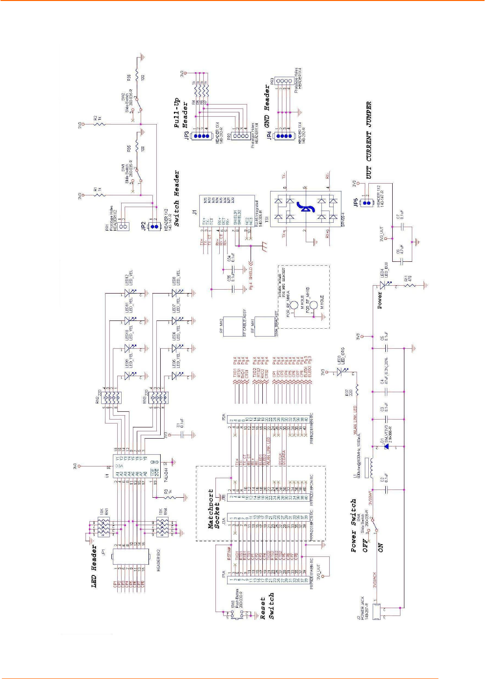
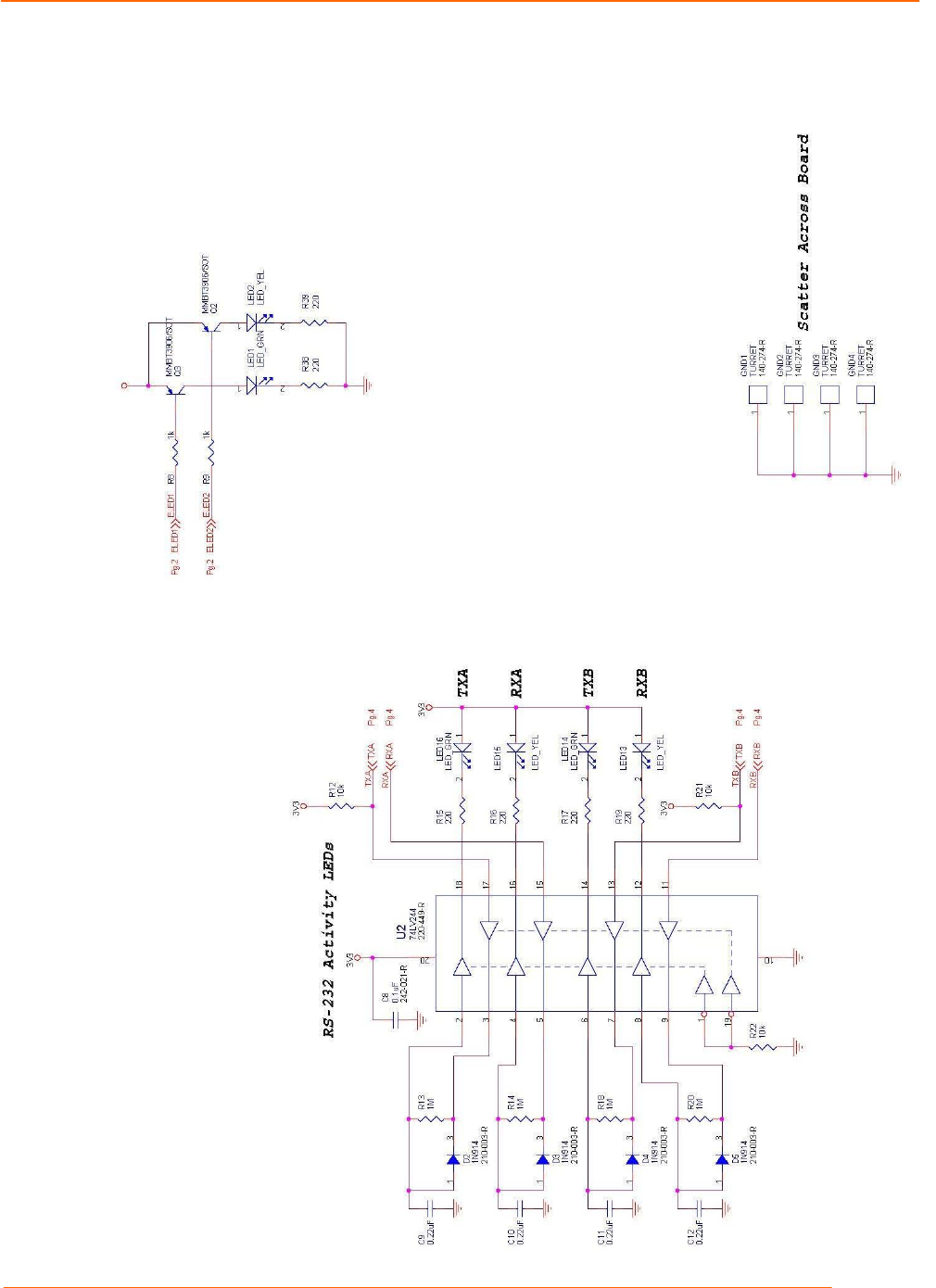
Figure 3-3. Schematic
3:Demonstration Kit
MatchPort b/g Pro Integration Guide 32
Figure 3-3. Schematic, continued
3:Demonstration Kit
MatchPort b/g Pro Integration Guide 33
Figure 3-3. Schematic, continued

MatchPort b/g Pro Integration Guide 34
A
A:
:
C
Co
om
mp
pl
li
ia
an
nc
ce
e
a
an
nd
d
W
Wa
ar
rr
ra
an
nt
ty
y
I
In
nf
fo
or
rm
ma
at
ti
io
on
n
Compliance Information
(According to ISO/IEC Guide 17050-1, 17050-2 and EN 45014)
Manufacturer’s Name & Address:
Lantronix 15353 Barranca Parkway, Irvine, CA 92618 USA
Product Name Model: MatchPort b/g Pro Embedded Device Server
Conforms to the following standards or other normative documents:
Safety:
UL 60950-1
CAN/CSA-C22.2 No. 60950-1-03
EN 60950-1:2006, Low Voltage Directive (73/23/EEC)
EMC & Radio:
For purposes of certification, the MatchPort b/g pro was tested as a modular device.
CFR Title 47 FCC Part 15, Subpart B and C, Class B
FCC Module Approval
FCC Identifier: R68MPBGPRO
Industry Canada ICES-003 Issue 4 (2004), Class B
Industry Canada RSS-Gen Issue 2 (2007)
Industry Canada RSS-210 Issue 7 (2007)
Industry Canada Module Approval IC: 3867A-MPBGPRO
EN 301 489-1 v1.6.1 (2006-07), EMC Directive (1999/5/EC)
EN 301 489-17 v.1.2.1 (2002-08), EMC Directive (1999/5/EC)
EN 300 328 v1.7.1 (2006-10), R&TTE Directive (1999/5/EC)
Australia / New Zealand AS/NZS CISPR 22 (2006), Class B
Australia / New Zealand AS/NZS 4771 (2000 + A1:2003)
EN55022: 2006
EN55024: 1998 + A1: 2001 + A2: 2003
EN61000-3-2: 2006
EN61000-3-3: 1995 + A1: 2001

A:Compliance and Warranty Information
MatchPort b/g Pro Integration Guide 35
Manufacturer’s Contact:
Director of Quality Assurance, Lantronix
15353 Barranca Parkway, Irvine, CA 92618 USA
Tel: 949-453-3990
Fax: 949-453-3995
Warranty
For details on the Lantronix warranty replacement policy, go to our web site at
www.lantronix.com/support/warranty