lantronix PW2050 PremierWave 2050 User Manual
lantronix PremierWave 2050
UserManual.wiki
>
lantronix
>
PW2050 User Manual
User Manual.pdf
Navigation menu
Upload a User Manual
Namespaces
Wiki Guide
HTML
PDF
Info
Views
User Manual
Discussion / Help
Navigation
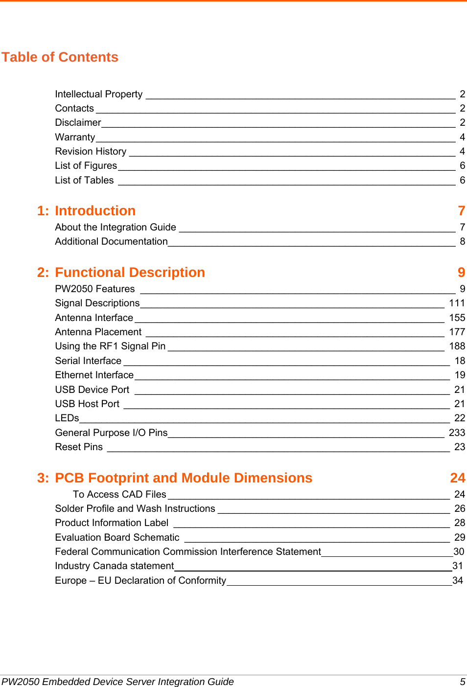
![PW2050 Embedded Device Server Integration Guide 10 ♦ 13 Configurable I/O pins ♦ Power supply filters ♦ Reset circuit ♦ Integrated wake up and shutdown for sleep and standby states ♦ Interface for connection to an external JTAG software debugger. ♦ Dedicated two wire serial port for debug The PW2050 Wi-Fi embedded device server requires +5-volt DC power and is designed to operate in an extended temperature range (see PW2050 data sheet for all technical specifications). Figure 錯誤! 使用 [常用] 索引標籤將 Heading 1 套用到您想要在此處顯示的文字。-1 PW2050 Dimensions and Views](https://usermanual.wiki/lantronix/PW2050/User-Guide-2842820-Page-10.png)
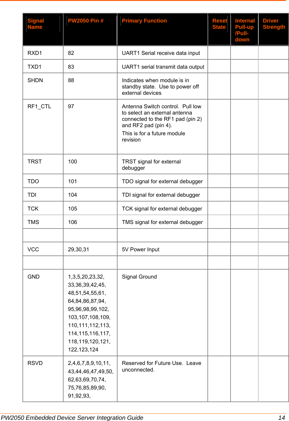
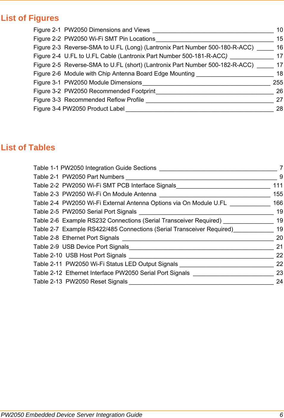
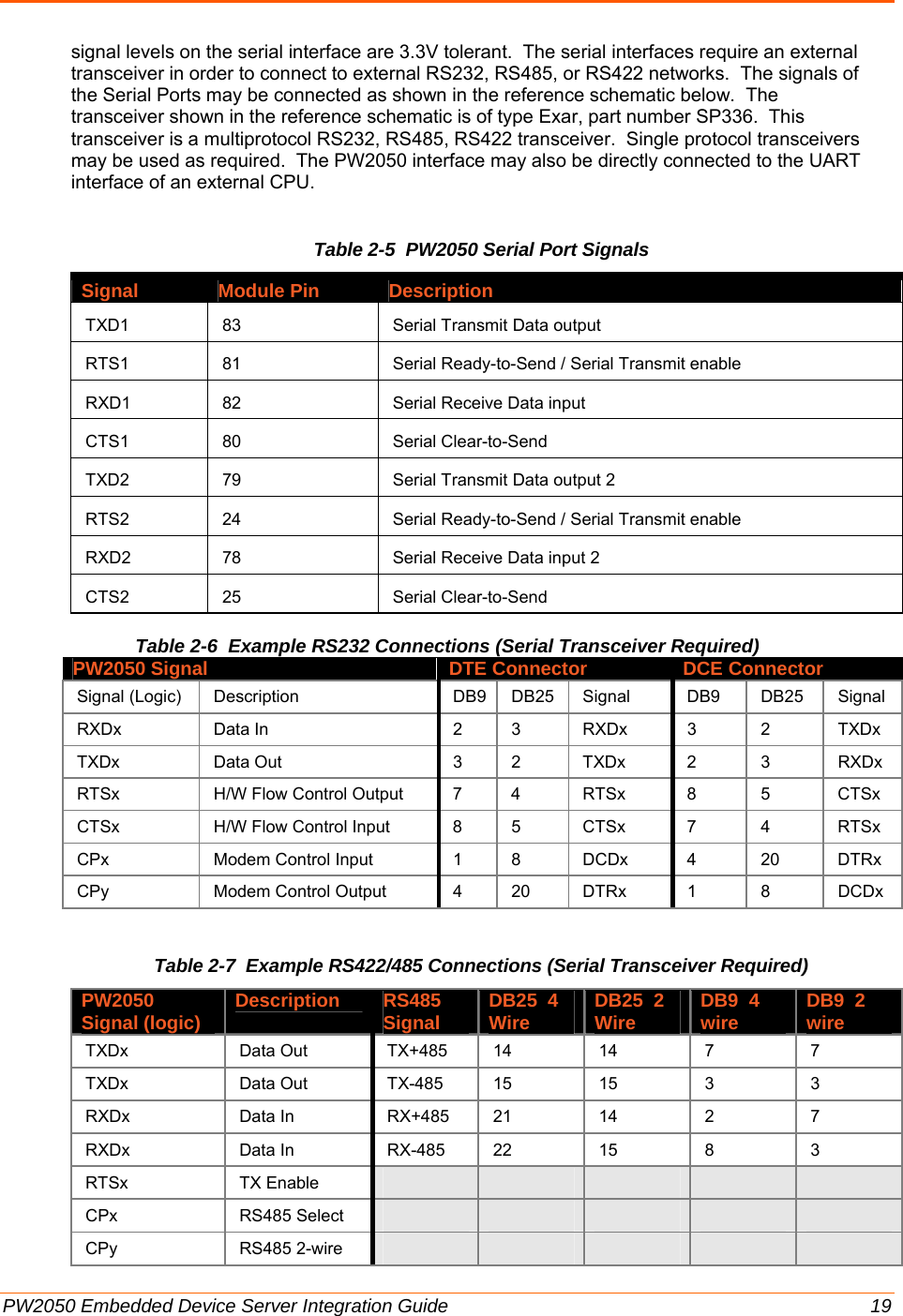
![PW2050 Embedded Device Server Integration Guide 15 Note1: The current module supports 10/100Mbps Ethernet. Additional pins have been called out for a future Gigabit Ethernet module. Note2: The logic IO pins are 3.3V tolerant. Note3: Pins 109 to 124 are the large ground pads under the module. These pads should be connected to ground. These pads also provide thermal relief for the module. It is recommended that multiple vias for each pad be used to connect the ground pads to the ground plane. Figure 錯誤! 使用 [常用] 索引標籤將 Heading 1 套用到您想要在此處顯示的文字。-2 PW2050 Wi-Fi SMT Pin Locations Note: Pins 109 to 124 are the large pads under the module. Pins 109 to 124 should be connected to GND. The pads in yellow are for future module revisions and should be left unconnected. Antenna Interface The PW2050 Wi-Fi module has been certified using the external antennas listed below. Per FCC guidelines, the PW2050 Wi-Fi certification remains valid if using an antenna of similar type to the antennas below. If using an antenna of similar type to one of the antennas below, but from a different manufacturer part number the antenna gain must be equal to or less than specified in the table. Refer to the PW2050 Wi-Fi SMT Embedded Device Server Data Sheet for full compliance instructions and information. Consult with your certification lab for more details. Table 2-3 PW2050 Wi-Fi On Module Antenna Antenna Type Peak Gain Typical Lantronix Part Number Vendor Vendor Part Number Approved Region Ceramic Antenna 2.17dBi, 2.4Ghz to 2.5Ghz 2.74dBi, 4.9Ghz to 5.8Ghz N/A N/A N/A FCC, IC, EU, AUS/NZS, JPN, China, 108 107 106 105 104 103 102 101 100 99 98 97 96 95 94 93 92 91 90 89 88 871 GND GND GND TMS TCK TDI GND GND TDO TRST GND GND RF1_CTL GND GND GND VCC2 VCC2 VCC2 VCC2 VCC2 SHDN GND GND 862RF1 RF3/GPS 853GND GND 844RF2 TXD1 835GND RXD1 826SDCK RTS1 817SDCMD CTS1 808SDIO0 TXD2 799SDIO1 RXD2 7810 SDIO2 RESET# 7711 SDIO3 VCC 7612 CP3/MISO VCC 7513 CP4/MOSI VCC 7414 CP7/SCK LED0/LNK 7315 CP8/CS LED1/ACT 7216 CP5/I2CDATA CP1 7117 CP6/I2CCLK SPARE1 7018 USB+ SPARE2 6919 USB‐CP2/INT 6820 GND SYS_LED 6721 USB2+ DEFAULT# 6622 USB2‐WAKE 6523 GND GND 6424 RTS2 ADC1 6325 CTS2 ADC2 6226 CP9 GND 6127 DBTX CP10/ TXD3 6028 DBRX CP11/RXD3 5929 VCC3 CP12/RTS3 5830 VCC3 CP13/CTS3 5731 VCC3 SPEEDLED 5632 GND GND 55GND ETX + ETX‐GND TXCT RXCT GND ERX+ ERX‐GND ETH3+ ETH3‐GND ETH4+ ETH4‐GND ECT3 ECT4 GND USB3+ USB3‐GND33 34 35 36 37 38 39 40 41 42 43 44 45 46 47 48 49 50 51 52 53 54GoldenGatePCBStripAntennaArea](https://usermanual.wiki/lantronix/PW2050/User-Guide-2842820-Page-15.png)
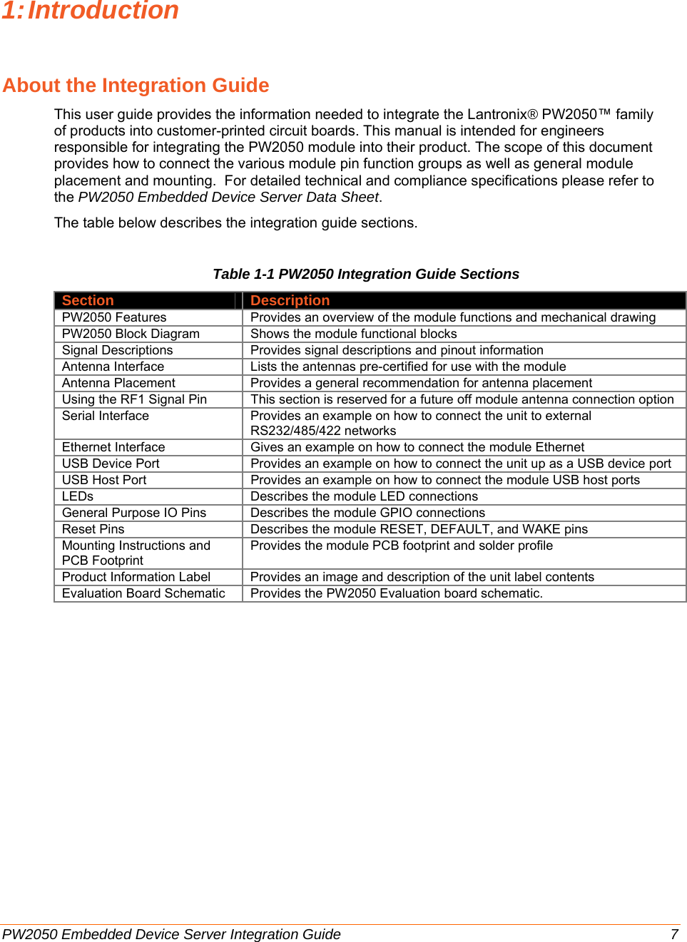
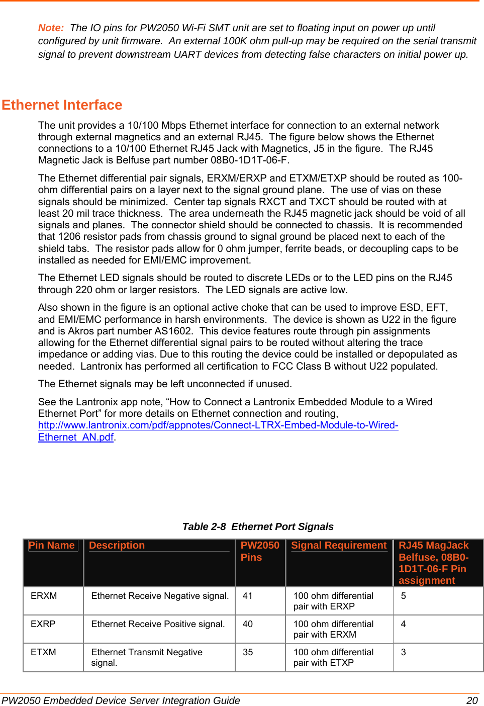
![PW2050 Embedded Device Server Integration Guide 16 Antenna Type Peak Gain Typical Lantronix Part Number Vendor Vendor Part Number Approved Region Mexico Table 2-4 PW2050 Wi-Fi External Antenna Options via On Module U.FL Antenna Type Peak Gain Typical Lantronix Part Number Vendor Vendor Part Number Approved Region PCB Strip Antenna with 50mm cable to U.FL connector With tape backing 2.5dBi, 2.39 Ghz to 2.49 Ghz 5dBi, 4.9Ghz to 5.9Ghz XPW100A003-01-B 50 piece bulk pack Ethertronics® 1001077 FCC, IC, EU, AUS/NZS, JPN, China, Mexico PCB Strip Antenna with 50mm cable to U.FL connector Without tape backing 2.5dBi, 2.39 Ghz to 2.49 Ghz 5dBi, 4.9Ghz to 5.9Ghz Ethertronics 1000668 FCC, IC, EU, AUS/NZS, JPN, China, Mexico Swivel type antenna, with RP-SMA(M) connector 2 dBi, 2.4 Ghz to 2.5 Ghz, 2 dBi, 5.15 Ghz to 5.85 Ghz 930-033-R-ACC 50 piece bulk pack Wanshih WSS002 FCC, IC, EU, AUS/NZS, JPN, China, Mexico Swivel type antenna, with RP-SMA(M) connector 3.8 dBi, 2.4Ghz to 2.5Ghz, 5.5 dBi, 4.9 Ghz to 5.8Ghz Taoglas GW.71.5153 (Not for EU use) FCC, IC, AUS/NZS, JPN, China, Mexico Note: The PCB strip antenna is available from Ethertronics with or without adhesive tape backing for mounting to a plastic case. The antennas Lantronix supplies include an adhesive backing. For the component without tape backing a non-conductive double sided adhesive tape can be used to fix the antenna in place. The Ethertronics part numbers listed above come with a 50mm U.FL cable attached to the PCB strip antenna. The 50mm cable length is the minimum allowed cable length for use with the PW2050 Wi-Fi embedded device server. For similar PCB strip antennas with longer cables consult with Ethertronics (www.ethertronics.com). Note: In order to use the on module U.FL connector signal RF1_CTL (pin 97) should be pulled high or left floating. Lantronix provides a U.FL to Reverse SMA antenna cable in with the evaluation board and sample kits for development work. These cables can be purchased from Lantronix for production or supplied by an RF cable manufacturer. External antennas can be purchased from an antenna vendor. Components for cable design should be selected for low loss over the entire 2.4Ghz to 5.9Ghz signal range. The cable target impedance should be 50 ohms. Figure 錯誤! 使用 [常用] 索引標籤將 Heading 1 套用到您想要在此處顯示的文字。-3 Reverse-SMA to U.FL (Long) (Lantronix Part Number 500-180-R-ACC)](https://usermanual.wiki/lantronix/PW2050/User-Guide-2842820-Page-16.png)
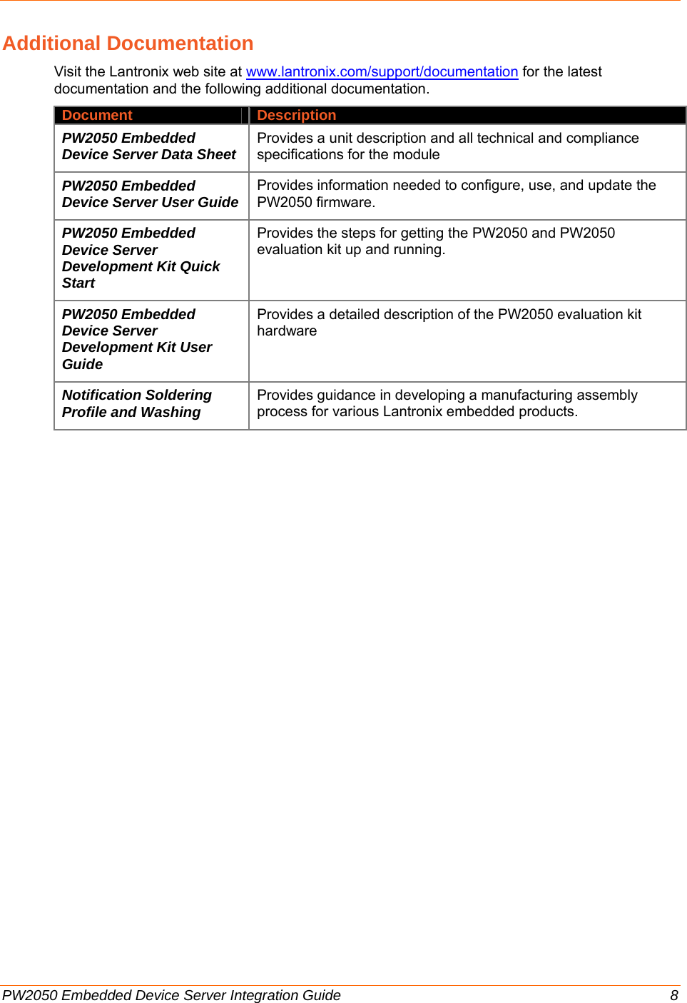
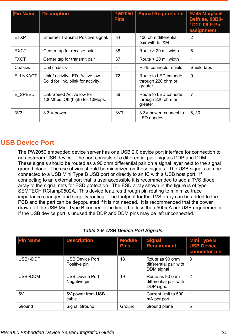
![PW2050 Embedded Device Server Integration Guide 17 Figure 錯誤! 使用 [常用] 索引標籤將 Heading 1 套用到您想要在此處顯示的文字。-4 U.FL to U.FL Cable (Lantronix Part Number 500-181-R-ACC) Figure 錯誤! 使用 [常用] 索引標籤將 Heading 1 套用到您想要在此處顯示的文字。-5 Reverse-SMA to U.FL (short) (Lantronix Part Number 500-182-R-ACC) Antenna Placement When designing the PW2050 Wi-Fi module to a mating board, it is important to consider the final installation of the unit and its location with respect to connecting access points. The antenna should be placed so that it has as clear as possible path to the connecting access point for maximum range. Avoid placing the antenna such that it is blocked by metal walls or ground planes of adjacent circuit boards. When using the on board chip antenna it is recommended to place the module such that the antenna region is along the edge of the board or extending outward from the edge of the board. The area under the chip antenna region should be voided of all signals and planes](https://usermanual.wiki/lantronix/PW2050/User-Guide-2842820-Page-17.png)
![PW2050 Embedded Device Server Integration Guide 18 See the figure images below showing recommended placement with the module chip antenna. Figure 錯誤! 使用 [常用] 索引標籤將 Heading 1 套用到您想要在此處顯示的文字。-6 Module with Chip Antenna Board Edge Mounting Note: The chip antenna region of the module shown in red above is at the top edge of the PCB. The area in red should be voided to optimize antenna performance. Using the RF1 Signal Pin Instructions TBD. Serial Interface The PW2050 Wi-Fi SMT embedded device servers has two external serial interfaces. The ExamplePCBPlacementEdgeofPCBVoidregioninred6mmx23mm](https://usermanual.wiki/lantronix/PW2050/User-Guide-2842820-Page-18.png)
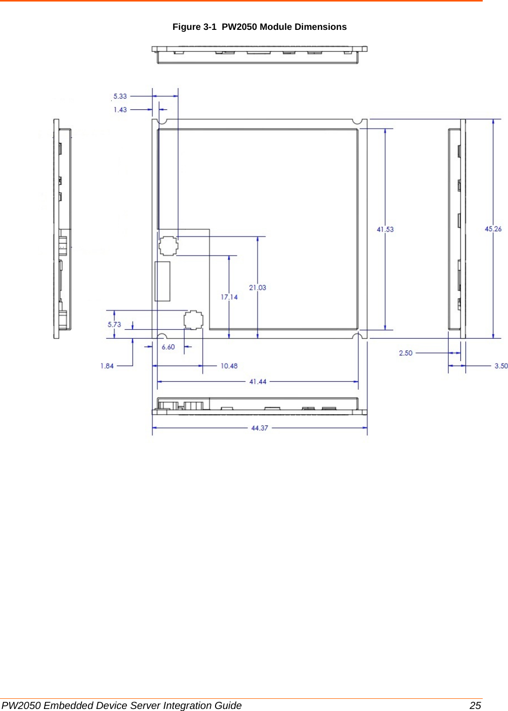
![PW2050 Embedded Device Server Integration Guide 26 Figure 錯誤! 使用 [常用] 索引標籤將 Heading 1 套用到您想要在此處顯示的文字。-2 PW2050 Recommended Footprint The internal ground pads are used for module signal ground and thermal relief. The outer layers should be flooded with ground and the ground pads should have many vias to the internal ground layers. Soldering coverage should be maximized and checked via x-ray for proper design. There is a trade-off between providing enough soldering for conductivity and applying too much, which allows the module to “float” on the pads creating reliability issues. Lantronix recommends 60% or more full contact solder coverage on each of the internal ground pads after reflow. In addition, Lantronix recommends that the solder wicks up at least 50% of the external LGA pads for proper signal connection. Solder Profile and Wash Instructions The reflow profile is dependent on many factors including flux selection, solder composition, and the capability of user's reflow equipment.](https://usermanual.wiki/lantronix/PW2050/User-Guide-2842820-Page-26.png)
![PW2050 Embedded Device Server Integration Guide 27 General guidelines are as follows: The solder composition typically sets the peak temperatures of the profile. Recommend lead free solder pastes SAC305: Type 4, water soluble or no clean are acceptable. Reflow equipment needed at least nine heater zones. Recommend forced air type reflow oven with nitrogen. It is recommended that the peak temperature at the solder joint be within 235°C ~ 245°C and the maximum component temperature should not exceed 245°C. It is recommended that time above 217°C for the solder joints is between 40-90 seconds, and with a minimum of 40 seconds. Excessive ramp/cooling rates >3°C per second should be avoided. To develop the reflow profile, it is recommended that the user place thermocouples at various locations on the assembly to confirm that all locations meet the profile requirements. The critical locations are the solder joints of SiP Module. When developing the reflow profile, it is recommended that the actual fully loaded assembly be used to make sure that the total thermal mass is accounted for. Figure 錯誤! 使用 [常用] 索引標籤將 Heading 1 套用到您想要在此處顯示的文字。-3 Recommended Reflow Profile (1) Solder paste alloy: SAC305(Sn96.5/Ag3.0/Cu0.5)(Lead free solder paste is recommended.) (2) A-B. Temperature (pre-heat): 150~200°C; soak time: 60~120 seconds (3) C. Peak temperature: 245°C (4) D. Time above 217°C: 40~90 seconds (5) Suggestion: Optimal cooling rate is 1°C per second from peak to 217°C (6) Nine heater zones at least for reflow equipment. (7) Nitrogen usage is recommended and the oxygen concentration is controlled less than 1500 parts per million. Note: Need to inspect solder joint by X-ray post reflow.](https://usermanual.wiki/lantronix/PW2050/User-Guide-2842820-Page-27.png)
![PW2050 Embedded Device Server Integration Guide 28 Product Information Label The product information label contains important information about your specific unit, such as its part number, revision, manufacturing date code, product model, country of origin, datamatrix barcode and MAC address. Figure 錯誤! 使用 [常用] 索引標籤將 Heading 1 套用到您想要在此處顯示的文字。-4 PW2050 Product Label](https://usermanual.wiki/lantronix/PW2050/User-Guide-2842820-Page-28.png)
![PW2050 Embedded Device Server Integration Guide 34 Broadband Radio Access Networks (BRAN); 5GHz high performance RLAN; Harmonized EN covering the essential requirements of article 3.2 of the R&TTE Directive (EMC) - EN 301 489-1 V1.9.2:2011 Electromagnetic compatibility and Radio spectrum Matters (ERM); ElectroMagnetic Compatibility (EMC) standard for radio equipment and services; Part 1: Common technical requirements - EN 301 489-3 V1.6.1:2013 Electromagnetic compatibility and Radio spectrum Matters (ERM); ElectroMagnetic Compatibility (EMC) standard for radio equipment and services; Part 3: Specific conditions for Short-Range Devices (SRD) operating on frequencies between 9 kHz and 246 GHz - EN 301 489-17 V2.2.1:2012 Electromagnetic compatibility and Radio spectrum Matters (ERM); ElectroMagnetic Compatibility (EMC) standard for radio equipment; Part 17: Specific conditions for Broadband Data Transmission Systems <Insert CE mark + notified body number + alert mark here> (除5G 未調和要放驚嘆號) Česky [Czech] [Jméno výrobce] tímto prohlašuje, že tento [typ zařízení] je ve shodě se základními požadavky a dalšími příslušnými ustanoveními směrnice 1999/5/ES. Dansk [Danish] Undertegnede [fabrikantens navn] erklærer herved, at følgende udstyr [udstyrets typebetegnelse] overholder de væsentlige krav og øvrige relevante krav i direktiv 1999/5/EF. Deutsch [German] Hiermit erklärt [Name des Herstellers], dass sich das Gerät [Gerätetyp] in Übereinstimmung mit den grundlegenden Anforderungen und den übrigen einschlägigen Bestimmungen der Richtlinie 1999/5/EG befindet. Eesti [Estonian] Käesolevaga kinnitab [tootja nimi = name of manufacturer] seadme [seadme tüüp = type of equipment] vastavust direktiivi 1999/5/EÜ põhinõuetele ja nimetatud direktiivist](https://usermanual.wiki/lantronix/PW2050/User-Guide-2842820-Page-34.png)
![PW2050 Embedded Device Server Integration Guide 35 tulenevatele teistele asjakohastele sätetele. English Hereby, [name of manufacturer], declares that this [type of equipment] is in compliance with the essential requirements and other relevant provisions of Directive 1999/5/EC. Español [Spanish] Por medio de la presente [nombre del fabricante] declara que el [clase de equipo] cumple con los requisitos esenciales y cualesquiera otras disposiciones aplicables o exigibles de la Directiva 1999/5/CE. Ελληνική [Greek] ΜΕ ΤΗΝ ΠΑΡΟΥΣΑ [name of manufacturer] ∆ΗΛΩΝΕΙ ΟΤΙ [type of equipment] ΣΥΜΜΟΡΦΩΝΕΤΑΙ ΠΡΟΣ ΤΙΣ ΟΥΣΙΩ∆ΕΙΣ ΑΠΑΙΤΗΣΕΙΣ ΚΑΙ ΤΙΣ ΛΟΙΠΕΣ ΣΧΕΤΙΚΕΣ ∆ΙΑΤΑΞΕΙΣ ΤΗΣ Ο∆ΗΓΙΑΣ 1999/5/ΕΚ. Français [French] Par la présente [nom du fabricant] déclare que l'appareil [type d'appareil] est conforme aux exigences essentielles et aux autres dispositions pertinentes de la directive 1999/5/CE. Italiano [Italian] Con la presente [nome del costruttore] dichiara che questo [tipo di apparecchio] è conforme ai requisiti essenziali ed alle altre disposizioni pertinenti stabilite dalla direttiva 1999/5/CE. Latviski [Latvian] Ar šo [name of manufacturer / izgatavotāja nosaukums] deklarē, ka [type of equipment / iekārtas tips] atbilst Direktīvas 1999/5/EK būtiskajām prasībām un citiem ar to saistītajiem noteikumiem. Lietuvių [Lithuanian] Šiuo [manufacturer name] deklaruoja, kad šis [equipment type] atitinka esminius reikalavimus ir kitas 1999/5/EB Direktyvos nuostatas. Nederlands [Dutch] Hierbij verklaart [naam van de fabrikant] dat het toestel [type van toestel] in overeenstemming is met de essentiële eisen en de andere relevante bepalingen van richtlijn 1999/5/EG. Malti [Maltese] Hawnhekk, [isem tal-manifattur], jiddikjara li dan [il-mudel tal-prodott] jikkonforma mal-ħtiġijiet essenzjali u ma provvedimenti oħrajn relevanti li hemm fid-Dirrettiva 1999/5/EC. Magyar [Hungarian] Alulírott, [gyártó neve] nyilatkozom, hogy a [... típus] megfelel a vonatkozó alapvetõ követelményeknek és az 1999/5/EC irányelv egyéb elõírásainak. Polski [Polish] Niniejszym [nazwa producenta] oświadcza, że [nazwa wyrobu] jest zgodny z zasadniczymi wymogami oraz pozostałymi stosownymi postanowieniami Dyrektywy 1999/5/EC. Português [Portuguese] [Nome do fabricante] declara que este [tipo de equipamento] está conforme com os requisitos essenciais e outras disposições da Directiva 1999/5/CE. Slovensko [Ime proizvajalca] izjavlja, da je ta [tip opreme] v skladu z bistvenimi zahtevami in ostalimi](https://usermanual.wiki/lantronix/PW2050/User-Guide-2842820-Page-35.png)
![PW2050 Embedded Device Server Integration Guide 36 [Slovenian] relevantnimi določili direktive 1999/5/ES. Slovensky [Slovak] [Meno výrobcu] týmto vyhlasuje, že [typ zariadenia] spĺňa základné požiadavky a všetky príslušné ustanovenia Smernice 1999/5/ES. Suomi [Finnish] [Valmistaja = manufacturer] vakuuttaa täten että [type of equipment = laitteen tyyppimerkintä] tyyppinen laite on direktiivin 1999/5/EY oleellisten vaatimusten ja sitä koskevien direktiivin muiden ehtojen mukainen. Svenska [Swedish] Härmed intygar [företag] att denna [utrustningstyp] står I överensstämmelse med de väsentliga egenskapskrav och övriga relevanta bestämmelser som framgår av direktiv 1999/5/EG. 查詢 NB no. http://ec.europa.eu/enterprise/newapproach/nando/index.cfm?fuseaction=notifiedbody.main](https://usermanual.wiki/lantronix/PW2050/User-Guide-2842820-Page-36.png)