lantronix PW2050 PremierWave 2050 User Manual
lantronix PremierWave 2050
User Manual.pdf
Part Number 900-731-R
Revision A.2 October 2015
PW2050
Embedded Device Server
Integration Guide

PW2050 Embedded Device Server Integration Guide 2
Intellectual Property
© 2015 Lantronix, Inc. All rights reserved. No part of the contents of this publication may be
transmitted or reproduced in any form or by any means without the written permission of
Lantronix.
Lantronix is a registered trademark of Lantronix, Inc. in the United States and other countries.
Patented: patents.lantronix.com; Additional patents pending.
Windows is a registered trademark of Microsoft Corporation. Wi-Fi is a registered trademark of
Wi-Fi Alliance Corporation. Ethertronics is a trademark of Ethertronics, Inc. Wanshih is a
trademark of Wanshih Electronic Co., Ltd. Exar is a trademark of Exar Corporation.
SEMTECH is a trademark of Semtech Corporation. All other trademarks and trade names are
the property of their respective holders.
Contacts
Lantronix, Inc.
7535 Irvine Center Drive, Suite 100
Irvine, CA 92618, USA
Toll Free: 800-526-8766
Phone: 949-453-3990
Fax: 949-453-3995
Technical Support
Online: www.lantronix.com/support
Sales Offices
For a current list of our domestic and international sales offices, go to the Lantronix web site at
www.lantronix.com/about/contact
Disclaimer
All information contained herein is provided “AS IS.” Lantronix undertakes no obligation to
update the information in this publication. Lantronix does not make, and specifically disclaims,
all warranties of any kind (express, implied or otherwise) regarding title, non-infringement,
fitness, quality, accuracy, completeness, usefulness, suitability or performance of the
information provided herein. Lantronix shall have no liability whatsoever to any user for any
damages, losses and causes of action (whether in contract or in tort or otherwise) in
connection with the user’s access or usage of any of the information or content contained
herein. The information and specifications contained in this document are subject to change
without notice.
This equipment has to be tested and found to comply with the limits for a Class B digital device,
pursuant to Part 15 of the FCC Rules. These limits are designed to provide reasonable
protection against harmful interference in a residential installation. This equipment generates,
uses, and can radiate radio frequency energy and, if not installed and used in accordance with
the instructions, may cause harmful interference to radio communications. However, there is
no guarantee that interference will not occur in a particular installation.

PW2050 Embedded Device Server Integration Guide 3
If this equipment does cause harmful interference to radio or television reception, which can be
determined by turning the equipment off and on, the user is encouraged to try to correct the
interference by one of the following measures:
1. Reorient or relocate the receiving antenna.
2. Increase the separation between the equipment and receiver.
3. Connect the equipment into an outlet on a circuit different from that to which the receiver
is connected.
4. Consult the dealer or an experienced radio/TV technician for help.
This device complies with Part 15 of the FCC Rules. Operation is subject to the following two
conditions: (1) This device may not cause harmful interference, and (2) this device must accept
any interference received, including interference that may cause undesired operation.
This device is intended only for OEM Integrators. The OEM integrator should be aware of the
following important considerations.
Labeling of the End Product
The label on the end product incorporating the PW2050 module must clearly state that it
contains an FCC-approved RF module. Canada and Japan also require a similar statement.
For example, “This product contains RF transmitter ID # (put FCC, IC, and/or Japan module
grant numbers here).” The label must include the ID numbers for the regions where the end
product is installed. The grant numbers are below.
♦
PW2050 FCC ID number: R68PW2050
♦
PW2050 IC ID number: 3867A-PW2050
♦
PW2050 Japan ID numbers: TBD
RSS-GEN Sections 7.1.4 and 7.1.5 Statement for Devices with Detachable Antennas
This device has been designed to operate with the antennas listed in the Certificate, and
having a maximum gain of 5.5 dBi. Antennas not included in this list or having a gain greater
than 5.5 dBi are strictly prohibited for use with this device, unless system level approval is
gained. The required antenna impedance is 50 ohms.
To reduce potential radio interference to other users, the antenna type and its gain should be
so chosen that the equivalent isotropically radiated power (EIRP) is not more than that
required for successful communication.
Integration Notes
This module is to be authorized under limited module approval specified to mobile host
equipment. So, the antenna must be installed such that 20cm is maintained between the
antenna and users.
The transmitter module may not be co-located with any other transmitter or antenna.
As long as the two conditions above are met, further transmitter testing will not be required.
However, the OEM integrator is still responsible for testing their end product for any additional
compliance requirements required with this module installed (for example, digital device
emission, PC peripheral requirements, etc.)

PW2050 Embedded Device Server Integration Guide 4
In the event that these conditions cannot be met (for example certain laptop configurations,
general purpose PCMCIA or similar cards, or co-location with another transmitter) and
obtaining a separate FCC authorization will be required, then the FCC authorization is no
longer considered valid and the FCC ID cannot be used on the final product (including the
transmitter).
Changes or modifications to this device not explicitly approved by Lantronix will void the user's
authority to operate this device.
Note: With the purchase of any PW2050 family product, the OEM agrees to an OEM
firmware license agreement that grants the OEM a non-exclusive, royalty-free firmware
license to use and distribute the binary firmware image provided, only to the extent
necessary to use the PW2050 hardware. For further details, please see the PW2050
OEM firmware license agreement.
Note: Please refer to the PW2050 Data Sheet for the full compliance specification and
requirements.
Warranty
For details on the Lantronix warranty policy, please go to our Web site at
www.lantronix.com/support/warranty.
Revision History
Date Rev. Comments
October 2015 A.2 Preliminary draft.
For the latest revision of this product document, please check our online documentation at
www.lantronix.com/support/documentation.

PW2050 Embedded Device Server Integration Guide 5
Table of Contents
Intellectual Property ________________________________________________________ 2
Contacts _________________________________________________________________ 2
Disclaimer _______ ___________ ______________ ___________ ___________ __________ 2
Warranty _________________________________________________________________ 4
Revision History ___________________________________________________________ 4
List of Figures _____________________________________________________________ 6
List of Tables _____________________________________________________________ 6
1:Introduction 7
About the Integration Guide __________________________________________________ 7
Additional Documentation____________________________________________________ 8
2:Functional Description 9
PW2050 Features _________________________________________________________ 9
Signal Descriptions _______________________________________________________ 111
Antenna Interface ________________________________________________________ 155
Antenna Placement ______________________________________________________ 177
Using the RF1 Signal Pin __________________________________________________ 188
Serial Interface ___________________________________________________________ 18
Ethernet Interface _________________________________________________________ 19
USB Device Port _________________________________________________________ 21
USB Host Port ___________________________________________________________ 21
LEDs ___________________________________________________________________ 22
General Purpose I/O Pins__________________________________________________ 233
Reset Pins ______________________________________________________________ 23
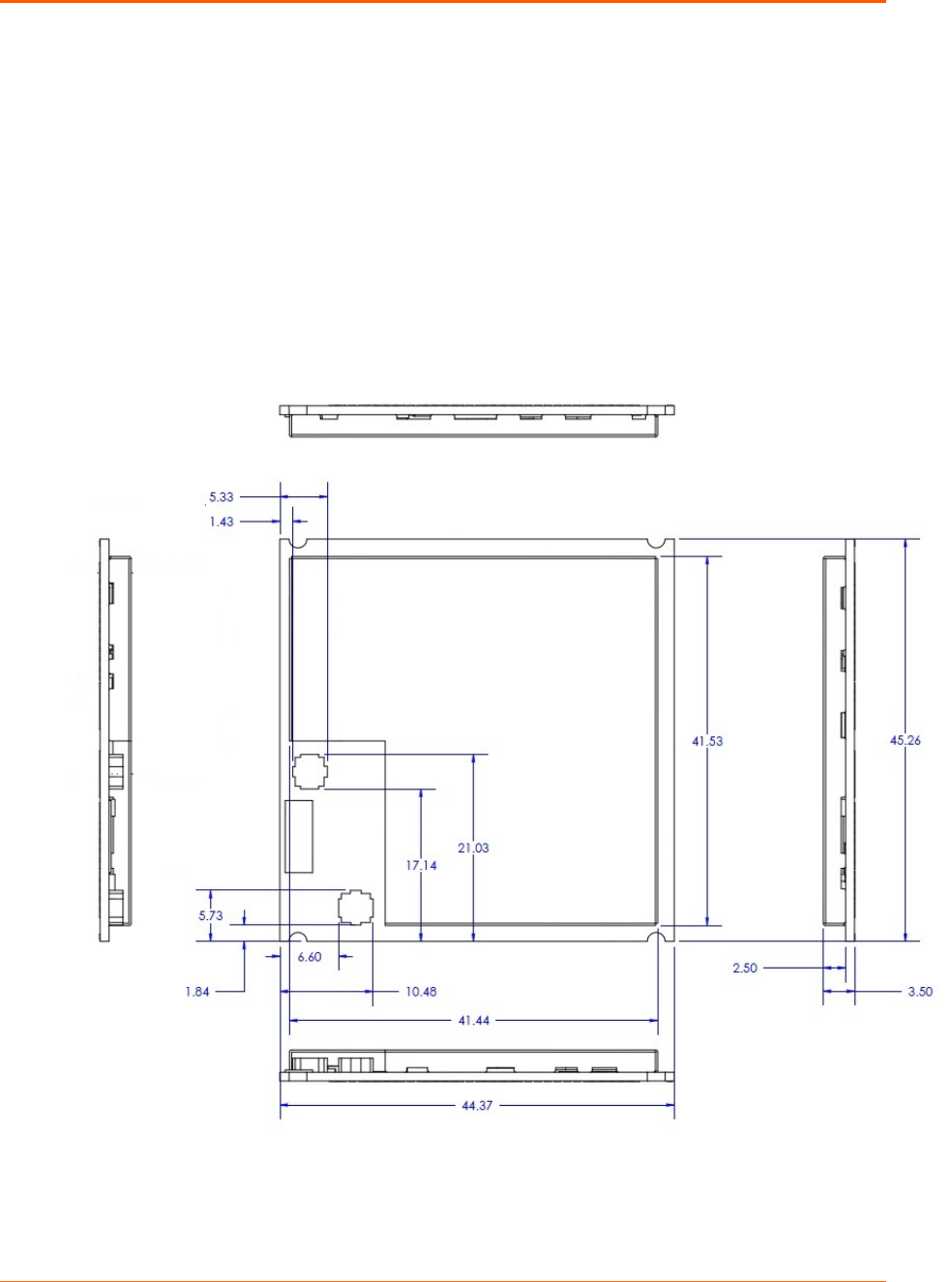
3:PCB Footprint and Module Dimensions 24
To Access CAD Files ___________________________________________________ 24
Solder Profile and Wash Instructions __________________________________________ 26
Product Information Label __________________________________________________ 28
Evaluation Board Schematic ________________________________________________ 29
Federal Communication Commission Interference Statement 30
Industry Canada statement 31
Europe – EU Declaration of Conformity 34

PW2050 Embedded Device Server Integration Guide 6
List of Figures
Figure 2-1 PW2050 Dimensions and Views ____________________________________ 10
Figure 2-2 PW2050 Wi-Fi SMT Pin Locations ___________________________________ 15
Figure 2-3 Reverse-SMA to U.FL (Long) (Lantronix Part Number 500-180-R-ACC) _____ 16
Figure 2-4 U.FL to U.FL Cable (Lantronix Part Number 500-181-R-ACC) _____________ 17
Figure 2-5 Reverse-SMA to U.FL (short) (Lantronix Part Number 500-182-R-ACC) _____ 17
Figure 2-6 Module with Chip Antenna Board Edge Mounting _______________________ 18
Figure 3-1 PW2050 Module Dimensions ______________________________________ 255
Figure 3-2 PW2050 Recommended Footprint ___________________________________ 26
Figure 3-3 Recommended Reflow Profile ______________________________________ 27
Figure 3-4 PW2050 Product Label ____________________________________________ 28
List of Tables
Table 1-1 PW2050 Integration Guide Sections ___________________________________ 7
Table 2-1 PW2050 Part Numbers _____________________________________________ 9
Table 2-2 PW2050 Wi-Fi SMT PCB Interface Signals____________________________ 111
Table 2-3 PW2050 Wi-Fi On Module Antenna _________________________________ 155
Table 2-4 PW2050 Wi-Fi External Antenna Options via On Module U.FL ____________ 166
Table 2-5 PW2050 Serial Port Signals ________________________________________ 19
Table 2-6 Example RS232 Connections (Serial Transceiver Required) _______________ 19
Table 2-7 Example RS422/485 Connections (Serial Transceiver Required) ____________ 19
Table 2-8 Ethernet Port Signals _____________________________________________ 20
Table 2-9 USB Device Port Signals ___________________________________________ 21
Table 2-10 USB Host Port Signals ___________________________________________ 22
Table 2-11 PW2050 Wi-Fi Status LED Output Signals ____________________________ 22
Table 2-12 Ethernet Interface PW2050 Serial Port Signals ________________________ 23
Table 2-13 PW2050 Reset Signals ___________________________________________ 24

PW2050 Embedded Device Server Integration Guide 7
1: Introduction
About the Integration Guide
This user guide provides the information needed to integrate the Lantronix® PW2050™ family
of products into customer-printed circuit boards. This manual is intended for engineers
responsible for integrating the PW2050 module into their product. The scope of this document
provides how to connect the various module pin function groups as well as general module
placement and mounting. For detailed technical and compliance specifications please refer to
the PW2050 Embedded Device Server Data Sheet.
The table below describes the integration guide sections.
Table 1-1 PW2050 Integration Guide Sections
Section Description
PW2050 Features Provides an overview of the module functions and mechanical drawing
PW2050 Block Diagram Shows the module functional blocks
Signal Descriptions Provides signal descriptions and pinout information
Antenna Interface Lists the antennas pre-certified for use with the module
Antenna Placement Provides a general recommendation for antenna placement
Using the RF1 Signal Pin This section is reserved for a future off module antenna connection option
Serial Interface Provides an example on how to connect the unit to external
RS232/485/422 networks
Ethernet Interface Gives an example on how to connect the module Ethernet
USB Device Port Provides an example on how to connect the unit up as a USB device port
USB Host Port Provides an example on how to connect the module USB host ports
LEDs Describes the module LED connections
General Purpose IO Pins Describes the module GPIO connections
Reset Pins Describes the module RESET, DEFAULT, and WAKE pins
Mounting Instructions and
PCB Footprint
Provides the module PCB footprint and solder profile
Product Information Label Provides an image and description of the unit label contents
Evaluation Board Schematic Provides the PW2050 Evaluation board schematic.

PW2050 Embedded Device Server Integration Guide 8
Additional Documentation
Visit the Lantronix web site at www.lantronix.com/support/documentation for the latest
documentation and the following additional documentation.
Document Description
PW2050 Embedded
Device Server Data Sheet Provides a unit description and all technical and compliance
specifications for the module
PW2050 Embedded
Device Server User Guide Provides information needed to configure, use, and update the
PW2050 firmware.
PW2050 Embedded
Device Server
Development Kit Quick
Start
Provides the steps for getting the PW2050 and PW2050
evaluation kit up and running.
PW2050 Embedded
Device Server
Development Kit User
Guide
Provides a detailed description of the PW2050 evaluation kit
hardware
Notification Soldering
Profile and Washing Provides guidance in developing a manufacturing assembly
process for various Lantronix embedded products.

PW2050 Embedded Device Server Integration Guide 9
2: Functional Description
Designed for quick integration with minimal engineering effort, the chip-sized PW2050
embedded device server provides simplicity and flexibility making it the easiest and fastest
networking-enabling module on the market.
PW2050 device servers are extremely compact networking solution that enables Ethernet or
Wireless connectivity on virtually any device with a serial interface. The included industry-
proven Lantronix device server application and full IP stack allow seamless remote access to
device data simplifying design integration while providing robust connectivity.
The PW2050 embedded device servers can be utilized in designs typically intended for chip
solutions. A key difference with the PW2050 module is that there is virtually no need to write a
single line of code, translating to a much lower development cost and faster time-to-market.
Table 2-1 PW2050 Part Numbers
Part Number Description
TBD PW2050 with on module U.FL— IEEE 802.11 ac/b/g/n Device Server Module, Extended
Temp, Bulk, RoHS
TBD PW2050 with on module chip antenna— IEEE 802.11 ac/b/g/n Device Server Module,
Extended Temp, Bulk, RoHS
TBD PW2050 — IEEE 802.11 ac/b/g/n Device Server Development Kit w/ on Module U.FL
and RF Cable to External Antenna, RoHS
TBD PW2050— IEEE 802.11 ac/b/g/n Device Server Development Kit w/ on Module Chip
Antenna, RoHS
PW2050 Features
The PW2050 device server is built around a 400Mhz ARM9 processor with 32MB of DDR2
DRAM and 128MB of embedded Flash memory. Network connections are provided by a dual
band 802.11 ac/b/g/n WLAN radio and 10/100Mbps Ethernet MAC and PHY.
The PW2050 embedded device server also supports the following:
♦
400Mhz ARM9 CPU
♦
32MB DDR2 DRAM
♦
128MB NAND Flash
♦
802.11AC/BGN wireless with option for on module antenna or on module U.FL
♦
On module 10/100Mbps Ethernet MAC/PHY. External magnetic and RJ45 required.
♦
One USB2.0 High Speed Host/Device interface.
♦
One USB2.0 High Speed Host only port
♦
One USB2.0 Full Speed Host only port
♦
Two 3.3-volt serial interface
PW2050 Embedded Device Server Integration Guide 10
♦
13 Configurable I/O pins
♦
Power supply filters
♦
Reset circuit
♦
Integrated wake up and shutdown for sleep and standby states
♦
Interface for connection to an external JTAG software debugger.
♦
Dedicated two wire serial port for debug
The PW2050 Wi-Fi embedded device server requires +5-volt DC power and is designed to
operate in an extended temperature range (see PW2050 data sheet for all technical
specifications).
Figure 錯誤! 使用 [常用] 索引標籤將 Heading 1 套用到您想要在此處顯示的文字。-1 PW2050 Dimensions
and Views

PW2050 Embedded Device Server Integration Guide 11
Signal Descriptions
The PW2050 embedded device server has a serial interface compatible with data rates up to
921,600 bps (in high-performance mode). All of the logic IO pins are 3.3V tolerant. The serial
signals usually connect to an internal device, such as a UART. For applications requiring an
external cable running with RS-232 or RS422/485 voltage levels, the PW2050 must interface
to a serial transceiver chip.
An on module 10/100Mbps Ethernet MAC and PHY are included on the module. For
connection to an external Ethernet network external magnetics and an RJ45 are required.
The module has options for an on-module chip antenna and an external antenna via an on-
module U.FL connection.
Table 2-2 PW2050 Wi-Fi SMT PCB Interface Signals
Signal
Name PW2050 Pin # Primary Function Reset
State Internal
Pull-up
/Pull-
down
Driver
Strength
RF1 2 RF signal to PCB trace when
RF1_CTL is asserted low (Future
module versions only)
RF2 4 RF signal to PCB trace when
RF1_CTL is asserted low (Future
module versions only)
CP3/MISO 12 Configurable GPIO / SPI Master
serial data input, SPI Slave serial
data output
CP4/MOSI 13 Configurable GPIO / SPI Master
serial data output, SPI Slave
serial data input
CP7/SCK 14 Configurable GPIO / SPI clock
CP8/CS 15 Configurable GPIO, multiplexed
with SPI interface Chip Select
CP5 16 Configurable GPIO /
I2C Data 10K PU
CP6 17 Configurable GPIO / I2C Clock 10K PU
USB1+/DDP 18 USB (Positive)
USB High Speed Host/Device
Port
USB1-/DDM 19 USB (Negative)
USB High Speed Host/Device
Port
USB2+ 21 USB (Positive)
USB High Speed Host Port

PW2050 Embedded Device Server Integration Guide 12
Signal
Name PW2050 Pin # Primary Function Reset
State Internal
Pull-up
/Pull-
down
Driver
Strength
USB2- 22 USB (Negative)
USB High Speed Host Port
RTS2 24 UART2 serial ready to send
output
CTS2 25 UART2 clear to send input
CP9 26 Configurable GPIO
DBTX 27 Debug UART serial transmit data
output
DBRX 28 Debug UART serial receive data
input
10K PU
ETXP
(ETH1+)
34 Ethernet TX (positive)
Future Gbit pair 1 (pos)
ETXM
(ETH1-)
35 Ethernet TX (negative)
Future Gbit pair 1 (net)
TXCT
(ECT1)_
37 Center Tap connection for
Ethernet TX pair
RXCT
(ECT2)
38 Center Tap connection for
Ethernet RX pair
ERXP
(ETH2+)
40 Ethernet RX (positive)
Future Gbit pair 2 (pos)
ERXM
(ETH2-)
41 Ethernet RX (negative)
Future Gbit pair 2 (neg)
ETH3+ 43 Reserved for future Gbit Ethernet
pair 3 (positive)
ETH3- 44 Reserved for future Gbit Ethernet
pair 3 (negative)
ETH4+ 46 Reserved for future Gbit Ethernet
pair 4 (positive)
ETH4- 47 Reserved for future Gbit Ethernet
pair 4 (negative)
ECT3 49 Reserved for future Gbit center
tap 3 connection
ECT4 50 Reserved for future Gbit center
tap 4 connection

PW2050 Embedded Device Server Integration Guide 13
Signal
Name PW2050 Pin # Primary Function Reset
State Internal
Pull-up
/Pull-
down
Driver
Strength
USB3+ 52 USB (Positive)
USB Full Speed Host Port
USB3- 53 USB (Negative)
USB Full Speed Host Port
SPEED_LED 56 Ethernet Speed LED, Active low
for 100Mbps
CP13 57 Configurable GPIO
CP12 58 Configurable GPIO
CP11 59 Configurable GPIO
CP10 60 Configurable GPIO
WAKE 65 CPU Wake up input. Module
wakes from low power state on a
rising edge
100K
PU
DEFAULT# 66 Unit reset to default, active low.
Drive low for xx seconds to reset
unit to default settings.
SYS_LED 67 System Status LED, Active High
CP2/INT 68 Configurable GPIO / SPI interrupt
External Interrupt input
CP1 71 Configurable GPIO
LINK_ACT 72 Ethernet Link/Activity LED
Active low for link.
Toggle for activity.
WLAN LED 73 LED function for WLAN Link
indication, Active Low
RESET# 77 Unit hardware reset, active low.
Drive low to reboot unit 35K PU
RXD2 78 UART2 serial receive data input
TXD2 79 UART2 serial transmit data output
CTS1 80 UART1 clear to send input
RTS1 81 UART1 serial ready to send
output

PW2050 Embedded Device Server Integration Guide 14
Signal
Name PW2050 Pin # Primary Function Reset
State Internal
Pull-up
/Pull-
down
Driver
Strength
RXD1 82 UART1 Serial receive data input
TXD1 83 UART1 serial transmit data output
SHDN 88 Indicates when module is in
standby state. Use to power off
external devices
RF1_CTL 97 Antenna Switch control. Pull low
to select an external antenna
connected to the RF1 pad (pin 2)
and RF2 pad (pin 4).
This is for a future module
revision
TRST 100 TRST signal for external
debugger
TDO 101 TDO signal for external debugger
TDI 104 TDI signal for external debugger
TCK 105 TCK signal for external debugger
TMS 106 TMS signal for external debugger
VCC 29,30,31 5V Power Input
GND 1,3,5,20,23,32,
33,36,39,42,45,
48,51,54,55,61,
64,84,86,87,94,
95,96,98,99,102,
103,107,108,109,
110,111,112,113,
114,115,116,117,
118,119,120,121,
122,123,124
Signal Ground
RSVD 2,4,6,7,8,9,10,11,
43,44,46,47,49,50,
62,63,69,70,74,
75,76,85,89,90,
91,92,93,
Reserved for Future Use. Leave
unconnected.
PW2050 Embedded Device Server Integration Guide 15
Note1: The current module supports 10/100Mbps Ethernet. Additional pins have been called out for a future Gigabit
Ethernet module.
Note2: The logic IO pins are 3.3V tolerant.
Note3: Pins 109 to 124 are the large ground pads under the module. These pads should be connected to ground.
These pads also provide thermal relief for the module. It is recommended that multiple vias for each pad be used to
connect the ground pads to the ground plane.
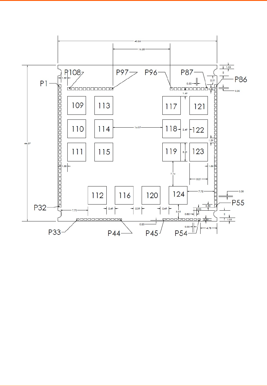
Figure 錯誤! 使用 [常用] 索引標籤將 Heading 1 套用到您想要在此處顯示的文字。-2 PW2050 Wi-Fi SMT
Pin Locations
Note: Pins 109 to 124 are the large pads under the module. Pins 109 to 124 should be
connected to GND. The pads in yellow are for future module revisions and should be left
unconnected.
Antenna Interface
The PW2050 Wi-Fi module has been certified using the external antennas listed below. Per
FCC guidelines, the PW2050 Wi-Fi certification remains valid if using an antenna of similar
type to the antennas below. If using an antenna of similar type to one of the antennas below,
but from a different manufacturer part number the antenna gain must be equal to or less than
specified in the table. Refer to the PW2050 Wi-Fi SMT Embedded Device Server Data Sheet
for full compliance instructions and information. Consult with your certification lab for more
details.
Table 2-3 PW2050 Wi-Fi On Module Antenna
Antenna Type Peak Gain Typical Lantronix
Part
Number
Vendor Vendor
Part
Number
Approved
Region
Ceramic Antenna 2.17dBi, 2.4Ghz to 2.5Ghz
2.74dBi, 4.9Ghz to 5.8Ghz
N/A N/A N/A FCC, IC,
EU,
AUS/NZS,
JPN, China,
108 107 106 105 104 103 102 101 100 99 98 97 96 95 94 93 92 91 90 89 88 87
1 GND GND GND TMS TCK TDI GND GND TDO TRST GND GND RF1_CTL GND GND GND VCC2 VCC2 VCC2 VCC2 VCC2 SHDN GND GND 86
2RF1 RF3/GPS 85
3GND GND 84
4RF2 TXD1 83
5GND RXD1 82
6SDCK RTS1 81
7SDCMD CTS1 80
8SDIO0 TXD2 79
9SDIO1 RXD2 78
10 SDIO2 RESET# 77
11 SDIO3 VCC 76
12 CP3/MISO VCC 75
13 CP4/MOSI VCC 74
14 CP7/SCK LED0/LNK 73
15 CP8/CS LED1/ACT 72
16 CP5/I2CDATA CP1 71
17 CP6/I2CCLK SPARE1 70
18 USB+ SPARE2 69
19 USB‐CP2/INT 68
20 GND SYS_LED 67
21 USB2+ DEFAULT# 66
22 USB2‐WAKE 65
23 GND GND 64
24 RTS2 ADC1 63
25 CTS2 ADC2 62
26 CP9 GND 61
27 DBTX CP10/ TXD3 60
28 DBRX CP11/RXD3 59
29 VCC3 CP12/RTS3 58
30 VCC3 CP13/CTS3 57
31 VCC3 SPEEDLED 56
32 GND GND 55
GND ETX + ETX‐GND TXCT RXCT GND ERX+ ERX‐GND ETH3+ ETH3‐GND ETH4+ ETH4‐GND ECT3 ECT4 GND USB3+ USB3‐GND
33 34 35 36 37 38 39 40 41 42 43 44 45 46 47 48 49 50 51 52 53 54
GoldenGate
PCBStripAntennaArea
PW2050 Embedded Device Server Integration Guide 16
Antenna Type Peak Gain Typical Lantronix
Part
Number
Vendor Vendor
Part
Number
Approved
Region
Mexico
Table 2-4 PW2050 Wi-Fi External Antenna Options via On Module U.FL
Antenna Type Peak Gain Typical Lantronix
Part
Number
Vendor Vendor
Part
Number
Approved
Region
PCB Strip Antenna with
50mm cable to U.FL
connector
With tape backing
2.5dBi, 2.39 Ghz to 2.49 Ghz
5dBi, 4.9Ghz to 5.9Ghz
XPW100A
003-01-B
50 piece
bulk pack
Ethertronics
®
1001077 FCC, IC,
EU,
AUS/NZS,
JPN, China,
Mexico
PCB Strip Antenna with
50mm cable to U.FL
connector
Without tape backing
2.5dBi, 2.39 Ghz to 2.49 Ghz
5dBi, 4.9Ghz to 5.9Ghz
Ethertronics 1000668 FCC, IC,
EU,
AUS/NZS,
JPN, China,
Mexico
Swivel type antenna,
with RP-SMA(M)
connector
2 dBi, 2.4 Ghz to 2.5 Ghz, 2 dBi,
5.15 Ghz to 5.85 Ghz
930-033-R-
ACC
50 piece
bulk pack
Wanshih WSS002 FCC, IC,
EU,
AUS/NZS,
JPN, China,
Mexico
Swivel type antenna,
with RP-SMA(M)
connector
3.8 dBi, 2.4Ghz to 2.5Ghz,
5.5 dBi, 4.9 Ghz to 5.8Ghz
Taoglas GW.71.5153
(Not for EU
use)
FCC, IC,
AUS/NZS,
JPN, China,
Mexico
Note: The PCB strip antenna is available from Ethertronics with or without adhesive tape
backing for mounting to a plastic case. The antennas Lantronix supplies include an
adhesive backing. For the component without tape backing a non-conductive double
sided adhesive tape can be used to fix the antenna in place. The Ethertronics part
numbers listed above come with a 50mm U.FL cable attached to the PCB strip antenna.
The 50mm cable length is the minimum allowed cable length for use with the PW2050
Wi-Fi embedded device server. For similar PCB strip antennas with longer cables
consult with Ethertronics (www.ethertronics.com).
Note: In order to use the on module U.FL connector signal RF1_CTL
(pin 97) should be pulled high or left floating.
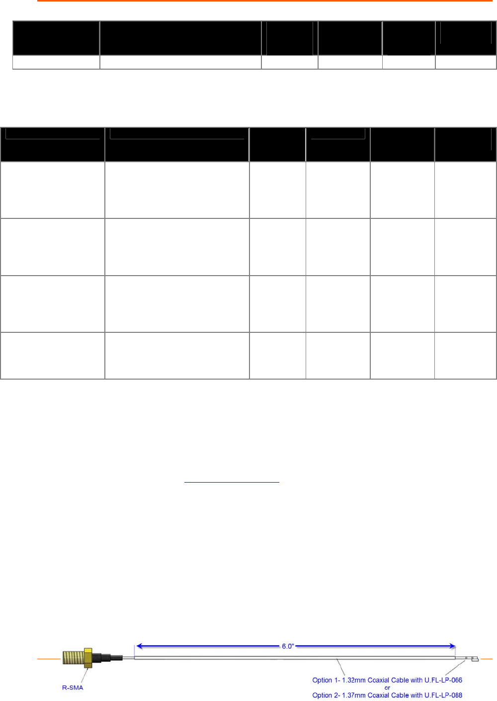
Lantronix provides a U.FL to Reverse SMA antenna cable in with the evaluation board and
sample kits for development work. These cables can be purchased from Lantronix for
production or supplied by an RF cable manufacturer. External antennas can be purchased
from an antenna vendor. Components for cable design should be selected for low loss over
the entire 2.4Ghz to 5.9Ghz signal range. The cable target impedance should be 50 ohms.
Figure 錯誤! 使用 [常用] 索引標籤將 Heading 1 套用到您想要在此處顯示的文字。-3 Reverse-SMA to U.FL
(Long) (Lantronix Part Number 500-180-R-ACC)
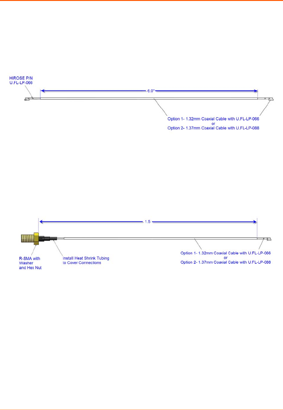
PW2050 Embedded Device Server Integration Guide 17
Figure 錯誤! 使用 [常用] 索引標籤將 Heading 1 套用到您想要在此處顯示的文字。-4 U.FL to U.FL Cable
(Lantronix Part Number 500-181-R-ACC)
Figure 錯誤! 使用 [常用] 索引標籤將 Heading 1 套用到您想要在此處顯示的文字。-5 Reverse-SMA to U.FL
(short) (Lantronix Part Number 500-182-R-ACC)
Antenna Placement
When designing the PW2050 Wi-Fi module to a mating board, it is important to consider the
final installation of the unit and its location with respect to connecting access points. The
antenna should be placed so that it has as clear as possible path to the connecting access
point for maximum range. Avoid placing the antenna such that it is blocked by metal walls or
ground planes of adjacent circuit boards.
When using the on board chip antenna it is recommended to place the module such that the
antenna region is along the edge of the board or extending outward from the edge of the board.
The area under the chip antenna region should be voided of all signals and planes
PW2050 Embedded Device Server Integration Guide 18
See the figure images below showing recommended placement with the module chip antenna.
Figure 錯誤! 使用 [常用] 索引標籤將 Heading 1 套用到您想要在此處顯示的文字。-6 Module with Chip
Antenna Board Edge Mounting
Note: The chip antenna region of the module shown in red above is at the top edge of
the PCB. The area in red should be voided to optimize antenna performance.
Using the RF1 Signal Pin
Instructions TBD.
Serial Interface
The PW2050 Wi-Fi SMT embedded device servers has two external serial interfaces. The
ExamplePCBPlacement
EdgeofPCB
Voidregioninred
6mmx23mm

PW2050 Embedded Device Server Integration Guide 19
signal levels on the serial interface are 3.3V tolerant. The serial interfaces require an external
transceiver in order to connect to external RS232, RS485, or RS422 networks. The signals of
the Serial Ports may be connected as shown in the reference schematic below. The
transceiver shown in the reference schematic is of type Exar, part number SP336. This
transceiver is a multiprotocol RS232, RS485, RS422 transceiver. Single protocol transceivers
may be used as required. The PW2050 interface may also be directly connected to the UART
interface of an external CPU.
Table 2-5 PW2050 Serial Port Signals
Signal Module Pin Description
TXD1 83 Serial Transmit Data output
RTS1 81 Serial Ready-to-Send / Serial Transmit enable
RXD1 82 Serial Receive Data input
CTS1 80 Serial Clear-to-Send
TXD2 79 Serial Transmit Data output 2
RTS2 24 Serial Ready-to-Send / Serial Transmit enable
RXD2 78 Serial Receive Data input 2
CTS2 25 Serial Clear-to-Send
Table 2-6 Example RS232 Connections (Serial Transceiver Required)
PW2050 Signal DTE Connector DCE Connector
Signal (Logic) Description DB9 DB25 Signal DB9 DB25 Signal
RXDx Data In 2 3 RXDx 3 2 TXDx
TXDx Data Out 3 2 TXDx 2 3 RXDx
RTSx H/W Flow Control Output 7 4 RTSx 8 5 CTSx
CTSx H/W Flow Control Input 8 5 CTSx 7 4 RTSx
CPx Modem Control Input 1 8 DCDx 4 20 DTRx
CPy Modem Control Output 4 20 DTRx 1 8 DCDx
Table 2-7 Example RS422/485 Connections (Serial Transceiver Required)
PW2050
Signal (logic) Description RS485
Signal DB25 4
Wire DB25 2
Wire DB9 4
wire DB9 2
wire
TXDx Data Out TX+485 14 14 7 7
TXDx Data Out TX-485 15 15 3 3
RXDx Data In RX+485 21 14 2 7
RXDx Data In RX-485 22 15 8 3
RTSx TX Enable
CPx RS485 Select
CPy RS485 2-wire

PW2050 Embedded Device Server Integration Guide 20
Note: The IO pins for PW2050 Wi-Fi SMT unit are set to floating input on power up until
configured by unit firmware. An external 100K ohm pull-up may be required on the serial transmit
signal to prevent downstream UART devices from detecting false characters on initial power up.
Ethernet Interface
The unit provides a 10/100 Mbps Ethernet interface for connection to an external network
through external magnetics and an external RJ45. The figure below shows the Ethernet
connections to a 10/100 Ethernet RJ45 Jack with Magnetics, J5 in the figure. The RJ45
Magnetic Jack is Belfuse part number 08B0-1D1T-06-F.
The Ethernet differential pair signals, ERXM/ERXP and ETXM/ETXP should be routed as 100-
ohm differential pairs on a layer next to the signal ground plane. The use of vias on these
signals should be minimized. Center tap signals RXCT and TXCT should be routed with at
least 20 mil trace thickness. The area underneath the RJ45 magnetic jack should be void of all
signals and planes. The connector shield should be connected to chassis. It is recommended
that 1206 resistor pads from chassis ground to signal ground be placed next to each of the
shield tabs. The resistor pads allow for 0 ohm jumper, ferrite beads, or decoupling caps to be
installed as needed for EMI/EMC improvement.
The Ethernet LED signals should be routed to discrete LEDs or to the LED pins on the RJ45
through 220 ohm or larger resistors. The LED signals are active low.
Also shown in the figure is an optional active choke that can be used to improve ESD, EFT,
and EMI/EMC performance in harsh environments. The device is shown as U22 in the figure
and is Akros part number AS1602. This device features route through pin assignments
allowing for the Ethernet differential signal pairs to be routed without altering the trace
impedance or adding vias. Due to this routing the device could be installed or depopulated as
needed. Lantronix has performed all certification to FCC Class B without U22 populated.
The Ethernet signals may be left unconnected if unused.
See the Lantronix app note, “How to Connect a Lantronix Embedded Module to a Wired
Ethernet Port” for more details on Ethernet connection and routing,
http://www.lantronix.com/pdf/appnotes/Connect-LTRX-Embed-Module-to-Wired-
Ethernet_AN.pdf.
Table 2-8 Ethernet Port Signals
Pin Name Description PW2050
Pins Signal Requirement RJ45 MagJack
Belfuse, 08B0-
1D1T-06-F Pin
assignment
ERXM Ethernet Receive Negative signal. 41 100 ohm differential
pair with ERXP
5
EXRP Ethernet Receive Positive signal. 40 100 ohm differential
pair with ERXM
4
ETXM Ethernet Transmit Negative
signal.
35 100 ohm differential
pair with ETXP
3

PW2050 Embedded Device Server Integration Guide 21
Pin Name Description PW2050
Pins Signal Requirement RJ45 MagJack
Belfuse, 08B0-
1D1T-06-F Pin
assignment
ETXP Ethernet Transmit Positive signal. 34 100 ohm differential
pair with ETXM
2
RXCT Center tap for receive pair. 38 Route > 20 mil width 6
TXCT Center tap for transmit pair 37 Route > 20 mil width 1
Chassis Unit chassis - RJ45 connector shield Shield tabs
E_LNKACT Link / activity LED. Active low.
Solid for link, blink for activity.
72 Route to LED cathode
through 220 ohm or
greater.
9
E_SPEED Link Speed Active low for
100Mbps, Off (high) for 10Mbps.
56 Route to LED cathode
through 220 ohm or
greater.
7
3V3 3.3 V power 3V3 3.3V power, connect to
LED anodes.
8, 10
USB Device Port
The PW2050 embedded device server has one USB 2.0 device port interface for connection to
an upstream USB device. The port consists of a differential pair, signals DDP and DDM.
These signals should be routed as a 90 ohm differential pair on a signal layer next to the signal
ground plane. The use of vias should be minimized on these signals. The USB signals can be
connected to a USB Mini Type B USB port or directly to an IC with a USB host port. If
connecting to an external port that is user accessible it is recommended to add a TVS diode
array to the signal nets for ESD protection. The ESD array shown in the figure is of type
SEMTECH RCIamp0502A. This device features through pin routing to minimize trace
impedance changes and simplify routing. The footprint for the TVS array can be added to the
PCB and the part can be depopulated if it is not needed. It is recommended that the power
drawn off the USB Mini Type B connector be limited to less than 500mA per USB requirements.
If the USB device port is unused the DDP and DDM pins may be left unconnected.
Table 2-9 USB Device Port Signals
Pin Name Description Module
Pins Signal
Requirement Mini Type B
USB Device
connector pin
USB+/DDP USB Device Port
Positive pin
18 Route as 90 ohm
differential pair with
DDM signal
3
USB-/DDM USB Device Port
Negative pin
19 Route as 90 ohm
differential pair with
DDP signal
2
5V 5V power from USB
cable
Current limit to 500
mA per port
1
Ground Signal Ground Ground Ground plane 5

PW2050 Embedded Device Server Integration Guide 22
USB Host Port
The PW2050 Module has two USB 2.0 Host port interfaces for connection to downstream USB
devices. Each port consists of a differential pair. Port USB2 is a high speed port and port
USB3 is a full speed port. These signals should be routed as 90 ohm differential pairs on a
signal layer next to the signal ground plane. The use of vias should be minimized on these
signals. The USB signals can be connected to a USB Type A dual USB port as shown in the
figure below or directly to an IC with a USB device port. If connecting to an external port that is
user accessible it is recommended to add a TVS diode array to the signal nets for ESD
protection. The ESD array shown in the figure is of type NXP, IP4234CZ6. If connecting to an
off board device that needs power add a USB power switch to current limit the 5V power
connection at the connector. USB requires that each port be limited to 500 mA maximum
sustained current. If using the USB host ports the end system must take into account the
amount of power consumed by the PW2050 module and each USB device connected to the
host ports. The schematic below shows how to connect 5V to a USB host connector using an
ST, STMPS2151 Power Distribution Switch. The USB host port 5V power is not provided by
the PW2050 module. If the USB host ports are unused their pins may be left unconnected.
Table 2-10 USB Host Port Signals
Pin Name
Description PW2050 Pins Signal
Requirement Type A USB
Host connector
pin
USB2+/HHSDPB USB HS Host Port
A Positive pin
21 Route as 90 ohm
differential pair
B3
USB2-/HHSDPM USB HS Host Port
A Negative pin
22 Route as 90 ohm
differential pair
B2
USB3+/HFSDPC USB FS Host Port
B Positive pin
52 Route as 90 ohm
differential pair
A3
USB3-/HFSDMC USB FS Host Port
B Negative pin
53 Route as 90 ohm
differential pair
A2
5V(User
supplied)
5V power for USB
connector
Current limit to
500 mA per port
A1, B1
Ground Signal Ground Ground Ground plane A4, B4
LEDs
The PW2050 embedded device server contains several external signals that are intended to
drive external status LEDs. The LEDs are listed below. The signals may be connected as
shown in the reference schematic figure below.
Note: The System LED usually remains on. When the Default button is pressed for 5-6
seconds, the System LED starts blinking every second to indicate the default button can
be released to complete resetting the unit to factory default. The unit reboots after
PW2050 Embedded Device Server Integration Guide 23
release of the Default button. A lit WLAN LED indicates the STA interface is associated
with an access point.
Table 2-11 PW2050 Wi-Fi Status LED Output Signals
Signal Pin Description
WI-FI LED 73 WI-FI Status LED, active low
SYS_LED 67 System status LED, active high
ETH SPEED 56 Ethernet 100Mbps ON (Active low), 10Mbps OFF
ETH LINK/ACT 72 Ethernet link ON (Active low)
Ethernet activity Blink (toggle)
General Purpose I/O Pins
PW2050 Wi-Fi SMT unit contains 13 pins which may be used as configurable inputs or outputs.
Listed below are the configurable I/O pins. These pins are 3.3V tolerant.
Table 2-12 Ethernet Interface PW2050 Serial Port Signals
Signal Pin Description
PW2050 Wi-Fi Reset
State
CP1 71 Configurable I/O Input
CP2/INT 68 Configurable I/O-SPI interrupt input Input
CP3 12 Configurable I/O- SPI MISO Input
CP4 13 Configurable I/O-SPI MOSI Input
CP5 16 Configurable I/O Input
CP6 17 Configurable I/O Input
CP7 14 Configurable I/O-SPI Clock Input
CP8 15 Configurable I/O-SPI Chip Select Input
CP9 26 Configurable I/O Input
CP10 60 Configurable I/O Input
CP11 59 Configurable I/O Input
CP12 58 Configurable I/O Input
CP13 57 Configurable I/O Input

PW2050 Embedded Device Server Integration Guide 24
Reset Pins
PW2050 embedded device servers have two signals for use as reset signals. Signal
EXT_RESET# is a hardware controlled input signal that will reboot the PW2050 processor
when asserted low. Signal DEFAULT# is polled by the PW2050 software. When DEFAULT#
is asserted low for six seconds, the unit will reset the system to the default manufacturing
settings and reboot the unit. PW2050 has an additional signal that can be used to wake up the
unit processor when the unit is in a sleep or power down state. The SHDN signal is active
when the module is in the shutdown state. Use the SHDN signal to gate off external logic
when the module is in the shutdown state to minimize power
Table 2-13 PW2050 Reset Signals
Signal Pin Description Reset
State
EXT_RESET# 77 Unit hardware reset, active low. Drive low for 50ms to
reboot unit. Signal should be driven high or left floating
after reset.
Input
DEFAULT# 66 Unit reset to default, active low.
Drive low for 5 to 6 seconds to reset unit to default
settings.
Input
WAKE 65 Toggle signal from low to high to WAKE from SLEEP or
Power down state
Input
SHDN 88 Active when module is in the shutdown state
3: PCB Footprint and Module Dimensions
The module recommended footprint is shown below. The antenna region should ideally be
placed on the edge of the board. The area under the antenna region should be void of all
signals and planes. The antenna location inside of the end unit and installation should be
chosen such that the antenna has as clear as possible line of site to the connecting WLAN
devices. The antenna path should be as clear as possible from metal, ground and power
planes from adjacent PCBs and other objects that can interfere with the signal path to the
connecting WLAN devices.
To Access CAD Files
1. Go to http://www.lantronix.com/products/cad-visio.html.
2. Click Download CAD files here to access the Registration Form.
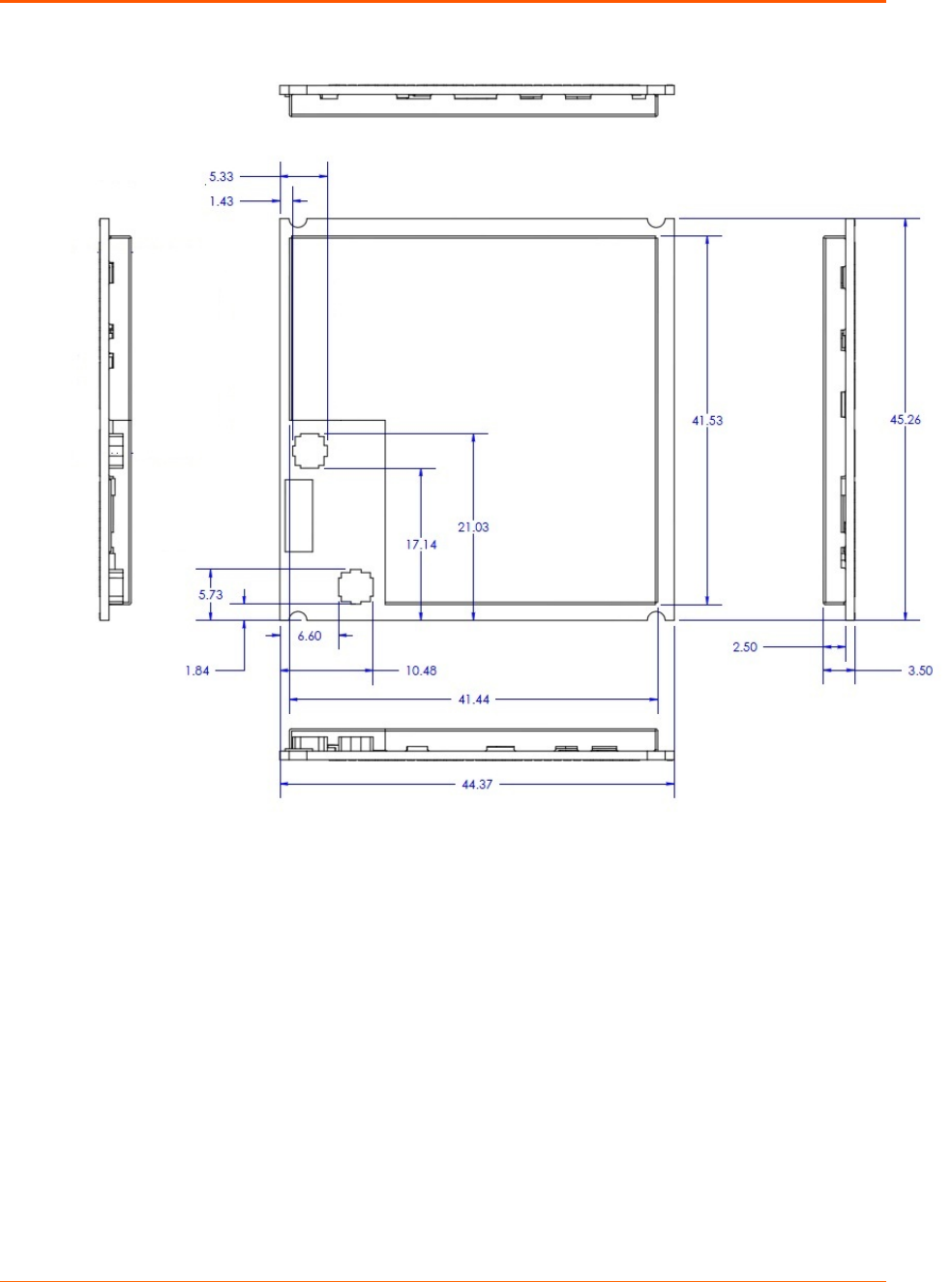
PW2050 Embedded Device Server Integration Guide 25
Figure 3-1 PW2050 Module Dimensions
PW2050 Embedded Device Server Integration Guide 26
Figure 錯誤! 使用 [常用] 索引標籤將 Heading 1 套用到您想要在此處顯示的文字。-2 PW2050
Recommended Footprint
The internal ground pads are used for module signal ground and thermal relief. The outer
layers should be flooded with ground and the ground pads should have many vias to the
internal ground layers.
Soldering coverage should be maximized and checked via x-ray for proper design. There is a
trade-off between providing enough soldering for conductivity and applying too much, which
allows the module to “float” on the pads creating reliability issues. Lantronix recommends 60%
or more full contact solder coverage on each of the internal ground pads after reflow. In
addition, Lantronix recommends that the solder wicks up at least 50% of the external LGA
pads for proper signal connection.
Solder Profile and Wash Instructions
The reflow profile is dependent on many factors including flux selection, solder composition,
and the capability of user's reflow equipment.
PW2050 Embedded Device Server Integration Guide 27
General guidelines are as follows:
The solder composition typically sets the peak temperatures of the profile. Recommend lead
free solder pastes SAC305: Type 4, water soluble or no clean are acceptable.
Reflow equipment needed at least nine heater zones. Recommend forced air type reflow oven
with nitrogen.
It is recommended that the peak temperature at the solder joint be within 235°C ~ 245°C and
the maximum component temperature should not exceed 245°C.
It is recommended that time above 217°C for the solder joints is between 40-90 seconds, and
with a minimum of 40 seconds.
Excessive ramp/cooling rates >3°C per second should be avoided.
To develop the reflow profile, it is recommended that the user place thermocouples at various
locations on the assembly to confirm that all locations meet the profile requirements. The
critical locations are the solder joints of SiP Module.
When developing the reflow profile, it is recommended that the actual fully loaded assembly be
used to make sure that the total thermal mass is accounted for.
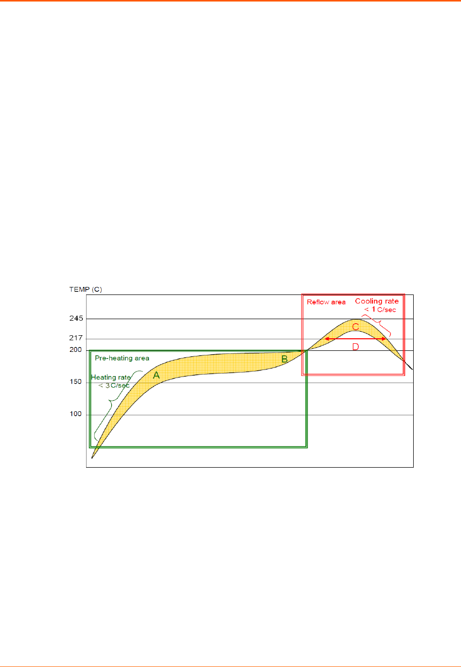
Figure 錯誤! 使用 [常用] 索引標籤將 Heading 1 套用到您想要在此處顯示的文字。-3 Recommended
Reflow Profile
(1) Solder paste alloy: SAC305(Sn96.5/Ag3.0/Cu0.5)(Lead free solder paste is recommended.)
(2) A-B. Temperature (pre-heat): 150~200°C; soak time: 60~120 seconds
(3) C. Peak temperature: 245°C
(4) D. Time above 217°C: 40~90 seconds
(5) Suggestion: Optimal cooling rate is 1°C per second from peak to 217°C
(6) Nine heater zones at least for reflow equipment.
(7) Nitrogen usage is recommended and the oxygen concentration is controlled less than 1500
parts per million.
Note: Need to inspect solder joint by X-ray post reflow.
PW2050 Embedded Device Server Integration Guide 28
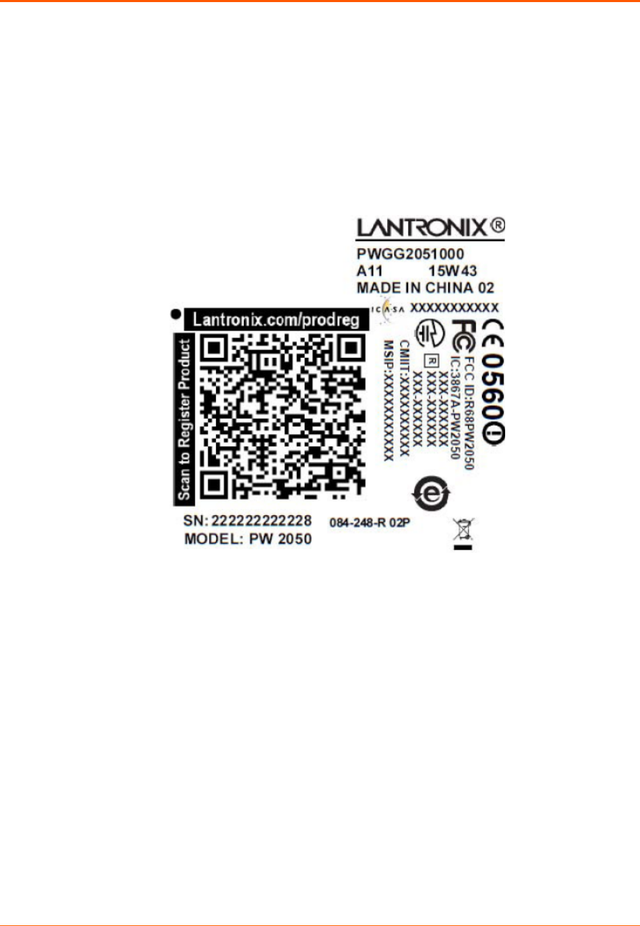
Product Information Label
The product information label contains important information about your specific unit, such as
its part number, revision, manufacturing date code, product model, country of origin,
datamatrix barcode and MAC address.
Figure 錯誤! 使用 [常用] 索引標籤將 Heading 1 套用到您想要在此處顯示的文字。-4 PW2050 Product
Label

PW2050 Embedded Device Server Integration Guide 29
Federal Communication Commission Interference Statement
This device complies with Part 15 of the FCC Rules. Operation is subject to the following two conditions: (1) This device may
not cause harmful interference, and (2) this device must accept any interference received, including interference that may
cause undesired operation.
This equipment has been tested and found to comply with the limits for a Class B digital device, pursuant to Part 15 of the
FCC Rules. These limits are designed to provide reasonable protection against harmful interference in a residential
installation. This equipment generates, uses and can radiate radio frequency energy and, if not installed and used in
accordance with the instructions, may cause harmful interference to radio communications. However, there is no guarantee
that interference will not occur in a particular installation. If this equipment does cause harmful interference to radio or
television reception, which can be determined by turning the equipment off and on, the user is encouraged to try to correct the
interference by one of the following measures:
- Reorient or relocate the receiving antenna.
- Increase the separation between the equipment and receiver.
- Connect the equipment into an outlet on a circuit different from that
to which the receiver is connected.
- Consult the dealer or an experienced radio/TV technician for help.
FCC Caution: Any changes or modifications not expressly approved by the party responsible for compliance could void the
user's authority to operate this equipment.
This transmitter must not be co-located or operating in conjunction with any other antenna or transmitter.
Operations in the 5.15-5.25GHz band are restricted to indoor usage only.
Radiation Exposure Statement:
This equipment complies with FCC radiation exposure limits set forth for an uncontrolled environment. This equipment should
be installed and operated with minimum distance 20cm between the radiator & your body.
This device is intended only for OEM integrators under the following conditions:
1) The antenna must be installed such that 20 cm is maintained between the antenna and users, and
2) The transmitter module may not be co-located with any other transmitter or antenna.

PW2050 Embedded Device Server Integration Guide 30
As long as 2 conditions above are met, further transmitter test will not be required. However, the OEM integrator is still
responsible for testing their end-product for any additional compliance requirements required with this module installed
IMPORTANT NOTE: In the event that these conditions can not be met (for example certain laptop configurations or co-
location with another transmitter), then the FCC authorization is no longer considered valid and the FCC ID can not be used
on the final product. In these circumstances, the OEM integrator will be responsible for re-evaluating the end product
(including the transmitter) and obtaining a separate FCC authorization.
End Product Labeling
This transmitter module is authorized only for use in device where the antenna may be installed such that 20 cm may be
maintained between the antenna and users. The final end product must be labeled in a visible area with the following:
“Contains FCC ID: R68PW2050”. The grantee's FCC ID can be used only when all FCC compliance requirements are met.
Manual Information To the End User
The OEM integrator has to be aware not to provide information to the end user regarding how to install or remove this RF
module in the user’s manual of the end product which integrates this module.
The end user manual shall include all required regulatory information/warning as show in this manual.
Industry Canada statement:
This device complies with RSS-247 of the Industry Canada Rules. Operation is subject to the following two conditions: (1) This
device may not cause harmful interference, and (2) this device must accept any interference received, including interference that
may cause undesired operation.
Ce dispositif est conforme à la norme CNR-247 d'Industrie Canada applicable aux appareils radio exempts de licence. Son
fonctionnement est sujet aux deux conditions suivantes: (1) le dispositif ne doit pas produire de brouillage préjudiciable, et (2) ce
dispositif doit accepter tout brouillage reçu, y compris un brouillage susceptible de provoquer un fonctionnement indésirable.
Radiation Exposure Statement:
This equipment complies with IC radiation exposure limits set forth for an uncontrolled environment. This equipment should be
installed and operated with minimum distance 20cm between the radiator & your body.
Déclaration d'exposition aux radiations:
Cet équipement est conforme aux limites d'exposition aux rayonnements IC établies pour un environnement non contrôlé. Cet
équipement doit être installé et utilisé avec un minimum de 20 cm de distance entre la source de rayonnement et votre corps.

PW2050 Embedded Device Server Integration Guide 31
This device is intended only for OEM integrators under the following conditions: (For module device use)
1) The antenna must be installed such that 20 cm is maintained between the antenna and users, and
2) The transmitter module may not be co-located with any other transmitter or antenna.
As long as 2 conditions above are met, further transmitter test will not be required. However, the OEM integrator is still responsible
for testing their end-product for any additional compliance requirements required with this module installed.
Cet appareil est conçu uniquement pour les intégrateurs OEM dans les conditions suivantes: (Pour utilisation de dispositif
module)
1) L'antenne doit être installée de telle sorte qu'une distance de 20 cm est respectée entre l'antenne et les utilisateurs, et
2) Le module émetteur peut ne pas être coïmplanté avec un autre émetteur ou antenne.
Tant que les 2 conditions ci-dessus sont remplies, des essais supplémentaires sur l'émetteur ne seront pas nécessaires. Toutefois,
l'intégrateur OEM est toujours responsable des essais sur son produit final pour toutes exigences de conformité supplémentaires
requis pour ce module installé.
IMPORTANT NOTE:
In the event that these conditions can not be met (for example certain laptop configurations or co-location with another transmitter),
then the Canada authorization is no longer considered valid and the IC ID can not be used on the final product. In these
circumstances, the OEM integrator will be responsible for re-evaluating the end product (including the transmitter) and obtaining a
separate Canada authorization.
NOTE IMPORTANTE:
Dans le cas où ces conditions ne peuvent être satisfaites (par exemple pour certaines configurations d'ordinateur portable ou de
certaines co-localisation avec un autre émetteur), l'autorisation du Canada n'est plus considéré comme valide et l'ID IC ne peut pas
être utilisé sur le produit final. Dans ces circonstances, l'intégrateur OEM sera chargé de réévaluer le produit final (y compris
l'émetteur) et l'obtention d'une autorisation distincte au Canada.
End Product Labeling
This transmitter module is authorized only for use in device where the antenna may be installed such that 20 cm may be maintained
between the antenna and users. The final end product must be labeled in a visible area with the following:
“Contains IC: 3867A-PW2050”.
Plaque signalétique du produit final

PW2050 Embedded Device Server Integration Guide 32
Ce module émetteur est autorisé uniquement pour une utilisation dans un dispositif où l'antenne peut être installée de telle sorte
qu'une distance de 20cm peut être maintenue entre l'antenne et les utilisateurs. Le produit final doit être étiqueté dans un endroit
visible avec l'inscription suivante: "Contient des IC: 3867A-PW2050".
Manual Information To the End User
The OEM integrator has to be aware not to provide information to the end user regarding how to install or remove this RF module in
the user’s manual of the end product which integrates this module.
The end user manual shall include all required regulatory information/warning as show in this manual.
Manuel d'information à l'utilisateur final
L'intégrateur OEM doit être conscient de ne pas fournir des informations à l'utilisateur final quant à la façon d'installer ou de
supprimer ce module RF dans le manuel de l'utilisateur du produit final qui intègre ce module.
Le manuel de l'utilisateur final doit inclure toutes les informations réglementaires requises et avertissements comme indiqué dans ce
manuel.
Caution :
(i) the device for operation in the band 5150-5250 MHz is only for indoor use to reduce the potential for harmful interference to co-
channel mobile satellite systems;
(ii) the maximum antenna gain permitted for devices in the bands 5250-5350 MHz and 5470-5725 MHz shall be such that the
equipment still complies with the e.i.r.p. limit;
(iii) the maximum antenna gain permitted for devices in the band 5725-5850 MHz shall be such that the equipment still complies with
the e.i.r.p. limits specified for point-to-point and non-point-to-point operation as appropriate; and
(iv) Users should also be advised that high-power radars are allocated as primary users (i.e. priority users) of the bands 5250-5350
MHz and 5650-5850 MHz and that these radars could cause interference and/or damage to LE-LAN devices.
Avertissement:
Le guide d’utilisation des dispositifs pour réseaux locaux doit inclure des instructions précises sur les restrictions susmentionnées,
notamment :

PW2050 Embedded Device Server Integration Guide 33
(i) les dispositifs fonctionnant dans la bande 5150-5250 MHz sont réservés uniquement pour une utilisation à l’intérieur afin de
réduire les risques de brouillage préjudiciable aux systèmes de satellites mobiles utilisant les mêmes canaux;
(ii) le gain maximal d'antenne permis pour les dispositifs utilisant les bandes de 5250 à 5 350 MHz et de 5470 à 5725 MHz doit être
conforme à la limite de la p.i.r.e;
(iii) le gain maximal d'antenne permis (pour les dispositifs utilisant la bande de 5 725 à 5 850 MHz) doit être conforme à la limite de la
p.i.r.e. spécifiée pour l'exploitation point à point et l’exploitation non point à point, selon le cas;
(iv) De plus, les utilisateurs devraient aussi être avisés que les utilisateurs de radars de haute puissance sont désignés utilisateurs
principaux (c.-à-d., qu’ils ont la priorité) pour les bandes 5250-5350 MHz et 5650-5850 MHz et que ces radars pourraient causer du
brouillage et/ou des dommages aux dispositifs LAN-EL.
Europe – EU Declaration of Conformity
This device complies with the essential requirements of the R&TTE Directive 1999/5/EC. The following test methods have been
applied in order to prove presumption of conformity with the essential requirements of the R&TTE Directive 1999/5/EC:
(Safety)
EN 60950-1:2005 (Second Edition); Am1:2009 + Am2:2013
Safety of Information Technology Equipment
(MPE)
- EN 62311:2008
Assessment of electronic and electrical equipment related to human exposure restrictions for electromagnetic fields (0 Hz-300
GHz) (IEC 62311:2007 (Modified))
(Radio)
EN 300 328 V1.9.1:2015
Electromagnetic compatibility and Radio spectrum Matters (ERM); Wideband transmission systems; Data transmission equipment
operating in the 2.4GHz ISM band andusing wide band modulation techniques; Harmonized EN covering the essential
requirements of article 3.2 of the R&TTE Directive
- EN 301 893 V1.8.1:2015
PW2050 Embedded Device Server Integration Guide 34
Broadband Radio Access Networks (BRAN); 5GHz high performance RLAN; Harmonized EN covering the essential requirements
of article 3.2 of the R&TTE Directive
(EMC)
- EN 301 489-1 V1.9.2:2011
Electromagnetic compatibility and Radio spectrum Matters (ERM); ElectroMagnetic Compatibility (EMC) standard for radio
equipment and services; Part 1: Common technical requirements
- EN 301 489-3 V1.6.1:2013
Electromagnetic compatibility and Radio spectrum Matters (ERM); ElectroMagnetic Compatibility (EMC) standard for radio
equipment and services; Part 3: Specific conditions for Short-Range Devices (SRD) operating on frequencies between 9 kHz and
246 GHz
- EN 301 489-17 V2.2.1:2012
Electromagnetic compatibility and Radio spectrum Matters (ERM); ElectroMagnetic Compatibility (EMC) standard for radio
equipment; Part 17: Specific conditions for Broadband Data Transmission Systems
<Insert CE mark + notified body number + alert mark here>
(除5G 未調和要放驚嘆號)
Česky
[Czech]
[Jméno výrobce] tímto prohlašuje, že tento [typ zařízení] je ve shodě se základními
požadavky a dalšími příslušnými ustanoveními směrnice 1999/5/ES.
Dansk
[Danish]
Undertegnede [fabrikantens navn] erklærer herved, at følgende udstyr [udstyrets
typebetegnelse] overholder de væsentlige krav og øvrige relevante krav i direktiv
1999/5/EF.
Deutsch
[German]
Hiermit erklärt [Name des Herstellers], dass sich das Gerät [Gerätetyp] in
Übereinstimmung mit den grundlegenden Anforderungen und den übrigen einschlägigen
Bestimmungen der Richtlinie 1999/5/EG befindet.
Eesti
[Estonian]
Käesolevaga kinnitab [tootja nimi = name of manufacturer] seadme [seadme tüüp = type
of equipment] vastavust direktiivi 1999/5/EÜ põhinõuetele ja nimetatud direktiivist

PW2050 Embedded Device Server Integration Guide 35
tulenevatele teistele asjakohastele sätetele.
English Hereby, [name of manufacturer], declares that this [type of equipment] is in compliance
with the essential requirements and other relevant provisions of Directive 1999/5/EC.
Español
[Spanish]
Por medio de la presente [nombre del fabricante] declara que el [clase de equipo]
cumple con los requisitos esenciales y cualesquiera otras disposiciones aplicables o
exigibles de la Directiva 1999/5/CE.
Ελληνική
[Greek]
ΜΕ ΤΗΝ ΠΑΡΟΥΣΑ [name of manufacturer] ∆ΗΛΩΝΕΙ ΟΤΙ [type of equipment]
ΣΥΜΜΟΡΦΩΝΕΤΑΙ ΠΡΟΣ ΤΙΣ ΟΥΣΙΩ∆ΕΙΣ ΑΠΑΙΤΗΣΕΙΣ ΚΑΙ ΤΙΣ ΛΟΙΠΕΣ ΣΧΕΤΙΚΕΣ
∆ΙΑΤΑΞΕΙΣ ΤΗΣ Ο∆ΗΓΙΑΣ 1999/5/ΕΚ.
Français
[French]
Par la présente [nom du fabricant] déclare que l'appareil [type d'appareil] est conforme
aux exigences essentielles et aux autres dispositions pertinentes de la directive
1999/5/CE.
Italiano
[Italian]
Con la presente [nome del costruttore] dichiara che questo [tipo di apparecchio] è
conforme ai requisiti essenziali ed alle altre disposizioni pertinenti stabilite dalla direttiva
1999/5/CE.
Latviski
[Latvian]
Ar šo [name of manufacturer / izgatavotāja nosaukums] deklarē, ka [type of equipment /
iekārtas tips] atbilst Direktīvas 1999/5/EK būtiskajām prasībām un citiem ar to
saistītajiem noteikumiem.
Lietuvių
[Lithuanian]
Šiuo [manufacturer name] deklaruoja, kad šis [equipment type] atitinka esminius
reikalavimus ir kitas 1999/5/EB Direktyvos nuostatas.
Nederlands
[Dutch]
Hierbij verklaart [naam van de fabrikant] dat het toestel [type van toestel] in
overeenstemming is met de essentiële eisen en de andere relevante bepalingen van
richtlijn 1999/5/EG.
Malti
[Maltese]
Hawnhekk, [isem tal-manifattur], jiddikjara li dan [il-mudel tal-prodott] jikkonforma mal-
ħtiġijiet essenzjali u ma provvedimenti oħrajn relevanti li hemm fid-Dirrettiva 1999/5/EC.
Magyar
[Hungarian]
Alulírott, [gyártó neve] nyilatkozom, hogy a [... típus] megfelel a vonatkozó alapvetõ
követelményeknek és az 1999/5/EC irányelv egyéb elõírásainak.
Polski
[Polish]
Niniejszym [nazwa producenta] oświadcza, że [nazwa wyrobu] jest zgodny z
zasadniczymi wymogami oraz pozostałymi stosownymi postanowieniami Dyrektywy
1999/5/EC.
Português
[Portuguese]
[Nome do fabricante] declara que este [tipo de equipamento] está conforme com os
requisitos essenciais e outras disposições da Directiva 1999/5/CE.
Slovensko [Ime proizvajalca] izjavlja, da je ta [tip opreme] v skladu z bistvenimi zahtevami in ostalimi

PW2050 Embedded Device Server Integration Guide 36
[Slovenian] relevantnimi določili direktive 1999/5/ES.
Slovensky
[Slovak]
[Meno výrobcu] týmto vyhlasuje, že [typ zariadenia] spĺňa základné požiadavky a všetky
príslušné ustanovenia Smernice 1999/5/ES.
Suomi
[Finnish]
[Valmistaja = manufacturer] vakuuttaa täten että [type of equipment = laitteen
tyyppimerkintä] tyyppinen laite on direktiivin 1999/5/EY oleellisten vaatimusten ja sitä
koskevien direktiivin muiden ehtojen mukainen.
Svenska
[Swedish]
Härmed intygar [företag] att denna [utrustningstyp] står I överensstämmelse med de
väsentliga egenskapskrav och övriga relevanta bestämmelser som framgår av direktiv
1999/5/EG.
查詢 NB no.
http://ec.europa.eu/enterprise/newapproach/nando/index.cfm?fuseaction=notifiedbody.main