lantronix WIPORTG WIRELESS EMBEDDED DEVICE SERVER User Manual integration guide
lantronix WIRELESS EMBEDDED DEVICE SERVER integration guide
Contents
- 1. integration guide
- 2. users guide
- 3. USERS GUIDE
integration guide

WiPort™ Integration Guide
Part Number 900-333
Revision G June 2006

Copyright and Trademark
© 2005, 2006, Lantronix. All rights reserved. No part of the contents of this book may
be transmitted or reproduced in any form or by any means without the written
permission of Lantronix. Printed in the United States of America.
WiPort, with its patent-pending technology, is a trademark of Lantronix.
Ethernet is a trademark of XEROX Corporation. UNIX is a registered trademark of
The Open Group. Windows 95, Windows 98, Windows 2000, Windows NT, and
Windows XP are trademarks of Microsoft Corp. Netscape is a trademark of Netscape
Communications Corporation.
Contacts
Lantronix Corporate Headquarters
15353 Barranca Parkway
Irvine, CA 92618, USA
Phone:949-453-3990
Fax: 949-453-3995
Technical Support
Phone: 800-422-7044 or 949-453-7198
Fax: 949-450-7226
Online: www.lantronix.com/support
Email support@lantronix.com
Sales Offices
For a current list of our domestic and international sales offices, go to the Lantronix
web site at www.lantronix.com/about/contact/

WiPort™ Integration Guide 3
Disclaimer
This equipment has been tested and found to comply with the limits for a Class B
digital device, pursuant to Part 15 of the FCC Rules. These limits are designed to
provide reasonable protection against harmful interference in a residential
installation. This equipment generates, uses and can radiate radio frequency energy
and, if not installed and used in accordance with the instructions, may cause harmful
interference to radio communications. However, there is no guarantee that
interference will not occur in a particular installation. If this equipment does cause
harmful interference to radio or television reception, which can be determined by
turning the equipment off and on, the user is encouraged to try to correct the
interference by one of the following measures:
Reorient or relocate the receiving antenna.
Increase the separation between the equipment and receiver.
Connect the equipment into an outlet on a circuit different from that to which
the receiver is connected.
Consult the dealer or an experienced radio/TV technician for help.
This device complies with Part 15 of the FCC Rules. Operation is subject to the
following two conditions: (1) This device may not cause harmful interference, and (2)
this device must accept any interference received, including interference that may
cause undesired operation.
This device is intended only for OEM Integrators. The OEM integrator should be
aware of the following important issues.
Labeling of the End Product
The end product to integrate this module has to be clearly identified on the label that
this end product contains an FCC approved RF module. The format of such
statement could be "Contains Transmitter with FCC ID: R68WIPORTG" or similar.
Integration Note
a) This module is authorized under limited module approval specified to mobile host
equipment. So, the antenna must be installed such that 20cm is maintained between
the antenna and users.
b) The transmitter module may not be co-located with any other transmitter or
antenna.
As long as the 2 conditions above are met, further transmitter testing will not be
required. However, the OEM integrator is still responsible for testing their end-product
for any additional compliance requirements required with this module installed (for
example, digital device emission, PC peripheral requirements, etc.)
Note: In the event that these conditions can not be met (for example certain
laptop configurations, general purpose PCMCIA or similar cards, or co-
location with another transmitter), then the FCC authorization is no longer
considered valid and the FCC ID can not be used on the final product
(including the transmitter) and obtaining a separate FCC authorization.
Note: Changes or modifications to this device not explicitly approved by Lantronix will
void the user's authority to operate this device.

WiPort™ Integration Guide 4
Contents
1: Introduction 6
About the Integration Guide________________________________________________6
Additional Documentation _________________________________________________6
2: Description and Specifications 7
WiPort Overview ________________________________________________________7
WiPort Block Diagram ____________________________________________________8
PCB Interface __________________________________________________________9
Mating Connector ______________________________________________________10
Serial Input/Output______________________________________________________10
Sample Layouts for RS-485 Connectivity ____________________________________12
WLAN Input/Output _____________________________________________________13
Ethernet Input/Output ___________________________________________________13
Power, Ground, and Reset _______________________________________________14
Absolute Maximum Ratings_______________________________________________14
Recommended Operating Conditions _______________________________________14
Ethernet PHY Receiver Input Characteristics (RX+, RX-) ________________________15
100Base-TX Transceiver Characteristics (TX+, TX-) ___________________________15
Wireless Specifications __________________________________________________15
Technical Specifications _________________________________________________17
Dimensions ___________________________________________________________18
Recommended PCB Layout ______________________________________________19
Product Information Label ________________________________________________20
3: Development Kit 21
Contents of the Kit ______________________________________________________21
Evaluation Board Description _____________________________________________21
Serial Interfaces________________________________________________________21
Power Supply _________________________________________________________22
General Control PLD ____________________________________________________22
Configuration Switch Bank _______________________________________________22
Evaluation Board Layout _________________________________________________23
Evaluation Board Schematics _____________________________________________24
Compliance Information__________________________________________________28
Warranty _____________________________________________________________29

WiPort™ Integration Guide 5
List of Figures
Figure 2-1. WiPort Block Diagram...........................................................................................8
Figure 2-2. Combined RS-232/485 Transceiver ...................................................................12
Figure 2-3. Separate RS-232/485 Transceivers ...................................................................12
Figure 2-4. Separate RS-485 Transceivers for 2-Wire and 4-Wire Setups...........................13
Figure 2-5. Side Views..........................................................................................................18
Figure 2-6. Top View.............................................................................................................18
Figure 2-7. Bottom View........................................................................................................19
Figure 2-8. PCB Layout.........................................................................................................19
Figure 2-9. Product Label......................................................................................................20
Figure 3-1. WiPort Evaluation Board Layout.........................................................................23
Figure 3-2. Evaluation Board Schematics.............................................................................24
List of Tables
Table 2-1. PCB Interface Signals............................................................................................9
Table 2-2. Mating Connectors...............................................................................................10
Table 2-3. Channel 1 Connections........................................................................................11
Table 2-4. Channel 2 Connections........................................................................................11
Table 2-5. Channel 2 RS-422/485 4-Wire Connections........................................................11
Table 2-6. Channel 2 RS-485 2-Wire Connections...............................................................11
Table 2-7. WLAN Signals......................................................................................................13
Table 2-8. Ethernet Signals...................................................................................................13
Table 2-9. Power, Ground, and Reset Pins ..........................................................................14
Table 2-10. Absolute Maximum Ratings ...............................................................................14
Table 2-11. Operating Conditions, Serial Ports, & Configurable Pins...................................14
Table 2-12. Ethernet Input Characteristics............................................................................15
Table 2-13. 100Base-TX Transceiver Attributes ...................................................................15
Table 2-14. Wireless Specifications......................................................................................15
Table 2-15. Technical Specifications ....................................................................................17
Table 3-1. RS-232 Signals....................................................................................................22
Table 3-2. Channel 2 RS-485 4-Wire Connector ..................................................................22
Table 3-3. Channel 2 RS-485 2-Wire Connector ..................................................................22
Table 3-4. Jumper Configurations.........................................................................................22
Table 3-5. Configurable Pin Configurations ..........................................................................23

WiPort™ Integration Guide 6
1
1:
:
I
In
nt
tr
ro
od
du
uc
ct
ti
io
on
n
About the Integration Guide
This guide provides the information needed to integrate the WiPort device server
within another product. The intended audiences are the engineers responsible for
integrating the WiPort into their product.
Additional Documentation
The following guides are available on the product CD and the Lantronix Web site
(www.lantronix.com)
WiPort™ Development Kit
Quick Start Guide
Briefly explains the basics to get the WiPort up
and running.
WiPort™ User Guide Provides information needed to configure, use,
and update the WiPort firmware.

WiPort™ Integration Guide 7
1
1.
.2
2:
:
D
De
es
sc
cr
ri
ip
pt
ti
io
on
n
a
an
nd
d
S
Sp
pe
ec
ci
if
fi
ic
ca
at
ti
io
on
ns
s
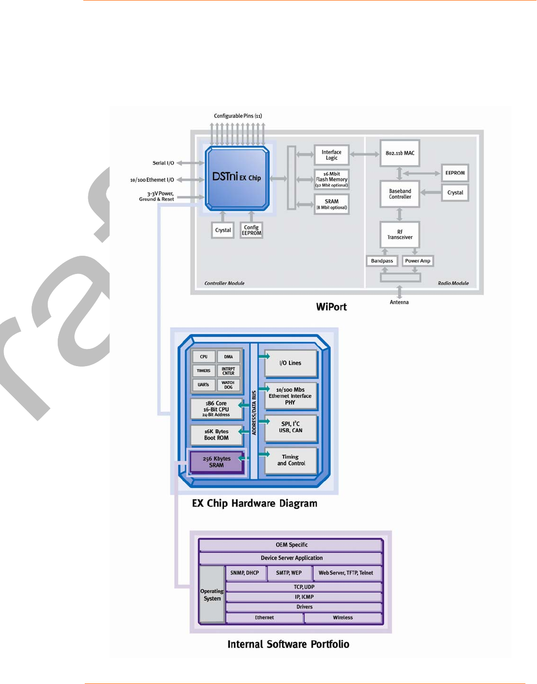
The WiPort wireless embedded device server is a complete network-enabling
solution based on the IEEE 802.11b/g wireless standard, with WPA and WEP
capabilities. WiPort allows Original Equipment Manufacturers (OEMs) to add
wireless connectivity to their products by incorporating it onto a circuit board with
minimal engineering.
The WiPort functions independently of a PC, providing an integrated solution that
combines a processor, memory, 802.11b/g transceiver and dual high-speed serial
ports into a single compact module. It includes a wireless connection, an operating
system, an embedded Web server, and a full TCP/IP protocol stack. In addition, the
WiPort sends email alerts and supports numerous other network communication
protocols, including ARP, UDP, TCP, ICMP, Telnet, AutoIP, DHCP, HTTP and
SNMP.
WiPort Overview
The WiPort contains Lantronix’s own DSTni controller with 256 Kbytes of internal
zero wait state SRAM, 16 Kbytes of boot ROM, and integrated 10/100 PHY.
The WiPort also contains the following:
Two 3.3-volt v24 serial interfaces (5V tolerant)
Up to 921600 Baud
16 or 32Mbit flash memory (with optional additional 8Mbit SRAM)
88 MHz clock
802.11b interface
11 configurable pins
10/100 Ethernet interface
The WiPort requires +3.3-volt power and is designed to operate within a temperature
range of -30ºC to +70ºC.
Description and Specifications
WiPort™ Integration Guide 8
WiPort Block Diagram
The following drawing is a block diagram of the WiPort showing the relationships of
the components.
Figure 2-1. WiPort Block Diagram

Description and Specifications
WiPort™ Integration Guide 9
PCB Interface
Table 2-1. PCB Interface Signals
Pin Number WiPort Pin
Function
Notes
1 3.3V Power Supply input
2 3.3V Power Supply input
3 RTS0 Request “to send” hardware
flow control output (logic
level), serial port 0
4 TXD0 Transmit data output (logic
level), serial port 0
5 RXD0 Receive data input (logic
level), serial port 0
6 CP2 Configurable pin
7 CP3 Configurable pin.
8 CTS0 Clear “to send” hardware flow
control input (logic level),
serial port 0
9 CP10 Configurable pin
10 CP8 Configurable pin
11 Signal Ground
12 Signal Ground
13 Reset In Resets the WiPort unit. Reset
In is low active. Minimum
reset pulse width is 2ms at IIL
= -500 µA
14 CP0 Configurable pin
15 RTS1 Request “to send” hardware
flow control output (logic
level), serial port 1
16 TXD1 Transmit data output (logic
level), serial port 1
17 RXD1 Receive data input (logic
level), serial port 1
18 CP9 Configurable pin
19 CP4 Configurable pin
20 CTS1 Clear “to send” hardware flow
control input (logic level),
serial port 1
21 Reserved Reserved for future use
22 Reserved Reserved for future use
23 Signal Ground
24 Signal Ground
25 Reserved Reserved for future use
26 Reserved Reserved for future use
27 Ethernet Status
LED2
Ethernet activity
28 Ethernet Status
LED1
Ethernet link
29 Ethernet TX- Output
30 Ethernet TX+ Output

Description and Specifications
WiPort™ Integration Guide 10
Pin Number WiPort Pin
Function
Notes
31 Ethernet RX Center
Tap
32 Ethernet TX Center
Tap
33 Ethernet RX- Input
34 Ethernet RX+ Input
35 CP1 Configurable pin
36 WLAN Power LED
(WiPort B only)
High active output, tristated in
Ethernet mode
37 CP6 Configurable pin
38 CP5 Configurable pin.
39 WLAN Activity LED High active output, tristated in
Ethernet mode
40 CP7 Configurable pin
Note: For all the configurable pins, see the WiPort User Guide for selectable
functions.
Mating Connector
Table 2-2. Mating Connectors
Mating Connector Description
Recommended: Samtec FTMH-120-03-F-DV-ES (shrouded
header)
Alternative: Samtec FTMH-120-03-F-DV (not shrouded)
Alternative: Oupiin 2411-2X20GDN/017 (not shrouded)
The mating connector is
a 1mm micro header,
40 pins,
2 x 20.
Serial Input/Output
The unit has two serial ports compatible with V24 serial standards at data rates up to
921Kbps. The serial I/O signals are 3.3V CMOS logic level and pins are 5V tolerant.
Serial signals connect to an internal device, such as a UART. For evaluation and
prototype work, it is convenient to have an external RS-232 interface that can
connect to the serial port on a PC. The WiPort Evaluation Board has one RS-232
and one RS-232/422/485 transceiver (level shifters) to implement this external
interface (only the WiPort 485 supports the RS-422/485 interface).
If desired, use the CPs to create a DTE or DCE-style interface using any 3 available
CPs. To create these interfaces, connect the signals according to Table 2-3 and
Table 2-4.
Note: CPx, CPy, and CPz are any of the available CPs.

Description and Specifications
WiPort™ Integration Guide 11
Table 2-3. Channel 1 Connections
WiPort DCE Connector DTE Connector
Signal Description
DB9 DB25 Signal DB9 DB25 Signal
RXD0 Data In 2 3 RXD0 3 2 TXD0
TXD0 Data Out 3 2 TXD0 2 3 RXD0
RTS0 H/W Flow Control
Output
7 4 RTS0 8 5 CTS0
CTS0 H/W Flow Control Input 8 5 CTS0 7 4 RTS0
CPx Modem Control Input 1 8 DCD 4 20 DTR
CPy Modem Control Output 4 20 DTR 1 8 DCD
CPz LED
Table 2-4. Channel 2 Connections
WiPort DCE Connector DTE Connector
Signal Description
DB9 DB25 Signal DB9 DB25 Signal
RXD1 Data In 2 3 RXD0 3 2 TXD1
TXD1 Data Out 3 2 TXD0 2 3 RXD1
RTS1 H/W Flow Control
Output
7 4 RTS0 8 5 CTS1
CTS1 H/W Flow Control Input 8 5 CTS0 7 4 RTS1
CPx Modem Control Input 1 8 DCD 4 20 DTR
CPy Modem Control Output 4 20 DTR 1 8 DCD
CPz LED
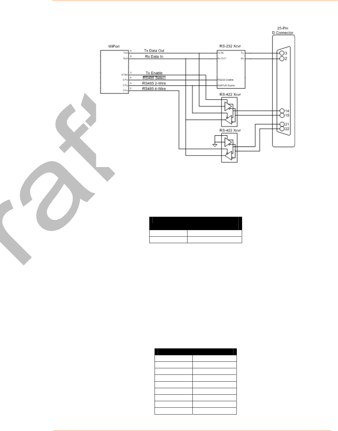
Table 2-5. RS-422/485 4-Wire Connections
WiPort
Signal
Description
DB25 Pinout DB9 Pinout
TX+ TX+ 14 7
TX- TX- 15 3
RX+ RX+ 21 2
RX- RX- 22 8
RTS TX Enable
CPx RS-485 Select
CPy RS-485 2-wire
CPz RS-485 4-wire
Table 2-6. RS-485 2-Wire Connections
WiPort
Signal
Description
DB25 Pinout DB9 Pinout
TX+/RX+ TX+/RX+ 14 7
TX-/RX- TX-/RX- 15 3
RTS TX Enable
CPx RS-485 Select
CPy RS-485 2-wire
CPz RS-485 4-wire
Description and Specifications
WiPort™ Integration Guide 12
Sample Layouts for RS-485 Connectivity
Figure 2-2. Combined RS-232/422 Transceiver
Figure 2-3. Separate RS-232/422 Transceivers
Description and Specifications
WiPort™ Integration Guide 13
Figure 2-4. Separate RS-422 Transceivers for 2-Wire and 4-Wire Setups
WLAN Input/Output
The following table displays the WLAN input and output functions.
Table 2-7. WLAN Signals
Pin Number Pin Function
36 WLAN Power LED
39 WLAN Activity LED
WLAN Power LED can be used to drive an external LED to monitor the status of the
radio. When the WLAN Power LED is on continuously, it indicates the radio is on
and in normal mode. When it is blinking, it indicates the radio is in power saving
mode.
WLAN Activity LED is also used to drive an external LED to monitor the status of the
radio. When the LED is blinking, it is receiving or transmitting wireless data. When it
is off, it indicates there is no wireless activity.
Ethernet Input/Output
The following table displays the Ethernet input and output functions.
Table 2-8. Ethernet Signals
Pin Number Pin Function
Ethernet
30 TX+
29 TX-
32 TX Center Tap
34 RX+
33 RX-
31 RX Center Tap
28 Status LED1
27 Status LED2

Description and Specifications
WiPort™ Integration Guide 14
Ethernet communication lines connect to external magnetics and an external RJ-45
jack. They are used for the creation of an Ethernet interface (instead of using the
wireless interface). Either Ethernet or WLAN is selectable for communication (not
both).
Ethernet Link LED 1 can be used to drive an external LED. The LED is on when a
link exists.
Ethernet Activity LED 2 is also used to drive an external LED. The LED blinks when
activity is present.
Power, Ground, and Reset
Table 2-9. Power, Ground, and Reset Pins
Power Ground Reset
Pin 1 Pin 11 Pin 13
Pin 2 Pin 12
Pin 23
Pin 24
Driving the Reset In line low resets the WiPort. Minimum reset pulse width is 2ms at
IIL = -500uA
Absolute Maximum Ratings
Table 2-10. Absolute Maximum Ratings
Parameter Min Max Units
Supply Voltage 3.0 3.6 V
Input Voltage -0.5 6 V
Output Voltage -0.5 6 V
Operating Temperature -30 70 ºC
Storage Temperature -40 85 ºC
Recommended Operating Conditions
The following table illustrates the optimal and recommended operating conditions for
the WiPort device.
Table 2-11. Operating Conditions, Serial Ports, & Configurable Pins
Parameter Min Typical Max Units
Supply Voltage 3.135 3.3 3.45 V
Voltage Ripple 2 %
VIL Input Low Voltage* -0.3 0.8 V
VIH Input High Voltage* 2 5.5 V
II Input Leakage Current* +/- 10 nA +/- 1 µA
VOL Output Low Voltage @ IOL max* 0.4 V
VOH Output High Voltage @ IOH max* 2.4 V
TXD0, RTS0, TXD1, RTS1 IOL
Low Level Output Current @ VOL 0.4V
2.2 3.5 4.3 mA
CP0-CP10 Low Level Output Current
@VOL 0.4V
4.4 7.1 8.5 mA
TXD0, RTS0, TXD1, RTS1 IOH
High Level Output Current @ VOH 2.4V
-3.2 -6.4 -10.0 mA
CP0-CP10 IOH
High Level Output Current @ VOH 2.4V
-6.4 -12.8 -20.0 mA
* For UART and CP pins

Description and Specifications
WiPort™ Integration Guide 15
Ethernet PHY Receiver Input Characteristics (RX+, RX-)
Table 2-12. Ethernet Input Characteristics
Parameter Specification Units Comments
Full Scale Input Voltage 3.0 differential pk-to-pk V
Input Common Mode 1.6 – 2.0 V Gain dependent
100Base-TX Transceiver Characteristics (TX+, TX-)
The following table displays the 100Base-TX transceiver characteristics.
Table 2-13. 100Base-TX Transceiver Attributes
Parameter Sym Min Typical Max Units
Peak Differential Output Voltage VP 0.95 1.05 V
100M TX mid-level -50 50 mV
Signal Amplitude Symmetry VSS 98 102 %
Signal Rise/Fall Time TRF 3.0 5.0 ns
Rise/Fall Time Symmetry TRFS 0.5 ns
Duty Cycle Distortion DCD 35 50 65 %
Overshot/Undershot VOS 5 %
Jitter (measured differentially) 1.4 ns
Ethernet LED1, LED2 current 8.8 14.1 17.0 mA
Wireless Specifications
Refer to the following table for the WiPort’s wireless specifications:
Table 2-14. Wireless Specifications
Category IEEE 802.11b IEEE 802.11b
Frequency Range 2.412 – 2.484
GHz
2.412 – 2.484
GHz
Output Power 14 +/- 1.0
dBm
14 +/- 1.0 dBm
<= 12 Mbps
12 +/- 1.0 dBm
> 12 Mbps
Antenna Connector 1 1
Data Rates 1,2,5.5,11
Mbps
(802.11b HR)
1*,2*,5.5*,11*,6,
9,12,18*,24*,36*
,48,54* Mbps
Number of Selectable
Subchannels**
US 1-11
CA 1-11
JP 1-14
FR 10-13
SP 10-11
OT 1-13
(OT=Others)
US 1-11
CA 1-11
JP 1-14
FR 10-13
SP 10-11
OT 1-13
(OT=Others)
Modulation DSSS,DBPS
K,DQPSK,C
CK
DSSS,DBPSK,
DQPSK,CCK,
OFDM, 16QAM,
64QAM
Radio
Antenna Connector 1 1
Security WEP
64/128,WPA
WEP
64/128,WPA
Maximum Receive Level 10 dBm
(
with 10 dBm
(
with

Description and Specifications
WiPort™ Integration Guide 16
Category IEEE 802.11b IEEE 802.11b
PER < 8%) PER < 8%)
Receiver Sensitivity 82 dBm for
11 Mbps
87 dBm for
5.5 Mbps
89 dBm for
2.0 Mbps
93 dBm for
1.0 Mbps
72 dBm for 54
Mbps
87 dBm for 11
Mbps
89 dBm for 5.5
Mbps
90 dBm for 2.0
Mbps
92 dBm for 1.0
Mbps
WLAN Power and Link LED Current Max: 4 mA Max: 4 mA

Description and Specifications
WiPort™ Integration Guide 17
Technical Specifications
Table 2-15. Technical Specifications
Category WiPort B WiPort G
CPU, Memory Lantronix DSTni-EX 186 CPU, 256 KB zero
wait state SRAM
2048 KB Flash or 4096 KB Flash, 16 KB Boot
ROM, 1024 KB SRAM
Lantronix DSTni-EX 186 CPU, 256 KB zero
wait state SRAM
2048 KB Flash or 4096 KB Flash, 16 KB
Boot ROM, 1024 KB SRAM
Firmware Upgradeable via TFTP and serial port Upgradeable via TFTP and serial port
Reset Circuit Reset In is low active. Minimum reset pulse
width is 2 ms at IIL = -500 µA
Reset In is low active. Minimum reset pulse
width is 2 ms at IIL = -500 µA
Serial Interface CMOS (Asynchronous) 3.3V - level signals
Speed software selectable (300 bps to 921600
bps)
CMOS (Asynchronous) 3.3V - level signals
Speed software selectable (300 bps to
921600 bps)
Serial Line Formats 7 or 8 data bits, 1-2 Stop bits, Parity: odd,
even, none
7 or 8 data bits, 1-2 Stop bits, Parity: odd,
even, none
Modem Control DTR, DCD DTR, DCD
Flow Control XON/XOFF (software), CTS/RTS (hardware),
none
XON/XOFF (software), CTS/RTS
(hardware), none
Network Interface 802.11b and 10/100 Ethernet 802.11b/g and 10/100 Ethernet
Protocols Supported ARP, UDP, TCP, Telnet, ICMP, SNMP,
DHCP, BOOTP, Auto IP, HTTP, SMTP, TFTP
ARP, UDP, TCP, Telnet, ICMP, SNMP,
DHCP, BOOTP, Auto IP, HTTP, SMTP,
TFTP
Management Internal web server, SNMP (read only)
Serial login, Telnet login, DeviceInstaller
software
Internal web server, SNMP (read only)
Serial login, Telnet login, DeviceInstaller
software
Internal Web Server Serves web pages
WEB storage capacity: 1.2 MB (or 3.2 MB)
Serves web pages
WEB storage capacity: 1.2 MB (or 3.2 MB)
Distance Up to 328 feet Indoors Up to 328 feet Indoors
Average Power Consumption
(at 3.3V)
Wireless Mode Associated
1200 mW (High performance. Data transfer at
922 kbps.)
900 mW (Regular performance. Data transfer
at 230 kbps.)
550 mW (High performance. No data
transfer.)
400 mW (Regular performance. No data
transfer.)
250 mW (Low performance. No data transfer.)
Ethernet Mode
750 mW (Regular performance. No data
transfer.)
Wireless Mode Associated
1300 mW (High performance. Data transfer
at 922 kbps.)
950 mW (Regular performance. Data
transfer at 230 kbps.)
580 mW (High performance. No data
transfer.)
430 mW (Regular performance. No data
transfer.)
300 mW (Low performance. No data
transfer.)
Ethernet Mode
750 mW (Regular performance. No data
transfer.)
Peak Supply Current (at 3.3V) 420 mA 650 mA
Security Password protection, locking features, 64/128
bit WEP, WPA
Password protection, locking features,
64/128 bit WEP, WPA
Weight 29 grams 29 grams
Material Metal shell Metal shell
Temperature Operating range: -30°C to +70°C
Storage range: -40°C to +85°C (-40°F to
185°F)
Operating range: -30°C to +70°C
Storage range: -40°C to +85°C (-40°F to
185°F)
Warranty 2-year limited warranty 2-year limited warranty
Description and Specifications
WiPort™ Integration Guide 18
Category WiPort B WiPort G
Included Software Windows™ 98/NT/2000/XP based Device
Installer configuration software and
Windows™ based Comm Port Redirector,
DeviceInstaller, Web-Manager.
Windows™ 98/NT/2000/XP based Device
Installer configuration software and
Windows™ based Comm Port Redirector,
DeviceInstaller, Web-Manager.
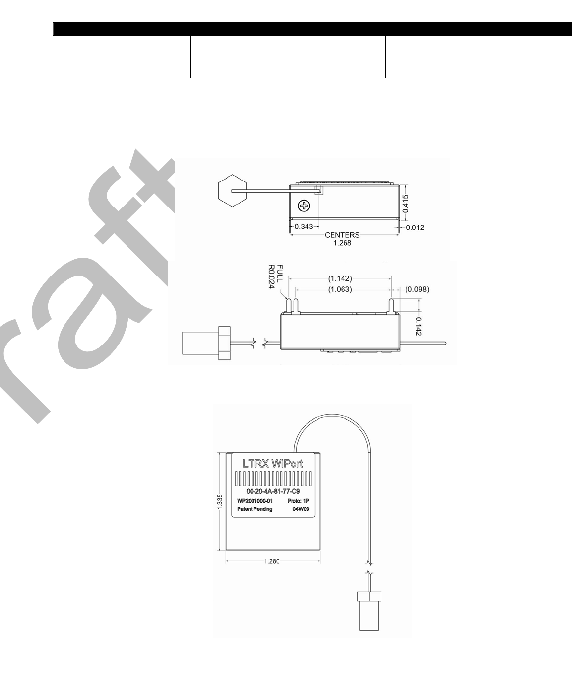
Dimensions
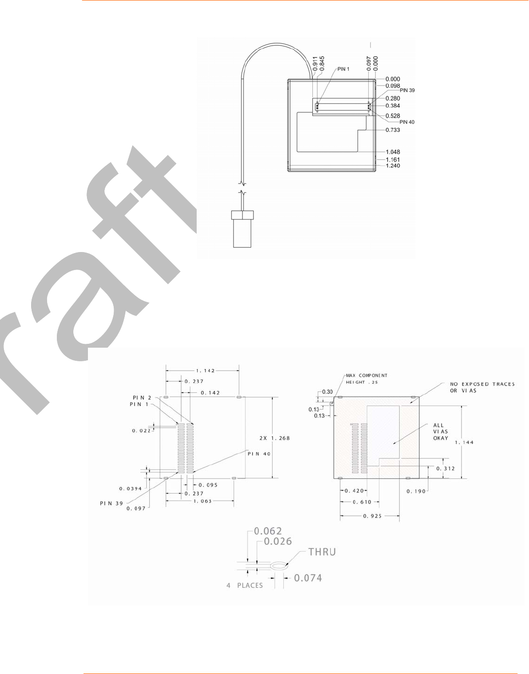
The WiPort dimensions are shown in the following diagrams:
Figure 2-5. Side Views
Figure 2-6. Top View
Description and Specifications
WiPort™ Integration Guide 19
Figure 2-7. Bottom View
Recommended PCB Layout
The hole pattern and mounting dimensions for the WiPort device server are shown in
the following drawing:
Figure 2-8. PCB Layout
Description and Specifications
WiPort™ Integration Guide 20
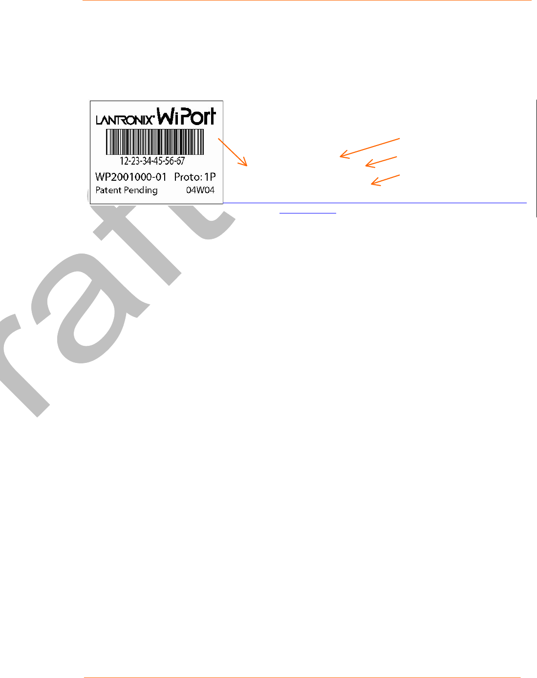
Product Information Label
The product information label contains important information about your specific unit,
such as its product ID (name), bar code, part number, and MAC address.
Figure 2-9. Product Label
The Dashboard must be used to provide an initial configuration before building
an application.
MAC Address
Revision
Manufacturing Code
Part Number

WiPort™ Integration Guide 21
3
3.
.3
3:
:
D
De
ev
ve
el
lo
op
pm
me
en
nt
t
K
Ki
it
t
The WiPort Development Kit includes everything needed to begin to integrate the
WiPort into a given product design.
Contents of the Kit
The development kit contains the following items:
WiPort Evaluation Board
WiPort Device Server
3.3V Power Supply
RS-232 cable, DB9F/F, null modem
CAT5e UTP RJ45M/M Ethernet cable
CD with software utilities and documentation (in PDF format)
Antenna
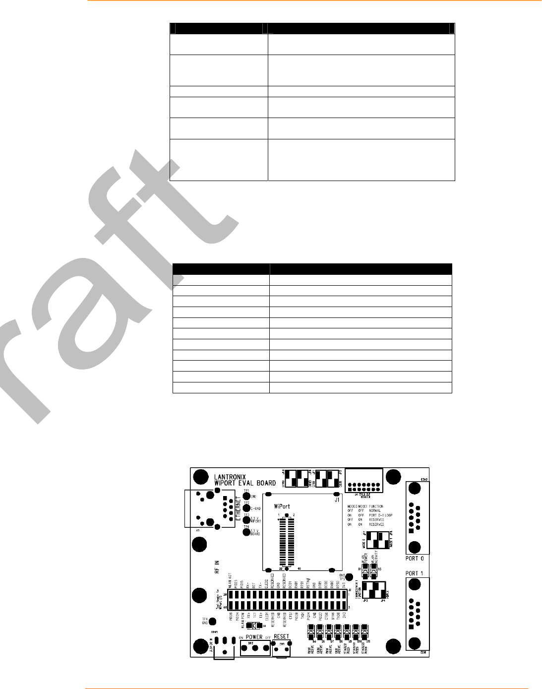
3.1Evaluation Board Description
The WiPort Evaluation Board provides a test platform for the Lantronix WiPort device
server. It supplies 3.3V power. The WiPort Evaluation Board provides access to all
signals to and from the WiPort device server. For connecting to an external device,
the Evaluation Board two serial ports (DTE).
An on-board Complex Programmable Logic Device (CPLD) drives status LEDs and
configures external connections.
Note: Either disregard WLAN POWER and WLAN ACTIVITY LEDs in the
Ethernet Mode or add 15K resistors between test header J2 pin 36 and GND,
and pin 39 and GND. With these resistors, LEDs are OFF in the Ethernet
Mode
Serial Interfaces
The WiPort serial interfaces are 3.3V logic level and typically connected to a
Universal Asynchronous Receiver/Transmitter (UART). For connection to an external
device, the evaluation board has RS-232 and RS-232/422/485 transceivers. Port 0
supports RS-232. Port 1 (channel 2) supports RS-232/485. Connect to a PC using a
null-modem serial cable with 9-pin connectors (F/F).
The table below lists the RS-232 signals and corresponding pins on the WiPort. Note
that the WiPort data and hardware flow control signals are actually buffered by the
evaluation board CPLD. All signals are level-shifted by the RS-232 transceivers.

Development Kit
WiPort™ Integration Guide 22
Table 3-1. RS-232 Signals
WiPort
PIN FUNCTION
DB9
Pin #
UART 0 Con2
TXD0 (Data Out) 3
RXD0 (Data In) 2
CTS0 (HW Flow Control Input) 8
RTS0 (HW Flow Control Output) 7
DCD0 (Modem Control Input) 1
DTR0 (Modem Control Output) 4
UART 1 Con1
TXD1 (Data Out) 3
RXD1 (Data In) 2
CTS1 (HW Flow Control Input) 8
RTS1 (HW Flow Control Output) 7
DCD1 (Modem Control Input) 1
DTR1 (Modem Control Output) 4
Table 3-2. Channel 2 RS-485 4-Wire Connector
WiPort
Signal
Description
DB9 Pin Number
TX+ Data Out 7
TX- Data Out 3
RX+ Data In 2
RX- Data In 8
Table 3-3. Channel 2 RS-485 2-Wire Connector
WiPort
Signal
Description
DB9 Pin Number
TX+/RX+ Data Out/In 7
TX-/RX- Data Out/In 3
Power Supply
The evaluation board uses an external 3.3V regulated supply (included with kit). The
evaluation board contains additional filtering and protection.
General Control PLD
The following table denotes the configuration of the evaluation board. Configuring
the jumper re-routes the signals on the evaluation board as required for a given
product. This also drives the LEDs.
Configuration Switch Bank
Table 3-4. Jumper Configurations
Jumpers Details
JP1 in and JP2 in CP10 and CP4 connected to RS-232
transceiver; can function as DTR1 and
DCD1.
JP1 in and JP2 in
JP1 out and JP2 out
CP10 and CP4 not connected to RS-232
transceiver; can function as general purpose
I/O pins.
Development Kit
WiPort™ Integration Guide 23
Jumpers Details
JP5 in and JP6 in CP2 and CP3 connected to RS-232
transceiver; function as DTR0 and DCD0.
JP5 out and JP6 out CP2 and CP3 not connected to RS-232
transceiver; can function as general purpose
I/O pins.
JP3 in CP0 connected to RS232/RS485 select
JP4 in CP1 connected to RS485 2-wire/4-wire
select
JP7 out and JP8 out WiPort serial ports connected to RS-232
transceivers.
JP7 (Mode 0) In
JP8 (Mode 1) Out
WiPort serial ports not connected to RS-232
transceivers. WiPort serial ports 0 and 1 are
connected directly to each other through the
PLD. Can be used for loopback tests.
Note: Other JP7, JP8 jumper configurations are not recognized by the CPLD
at this time.
If using CPs for any combination of the above evaluation board configurations,
please use the appropriate CP function selection as shown in the following table:
Table 3-5. Configurable Pin Configurations
Configurable Pin Function
CP0 RS-485 Select
CP1 RS-485 2-Wire (Half Duplex)
CP2 Modem Ctrl Out, Channel 1
CP3 Modem Ctrl In, Channel 1
CP4 Modem Ctrl In, Channel 2
CP5 Serial Status LED Out, Channel 1
CP6 Serial Status LED Out, Channel 2
CP7 Diagnostics LED
CP8 General Purpose Input/Output (GPIO)
CP9 GPIO
CP10 Modem Ctrl Out, Channel 2
Evaluation Board Layout
Figure 3-1. WiPort Evaluation Board Layout
Development Kit
WiPort™ Integration Guide 24
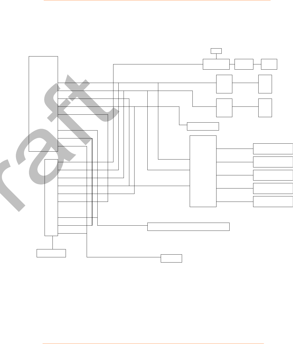
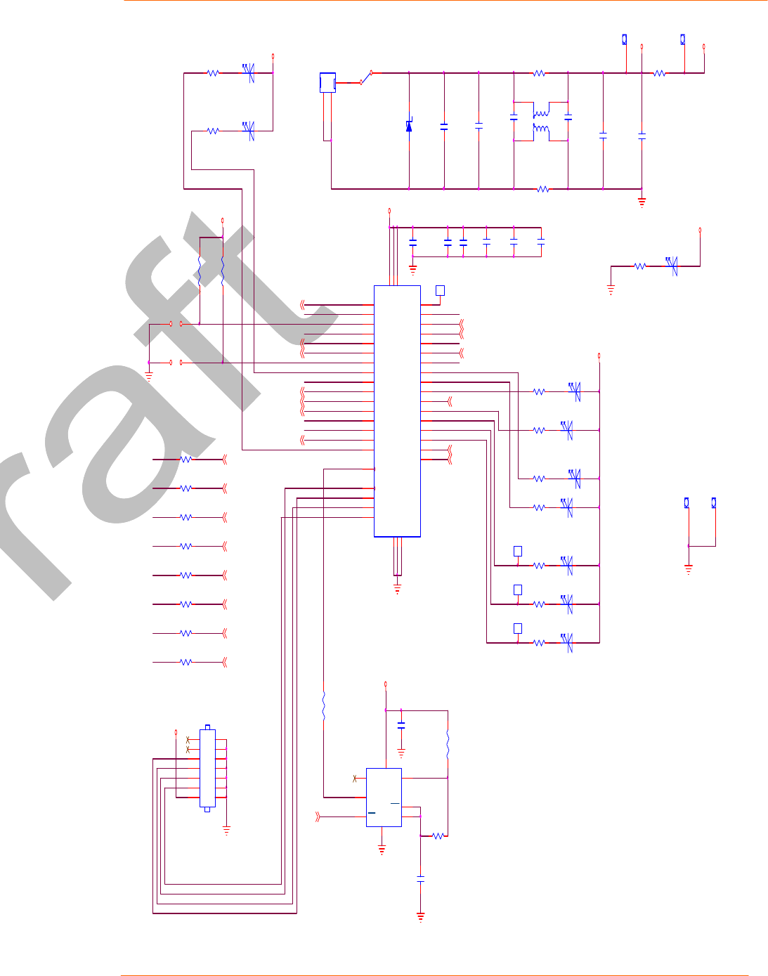
Evaluation Board Schematics
Figure 3-2. Evaluation Board Schematics
RS232
RS232/485
DB9
UART1
TXCVR
3 STATUS LED's
RESET SWITCH
RJ-45 with MAGNETICS and 2 LED's
USB
USB
ANTENNA
PWR
SWITCH
CPLD
RXD1 ACTIVE LED
TXD1 ACTIVE LED
RXD0 ACTIVE LED
TXD0 ACTIVE LED
DB9
TXCVR
LED
PWR
CONN
POWER
SUPPLY
+3.3V
WiPORT
TEST
HEADERS
2X10 - 2EA
I2C/CAN
UART0
UART1
UART0
RESET-
ETH PHY
STATUS LED's
RF LED's
2 LED's
PIGTAIL
I
N
S
T
A
L
L
E
D
W
i
P
O
R
T
I2C/CAN
3.3V
UART0
UART1
RESET-
ETH PHY
STATUS LED's
RF LED's
Development Kit
WiPort™ Integration Guide 25
1
TP1
1
TP2
C3
0.1uF
CP9
C53
0.01uF
C54
0.01uF
2 1
34
SW1
EVO0PFC03M
1
2
C1
4.7uF
RSTIN#
1
2
C4 4.7uF
DNP
DNP
DNP
1
MH3
MHOLE
1
MH2
MHOLE
1
MH4
MHOLE
1
MH 1
MHOLE
C7
0.1uF
CP9
1
2
C5
4.7uF
1
2
C8 4.7uF
WLAN POW
TX-
TCT
WLAN POW
RCT
TX-
TCT
C6
0.1uF
C2
0.1uF
RCT
RX+
CTS0
RX+
CTS0
CTS0
CTS0
RX-
RX-
CP8
CP8
CP3
CP8
CP8
CP3
CP3
CP3
RESERVED
RESERVED
RESERVED
RESERVED
RESERVED
RESERVED
RESERVED
RESERVED
CP10
CP10
RESERVED
CP10
RESERVED
RESERVED
RESERVED
CP10
WLAN POW
WLAN POW
CP7
CP7
RXD0
CP7
1
MH7
MHOLE
2
4
6
8
10
12
14
16
18
20
22
24
26
28
30
32
34
36
38
40
1
3
5
7
9
11
13
15
17
19
21
23
25
27
29
31
33
35
37
39
J1
FTMH12003FDVES
CP7
RXD0
1
MH8
MHOLE
RTS0
RXD1
1
MH9
MHOLE
TXD0
1
MH10
MHOLE
TXD1
RSTIN#
RTS1
2
4
6
8
10
12
14
16
18
20
22
24
26
28
30
32
34
36
38
40
1
3
5
7
9
11
13
15
17
19
21
23
25
27
29
31
33
35
37
39
J2
TSM-120-01-T-DV
RXD0
RXD1
CTS1
RTS0
TXD0
RTS0TXD0
RXD1
RTS1
RTS1
CTS1
TXD1
TXD1
RSTIN#
TXD0 RXD0
ELED1
RESERVED
CTS1
RESERVED
RTS1
RTS0
ELED2
TXD1 RXD1
ELED2ELED1
CTS1
CP1
CP2
CP4
ELED1
RESERVED
RESERVED
CP5
CP0
TX-TX+
CP6
ELED2
TCT
RX+
ELED1
RX-
RCT
CP4
ELED2
CP1
CP0
CP1
CP2
CP5 CP6
CP5
CP0
TX+
CP2
3V3_Wi
CP6
RX+
TX-
CP9
CP4
RCT
TCT
TX+
CP0
RX-
CP6
CP1
CP5
3V3
CP4
CP2
CP9
TX+
WLAN ACT
WLAN ACT
MH7 - MH10 are used
to solder the enclosure
SHIELD
Test Header for WiPort I/O
Place C1,C2, C53 close to J1 pin 1
Place C3,C4, C54 close to J1 pin 2
Wiport Connector
C47
0.1uF
1
2
C48 4.7uF
3V3
C49
0.01uF
1
2
C10 .01uF, HV
1
2
C9
.01uF, HV
3V3
TX+
1
TX-
2
RX+
3
TCT
4
RX-
6RCT
7
NC0
5
NC1
8
LEDRIGHT-
11
LEDLEFT+
9
LEDLEFT-
10
LEDRIGHT+
12
S
H
I
E
L
D
RJ1
RJ2
RJ3
RJ4
RJ5
RJ6
RJ7
RJ8
J3
RJ-45, LU1T041C-43
TX+
TC T
RX+
TX-
RCT
RX-
Ethernet RJ-45
RESET SWITCH
WLAN ACT
R1182
R2182
3V3
ELED1
ELED2
WLAN ACT
1
MH 5
MH OLE
1
MH6
MHOLE
Left LED - ACTIVE (Green)
Right LED - LINK (Yellow)
Development Kit
WiPort™ Integration Guide 26
V
C
C
2
FAST 10
DI/T1IN
16
DE485/T2IN
15
RS485/RS232#
11
Z(B)/T1OUT 5
Y(A)/T2OUT 6
G
N
D
4
B/R1IN 14
A/R2IN 13
R1OUT
7
RO/R2OUT
8
C1-
3
C1+
1
HDPX
12
SHDN# 9
V+
20 V- 17
C2+ 19
C2- 18
RSXXXTTL
U1
MAX3160EAP
5
9
4
8
3
7
2
6
1
1
0
1
1
CON1
DB9-MALE
DCD1_232
DTR1_232
CTS1_B
TXD1_B
RTS1_B
RXD1_B 1234
56
7
8
TS1
ITA25B1
TXD0_232
RXD0_232
CTS0_232
DCD0_232
3V3
G
N
D
1
8
V
C
C
1
9
R1IN 16
R2IN 9
T2I N
12 T1I N
13
C1+
2
C1-
4
V- 7
V+ 3
R1OUT
15
R2OUT
10
T1OUT 17
T2OUT 8
C2+
5
C2-
6
EN-
1
SHUTDOWN-
20
ONLINE-
14
STATUS-
11
RS232
U3
SP3223EUEA
G
N
D
1
8
V
C
C
1
9
R1IN 16
R2IN 9
T2I N
12 T1I N
13
C1+
2
C1-
4
V- 7
V+ 3
R1OUT
15
R2OUT
10
T1OUT 17
T2OUT 8
C2+
5
C2-
6
EN-
1
SHUTDOWN-
20
ONLINE-
14
STATUS-
11
RS232
U2
SP3223EUEA
3V3
RTS1_232/TX+485
RXD1_232/RX+485
TXD1_232/TX-485
DCD1_232
DTR1_232
CTS1_232/RX-485
1
2
C20
0.1uF
1
2
C13 0.1uF
1
2
C18 0.1uF
12
C21
0.1uF
1
2
C30 0.1uF
1
2
C19 0.1uF
1
2
C26 0.1uF
1
2
C31 0.1uF
1
2
C11 0.1uF
1
2
C16
0.1uF
12
C17 0.1uF
12
C14
0.1uF
12
C15
0.1uF
12
C27
0.1uF
12
C28
0.1uF
3V3
3V3
DNP = Do Not Place
Place R4, not R7 to disable slew rate limiting.
Place R7, not R4 to enable slew rate limiting.
1 2
JP3
1 2
JP1
In RS485 mode,
RTS1 is used to
enable the RS485
output driver
R3
10k
1 2
JP2
R8
10k
1 2
JP5
1 2
JP6
1 2
JP4
R5 10k
R6 10k
1
2
C22 .01uF, HV
1
2
C23 .01uF, HV
3V3
3V3
RXD0_B
3V3
DTR0_232
CP2
RXD0_232
RTS0_232
3V3
RTS0_B
CTS0_B
CP3
TXD0_B
TXD0_232
R4
10k
R7
DNP_10k
RS232 PORT 0
RS232 PORT 0/1
RS232/RS485 PORT 1
3V3
CP4
5
9
4
8
3
7
2
6
1
1
0
1
1
CON2
DB9-MALE
1
2
C12 4.7uF
1
2
C25 4.7uF
3V3
CP1
3V3
CP0
CP10
Development Kit
WiPort™ Integration Guide 27
RTS0
TXD1
D4
LN1371-G
R16182
POWER
CTS0_B
3V3
1
2C37
0.1uF, 50V
3V3
RTS0_B
TXD1_B
RTS1_B
RXD0
CTS0
RXD1
CTS1
3V3
C36
100uF, 6.3V, X5R
TXD1_BR
RXD1_B
CTS1_B
1
2C38
0.1uF, 50V
3V3
1
TP3
1
TP4
1
TP5
SW2
1101M2S3CQE2
32
1
CON3
POWER JACK
3V3
3V3
1.5A, 1000 ohms @ 100mHZ
1
2
C40
0.1uF, 50V
C34
22uF, 6.3V, X5R
1
2
D2
1SMB5917BT3, 4.7V
Place CMC1 and remove R9 and R13
to reduce emissions if required.
1
4
2
3
CMC1
DNP_DLW5BSN102SQ2
R9
0
1
2
C32
0.1uF, 50V
1
2
C41
0.1uF, 50V
DC_IN
1
2
C42
0.1uF, 50V
SW2-
TCK
TMS
R13
0
3V3
CPLD ISP HEADER
R28
0
TXD0 ACTIVE
RXD0 ACTIVE
CP5
CP6
CP7
R10
0
R15
10K
D5
LN1371-G
D6
LN1371-G
STATUS1/PIO24
WLAN ACT
STATUS3/PIO26
STATUS2/PIO25
WLAN POW
RXD1_R
1
PAD1
RXD0_R
CTS0_R
1
PAD2
1
PAD3
V
C
C
I
N
T
2
1
G
N
D
1
0
TDO
30
V
C
C
I
N
T
4
1
G
N
D
2
3
I/O0
2
I/O1
3
I/O2
4
I/O32 25
GCK2_I/O3
6
GCK3_I/O4
7
I/O5
8
I/O6
9
I/O16 1
I/O17 44
GTS1_I/O18 42
I/O19 43
GTS2_I/O20 40
GSR_I/O21 39
I/O22 38
I/O23 37
I/O24 36
I/O25 35
I/O26 34
I/O27 33
I/O28 29
I/O8
12
I/O9
13
I/O10
14
I/O11
18
I/O31 26
I/O12
19
I/O13
20
GCK1_I/O
5
TCK
17
TMS
16
TDI
15
I/O7
11
I/O14
22
I/O15
24 I/O30 27
I/O29 28
V
C
C
I
O
3
2
G
N
D
3
1
U4
XC9536XL
SW1-
C44
.01uF
TDI
TDO
C45
.01uF
C46
.01uF
R12182
R1949.9
R17182
R18182
R20182
TXD0_BR
R22182
1
3
5
7
9
2
4
6
8
10
12
14
11
13
J4
CONN PCB 7x2
R23182
R24182
R25182
D9
LN1371-G
D10
LN1371-G
D11
LN1371-G
R14
10K
R2149.9
R2949.9
R3049.9
R3149.9
R3249.9
R3349.9
R3449.9
3V3
TXD0_BR TXD0_B
RTS0_BR
TXD1_BR
RTS1_BR
RXD0_R
CTS0_R
RXD1_R
CTS1_R
RTS0_B
TXD1_B
RTS1_B
RXD0
CTS0
RXD1
CTS1
1
TP6
WLAN POWER
WLAN ACTIVE
D1
LN1371-G
R11182
D3
LN1371-G
RSTIN#
C VOL
5
TRIG 2
THRES 6
G
N
D
1
RST
4
OUT
3
DIS 7
V
+
8
U5
LMC555/SO
1
2
C43
4.7uF
R27 10K
R26
10K
SLOW TIMER
MODE0
MODE1
TXD1 ACTIVE
RXD1 ACTIVE
D7
LN1371-G
D8
LN1371-G
Place C38,C44 close TO U4:21
Place C40,C45 close TO U4:32
Place C41,C46 close TO U4:41
1
2C33
0.1uF, 50V
1 2
JP7
1
2
C35
0.1uF, 50V
RTS1_BR
RTS0_BR
1
PAD4
1 2
JP8
RTS1
CTS1_R
RXD0_B
TXD0_B
3V3_Wi
TXD0

WiPort™ Integration Guide 28
A
A:
:
C
Co
om
mp
pl
li
ia
an
nc
ce
e
a
an
nd
d
W
Wa
ar
rr
ra
an
nt
ty
y
I
In
nf
fo
or
rm
ma
at
ti
io
on
n
Compliance Information
(According to ISO/IEC Guide 22 and EN 45014)
Manufacturer’s Name & Address:
Lantronix 15353 Barranca Parkway, Irvine, CA 92618 USA
Declares that the following product:
Product Name Model: WiPort Embedded Device Server
Conforms to the following standards or other normative documents:
Safety:
UL 60950:2003
CAN/CSA-C22.2 No. 60950:2003
EN 60950:2003 +A1-A4, A11 , Low Voltage Directive (73/23/EEC)
EMC & Radio:
For purposes of certification, the WiPort was tested as a modular device.
CFR Title 47 FCC Part 15, Subpart B and C, Class B
FCC Module Approval
FCC Identifier: R68WIPORTG
Industry Canada ICES-003 Issue 4 (2004), Class B
Industry Canada RSS-Gen Issue 1 (2005)
Industry Canada RSS-210 Issue 6 (2005)
Industry Canada Module Approval IC: 3867A-WIPORTG
EN 301 489-1 v1.4.1 (2002-08) , EMC Directive (1999/5/EC)
EN 301 489-17 v.1.2.1 (2002-08) , EMC Directive (1999/5/EC)
EN 300 328 v1.4.1 (2003-04), R&TTE Directive (1999/5/EC)
Australia / New Zealand AS/NZS CISPR 22 (2006), Class B
Australia / New Zealand AS/NZS 4771 (2000 + A1:2003)
Japan VCCI (EMC emissions) V-3/2006-04
EN55022: 1998 + A1: 2000 + A2: 2003
EN55024: 1998 + A1: 2001 + A2: 2003
EN61000-3-2: 2000 + A2: 2005
EN61000-3-3: 1995 + A1: 2001

WiPort™ Integration Guide
Warranty
Lantronix warrants each Lantronix product to be free from defects in material and
workmanship for a period of TWO YEARS. During this period, if a customer is unable
to resolve a product problem with Lantronix Technical Support, a Return Material
Authorization (RMA) will be issued. Following receipt of a RMA number, the customer
shall return the product to Lantronix, freight prepaid. Upon verification of warranty,
Lantronix will -- at its option -- repair or replace the product and return it to the
customer freight prepaid. If the product is not under warranty, the customer may have
Lantronix repair the unit on a fee basis or return it. No services are handled at the
customer's site under this warranty. This warranty is voided if the customer uses the
product in an unauthorized or improper way, or in an environment for which it was not
designed.
Lantronix warrants the media containing its software product to be free from defects
and warrants that the software will operate substantially according to Lantronix
specifications for a period of 60 DAYS after the date of shipment. The customer will
ship defective media to Lantronix. Lantronix will ship the replacement media to the
customer.
In no event will Lantronix be responsible to the user in contract, in tort (including
negligence), strict liability or otherwise for any special, indirect, incidental or
consequential damage or loss of equipment, plant or power system, cost of capital,
loss of profits or revenues, cost of replacement power, additional expenses in the use
of existing software, hardware, equipment or facilities, or claims against the user by
its employees or customers resulting from the use of the information,
recommendations, descriptions and safety notations supplied by Lantronix. Lantronix
liability is limited (at its election) to:
Refund of buyer's purchase price for such affected products (without
interest).
Repair or replacement of such products, provided that the buyer follows the
above procedures.
There are no understandings, agreements, representations or warranties, expressed
or implied, including warranties of merchantability or fitness for a particular purpose,
other than those specifically set out above or by any existing contract between the
parties. Any such contract states the entire obligation of Lantronix. The contents of
this document shall not become part of or modify any prior or existing agreement,
commitment or relationship.
For details on the Lantronix warranty replacement policy, go to our web site at
www.lantronix.com/support/warranty