File info: application/pdf · 282 pages · 11.78MB
rn~~oo~~~rorr~rn~~ ~w~rr~~ ro~ro~w~~oo
[PDF] oo~~~rorr~rn~~ ~w~rr~~ ro~ro~w - Repeater Builder
... Repeater will be output. Tone A and B frequencies are entered from the ... Z04. = ! TP'Z.07 TP'20S. T. TP201. T. IM4148. B. IO '-l.IR~T i.......:..0--.... .µ ...
Full PDF Document

If the inline viewer fails, it will open the original document in compatibility mode automatically. You can also open the file directly.
Extracted Text
I I
�MOTOROLA
test equipment
, .. ~rn~~oo~~~rorr~rn~~ I ~w~rr~~ ro~ro~w~~oo
R-20018/R-20028
68P81069A93� 0
I '
MOTOROLA INC.
Communications Group
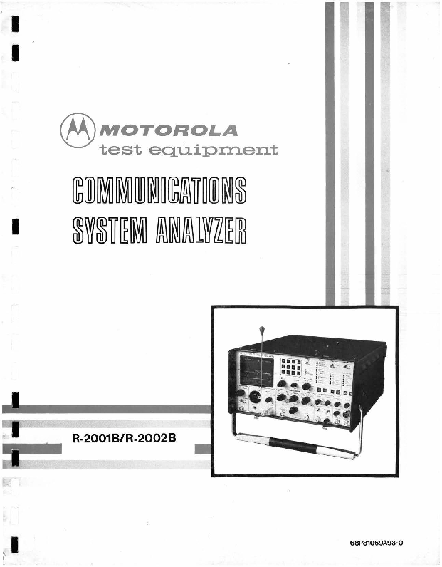
R-2001B/ R-2002B COMMUNICATIONS SYSTEM
ANALYZER
� Motorola, Inc. 1980
All Rights Reserved Printed in U.S.A.
1313 E. Algonquin Road, Schaumburg, II. 60196
68P81069A93-0 6 /30/81-SK
TABLE OF CONTENTS
Paragraph
Page
FOREWORD ............................................................................... 1 SECTION 1
1-1 Introduction .............................................................................. 1-1
SECTION 2 - DESCRIPTION
2-1 2-3 2-4 2-5 2-6 2-7 2-8 2-9 2-10 2-11 2-12 2-13 2-14 2-15 2-16 2-17 2-18 2-19 2-20 2-21 2-22 2-23
Description ............................................................................... 2-1 Microprocessor ........................................................................... 2-1 Display .................................................................................. 2-1 System Warnings ......................................................................... 2-1 Functions ................................................................................ 2-1 AM, FM, CW, DSB Signal Generation ...................................................... 2-2 Simultaneous Modulation ................................................................. 2-2 Modulation Display ....................................................................... 2-2 Sweep Generation ........................................................................ 2-2 SINAD Metering .......................................................................... 2-2 Multi-Mode Code Synthesizer ............................................................. 2,..2 Off-The-Air Monitor ...................................................................... 2-2 IF Display ................................................................................ 2-2 Spectrum Analyzer ....................................................................... 2-3 RF Burnout Protection .................................................................... 2-3 Terminated RF Power Measurement ....................................................... 2-3
I
In-Line Power Measurement. .............................................................. 2-3 Duplex Generator ........................................................................ 2-3 500-kHz Oscilloscope ..................................................................... 2-3 Frequency Counter ....................................................................... 2-4 AC/DC Voltmeter ... �...................................................................... 2-4 Power Supply ............................................................................ 2-4
SECTION 3 - INSTALLATION
3-1 Packing Information ...................................................................... 3-1 3-4 Initial Setup ............................................................................... 3-1 3-5 Analyzer .................................................................... _............. 3-1 3-6 Battery Pack .............................................................�................. "3-2 3-7 Blower Assembly ......................................................................... '3-2
SECTION 4 - OPERATION
4-1 General ...........................................................................:., ...... 4-1 4-3 Controls, Indicators, and Connectors ...................................................... 4-1 4-5 Operation ............................................................................... 4-12 4-7 Calibrate ........ ,-�...................................................................... 4-12
TABLE OF CONTENTS (CONT)
Paragraph
SECTION 4 - OPERATION (CONT)
Page
4-8 4-9 4-10 4-11 4-12 4-13 4-14
Generator Operation ..................................................................... 4-13 Duplex Generation ...................................................................... 4-14 Frequency Counter ...................................................................... 4-15 Spectrum Analyzer ...................................................................... 4-15 Monitor ................................................................................. 4-16 Ext Wattmeter ........................................................................... 4-17 Simultaneous Generate and Measurement Operations ..................................... 4-17
SECTION 5 - MAINTENANCE
5-1 Service ................................................................................... 5-1 5-6 Replacement Parts Ordering .............................................................. 5-1 5-9 Addresses ................................................................................ 5-1 5-10 General Offices ........................................................................... 5-1 5-11 U. S. Orders .............................................................................. 5-2 5-12 Canadian Motorola Electronics Company .................................................. 5-2 5-13 All Countries Except U. S. and Canada .................................................... 5-2 5-14 Major Assemblies ......................................................................... 5-4 5-16 Theory of Operation ...................................................................... 5-7 5-17 General . . . . . . . . . . . . . . . . . . . . . . . . . . . . . . . . . . . . . . . . . . . . . . . . . . . . . . . . . . . . . . . . . . . . . . . . . . . . . . . . . . 5-7 5-20 System Control . . . . . . . . . . . . . . . . . . . . . . . . . . . . . . . . . . . . . . . . . . . . . . . . . . . . . . . . . . . . . . . . . . . . . . . . . . . 5-7 5-25 Generate Mode . . . . . . . . . . . . . . . . . . . . . . . . . . . . . . . . . . . . . . . . . . . . . . � . . . . . . . . . . . . . . . . . . . . . . . . . . . . 5-7 5-34 Power Meter ............................................................................ 5-13 5-40 Monitor Mode ........................................................................... 5-14 5-52 Duplex Generator ....................................................................... 5-16 5-56 Code Synthesizer. . . . . . . . . . . . . . . . . . . . . . . . . . . . . . . . . . . . . . . . . . . . . . . . . . . . . . . . . . . . . . . . . . . . . . . . 5-17 5-65 Frequency Counter ...................................................................... 5-19 5-71 Digital Voltmeter (DVM) .................................................................. 5-19 5-84 Oscilloscope ............................................................................ 5-21 5-96 Sinad Meter ............................................................................. 5-23 5-99 Alignment Procedure .................................................................... 5-24 5-100 Introduction ............................................................................. 5-24 5-102 Test Equipment Required ................................................................ 5-24 5-104 Preparation for Alignment ................................................................ 5-25 5-105 Basic Alignment Procedure .............................................................. 5-25 5-118 Extended Alignment Procedure ........................................................... 5-30 5-126 Checkout Procedure ..................................................................... 5-34 5-127 Introduction ............................................................................. 5-34 5-129 Test Equipment Required ................................................................ 5-34 5-131 Procedure ............................................................................... 5-35 5-146 System Troubleshooting ................................................................. 5-39
SECTION 6 - SYSTEM INTERCONNECT AND PARTS LISTS
ii
TABLE OF CONTENTS (CONT)
Paragraph
Page
SECTION 7 - LOW VOLTAGE POWER SUPPLY (A1)
7-1 7-2 7-6 7-9 7-13 7-14 7-17 7-21 7-24
General .................................................................................. 7-1 Input Power Control ...................................................................... 7-1 DC Output Control ....................................................................... 7-1 Protection Circuitry ....................................................................... 7-1 High Voltage Supply Control ............................................................. 7-2 Switcher Module A1A1 ................................................................... 7-2 Output Module A1A2 ..... �-� ............................................................. 7-2 Control Module A1A3 .................................................................... 7-3 Relay Module A1A4 ...................................................................... 7-4
SECTION 8 - SCOPE AMPLIFIER (A2)
8-1 General .................................................................................. 8-1 8-2 Deflection Amplifiers ..................................................................... 8-1 8-3 Horizontal Timebase Generator ........................................................... 8-1 8-5 Horizontal Switching ...................................................................... 8-1 8-6 Intensity Control ......................................................................... 8-1 8-8 Focus Control ............................................................................ 8-1 8-9 Astigmatism, Geometry, and Trace Rotation ............................................... 8-1
SECTION 9 - SCOPE/DVM CONTROL MODULE (A3)
9-1 9-4 9-7 9-8 9-9 9-11 9-12 9-13 9-17 9-18 9-21 9-22
General .................................................................................. 9-1 Scope Vertical Control .................................................................... 9-1 SSB Detection ............................................................................ 9-1 455 kHz PLL ............................................................................. 9-2 Scope Horizontal Control ................................................................. 9-2 Synthesizer Sweep Control ................................................................ 9-2 Scope Z-Axis Control ..................................................................... 9-2 Modulation Display Control ............................................................... 9-2 Peak Detector ............................................................................ 9-3 DVM Control ............................................................................. 9-3 SINAD Detection ......................................................................... 9-4 Module Control ........................................................................... 9-4
SECTION 10 - RECEIVER (A4)
10-1 General ................................................................................. 10-1 10-2 Down Converter ......................................................................... 10-1 10-4 Linear IF Amplifier and Detectors ......................................................... 10-1 10-8 Audio Switching and Filtering ............................................................ 10-1 10-10 Logarithmic Amplifier and Detector ....................................................... 10-2 10-11 Alarm Generator and Audio Amplifier ..................................................... 10-2 10-12 Module Control. ...........................�.............................................. 10-2
iii
TABLE OF CONTENTS (CONT)
Paragraph
Page
SECTION 11 - RF SYNTHESIZER (AS)
11-1 General ................................................................................. 11-1 11-2 Frequency Synthesis Scheme ............................................................ 11-1 11-5 310-440 MHz Phase Locked Loop ........................................................ 11-1 11-6 60.5 MHz Phase Locked Loop ............................................................ 11-1 11-7 550 MHz Phase Locked Loop ............................................................. 11-1 11-9 500-1000 MHz Phase Locked Loop ....................................................... 11-2 11-10 Modulation Control ....................................................................... 11-2 11-11 Module Control .......................................................................... 11-2
SECTION 12 - AUDIO SYNTHESIZER (A6)
12-1 General ................................................................................. 12-1 12-2 Private Line Generator ................................................................... 12-1 12-7 DPL Generator .......................................................................... 12-1 12-10 1 kHz Tone .............................................................................. 12-2 12-11 External Modulation ..................................................................... 12-2 12-12 Modulation Control ...................................................................... 12-2 12-14 Module Control. ......................................................................... 12-2
SECTION 13 - PROCESSOR 1/0 MODULE (A7}
13-1 General .�................................................................................ 13-1 13-2 10.245 MHz Phase Locked Loop ............................................ :. ..... ;~~~:'.... 13-1 13-3 System Control Bus Interface ................................................. "':-..... .;.. 13-1 ��.� 13-6 DVM ..................................................................................'.. 13-1 13-8 Frequency Counter ...................................................�..... _, ... : ....... '.. 13-1
SECTION 14 - IEEE INTERFACE MODULE (AB}
14-1 14.2 14-3 14-5 14-6
General ................................................................................. 14-1 IEEE Bus Interface ...................................................................... 14-1 RF Level Control ........................................................................ 14-1 Modulation Control ...................................................................... 14-1 Address Decode and Control Latches ..................................................... 14-1
SECTION 15 - PROCESSOR MODULE (A9)
15-1 General ................................................................................. 15-1 15-2 Processor and Buffer .................................................................... 15-1 15-3 Program Memory (ROM) ................................................................ 15-1 15-4 Nonvolatile Memory (NVM) .............................................................. 15-1 15-5 Random Access Memory (RAM) ......................................................... 15-1 15-6 Peripheral Interface Adapter (PIA) ....................................................... 15-1 15-7 Timing Generator ....................................................................... 15-1 15-8 Character Generator .................................................................... 15-1
iv
/
Paragraph
TABLE OF CONTENTS (CONT)
Page
SECTION 1&- HIGH VOLTAGE POWER SUPPLY (A10)
16-1 General ................................................................................. 16-1 16-2 High Voltage Supply ..................................................................... 16-1
SECTION 17 - RF INPUT MODULE (A11)
17-1 General ................................................................................. 17-1 17-2 Input Protection and Power Meter ........................................................ 17-1 17-4 Wideband Amplifier and Frequency Converter ............................................. 17-1 17-9 Duplex Generator ....................................................................... 17-2
SECTION 18 - FRONT PANEL INTERFACE MODULE
18-1 18-2 18-4 18-5 18-6 18-7 18-8
General ................................................................................. 18-1 Input Coupling and Ranging ............................................................. 18-1 DVM Buffer . . . . . . . . . . . . . . . . . . . . . . . . . . . . . . . . . . . . . . . . . . . . . . . . . . . . . . . . . . . . . . . . . . . . . . . . . . . . . 18-1 Frequency Counter Preamp .............................................................. 18-1 Scope Vertical Preamp ................................................................... 18-1 Scope Horizontal Preamp ................................................................ 18-1 Control and Display Interface ............................................................ 18-1
SECTION 19 -10 MHz FREQUENCY STANDARD MODULE (A13)
19-1 General ................................................................................. 19-1
SECTION 20 - FRONT PANEL (A14)
20-1 General. ................................................................................ 20-1 20-2 Display Board ........................................................................... 20-1
SECTION 21 - IEEE - 488 BUS CONTROL
21-1 21-7 21-9 21-10 21-12 21-15 21-24 21-25 21-29 21-30 2f-35 21-36 21-42 21-45 21-46 21-53 21-54
Introduction .......................................................................... 21-1 IEEE-488 Bus Structure ............................................................... 21-3 Bus Signals .......................................................................... 21-3 Data Transfer ........................................................................ 21-3 Programming .......................................................................... 21-3 Command Structure .................................................................. 21-4 Command Strings .................................................................... 21-7 Command Types ..................................................................... 21-7 Trigger Command .................................................................... 21-7 Return Data .......................................................................... 21-7 Programming Commands ............................................................. 21-8 Terminal Mode ....................................................................... 21-8 Error Messages ....................................................................... 21-8 Service Requests ..................................................................... 21-10 Programming Considerations ......................................................... 21-11 General .............................................................................. 21-12 R2002A Analyzer Configuration ....................................................... 21-12
SECTION 22 - BATTERY ASSEMBLY
v
LIST OF ILLUSTRATIONS
Figure
Page
1-1 Communications System Analyzer .......................................................... 1-0 2-1 Accessories Supplied with Analyzer ......................................................... 2-4 3-1 Typical Communication System Analyzer Packaging ......................................... 3-1 4-1 Controls, Indicators, and Connectors, Front Panel ........................................... 4-2 4-2 Controls, Indicators, and Connectors, Left Side Panel ....................................... 4-3 4-3 Controls, Indicators, and Connectors, Rear Panel ............................................ 4-3 4-4 System Analyzer Time Base Calibrate Test Setup and CRT Display .......................... 4-13 4-5 Duplex Generation Test Setup and CRT Display ............................................ 4-14 4-6 Spectrum Test Setup and CRT Display ..................................................... 4-16 4-7 Wattmeter Test Setup and CRT Display .................................................... 4-17 4-8 Test Setup for FM Receiver Sensitivity Using Generator and SINAD
Meter with CRT Display ................................................................... 4-18 4-9 Test Setup for Pager and Alert Functions with CRT Display ................................. 4-19 4-10 Test Setup for Using DVM and Signal Generate with CRT Display ........................... 4-20 5-1 Communication System Analyzer, Top View Cover Removed ................................. 5-6 5-2 Communication System Analyzer, Bottom View Cover Removed .............................. 5-6 5-3 Communication System Analyzer Block Diagram .......................................... 5-9 5-4 Generate Mode Block Diagram ............................................................ 5-12 5-5 Power Meter Block Diagram ............................................................... 5-14 5-6 Monitor Mode Block Diagram ............................................................. 5-15 5-7 Duplex Generator Block Diagram ............................................. -� ........... 5-17 5-8 Code Synthesizer Block Diagram .......................................................... 5-18 5-9 Frequency Counter Block Diagram ........................................................ 5-19 5-10 Digital Voltmeter (DVM) Block Diagram .................................................... 5-20 5-11 Oscilloscope Block Diagram ............................................................... 5-22 5-12 Sinad Meter Block Diagram ............................................................... 5-24 5-13 Scope Amplifier Alignment Points ......................................................... 5-25 5-14 Front Panel Interface Alignment Points ................... : ................................ 5-28 5-15 Scope/DVM Control Alignment Points ..................................................... 5-29 5-16 Horizontal Time Base Alignment Points .................................................... 5-29 5-17 DVM Input Buffer Alignment Points ........................................................ 5-30 5-18 Scope/DVM Control Test Point Numbering ................................................. 5-30 5-19 Processor 1/0 A/D Alignment Points ....................................................... 5-31 5-20 Scope/DVM Control Char Sweep and Sinad Alignment Points ............................... 5-32
vi
LIST OF TABLES
Table
Page
1-1 Physical Characteristics .................................................................... 1-1 1-2 Electrical Characteristics ................................................................... 1-1 1-3 Input/Output Characteristics ............................................................... 1-5 2-1 Accessories Supplied with the Communication Systems Analyzer ............................ 2-5 2-2 Optional Equipment for Use with Analyzer .................................................. 2-5 4-1 Controls, Indicators, and Connectors ....................................................... 4-1 5-1 List of Subassemblies ...................................................................... 5-4 5-2 Control Buses and Functions .............................................................. 5-11 5-3 Basic Test Equipment Required ........................................................... 5-24 5-4 Extended Test Equipment Required ........................................................ 5-25 5-5 Test Equipment ........................................................................... 5-34 5-6 System Troubleshooting .................................................................. 5-39 5-7 Test Point Identification ................................................................... 5-44 7-1 Control Logic Functions .................................................................. 7-3 9-1 Internal DVM Inputs ....................................................................... 9-3
21-1 IEEE-488 Interface Controllable Functions ........................... . 21-2 Command Categories ............................................... . 21-3 Programming Commands ........................................... . 21-4 Terminal Mode ASC II Characters Printable Characters ............... . 21-5 Error Messages ..................................................... . 21-6 SRO Data .......................................................... . 21-7 Code Synthesizer Programming Considerations ...................... .
. ................. 22-2 . ................. 22-4 . ................ 22-5 . ............... 22-9 . ................ 22-10 . ................ 22-10 . ................ 22-11
vii
�
FOREWORD
1. SCOPE OF MANUAL This manual contains information for the installation, operation, and maintenance of the Communications
System Analyzer. 2. PURPOSE AND USE
The Motorola Communications System Analyzer is a portable test instrument, designed specifically for the service and monitoring of communications equipment. Its functions supersede those of a Service Monitor, expanding the features and capabilities to the point wherein servicing is achieved with a single instrument, rather than a host of separate equipmen'i.
The R2001A is the standard Communications System Analyzer. The R2002A Analyzer, which contains the IEEE-488 Standard interface control bus, is also available. Programming for the R2002A is covered in Seeton 21 of this manual.
The Analyzer improves a technician's efficiency and accuracy and reduces servicing time. The Communications System Analyzer performs the functions of signal generation, signal monitoring. and the tests normally associated with the devices listed below.
� Spectrum Analyzer � Duplex Generator � Modulation Oscilloscope � Frequency Counter � AC/DC Digital Voltmeter � RF Wattmeter � General Purpose Oscilloscope � Multi-Mode Code Synthesizer � SINAD Meter � Sweep Generator
The Analyzer meets the shock and vibration requirements of EIA test RS152B, the same specifications met by Motorola mobile radios. This minimizes failures when the instrument is used in a mobile service van, and means it is as tough as the radios it services.
The Communications System Analyzer is designed to be serviced quickly and easily, should a breakdown occur. The majority of the circuitry is on seven modular plug-in circuit boards which have built-in test points that aid in isolating the problem to a specific board. Simple plug-in replacement gets the instrument back in service.
1
CAUTION This equipment contains parts that are subject to damage by static electricity. Proper precautions should be taken during handling.
2
������������
. . . �.'l!~ ~.�
�
� � (:' � s,
�
.,
Figure 1-1. Communications System Analyzer 1-0
SECTION 1
1-1. INTRODUCTION
1-2. This section lists the physical, electrical, and input/output characteristics of the Communications System Analyzer shown in figure 1-1.
Table 1-1. Physical Characteristics
Characteristic
Length Width Height Weight
Description
20.75 inches (52.7 cm) 15.75 inches (40.0 cm)
8.25 inches (21.0 cm) 48 pounds (21.9 kg) (Excluding Battery Pack)
Table 1-2. Electrical Characteristics
Characteristic
Frequency Range Resolution Accuracy
Output (into 50 ohms) Attenuator: Range: Accuracy:
Spectral purity Spurious: Harmonics:
Frequency modulation Range: Accuracy: FM residual noise: External/internal frequency range: External input: Modes:
Description Signal Generator Mode
10 kHz to 999.9999 MHz 100 Hz Equal to master oscillator time base
16 dB variable plus 10 dB steps over 13 ranges 0.1�Vto1 Vrms (-127 dBm to +13 dBm) �2 dB accuracy on 0 dB step attenuator range � 2 dB across other step attenuator ranges � 1 dB over temperature range
~-40 dB ~-15 dB
O - 50 kHz peak �5% of full scale 100 Hz
5 Hz - 10 kHz (�1 dB) Approximately 150 mV for 20 kHz deviation Internal, external, microphone or all simultaneously
1-1
Table 1-2. Electrical Characteristics (Continued)
Characteristic Amplitude modulation
Range: Accuracy: External/internal frequency range: External input: Modes: Double sideband suppressed carrier Carrier suppression:
Frequency Range: Resolution: Accuracy:
Frequency error indicator
Input sensitivity
Spurious response
Deviation Measurement Range: Accuracy: Peak deviation limit alarm:
AM modulation measurement Range: Accuracy:
Description
0 to 80% from 1 to 500 MHz � 10% of full scale from 0% to 50% AM
5 Hz - 10 kHz (�1 dB) Approximately 150 mV for 80%, BNC connector Internal, external, microphone or all simultaneously
~ 25 dB (1 MHz - 500 MHz) Monitor Mode
1 MHz to 999.9999 MHz 100 Hz Equal to that of master oscillator time base
Autoranging CRT display. � 10 Hz resolution for frequency error measurements on 1.5 kHz, 5 kHz and 15 kHz full scale ranges. �1 Hz resolution on the 50 Hz full scale range.
1.5 � V for 10 dB EIA Sinad (narrow band �6 kHz mod. acceptance) 7 � V for 10 dB EIA Sinad (wide
band � 100 kHz mod. acceptance) 4 MHz to 1000 MHz. Useable to 1 MHz.
-40 dB typical 0 dB image at �21.4 MHz -10 dB at LO. harmonics� 10.7 MHz
1, 10, 100 kHz full scale �5% of reading� 100 Hz from 500 Hz to 50 kHz deviation; � 10% of reading from 50 kHz to 75 kHz deviation Set via keyboard to 100 Hz resolution (0 kHz to 99.9 kHz). Audible alarm indicates limit condition in all Monitor Modes.
Oto 100% �5% of full scale
1-2
Table 1-2. Electrical Characteristics (Continued)
Characteristic I
RF Wattmeter (Autoranging display}
Frequency range: Power range: Accuracy: Protection
Dynamic range
Frequency Range Full scale frequency dlspersion:
Frequency offset
Modulation level (FM only}
Size Frequency response External vertical input range Sweep rates Sync
Frequency range
Readout Input sensitivity
Description
1 MHz to 1000 MHz 1.0 watts to 125 wattts � 10%, 1 watt to 125 watts Over temp indicator
General Spectrum Analyzer
~ 75 dB displayed, - 105 dBm to +30 dBm input range with step attenuator
4 MHz to 1;000 MHz Adjustable between 1 MHz and 10 MHz
Duplex Generator
Adjustable from 0 to 10 MHz plus fixed offset of 45 MHz {high or low side) Adjustable from O to 20 kHz peak deviation
Oscilloscope
8 cm x 10 cm DC to 0.5 MHz (3 dB point) 10 mV, 100 mV, 1V, 10V {per division)
1 � s, 10 � s, 0.1 ms, 1 ms, 0.01 S, 0.1 S (per division)
Automatic or normal triggering
Frequency Counter
10 Hz to 35 MHz 5 digit, autoranging 30 mV from 10 Hz to 1 MHz 50 mV from 1 MHz to 35 MHz
1-3
Table 1-2. Electrical Characteristics (Continued)
Characteristic
Readout DC accuracy AC accuracy AC bandwidth
Code Synthesizer Frequency range Resolution Frequency accuracy Distortion Signaling sequences
Tone remote access
Digital private line (DPL) Fixed 1 kHz
Accuracy Distortion External Input Microphone External Jack
Frequency range Level Impedance Code synthesizer external output level
Input level range Sinad accuracy
Digital Voltmeter
Description
Auto ranging digital display, 1, 10, 100, 300 volts full scale. AC-dBm calibrated across 600 ohms. �1% of full scale �1 least significant digit �5% of full scale 50 Hz to 10 kHz
Modulation Source
5 Hz to 9.9999 kHz sinewave 0.1 Hz �0.01% <1% Four fixed
1. Tone only 2. Tone with battery saver 3. Tone and voice 4. Group call Four user programmable Remote base access sequence as follows Tone A for 150 msec Tone B for 40 msec 10 dB below Tone A Tone A continuously 30 dB below the first Tone A burst Codes 000 to 777 and inverted
Equal to master time base <1%
Standard RTM 4000A microphone interface with IDC.
5 Hz to 10 kH:z: 7 vrms maximum 10 Kohm nominal 0-3 vrms into a 600 ohm load
SINAD Meter
0.5V to 10 Vrms �1 dB at 12 dB Sinad
1-4
Table 1-2. Electrical Characteristics (Continued)
Characteristic
Step size Step rate
Standard TCXO
Optional ovenized high stability
AC DC Optional battery Temperature range
Description Manual Frequency Scan
Switch Selectable: 100 Hz, 1 kHz, 10 kHz, 100 kHz and 1 MHz(+ or-) 5 steps/sec.
Time Base
Aging: � 1 x 10⁻⁵ per year Temp: �1 x 10⁻⁵ maximum error over the 0� to 55�C temp. range Agir.J: � 1 x 10⁻⁵ per year Temp: �5 x 10-s maximum error over the 0� to 55�C temp range (warmup to �5 x 10⁻¹ of final frequency within 20 minutes)
Power and Environmental
100-130 VAC, 200-260 VAC 47-63 Hz
+11.5 voe to +16 voe
13.6V battery - provides 1 hour continuous operation
c c 0� to 55� operating; -40 to 85� storage
Table 1-3. Input/Output Characteristics
Characteristic
Input
Description
Ext mod in Mic.
Ext Horiz Vert/Sinad/DVM/Counter In
10K ohms nominal, 150 mV typical for 20 kHz dev. FM or 80% AM Mic input provides bias and IDC limiting suitable for Motorola RTM 9000A handset. PTT switches R2001 from monitor to generate. 1 volt minimum for full screen deflection. Maximum input 10 volts.
1 Meg ohm, 40 pf Nominal; �300 volts DC max, 300 Vrms max at frequencies below 500 Hz, 10 Vrms max up to 35 MHz
� Scope vert in: DC to 500 kHz or SO Hz to 500 kHz AC
mode (�3 dB) � Sinad in: 0.5 to 10 Vrms in at 1 kHz
1-5
Table 1-3. Input/Output Characteristics (Cont)
Characteristics RF In/Out
Ext Wattmeter 10 MHz std in (rear panel)
Description
� DVM in: 1, 10, 100 and 300V full scale AC or DC. AC bandwidth 50 Hz to 10 kHz for �5% F.S. accuracy (AC dBm calibrated across 600 ohms)
� Frequency counter in: 30 mV or greater required from 10 Hz to 1 MHz. 50 mV or greater required from 1 MHz to 35 MHz
50 ohms nominal, 125 watts max (1-1000 MHz}
CAUTION:
The RF In/Out Jack is protected against RF overload. However, to prevent undue stress on the protected circuits it is advisable to always switch the system to the power monitor mode before applying power in excess of 200 mW. Additional protection is also obtained by making it a practice not to leave the step attenuator in the 0 dB position.
Characteristics suitable for Motorola ST-1200 series Wattmeter Elements 70 to 350 mV rms input required at 10 MHz, impedance greater than 50 ohms.
Output
Mod out Demod out
RF in/out Duplex gen out 10 MHz std out (rear panel}
Up to 11 vpp into 600 ohms 10 Hz to 10 kHz Typically 3 vpp into 600 ohms for �5 kHz deviation narrowband, 4 vpp for� 75 kHz deviation wideband. DC to 1O kHz response 1.0 Vrms (+13 dBm) to 0.1 Vrms (-127 dBm) 50 ohm nominal source impedance. 10 kHz to 1.0 GHz. -30 dBm typical, 50 ohm nominal source impedance 2 MHz to 1 GHz
250 mV rms nominal output into 50 ohms
1-6
SECTION 2 DESCRIPTION
L
2-1. DESCRIPTION
r
I
2-2. The Communication System Analyzer is a portable test instrument designed for servicing and
monitoring of portable, mobile, and land base communications equipment operating over the frequency range
of 1 MHz to 1 GHz. The unit performs the functions of signal generation, frequency error and modulation
measurement. It is also capable of a variety of tests normally associated with the following devices:
Spectrum analyzer Duplex offset generator Modulation oscilloscope Frequency counter AC/DC digital-analog voltmeter RF wattmeter General purpose oscilloscope Multi-mode code synthesizer SINAD meter Sweep generator
2-3. MICROPROCESSOR. A Motorola M-6800 series microprocessor permits keyboard entry of data, autoranging of displays, fast frequency access, and permanent storage of often-used frequencies and codes. Generate and monitor RF frequencies, tone codes, and timing sequences can be programmed into a nonvolatile memory, saving time and eliminating entry errors. When one particular type of equipment is continuously serviced, the unit can be programmed to select the mode of operation required when first turned on. 2.4 DISPLAY. All functions, generated or monitored, are presented on an 8 cm x 10 cm cathode ray tube (CRT) in both analog and digital format, with the name of the function being displayed. The CRT also displays control settings eliminating the need for operator search of different equipment panels. Digital readouts are visually aided by the use of the continuously autoranging analog line segments, which are similar to a bar graph. Each has a base line and calibration markers, in addition to the intensified segment showing the measurement. The user selectable displays are listed in a column beneath the DISPLAY heading on the front panel. Choosing a display is accomplished by pressing an arrow button below the column, for up or down movement, as required. When the appropriate arrow is pressed, the LED adjacent to the selected display illuminates. FUNCTION is selected in the same way, providing rapid, accurate changes in service capability at the touch of a button.
2-5. SYSTEM WARNINGS. To aid the technician in servicing, visual warnings will appear on the CRT when certain overload or caution conditions exist. Displays warn of low battery power, overheating of the RF load, or an improper attenuator setting for particular measurements. In addition, a continuous audible alarm sounds when a preset deviation limit is exceeded in monitor modes. This limit is entered by using the keyboard and may be programmed from 0 kHz to 99.9 kHz, with 100 Hz resolution.
2-6. FUNCTIONS. The following paragraphs briefly describe the major functions of the Communications System Analyzer.
2-1
2-7. AM, FM, CW, DSB Signal Generation. The built-in general purpose signal generator provides continuous coverage of the HF, VHF, and UHF land mobile spectrum for receiver testing. Many forms of external and internal modulation can be simultaneously impressed on the carrier signal for actual composite signals. The frequency range of the RF signal generator is from 10 kHz to 1000 MHz in 100 Hz steps. The output of up to 1 Volt rms provides sufficient amplitude to get through misaligned tuners and receivers, and is especially effective when changing a receiver's frequency. The high level, clean output is available over the entire frequency range of the Communications System Analyzer. The output frequency is referenced to an internal time base which can be calibrated to the WWV Standard. (See paragraph 4-7.)
2-8. Simultaneous Modulation. Modulation is simultaneously available from an internal 1 kHz tone
generator, a multi-mode code synthesizer, and from external inputs. The external modulation can be voice
from a standard Motorola mobile radio microphone (which plugs into the front panel of the instrument), as well as a signal applied to the external BNC input. Separate controls are provided for independently setting the
I �~
levels of the 1 kHz tone, the code synthesizer, and the external modulation sources. The 1 kHz test tone is a
convenient source of modulation for making SINAD measurements. A MOD OUT connector provides external
access to all of the modulation signals.
2-9. Modulation Display. The recovered audio waveform, or audio used to modulate the generator carrier, can be viewed on the CRT. It is used to graphically measure deviation, and to aid in waveform analysis.
2-10. Sweep Generation. The sweep generator mode provides an RF output that is swept in frequency across a band centered at the programmed frequency. A synchronized horizontal sweep for the internal oscilloscope allows filter characteristics to be easily determined. This is ideal for in-depth troubleshooting of IF amplifiers and filters.
2-11. SINAD Metering. A comprehensive check of receiver performance can be made with a SINAD measurement. The analog line segment and digital representation of SINAD appear automatically whenever the unit is in the normal generate mode. The only hookups required are from the Communications System Analyzer to the RF input of the receiver under test, and from the audio output of the receiver to the instrument's multipurpose input. The measurement, and appropriate servicing, can then be accomplished without the need for a separate signal generator, SINAD meter or distortion analyzer.
2-12. Multi-Mode Code Synthesizer. The Communications System Analyzer generates Private Line tones (PL), Digital Private Line codes (DPL), two-tone sequential paging codes and tone-remote base signaling tones. All codes are available at the Mod Out jack, as well as being used internally to modulate the RF signal generator. This eliminates the necessity of using separate generators and oscillators for general servicing, setting transmitter deviation, or for checking tone-remote-base control lines. Timing sequences are also stored in the Tone Memory to provide fast set-up and eliminate errors. User programmable timing sequences are also provided to allow the storage of non-standard or future time sequences.
2-13. Off-the-Air Monitor. The 1.5 � V sensitivity of the Communications System Analyzer receiver allows
off-the-air monitoring and measurement of transmitter frequency error and deviation to 1000 MHz. A variable squelch allows weak signals to be monitored, but can be set higher to ensure the proper signal-to-noise ratio for measurement accuracy. The off-the-air monitor function enables frequent parameter checks without leaving the shop, thus spotting system degradation early and keeping service costs down. Bandwidth can be set Wide for off-channel signal location or wide band FM; or Narrow for maximum sensitivity and selectivity.
2-14. IF Display. When the IF display mode is selected, the Communications System Analyzer's receiver IF envelope is shown on the CRT. This allows the technician to qualitatively and quantitatively assess the amplitude modulation envelope of a transmitter.
2-2
2-15. Spectrum Analyzer. In this mode of operation the CRT displays a window of the RF spccti'Um whose bandwidth (from 1 MHz to 10 MHz) is determined by the DISPERSION/SWEEP control. The center frequency of this window ranges from 4 MHz to 1,000 MHz, selectable by entering a specific center frequency with the keyboard. This center frequency is digitally displayed at the top of the CRT screen, eliminating the need for an external signal generator, and counter to provide markers. Once a signal is centered on the screen, positive identification is aided by switching the Analyzer to MONITOR AM or FM and listening to the demodulated output via the built-in audio amplifier and speaker. The spectrum analyzer's center frequency can be scanned up or down at rates varying from 0.5 kHz per second to 5 MHz per second, using the RF scan control. Slow rates are used to precisely determine a subject signal's frequency while faster rates are used for locating intermittent transmissions or viewing large areas of the spectrum in a short time. Uses of the Spectrum Analyzer are: Intermodulation interference identification, IF and RF signal tracing, transmitter harmonics measurements, transmitter spurious checks, and receiver local oscillator radiation.
2-16. RF Burnout Protection. At RF input levels above 200 mW, in any operating mode, the input automatically switches to the internal 125 watt RF load, thus protecting the attenuator and signal generator against damage from a keyed transmitter. If power above 200 mW is applied in any mode except the power monitor mode an audiable alarm sounds and a visual warning on the CRT directs the operator to switch to the power monitor mode.
CAUTION
To prevent undue stress on the protected circuits it is advisable to always switch the system to the power monitor mode before applying power in excess of 200 mW. Additional protection is also obtained by making it a practice not to leave the step attenuator in the 0 dB position.
2-17. Terminated RF Power Measurement. RF power is automatically measured when the Communications System Analyzer is in the Power-Monitor mode. The built-in RF load dissipates up to 50 watts for three minutes and up to 125 watts for one minute. If a high power transmitter should be keyed into the unit for a time long enough to threaten overheating of the power measuring circuitry, the audible alarm sounds and the CRT display changes to read "RF LOAD OVER-TEMP," thus warning the technician to un-key. This instrument function is further enhanced by the simultaneous indication of RF power output, carrier frequency error, and modulation, all on the sarne CRT display.
2-18. In-Line Power Measurement. Use of the Motorola ST-1200 series Wattmeter elements in conjunction with the analyzer's external wattmeter display provides measurement of forward and reflected antenna power on the CRT display. This capability eliminates the complex hook-ups and the additional instruments normally required for antenna measurements.
2-19. Duplex Generator. In this mode, the Communications System Analyzer simultaneously receives and generates the signals for duplex radio servicing, while generated and monitored frequencies are observed on the CRT. In the 0-10 MHz range, the 'Freq. Set' control tunes the proper offset frequency for the VHF and UHF bands. The 45 MHz mode provides a single offset forthe 800 MHz range. A switch is also provided to select high or low side offset, as required. The Duplex Generator provides enhanced capability to service equipment such as repeaters, car telephones and Emergency Medical Telemetry portables.
2-20. 500-kHz Oscilloscope. This general purpose scope is ideal for waveform analysis in two-way communication servicing. Use it for viewing modulation signals (either internally or externally generated), detection of asymmetric modulation or audio distortion, and general purpose signal tracing and troubleshooting.
2-3
2-21. Frequency Counter. The frequency counter measures inputs in a range from 10 Hz to 35 MHz. Its 5 digit auto-ranging output is displayed on the CRT and allows precise measurement and setting of offset oscillators, 35 kHz and 455 kHz pager IF's, PL frequencies and other external input signals. This function will also operate simultaneously with the generate or monitor receiver modes of operation. Frequency measu rement of transm itted carriers and other signals higher than 35 MHz is easily accomplished with the frequ ency error readout in the monitor modes.
2-22. AC/ DC Voltmeter. Switching to the DVM mode provides a digital-analog voltage presentation on the CRT, al ong with the corresponding dBm value. The auto-ranging display provides full scale deflecti ons of 1, 10, 100 and 300 Volts . AC or DC measurement is selected on the CRT . The meter's wide dynam ic ra nge and three digit display are ideal for setting power supply voltages, checking bias levels, and setting audio levels. Like the Frequency Counter, the DVM will operate simultaneously with generate or monitor operation .
2-23. Power Supply. The Communications System Analyzer may be powered by a variety of sou rces:
� AC at 110 or 220 Volts, 50/ 60 Hz � DC from an exte rnal 12 Volt source such as a service vehicle � DC from an optional battery pack. Servicing can thus be accomplished wherever the equipment under
test is located
2-24. A CCESSOR IES.
2-25 . Table 2-1 lists the accessories suppl ied with the Communication System Analyzer. Optional equipment available for use with the unit is listed in Table 2-2 .
SUNSHADE
ACCESSORY KIT
~~.
OSCILLOSCOPE PROBE
ll 1l :
- - - PERFORMANCE REPORT
~..::::::..-=-----.::-:=---
ANTENNA
'
-
IH-1.INE WATTMETER ADAPTER
WARRANTY
J RF INPUT ADAPTER ~ u;.:...
Figure 2-1. Accessories Supplied with Analyzer
2-4
Table 2-1. Accessories Supplied with the Communication Systems Analyzer
�Equipment
Motorola Part No.
Use
Front cover
15-80335A70
Front panel and CRT protection, scorage of cables, power cord, and other equipment for on-site servicing.
Sun shade
15-80335A55
Snap over CRT during use in bright sunlight.
Power cord
30-80336A36
Three conductor cord to supply AC power to unit. Also used when charging optional battery pack.
Oscilloscope probe
RTL-4058A
A X1 probe with attachments for general servicing.
In-line wattmeter adapter RTL-4055A
Allows use of Motorola ST-1200 series in-line wattmeter elements for direct measurement and display of forward and reflected transmitted power.
Coax adapter
58-84300A98
Adapts front panel "N" connector to BNC female.
Antenna
TEKA-24A
Plugs into RF in/out connector on front panel with N to BNC adapter. Used for off-the-air transmitter and receiver tests.
Test microphone
RTM-4000A
Used for voice modulation of signals.
Connector kit
RPX-4097A
Consists of connector shell, clamp, and four connector pins. Used to fabricate a mating plug for male de power connector at back of analyzer. Enables user to make a de power cable to interconnect separate power source to analyzer. Pins 1 and 2 are positive, pin 3 is the charging line, pin 4 is ground.
Table 2-2. Optional Equipment for Use with Analyzer
Equipment
Motorola Part No.
Use
IEEE-488 Standard interface bus option
Consult factory for retrofit information.
Enables fully automatic testing with the unit by external control from a computer or programmable controller.
2-5
Table 2-2. Optional Equipment for Use with Analyzer (Cont)
Equipment Battery pack
High-stability oscillator module Protective cover
Motorola Part No. RTP-1002A
RTL-1007A RTL-4056A
Use
13.6 volt battery and charger attaches to back of the unit. Provides one hour of continuous operation. Cannot be used with IEEE-488 or Blower options.
Improves stability of the time base as specified in electrical characteristics section.
Padded fabric type cover to protect unit from excessive field wear.
' '
I
I I I
2-6
SECTION 3 INSTALLATION
3-1. PACKING INFORMATION
~-~. The unit.is packaged in a fiberboard carton and protected by foam pieces as shown in figure3-1. The unit is first packed in a ~a rd board container and then this carton is packed in a second, larger cardboard container,
for further protection. Save the packing container and materials for future use.
Figure 3-1. Typical Communication System Analyzer Packaging 3-3. All accessories supplied with the analyzer are packed in the analyzer cover. 3-4. INITIAL SETUP 3-5. ANALYZER. To set up the Analyzer for use, place the unit on workbench or in mobile repair unit. Remove the front cover by operating the two latches on the bottom of the cover. Lift the cover and slide it to the side to separate the hinges. Remove the power cord (AC or DC) that is stored in the cover. Attach the female connector of the power cord to the appropriate connector on the rear panel of the analyzer, and the other end to the power source. For AC power a grounded 3 wire power source of 100-130 Vac or 200-260 Vac, 47-63 Hz must be used.
3-1
NOTE The unit is set for 110-130 Vac operation from the factory. For operation from 100110 Vac or 200-260 Vac, the voltage selection card must be readjusted before connection to the power source. This is accomplished by the following procedure:
1. Remove the power cord from the rear panel connector. 2. Slide the selector card cover door over the connector area exposing the selection card and
fuse area. 3. Pull outward on the fuse ejector tab and remove fuse. 4. Remove the printed circuit board voltage selector card by pulling straight to the rear. 5. Reinsert the card at the orientation which causes the appropriate voltage range (marked
on card) to be displayed. 6. Reinstall the fuse. 7. Slide the cover plate back to the original position, connect power cord, and proceed with
system operation. Remove the accessories to be used from the cover. Move the POWER switch to the ON position. When the Oven Ready indicator illuminates the unit's frequency standard is stabilized and the unit is ready for use, (instantaneous with standard TCXO).
CAUTION When installing the analyzer in a vehicle, the DC supply line should be fused close to the vehicle battery. The analyzer is protected against overload by the DC SA fuse on the rear of the unit, but the vehicle is not protected. 3-6. BATTERY PACK. The battery pack is attached to the rear of the analyzer with two clips and two screws. Align and slide the mounting clips of the battery pack into the slots on the mounting brackets on the left side of the back panel of the analyzer. Align the captive screws with the mounting holes on the right of the panel and tighten. Connect the power plug to the connector at the top right of the rear panel.
3-2
SECTION 4 OPERATION
4-1. GENERAL 4-2. This section contains information for the operation of the Communication System Analyzer. 4-3. CONTROLS, INDICATORS, AND CONNECTORS 4-4. The analyzer controls, indicators, and connectors are shown in Figures 4-1 through 4-3 and listed with their functions in Table 4-1.
Table 4-1. Controls, Indicators, and Connectors
Item
Description
Function
Keyboard \J
<l 0 through 9 � Intensity � Focus
Dispr/Sweep control
FRONT PANEL (fig. 4-1)
Twelve-key pushbutton keyboard
Enters variables into memory/enters manual variables/selects variables to be used from the memory.
Line cursor key
Moves the cursor down to the next line that may be changed. Preset permanent entries are skipped. Cursor will move down only. When on last line, will return to top line with next entry.
Horizontal cursor key
Moves the horizontal cursor left to the next entry position that may be changed. When in the last left position, the cursor will move to the far right with the next entry.
Numerical keys
Used to select from the memory a stored value to be used, or to enter directly a value to be used.
Stacked concentric potentiometers
� Intensity - center (small) knob
Controls the intensity of the scope presentation.
� Focus - outside (large) knob
Controls the focus of the scope presentation.
Potentiometer
Controls the frequency span (1-10 MHz) displayed on the CRT when unit is used as a spectrum analyzer. Provides sweep width control when either sweep function (SWP 0.01-1 MHz or SWP 1-10 MHz is selected.
4-1
~
N
79-389t .
-
rm1111 Iii
On
~O�t . . Star' d :>y
.("'' .,,_ ...
� MOQ1,1 ~��o�
� SPf'C! A"��ae�
e ."", ,
\
' p..., ~. ~;It
�! �,
\~/
II II II II II II II II
� 8�11 � �C � OvenA�ady
e� Ol.rr>.e� Ge:'\ ~ruemo' '1' � Ton:e M$1nor-( � Fre<a Co1,ll'lilet � OVM � EKt Wallmetar � IF
� CM . (;W
e� A'-1 ~<,a o�m~��
.etf� '-�
� '''I 1111f1f'lh1lf
,,. � lnn.n'�
� lt'lltlf'l51ly OFocus
,-- �-IE.
- ....
Yof1
eRFtf\f<M;.I
Yof1/Si n a d OVMI Cowt&ef Jn
(?)
�~pr/$-
I ......10
,._
� Yofl OHoht
RF Sc.1n ~Hl/Sect f-1 SK 0 SK (+I
SK
~K
� Sc<;>pc AC � SoopcOC
� $ WPI IO Mll1 � !>WP 01 IM>t1
� All � h��1t�l1..,,wi1t1
5(11(
5(11(
ilM
.W
II m fi1 ii ~M
100'us.c1
100iv
)
MONITOR
SqtletC.h
Volu f"l'WI:
.__/
Codie S1n1h t ...1
' �' ''\""'
0 l~.~.~~�. l [, .re I _.,
Cit
Zeto 8Ml
tAu
l,,...,Opt.
SW
lltogh&
WKle
Mitt t KH' lcvt..
8521-15
Figure 4-1 . Controls, Indicators, and Connectors, Front Panel
_ .........
TIME BASE (FREQ STD) CALIBRATE
8521-18
Figure 4-2. Controls, Indicators, and Connectors, Left Side Panel
e
e
DJ @
�
0
<488 BUS
DJ ~
@
@
AC I.SA
(f)
@
~ e~
Figure 4-3. Controls, Indicators, and Connectors, Rear Panel
4215-18
4-3
Table 4-1. Controls, Indicators, and Connectors (Cont)
Item
Rr: Scan (Hz/Sec) S 1Vitch
Description Eleven position switch
POWER switch
Three-position toggle switch.
Batt indicator AC indicator
LED (red) LED (red)
Oven Ready indicator LED (red)
DISPLAY indicators
Twelve LEDs (red)
Function
Allows automatic scan of the generated or the monitored frequency. The switch setting indicates rate of frequency change. The rate is 5 steps per second, with frequency steps of 100 Hz, 1 kHz, 10 kHz, 100 kHz and 1 MHz.
a. Energizes all circuitry in the On position.
b. At Standby position, removes DC from all circuitry except the frequency standard and battery charger.
c. At Off, only the battery charging circuitry is operative if an ac power source is being used.
Illuminates when equipment is using DC power.
Illuminates when equipment is connected to an ac power source. Position of POWER switch has no effect on indicator. Equipment automatically switches to ac power source when connected to ac line voltage.
Illuminates when optional frequency standard oven has stabilized. Continuously illuminated with the TCXO frequency st~ndard.
Illuminate one at a time to indicate the function or type of operation the equipment is performing and the information displayed on the CRT.
a. Gen/Mon Mtr - In the generate mode the center frequency, output power, and modulation depth of the RF output is displayed. In the monitor mode the center frequency, input power, frequency error, and modulation depth of the received carrier is displayed.
b. Modulation - The modulation audio in the generate mode or the demodulated audio in the monitor mode is displayed.
c. Spect Analyzer - The spectrum analyzer mode is enabled. The RF spectrum and the operating center frequency is displayed.
4-4
Table 4-1. Controls, Indicators, and Connectors (Cont)
Item FUNCTION switch
Description
Three-position toggle switch
Function
d. Duplex Gen - The duplex generate and monitor frequencies are displayed. The depth of modulation on the generator output or on the received carrier is indicated for the generate and monitor modes respectively. For this display, the function switch only selects which modulation reading is displayed.
e. RF Memory - The nine stored RF frequencies or DPL codes with their corresponding PL and the current frequency in use are displayed.
f. Tone Memory - The user selectable parameters for the code synthesizer are displayed. These include the tone A and B frequencies, the signaling sequence, and the programming for each of the eiaht seauences available.
g. Freq Counter - The frequency of the signal input to the front panel frequencv counter jack is displayed.
h. DVM - The AC or DC level of the signal at the front panel DVM jack is displayed. The AC or DC mode is selected with the display cursor and the keyboard. The battery voltage is also displayed.
i. Ext Wattmeter - The external wattmeter element selected and the forward and reflected power being passed thru that element are displayed. The element select is changed by entering the appropriate range number with the kevboard.
j. IF - The 455 kHz IF signal from the monitor receiver is displaved.
k. Scope AC - The voltage waveform applied to the front panel vertical input is displayed. The vertical input is AC coupled.
I. Scope DC - The voltage waveform applied to the front panel vertical input is displayed. The vertical input is DC coupled.
Controls the function of the equipment. The mode is shown by the LEDs.
a. Gen - equipment generates and outputs an RF signal.
4-5
Table 4-1. Controls, Indicators, and Connectors (Cont)
Item
Description
Function
FUNCTION indicators Six LEDs (red)
MODULATION SWITCH
Three position toggle switch
b. Pwr Mon - equipment monitors input signals with the input terminated into the internal power meter. This position must be used for inputs of 0.2 watts and greater.
c. Monitor - equipment monitors input signals with the input terminated into the receive mixer. This position is used for "off the air" monitoring.
Indicates the mode or type of signal the equipment is set up to monitor or generate:
a. FM - equipment generates or monitors frequency modulated signals.
b. CW - equipment generates an unmodulated RF signal. Monitor CW provides frequency error measurement only.
c. AM - equipment generates or monitors amplitude modulated signals.
d. SSB/DSBSC - equipment generates a double sideband suppressed �carrier signal. NOTE: The level of the DSBSC signal generated is not calibrated, it is for use in relative measurements only. Monitor SSB mode receives SSB signals with the use of the BFO.
e. SWP 1-10 MHz - equipment generates a swept RF signal having a sweep width of 1 to 10 MHz, controlled by the Dispr/Sweep control. Selection of Monitor Sweep has no effect, equipment remains in generate mode.
f. SWP 0.01-1 MHz - equipment performs as in e. above except the sweep width limits are 0.01 MHz to 1 MHz.
Controls the Code Synthesizer modulation source. Code Synthesizer mode is shown by the LEDs.
a. Cont - Continuous modulation signal output.
I
nc
I
,t
I
J
3
I
~s
I
4-6
Table 4-1. Controls, Indicators, and Connectors (Cont)
Item
Description
Function
FRONT PANEL (fig. 4-1) (Cont)
CODE SYNTH Mode indicators
Six LEDs (red)
b. Off - Turns off signal. When the mode is DPL or DPL Inv, returning the switch to Off from Cont produces a 133 Hz tone burst for a 120 ms duration.
c. Burst - For PL, tone A, and tone B modes the
I
output is present for as long as the switch is
i
held in the burst position. For the A/B mode
the burst position causes a single signaling
sequence to be output. For the DPL and
DPL Inv modes the Burst position causes a
133 Hz tone to be output. For the Tone
Remote mode either the Burst or the Cont
position causes a tone remote access
sequence to be output. The access sequence
leaves tone A at a low level for transmit-type
commands until the switch is returned to the
Off position. This switch is spring loaded to
return to the Off position from the Burst
position.
When illuminated, indicates the selected mode of the Code Synthesizer.
a. PL/DPL Indicator PL - Selected Private Line frequency output to 1 kHz DPL- Selected Digital Private Line code output Maximum code number is 777.
b. PL/DPL Inv indicator PL - Same as above DPL - Inverted output of selected Digital Private Line code. Maximum code number is 777.
The Private Line frequency or the Digital Private Line code is selected from the RF memory display or entered from the keyboard on the Gen Mon Mtr display.
c. Tone A indicator Indicates Tone A selected for output
d. Tone B indicator Indicates Tone B selected for output
4-7
Table 4-1. Controls, indicators, and Connectors (Cont)
Item
Description
DISPLAY select switches
Two-pushbutton switches
FUNCTION select switches
Two-pushbutton switches
Code Synth Mode select switches
Code Synth Lvl control Ext Level control
Two-push button switches
Potentiometer Potentiometer/switch
Mic connector
4-pin connector
Ext Mod In connector 1 kHz Level control
BNC connector Potentiometer/switch
Function
e. A/B indicator Indicates Tone A/Tone B signaling sequence will be output. See Tone Memor1 Table example, figure 4-9.
f. Tone Remote indicator Indicates access sequence for Motorola Repeater will be output.
Tone A and B frequencies are entered from the keyboard on the Tone Memory Display.
Selects the function to be displayed by the equipment, as indicated by the DISPLAY LEDs.
a. t::,. - moves the selection up one step at a
time
b. \J - moves the selection down one step at
a time
Selects the type or mode of signal the equipment will generate or monitor as indicated by the FUNCTION LEDs. Operation is the same as for the DISPLAY select switches.
Selects the Code Synthesizer output mode as indicated by the CODE SYNTH MODE LEDs. Operation is the same as for the DISPLAY select switches.
Controls the level of Code Synthesizer for modulation or MOD Output.
Controls modulation level of external input (microphone and other external generators). Switch at full counterclockwise position disables external modulation inputs.
Microphone input. Provides microphone bias and PUSH TO TALK (GENERATE) connection to equipment.
External modulation signal input.
Internal 1 kHz tone modulation level control. Switch at full counterclockwise position disables 1 kHz modulation tone.
4-8
Table 4-1. Controls, Indicators, and Connectors (Cont)
Item Mod Out connector
Description BNC connector
Volume control BW switch
Potentiometer Two-position switch
BFO control
Potentiometer/switch
Sig Lvl/Zero Beat indicator
LED (red)
Squelch control
Potentiometer
Image/Dplx switch
Two-position switch
Demod Out connector
Oscilloscope Horiz switch
BNC connector
Seven-position rotary switch
Function
Output connector for all modulation signals (all signals combined).
Controls speaker output level. In either Pwr Mon or Monitor modes selects IF bandwidth. NB is �6 kHz mod acceptance bandwidth. WB is �100 kHz mod acceptance bandwidth. In Gen FM mode selects modulation range. 0-25 kHz dev in NB mode or 0-100 kHz dev in WB mode. BFO on/off and beat frequency control for sideband reception. Full Counterclockwise position is off.
NOTE: To minimize interference the BFO should be turned off when not in use.
Flashes at a rate equal to the difference between the received carrier frequency and the programmed frequency. Also is used as a squelch indicator. Adjusts squelch threshold level, full counterclockwise position disables squelch.
NOTE: Monitor sensitivity is greatly decreased (for high-level use) as the control is increased clockwise beyond the quieting point. In duplex generation mode, controls the duplex frequency output for above (High) or below (Low) the receive programmed frequency. In the monitor mode it selects the frequency of the local oscillator injection above or below the programmed monitor frequency to remove image interference.
Receiver audio output.
When in the oscilloscope mode, selects the horizontal sweep rate or selects the external horizontal input.
4-9
Item
Table 4-1. Controls, Indicators, and Connectors (Cont)
Description
Function
Horiz Vernier control Ext Horiz Trig Level
Position controls �Vert � Horiz
Vert switch
Vert Vernier control Vert/Sinad/DVM/ Counter In connector
Potentiometer
BNC connector Stacked concentric potentiometer and switch
Stacked concentric control led potentiometer Center (small) control knob Outside (large) control knob Four-position rotary switch
Potentiometer
BNC connector
Horizontal sweep rate Vernier or external horizontal input gain Vernier. Calibrated position is fully clockwise.
Allows external horizontal inputs for oscilloscope.
Selects oscilloscope trigger level and trigger mode. Center knob selects the level of trigger. Outside (largest) knob controls the trigger mode. In Auto position, continuous sweep with no vertical input signal, syncs on vertical input. Normal position, no sweep unless vertical input is present, syncs on vertical input.
Controls the position of the CRT display, when in the oscilloscope mode. Controls the vertical position of the CRT display Controls the horizontal position of the CRT display
Oscilloscope operation uses values marked to the right of the switch, indicating volts per division on the CRT. Values marked to the left of the switch are used during modulation display mode, indicating range for calibrated FM deviation.
NOTE: Frequency Counter sensitivity is also controlled by this switch.
Vernier gain control for vertical inputs to the CRT when in the oscilloscope mode. Fully clockwise is the calibrated position.
Signal input to the equipment for the following operations:
a. External vertical for oscilloscope operation
b. SINAD Meter c. Frequency Counter d. Digital Voltmeter
4-10
Table 4-1. Controls, Indicators, and Connectors (Cont)
Item
Description
Function
Type N connector Potentiometer
14-position ganged atten and switch
Ext Wattmeter
Freq Set controls �Coarse �Fine
Frequency offset control (0-10 MHz/Off /45 MHz)
Output connector Frequency Standard control
RF In/out connector
RF input in the power monitor or monitor mode, RF output in the generate mode.
RF Level Variable control
Vernier control of RF output level. Exceeding the AM limit marking in AM generation mode may result in a distorted output.
RF Level Step switch
Ten dB per step control of RF output level in generate mode. Also serves as RF input level step attenuator in monitor and spectrum analyzer modes.
Connector
Allows input from Motorola ST-1200 series inline wattmeter elements for measurement and CRT display of forward and reflected transmitted power.
Stacked concentric potentiometers
Controls the duplex generator output frequency in the Duplex Generation mode.
Inside (small) control r
knob Outside (large) control knob
Coarse frequency control. Fine frequency control.
Three-position switch
Selects the offset of the transmitted frequency from the selected receive frequency (Image/ Dplx switch determines side of selected frequency the offset will be). 0-10 MHz position allows frequency offset to be varied between 0-10 MHz. In the 45 MHz position the offset is variable over a small range around 45 MHz with the use of the Fine frequency control.
BNC connector
Output connector for duplex generator output.
SIDE PANEL (fig. 4-2)
Potentiometer
Allows calibration of the time base frequency (freq std)
REAR PANEL (fig. 4-3)
DC8A
Line fuseholder (8 amp) DC Input line fuseholder
4-11
Table 4-1. Controls, Indicators, and Connectors (Cont)
Item
Description
Function
DC IN power connector AC power connector
4-pin connector 3-pin connector
AC 1.SA 10 MHz std IN connector
Line fuseholder BNC connector
10 MHz std OUT connector
488 BUS connector
BNC connector
Blower power connector
4-pin connector
Connects to DC prime power source
Connects to AC prime power source. Internally patched to accommodate either 100-110 VAC, 110-130 VAC, 200-220 VAC or 220-260 VAC. AC line fuseholder. Provides for external 10 MHz time base input. Equipment automatically switches to external time base with an input at this connector. Provides an output of the internal or external 10 MHz time base for external use. Placement of 1/0 connector when IEEE-488 Interface Bus option is provided. Placement of Blower power connector,
4-5. OPERATION
4-6. The operator may use the CRT display to become familiar with the functions the Communication System Analyzer is capable of performing. The unit may be preset to any of the functions the unit performs. As a function and its parameters are selected they are displayed on the CRT.
The unit contains a nonvolatile memory that stores frequently used data for fast access, reducing setup time. As a function is selected, if data for that function is stored, the data is displayed on the CRT.
One of the stored parameters may be used or the user may manually select (keyboard entry) the parameters required for the function. Selection of stored data or keyboard entry of data is cursor controlled, As a control is changed the CRT display changes to reflect the new parameter being used or function being performed.
4-7. CALIBRATE. The Communication System Analyzer may be calibrated to WWV or other time/frequency standards (figure 4-4). To calibrate the unit's time base (frequency standard) proceed as follows:
a. Connect antenna to RF In/Out connector.
b. Set FUNCTION switch to Monitor and DISPLAY to Gen/Mon Mtr.
c. Enter frequency of time/frequency standards station directly from keyboard.
4-12
d. Select AM function.
e. Using a tuning tool, adjust time base frequency calibration control (on left side of housing) until CRT frequency error display indicates less than 5 Hz error. Frequency settability to 0.5 part per million can thus be achieved using a 10 MHz frequency standard station.
NOTE
The time base output is also available on the rear panel for external measurement or laboratory calibration to better than the 0.5 ppm achievable with the above method
NOTE
An external time base input is also provided on the rear panel.
RF IN/OUT
R-2001A
FUNCTION
ANALOG INDICATOR OF CARRIER ERROR
NEG% AM
] Ii PUT 1,1 fi T T ;
~ :� , ;,
--- ___._____________
- 15.
- : ... ;
. : :..
. : .:� ' ~
1 ,�,,�
100
FREQUENCY
CARRIER ERROR POS % AM
ANALOG INDICATOR OF% AM
8521-22
Figure 4-4. System Analyzer Time Base Calibrate Test Setup and CRT Display
4-8. GENERATOR OPERATION. The system generates RF frequencies for FM, AM, CW, SSB, and DSBSC types of transmission covering a range of 10 kHz to 1000 MHz. To generate a signal the FUNCTION switch is placed in the Gen. position.
NOTE
An RF protection circuit to protect against damage due to inadvertent application of RF power to the unit, when in a generate or sensitive monitor mode, is functional over the full monitor frequency range of the equipment (2 to 1000 MHz).
The type of signal is selected using the FUNCTION select LED indicator column. The unit can deliver an output of up to 1 volt into 50 Ohms. When in the AM generate mode the variable control (located in the RF SECTION on the front panel) should not be set above the AM limit mark. Exceeding this may cause distortion in the output.
4-13
NOTE
The RF protect circuit may trip if generator is run at full power output without having a 50-ohm load connected.
4-9. DUPLEX GENERATION. When operating in the duplex generate mode the offset frequency can be set to either 45 MHz or 0 to 10 MHz (adjustable). The lmage/Dplx switch sets the offset frequency above (high) or below (low) the monitored frequency. When offset is in the 0 to 10 MHz range, the control range may include a fold back region. If the generator is operated in this foldback area erroneous frequency output indications can be given. Avoid areas where backward indication or a jittering display of the offset frequency are incurred. The following is an example of the duplex generator being used to setup repeater levels.
a. Connect DUPLEX GEN output to repeater receiver antenna input and repeater transmitter signal sample to RF In/Out connector. The Duplex Gen Output level is fixed at -30 dBm nominal.
b. Set FUNCTION switch to Gen and DISPLAY to Duplex Gen.
c. Select Duplex Monitor frequency (repeater transmit frequency) from memory table or enter directly from keyboard.
d. Set DUPLEX GENERATOR frequency to repeater receiver frequency.
e. Adjust PL and test tone deviation to desired level on display.
f. Set FUNCTION switch to Monitor and measure the deviation of the repeated signal.
NOTE
Switch function to power monitor and connect repeater transmitter (under 125 watts) directly to the RF In/Out connector to read power and frequency error, as well.
DUPLEX RF OUTPUT IN/OUT
I)
I
RE PEATER RF IN
REPEATER RF OUT
REPEATER
R-2001A
FUNCTION
L' 0 '-E\ MOii ! TOF ~� 4~�E� .E.ooo !'IH:
~I.IPL E). GE~IEF ilTOF 4~�1 .E.OO MH:
REPEATER XMIT FREQUENCY
REPEATED RECEIVED FREQUENCY
NEG DEVIATION OF REPEATED SIGNAL
DEVIATION ALARM - -
s ETTING
-: .u
DIJPLE,, MON
H'./ rHZ
'. ! !:: \.' AL AF 11
POS DEVIATION - - OF REPEATED SIGNAL ~TTE~ �:
8521-27
Figure 4-5. Duplex Generation Test Setup and CRT Display
4-14
4-10. FREQUENCY COUNTER. The frequency counter measures inputs in a range from 10 Hz to 35 MHz. The input to the frequency counter is through the Vert/Sinad/DVM/Counter in, BNC connector (located in the OSCILLOSCOPE section of the front panel). The counter sensitivity is controlled by the scope Vert switch. The following shows the minimum sensitivity for each switch setting:
Switch setting
0.01 0.1 1.0 10.0
- Sen- sitiv-ity
50 mV RMS 500 mV RMS 5V RMS 50V RMS
The autorange output of the counter is displayed on the CRT to a resolution of 0.1 Hz or 5 digits.
NOTE
Do not connect transmitter directly to the frequency counter input. Instead use the RF In/Out connector and the frequency error meter for transmitter frequency measurements.
4-11. SPECTRUM ANALYZER. Input to the spectrum analyzer is through the RF In/Out connector. Select the spectrum analyzer position on the DISPLAY column. Place the FUNCTION switch in the monitor position. Select the desired width of sweep by the Dispr/Sweep control. The center frequency is selected from the memory or entered directly from the keyboard, it is displayed at the top-right of the CRT. The following is an example of locating the frequency of an incoming signal with the spectrum analyzer.
a. Connect antenna to RF IN/OUT connector.
b. Set FUNCTION switch to Mon. and DISPLAY to Spect. Analyzer.
c. Select center frequency from memory table or enter directly from keyboard.
d. Adjust Disp/Sweep control for desired spectrum span.
e. Adjust Step attenuator i,f required to reduce sensitivity.
f. To determine whether a given displayed signal is valid or being internally generated, flip the lmage/Dplx switch to the opposite position. If signal moves in frequency or disappears, it then/represents an internally generated spurious response or received image.
g. Use the RF Scan control to move desired signal to center of the screen. If the signal is located to the right of screen center line, move the RF Scan control clockwise into one of five positive stepping modes. If the signal is to the left of screen center line, turn the RF Scan control counter clockwise to one of five negative stepping modes.
h. Adjust Dispr/sweep control fully counterclockwise for 1 MHz spectrum span.
i. Again use RF Scan to recenter signal on screen.
j. Set DISPLAY to Gen/Mon Mtr.
k. Now adjust the RF scan control to minimize any existing frequency error between the incoming signal and the Monitor frequency.
4-15
I. The frequency indicated at the top of the screen is now that of the desired incoming signal. It can also be monitored for call signs, etc.
NOTE
The spectrum analyzer is functional but uncalibrated for level measurements in Power Monitor mode for tr.ansmitter testing with the built-in 125 watt 50 ohm load. (Observe "RF LOAD OVERTEMP" warning for high power levels or extended periods of use.)
R-2001
CEllTER FREQ
I> 466, nso 111Z .._CENTER
FREQUENCY
� 1 I ..
j
Figure 4-6. Spectrum Test Setup and CRT Display
8521-25
4-12. MONITOR. The analyzer is capable of monitoring the same frequencies that it generates (para 4-9). Select Gen/Mon Mtr in the DISPLAY column and the modulation type in the FUNCTION column. Set the FUNCTION switch to the Monitor position for small signal samples or off the air monitoring. For high power signal monitoring (0.2w to 125w), set the FUNCTION switch to Pwr Mon.
CAUTION
To prevent undue stress on the protected circuits it is advisable to always switch the system to the power monitor mode before applying power in excess of 200 mw. Additional protection is also obtained by making it a practice not to leave the step attenuator in the 0 dB position.
NOTE
High-powereo equipment in the 1-30 MHz range, which has unusually fast carrier rise times, may damage the system analyzer with repeated activation of the protect circuit. Ensure the FUNCTION switch is in the Pwr Mon position (this enables the protect circuit) before RF power is applied to the equipment.
In the monitor mode the CRT displays the type of signal being monitored, the selected frequency, power, error of the received frequency, and the modulation level.
4-16
4-13. EXT WATTMETER. When the analyzer DISPLAY is set to the Ext Wattmeter mode and the Motorola RTL-4055A in-line wattmeter adapter (supplied) is connected to the Ext Wattmeter jack the analyzer measures both forward and reflected power. The power rating of the wattmeter elements (Motorola ST-1200 series*), to be used, are displayed on the CRT. The following is an example of a test setup for external wattmeter operation. Figure 4-7 shows the test set connections and CRT display.
a. Select the EXT Wattmeter function by means of the arrow keys located below the DISPLAY column.
b. Plug the connector of the RTL-4055A In-Line Wattmeter adaptor into the "Ext-Wattmeter" jack located on the RF SECTION of the front panel.
c. Using the keyboard; enter the single digit which corresponds to the full scale power rating of the ST1200 series element you plan to use.
d. Place the ST-1200 element in the In-Line Wattmeter adaptor and install element/adaptor assembly into transmission line.
NOTE
Arrow on In-Line Wattmeter Adaptor must point in the forward direction of the desired rf power flow through the adaptor.
e. Key transmitter and observe magnitudes of forward and reflected power as displayed simultaneously on the 2 analog meter bars and corresponding digital readouts.
EXT WATT METER
I~
R-2001
-
RF TO ANTENNA
~
RF FROM TRANSMITTER
FUNCTION
ANALOG INDICATION OF FORWARD POWER
ANALOG INDICATION OF REFLECTED POWER
~)ti \IAHMETEF
ELEMENT HO I
1) t. 5
2) ~� ;; ' 10
4) ~~.
es:.)~
so
1 Qi)
7) 250
s> soo
~;. 1000
\_. WATT METER ELEMENTS ) TABLE
FYD YATTS
O.O
FORWARD POWER
READING
100
o.c
REFLECTED POWER
READING
!00
8521-12
Figure 4-7. Wattmeter Test Setup and CRT Display
4-14. SIMULTANEOUS GENERATE AND MEASUREMENT OPERATIONS. The following test setups and CRT displays are examples of simultaneous generating and measurement operations.
a. FM Mobile radio setup for receiver sensitivity using Generator and SINAD meter.
1. Connect RF In/Out to mobile radio antenna connector and multipurpose measurement (SINAD) input to receiver audio output.
*Contact your Motorola Parts Source for o"rdering separately.
4-17
2. Set FUNCTION switch to Gen. and DISPLAY switch to Gen/Mon Mtr. 3. Select frequency from RF memory table or enter directly from keyboard. 4. Adjust 1 kHz level for 3.0 kHz deviation and RF level for 12 dB SINAD indication. (The mobile
radio audio output may be set to the desired level using the DVM AC mode.) 5. Read receiver SINAD sensitivity in microvolts or dBm.
RF IN/OUT
0
R-2001
VERT/SINAD DVM/COUNTER IN
I)
�
MOBILE RECEIVER
FUNCTION
ANALOG SINAD INDICATOR NEG DEVIATION
:. :: I':'.< :. � E F11
p~
FF' L[\.'EL
~ :. ,,.
l - ..3 H 11
0
- I0
� 1 (I
8521-23
FREQUENCY DPL CODE
RF OUTPUT LEVEL
DIGITAL SINAD READING
POS DEVIATION ANALOG DEVIATION INDICATOR
Figure 4-8. Test Setup for FM Receiver Sensitivity Using Generator and SINAD Meter with CRT Display
b.' Test pager decode and alert function, and demonstrate simultaneous modulation.
1. Set FUNCTION switch to Gen and DISPLAY to Tone Mem.
2. Select pager frequency from RF memory table or enter directly from keyboard.
3. Enter pager tone code frequencies and select desired time sequence in memory table.
4. Activate and adjust Code Synth. Lvl. for 3.3 kHz deviation on Gen/Mon Mtr. display. (5 kHz system)
NOTE
Timing sequences 1 through 4 are preset and can not be changed. Timing sequences 5 through 8 are keyboard programmable for testing other pager types,
I
upper and lower timing limits, or future schemes.
4-18
RF IN/OUT PAGER
MIKE
R-2001 MIC IN
A TONE
10NE MEMOFY
FREQUENCY - -
SEQ SELECT1 I
B TONE FREQUENCY
PROGRAMMED{ CAN NOT CHANGE
USER TIME { SEQUENCE (MAY BE CHANGED)
~ DLY B DLY
1 ', (1,4(1 0,(10 (1, 0 !.30 TONE
1. � 1..70 0.00 0. O !,;;O E;RT ;.R ..
e. 1.0(1 0.00 3. 0 1,;;0 HH'..'CE
4~ (1,(1(1 0.00
0 3.00 GP-P CL
5� 1.00 O.C5 ;., 0 1.30
~) 7.1 ~)
0.7~� 1.00
0.10
oo..oooo
0.10
'� o!..
0 0 0
!.30 !.30 0.10
TONE ONLY TIME SEQUENCE TONE WITH BATT SAVER TIME TONE AND VOICE TIME SEQUENCE
~ GROUP CALL TIME SEQUENCE
8521-26
Figure 4-9. Test Setup for Pager and Alert Functions with CRT Display
c. Troubleshooting Receiver audio stages using "DVM and Signal Generate" function simultaneously.
1. Select the DVM function by means of the arrow keys located below the DISPLAY column.
2. Using the keyboard "down" arrow position the CRT cursor adjacent to the "DVM Mode" graphics.
3. Enter a "1" via the keyboard to select AC voltage measurement or a "2" for DC voltage measurement selection.
4. Set up the desired on-channel RF signal to provide an input to the receiver.
5. Set Function switch to "Gen". Set appropriate RF output level (as indicated on the CRT screen).
6. Apply test signals from the receiver audio stages to the instrument's "Vert/Sinad DVM/Counter In" input. DC Voltage measurement points are also applied to this same input. The supplied XI test probe may be used.
7. Refer to the CRT screen for an auto-ranging and analog/digital indication of either DC voltage or AC voltage and corresponding dBm level.
NOTE
The AC DVM indication of dBm is referred to 600 ohms.
4-19
I
I
RF IN/OUT 41
I
R-2001
VERT/SINAD DVM/COUNTER IN
0
RADIO UNDER TEST
' TEST PROBE
FUNCTION
ANALOG INDICATION OF DVM READING
!'IQ!; lT OF: Ft1
~) 151,,550 l'IHZ
FREQUENCY
INPUT IJflTTS
(I
- 1 � � I1B11
.
'./ AC
'> D"IM MODE 1) I I FtC DC flE ~� ALAl<:l1 05 .O ~.HZ BAT
o.oo
I 0 .645 .,._ DVM READING
)- DVM SELECT AC OR DC
(I � (I \
~BATTERY
VOLTAGE
8521-24
Figure 4-10. Test Setup for Using DVM and Signal Generate with CRT Display
4-20
SECTION V MAINTENANCE
5-1. SERVICE
5-2. The Motorola Test Equipment Repair Center is charged with the service responsibility for all test equipment supplied by the Motorola Communications Group. The center maintains a stock of original equipment replacement parts and a complete library of service information for all Motorola test equipment.
5-3. Most in-warranty repair are performed at the center. Exceptions include repairs on some equipment not manufactured by Motorola which are performed by the original supplier under the direction of the Test Equipment Repair Center. Out-of-warranty service is performed on a time and materials basis at competitive rates and the maximum turn-around goal is less than ten working days. Customer satisfaction is continually surveyed by reply cards returned with repaired instruments.
5-4. The Test Equipment Repair Center also provides a convenient telephone troubleshooting service. Frequently, a user technician can troubleshoot a piece of equipment and isolate defective components under the direction of the Test Equipment Repair Center via telephone. Required replacement parts are then immediately shipped to the user thereby reducing shipping time and servicing costs. For telephone troubleshooting contact the Test Equipment Repair Center toll free at (800) 323-6967.
5-5. All other inquiries and requests for test equipment calibration and repairs should be directed to the Area Parts Office. They will contact the Test Equipment Repair Center, process the necessary paperwork and, if necessary, have the Center contact you to expedite the repair.
5-6. REPLACEMENT PARTS ORDERING
5-7. Motorola maintains a number of parts offices strategically located throughout the United States. These facilities are staffed to process parts orders, identify part numbers, and otherwise assist in the maintenance and repair of Motorola Communications products.
5-8. Orders for all replacement parts should be sent to the nearest area parts and service center listed below. When ordering replacement parts the complete identification number located on the equipment should be included.
5-9. ADDRESSES
5-10. General Offices
MOTOROLA INC. Communications Division Parts Dept. 1313 E. Algonquin Rd., Schaumburg, Illinois 60196 Phone: 312-397-1000 Executive Offices: 1301 E. Algonquin Rd., Schaumburg, Illinois 60196
5-1
5-11. U.S. Orders
WESTERN AREA PARTS 1170 Chess Drive, Foster City, San Mateo, California 94404 Phone: 415-349-3111 TWX: 910-375-3877
MIDWEST AREA PARTS 1313 E. Algonquin Rd. Schaumburg, Ill. 60196 Phone: 312-576-7322 TWX: 910-693-0869
MID-ATLANTIC AREA PARTS 7230 Parkway Drive Hanover, Maryland 21076 Phone: 301-796-8600 TWX: 710-862-1941
EAST CENTRAL AREA PARTS 12995 Snow Road Parma, Ohio 44130 Phone: 216-267-2210 TWX: 810-421-8845
EASTERN AREA PARTS 85 Harristown Road Glen Rock, New Jersey 07452 Phone: 201-447-4000 TWX: 710-988-5602
PACIFIC SOUTHWESTERN AREA PARTS 9980 Carroll Canyon Road San Diego, California 92131 Phone: 714-578-2222 TWX: 910-335-1634
SOUTHWESTERN AREA PARTS 3320 Belt Line Road Dallas, Texas 75234 Phone: 214-241-2151 TWX: 910-860-5505
GULF STATES AREA PARTS 8550 Katy Freeway Houston, Texas 77024 Phone: 713-932-8955
SOUTHEASTERN AREA PARTS 5096 Panola Industrial Blvd., Decatur, Georgia 30032 Phone: 504-981-9800 TWX: 810-766-0876
5-12. Canadian Orders
CANADIAN MOTOROLA ELECTRONICS COMPANY Parts Department 3125 Steeles Avenue East Willowdale, Ontario Phone: 516-499-1441 TWX: 610-492-2713 Telex: 02-29944LD
5-13. All Countries Except U.S. and Canada
MOTOROLA INC., OR MOTOROLA AMERICAS, INC. International Parts 1313 E. Algonquin Road, Schaumburg, Illinois 60196 U.S.A. Phone: 312-397-1000 TWX: 910-693-1592 or 1599 Telex: 722433 or 722424 Cable: MOTOL
5-2
I
CAUTION This equipment contains parts that are subject to damage by static electricity. Proper precautions should be taken during handling.
I I
5-3
5-14. MAJOR ASSEMBLIES
S-1 S. The Communication System Analyzer is designed for ease of maintenance. Most of the circuitry is on seven plug-in circuit boards. A list of all subassemblies is given in table S-1. The assembly locations are shown in figures S-1 and S-2.
Table S-1. List of Subassemblies
Ref. Des.
Item
Part Number As Labeled
Replacement Order Part No.
A1
Low Voltage Power Supply Module 01-P07897V001
RTP-100SA
A1A1
Low Voltage Power Supply Switcher 01-P07891 V001 Module
RTP-4016A
A1A2
Low Voltage Power Supply Output Module
01-P078S6V001
RTP-4013A
A1A3
Low Voltage Power Supply Control Module
01-P078S3V001
RTP-4012A
A1A4 A2
Lower Voltage Power Supply Relay Module
Scope Amplifier Module
01-P07892V001 01-P00413N002
01-8030SA68 RTC-40078
A3
Scope/DVM Control Module
01-P00409N002
RTC-40088
A4
Receiver Module
01-P00389N002
RTL-10028
AS ASA*
Synthesizer Module Digital Synthesizer Card
01-P0038SN002
RTC-10018
01-P003S8N002
RTC-40098
i
ASB*
RF Synthesizer Card
01-P00386N002
RTC-40108
A6
Audio Synthesizer Module
01-P00426N002
RTC-40118
A7
Processor Input/Output Module
01-P0040SN002
RTC-40128
AB
IEEE Bus Module (Optional)
01-P00203N002
RTC-40138
A9
Microprocessor/Character
Generator Module
01-P07894V001
RTC-40198
S-4
Table 5-1. 'List of Subassemblies (Cont)
Ref.
Part Number
Replacement
Des.
Item
As Labeled
Order Part No.
A10 A11 A11A1* A11A2*
A11A3* A12 A13 A14 A14A1
High Voltage Power Supply Module RF Input Module Protection/Power Meter Card Converter/Wide Band Amplifier Card Offset Generator Card Front Panel Interface Module Frequency Standard Module Front Panel Assembly Display Board Assembly
01-P07896V001 01-P00394N003 01-P00400N002 01-P00398N002
01-P00399N002 01-P07846V001 01-P07898V001 01-P07860V001 01-P07843V001
RTP-1006A RTC-10028 RTL-40618 RTC-40158
RTC-40168 RTL-4086A RTL-1011A 01-80305A64 1-80305A63
Motherboard Assembly
01-P07894V001
RTL-4089A
*These items are solder-in submodules listed for reference purposes. These cards are not normally repaired or replaced individually.
5-5
A1
A9
A8 BRACKET AS SHOWN ON
MODELS V003 AND V004 ONLY
A7
A6 A5 A12 A4 A3 A14
Figure 5-1. Communications System Analyzer, Top View, Cover Removed
A10
A11
A13
Al
81-2376
Figure 5-2. Communications System Analyzer, Bottom View, Cover Removed 5-6
5-16. THEORY OF OPERATION
5-17. General
5-18. The operation of the Communications System Analyzer can be divided into nine basic functions: Generate, Power Meter, Monitor, Duplex Generator, Code Synthesizer, Frequency Counter, Digital Voltme1er (DVM), Oscilloscope, and Sinad Meter. The general operation of the unit will simultaneously incorporate the basic functions to provide the total capability of the system.
5-19. The following discussion will cover the block diagrams for each of the basic functions plus a discussion on the processor control of the system. A functional block diagram of the total system is shown in figure 5-3. Only the major signal paths between each of the modules are shown to clarify the total system configuration.
5-20. System Control
5-21 . System Control is the primary responsibility of the internal microprocessor. Front panel control and system status inputs to the processor are manipulated by the processor to provide the contro l for the operating mode. From the front panel the processor monitors the keyboards, the function select switch , the modulation control switch. the RF scan switch , the image switch , the bandwidth switch, the horizontal and vertical range switches, and the step attenuator switch. This information plus internal status information causes the processor to display the appropriate information on the CRT to program the center frequency, to set up the generate or monitor mode, and to make the internal switching arrangements for the selected operating state.
5-22. The interface to and from the microprocessor is via the processor bus. This bus consists of a 16-bit address bus, an 8-bit data bus, and a 7-bit control bus. This bus interfaces the processor to its program memory (ROM), scratch pad memory (RAM), IEEE interface, and the peripheral interface adapters (PIA). The PIA is the mechanism by which the processor interfaces with the system . A PIA consits of a dual 8-bit latch which may be programmed as either an input or output for the microprocessor. System input and control information passes to and from the microprocessor via three system control buses attached to a PIA.
5-23. Each system control bus consists of a 4 bit address bus, a 4 bit data bus, and an enable line. The 4 address bits determine which of 16 possible latches the 4 bits of data is to be sent to or received from. The enable line triggers the actual transfer of data. The three control buses within the system are called the RF control bus and the AF contro l buses 1 and 2. The RF control bus is as described above while the AF control buses consist of a single 4-bit address and 4-bit data bus and two enable lines. The resulting total input/output capability for the system buses is 16 latches at 4-bits each times 3 buses or 192 bits . A tabulation of buses and the controlling or input function of each bit is shown in table 5-2.
5-24. Systems with the IEEE remote control option interface the IEEE bus to the processor bus through a general purpose interface bus adapter (GPIB ) on the IEEE interface module. When enabled all control inputs to the system pass through the IEEE bus and front panel controls are ignored. For more information on IEEE control see section 21 .
5-25. Generate Mode
5-26. The generate mode provides a variable level RF output that is phase locked to the internal 10 MHz standard. AM, FM , and Sideband Modulation are possible on the output signal. A block diagram of the generate mode is shown in figure 5-4.
I
5-7 /( 5-8 blank)
EXT MOO INPUT MIKE INPUT
EXT 10 MHz IN
IEEE 488 BUS
w(/)
(/)
:c:>c
...J
0a:
Iz -
0
(.;)
w ~
I(/)
>
(/)
RF IN/OUT
EXT FWD PWR
EXT RFL PWR
�
FRONT PANEL INPUTS
-FRONT PANEL OISP
VERT /SINAD/DVM/ FREQ COUNTER IN
EXT HORIZ INPUT
EXT 1 KHz CODE MODULATION AUDIO
A13 10 MHz FREQ STANDARD
-
A6 AUDIO
1� - MOD J> _
LVL
- ...~ 1
_,,
SYNTHESIZER
MOO AUDIO
MOO AUDIO BUS
10 MHz
-
FM MOP_
-
AS RF SYNTHESIZER
RF~
LVL
-
AM AUDIO + DC LEVEL
.-......
-�~ 1
AM AUDIO + DC LEVEL
--
)
0
2i ::>
<(
--
A8 IEEE
z
0 ~ <(
INTERFACE
...J
::>
(OPTIONAL)
�
~
Q w
I-
ac<c(: :::::i
<( (.;)
r--------- - - - - - -- , - SYNTH RF� ~
1 A11 INPUT MODULE
I
-
RF ATIEN CONTROL
I
RF
2
ATIN
-
.
RF
IN/OUT
I
A11A1
-- INPUT PROTECT ANO WATIMETER
DSB MOD RF IN/OUT
-
OPLX MOO
A11A2
WIDEBAND AMPL
ANO DOWN CONVRTER
-
OPLX RFIN
I
RF OUTPUT LVL
A11A3 DUPLEX GENERATOR
I . .
.I 10-7 MHz IF
I
I I
I I I
~ DUPLEX RF
I OUT I
SIDEBAND AUDIO
i I
SPEAKER
CALIBRATED
I
A4 RECEIVER
- OEMOD AUD
SPECTRUM
ANALYZER VERT
-
455 KHz IF
--- - - - - - - - L TEMP
INPUT PWR
I
- ~- -� .J
OVM INPUT BUSS
A3
-
OFFSET FREQ
A12
-EXT OVM
I
I
FRONT PANEL INTERFACE
EXT FREQ
A7 PROCESSOR
1/0
PROCESSOR BUS
IF/BFO FREQ DVM TO AID CONVERTER
SCOPE/OVM CONTROL
A9 PROCESSOR
CHAR. GENZ-AXIS AND SYNC
~
SYSTEM CONTROL BUSES SCOPE VERT FROM ATIENUATOR
INTERNAL SCOPE VERT SCOPE EXT HORIZ
-- EXT 10 MHz OUT MOO OUTPUT
DUPLEX OUTPUT - OEMOO OUTPUT
SCOPE Z-AXIS -
SCOPE VERT
--
SCOPE INT HORIZ
A2 SCOPE
CRT VERT CRT HORIZ
CRT
AMPLIFIER
-
CRT Z-AXIS
1 JUMPERS ARE INSTALLED WHEN THE IEEE OPTION IS NOT INSTALLED.
2 WITH IEEE OPTION. THE RF Attenuator.
IS CONTROLLED FROM THEA8MODULE.
OTHERWISE FRONT PANEL CONTROLLED.
8521-1
Figure 5-3. Communications System Analyzer
Block Diagram
Table 5-2. Control Buses and Functions
~
RF Bus
ADAS D3
D2
D1
DO
AF Bus #1
D3
D2
D1
DO
AF Bus #2
D3
D2
D1
/ DO ADAS
310-440
0 PLL
AO
Audio Synth NO
Display Led's
0
310-440
'
1 PLL
NO
Audio Synth N1
Function Led's
1
310-440
2 PLL
N1
Audi0 Synth N2
Mode Led's
2
60
3 PLL
NO
Audio Synth N3
Input Scope Atten
3
0.001
0.01
0.1
1.0
60
4 PLL
N1
DPL
AUDIO
PL
CLK
DPL
Sy nth
Sel
Enab
Sel
N4
Atten Ext In
Int/Ext AC/DC 4
Sel
Sel
60
5 PLL
N2
MOD
Audio Aduio Audio
To Spkr Atten Atten Atten
RF Atten Position
5
Enab
30 dB 20 dB 10 dB
60
6 PLL
N3
DPLX DSBSC FM
AM
MOD MOD MOD MOD
Scan Switch Position
6
Enab Enab Enab Enab
310-440 7 PLL A1
60 PLL N4
IF Overl'd
SIG
RF Input WB/NB
Present <+20 dB
7
In
In
In
Sw In
500-1000 250-500
B
Out
Out
Enab Enab
WB (MOD) MOD MOD
9 MOD
x (2) INV/INV FM/SWP
Enab
Enab
Sel
Sel
O.Q1- 500-700/ LOOP MOD
A
1000 Sel
700-1000 INV/INV VCO Sel Sel
Disable
DVM MODE Select
CSSG CSSG Hi/Lo Gen
Cont
Burst Image Sw In
B
Sw In Sw In Sw In
Pk Det Pk Det Pk Det FM MOD AM MOD Demod
Enab. Enab Enab
I Scope Vertical Switch Pos In
__
0.1V- 0.01V-
I 10V/ 1V-100kHz 10kHz 1kHz
DIV DIV
DIV
DIV
9
Int DVM x 0.1 WB/NB Sel Enab
IF/BFO Freq Sel
Mon Sw In
Scope Horiz Switch Pos
Sw In
A
B
Horiz Scope
Vert Scope
B
Mode Sel
Mode Sel
c
Pwr MTR
(Mon+ DSB)/ Gen
.01-1
/1-10 Swp
c
Enab
Sel
Sel
SSB
FM
AM Demod
Scope Time Base CTL
D Demod Demod Demod To Spkr
D
Enab Enab Enab Enab
SSC3 SSC2 SSC1 ssco
WB/NB Demod Alarm LIN IF/
E
Sel INV/INV Enab Log IF
Sel
Sel
Scope Time Base CTL SSC7 SSC6 SSC5 SSC4
DVM AC/DC Sel
Freq Cntr Range
E
Ctr/DVM Counter Input Sel
F
Sel
IF/BFO Offset Ext
F
5-11
1 - - - - - - - - - SYS REFF FREQUENCIES
CONTROL
CARRIER �MOD LVL
DSBSC
19
MOD
T/R
STEP ATTEN
INPUT PROTECTION
PROTECTED RF OUTPUT
RCV MXR AND FIRST IF
10 7 IF J5 I
I
8521-44
Figure 5-4. Generate Mode Block Diagram
5-27. The Frequency Standard module (A13) contains a 10 MHz standard oscillator with buffering and switching to provide a 10 MHz signal to the EXTERNAL 10 MHz OUTPUT and to the RF Synthesizer (A5). A provision is made for the application of an EXTERNAL 10 MHz INPUT which causes the internal standard to shut down and the EXTERNAL 10 MHz INPUT to be switched to the EXTERNAL 10 MHz OUT and to the RF Synthesizer.
5-28. The 10 MHz standard input to the RF synthesizer is digitally divided down to provide SYSTEM REFF FREQUENCIES for the frequency counter, the zero beat detector, the second local oscillator in the receiver, and the processor timing reference. Additionally reference frequencies are provided for a fixed 550 MHz locked loop and for a programmable 500 MHz-1000 MHz locked loop. The programming of the 500 MHz-1000 MHz locked loop is provided by the RF CONTROL BUS from the processor. The SELECT SWITCH selects one of three possible output points for the SYNTH RF output signal. The first is from the 500 MHz-1000 MHz loop directly. The second is from a divide by two on the output of the 500 MHz-1000 MHz loop which gives frequencies from 250 MHz to 500 MHz. For outputs below 250 MHz, the output of the 500 MHz-1000 MHz loop is mixed with the fixed 550 MHz signal and the difference signal used for the output. For this output the processor programs the 500 MHz - 1000 MHz loop for frequencies between 550.01 MHz and 800 MHz to obtain outputs from 10 kHz to 250 MHz respectively.
5-29. FM and SWEEP Modulation is implemented within the 500 MHz-1000 MHz loop. FM capability is 200 kHz peak which when divided by two gives the 100 kHz peak requirement. Similarly the sweep capability is 10 MHz peak which provides the 5 MHz requirement for the sweep generator and spectrum analyzer req u i reme,nts.
5-12
5-30. The SYNTH RF signal is amplified and leveled in the RF Input module (A11 ). The signal level at the output of the wideband amp is detected and compared to the AM MOD & DC REF signal from the front panel level control. If there is a difference between the two signal levels, the ALC amp provides an error voltage. The error voltage controls the attenuation of the Voltage Controlled Attenuator (VCA) in the direction that will make the detected RF output equal to the AM MOD & DC REF signal. The;�e are two possible VCA's for the output leveling. The VCA within A11 is used for frequencies from 1 MHz to 1000 Jv1Hz. For frequencies below 1 MHz, the VCA on A 11 is set to minimum attenuation and the VCA on the RF Synthesizer module is used for leveling. Amplitude modulation is incorporated by suming the modulation signal with the DC reference signal to force the leveling loop to vary the output level in proportion to the modulating signal. The signal from the RF level detector (CARRIER+ MOD LVL) is used by the processor for the determination of RF output level and the percent AM. The leveled output range of the Wideband Amp is from -3 dBm to+ 13 dBm (0.16 to 1.0 Vrms).
5-31. The leveled output from the Wideband Amplifier is applied to the Generate/Monitor (T/R) switch. For AM, FM, and CW signals the switch connects the amplifier output to the Step Attenuator. For Double Sideband Suppressed Carrier (DSBSC) the T/R switch is in the "R" position where the amplifier output is connected to the local oscillator port on the receive mixer and the attenuator is connected to the RF port. The DSBSC MOD signal is then used to drive the IF port of the mixer giving a DSBSC signal at the RF port and thus at the Step Attenuator.
5-32. Coarse level control in 10 dB increments is provided by the Step Attenuator. The total range of the attenuator is from 0 dB to 130 dB attenuation. For the basic R2001 A the Step Attenuator is controlled directly by a shaft to the front panel knob. With the IEEE control option the Step Attenuator is electrically programmable and controlled by the processor. The front panel knob in this case is connected only to a rotary switch which directs the processor in setting the attenuation level. Under IEEE control, commands via the IEEE bus determine the attenuator setting. (See section 21.)
5-33. The RF signal from the Step Attenuator passes through the input protection circuitry to the RF Output jack. A level detector on the RF Output jack monitors the power level at the jack. If power in excess of 200 mW is applied to the Output jack, the protection circuit will activate and switch the RF Output jack to the internal 50 ohm load. This action protects the Wideband Amp and Step Attenuator against burnout. A signal line from the protection network signals the processor that the system is in the protected mode. The processor in turn activates the CRT and alarm warnings.
5-34. Power Meter
5-35. Input power measurements are made with the RF Input terminated into an internal 50 ohm load. This termination is the same one used for the protect mode when in the generate or monitor functions. A block diagram of the power meter is shown in figure 5-5.
5-36. For the power meter mode the processor sets the WATT METER ENABLE line to cause the RF input jack to be switched to the 50 ohm power termination. For modes other than the power meter, an Input Detector on the RF Input jack detects when the input power has exceeded 200 mW and then switches the input to the load.
5-37. The switch is a single pole double throw configuration so that when switched to the RF load the path to the Step Attenuator and Converter is open circuited. However, leakage across the open switch provides sufficient signal for operation of the normal monitor functions.
5-13
A11 RF INPUT J1 RF IN-~---...----.t SWITCH
INPUT DET
RF LOAD
STEP ATTEN
SYNTH RF
--=TJE4 =--t
WIDEBAND AMPL
I
10.7 MHz IF
" > - - - - - - - R F INPUT PWR
1-----___.;._..,.~ . OVER TEMP
8521-36
5-38. A sample of the RF voltage being applied to the RF Load is detected by the Power Detector to give a DC output proportional to the peak RF voltage. The amplifier following the detector buffers and gain adjusts the detected voltage to provide the RF INPUT POWER signal to the processor. The processor then determines and displays the RF input power.
5-39. A Temperature Sensor located near the flange of the RF Load alerts the processor when the load temperature exceeds 80� C. The processor reacts to the OVER TEMPERATURE signal by displaying a warning message on the CRT and by sounding the audible alarm.
5-40. Monitor Mode
5-41. The monitor mode allows RF signals from an antenna or from a transmitter directly to be checked for frequency error, modulation level, and spectral content. AM, FM, and sideband modulations can be accommodated with this system. A block diagram of the monitor mode is shown in figure 5-6.
5-42. The RF signal to be monitored is applied to the RF Input jack on the RF Input module (A 11 ). If the input level is less than 200 mW the input signal passes directly through the Input Protection circuitry to the Step Attenuator. For input levels greater than 200 mW the protection circuit switches the input to the internal load and signal the operator to switch to the Power Monitor mode. In this case, RF leakage (paragraph 5-37) through the protection circuits provides the input signal to the Step Attenuator.
5-43. For the monitor mode the T/R switch is set so that the RF input from the Step Attenuator is connected to the RF port on the receive mixer. The output from the wideband amp is switched to the local oscillator port on the receive mixer. The processor programs the RF Synthesizer for an output frequency that is offset from the frequency to be monitored by 10.7 MHz. The offset may be above or below the center frequency as selected by the front panel image switch.
5-14
All RF INPUT
Jl
INPUT
RF INPUT---<..i PROTECTION
A5 RF
SYNTHESIZER
STEP ATTEN
'55 KHz IF
FILTER
FM DE MOD
LOG AMPL ANO OET
I
LI ___ _
ALARM
17
---- 60
---- -91 ------ -D -----
PLL
I
I
c __ _ BFO CONTROL ----'-I"'"4 BFO
PROD DET
DEMODE CAL AUDIO
Figure 5-6. Monitor Mode Block Diagram
5-44. The 10.7 MHz difference signal at the IF port of the receive mixer is amplified and selected by the first IF Amplifier and Filter. The Amplifier provides sufficient gain so that the overall gain of the RF Input module is 10 �2 dB. The IF filter provides a modulation acceptance bandwidth of �100 kHz. The filter output is the 10.7 MHz IF signal to the Receiver module (A4).
5-45. A second mixer in the receiver module down converts the 10.7 MHz IF signal to 455 kHz by mixing the input signal with a 10.245 MHz Second Local Oscillator. The Second Local Oscillator is phase locked to the 1O MHz system standard so that its frequency is as accurate as the standard. The phase locked loop for the Second Local Oscillator is split between two modules. A 10.245 MHz SAMPLE signal is compared with the REFERENCE FREQUENCIES from the RF Synthesizer on the Processor 1/0 module (A7). The comparison provides a TRACKING VOLTAGE error signal to the 10.245 MHz oscillator which corrects its frequency to hold it in lock.
5-46. Immediately following the second mixer is the IF filter. The IF filter is selectable between a narrowband (�6 kHz mod acceptance) and a wideband (�100 kHz mod acceptance) bandwidth. The bandwidth is under the control of the processor and is selected by the bandwidth switch on the front panel.
5-15
5-47. The output signal from the IF filter has two possible paths. The path to the Log Amplifier and Detector provides the spectrum analyzer capability. The other path is the linear IF Amplifier for AM, FM, and SSB demodulation. The output level of the Amplifier is detected to give amplitude modulation and to provide the AGC control on the IF amplifier. The IF signal is applied to the FM Demodulator and is sent to the Scope/DVM Control module (A3) for SSB demodulation and for frequency error determination.
5-48. Demodulated audio from the selected demodulator is routed to the Audio Filter by the Select Switch under processor control. The Audio Filter provides post detection filtering for both wide and narrow band modes. The output of the Audio Filter is three signal lines. The Demod Calibration Audio line provides the calibrated audio levels for modulation level determination. A Demod Audio output provides a level adjusted signal to the front panel Demod Out jack. Speaker audio is level adjusted by the front panel volume control and then amplified by the Audio Amplifier on the Receiver module.
5-49. The Audio Amplifier sums the audio from the demodulator with the Alarm audio. The Audio Amplifier provides a 0.5 watt output capability to the system's internal speaker. The Alarm generator is under the control of the system processor.
5-50. SSB demodulation is implemented on the Scope/DVM Control module by' multiplying the 455 kHz IF signal from !he Receiver with a signal from the Beat Frequency Oscillator (BFO). The BFO is controlled from the front panel and typically has a frequency range of 455 �3 kHz. The BFO signal is switched with the output of the 455 kHz IF Phase Locked Loop (PLL) to the frequency counter for frequency error determination. The455 kHz PLL filters and shapes the IF signal to make it suitable for frequency counting.
5-51. When in the spectrum analyzer mode the linear IF Amplifier is shut down and the Log Amplifier is activated. The output of the Log Amplifier and Detector is a DC voltage that is proportional to the log of the 10.7 MHz IF input level. The log circuit has a dynamic range of approximately 80 dB, covering input levels from -100 dBm to -20 dBm. The SPECTRUM ANALYZER signal from the Log Amplifier is the vertical input to the scope for the spectrum analyzer display.
5-52. Duplex Generator
5-53. Simultaneous generate and monitor functions are available with the use of the Duplex Generator. The frequency spread between generate and monitor frequencies is limited to a range of 0 to 10 MHz and a fixed frequency of 45 MHz. A block diagram of the Duplex Generator function is shown in figure 5-7.
5-54. The Duplex Output signal is generated by mixing the local oscillator signal for the first receive mixer with a signal from the Offset Oscillator. The Offset Oscillator is at the frequency equal to the desired spread between generate and monitor frequencies less the 10.7 MHz IF offset. The monitor function is unaffected by the duplex mode and operates as described under paragraph 5-40.
5-55. Frequency modulation of the duplex output is obtained by modulating the Offset Oscillator frequency via the OFFSET MOD signal line. Control of the Offset Oscillator is directly from the front panel of the system. A OFFSET FREQUENCY output from the oscillator provides an input to the frequency counter for the determination of the duplex frequency.
5-16
RF INPUT
AS
RF
J1
SYNTHESIZER
--------=J1 -i
STEP ATTEN
INPUT PROTECTION
FILTER
I I JS 10.7 MHZ 1--------1~ IF
I
I J6 DUPLEX
- - - - - - - - - - - - - - , - OUTPUT
OCUONPLTERXOL---,,,-----1~
L __
OFFSET MODULATION
-I J7
>--------------~,
OFFSET FREQ
_________ _J
Figure 5-7. Duplex Generator Block Diagram
5-56. Code Synthesizer
5-57. Three simultaneous modulation sources are possible with the internal Code Synthesizer. A private line (PL) or Digital Private Line (DPL) source, a fixed 1 kHz source, and external modulation sources are individually level controllable and sumed together to give the composite modulation audio. The Code Synthesizer provides the modulation source for the system in the generate mode and can be used as an audio frequency source when in the monitor mode. For the IEEE option a provision is made to allow processor control of the modulation levels. A block diagram of the Code Synthesizer is shown in figure 5-8.
5-58. The PL signaling sequence generator is an Audio Synthesizer with an output frequency range from 5 Hz to 10 kHz in 0.1 Hz steps. The frequency is programmed by the processor in response to the operator's request from the keyboard through the CRT display. The Programmable Attenuator following the synthesizer provides 10 dB and 30 dB attenuation levels for the tone remote access sequence.
5-59. DPL Code words are generated by the processor in response to the code entered by the operator. The 23-bit DPL word is stored in the DPL Generator and continuously output when selected. Either PL or DPL signals are switched to the Code Synthesizer Level control on the front panel.
5-60. A 1 kHz reference signal from the RF Synthesizer is bandpass filtered to provide a low distortion 1 kHz sinewave to the front panel 1 kHz Level Control.
5-61. Two sources of external modulation are possible. A standard Motorola microphone interface jack on the front panel and a BNC front panel jack are provided. The microphone input is connected to an IDC circuit for peak limiting. The composite of the two external modulation sources is the signal to the External Level control on the front panel.
5-62. Systems without the IEEE option will have the wipers of the level control pots jumpered to their respective inputs to the summation amp on the Audio Synthesizer module (A6). Those systems with the IEEE option will select on the IEEE Interface module (AB) either the tops of the level controls or their wipers to the Programmable Attenuators for remote or local control respectively. While in the IEEE Control mode the processor controlled Programmable Attenuator on the IEEE module provides the modulation level control. For the local mode the attenuators are programmed for zero attenuation so that the wipers of the level controls set the modulation levels directly.
5-17
I -- A6 AUDIOSYNTHESIZER
I I
AUDIO
I SYNTH
I I
PRGM ATTEN
DPL GEN
1�
I
SEL '26
SW
I CODE SYN TH LVL
I 41
SY NTH 42'
REF
I
(1 KHz)
1 KHz BPFL
I
--
I 46
28
SEL
1 KHz
29
SW
LVL
--
EXT LVL
- 36
30
PRGM ATTEN
PRGM ATTEN
PRGM ATTEN
�
I
I IEEE
l-sus
I�I
I I
42
SEL SW
6
I. SEL
J 3
SW
RF
--------- LVL
PRGM ATTEN_ _
AM MOD+ DC REF
DUPLEX MOD
--
I
DSBSC MOD
Iso
I
MOD CAL AUDIO
I 48 AUDIO SPKR
MOD OUT
8521-41
Figure 5-8. Code Synthesizer Block Diagram
5-63. The three modulation sources are sumed together on the Audio Synthesizer module after the level controls. The composite modulation signal is then switched to the appropriate modulator and applied to the modulation determination circuitry (MOD CAL AUDIO), the audio amplifier (SPKR AUDIO), and the Modulation Output jack (MOD OUT) on the front panel. The signal to the front panel jack is buffered by a Driver Amplifier to provide a low driving source impedance.
5-64. The AM modulation signal at the output of the Select Switch is sumed with a +5 volt signal. This combination provides a DC level to control the average output power of the wideband amp in the RF Input module, and a superimposed modulation signal to give an AM output. The RF Level control on the front panel for local control or the Programmable Attenuator on the IEEE module provide local or remote RF level control by simultaneously attenuating the DC level and the modulating signal. The resulting signal is the AM MOD & DC REFERENCE signal to the RF Input module.
5-18
5-65. Frequency Counter
5-66. Three possible signal sources are made available to the frequency counter for frequency determination. Two of the inputs are from internal system points for the determinations of the offset frequency (OFFSET), and the monitored carrier error frequency (IF/BFO). The third input is the external input (FREQ CNTR INPUT) on the front panel. A block diagram of the frequency counter function is shown in figure 5-9.
A5 RF SYNTH
! -1 A12 FR�N'T PNLiNTE'RF'A-cE___
REF FREQ
f'MPRocEssOOl/O- - - - -- - - - - - ,
1
...,___1_3_4_______6_1!---1~r
I
ATTEN
~ I
-
FREQ 3 CNTR INPUT
- _J
OFFSET - 5-9 I- -
SEL
IF/BFO
SW
FREQ CNTR
--~----------
PIA
'
I
____ _JI
PROCESSOR BUS
CONTROL
A9 PROCESSOR
Figure 5-9. Frequency Counter Block Diagram
8521-39
5-67 .� The external input signal is routed to the Front Panel Interface module (A12). A range Attenuator on the Interface module provides variable sensitivity settings according to the vertical range switch setting on the front panel. An Amplifier following the range Attenuator amplifies and limits the signal amplitude for the frequency counter input.
5-68. A Select Switch on the Processor 1/0 module (A7) routes the desired signal to the Frequency Counter circuitry. The signal selected is controlled by the processor and is determined by the operating mode of the system.
5-69. A 16-bit gated accumulator is used to determine the input frequency. Gate times from 1 msec to 10 sec are automatically selected by the processor to give the maximum possible resolution. The gate times are derived from the RF Synthesizer REFERENCE FREQUENCIES and thus are as accurate as the system time base.
5-70. The 16-bit Frequency Counter output is transferred directly to the processor bus through a Peripheral Interface Adapter (PIA). The processor in turn adjusts the data for the gate time used and then processes the information to obtain the required frequency display.
5-71. Digital Voltmeter (DVM)
5-72. The processor through the DVM circuitry has access to voltage information at a large number of points throughout the system. From this information the processor is able to determine and display parameters such as; output power level, modulation level, input power level and the like. In addition an external voltage applied to the DVM input jack on the front panel can oe measured and displayed for external voltage measurements. A block diagram of the DVM function is shown in figure 5-10.
5-19
fA3SCOPEiiiv'McoNTROL
I MOD
CAL AUDIO _
6_9
-
-
--
<
.
r
i
DEMOD
79 I
CAL AUDIO
+ AND PEAK DET
CARRIER� MOD LVL-'5"9'-+--...,.....,~
LPFL
RF INPUT
PWR
SEL
EXT FWD PWR 55
SW
EXT RFL PWR 571
BATT VOLT
97
0.1 ATTEN
SINAD IN - - - . . i
78
OVER TEMP - - ' - - - - - - - -
I
I
SINAD OUT-----<.i
l _ ___~
DVM INPUT
A12 FRNT PNL INTERFACE ATTEN
rPROCESSOR 0
-::::i
1.0/0.1 ATTEN
I I
ABS VALUE
AID SIGN BIT
I I
PIA
__ J
__ J
6
CONTROL
A9 PROCESSOR
PROCESSOR BUS
8521~
Figure 5-10. Digital Voltmeter (DVM) Block Diagram
5-73. Switching for the DVM input is contained on the Scope/DVM Control module (A3). One of ten internal measurement points may be selected for measurement. The switching action is controlled by the processor and is performed as required to obtain the information on the CRT. To keep the CRT information current, each of the required measurements are made in sequence at an approximate rate of thirty per second. The net effect is a multiplexing of the voltage information to the processor.
5-74. Two modulation signals (MOD CAL AUDIO and CARRIER+ MOD LVL) and a demodulated signal (DEMOD CAL AUDIO) are made available to the peak detectors. Positive and negative peak determination of the selected signal enables the processor to determine the level of modulation.
5-75. A Lowpass Filter (LPFL) removes the DC component from the CARRIER+ MOD LVL signal so that the generate RF output level can be determined. Refer to paragraph 5-30.
5-20
5-76. The RF INPUT POWER and OVERTEMP signal lines from the RF Input module provide the processor inputs for the internal wattmeter. (Paragraph 5-38). External wattmeter element inputs (EXT FWD PWR and EXT RFL PWR) from the front panel jack provide the information for the external wattmeter display.
5-77. A signal line from the DC input jack on the rear panel (BATT VOLT) is brought to the processor for battery voltage determination. The voltage is attenuated by a factor of 10 to stay with the 10 volt maximum input to the select switch. The processor uses the battery voltage measurement to warn the operator when the battery is near it's discharged state.
5-78. Sinad determination utilizes the two remaining inputs to the select switch. For a discussion on the sinad function see para 5-96.
5-79. The selected internal measurement signal is then passed through a range attenuator. Signals from the Select Switch have a 0 to +10 volt range while the DVM input has a 1 volt maximum input requirement. The processor automatically determines and sets the correct range on the attenuator so that the input level to the DVM is maintained at less than 1 volt. For levels from the select switch less than 1 volt, the attenuator is ranged to the unity gain position for maximum measurement resolution.
5-80. A select switch following the internal range attenuator gates either the internal measurement points or the external 'input to the DVM circuitry. External DVM inputs are applied through the front panel jack to the Front Panel Interface module (A12). On the Interface module, a processor controlled switch selects between a direct coupled or a capacitively coupled path for DC and AC measurements respectively. A range attenuator follows the AC/DC switch to provide processor controlled autoranging over a four decade range. Input voltages from 1 millivolt to 300 volt can be handled through the DVM Input.
5-81. For DC measurements a lowpass filter {LPFL) removes AC signal components. The filter provides approximately 25 dB rejection at 50 Hz so that accurate DC measurements can be made with superimposed AC line ripple. When the AC measurement mode is selected the LPFL is reprogrammed for less than 0.5 dB rejection at 10 kHz.
5-82. Positive and negative DVM input levels are full-wave rectified by the Absolute Value circuit on the Processor 1/0 module (A7). The outputs of the Absolute Value circuit provide a positive voltage level equal to the magnitude of the input voltage and a SIGN BIT indicating the polarity of the input signal. For AC measurements a lowpass filter is switched into the Absolute Value circuit to filter the rectified AC input for it's average level. The processor then multiplies by 1.11 to obtain the RMS value.
5-83. An analog to digital converter (A/D) converts the magnitude voltage level into a 10-bit digital word. This digital word when combined with the SIGN BIT is a binary representation of the input voltage level. The peripheral interface adapter transfers the information to the processor.
5-84. Oscilloscope
5-85. Three basic functions are provided for by the system oscilloscope. The alphanumeric and modulation displays provide operating mode and control information for the system. The external oscilloscope feature augments the total system as a general purpose test instrument. A block diagram of the oscilloscope function is shown in figure 5-11.
5-86. Drive signals for the CRT are provided by circuits on the Scope Amplifier module (A2). Horizontal and vertical signals are amplified by their respective amplifiers from 0.5 volt/division input levels to the levels required on the deflection plates. AZ-Axis Modulator circuit controls the cathode to grid bias voltage on the CRT to effect intensity control.
5-21
HORIZ POSITION
A12 FRONT PANEL INTERFACE
EXT 49 HORIZ
AMP
VERT INPUT
V"RT POSITION
4
VERT 5.6 GAIN
SEL SW
24
ATTEN
A9 PROCESSOR
CHAR GEN
45 A2 SCOPE AMPLIFIER
50
43
TIME BASE GEN
16
20
BB
A3 SCOPE/ DVM CONTROL
SWEEP GEN
HORIZ CHAR SWEEP
4
CONTROL
SPECT 27 I
A NA
I
455 91
IF
B7
DEM OD
CAL AUDIO
79
MOD
69
CAL AUDIO
591
CARRIER �MOD LVL
I
VERT CHAR SWEEP
SEL
74
SW
90 60
Z-AXIS
L:=MO_D_
SWEP
8521~
Figure 5-11. Oscilloscope Block Diagram
5-87. The horizontal amplifier input is selected between external and internal scope functions. External functions, Time base Generator or external horizontal input, are switched to a sumation amp where the HORIZONTAL POSITION signal from the front panel is added. The resulting DC offset positions the display horizontally on the CRT.
5-88. Six decade sweep ranges from 1� sec to 100 msec per division are provided by the Time base
Generator. Control of the Time base Generator is from the front panel horizontal switch through the processor. 5-89. Front panel external horizontal inputs are applied to the top of the horizontal vernier gain potentiometer. The wiper of the gain potentiometer is the EXTERNAL HORIZONTAL input signal to the
5-22
preamp on the Front Panel Interface module (A12). The preamp provides the required horizontal input sensitivity and buffers the signal to the select switch on the Scope Amplifier module.
5-90. Internal horizontal signals, Sweep Generator and Character Sweep outputs, are selected on the Scope/DVM Control module (A3). The Sweep Generator provides a sawtooth waveform to the RF Synthesizer module for the sweep generator and spectrum analyzer functions. The sweep signal to the CRT horizontal input causes the scope sweep to be synchronous with the synthesizer sweep for the spectrum and swept filter response displays.
5-91. The Horizontal Character Sweep generator output is a sawtooth waveform that provides the horizontal sweep for the raster scan character display.
5-92. One of four possible vertical signal sources are switched to the Vertical Amplifier input by a Select Switch on the Scope/DVM Control module. The 455 kHz IF and SPECTRUM ANALYZER signals from the Receiver Module provide the IF envelope and spectrum analyzer displays respectively. The Vertical Character Sweep generator gives the vertical sweep for the raster scan character display. The remaining input is the path for external vertical or modulation scope vertical inputs from the Front Panel Interface module.
5-93. A vertical preamplifier on the Interface module gives a vertical sensitivity of 10 millivolt per division and provides positioning and vernier gain capability for its input. The amplifier is preceeded by a four decade range attenuator which is controlled from the front panel vertical switch through the processor. The attenuator provides external vertical input sensitivities from 0.01to1.0 volt per division and modulation scope sensitivities from 0.25 to 25 kHz per division.
5-94. A Select Switch ahead of the Attenuator selects between the external vertical input or the modulation scope inputs. The External Vertical input path is further selected between AC and DC coupling before becoming the vertical input jack on the front panel. The modulation scope signal path is switched to orie of three possible sources on the Scope/DVM Control module. Demodulation signals from the Receiver are selected via the DEMOD CAL AUDIO path, and frequency and amplitude modulation signals via the MOD CAL AUD 10 and CARR IER + MOD LVL signal paths respectively. The Audio Synthesizer module provides the MOD CAL AUDIO signal while the RF Input module gives the CARRIER+ MOD LVL signal.
5-95. AZ-Axis Select circuit on the Scope/DVM Control module gates either the CHARACTER GEN signal for character displays or the retrace blanking signal from the Time Base Generator for scope displays to the ZAxis Modulator on the Scope Amplifier module.
5-96. Sinad Meter
5-97. Sinad, which is defined as the ratio of noise plus distortion to signal plus noise plus distortion, is a measurement of the audio quality at a receiver output. Measurement of the Sinad is implemented with a 1 kHz notch filter. For a receiver receiving a 1 kHz tone the audio output is applied to the 1 kHz notch filter. Sinad is then the ratio of the signal power at the output of the notch filter to the signal power at the input of the notch filter. A block diagram of the Sinad Meter is shown in figure 5-12.
5-98. The Sin ad Input from the front panel is AC coupled to the range Attenuator on the Front Panel Interface module (A 12). Processor control on the Attenuator allows a wide range of input levels to be automatically handled. The output of the Attenuator is routed to the 1 kHz Notch Filter on the Scope/DVM Control module (A3). Detectors, comprised of fullwave rectifiers and filters, on the input and output of the notch filter determine the respective power levels. The DC outputs of the detectors are read by processor through the DVM. The processor determies the ratio between the two readings and displays the Sinad.
5-23
A12 FANT PNL INTERFACE
SINAD IN 3
If-. ATTEN
A3 SCOPE/DVM CONTROL
6 3
-
1 KHz NOTCH FIL
~
DET I----. SINAD OUT
-
DET
~SINADIN
CONTROL
t
I
A9
PROCESSOR
Figure 5-12. Sinad Meter Block Diagram
8521-38
5-99. ALIGNMENT PROCEDURE
5-100. Introduction
5-101. This section provides a basic (para 5-105) and an extended (para 5-118) alignment procedure. The basic procedure requires only the use of a calibrated oscilloscope. It is expected that the basic alignment be performed whenever service work is performed. The extended alignment procedure requires module extenders and a calibrated digital voltmeter in addition to the oscilloscope. The extended procedure should be performed as required after servicing the system. All adjustments not covered in this procedure are to be performed on suitable module test fixtures only.
5-102. Test Equipment Required
5-103. The test equipment or its equivalent listed in table 5-3 is required for the basic procedure. The additional equipment required for the extended procedure is listed in table 5-4.
Table 5-3. Basic Test Equipment Required
Description
Model
*Oscilloscope Test Point Shorting Jumper Nonmetallic Alignment Tool
Motorola R1004A
*An R2001 is a suitable subsitute
5-24
Table 5-4. Extended Test Equipment Required
Description
Model
*Oscilloscope
Motorola R1004A
*Digital Voltmeter
Motorola R1001A
*RF Signal Generator
Motorola R1201A
*Modulation Meter
Boonton 82AD
Receiver Test Cover Extender Card Set
Motorola 15-P01324V001 Motorola 67-P01322V001
*An R2001 is a suitable for use in place of these separate equipments.
5-104. Preparation for Alignment
1. All alignments to be performed at normal ambient temperature.
2. Remove the top cover of the unit to be aligned.
3. Apply power to the unit to be aligned and allow a warmup time of 15 minutes prior to alignment.
5-105. Basic Alignment Procedure
5-106. CRT Astigmatism and Geometry
1. Select the Monitor Function and the Gen/Mon Mtr Display on the R2001 B. Set the Intensity Control for a medium intense display.
2. While using the Focus Control to maintain a focused display at the center of the CRT, adjust the Astigmatism and Geometry potentiometers (Figure 5-13) for the best focus at the outer edges of the CRT while minimizing the pincushion and barrel distortion of the display. The two adjustments are interactive so that repeated small adjustments alternated between the two potentiometers will be required to obtain the best display.
HORIZONTAL HORIZONTAL
VERTICAL
TRACE GEOMETRY ROTATION
Figure 5-13. Scope Amplifier Alignment Points
INTENSITY BALANCE
5-25
5-107. CRT Intensity Bias
1. Select the Scope DC Display and the Ext Horiz. Input mode. Set the Intensity Control fully counter clockwise.
CAUTION
Do not let a dot stay in one place on the CRT screen for more than 30 seconds as a permanent burn in the phosphor will occur.
2. Adjust the Intensity Bias potentiometer (Figure 5-13) until a dot appears on the screen. (The Vertical and Horizontal Position Control on.the front panel may have to be used to bring the dot on to the screen.) Then back off the Intensity Bias potentiometer until the dot just disappears.
5-108. CRT Intensity Balance
1. Select the Scope DC Display and the 1 mSec/Div Horizontal Sweep rate on the R2001 B. Set the Horizontal Timebase Veriner to the Cal position and adjust the Intensity Control for a barely visible horizontal line on the CRT.
2. Adjust the Intensity Balance potentiometer (Figure 5-13) for uniform intensity of the horizontal trace from left to right. The Balance potentiometer affects the intensity on the left side of the trace.
5-109. CRT Horizontal Centering
1. Select the Gen/Mon Mtr Display on the R2001 B.Adjust the Intensity Control for a comfortable viewing brightness.
2. With the Test Point Shorting Jumper connect TP1 of the Scope Amplifier Board (Figure 5-13) to chassis ground.
3. Adjust the Horizontal Position Potentiometer (Figure 5-13) so that the vertical trace on the CRT screen passes through the graticule center point.
4. Remove the jumper from TP1.
5-110. CRT Vertical Centering
1. Select the Gen/Mon Mtr Display on the R2001 B. Adjust the Intensity Control for comfortable viewing brightness.
2. With the Test Point Shorting Jumper connect TP4 of the Scope Amplifier Board (Figure 5-13) to chassis ground.
3. Adjust the Vertical Position Potentiometer (Figure 5-13) so that the horizontal trace on the CRT screen passes through the graticule center point.
4. Remove jumper from TP4.
5-111. CRT Trace Rotation 1. Sel~ct the Gen/Mon Mtr Display on the R2001 B. Adjust the Intensity Control for a comfortable viewing brightness.
2. Adjust the Trace Rotation Potentiometer for a properly rotated CRT display.
5-26
5-112. CRT Horizontal Gain 1. Connect the Mod Out Jack to the Ext Horiz Jack on the R2001 B front panel. 2. Set the R2001 B for the Generate FM Function and the Scope DC Display. Set the Horiz Control for Ext Horiz input. Turn the Code Synthesizer off, the Ext Level off, and the 1 kHz Level up about half way. 3. Connect an oscilloscope with a calibrated vertical input to TP1 on the Scope Amplifier Board. (Figure 5-13). 4. Using therront panel Horizontal Vernier Control adjust for a 3 V p-p amplitude on the sinewave at TP1. 5. With 3V p-p at TP1 adjust the Horizontal Gain Potentiometer (Figure 5-13) for a horizontal trace 6 cm long on the CRT. (Use the front panel controls to position the trace at a convenient place near the center of the CRT).
5-113. CRT Vertical Gain 1. Connect the Mod Out Jack to the Vert Input Jack on the R2001 B front panel. 2. Set the R2001 B for the Generate FM Function and the Scope DC Display. Set the Horiz Control for 1 mSec/Div sweep rate and the Horizontal Vernier to the Cal position. Set the Vert Control for 1 V/Div input sensitivity and the Vertical Vernier to the Cal position. 3. Turn the Code Synthesizer off, the Elt Level off and the 1 kHz Level up about half way. 4. Connect an oscilloscope with a calibrated vertical input to TP4 on the Scope Amplifier Board. (Figure 5-13). 5. Using the front panel 1 kHz Level Control adjust for a 3V p-p amplitude on the sinewave at TP4. 6. With 3V p-p at TP4 adjust the Vertical Gain Potentiometer (Figure 5-13) for a 6cm p-p sinewave on the CRT. (use the front panel Position Controls to center the waveform on the CRT).
5-114. Vertical Input Gain 1. Set the R2001 B for the Generate FM Function and the Scope DC Display. Set the Horiz Control for 1 m Sec/Div sweep rate and the HorizontalWernier to the Cal position. Set the Vert Control for 1 V/Div input sensitivity and the Vertical Vernier to the Cal position. 2. Connect an oscilloscope with a calibrated vertical input to the Mod Out Jack on the front panel. 3. Turn the Code Synthesizer off, the Ext Level off and adjust the 1 kHz Level Control for a 6 V p-p sinewave on the attached oscilloscope. 4. Disconnect the oscilloscope from the Mod Out Jack and connect the Mod Out Jack to the Vert Input Jack on the R2001 B. 5. Adjust the Input Vertical Gain Potentiometer on the Front Panel Interface Board (Figure 5-14) for a 6 cm p-p sinewave on the CRT. (Use the front panel Position Controls to center the waveform on the CRT.)
5-27
K6
K7
KS
l[)
0
DVM ZERO (COARSE)
INPUT VERTICAL GAIN
5-115. DVM Zero 1. Select the DVM Display and the DC Mode on the R2001 B. 2. Short the center conductor of the DVM Input Jack to ground. 3. Adjust the DVM Zero (Coarse) and the DVM Zero (Fine) Potentiometers on the Front Panel Interface Board (Figure 5-14) for a zero reading on the DVM Display.
5-116. Spectrum Analyzer Centering 1. Select the Spect Analyzer Display on the R2001 B.Set the Dispersion Control on the front panel to the 1 MHz position. (full counter clockwise) Set the center frequency of the analyzer to 10.0 MHz. 2. Connect the 10 MHz Output on the rear panel to the RF Input on the front panel. Set the RF Step Attenuator to obtain a convenient spectral display. 3. Adjust the Spectrum Analyzer Centering Potentiometer on the Scope/DVM Control Board (Figure 515) so that the spectral line on the CRT is centered about the center graticule line.
5-117. Horizontal Time Base 1. Select the Tone Memory Display and the Generate FM Function on the R2001 B. Program tone A for 20.0 Hz and Tone B for 2000.0 Hz. 2. Select the Modulation Display. Set the Oscilloscope Controls for 2.5 kHz/Div vertical range, Auto Trigger, and 10 mSec/Div horizontal sweep range. Set the Horizontal and Vertical Vernier Controls to their Cal positions. 3. Set the Code Synthesizer for Continuous, Tone A, and turn up the Code Synth Level to obtain a nearly full scale sinusoidal waveform on the CRT. Turn the Ext Level and the 1 kHz Level Controls to the off position.
5-28
PEAK DETECTORS ZERO NEGATIVE POSITIVE
SPECTRUM ANALYZER CENTERING
0.1 ATIENUATOR GAIN
Figure 5-15. Scope/DVM Control Alignment Points 4. Adjust the Coarse Time Base Calibration Potentiometer on the Scope Amplifier Board (Figure 5-16) so
that one cycle of the displayed waveform occurs in 5 cm along the horizontal axis. Use the Vertical and Horizontal Position controls to center and to move the waveform so that the 5 cm are measured in the middle of the screen to avoid nonlinearities near the edge of the CRT.
Figure 5-16. Horizontal Time Base Alignment Points 5. Set the Oscilloscope Horizontal Control for a 100 �Sec/Div sweep rate and select the Tone B output
on the Code Synthesizer. 6. Adjust the Fine Time Base Calibration Capacitor on the Scope Amplifier Board (Figure 5-16) so that
one cycle of the displayed waveform occurs in 5 cm along the horizontal axis. Use the Vertical and Horizontal Position controls to center and to move the waveform so that the 5 cm are measured in the mi,ddle of the screen to avoid nonlinearities near the edge of the CRT.
5-29
5-118. Extended Alignment Procedure
5-119. DVM 1. Remove the top and bottom covers of the R2001 B.
2. Connect the R2001 Bto a primary power source and turn it on. Allow approximatly 15 minutes warm up before proceeding with the alignment procedure.
3. Short the center conductor of the DVM Input Jack on the front panel to ground. Connect an external DVM with a floating input between pin 1 and pin 6 of J3 on the bottom side of the motherboard.
4. Adjust the Coarse and Fine DVM Zero potentiometers on the Front Panel Interface board (Figure 5-17) for a reading of 0 �0.5 mV on the external DVM.
K6
K7
,Q
�--,r_ ----- -..l
KB
, __ _..~_,,.._ DVM ZERO (FINE) DVM ZERO (COARSE)
p U6
Figure 5-17. DVM Input Buffer Alignment Points 5. Remove the ground from the DVM Input and connect the DVM Input to TP 12 of the Scope/DVM
Control Board. (Figure 5-18)
Figure 5-18. Scope/DVM Control Test Point Numbering 6. Disconnect the external DVM from pins 1 and 6 of J3 and connect it to TP 12 of the Scope/DVM Control
Board and chassis ground. Note the DVM reading for TP 12. 7. Reconnect the external DVM between pin 1 and pin 6 of J3. The external DVM should show a reading
equal to one-tenth the voltage at TP 12 noted in paragraph 5-119.6 plus or minus 10 mV. If the reading falls outside this range it will be necessary to physically disconnect the front panel from the chassis in order to adjust the DVM Input Gain Potentiometer on the Front Panel Interface Card (Figure 5-17). "Adjust the DVM Input gain for a reading on the external DVM equal to one-tenth the voltage noted for paragraph 5-119.6. Reconnect the front panel to the chassis.
5-30
8. Repeat paragraphs 5-119.3 and 5-119.4. 9. Disconnect the external DVM. With the DVM input jack still shorted adjust the A/D Zero Potentiometer
on the 1/0 Board (figure 5-19) for a 0.0 VDC reading on the R2001B CRT display. CAUTION
Do not use the card extender while aligning the Processor 1/0 board. 10. Remove the short from the DVM Input and connect the DVM Input to TP 12 of the Scope/DVM Control
Board. 11. Adjust the A/D Gain Potentiometer on the Processor 1/0 Board (Figure 5-19) for a DVM reading on the
CRT equal to the voltage measured at TP 12 with the external DVM for paragraph 5-119.6. 12. Connect the external DVM to TP11 of the Scope/DVM Control Board and chassis ground. Note the
DVM reading for TP11. 13. Disconnect he external DVM from TP11 and connect the DVM Input Jack on the front panel to TP11 of
the Scope/DVM Control Board. 14. Adjust the A/D Balance Potentiometer on the Processor 1/0 Board (Figure 5-19) for a DVM reading on
the CRT equal to the voltage measured at TP11 with the external DVM in step 13.
AID GAIN A/0 ZERO
AID BALANCE
Figure 5-19. Processor 1/0 A/D Alignment Points
5-31
5-120. Character Generator 1. Perform the Basic Alignment Procedure of para 5-105. 2. Turn the R2001 B off and extend the Scope/DVM Control Board using the 100 pin extender card. 3. Turn the R2001 B on and select the Monitor FM Function and the Gen/Mon Mtr Display. 4. Adjust the Horizontal Character Sweep Width Potentiometer on the Scope/DVM Control Board (Figure 5-20) so that the right-hand edge of the CRT character display is approximately 4.2 graticule divisions to the right of the graticule center line.
Figure 5-20. Scope/DVM Control Char Sweep and Sinad Alignment Points 5. Adjust the Vertical Character Sweep Width Potentiometer on the Scope/DVM Control Board (Figure 5-
20) so that the bottom edge of the CRT display is approximately 3.3 graticule divisions below the graticule center line. 6. Turn the system power off and reinstall the Scope/DVM Control Board into the R2001 B. 5-121. Sinad Notch Filter 1. Turn the R2001 B off and extend the Scope/DVM Control Board using the 100 pin extender card. 2. Turn the R2001 B on and select the Generate FM Function and the Gen/Mon Mtr Display. 3. Set the Modulation Switch and the Ext. Level Control to their off positions. Set the BW Switch to the Narrow position and adjust the 1 kHz Level Control for a 20 kHz deviation reading on the CRT display. 4. Connect the Mod Out Jack on the fron panel to the Vert/Sinad/DVM/Counter Input Jack on the front panel.
5-32
5. Alternately adjust the two SINAD Notch potentiometers on the Scope/DVM Control Board (Figure 5-20) for a maximum SINAD reading on the CRT display. A reading greater than 30 dB should be obtained.
6. Turn the system power off and reinstall the Scope/DVM Control BoDrd into the R2001 B. 5-122. Receiver 5-123. AM Detector
1. Perform the basic alignment procedure of para 5-105. 2. Turn the R2001 B off and remove the Receiver Module. Remove the Receiver Module cover and ins.tall
the Receiver Test Coveron the module housing. Extend the Receiver module on the Receiver Extender Card. 3. Turn the R2001 Bon and select the Monitor AM Function and the Gen/Mon Mtr Display. Set the monitor frequency to 250 MHz, the RF Step Attenuator to the 0 dB position, and the BW Switch to the Narrow position. 4. Connect the external signal generator to the RF In/Out Jack on the front panel. Adjust the external generator for an output level of approximately -60 dBm and a calibrated 30% AM. 5: Adjust R60 (Marked on the Receiver Test Cover) for a reading of 30% �5% on the CRT AM display. 5-124. FM Detector 1. Select the Monitor FM Function and the Gen/Mon Mtr Display. Set the monitor frequency to 250 MHz, the RF Step Attenuator to the O dB position, and the BW Switch to the Wide position. 2. Connect the external signal generator to the RF In/Out Jack on the front panel. Adjust the external generator for a center frequency of 250 MHz at an output level of approximately -30 dBm and a calibrated 20 kHz FM. 3. Adjust R70 (Marked on the Receiver Test Cover) for a reading of 20 kHz� 1 kHz on the CRT FM display. 4. Set the BW switch to the Narrow position and reset the FM on the external generator to 3 kHz deviation. 5. Adjust R125 (Marked on the Receiver Test Cover) for a reading of 3 kHz� 150 Hz on the CRT FM display. 6. Turn off the FM on the external generator so that a CW signal of a level of approximately -30 dBm is applied to the R2001 B. 7. Connect the Demod Out Jack to the Vert/Sinad/DVM/Counter Input Jack on the front panel. Select the DVM Display and the DC DVM Mode on the R2001 B. 8. Adjust R68 (Marked on the Receiver Test Cover) for a 0.0 VDC �100 mVDC reading on the DVM Display.
5-33
5-125. Spectrum Analyzer
1. Select the Monitor Function and the Spectrum Analyzer Display on the R2001 B. Set the monitor frequency to 250 MHz, and the RF Step Attenuator to the 40 dB position.
2. Connect the external signal generator to the RF In/Out Jack on the front panel. Adjust the external generator for a center frequency of 250 MHz and a calibrated output level of -30 dBm with no modulation.
3. Adjust in succession C2, C83, C88, and C96 (Marked on the Receiver Test Cover) to maximize the amplitude of the spectral line in the center of the CRT display.
4. Adjust R124, R91, and R100 (Marked on the Receiver Test Cover) to obtain a uniform change in the spectral amplitude per 10 dB change of the RF Step Attenuator. R124 affects the level of the spectral component when in the top quarter of the screen R91 affects levels in the third quarter from the top, and R100 affects levels in the bottom quarter.
5. Adjust R119 for offset and R121 for gain so that with the step attenuator in the 0 dB Position the peak of the spectral line lies on the 30 dB line of the CRT and that successive step increases of the input attenuator move the spectral amplitude downward in 10 dB increments on the CRT. The accuracy required for any one step attenuator position is �3 dB.
6. It will generally be necessary to repeat paragraphs 5-125.4 and 5-125.5 until the best possible accuracy is obtained.
7. Turn the power off and remove the Receiver Module and the Receiver Extender for the chassis. Remove the Test Cover from the Receiver Module and replace the module cover. Reinstall the Receiver Module into the system chassis.
~126. CHECKOUTPROCEDURE
5-127. Introduction
5-128. This section provides a system checkout procedure. This procedure will help isolate system failures when used with the troubleshooting information in para 5-146.
5-129. Test Equipment Required
5-130. The test equipment listed in table 5-5 or its equivalent will be required to perform the checkout procedure.
Table 5-5. Test Equipment
*RF Signal Generator *RF Power Meter *SINAD Meter *Modulation Meter RF Power Source
Motorola R-1201 A Motorola S-1339A Motorola R-1013A Boonton 82AD 1 watt to 100 watts
*An R2001 is suitable for use in place of these separate equipments.
5-34
5-131. Procedure
5-132. Power On
1. Check that the AC input power select card is in the 120 V postion. Connect the Unit Under Test (UUT) to a 120 VAC line source with the front panel power switch off. Verify the presence of an AC indication on the front panel.
2. Set the power switch to the Standby Position. Verify the oven ready indicator is on.
3. Set the power switch to the on position. Verify that after a warm-up period a display is visible on the CRT.
5-133. Keyboard Check
1. Verify that each key has the proper effect by observing the Gen/Mon Mtr Display and entering the
I
frequency 123.4567 MHz and the PL frequency 890. Check for proper cursor key operation. 2. Verify that the up and down display keys perform properly and that the LED at each display illuminates.
3. Verify that the up and down function keys perform properly and that the LED at each function illuminates.
4. Verify that the up and down modulation keys perform properly and that the LED at each modulation mode illuminates.
5-134. Nonvolatile Memory
1. Select some random combination of Display, Function, and Modulation Modes. Simultaneously depress both cursor keys and after a five second delay turn the system power OFF. Turn the system power back ON and verify that the same Display, Function, and Modulation Modes are present.
5-135. Modulation Capability
1. Set the UUT to the Generate FM Mode and select the Gen/Mon Mtr Display. On the Gen/Mon Mtr Display enter a DPL code of 111. Select the Oscilloscope Display and connect the Mod Out Jack to the Vert In Jack. Set the code synthesizer to the Cont PL/DPL Mode. On the scope verify the presence of a DPL waveform whose amplitude is variable with the code synthesizer level control.
2. Move the Modulation Switch from CONT to OFF and verify that a short burst of 133 Hz is output before the output stops.
3. Move the Modulation Switch to the BURST position. Verify that a 133 Hz tone is output as long as the switch is held in the BURST position.
4. Select the Tone A Continuous Mode. Verify a Tone A output on the scope and at the speaker.
5. Select the Tone Remote Mode. Verify that when the Modulation Switch is moved from OFF to BURST that a single Tone Remote Access Sequence is generated.
6. Connect a microphone to the Mic Jack. Turn up the Ext Level Control and verify that speaking into the mike causes a modulation signal to be output as observed on the scope display.
5-35
5-136. Frequency Counter
1. Set the UUT to the Gen CW Mode with an output frequency of 35 MHz at a level of 0 dBm as displayed on the Gen/Mon Mtr display. Connect the RF In/Out Jack to the Counter In Jack of the UUT. Select the Frequency Counter Display and verify a frequency reading of 35 MHz.
2. Set the UUT to the Generate FM Mode and select the Gen/Mon Mtr Display. Turn the Code Synthesizer and Ext Modulation sources OFJ=;. Select the Narrow Band Mode and adjust the 1 kHz Level Control for a 5 kHz FM deviation reading. Connect the Mod Out Jack to the Counter Input Jack of UUT. Select the Frequency Counter Display and verify a nominal frequency reading of 1 kHz.
5-137. DVM
1. Maintaining the same conditions as in paragraph 5-136.2, select the DVM Display and the AC Mode on .tbe display. Verify a DVM reading of 0.707 vrms �0.04 vrms.
2. Select the DC Mode and verify a near zero volt DC reading.
5-138. Scope Mode
1. Set the UUT to the Scope AC display mode and connect the scope vertical input jack to the Mod Out Jack. Enable the internal 1 kHz modulation source. Verify the operation of each position of the vertical input range switch and the vertical vernier gain control.
2. With the same connection as in paragraph 5-138.1, verify the operation of each position of the Horizontal Control and the Horizontal timebase vernier.
3. With the Horizontal Control set to the External Mode, connect the External Horizontal jack to the Mod Out jack. Verify a horizontal line whole length is variable with the Horizontal Vernier.
4. Connect the Vert In jack to the Mod Out jack on the UUT. Set the vert and horizontal controls for a convenient display. Verify that a steady sync is obtained in eitherthe Norm or Auto modes and thatthe point of triggering is adjustable with the level control. Remove the input signal and verify no horizontal sweep in the Norm mode and the presence of a horizontal sweep in the Auto mode.
5-139. SINAD Meter
1. Set the UUT for the Generate FM Function, Narrow Band Mode, and the Tone Memory Display. On the Tone Table set Tone A for 2000.0 Hz.
2. Select the Gen/Mon Mtr Display and the Tone A Cont Modulation Mode. Turn the Ext Level and the 1 kHz Level Controls OFF. Adjust the Code Syn th Lvl Control for an FM deviation of 1.88 kHz as read on the CRT display.
3. Without disturbing the Code Synth Lvl Control, turn the Code Synthesizer OFF. Turn ON the 1 kHz Level Control and adjust for an FM deviation of 7.5 kHz on the CRT display.
4. Connect the Mod Out Jack to the SINAD Input Jack on the UUT. Verify a SINAD reading greater than 25 dB.
5. Set the Code Synthesizer to the Continuous Mode and verify a SINAD reading 12 dB �1 dB.
5-36
5-140. Scan Mode
1. Set the UUT for the Gen/Mon Mtr display. Verify the proper operation of each of the RF Scan switch positions.
5-141. Generate Mode
1. Set the UUT for the Generate FM Mode at 200 MHz and select the Gen/Mon Mtr display. Verify an RF level output display on the CRT.
2. Connect the RF millivoltmeter with a 50 ohm termination to the RF In/Out Jack on the UUT. Set the RF
step attenuator to the OdB position and adjust the Variable Level control to obtain a displayed output
level of +13 dBm. Verify that the RF millivoltmeter reads +13 dBm �2 dBm.
I
3. Repeat paragraph 5-141.2 except at a center frequency of 800 MHz.
4. Increase the RF Step Attenuator setting in 10 dB increments and verify that the displayed RF level decreases in 10 dB increments.
5. Set the Code Synthesizer Modulation Switch and the Ext Levet Control to their respective OFF' positions. Select the Narrow Band mode and adjust the 1 kHz Level Control for a 5 kHz deviation reading on the CRT display. Verify a 1 kHz tone at the speaker output.
6: Connect the Modulation Meter to the RF In/Out Jack on the UUT. Set the Modulation Meter for a deviation display of 5 kHz �250 Hz.
7. Select the Wide Band mode on the UUT and verify that the CRT displays a deviation of 20 kHz. Also verify that the Modulation Meter shows a peak deviation of 20 kHz �1 kHz.
8. Select the Modulation Display on the UUT and verify a peak-to-peak modulation display of 40 kHz �2 kHz.
9. Select the Generate CW Function and verify that no modulation is present on the CRT.
10. Set the UUT for the Generate AM Function, the Gen/Mon Mtr Display, and adjust for an RF output level of 0 dBm. Adjust the 1 kHz Level Control for a 50% AM reading on the CRT. Verify that the Modulation Meter reads 50% �10% AM.
11. � Select the Modulation Display and verify a low distortion 1 kHz sinewave.
12. Set the UUT for the Generate SSB/DSBSC Function and verify a low distortion 1 kHz sinewave on the CRT.
13. Set the UUT for the Generate SWP 1-10 MHz Function and the Scope DC Display. Verify a horizontal trace and a center frequency display on the CRT.
14. Set the UUT for the Generate SWP 0.01 - 1 MHz Function and verify the same results as paragraph
I
5-141.13.
5-37
5-142. Power Monitor Mode 1. Set the UUT to the Power Monitor Mode. Set the RF Step Attenuator to the 30 dB position, and select the Gen/Mon Mtr Display. Connect the RF power source to the RF In/Out Jack. Key the power source and verify a correct power reading on the CRT display. Unkey the power source. 2. Set the UUT to the Monitor Function and verify that the RF Step Attenuator is in the 30 dB position. Key the RF power source and verify the presence of an audible alarm and a warning display on the CRT. Unkey the power source.
5-143. Monitor Mode 1. Set the UUT to the Monitor FM Function. Set the Squelch Control to the OFF position and verify the presence of a Sig Lvl indication and noise at the speaker. Turn the Squelch Control full on and verify the absence of a Sig Lvl indication and noise at the speaker.
2. Repeat paragraph 5-143.1 except for the AM Function.
3. Repeat paragraph 5-143.1 except for the SSB/DSBSC Function and enable the BFO. Afterthe test turn the BFO off.
4. Select the Narrow Band FM Monitor Function at 300 MHz and set the RF Step Attenuator to the 0 dB position. Connect the RF Signal Generator to the RF In/Out Jack and the SINAD Meter to the Demod Out Jack. Set the RF Signal Generator for a center frequency of 300 MHz and for 3 kHz FM at a 1 kHz rate. Adjust the RF output level from the Signal Generator for a 10 dB reading on the SINAD Meter.
Verify that the Signal Generator's level is less than -103 dBm (1.5 � Vrms).
5. Calibrate the RF Signal Generator for 3 kHz FM at 1 kHz rate using the Modulation Meter. Set the Generator for a nominal output level of-60 dBm and connect it to the RF In/Out Jack of the UUT. Select the Gen/Mon Mtr Display and verify a monitor deviation reading of 3 kHz �150 Hz.
6. Calibrate the RF Signal Generator for 50 kHz FM at a 1 kHz rate. Select the Wide Band Mode on the UUT and verify a reading of 50 kHz �2.5 kHz on the CRT deviation display.
7. Calibrate the RF Signal Generator for 30% AM at a 1 kHz rate. Set the Generator for a nominal output level of -60 dBm and connect it to the RF In/Out Jack of the UUT. Select the Monitor AM Function and the Narrow Band Mode. Verify a monitor AM reading of 30% �5%.
8. Monitor the% AM Displayed on the CRT while increasing the RF level out of the Signal Generator. Verify that the IF Overload Warning occurs before the displayed AM exceeds a reading of 30% �5%.
9. Select the Modulation Display on the UUT and verify the presence of the received modulation signal. 10. Select the Gen/Mon Mtr Di:; play and the Wide Band Mode on the UUT. Vary the center frequency on
either the UUT or the Signal Generator and verify that the Frequency Error Display properly represents the difference between the UUT's Center frequency and the Signal Generator's center frequency. 11. Select the IF Display on the UUT and verify the presence of an IF envelope on the CRT.
5-38
5-144. Spectrum Analyzer
1. Set the UUT for the Monitor Function of 300 MHz the Spectrum Analyzer Display, and 0 dB input attenuation. Set at 300 MHz. Connect the Signal Generator to the RF In/Out Jack on the UUT. Verify a spectral amplitude of -30 dBm �5 dB. on the CRT display. Increase the RF Step Attenuator in 10 dB increments verifying that the spectral amplitude decreases by 10 dB �3 dB with each step.
2. Verify the operation of the Dispersion Control.
5-145. Duplex Generator
1. Select the Duplex Generator Display and the monitor Function at a frequency of 100 MHz. Enable the 45 MHz offset frequency. For an Image Low switch position verify that a displayed duplex frequency of 55 MHz can be obtained. Set the Image Switch to the HIGH position and verify a duplex frequency display of 145 MHz.
2. Enable the O- 10 MHz offset frequency and verify that displayed duplex frequencies from 100 MHz to 110 MHz can be obtained.
3. Set the UUT to the Generate Function with the Duplex Generator Display. With the Code Synthesizer and the External Modulation sources OFF, adjust the 1 kHz Level Control for a 20 kHz FM deviation reading on the CRT. Select the Monitor Function and adjust the offset frequency for a duplex output of 100 MHz. Connect the Duplex Output Jack to the RF In/Out Jack and verify a 20 kHz �1 kHz FM deviation reading on the CRT.
5-146. System Troubleshooting
5-147. A troubleshooting procedure is outlined in Table 5-6. Because of the complexity of the syst!?m the table covers only the major failures and provides only a guide to the most probable failed module. When using the table it is important to use the checkout procedure at paragraph 5-126 to determine the fault. The troubleshooting table assumes that all tests prior to the failure point have been successfully completed and thus the applicable circuits are okay.
5-148. A list of the system test points and their functions are provided in Table 5-7. Test points are identified on the block diagrams for the Theory of Operation discussion of paragraph 5-16 and for the Module Descriptions to aid in troubleshooting.
Table 5-6. System Troubleshooting
Test Paragraph
Fault
Troubleshooting Procedure
5-132
No AC indication
1. Check AC linecord and line fuse.
2. If system powers up normally when on, Replace AC LED.
5-132
No Oven Ready indication
1. Check for approximately +15 VDC at E13 of the A13 module. If not present replace the Low Voltage Power Supply (A 1).
2. Check E11 of A 13 for +9 VDC and E12 for approximately +7.5 VDC. If E11 is okay and E12 is 0 VDC, replace the LED. If the +9 VDC is not present on E11 replace A1 3.
5-39
Table 5-6. System Troubleshooting (Cont)
Test Paragraph 5-132
Fault System won't turn on
Troubleshooting Procedure
1. Disconnect the high voltage supply from the
low voltage supply at A1OP1.
Check for nominal voltages of 15 VDC at pin 3 of U2 on the low voltage supply and for +12
I
VDC at pin 8. If either voltage is not present
replace the low voltage supply (A1).
I
2. Reconnect the low voltage/high voltage inter-
face and check for a nominal +9 voe on the
collectors of 03 and 04. (The actual signal
on the collectors is a o voe to +18 voe
square wave).
5-132
5-133 5-133 5-134 5-135
System turns on, but no display on the CRT for any display mode
More than one key is inoperative or has the wrong effect Only one key is inoperative Any part of the nonvolatile memory fails to remember No DPL (modulation) signal on CRT
If 9 volts is not present replace the high voltage supply (A10).
3. If items 1 and 2 check okay replace the low voltage supply (A1).
1. Check for presence of high voltage by disconnecting the CRT anode lead and arcing it to the chassis. If no arc, replace the high voltage supply.
2. If the high voltage supply is okay, replace the CRT.
1. Replace the Processor Module (A9).
1. Replace the defective key switch.
1. Replace the Processor module (A9).
1. Check TP1 of the Audio Synthesizer for the presence of the DPL signal. If not present replace the Audio Synthesizer module.
2. Check for the DPL signal on pin 64 of the Audio Synthesizer. If not present replace the IEEE Interface module (AB), or check for the presence of the jumpers on J8 for the standard unit.
5-40
I
I
I
I
I
,
Test Paragraph 5-135 5-136 5-137
Table 5-6. System Troubleshooting (Cont)
Fault
Troubleshooting Procedure
3. Check for the DPL signal at TP6 of the Audio Synthesizer. If not present replace the Audio Synthesizer (A6).
4. Check for the DPL signal at TP4 of the Scope Amplifier module (A2). If not present replace the Scope/DVM control module (A3).
5. If signal switching is okay to the Scope Ampli- .,
tier module proceed to the scope trouble-
shooting information.
No external modulation on the CRT
1. Check for modulation signal at TP7 of the Audio Synthesizer module (A6). If not present replace the Audio Synthesizer module.
2. Check for the modulation signal on pin 66 of the Audio Synthesizer. If not present replace the IEEE Interface module (AS), or check for the presence of the modulation jumpers on JS for the standard unit.
Frequency Counter inoperative
3. Continue troubleshooting at step 3 of the "no DPL signal on the CRT".
1. Check for presence of a 1 kHz signal at TP9 of the Audio Synthesizer (A6). If not present check for the 10 MHz signal from the Frequency Standard module (A13) to the RF Synthesizer (AS). If present replace the RF Synthesizer. If not present replace the Frequency Standard module.
2. If the 1 kHz signal is present check for the presence of the signal to be counted at pins 61 and 63 of the Processor 1/0 module (A7). If J)Ot present replace the Front Panel Interface Module (A12).
DVM AC mode is inoperative
3. If signal is okay up to the Processor 1/0 module replace the Processor 1/0 module.
1. Check for DVM signal at pin 22 of Processor Interface module (A12). If not present replace the Front Panel Interface module.
2. Check for short bursts of the DVM AC signal at TP8 of the Scope/DVM Control module A3).
5-41
Test Paragraph
5-137 5-138 5-138 5-138
I
i
Table 5-6. System Troubleshooting (Cont)
Fault
DVM DC mode is inoperative No horizontal sweep No vertical display No vertical sync
Troubleshooting Procedure
NOTE
The DVM AC signal from the external input is multiplexed with the other signals to be measured. Thus only short bursts of the input signal will be observed at TP8.
If signal is not present at TP8 replace the Scope/DVM Control module.
3. If the signal is okay to TP8 of A3, replace the Processor 1/0 module (A7).
1. Check for the DC input level attenuated by factors of 10 to less than 1 volt at pin 22 of the Front Panel Interface module (A12). If not present or if greater than 1 volt, replace the Front Panel Interface module.
2. If the signal is okay from A12, switch to the AC mode and apply an AC signal to the DVM input. Proceed from step 2 under DVM AC mode inoperative.
1. Check for a voltage level between -2.0 VDC
and +2.0 voe at TP4 of the Scope Amplifier
module (A2). If the voltage cannot be brought within range with either the vertical range attenuator or the vertical position control replace the Front Panel Interface module (A12).
2. If the voltage at TP4 is okay replace the Scope Amplifier module (A2).
1. Check for the input signal at TP4 of the Scope Amplifier module (A2). If not present replace the Front Panel Interface module (A12).
2. If signal is okay at TP4 replace the Scope Amplifier module.
1. Check for the presence of sync pulses at pin 12 of the Scope/DVM Control module (A3) and for a nominal zero volt sync present level at pin 76. If either signal is not present replace the Scope/DVM Control module.
5-42
Test Paragraph 5-139 5-141
5-141
5-142 5-143
5-143 5-143
Table 5-6. System Troubleshooting (Cont)
Fault
Troubleshooting Procedure.
2. If sync pulse and the syn present lines are okay replace the Scope Amplifier module (A2).
SINAD meter inoperative
1. If the DVM mode checks okay replace the Scope/DVM Control module (A3).
2. If the DVM mode does not check okay go to the troubleshooting list for DVM AC inoperative.
No generate output
1. Remove the RF cable between the RF Synthesizer (A5) and the RF Input module (A11 ). Check for a nominal -10 dBm level at the Synthesizer output. If no output replace the RF Synthesizer.
2. If the Synthesizer output is okay replace the RF input module.
No Frequency Modulation
1. Check for modulation signal at pin 56 of the RF Synthesizer (A5). If the signal is okay replace the RF Synthesizer.
2. If the modulation signal is not present pro~ ceed to the troubleshooting list under "no DPL (modulation) signal on CRT'.
Internal wattmeter in error
1. Replace RF input module (A11).
No monitor function
1. Apply a 10.7 MHz modulated carrier to the RF input. Check for normal receiver operation except reduced sensitivity. If receiver is not working replace the Receiver module (A4).
2. If the receiver checks okay and the generate function is okay, replace the RF Input module (A 11).
Monitor frequency error display is missing
1. Go to the troubleshooting list under "frequency counter inoperative".
Monitor frequency error is in error
1. Check for presence of IF signal at pin 91 of the Scope/DVM Control module (A3). If not present replace the Receiver module (A4).
2. If the IF signal is present replace the Scope/ DVM Control module.
5-43
Test Paragraph 5-144
5-144 5-145
Table 5-6. System Troubleshooting (Cont)
Fault No spectrum analyzer sweep
Troubleshooting Procedure
1. Check pin 6 of the RF Synthesizer module (AS) for a 50 Hz square wave. If not present replace the RF Synthesizer module.
Spectrum display is in error No duplex output
2. If 50 Hz signal is present replace the Scope/ DVM Control module (A3).
1. Replace the Receiver module (A4).
1. Replace the RF Input module (A11).
Table 5-7. Test Point Identification
All test points are located near the top edge of the card and counted from left to right when facing the component side of the card.
Module
Test Point No.
Signal Name
A1
Low Voltage
Power Supply
A1A1
101
Pulse Width Mod Out
102
Pulse Width Mod Dr
103
HV Source Voltage
A1A2
201
Ground
202
+5V FB
203
-5V
204
+12V
205
-12V
206
+33V
207
+110V
208
-110V
A1A3
Control Board
301
+BV
302
PWM Dr
303
Error Voltage
304
H.V. Bias Supply Voltage
305
Sawtooth Voltage
306
Chopper DR A
307
Chopper DR B
5-44
Module A1A4 Relay Assembly
A2 Scope Amplifier
A3 Scope/DVM Control
A6 Audio Synthesizer
Table 5-7. Test Point Identification
Test Point No.
Signal Name
401 402 403 404
1 2 3 4 5 6 7 8 9 10
1 2 3 4 5 6 7 8 9 10 11 12
1 2 3
Batt Chg Freqency Std Sup Voltage Relay +12V De Bus
Int Horiz Input Horizontal Deflection Plate Horizontal Deflection Plate Vertical Drive Focus TV Vertical Deflection Plate Vertical Deflection Plate CRT Z-Axis Intensity TV Time Base Output
Vertical Character Sync Negative Peak Detector Output Gen Carrier Plus AM Level Positive Peak Detector Output Demodulated Calibrated Audio Not Used Ground Multiplexed A/D Signal Character Generator Reset Ground -8 VDC +8 VDC
Synth/DPL Audio DPL Clock Unfiltered DPL
5-45
Table 5-7. Test Point Identification (Cont)
Module
A7 Processor 1/0
A9 Processor
A12 Front Panel Interface
Test Point No.
4 5 6 7 8 9
1 2 3 4 5
1 2 3 4 5 6 7 8
1
Signal Name
Synth. D/A Output Ground Composite Modulation Audio Composite External Mod. Audio Synthesizer Clock 104, 857.6 Hz 1 kHz Modulation Source
A/D Input Unfiltered 10.245 MHz T.V. DVM/Freq. Counter Select Frequency Counter Input Not Used
Ground Dot Clock Character Row Clock Character Clock Enable Character Line Clock R/W Select Char. Gen/Processor Select
Attenuator Buffer Output
5-46
SECTION 6 SYSTEM INTERCONNECT AND PARTS LISTS
::
r~ t;
=�- ~..
1...~"J.3.1
Figure 6-1. Communications System Analyzer Interconnection Diagram (Sheet 1 of 2)
"'
. ;0- '?:
" ~~
~-
<';
~
P/O 1A1~
S:-RQto..iT Pltl.W�\.. (1;;i.i, OW\."'(
!~l~~i~~~~2~o~2l~l~~l~?l~l~~~~~~
>!~.3i~s~~~~~~~~~3s~..~~~~~~~~~~
:~~&~a;~;&;o;�~~
~~~~~~~~~~~~~~~~~~~~~~~~~~~~~~~~~~~~~~~~~~~~~~~~~~~~~~~~~~~
~ GO~SllO.. Bu~'
. . ,.,.a~~~~~
~~9"90lt ~~
.ne
-t� 91
~.
-n
Jll -n.
Jiii -11
:Pi,1 ::z�10
"! -I~
Pt�V..
,.,_,~
_,.�P,1l__-l,,4,.
,.,P� �'l -~
P� -4
,,..,, -�Pf'I���''"!o'
Pt -T
,, -.o
~-11
-�1-rt
,&.J'te
1u�- ���
'�""W~'tOC.
....on~:
,'n.,._, ......4~................ .,-0
~loUl."1.0....
~"lt.Q
"'�"'� , ... ,....,. """"MM� O�� "'"9mv
.....Til.M CW C.OWf'IA.~11 ...
so�
00- fll0�1MT
6"'!.lft ._ " " ' " ' .....""4 .....
0,..,.IOW �""'"�"(� lllCl9. �t.Htt>.1�.S.. Cl!..~ . .I.: Ol�l"'07.0IVOO'I.
01-...:>T90fV004
&�.JUMPERS ,.,,&,i:,ti,�,~,4-:H,J,1'1 ~
llt!>TM.1..�C W~ lll!l ()PTl�"1.
"' � "" c ~~~
W:t 9.o2�:
~'!; ~~~ ~~
I
~
~ I
' "
I
I
rr
II
I I
.n-1�
. . ~ ei..JS~ ------------+----------------------~
~I...�~ - - - - - - - - - - - - - 1 - - - - - - - - - - - - - - - - - - - - - - - - - - - - - - - - - - - - - - - - - - - - - - - - - - - - - - - - - - - - - - - - - - - + t t t - - - - - - - ,
PGOI:-~ l!oi.J'!io'!'> ----------~
.,1...1,,,...,,�.."""'�"�"'-��T1"'Y"i�:>.<..O,.!.,,,_....
Sl;lolliWl.'1'11:: �1..f'0784o, ....
.......'!~
! tl(_ Ltct> .l.HC:(Jl'
i
.........om It ()oo"C'I
CAn<~C
lt~....ODli:
&-9~;-~
.':."."~.!"..'~."/.".!.'
Ul.LJ__ _ _ _ _ _ _~
. ..,..) ...10 Ht> ..i,.,_"l""C.i ,~y 0<-1>0i��'l'OC1 SL1<,Ml.'1'1C '-1~5'1
...
'=�
n,ail.
~-.:~ ---3------~
f't�I,.
.,., - P?-�4 vi-1!>-----
~l'""' I~
' ..i;..........
� ' ~ � 1~<�0(�...o>.JS
~:~!_~Jr~.
! �llir~i\c~~E
:.; ...C)lit\l. 0'-H- Pl...AT~
,..,.. ...,._A ~
I ;;;::;,,..�'~.."";...,"'I
...%~ 0 �.....,,,, ......00. $0!l-T1< ii.1�l"'O-.tT7V
Figure 6-1. Communications System Analyzer Interconnection Diagram (Sheet 2 of 2)
Find No.
Qty. Req.
002
003
004
005
009
010
012
016
030
26
042
045
049
AR
060
A 002
A 003
A 004
A 005
A 006
A 007
A 008
A009
Part No.
Nomenclature
Part Value
15-80331 A62 15-80331 A63 55-80335A58 55-80335A73 MS24693-S24 55-80335A72 15-80331 A65 1-80304A52 03-P07961V009 MS24693-C49 58-84300A98 11D84308A11 33-P07987V001 RTC-40078 RTC-4008B RTL-1002B RTC-10018 RTC-40118 RTC-4012B 84-P01315V001 RTC-4019A
COVER.SYSTEM.TOP
COVER,SYSTEM,BOTTEM
HANDLE. BA IL
HANDLE.BAIL
SCREW.FL HD
138-32X_250
HANDLE.MOLDED
COVER, HANDLE
FRONT COVER ASSY
SCREW.PH ASSEMBLED WA6-32X.312
SCREW CONN.ADAPTER
8-32X 438 N-BNC
PAINT
SHADOW BRONZE
LABEL.PATENT
SCOPE HORZ/VERT AMPLS
SCOPE/DVM CONTROL BD
RECEIVER ASSY A4
SYNTHESIZER AS
AUDIO SYNTHESIZER A6
PROCESSOR 1/0 A7
INTERCONNECTION AS
MICRO PROC CHAR GEN A
2 PL
[]
J15 F3
J16 82
8 2 PL
VIEW A�A
Communications System Analyzer, Rear Panel Figure 6-3. Communications System
Analyzer Parts Location Diagram
4215-11
43
P2 26 PL -101
{! 2PL
59
81-2376
4215-16
Communications System Analyzer, Bottom View
4 PL 100
96
7 8 49
66
49
8
14
13
40
V1
81-2374
2 PL EA SIDE 9
9
4~}3
51
PL
52
4215-15
Communications System Analyzer, Top View
Find No.
Qty. Aeq.
001
002
1
003
8
004
2
005
3
009
5
010
AR
011
AR
012
013
1
014
1
016
2
017
6
018
AR
019
2
020
2
021
1
022
AR
029
1
030
4
034
038
040
1
041
3
042
2
043
2
045
4
047
4
048
3
049
29
050
8
051
9
052
6
053
11
054
10
057
2
058
059
060
061
062
063
1
064
1
065
AR
066
3
068
AR
070
AR
071
AR
072
AR
073
AR
Part No.
Nomenclature
Part Value
1-80305A64 27-P07884V001 03-P07961 V009 MS35206-226 66602-1 MS24693-S24
SN63WRMAP3 50083205003 26-P07967V001 42-80335A49 3-134169 3-80335A98 MS3367-4-9 SE205001S MS35206-216 9-80331A93 3738 RTL-4089A MS35649-262 38-80370A52 15-P07880V001 75-80335A51 3-80335A96 42-80331A46 42-80331A47 5608-50 MS35206-235 3-80335A97 MS35206-215 MS27183-5 4-80335A99 4-80346A64 MS35338-41 MS35649-242 64-P00301 N001 1-80304A46 1-80304A47 1-80304A48 1-80304A49 1-80304A50 1-80304A51 64-P06810R001
29-15159A03
M23053/5-103-9
FRONT PANEL ASSEMBLY
CHASSIS, SYSTEM
SCREW, PH ASSEMBLED WA6-32X.312
SCREW.PH
6-32X.250
CONTACT.PIN
SCREW,FLHO
6-32X1/4
WIRE
22WHT
SOLDER
SPEAKER
SHIELD.CRT
BRACKET.CRT SHIELD
SCl'IEW,THO FORMING
SCREW.PH BLACK
.1380-32X.375
STRAP
NATURAL
TERMINAL.INSULATED
SCREW.PH
.1120-40X.438
FUSEHOLOER
ADHESIVE.CARTRIDGE .45X12.0
MOTHERBOARD ASSEMBLY
NUT, HEX
.1380-32
SEALING CAP
COVER.TRANSFORMER
ISOLATOR, CRT.BOTTOM,
SCREW,FH BLACK
6-32X.375
FOOT.BATTERY HOLDER
FOOT.BATTERY HOLDER,L
WASHER,SHOULDER-TEFLO
SCREW
.1380-32X1 .250
SCREW.PH BLACK
6-32X.312
SCREW
4-40X.375
WASHER, FLAT
N0.6
WASHER.FLAT BLACK
N0.6
WASHER.LOCK BLACK N0.6
WASHER.LOCK
N0.6
NUT.HEX
4-40
PLATE, THREADED
CABLE ASSt:MBLY A11/A4 10.7 MHZ.IF
CABLE ASSEMBLY,SYNTH A5/A11
CABLE ASSEMBLY.OFFSET A11 /MOTHERBOARD
CABLE ASSEMBLY 455KHZ A4/MOTHERBOARD
CABLE ASSEMBLY 10.245 A4/MOTHERBOARD
CABLE ASSEMBLY 10MHZ A13/A4
PLATE, CONNECTOR.BLANK
WIRE.SOLID BUS
16
TERMINAL, LUG
WIRE
16WHT
INSULATION SLEEVING .093 WHT
WIRE
20WHT
TAPE
NATURAL
WIRE
24 WHT
Find No.
Qty. Req.
074
AR
076
AR
077
1
078
2
079
AR
080
081
AR
082
2
083
2
084
2
085
3
087
AR
096
097
098
099
100
13
101
25
102
105
106
107
108
2
109
2
110
2
111
2
112
113
114
115
AR
116
AR
A001
A010
A011
A012
A013
F 001
F 003
J 002
J 010
J 014
J015
J 016
P001
p 002
T 001
V001
001
Part No.
Nomenclature
Part Value
MS35489-9 MS35206-213
32-P04135T001
66105-4 MS35206-232 9226-A-140-10A 33-14232A09
1-80305A54 1-80305A57 1-80305A59 1-80305A58 MS24693-S2 87666-2 42-80370A53 66103-2 87077-2 1-80305A53 9070-NP 476155 55-80335A89 55-80331 ASS 61-80331 A44 61-80331A42 26-P08059V001 M23053/5-104-C MS3367-4-9 RTP-1005A RTP-1006A RTC-1002B RTL-4086A RTL-1011A F03A250V8A F02A250V1-1/2A MP-0100-36-DP-2 MP-0100-10-DP-3 206061-1 28-80346A45 9-80346A46 1-640440-0 87483-6 25-80369A 11 96-80331 A38 1-80305A64
INSULATION TAPE.MYLAR 11N YELLOW
COMPOUND.THO LKG,BLUETYPE 11,GR N,242
GROMMET
SCREW.PH
4-40X.250
ENCAPSULANT SILICONE
PAO.CRT CLAMP
WIRE
20
SOCKET SCREW
6-32X.75
SPACER
.2500 X .38L
IDENTIFICATION PLATE HIGH VOLTAGE
WIRE
18WHT
RELAY ASSEMBLY
CABLE ASSEMBLY,RIBBON
CABLE ASSEMBLY.RIBBON
CABLE ASSEMBLY.RIBBON
SCREW,FH
.112-40X.250
CONTACT ,RECEPTACLE
CLIP.FLEX NYLON
CONTACT.PIN
22
PLUG.KEYING
FAN ASSEMBLY
THUMB NUT.RD HD
CLIP.MOUNTING
HINGE
STRIKE.CATCH
WINDOW,EMI
CRT,GRATICLE
SHIELD.FRONT.CRT
INSULATION SLEEVING .125 CLR
STRAP,TIEOOWN
LOW VOLTAGE PWR SUPPLA1
HIGH VOLTAGE PWR SUPP A10
RF FRONT END
A11
FAT PANEL INTRF ASSY
FREQUENCY STANDARD INA13
FUSE
250V-8A
FUSE, CARTRIDGE
250V-1 1/2A
CONNECTOR
CONNECTOR
CONNECTOR.BATTERY 4-PIN MALE
CONNECTOR
POWER INPUT
CONNECTOR.BLOWER 4 CONTACT
CONNECTOR
10 PIN
CONTACT HOUSING-WIRE
TRANSFORMER, LINE
CATHODE RAY TUBE
FRONT PANEL ASSEMBLY
Figure 6-3. Communications System Analyzer Parts Location Diagram
Find No.
Qty. Req.
001
1
002
2
003
004
AR
005
AR
006
AR
007
2
006
2
009
2
010
2
011
AR
012
AR
CROOl
K001
ROOl
001
Part No.
Nomenclature
Part Value
07-P07915V001 29-15095A53 MS77070-1 SN63WRMAP3 MIL-W-16878/4 11-14167A01 MS35206-215 MS35338-40 MS27183-4 NAS671-4
MIL-1-22129 1N4001 M39016/6-104L RCR20G181JS 84-P07842V001
BRACKET, MOUNTING RELA
TERMINAL, STUD TEFLON
TERMINAL
SOLDER
WIRE
#22WHT
INK
BLACK
SCREW. PH
4-40X,375
WASHER, LOCK
N0.4
WASHER, FLAT
N0.4
NUT, HEX, LIGHT
4-40
WIRE
#24
INSULATION SLEEVING #22WHTTEF
DIODE
RELAY
RESISTOR
lS0-5-1/2
PWB SWITCH INTERCONNE
CR\
PL
K\
�"
R\
TO COt\lt\l
Jl<O
2. PL
1-80305A54 Figure 6-4. Blower Relay Assembly
Parts Location Diagram
Figure 6-2. Motherboard Assembly RTL-4089A Parts Location Diagram
:.,..
SECTION 7
LOW VOLTAGE POWER SUPPLY (A1)
7-1. GENERAL. The low voltage power supply (figure 7-1) converts an AC line voltage input or a DC voltage input to the required DC operating voltages. The power supply is composed of four modules, each module containing a printed wiring board. These modules are the relay, control, switcher, and output modules. Protection circuits protect the power supply against short circuits, high internal temperatures, and high and low DC bus voltages.
7-2. INPUT POWER CONTROL. When AC power is applied to the power supply, the output of the AC rectifier and filter circuit provides the DC bus voltage. An AC sense circuit provides a control voltage when AC power is present. This control voltage isolates the DC voltage input from the DC bus and drives the front panel AC indicator.
7-3. The off, standby, or on operating mode of the power supply is selected by the control circuit. When the analyzer is off, the frequency standard and chopper generator are off, and the battery charger is on. When the analyzer is in standby, the chopper generator is off and the frequency standard and battery charger are on. When the analyzer is on, the frequency standard and chopper generator are on and the battery charger is off. Thus, the battery is charged when the analyzer is in the off and standby modes of operation. The frequency standard operates in the standby and on modes of operation.
7-4. The battery charger requires a voltage higher than the nominal DC bus voltage. This increased voltage, 32V, is provided by the AC boost circuit.
7-5. To operate the power supply using a DC voltage input, the AC power input must be removed, disabling the AC sense voltage. When the AC power is removed and the analyzer turned off, no power is present on thf'! DC bus. When the analyzer is switched to the standby mode, the DC relay closes, connecting the DC voltage input to the DC bus and the supply voltage to the frequency standard. When the analyzer is switched on, the chopper generator is enabled and normal operation occurs.
7-6. DC OUTPUT CONTROL. Regulation of the DC output voltages is accomplished by using the +5 volt output as feedback. This feedback voltage is compared to a stable reference voltage (7.9V). The resultant control voltage determines the on time of the pulse width modulator, thus regulating the input voltage to the chopper circuits. The output transformer winding ratios determine the output voltages with respect to the +5-volt feedback.
7-7. The chopper generator provides a 7-volt reference voltage, a 20-kHz squarewave chopper drive signal, and a 20 kHz triangular waveform output for pulse width modulator control. The pulse width control compares the triangular waveform with a control voltage. When the control voltage is equal to the mean DC voltage of the triangular waveform, the pulse width modulator has a 50 percent duty cycle. For control voltages that are above or below the mean DC voltage of the triangular waveform, the duty cycle is proportionately increased or decreased.
7-8. The filtered DC output from the pulse widths modulator is chopped 50 percent through the primary windings of output transformer T2 at a 20 kHz rate. The DC output is alternately switched between each half of the primary winding of T2. Current through the primary winding center top is passed through a current transformer whose output is used for overcurrent protection.
7-1
7-9. PROTECTION CIRCUIT. This power supply is protected from shorted outputs, high internal temperatures, and high or low DC bus voltage. In each case, the protection circuit pulls the control voltage line low, disabling the pulse width modulator and shutting down the power supply outputs.
7-10. Short circuit protection is provided by monitoring the current in the primary winding of the output transformer T2. When an output is shorted, the primary winding current will increase significantly. This causes the overcurrent detector to pull the control voltage line low, disabling the pulse width modulator and shutting down the output. With the output shut down, there is no primary winding current, causing the control voltage line to be released. When the control voltage line is released, the pulse width modulator is again enabled and the power supply outputs are available again. If the short circuit is still present, the shutdown sequence will be repeated. A delay is provided in the overcurrent detector causing the shutdown sequence to cycle at an approximately 0.5 second rate.
7-11. Over temperature protection is provided by a thermal switch. When the temperature of the power supply exceeds the setting of the thermal switch, the switch closes, pulling the control voltage line low, disabling the pulse width modulator and shutting down the power supply outputs. Normal power supply operation will resume when the temperature returns to a safe operating level.
7-12. Protection against high or low DC or AC line inputs is provided by monitoring the DC bus voUage. When the DC bus voltage exceeds 20 volts, or falls below 10 volts, the high/low shutdown circuit pulls the control voltage line low, disabling the pulse width modulator and shutting down the power supply outputs. When the DC bus voltage returns to normal, the power supply will automatically resume normal operation.
7-13. HIGH VOLTAGE CONTROL. The HV BIAS V line and the HV SOURCE V line provide the high voltage power supply A10 with bias voltage and primary power, respectively.
7-14. SWITCHER MODULE A1A1. The switcher module (figure 7-2) contains the pulse width modulator and chopper circuits. The input PWM DRIVE signal, from the control module, switches the chopping circuit on and off. This produces a rectangular wave output which is filtered and applied to transformer choppers A and B. In effect, this action regulates the voltage which is applied to transformer T201 on the output module. The PWM OUT signal is a secondary input to the voltage regulator comparator on the control module.
7-15. Transformer choppers A and Bare driven by CHOPPER DR A and CHOPPER DR B signals from the control module. Output signals XFMR DR A and XFMR DR Bare 180-degrees out-of-phase and XFMR DR A1 and XFMR DR 8 1 are180-degrees out-of-phase. An output, HV SOURCE V, from the chopping circuit is the primary power source for the high voltage power supply.
7-16. OVP (Overvoltage Protection). The OVP zener is connected to the +5V output from the output module and limits the maximum +5 volt level to +6.3 volts.
7-17. OUTPUT MODULE A1A2. The output module (figure 7-3) provides the regulated output voltages and the current sense voltage for the overcu rrent protection circuit. Input power is provided by signals XM FR DR A, A1, B, and 8 1� These signals are 20 kHz squarewaves and drive the primary windings of transformerT201. After full wave rectification and filtering, the nominal output voltages are available as shown in figure 7-3.
7-18. The primary current of transformer T201 is monitored by transformer T202. The voltage developed across T202 is full wave rectified and applied to the current limit circuit on the control module by the CURRENT LIMIT SENSE signal. An increase in the primary current of T201 produces a corresponding increase in the voltage developed across T202. This increase is applied to the current limit circuit and overcurrent protection is initiated.
7-2
7-19. Regulation of the output voltag~ is accomplished by the +5-volt feedback. When the +5-volt output is regulated, the remaining output voltages will be regulated because of the turns ratio of the windings between the outputs. When the +5-volt output is held to one percent regulation, the other outputs will be held to five percent regulation.
7-20. The OVP (Overvoltage Protection) output is applied to a 6.2-volt zener diode mounted on the chopper assembly. This provides overvoltage protection to the +5-volt output.
7-21. CONTROL MODULE A1A3. The control module (figure 7-3) provides pulse width modulation control
and contains the protection circuits. Pulse width modulation control is accomplished by comparing a 7.9V
I
reference voltage to the +5-volt feedback from the output module. The resultant integrated control voltage is applied to the pulse width control. This voltage is compared to the 20 kHz triangle voltage to determine the duty
cycle of the pulse width modulator. The chopper drive outputs are squarewaves and are 180-degrees out-of-
phase with each other.
7-22. When the DC BUS voltage is over 20 or under 10 volts DC, the over/under voltage protection circuit pulls the control voltage signal to the pulsewidth control circuit low. This action shuts down the pulsewidth modulator.
7-23. The soft start circuit slows the rise time of the control signal to the pulsewidth control circuits. When the signal reaches the operating level the soft start circuit is switched out of the control loop.
7-24. The overcurrent detector compares a signal that is proportioned to the current in the current transformer, to a reference. When the current is too high, the control signal is pulled low, shutting down the output module. After a delay, the output module operates again, if the malfunction causing the overcurrent is still present, the module will shutdown again. This sequence will cycle at a 0.5 second rate until the malfunction is corrected.
7-25. When the internal temperature of the power supply rises above 85�C, the overtemp shutdown circuit causes the control signal to go low, shutting down the pulsewidth control circuit. The control logic functions are shown in table 7-1.
Table 7-1. Control Logic Functions
Input Signals
F'wr On
AC Sense
Batt Chr Enable
HV Bias Supply V
Output Signals
DC Led
AC Led
Anode
Relay Enable*
Low
Low
High
On
Off
On
Low
Low
High
Low
On
On
Off
High
Low
Low
Off
ou.
Off
High Low
High
High
High
Off
On
Off
High
*Note that RELAY ENABLE low, does not imply that the relay is closed. The PWR OFF signal on the relay module must also be high to close the relay.
7-3
7-24. RELAY MODULE A1A4. The relay module (figure 7-5) is mounted on one end plate of the power supply. Primary power is applied to.the module through a line transformer or the DC input. When an AC input is used, the RELAY ENABLE line is high, the relay is open, and the power supply operates from the AC input. The MAIN AC and MAIN AC lines receive a 13.5-volt AC rms input from the line transformer. After full wave rectification, the DC power is routed throughout the power supply on the DC bus. Filtering of the DC power is done on the switcher module. 7-25. When the DC input is used, the RELAY ENABLE line is low, the relay is closed, and the power supply operates from the de input. The battery charge voltage is boosted to 32 volts using the AC bus voltage to bias an AC boost winding center tap.
7-4
PIO
i~----------------1 RELAY MODULE
A1J5 7,8'/ I
, 9,18 ! I I
- AC BOOSTI I
- ACBOOST'I I I
5,6.,,,
!AC BOOST CT I
BOOST RECTIFIER
I
I
BATIERY
...... CHARGE CONTROL
I
I
I
I
I
I
-- 4, 23�.,,',
I
I
MAIN AC
3, 24 / I ~
A1J8 13,14 /
J5Wlfm
AC RECTIFIER
AND FILTER
I
I
FREQUENCY
I
STANDARD
I
CONTROL
I '
I
I
A1..,J5
11-15' /
- DCIN
DC RELAY
AND CONTROL
DC BUS
I I I
----- - L ___ ----- - _ ______ JI
r---
- - CONTROLMODULE,
p10 A1J8
4 , 5' /
I P-WROIN , -_
p10
-- A1J5 AC SENSE
21. /
POWER SUPPLY CONTROL
HIGH/LOW VOLTAGE SHUTDOWN
14--
CHOPPER GENERATOR AND DRIVER
------ ISWITCHER MODULE ---------.,
I
I
...... CHOPPER
OVERTEMP SHUTDOWN
-
- OVERCURRENT LIMIT
-
VOLTAGE COMPARATOR
-
PULSE WIDTH
JJ
CONTROL
PULSE
-
WIDTH
MODULATOR
~ ~OVP
L _______
~
_______
J
L ________________ J
PIO BATICHG A1J5
I ,1'26
I
I
I
I
I
I
I
I
I FREQ STD SUPPLy v
2, 25
I
r-----
---
ouTPtiTM"oDUi.e -
PIO
A1 J6
HV SOURCE V
I
3
' HV BIAS SUPPLY V I 8
PIO
I ',. AC LED
A1J 8 3
DC LED ANODE 6
-1 PIO
HV CHOPPER DRIVE
A1 J6 I 7
HV CHOPPER DRIVE
HV CHOPPER BIAS
1
'~
' 6
,5
XFMR
~
�
CURRENT SENSE
LOW VOLT RECT AND
FILTER
L ______________I.J
PIO
A1J 7 +12V 2, 12
I
-12V
I
I
,
. 3
+33V I
� '4
-110V
I 1'
-6
�110V ! 5
1'
-5V I
,.I '
+5V I 13-16
421
Figure 7-1. Low-Voltage Power Supply A1 Block Diagram
.,,
cCi" c <..D...,
I
!'l
-r
:a:J>0~
~<
0 0
::J ;:;
::J I�
gCl>,
IO Cl>
0- �
::J
0"~"C
Q~
~.., c(/)
I� "O
3 "O
-<"
.)...>...
ij;
~
DATT CMG I
A4J�� t2.
tolC 1 ~ 3
t.WN Ac:. 4
.. AC. BOOST C.T 5
AC. !!001ST C.T
A4J'4. II MJ4�' A.4J4 �8 - - - - - t A4J4�7 A.4J4 .. 7
AC l!OO'i>T 7
AC. llOOST D
' ~ GI.JD IO DC IN II
De. 11.,1 I'!
A4J4�~
I A4J4 -4.
-----1- MJ4 -~
4,jol-3,4;J7-H~
,4.J�.a,4;..J7�11
De. 11.,1 13 De. 1i.; 14
,...,p DC. 11..1 15 l<O
CNEIJ I.ED C.ATHODE 17 ~ 18
4J+.3,4;J7-ll 4J<4�!,4;J7-tl "4.l..3,'4;.J7�'1
JS- II A4J4�5
OVil..I
I.ED A>.IOOE
+ 5V
"'" '!>E.l..l'!>E. i.;c.
I'
Je-12
'Z.Ol----J"7�1!11 14,I5,";...?J?-20,'41
"21
A3J3-'4"2
'1.1.
--
l�IAl>I AC. 1.3 ~ 24
A A4J4 4�9J 4 � 1 1 3
FllEc;i '!>TD 5UPPlV "!.5
- D1'TT C.H6 1.0.
A4J4� I I A4J4�1'4
lt;
wl..IO~ � MC 1.
H.V.SOUR<:l\'01.T 3 H.v SOURC'I. '2TN 4
AIJl�IB
v. H.V. C.HOPPER BIAS 5 H. c.HoPP�R Dll "
A1.J2- 19 A'l.J2-1e
M.V. C.MOPPER DR 7
A'l.JZ-17
M.V. BIA'5 SUPPLY e
A3J3�'1.I
.<..-.
-5V I
A1.J'l.�2'1.
+ 1'2.V 1.
A'l.JZ-'43
- IZV 3
A1.JZ-'l.4
+ 33V 4
.. + llOV 5
- llOV GND 7 C.ND 8
A'l.Jl�'l.5 A'l.JZ-2<. AtJa-17
A'Z.JZ.-1, t, '2.6, 'Z.,, 30 - A'ZJ'Z.- 1, 2, te, ,,, ~o - -
' C.ND
C.l..ID IO
A'Z.J2.... I, t, 'ZS, "2,, 30 - A'ZJ2.- I, 2, '28, '2..4', !O - -
DC. 11.,1 II
.J!rll, l'Z,l'~,14-,15;N'J4-,,4--
I
,., + 11.V tZ
+ 5V + 'SV 14 + 5V 15
+ 5V Iii>
A'l.Jl-1.3At.J2~ 20, ti JS�"l.0 A-2.J2� '20, 21 JS�"l.O A'l.JZ-ZO, "l.I J5-'l.O
AlJZ�W, 11 J5-'l.O
--- ---
<0>
I.JC I I.JC. 2
AC. L.EO 3
PwROiJ 4
.,. ISW1fC�j 5
De. L.EO "NODE
6NO GI.JO II
I.JC 9
NC. 10
OVEN lEO CATHODE II
OVEN L.ED ANC>OE 11.
~ 13
~
;4
........
A'!H�"l.53 A~1-'1." A~3�"l." A3J3�'1.7
.15-17 J5�19 - - - A4J4�10 - - - - A4.H-IO ----~
::t
~~
~~ t
I GND
13.'<
1. 6ND
-Js~11, 11,13,141 1? ;J;.. 1 1 l---JS� 11, 12 1 1'3,1 14, I'!> ; J 7 � 1 1 -
.15�,, IB
3 pc. IN 4 DC. 11.,1
5 Ac. il06ST
~
-<
JS-7,6
.. Ac. BOOST
JS�'!>,<:..
7 AC. BOOST CT
J5�4,'l.3 J5-3, 14 JS-13,14
8 MAIN AC.
9 iJAiiJAC:
I()~
J5�'1.,'l.5
II F~EQ STD '!>UPPLV
JS� 1, '2.t;.
1'4 BATT C.HIO
-i..tJl-!l,10;A2.J2.�14 ,15,;A.3J3�14,15 - 13 De. l!U5
-AIJl�9, 10;AZJZ�l4,15 ;1';J3�14,15 . 14 De. DIJ5
15 MC
A3J~e A3J3�7
"'tJc. 17 BATT C.Hl'o ENAlll.�
18 itt1.AY El..IAl&:E
19 C.ND
10 C.ND
I -
A'l.JZ�3,4, A'l.JZ�3,4, 5
AlJZ�i:.
A2.J2-7,8,9
::.
~~
I
""o - t
f' 3 �.5
GoND XFMR XFMR ><FMR XFMR
~<!"~ >
DR A ~
DR A "' OR A' ll> DR B ~
1------AZJ2�7,8,9
" - - - - - - A'2J2�11 ~A2JZ�14,15;A3J3�14.15 A+J.;-13,14-
,7 l(fMR DR II -<
8 XF'MR DR I' De. BUS
'-A2J2�14,15;ASJ3�14,1 ijMJ-4�13,14
to De. 81.l'!>
A3J3�16
II PWM OUT
' - - - - - - A'1.J3�1<0
tZ OVP
'------A-,J3�18
1------ ASJ!�l9 1------ A5J3�1.0
J6 -3
" PWM DRIVE 14 C.MOPPER DR D
15 c.MOPP'R DR A
'" "'-
r1e7 1"1".v. !>OURc.E v
� 19 liND
W liND
~...._..
t==="J7-7,9,'9, 10 .J1-;,e,~, 10 AIJl�.9,4 AIJl�3,4 AIJl�'!,4
AIJI-~
AIJl�",7 AIJl�O., 7 AUl�",7 A1J}oc;.
AIJl-11 A~3�1'1.
J6-7 ..16�0.
t:= J6�S J1�1!,14,15,l";..>S�"2.0 J7. 13, 14, 15, 16; J5� 20 J7- I J7-'1., l'I. J7 �3 J7-4
E= J7-~ J7-<:. J7�7,B,,, to J7 .. 7, &, 9, 10 J1�7,&,9, IC
I 6NO
sa~~ ~
l Gitrr..10
.....
3 4
~F'~R
XF'MR
OR AS
DR A~~
..5 }(Fl.AR OSZ A lfl l(FMR DR A.' ....(
,7 XFMR DR &
e l(FMR OR B
XF!AR DR 8
10 C.Ull L.lh.4 ~EN
" KFMR DR II'
11 + 5\/ FB
N'-[;:> 1"3 Gt.ID
14 15 tJc.
I" OVP 17 M.V. Ci.clPPER DR 18 H.V. C.MOPPER DR I'! H.V. Ci.clPPtR BIAS
'ZO -t5V
'41 +5V 'I.~ -5V
'Z.'S +1'2\1
'Z.4 -l'Z.V
25 +33V
1" +llOV
'Z.7 -11ov
1.8 wND
I A'l.J2-IO
------- :~::~
<- ~
~gs 1'
-~
I
....o
a.. ~
1 liND
~:!:~
~-<r
.'. """'-
~ "'-
.. C.UI< \..1M ~EtiJ
7 l<ElAV ENABL.E
8 &A.TT GM6 EN1'6L.E
' tJc.
10 NC.
o------ A1.J2-11
II NC. I'! + SV Fil
I'S NG
AIJl ..,,IO;A.'2.JZ..14 15; 44J4-l'!, 14AIJl �9,IO; A'2J2..1.- ~;MJ+-t!,14-
AIJI ~II
�" 14 DC. &U5
1!!
eu~
!Cit PWM OUT
~ AIJl-1'3 AIJl� 14 ~IJl- IS J6-B JS-1.1
17 NC. 18 PWM DRIVE I'! 'MOPPIR DR & "/.O (.MOPPU OR A. ti M.V. BIA.~ ~UP V t1. A'- '!.EN!>�
'1.3 ""'1.4 tJc.
J8�3 J8-4,5 ~---- JB-<:.
1.5 A'- I.ED '"" l'ii7lfCliJ 17 De. I.ED A'IODE
'l.B N'
1' 6ND 10 &.ND
8> ~
.>.. Rl5l ~..
~rJ~~�~
~ ..
'"~
o�~'~~."
~o
il
Find No.
005 006 007 006 009 011 012 013 014 A001 A002 A003 A004 A005
Qty. Req.
1 6 6 6 6 4 4 4 AR
Part No.
Nomenclature
Part Value
27�P07858V001 MS24693-S25 MS35206-214 MS35338-40 MS27183-3 MS35206-227 MS35338-41 MS27183-6 11-14167A01 RTP-4016A RTP-4013A RTP-4012A 1-60305A68 RTP-4014A
CHASSIS,LVPS
SCREW,FH
.138-32X.312
SCREW.PH
.1120-40X.312
WASHER.LK
.112
WASHER.FL
.125
SCREW
.1360-32X.312
WASHER
.138
WASHER
.156
INK
BLACK
SWITCHER ASSEMBLY
OUTPUT PWB ASSEMBLY
CONTROL PWB ASSEMBLY
RELAY ASSEMBLY
MOTHER BOARD ASSEMBLY
Al
A?.
fil t:'A.1?$ I\)~
~----
5
0
0
0
0
( I~
11 )
0
h I~
11 )
( ~ 11
11 )
( ~ 11 @ E-' 11
11 ) 11 )
( I~
1II )
( Ill l 11 ! 111 )
0
0
0
0
6
0
2PL.
~ ~
E! ;3 2PL
~
Figure 7-3. Low Voltage Power Supply A1(RTP-1 OOSA) Parts Location Diagram
Find
Qty.
No.
Req.
001
1
002
6
003
AR
004
AR
005
2
J 001
J002
J003
J004
JOOS
J 006
J 007
J 006
Part Number Nomenclature
Part Value
84-P07871V001 81534-8-118-5 SN63WRP3 11-14187A01 KFS2-256
09-80331 A90 09-80331 A89 09-80331 A89 09-80331 A90 1-87543-3 09-80331A95 09-80331A97 ICT-143-S-T
MOTHER BOARD SPACER,SWAGE SOLDER INK NUT.PRESS.MIN
CONNECTOR .CONNECOR,EDGE CONNECOR,EDGE CONNECTOR CONNECTOR SOCKET.SOLDER DIP SOCKET.SOLDER DIP SOCKET.SOLDER DIP
BLACK
8PIN 16 PIN 14PIN
0
r-1
II I
I2 I
I3 I
I4 I
I I 5
I
I 6
I
I
7
I 8
I 9
I 10
I I 11
I 12
I
I 13
I 14
I 15
I
I
16
I 17
I 18
I I
19
I
L20J
JI
F.S~0
5
4
8
J6
r---,
I
I
I
I
I I I 5
I
I
I
I
I
I
I
I
I I
I
I
10
I
I
I
I
I
I 15 I
I
I
I
I 20 I
I
I
I
25 I
I
I
I
I
30
L__
I
_J
J2
F.S.
SWITCHER
Al
OUTPUT
A2
BACK VIEW
0
16
8
9
J7
(@
,---,
I I
I
I
I
I
I
I
I I
5
I
I
I
I
I
I
I
10
I
I
I
I
I
I
I
I
I 15 I
I
I
I
I
20
I I
I
I
I
25 I
I I
I
I
L
30 __
I I
_J
J3
F.S.
14
7
8
JS
0
26
14
13
0\( ')
~~
J5
1
I
20
1 I
I 19 I
I 18 I
I 17 I
I I
I 16 I
I 15 I
I
I
14
I I
I 13
12 I
II I I
10 I
9 I
I
8 I
7 I
6
5
4
3
CONTROL A3
JI
RELAY
A4
RTP-401.4A
Figure 7-18. Low Voltage Power Supply A1 Motherboard Parts Location
PIO A1A4
~
TP102 TP103
9P-1 --- I
10
DC BUS
FILTER
CHOPPING
I PWM DRIVE
CIRCUIT
13~t-----+-------.~
�---, TP101 I FILTER
PIO
A1A4
P1
PWM OUT
11
HV SOURCE V
18
r---1
3
TRANSFORMER XFMR DR A
4
CHOPPER A
XFMR DR A'
5
12-(.........__ _ _ _ __
~OVPZENER
"--'-..tTRANSFORMERi--_XF_M_R_D_R_B_'- - - - 8
CHOPPER
XFMR DR B
B
6
...__....__.7
4215-5
Figure 7-4. Low Voltage Power Supply Switcher Module A1A1 Block Diagram
IJOTES:
I. PA~IAL REFEREIJC.E OES1ta"1ATIONS .A.RE Sf.40Wlo.I. FOi< C.OMPLETE OESIG.NAllOIJ PREFIX WITH At.
Z. FOR 12El''El<Elo.lc.E DRAWl~5 REFER TO:
01- P0789111
'SWl~HER AS'S'(
01- P0784>'2.V swm:.MEI<' Pwe A'SSY
3. l.llo.ILE5'5 OTHERWISE 5PEC.IFIED:
ALL RESISTORS ARE 1"1 OHMS,
� S Pc.T 1 1/4 WATT.
ALL C.APAC.ITDl<S ARE 1"1 UF.
ALL INDUC.TORS Al<E 1"1 U\.l. ALL llOLTAG.ES ARE CC..
4. ~ - C.OMFONEN'TS MOU"1TED TO
PLA1'E SWITLl-I t-IOONTl"1C..
OC BUS
OC BUS
I.01 1El C.101
+C.10W'2.
14000
'30V
RIOI IDO
~102* 'Zt-Jl'A%
RIO'Z.
10
PWM DRIVE 13
QIOI
D4SVH7
Ll0'2. ES
+ C.104
470
'2.SV
~103* bl<.4'3G.
Q\05 M.JE'tSO IOO
RIOS
390
----TPI03
LIOI
_Ro6*CIOS Eb
II G-5
-= ISV E"T
QI�"
'3'30
SPARE ) I(,,
NC.
SPARE ) Ii
NC
+ C.10'3 1470
'2.SV
RI04 100
QIOGo MJE'ZSO
LI03 VK-200
Q104* 21J"4%
I c.10<. .01
3 XFMR DQ A. 4 XFMIZ OR. A.
XFMIZ OR A.'
15 C.HOPPER OR A 14 OIOPPER DR. B
XFMR. DR B'
'" 'l(FMIZ DR B
7 XFMR DR ~ II PWM OUT 18 M.V. SOURC.E VOLT,t.G.E
Figure 7-5. Low Voltage Power Supply Switcher
!
Module A1A1 Schematic Diagram
I
l
Find No.
Qty. Req.
Part No.
Nomenclature
Part Value
001
002
003
7
004
6
005
6
006
3
007
6
008
AR
009
AR
010
011
012
013
014
1
015
3
016
3
017
1
018
3
019
2
020
1
021
AR
022
AR
c 101
c 103
c 104
c 106
CR101
L 101
L 102
L 103
a 101
a 105
a 106
R 101
R 102
R 103
R 104
R 105
R 106
TP101
TP102
TP103
84-P07863V001 09-80331 A91 M55155129-7 B1534-B-1/8-5 B1534-B-3/32-5 61078-14 640206-1 SN63WRP3 11-14167A01 5607-64 MS35206-234 MS27163-5 MS35338-41 MS35649-262 MS35649-242 MS35338-40 MS27163-3 MS35206-216 B52200F006 14-80370A48 SN96WRMAP3 M23053/5-206-C 21082428859 23-80369An 23-80369A77 21082428859 48-80348A67 25C84148F01 24-80389A54 24-80389A46 48-80368A86 MJE250 MJE250 6S124A25 6S124A01 6$124A25 6S124A25 6S124A39 6S124A39 09-80331 A88 09-80331 A88 09-80331 A88
PRINTED WIRING BOARD CONNECTOR TERMINAL SPACER,SWAGE SPACER,SWAGE HEAT SINK JACK,PC SOLDER INK BUSHING.NYLON SCREW WASHER.FLAT WASHER.LOCK NUT.HEX NUT.HEX WASHER,LK WASHER, FL SCREW,P.H. WASHER, COMP INSULATOR.INDUCTOR SOLDER INSULATION SLEEVING CAPACITOR CAPACITOR CAPACITOR CAPACITOR DIODE INDUCTOR INDUCTOR COIL TRANSISTOR TRANSISTOR TRANSISTOR RESISTOR RESISTOR RESISTOR RESISTOR RESISTOR RESISTOR JACK JACK JACK
.125LG .093LG
BLACK
.1380-32X1 .156 .138 .1380-32 .1120-40 .112 .125 .112Q-40X.438
.250 CLR .01 UF-2080-200 470UF-25V 470UF-25V .01 UF-2080-200 20V-5A 65UH 57MH
100-5-1/4 10-5-1/4 100-5-1/4 100-5-1/4 390-5-1/4 390-5-1/4 WHITE WHITE WHITE
21
3
7 PLACES
,...- .....
GY1
l+ )
'-._/
I0 0 20 0 30 0 40 0 50 0 60 0 10 0
0
9
0
11Q
0 18 0 19
EC B
0 20
QJOI
--- .....__
NOTE:
(8\
\ --- ./ }
& NO> PAR> OF THIS A':.SEM8L'I'. SHOIUlll
FOP. CLAP.IF ICA"TION ONL'(
1-80305A66 Figure 7-7. Low Voltage Power Supply Switcher Module A1A1 PWB Parts Location Diagram
(/'-- f\ \
\'\!.) J -./
tr.;{UI04)~
~- �
IRJ041
TPIOI
~(Q103~
~ �
rnmJ
ITP102 I I TPJ03
LJOI
8
INSTALL F.S � 2 PLACES
SECTION A-A
SC,t..1-E ! 2./1
1-80305A66 Figure 7-7. Low Voltage Power Supply
Switcher Module A1A1 PWB Parts Location Diagram
Find No.
Qty. Req.
001
002
003
004
005
006
007
1
008
3
009
6
010
2
011
6
012
6
014
2
015
2
016
4
017
2
018
2
019
12
020
4
021
4
022
AR
023
AR
024
AR
025
AR
026
2
027
AR
028
8
029
AR
030
AR
c 102
c 105
CR102
Q 102
Q 103
Q 104
VR101
Part No.
Nomenclature
Part Value
1-80305A66
SWITCHER PWB ASSEMBLY
64-P07861V001
PLATE.MOUNTING SWITCH
B51566F020
WASHER.LOCK
N0.10
B51568F015
NUT.HEX
10-32
B52600F001
INSULATOR.MICA
B-225-10X
TERMIAL,CRIMP INSUL N0.10
5607-92
WASHER.SHOULDER
14-15141A01
INSULATOR.MICA
5607-82
WASHER.SHOULDER
42-80331 A26
CLAMP.CAPACITOR
C9029-4Z-1
CLIP.FASTENER
MS51861-14
SCREW
.112-24X.375
MS35207-263
SCREW
.1900-32X.500
MS27183-8
WASHER.FL
.219
MS35333-39
WASHER,LK,INTERNAL TO .190
MS35207-260
SCREW
.1900-32X.312
MS20659-104
TERMINAL, LUG-CRIMP
MS35206-215
SCREW.PH
.1120-40X.375
MS27183-3
WASHER.FL
.125
MS35338-40
WASHER,LK
.112
WIRE,ELEC
14WHT
SN63WRP3
SOLDER
G-642
COMPOUND, THERMAL
11-14167A01
INK
BLACK
1186-10-8-5
SPACER
M23053/5-105-9 INSULATING SLEEVING .187 WHT
MS35335-29
WASHER,LK,EXTERNAL TO .112
WIRE,TEF INS
22WHT
WIRE,SOLID BUS
22
36DX143G030AD2A CAPACITOR
14000UF-30V
36D922G015AB2A CAPACITOR
9200UF-15V
48-80368A99
DIODE
48-80345A61
TRANSISTOR
48-80345A61
TRANSISTOR
48-80345A61
TRANSISTOR
48-80345A79
DIODE
4PL
4PL
26
2PL
2. PL
3PL
DETAIL A
2. PLACES
C.R 102.
@
0
@
@
0
0
@ @ E~:
0
@
0
~ t, 0
@
TO CIOS
-TO Ci02
@ -----
Figure 7-6. Low Voltage Power Supply Switcher Module A1A1 (RTP-4016A) Parts Location Diagram
PIO A1A2 17 p1 HV CHOPPER DRIVE
HV CHOPPER BIAS HV CHOPPER DRIVE XFMR DR A
XMFR DR A' XFMR DR B' XFMR DR B
XFMR T201
r------1
.TP208
PIO A1A2
RECTIFIER
P1 FILTER .._....__ _ ___.,___ _..+..'S..I.J,..._I'"'? 25
.TP205
REtTIFIER RECTIFIER RECTIFIER
FILTER ~.....------'---.......-1.2;V;---~2~'
.TP203
.._L__ _ ___,.___ _ _-_sv_""t-7~
FILTER
+5V FBI
. . - - - - - - - , , - - - - - - - : - : - : - - - - - - " t / 1 2 TP202
FILTER
RECTIFIER RECTIFIER RECTIFIER
FILTER 1-r------'-------+-12V-:-7~
.TP207
.._..1....-_ _ ___..___ _ _�....;..11....;..ov.._,-t~
FILTER
.TP208
FILTER l-.j.------'------....;..11....;..0V~-t27
r
------.,
I
CURRENT
I
XFMR T202
CURRENT
SENSE CIRCUIT
I
.._....__ _ _ _ _ _ ____C;;U..R;;R._E_N..T...L..I.M,,_ IT SE_NSE_~10
I
L _ _ _ CURR~SENSE _ _ _ _J
4215-6
Figure 7-8. Low Voltage Power Supply Output Module A1A2 Block Diagram
1-1.V. C.MOPPER 17
'20
~IVE
NOTES: I. P,lo.l<Tl.,_L F.EFEl<EtJC..E DES16NATIONS ARE. SHOWN. FOR C.OMPLETE. OESIC.NATION
"" 14.\/. C.l-IOPPER SIAS
18
PREFIX WITH A2.
1-1.V. '""�~>18
I~
Z. FOR REFEREr..K.E DRAWING.S RE.FER TO:
DRIVE
0\- P078%V
OUTPUT PWB ASS'(
15
3. UNLESS OTHERWISE SPE.c.\FIEO: ALL l<ESISTORS ,\RE IN OllMS,
XFMR DR A
�5PC:.T7 l/4WAT"T.
ALL CAPAC:: ITORS ARE II.I UF. ALL lf'JDUC::TORS ARE IN Ul-I.
'"
ALL V0LTA6ES ARE DC..
&
MOTOROLA. P/ N 24- P0804 IV 00 I
g MO'TO~OLA. P/1.1 2.4-PO'T'!IO~VOOI
g
MOTO'll:.OLA f'/t-1 2.4-P08042.VOOI
XFMR O~ B'>'-'11-----+--l-+-~1.~l<>-':..:..J XFMR
csnot
MRSl4
C.R'Z.17
IN414S
C..R'ZIS 11-14146
L'7.0I
TP~T
C:Z03 .01
=
TP'Z.05
T
C.'2.07 .01
TP203
= T
ZS +'3'3\1
24 -l'ZV 2'2 -5\J
TP202
+ 5\1 FB + '5\J
+ '5\J
C2.'22 .01
l C..'21.0
.01 TP'Z04
=
!
TP'Z.07 TP'20S
T
OVP
+ l'ZV
R1.08 'Z'2.
TP201
T
C.R'Z1'IN4148
C.R'2.IS i.......:..0--B...._.�,�~--o.!:!....---...l----l~---..1"------------------IO<~ L'I-MlI.TIRS~TEN~E
IM4148
Figure 7-9. Low Voltage Power Supply Output Module A1A2 Schematic Diagram
15
Pl
15
16
0
T201
T 2 01-9 t=::=r.==HI j=!:~:;::::-......
21
T20 I- 8 ~:==:::::::l ttlr-;;;:~~
L204
C213t
L203
30
CR208
D
IR2021
CJCR203
T201-6
C221
+
+
C\.I )"<)
nC\:.:I Cn\:.:I
0 0
DD~ I 01....rv - <:::t N N 0:: 0:: u u
DD
I I TP201
ITP202 j ITP203 j
I TP204
TP205 j
2 L202 )"<)
~,..,.
u.. .....--____,
0 L201
TP206)
l TP207
C\.I ......__
2
C>
N _,, C\.I
C\.I 0
I L209 "1" L 210 C\.I
TP2os j
C\.I 0 I'---~
2 PLACES
Figure 7-10. Low Voltage Power Supply Output Module A1A2 (RTP-4013A) Parts Location Diagram
Find No.
Qty. Req.
001
1
003
AR
004
AR
006
2
007
2
008
2
009
2
010
2
011
2
012
AR
C201
c 202
C203
c 204
C205
c 206
C207
c 208
C209
c 210 c 211 c 212 c 213 c 214 c 215
C216
c 217
C218
c 219
C220
C221
C222
C223
C224
Part No.
Nomenclature
Part Value
RTP-4013A 84-P07857V001 SN63WRP3 11-14167A01 5607-106 MS35206-232 MS35338-41 MS27183-5 MS35649-262 14-15140A04 M23053/5-206-C 23-80369A75 23-80369A71 21D82428059 23-80369A68 23-80369A68 23-80369A71 21082428059 23-80369A68 23-80369A68 23-80369A71 21082428B59 23-80369A76 23-80369A74 23-80369A71 21082428B59 21082428059 23-80369A68 23-80369A68 23-80369A 71 21082428859 23-80369A67 21082428059 23-80369A67 21 D82428859
A1A2 OUTPUT ASSY PRINTED WIRING BOARD SOLDER INK WASHER.SHOULDER SCREW.PH WASHER.LOCK WASHER.FLAT NUT.HEX INSULATOR.INDUCTOR INSULATION SLEEVING CAPACITOR CAPACITOR CAPACITOR CAPACITOR CAPACITOR CAPACITOR CAPACITOR CAPACITOR CAPACITOR CAPACITOR CAPACITOR CAPACITOR CAPACITOR CAPACITOR CAPACITOR CAPACITOR CAPACITOR CAPACITOR CAPACITOR CAPACITOR CAPACITOR CAPACITOR CAPACITOR CAPACITOR
BLACK
.1380-32X.750 .138 .156 .1380-32
.250 CLR 150UF-50V 1UF-50V .01 UF-2080-200 470UF-25V 470UF-25V 1UF-50V .01 UF-2080-200 470UF-25V 470UF-25V 1UF-50V .01 UF-2080-200 2200UF-16V 1000UF-16V 1UF-50V .01 UF-2080-200 .01 UF-2080-200 470UF-25V 470UF-25V 1UF-50V .01 UF-20S0-200 40UF-150V .01 UF-2080-200 40UF-150V .01 UF-2080-200
Find No.
Qty. Req.
Part No.
Nomenclature
Part Value
CR201 CR202 CR203 CR204 CR205 CR206 CR207 CR208 CR209 CR210 CR211 CR212 CR213 CR214 CR215 CR216 CR217 CR218 L 201 L 202 L 203 L 204 L 205 L 206 L 207 L 208 L 209 L 210 R 201 R 202 R 203 R 204 R205 R 206 R 207 R 208 T201 T202 TP201 TP202 TP203 TP204 TP205 TP206 TP207 TP208
48-80345A69 48-80346A66 48-80346A66 48-80346A67 48-80368A94 48-80368A94 48-80346A67 48-80346A66 48-80346A66 48-80345A69 48-80345A 70 48-80345A 70 48-80345A70 48-80345A70 48-84463K02 48-84463K02 48-84463K02 48-84463K02 24-80369A46 24-80369A46 24-80369A46 24-80369A46 24-80369A55 24-80369A46 24-80369A55 24-80369A46 24-80369A46 24-80369A46 6S124A76 5S124A61 8S124A59 &S124A35 6S124A56 6S125A96 6S125A96 6S124A09 25-80369A 12 24-80369A56 09-80331A88 09-80331 A88 09-80331A88 09-80331A88 09-80331A88 09-80331 A88 09-80331 A88 09-80331 A88
DIODE DIODE DIODE DIODE DIODE DIODE DIODE DIODE DIODE DIODE DIODE DIODE DIODE DIODE DIODE DIODE DIODE DIODE COIL COIL COIL COIL CHOKE COIL CHOKE COIL COIL COIL RESISTOR RESISTOR RESISTOR RESISTOR RESiSTOR RESISTOR RESISTOR RESISTOR TRANSFORMER TRANSFORMER JACK.TIP JACK,TIP JACK,TIP JACK, TIP JACK.TIP JACK,TIP JACK,TIP JACK.TIP
100V-1A 40V-1A 40V-1A 20V-5A 30V-3A 30V-3A 20V-5A 40V-1A 40V-1A 100V-1A 400V-1A 400V-1A 400V-1A 400V-1A
20UH
20UH
13K-5-1/4 3.3K-5-1/4 2.7K-5-1/4 270-5-1/4 2.0K-5-1/4 91K-5-1/2 91K-5-1/2 22-5-1/4
WHITE WHITE WHITE WHITE WHITE WHITE WHITE WHITE
Figure 7-10. Low Voltage Power Supply Output Module A1A2 (RTP-4013A) Parts Location Diagram
PIO
A1A3
P1 POWER ON
26
1 AC SENSE 22 I
� TP304
HV BIAS SUPPLY V 21
14>+1 ~D:C:B:U:S:::...---r-~,--"""'T'"----~
I DC BUS
I
15 I
�TP301
CONTROL LOGIC
DC LED ANODE 27 AC LED 25
I
I I
8VOLT REGULATOR
1--~-M._____J--+---------------___;=;.;...;:R;E=LAY=EN=AB-LE-k' 7
l
IL _ _ _ _ _ _ _ _ _ _ _ _ JI lcHOPPERGENERATOR ANDORNERS - - -..,
I
T'i�6 I
I
1--.....__l_C_H_OP_P_ER_D_R_A""""'-< 20
1 fHjGHtLOW VOLTSHUTDOWN
I I
OVER/UNDER
I I
I 20 KHz RAMP
IIL ____________.J GENERATOR
CHOPPER Tr:7
DRIVERS
I CHOPPER DR B
1--....._-,:....._;;,;.;.;,;..;..;;;.;.,;;.;.;...;;._!-< 19
L _______ 1
I
VOLT PROTECTION
1
J I
,.-- -----------1
TPjlS
CURRENT jOvERCLIRRENTuMrr--1
6 LIMIT SENSE I >+-...;_~...;.._.....:...,__~
I
I
>-~~~1~.__~~~~=----
7.9V 1
I
REF I I
I I
OVER TEMP SHUTDOWN
IL:_ ______ JI
SOFT START
PULSE WIDTH
�TP302
t--........,'---___..;.PW..;.;..;.;.;.M..D..R---...-c 18
fVouAGECOMPAAAToR- - - - - - - ,
I
+5V FB
I
I 12 >-'-I--'-;.....:;--~~ I
PRIMARY FEEDBACK NETWORK
I I
I TP�303
I I
I I
+7.9
I PWM OUT I
SECONDARY
REF
16 )-L...;...;.;.;.;;..:.;~__..:,:....e~ FEEDBACK
NETWORK
'>--~'-=---'---~
I L _ - __ _P~~~H~~OL _J I I
IL _________: ____ _JI
4215-7
Figure 7-11. Low-Voltage Power Supply Control Module A1A3 Block Diagram
Figure 7-12. Low Voltage Power Supply Control Module A1A3 Schematic Diagram
NOtt.,.:
"'�"""� t. PARTIA\. REFERDK.E ~TIOtra AR� !'OR COMP\.EU De.....A"TtO"' Ptl�FlV WITM A9.
t. FOR: A:E.F�R�MC.E ~IN&S REF&R 10:
Ol-P0"78'S'&V00t C.OW'TN>\. PVJ& A.$5Y
&.. UMLE$'!> OTHl.RWISt. ~lFIU>: N.J.. R~I~~ AR� IN ~> t 5 PC.T, l/.C WA.TT. AU. C.AP'-CJ'TO~ ARI. IN UF. AU. tND\K..10CP!. A.RE iN UM. AU. VO!-TMH AR� OC..
U~5B
U~5C
.bl~O---------------~L"~""-~---!8~~~iMISo
:ta~.J., //>,!. 1.�1> ~2!1=---=~_,..L"�....,5..__ ___.
C11.S
L511 ~~Jy
L__u_'30_5_D_ _ _ _ _ _+------------------------"'""'--r---'-7~~~E
C51.7
L31oi~o1v DC. LED ANOOE
I +BY,'
C:~5 0.1
DC
oc
BauUsS).!l'145~--L--'l~"'""-1-~l"30,.,.,.2,___~------,.--.-------.c--~---'-=-S.O..Y.,.---+---1
ll321 !OK
100
+ C!>OI
i!i'sv
T L__
_
_
_
_
_
TP30 _.,!__ _
4
_
_
_
_
_
_
_
_
_
_ ,Ln508....,_~_--!1.~l~~P~~5
VOLTA6E
T-'l!LE I
RIOF DE5
TYPE
U301 LM!>41P uxn ~140 ~ MLM!>ll U304 c.t.5140
tn05 MCl4011
u~ MC.541.0
6ND
YCC. Pio.I!> wo cot.IN
llOLT Coo.lN
4 1+8Y 7 4 +BY 8
, 4 +llV 7
7 +BY 14 11. +7.'tv
L5 B 5 .. I 5,8
5,14
\/ll301 IN5?508
R301. IK
IA05 4100
Q!IOI MPS!.5to
R31.' C31' ,___+_8_V---~
1.0
VR"301.
sov
1"757A
5.IV
Q303
MJEZ40
R~ IOI(
+811 47K
C:1tZ .01
TP10"
7
T lI"I----'-JRV3l3/5\r----'~~ CHOPPER DR A
1.1.0
TP307
~fR3% '' l'"~~--"No.-~~ CHOPPER DR 8
1.20
6
~ :ro.1,~v
P""'4 OtJT>""'..__-~-=-J~~"�~7-----JV\,..,,_-,-_ __,..,..,,,,__---j
~>"~'-----~VVl---~-----------------~--------:.i
5EN5E
i IOK
c3to
.01 +7.9\/ ---"R31M4.-�:;----''"w'"...--._,Rll3111'..-.-----,..,----~1+,""14
51K
3(.01(
3(.1;)1(
R315 SIC.
,;
R.354 t.1.M
PWM DR
51--___, 101--151--201---251---PI 30 1--___,
co~
DI L3091
IR302I
goo~
Cl
~
IR307I
IR31C0IR(3C30iO~)
I II
I C316 I
I ~ 1TP301 1 l[)
-1c_3_0_$l IR306!
..------.IL[) ~r<) ~r<) ~~
~
.--_..;::;u..;::;3.;:::..Jo.:.....1--~VR30211
1
0
OUT 3 01 I JI
GRD
IR301 I
0
0 1 u302 r0<) a: a: a: ~. T- P30- 2 1-
Q308
....__ _.____'__JN
IR305I
~
I L302
IR329I C319
D I I ~ p I~ C306
(.--C-3-28-)
L307
IR317 I
IR316I IR338I
C31 I 0
IR323I
U304 u v
~IICI R305III 3 CR304 IR337I
D U303
I~ C322)
8301
==E
i::===c.
c:====IB '----=:::_i Q309
I TP303 I
DI L3081
g I L3041
C304
DI L3051
C302
D I I L303
C326
D~
~~QOu3R 14 0
o
5
,......e__.cL-&-,E
8 IR3 I3 I
ar<)
Q304 CR301
IC30~
VR303
II I
IR308J IR309l
I II
IR324l
IR321 I
or________. 20~ IR304I
IR303I a
l_)~h
IR326I
IR325I
U305
i 00i r0
ri!
p.------SPARE-1
I I TP304
IR331 I
I I TP305
~R304
~IR3_2_71 ~
~oo~
U306
~ ~
~ I~ \1 T P306 I
0:: 0::
I TP307 I
2 PLACES
Figure 7-13. Low Voltage Power Supply Control Module A1A3 (RTP-4012A) Parts Location Diagram
Find
Qty.
No.
Req.
Part No.
Nomenclature
Part Value
001
1
003
AR
004
AR
006
2
008
2
009
2
010
2
011
2
C301
C302
C303
C304
C305
C306
C307
C308
C309
C310
C311
C312
C313
C314
.1.
C315
c 316
0317
l
c 318
1
C319
C320
c 321
C322
C323
C324
C325
C326
c 327
C328
CR301
CR302
CR303
CR304
CR305
L 301
L 302
L 303
L 304
L 305
L 306
L 307
L 308
RTP-4012A
A1A3 CONTROL ASSY
84-P07854V001
PRINTED WIRING BOARD
SN63WRMAP3
SOLDER
11-14167A01
INK
MS35206-217
SCREW.PH
MS35338-40
WASHER.LOCK
MS35649-242
NUT.HEX
14-80370A46
INSULATOR.PLATE
B52200F006
WASHER, COMP
23084665F01
CAPACITOR
21-80370A31
CAPACITOR
21-80370A31
CAPACITOR
21-80370A31
CAPACITOR
21-80370A31
CAPACITOR
21-80370A31
CAPACITOR
23-80369A75
CAPACITOR
21-80370A31
CAPACITOR
21-80370A31
CAPACITOR
21082428859
CAPACITOR
23083441815
CAPACITOR
21082428859
CAPACITOR
?1082428859
CAPACITOR
21-80370A31
CAPACITOR
2fD82428B59
CAPACITOR
21:.a<l370A06
CAPACITOR
.. 21-80370A31
CAPACITOR
21D82187B14
CAPACITOR
23-80369A71
CAPACITOR
21-80370A31
CAPACITOR
21-80370A31
CAPACITOR
21082187814
CAPACITOR
5020106G050BB5C CAPACITOR
21-80370A31
CAPACITOR
21-80370A31
CAPACITOR
21-80370A31
CAPACITOR
21-80370A31
CAPACITOR
21082428El1f'
CAPACITOR
48-80345A68
DIODE
~K02
DIODE
48-84463K02
DIODE
48-80345A68
DIODE
48-80345A68
DIODE
24C83961801
C H O K E , RF
24-84309A90
INDUCTOR
24C83961801
C H O K E , RF
24C83961801
C H O K E , RF
24C83961801
CHOKE.RF
24C83961801
CHOKE,RF
24C83961801
CHOKE.RF
24C83961B01
CHOKE.RF
BLACK .1120-40X.500 .112 .1120-40
10UF-25V .1UF-20-50 .1UF-20-50 .1UF-20-50 .lUF-20-50 .1UF-20-50 150UF-50V .lUF-20-50 .1UF-20-50 .01 UF~2080-200 1.0UF-20-35 .01 UF-2080-200 .01 UF-2080-200 .lUF-20-50 .01 U.F-208o-200 .22UF-10-50
.i"UF~20-So
.OOHJF-10-100 .)UF-50 .1UF-2Q-50 :1UF-20-50 .OOlUF-10-100 10UF-50V .1UF-20-50 .1UF-20-50 .1UF-20-50 .1UF.20-50 3300PF-10-100 50V-1A
50V-1A
50V~1A
100UH
Find No.
Qty. Req.
Part No.
Nomenclature
Part Value
L 309 L 310 L 311 o 301 0302 0303 0304 0305 0306 0307 0308 0309 0310 R301 R302 R303 R304 R305 R306 R307 R 308 R309 R 310 R 311 R312 R 313 R 314 R315 R 316 R 317 R 318 R 319 R320 R 321 R322 R323 R324 R325 R326 R327 R 328 R329 R330 R 331 R332 R333 R334 R335 R336 R 337
24C83961801 24C83961801 24C83961801 48-80368A91
48-80368A91
MJE240 MJE250
48-80368A91 48-80368A92 48-80368A91
4!1-8(l345A41
MJE240. -~91
.6Si24A49 6S124A49 6S124A73 6S124A45 6S124A65 6S124A73 6S124A79 6S124A33 6S124A89 6S124A73 68124A49 6S124A59 6S124A73 6S124A90 18083452F11 68124A59 6S124A89 68124811 68124811 18083452F15 68124A73 . 6S124A89. 68124A65 68124A49 6S124A73 68124A44 6812i_A89 18tl83452F11 68124A92 68124A81 68124A01 6S124A73 sSl24A35 68124830 6S125A33 6S125A33 6S124A03
CHOKE,RF C H O K E , RF CHOKE.RF TRANSISTOR . TRANSISTOR tRANSIST.oR' TRANSISTOR TRANSISTOR TRANSISTOR TRANSISTOR TRANSISTOR TRANSISTOR TRANSISTOR RESISTOR RESISTOR RESISTOR RESISTOR RESISTOR RESISTOR RESISTOR RESISTOR RESISTOR RESISTOR RESISTOR RESISTOR RESISTOR RESISTOR RESISTOR, VARIABLE RESISTOR RESISTOR RESISTOR RESISTOR RESISTOR, VARIABLE RESISTOR RESISTOR RESISTOR RESISTOR RESISTOR RESISTOR RESISTOR RESISTOR, VARIABLE RESISTOR RESISTOR RESISTOR RESISTOR RESISTOR RESISTOR RESISTOR RESISTOR RESISTOR
)' MPS6520SCREENED
MPS6520 SCREENED
MPS6520 SCREENED MPS6519 SCREENED MPS652l}j)CREENJ;:D
:MPS6520 SCREENED 1K-!H/4 1K-5-1/4� 10K-5-1i4 68o-5-1/4 4.7K�5-1/4 10K-5-1/4 18K-5-t/4 220-5-1/4 47K-5-1/4 10K-5-1/4 1K-5-1/4 2.7K-5-1/4 10K-5-1/4 51K-5-1/4 5K 2.7K-5-1/4 47K-5-1/4 360K-5-1/4 360K-5-1/4 20K 10K-5-1/4 47K-5-t/4 4.7K-5-1/4 1K-5-1/4 10KC5-1/4 ~ .620-s-114�:_ 47K-5-1/4 _5K
62K-5-ft4
22K-5-1/4 10-5-1/4 10K-5-1/4 270-5-1/4 2.2M�5-1/4' 22_0-5-1/2 . 2_?0-5-112 . 12~5,-1/4
Find No.
Qty. Req.
Part No.
Nomenclature
Part Value
R338 R339 R340 R 341 R342 R 343 8301 TP301 TP302 TP303 TP304 TP305 TP306 TP307 U301 U302
u 303 u 304
U305
u 306
VR301 VR302 VR303 VR304 VR305
6S124A56 68124A73 68124A63 6S124A72 68124A80 68124A73 TS85A 09-80331 A88 09-80331A88 09-80331 A88 09-80331 A88 09-80331A88 09-80331 A88 09-80331 A88 51-80345A08 51-80345A01 5J-80388A68 51-80345A01 - 51-80388A32 51-80345A24 48-86850C95 48-82256C38 48-818459 48-818459 48-822ssC25
RESISTOR RESISTOR RESISTOR RESISTOR RESISTOR RESISTOR SWITCH, THERMAL JACK,TIP JACK,TIP JACK,TIP JACK,TIP JACK,TIP JACK,TIP JACK,TIP INTEGRATED CIRCUIT INTEGRATED CIRCUIT INTEGRATED CIRCUIT INTEGRATED CIRCUIT INTEGRATED CIRCUIT INTEGRATED CIRCUIT DIODE.ZENER DIODE.ZENER DIODE.ZENER DIODE.ZENER DIODE.ZENER
2000-5-1/4 10K�5-1/4 3900-5-1/4 9100-5-1/4 20K-5-1/4 10K�5-1/4 85 DEG C WHITE WHITE WHITE WHITE WHITE WHITE WHITE LM341 P-8.0 SCREENED CA3140E SCREENED MLM311 Pl SCREENED CA3140E SCREENED MC14011 SCP SCREEN!![> MC3420P ScREENED 20V-5-.5 9.1V 6.8V 6.8V 12V�5-1/2
Figure 7-13. Low Voltage Power Supply Control Module A1A3 (RTP-4012A) Parts Location DiaQram
r l PIO
-FREaSTDCONT
I :~~ A1A4
TP:m
PWii'OfF P1
10"-_:..:.:.:.:..::::~----------.------....-~
FREQ STD SUPPLY
1----'-"""'-"'=F-=R~E"Q"'S-T'-D.;S;U;P.;P.L.Y..Vo--p-1,.-+11
181~�I R1EL~AY-EN=AB=LE:.-..~~r1~----R-EL-AY---
-
,
I
CONT
L_ __..J
I
CONTROL
I
:
TP'!�3
I
I
I
I
:
12 VOLT REGULATOR
I I
I
l
IDC IN
3 I
INPUT FILTER
I
I � I
TP404
DC RELAY ON/OFF
~--+-----.L..----.l-----....,....:::D.=...C~BU;.::.S~13
4 DCIN
r----1
8,~~M~A~IN~A~C------+---11~ MAIN
AC
MAtNAC 91~...::::;:::.:...::::~------L--1~
RECT
1 J
L2c~T~ ~Fl~R ..J
7~~B;.::.OO~S-TC~T---------------...J
r-----,
s~~~A~C~~~O~ST:,___ _ _ _-..--4~
I 5 AC BOOST
BATI CHG RECT
�TP401
BATI CHG CONT
DC BUS 14
I I
I I
I I
I
I
I
I
BATICHG
BATI CHG ENABLE
11�~~~;..;.;;..;;;;.;.;,,;;;;~---------------'
4215-8
Figure 7-14. Low Voltage Power Supply Relay Module A1A4 Block Diagram
Figure 7-15. Low Voltage Power Supply Relay Module A1A4 Schematic Diagram
t.IOTES: I. PARTIAL REFERENC.E. DESIGt.IATIOt.IS ARE
SHOWN. FOR C.OMPLETE DEC:.lG.IJATtOl>I PREFIX WITH AIA~.
Z. FOR RE.FERENC.E DRAW1"'65 RE.F"ER TO:
3. UNLESS OTHERWISE SPEc.IFIED: ALL RESISTORS ARE IN OHM'!>,
t S PCT , 1/4 WATT.
ALL C.APAC.ITORS ARE IN Uf. ALL INOUC.TOR'!> ARE 11>1 Ul-1. ALL l/OLTA6E'5 ARE IX..
Q406
TP401
T R407
MJ900
A( L10 !V5R0M05S!)>5.i!-......_.___--.--_.4_9,9.,,'3NW\,---------,("~....------------------------------------'----r--__.;."l'Z". " Bit.TT C.~
C.R415 C.SZ41'- C.R417 1"14001 IN400t 1"'14001
R.401
Q401 MJ'300
C.41'Z. I.01
.499, ?NJ
C.R401 c.R402. C.R403
TP40Z
R408
3900
Q408 MPS6520
IN4001 11'114001 llJ4001
R40'l IOK
R403 1800
T
II
C.411 ::r.01
':'
FREQUE~'(
STD SUP
VOLTAC:sE.
DC. IN
I�o'C.404
C.R404 IN414B
Q403
MPS~S20
C.R405 llJ4148
c.~
MR751
C401 .01
RELAY ENASLE ,,_IB~--.---~vRv4vIO---,
R40'IOK
C.402
470:r '35V -
C.R407
.T R.404
4701<
C.405 .01
L--.-.---~----1
R40S 4701<
G403 :_r 43750V
U401 Mc.781'Z.
TP403
3 T
K401
C.R408 MR810
Q405
MPS~520
DC. BU5
i�o�409 (IMSAVINRMASc) >9=----r-G-----~ 7 BOOST C.T >--"- - - - - - - - - - - - - - - - - - - - - - - '
~D~
+ C.410
I IOO 'S~V
C.41~
l.01
9._RE) 15
~c.
'SPA.RE)"-
MC.
C402
C403
+
2
3
4
5 6
~ ~
-...._
/,_ __
I
I
\ t
o
"\ l
\
' /
\8
9 10 11 12
� (QD )JI R401
CR401
r T I EMIT!-=T=E=-R---~
E3
~
BASE
ICR402
\
1CR403 ,,.~""""""='.~
13
\
/ -" I IJR402I
14 15
O \' (Q) I IR403I ~cR4o4ll I
16
17 ( C407)
CR405ll
I Q403
18 ( C406)
19
IR410I
ill
(Q401
F.S.
20
ro_,',,,..-
\ ........ /
IR406I
0
Q405
NO-TE:
& NOT PART OF THIS l>.SSEMBLY. SHOW~ FOR CLARIFICATION ONLY.
CR407
II I
IR405I
VR401
CR408
II I ( C405) Cl]
IR404l
404
31------'
U401 2.-----~
&
(CR41 I)
lo\,---....
\,_ J
CRIS
CJ]
CRl6
bRI~
CJ]
A
\
/1/ \
\
R407
\
\
\
( EMITTEJ
,�
\
BASE
I
I
(CR409)
&
\
I
ci\(~) ' I/ ~Q408
.// ,;4tsl
I TP401 I
ITP402 I
4
I I TP403
3 K401
I I TP404
5
2
&
Q406) F.S.
VIEW A-A
SCALE '. '2 /I
Figure 7-16. Low Voltage Power Supply
Low Voltage Power Supply Relay Module A1A4 PWB
Relay Module A1A4 (01-80305A68) Parts Location Diagram
.....
Figure 7-16. Low Voltage Power Supply Relay Module A1A4 (01-80305A68) Parts _Location Diagram
Find No.
Qty. Req.
R404 R 405 R406 R407 R408 R 409 R 410 R411 TP401 TP402 TP403 TP404
u 401 v 401
VR401
Part No.
Nomenclature
Part Value
65124814 65124814 65124A73 6-80370A44 65124A63 65124A73 65124A71 65124A59 09-80331 A88 09-80331 A88 09-80331A88 09-80331 A8{I 51-80368A67 8-80346A21
48-82256C25
RESISTOR RESISTOR RESISTOR RESISTOR RESISTOR RESISTOR RESISTOR RESISTOR JACK,TIP JACK,TIP JACK.TIP JACK,TIP INTEGRATED CIRCUIT VARISTOR DIODE.ZENER
470K�5-1/4 470K-5-1/4 10K-5-1/4 .499-1-3 3.9K-5-1/4 10K-5-1/4 8.2K-5-1/4 2.7K-5-1/4 WHITE WHITE WHITE WHITE MC7812CT SCREENED
12V
Find No.
Qty. Req.
Part No.
Nomenclature
'Part Value
'-.
001 002 003 004 005 006 007 008 009 010 011 012 013 014 015 C401 C402 C403 C404 C405 C406 C407 C408 C409 C410 �C411 C412
c 413
CR401 CR402 CR403 CR404 CR405 CR406 CR401
cR4os�
CR413 CR414 CR415 --~l6"
� J'.lA41�7
<J( 40'1
L401
0403
0404
0405 0408
R 401 R402 R4m
1 10 4 4 4 AR
1 AR AR
T t" 1
t: .
f
1 1
-t
1� l 1
84-P07866V001 M55155/29-7 81534-8-1/8-5 81534-8-3132-5 09-80331A91 640208-1 RTV3145 5807-106 MS35206-232 MS35338-41 MS27183-5 MS35649-282 14-80370A48 SN63WRP3 SN96WRMAP3 21082428859 23-80389A78 23-80389A78 21 D82428B59 21082428859 21082428859 21082428859 21082428859 21082428859 ZJ-8()369A73 '21082428859
21~428859
21082428859 48-86850C47 48-86850C47
48-86850C47 48-84483K02 48-84483K02 .48-80345A67 48-84463K02 48-80345A68
.~A67
~A67 48-86850C47 .fi-86850C47 .. 48-86850C47 so.ao370A56 . 24-80369A57 48-80388A91 ~ASS 48-80388A91 "8-80368A91 6-80370A44 65124A73 65124A55
PRINTED WIRING BOARD
TERMINAL
STANDOFF,THREADED
STANDOFF.THREADED
CONNECTOR
JACK.PRINTED CIRCUIT
COMPOUND.SILICONE
WASHER.SHOULDER
SCREW.PH
.1380-32X.750
WASHER, LOCK
.138
WASHER.FLAT
.156
NUT.HEX
.13'!Q-32
INSULATOR.INDUCTOR
SOLDER
SOLDER
CAPACITOR
.01 UF-2080-200
CAPACITOR
470UF-35V
CAPACITOR
470UF-35V
CAPACITOR
.01 UF-2080-200
CAPACITOR
.01 UF-2080-200
CAPACITOR
.01UF-2080-200
CAPACITOR
.01UF-2080-200
CAPACITOR
.01 UF-2080-200
CAPACITOR
.01 UF-2080-200
CAPACITOR
100UF-35V
CAPACITOR
.01 UF-2080-200
CAPACITOR
-.01 UF-2080-200
CAPACITOR
.01 UF-2080-200
DIODE
DIODE
DIODE
DIODE
DIODE
DIODE
100V
DIOD!'
p10DE ..~. OIOD,E
100V� ��
DIODE
100V
DIODE
DIODE
DIODE..
RELAY
CHOKE
TRANSISTOR
MPS6520 SCREENED
TRANSISTOR
VN88AFSCREENED
TRANSISTOR
MPS6520 SCREENED
TRANSISTOR
. MPS6520 SCREENED
RESISTOR
.499-1-3
RESISTOR
10K-5-1/4
RESISTOR
1.8K-5-1/4
';.
Find No.
Qty. Req.
001
002
1
003
2
004
4
005
8
006
8
007
8
008
4
009
4
010
4
011
4
012
4
013
AR
014
AR
015
AR
016
AR
CR409
CR410
CR411
CR412
0401
0406
Part Nr
Nomenclature
Part Value
1-80305A67 64-P07868V001 14-15141A01 5607-82 MS35206-215 MS27183-3 MS35338-40 B52600F001 B-225-10X B51568F015 B51568F020 5607-92
SN63WRP3 11-14167A01 G-642 48-80345A66 48-80345A66 48-80345A66 48-80345A66 48-80368A89 48-80368A89
RELAY PWB ASSEMBLY
PLATE.MOUNTING RELAY
INSULATOR.MICA
WASHER.SHOULDER
SCREW.PH
.1120-40X.375
WASHER.FL
.125
WASHER.LK
.112
WASHER.MICA
TERMIAL,CRIMP INSUL 10
NUT.HEX
10-32
WASHER.LOCK
N0.10
WASHER.SHOULDER
WIRE,ELEC
16WHT
SOLDER
INK
BLACK
COMPOUND.THERMAL
DIODE
DIODE
DIODE
DIODE
TRANSISTOR
TRANSISTOR
SECTION A-A
SCA.LE:Z/I
(Q4C\ ~~t) Q4'0<0)
� � � � 4 PL � �
CR4\I
CR412
CR410
�
--e
A
~: @) A_j
~ 4PL
Low Voltage Power Supply Relay End Plate Assembly
Figure 7-16. Low Voltage Power Supply Relay Module A1A4 (01-80305A68) Parts Location Diagram
�
SECTION 8
SCOPE AMPLIFIER (A2)
8-1. General. The Scope Amplifier module contains the horizontal and vertical deflection amps, the horizontal timebase generator, focus and intensity control circuitry, and miscellaneous CRT bias adjustments. A block diagram of the Scope Amplifier module is shown in figure 8-1 with its schematic shown in figure 8-2.
8-2. Deflection Amplifiers. The vertical and horizontal deflection amplifiers are identical. The input signal is initially amplified and split into two signals 180� out of phase. Each of the two signals is then further amplified to become the CRT deflection plate signals. The amplifiers provide up to 200 volts peak-peak signal capability with a 1 MHz frequency bandwidth.
8-3. Horizontal Timebase Generator. The horizontal timebase generator provides calibrated sweep rates
over a six decade range from 1� sec to 100 msec per division. Sweep rate selection is from the processor via
the SCOPE SWP CONT 0-7 signal lines. Veriner control over the sweep rate is via the SWP VERN VOLT input from the front panel. Sweep triggering is either the auto or normal mode as selected by the AUTO/NOR TRIG SEL line from the front panel. In the auto mode if the SYNC PRESENT input is high indicating no sync, the scope sweep is self triggered after a hold off time. If there is a sync present, the sweep will wait for a pulse on the TRIG PULSE line to start the sweep after the hold off time. For the normal trigger mode the sweep will always wait for a TRIG PULSE input.
8-4. A sweep cycle consists of two parts, the sweep and the hold off. During the sweep the CRT is unblanked via the SWP BLANKING line and the horizontal trace is made. At the end of the sweep the CRT is blanked and the hold off time begins. During the hold off time, which is equal to the sweep time, the sweep generator and trigger circuits are reset in preparation for the next sweep.
8-5. Horizontal Switching. The input to the horizontal deflection amp is selected between two sources. The INT HORIZ IN signal line provides the horizontal character sweep and the horizontal spectrum analyzer sweep. The other source is the scope mode signal path from the horizontal positioning suming amp. The scope mode signal is either the output of the Horizontal Timebase Generator or the EXT HORIZ INPUT from the front panel. Selection between internal horizontal and scope mode horizontal inputs is via the SCOPE MODE EN line from the processor. Selection between the two scope mode signals is via the EXT HORIZ EN line.
8-6. Intensity Control. A crossover network is used to provide CRT Z-axis modulation from DC to 1 MHz. The INTEN LVL signal from the front panel control is gated with the SCOPE Z-AXIS signal by the Intensity Level Gate. The gated signal is sumed with the HV REF and INTEN SMPL VOLT signals to provide the INTEN TV signal. The INTEN TV (Intensity Tracking Voltage) is the low frequency control path which drives the intensity optoisolator in the High Voltage Supply.
8-7. The high frequency modulation path is via the Z-Axis Modulator circuit. line. line. The resulting CRT ZAXIS signal is capacitively coupled to the CRT grid.
8-8. Focus Control. The FOCUS TV (Focus Tracking Voltage) signal is obtained by comparing the FOCUS LEVEL control line to the FOCUS SAMPLE VOLT signal. The tracking voltage signal drives an optoisolator circuit in the High Voltage Supply which controls the CRT focus voltage.
8-9. Astigmatism, Geometry, and Trace Rotation. These three CRT alignment controls are obtained from the respective wipers of three potentiometers. Each potentiometer is connected between supply voltages equal to the adjustment range required.
8-1
P1
26 /
.I VERT TO SCOPE AMPL
I
I
U27, 012, 13, 17, 18
yTP4
--
VERT
DEFL
--A~PL
I
'45 (
50 /
I
I
I
I
I
43
/
I
56. 64,
58 66,
60 68,
62. 70
)
I
I
24 /
I
65 ) I
> 23
I
53
/
I
I
> 48 /
I
20
I
44 /
J1
10
5)
Pl I
63
14
HORIZ POSITION EXT HORIZ EN
EXT HORIZ INPUT SCOPE SWP CONT 0-7 AUTO/NOR TRIG SH TRIG PULSE
�---
SYNC PRES SWP VERN VOLT HORIZ TB EN :NT HORIZ 1N SCOPE MODE EN
HV REF INTEN SMPL VOLT
INTEN LVL SCOPE 2-AXIS
.... U3, 4, 5, 7, 11
--
.--.--
HORIZ TB
GEN
--
U10
TP1
SCOPE
y
,. ~... U1,U9 -
MODE SEL
-~
-TyP10
TB/ EXT ......_ HORIZ SEL
J U6, U10
- - - - - - - - Ir
INTENSITY CONTROL CIRCUIT
I
I I
L_
U13,06
INT LVL GATE
------- -,
I
I
01-5
Z-AXIS
_
MOD
_____
..JI
61
FOCUS LEVEL
FOCUS
J1-7 >---F_oc_u_s_s_AM_P_L_E_vo_L_T_ _ _ _ _ _ _ _ _ _ _ _ _ __.,.~ CONT
CKT
U24
U28, 024, 25, 29, 30
HORIZ
-
DEFL AMPL
TP6
TP7
y
yTP2
TP3 /
TP9
y
TP8
y
TP5
J2
VERT DEFL PL
'-< VERT DEFL PL
4
--< 5
HORIZ DEFL PL
I I
2
HORIZ DEFL PL I
I
SWP BLANKING
" P1-16
J1
< INTEN TV I
I
6
I
I
CRT ~AXIS I
I
I
9
I
I
+13V
R8~8?>-~---------TR-AC-E R-OT-AT-ION~-<( 1
-13V
+100V
~~--
GEOMETRY ( 2
-100V
s+100V
R91 ~>-.......- - - - - - - - - - - -A-STI'GM-A-TIS-M - < ( 3
-100V
8521-2
Figure 8-1. Vertical/Horizontal Scope Amplifier A2 Block DiaQram
~~ U28
C92 )
! Rs2 I
i;Jil Ul2 EE]
Figure 8-3. Vertical/Horizontal Scope Amplifier Module A2 (RTC-40078) Parts Location Diagram
~ EJ~~ ,~ ~[i~
~
U7 Ull
(a\:j
U4
~
~~ � ] [Bill @[]
@TI
UI
C3
U5
U8
MOTS.~:
l. Plrt.RT1.._ Q~�A&.~ 0�<!.~���ll�,1"\0to.i<s.
....... ~lJ. ~ CA.Afl\.�'TW.
De.'5-W.lo.lA.~C>W P!ll..~11'. ""11"T\.\
�'?
'Z. FOR RU:ER&.N'E OG:.a...""'11�.,1<.~ QRt:&.st TO� A.'S.!lt.....,,&\..'T O\�Qro0.4.� ~\J
�� uio.1\..li..~ o'T\.li._~~ <SP&C..1t:1eo � ..~L.. . . . .I'S~ ,._1! llJ C).I~ tS R:"", 1..CWAT'T AU.. <:..a.PM:.l"TOQ~ . _ , 1~ UF.
o::.. Al...I.. va1...TAo.W�..~ ~Eo 1lo.J
ffi~1S'"TOR VALUE MA'f ~ S,�~�C."tEb I .... TS'!!i.T. VAU.JE.. !a.'�'O'VJM l~ N0""41MA.1...
+33V) ,..,, , .
+av~?
PIO JI l).JT Sl.J511"Y S~VP\.I. \,�\,_TA6E )>-~'---------~
~:~1.1 \.OLTAG.f; lli;' )>-�""'�'--;-----------------"""-~
4~c:0-~--:;:.
it'"
FOCUS l~VEL>----------------------'INv-~
VlltT TO ~OPf:.. A..M P
MC~t~ TO ~p:Orr~~~\J ~
...C,.......,".9. K -ev-..,.,.~~--
ltSrlCf.'~.E OHOKi?Ml'ZO> ~..s-.-~~- - - - - - - - - -
~OPt. "�"'-"' $C0Plr. 4!.wP C:~TI.. 0 >-7~----------------~
C..JoJ;TL I : -
--------- ------J
5C.OPIL SWC' C.1-J'TL 1. >'~~-----------
~PE ~woc.~T~ 3 ) - ' ! ' ; : - - - - - - - - - - - - - - - - - -
~E 5W9 C~TL 4">""~---------------
5C.OPE 'lo~ C....rfL 5>"'""----------------------+--~
~ ~'NP C.i.J'T\.. ~ ,_..~---------
ltOTATIOW f--------------------------------------------~-"'4GRT ~-�X\~ r---------------------~---------------------T-~TaliGL r--------------------~-------------�----------i--!-~"�""�Tttv r--------------------------------------------...... ~Tlt.M~T\~ TV ------------------------------------------~~+~ITY ..... r----------------------------------------~---"'4"�""'�' "N
'---------~--+-�----------�-to~'-'_._. """05r:�?... ~~~ 'PL~~
bEt!'L r-----------~------------'-'9 AOQ,t
PCA:'f'i.
r----f-----+-------------------------""7 ~"' -..~w.1~c.
~,,,,,.
L'-A~?� I.A'-'"�~ CA.~140 l..M~il C.A.~1.IO MC.��O'""MC.�4011
~~140. . <. U..'9140
l.A(.t40c'..;,. MCt�C1'l
.......1..V."'?� .,,~
l.M3'11
.. 8
~
...... ~.. ~H,t
..� "8
~<-.e
.�
8.~.IO
..77.�
:.5.1 '5.w
'�'�'
'"�"' "J0.1!.ilJ
,.l.~.f
::!.~~~-�
~-~
, ..
~~.,...-.....,,,.....,_,~c-.::::..:=:..:J-H:
ui4 L.l<A1"1.4
""""uu
U.MAO
C"-3ie3E. CAJ1t'SE.
\'
.8 �"
..,10
' 11:)3 ..
s 11.tl,�~
Figure 8-2. Vertical/Horizontal Scope Amplifier A2 Schematic Diagram
Find No.
Qty. Req.
Part No.
Nomenclature
Part Value
001
002
AR
003
AR
004
2
005
2
006
4
007
2
008
2
009
2
010
2
011
AR
012
10
C001
C002
C003
C004
coos
C006
C007
coos
C009
C010
C011
1
C012
C013
C014
c 015
C016
C017
C018
C020
C_021
C022
C023
C024
Co2s
C026
1"
C028
C029
C030
C031
C032
1
C033
C034
C036
C037
C038
C039
C040
C041
C042
C043
C044
C045
C046
C047
C052
C053
C054
C056
C058
C059
RTC�4007B 84-80335A14 SN63WRMAP3 11-14167A01 26-80346A44 42-P00317N001 NAS662-2-4 MS35206-215 MS35338-40 MS35649-242 33-14232A10
09-80331 A88 08C82789H01 21 D82428B59 08-83445668 21084494B46 20C82399D07 21-80369A82 21-80369A82 21-80369A82 21-80369A82 21-80369A82 21-80369_A82 21-80369A82 21-80369A82 08D82096J08 21082187608 21-80369A82 21-80369A82 21082428B59 21-80369A82 21084494601 21084494B46 21-80369A82 21-80369A82 21D84494607 21 D82428B59 21-80369A82 21-80369A82 21-80369A82 23D84665F01 23DB4665F01 21082428659 23D84665F01 23D84665F01 21 D82428B59 21082428B59 23D84665F01 23D84665F01 23D82256J08 21-80369A82 21-80369A82 21082428B59 21D82428659 21 D82428B59 21082428B59 21082428B59 21082428B59 21082428B59 21-80369A82 21082428B59 21 D82428B59
Figure 8-3. Vertical/Horizontal Scope Amplifier Module A2 (RTC-40078) Parts Location Diagram
SCOPE AMPLIFIER
PWB, SCOPE AMPL
SOLDER
INK
BLACK
HEAT SINK.TRANSISTOR
BLOCK.TRANSISTOR MOUN
SCREW
2-56X1/4
SCREW
4-40X.375
WASHER.LOCK
N0-4
NUT.HEX
4-40
IDENTIFICATION PLATE
WIRE
26
JACK.TIP
WHITE
CAPACITOR
2200PF-10-250
CAPACITOR
.01 UF-2080-200
CAPACITOR
.215UF-1
CAPACITOR
180PF-3-500
CAPACITOR, VARIABLE
15-60PF
CAPACITOR
.1UF-2Q-100
CAPACITOR
lUF-20-100
CAPACITOR
.1UF-2Q-100
CAPACITOR
.1UF-2D-100
CAPACITOR
.1UF-2D-100
-CAPACiTOR
.1UF-2Q-100
CAPACITOR
.1UF-2D-100
CAPACITOR
.1 UF-2Q-100
CAPACITOR
.022UF-10-250
CAPACITOR
220PF-10-500
CAPACITOR
.1UF-2Q-100
CAPACITOR
.1UF-2D-100
CAPACITOR
.01 UF-2080-200
CAPACITOR
.1UF-2D-100
CAPACITOR
51PF-5-500
CAPACITOR
180PF-3-500
CAPACITOR
.lUF-20-100
CAPACiTOR
.1UF-2Q-100
CAPACITOR
1SOPF-5-500
CAPACITOR
.01 UF-2080-200
CAPACITOR
.1 UF-2Q-100
CAPACITOR
.1UF-2D-100
CAPACITOR
.lUF-20-100
CAPACITOR
10UF-25V
CAPACITOR
10UF-25V
CAPACITOR
.01 UF-2080-200
CAPACITOR
10UF-25V
CAPACITOR
10UF-25V
CAPACITOR
.01 UF-2080-200
CAPACITOR
.01 UF-2080-200
CAPACITOR
10UF-25V
CAPACITOR
10UF-25V
CAPACITOR
22UF-40V
CAPACITOR
.1UF-2D-100
CAPACITOR
.1UF-2Q-100
CAPACITOR
.Q1 UF-2080-200
CAPACITOR
.Q1 UF-2080-200
CAPACITOR
.01 UF-2080-200
CAPACITOR
.01 UF-2080-200
CAPACITOR
.01 UF-2080-200
CAPACITOR
.01 UF-2080-200
CAPACITOR
.01 UF-2080-200
CAPACITOR
.1UF-2Q-100
CAPACITOR
.01 UF-2080-200
CAPACITOR
.01 UF-2080-200
Find No.
C061 C062 C063 C064 COSS C068 C067 C068 C070
c 071
C072 C073 C074 C075 C076 C077 C078 C079 C081 C082 C084 C086 C087 C089 C090 C091 C092 C094 C095 C097 C098 C099
c 100 c 101 c 102 c 107 c 108 c 109
CR001 CR002 CR003 CR005 CR006 CR007 GROOS CR009 CR010 CR011 CR012 CR013 CR014 CR015 CR016 CR017 CR018 CR019 CR020 CR022 CR023 CR024 CR025 CR029 CR030 CR031
Qty. Req.
Part No.
Nomenclature
Part Value
21 D82428659 21082428659 21082428B59 21082428B59 21082428659 21 D82428659 21-P07954V001 21-P07954V001 21082428659 21082428659 21082428B59 21082428B59 21082428659 21-14032G97 21-14032G97 21-80369A82 21-80369A82 21-80369A82 21082428B59 21 D82428659 21082428659 21082428659 21082428B59 21-P07954V001 21-P07954V001 21 D82428B59 21082428659 21082428659 21 D82428659 21-P07954V001 21-P07954V001 21-P07954V001 21-P07954V001 21-14032G97 21-14032G97 21082428659 21-80370A05 21082428636 48-80345A85 48-84463K02 48-80345A95 48-84463K02 48-84463K02 48-84463K02 48-84463K02 48-80345A82 48-80345A83 48-80345A83 48-80345A84 48-84463K02 48-80345A82 48-80345A83 48-80345A83 48-80345A84 48-84463K02 48-80345A82 48-80345A83 48-80345A83 48-84463K02 48-80345A82 48-80345A83 48-80345A83 48-80345A84 48-80345A84
CAPACITOR CAPACITOR CAPACITOR CAPACITOR CAPACITOR CAPACITOR CAPACITOR.MODIFIED CAPACITOR.MODIFIED CAPACITOR CAPACITOR CAPACITOR CAPACITOR CAPACITOR CAPACITOR CAPACITOR CAPACITOR CAPACITOR CAPACITOR CAPACITOR CAPACITOR CAPACITOR CAPACITOR CAPACITOR CAPACITOR.MODIFIED CAPACITOR.MODIFIED CAPACITOR CAPACITOR CAPACITOR CAPACITOR CAPACITOR.MODIFIED CAPACITOR.MODIFIED CAPACITOR.MODIFIED CAPACITOR.MODIFIED CAPACITOR CAPACITOR CAPACITOR CAPACITOR CAPACITOR DIODE.ZENER DIODE DIODE DIODE DIODE DIODE DIODE DIODE.ZENER DIODE.ZENER DIODE.ZENER DIODE, ZENER DIODE DIODE.ZENER DIODE.ZENER DIODE.ZENER DIODE, ZENER DIODE DIODE.ZENER DIODE.ZENER DIODE.ZENER DIODE DIODE.ZENER DIODE.ZENER DIODE.ZENER DIODE, ZENER DIODE, ZENER
.01 UF-2080-200 .01 UF-2080-200 .01 UF-20S0-200 .01 UF-20S0-200 .OlUF-2080-200 .01 UF-2080-200 560PF-10-500 560PF-10-500 .01 UF-2080-200 .01 UF-20S0-200 .01 UF-2080-200 .01 UF-20S0-200 .01 UF-20S0-200 2PF-.5PF-500 2PF-.5PF-500 .1UF-20-100 .1UF-20-100 .1UF-2Q-100 .01 UF-2080-200 .01 UF-20S0-200 .01 UF-2080-200 .01 UF-20S0-200 .01 UF-20S0-200 560PF-10-500 560PF-10-500 .01 UF-20S0-200 .01 UF-20S0-200 .Q1 UF-20S0-200 .01UF-20S0-200 560PF-10-500 SSOPF-10-500 560PF-10-500 560PF-10-500 2PF-.5PF-500 2PF-.5PF-500 .01 UF-20S0-200 .lUF-10-100 2000PF-10-200 75V-5-.5
33V-5-.5 39V-5-.5 59V-5-.5 68V-5-.5
33V-5-.5 39V-5-.5 39V-5-.5 68V-5-.5
33V-5-.5 39V050.5 39V-5-.5
33V-5-.5 39V-5-.5 39V-5-.5 68V-5-.5 68V-5-.5
Find No.
CR032 CR033 CR034 CR035 CR036 CR037 J 001 J 002 0 001 0002 0003 0004 0005 0006 0007 0008 0009 0010 0 011 0012 0013 0014 0015 0 016 0017 0018 0 019 0020 0021 0022 0023 0024 0025 0026 0027 0028 0029 0030 0031 0032 0033 0034 0035 0036 0037 ROOl R002 R 003 R 004 R005 R006 R 007 R 009 R 010 R 011 R 012 R013 R 014 R015 R016 R 017 R018 R019
Qty. Req.
Part No.
Nomenclature
Part Value
48-84463K02 48-84463K02 48-84463K02 48-84463K02 48-84463K02 48-84463K02 1-640456-0 640456-5 48-80345A49 48-80345A51 48-80345A51 48-80345A52 48-80345A51 48-80368A92 48-80368A92 48-80368A92 48-80345A51 48-80345A51 48-80368A91 48-80341 A48 48-80341A47 48-80345A51 48-80345A51 48-80368A91 48-80341 A48 48-80341 A47 48-80368A92 48-80368A92 48-80345A51 48-80345A51 48-80368A91 48-80341 A48 48-80341A47 48-80345A51 48-80345A51 48-80368A91 48-80341A48 48-80341A47 48-80345A49 48-80345A14 48-80341 A46 48-80345A45 48-80345A49 48-80345A49 48-80368A91 06063175C88 6-10621B70 6-10621088 6-10621088 6-10621E77 06D83175C74 06082185J25 06D83175C90 06D83175C97 18D83452F11 6S124A86 6S124B04 6S124A89 6S124A73 6S124A73 6$124638 6S124A71 6S124A95
DIODE
DIODE
DIODE
DIODE-
DIODE
DIODE
CONNECTOR
CONNECTOR
TRANSISTOR
MPS-001 SCREENED
TRANSISTOR
TRANSISTOR
TRANSISTOR
TRANSISTOR
TRANSISTOR
MPS6519 SCREENED
TRANSISTOR
MPS6519SCREENED
TRANSISTOR
MPS6519 SCREENED
TRANSISTOR
TRANSISTOR
TRANSISTOR
MPS6520 SCREENED
TRANSISTOR
MPS-USO SCREENED
TRANSISTOR
MPS-UlO SCREENED
TRANSISTOR
TRANSISTOR
TRANSISTOR
MPS6520 SCREENED
TRANSISTOR
MPS-USO SCREENED
TRANSISTOR
MPS-U10SCREENED
TRANSISTOR
MPS6519SCREENED
TRANSISTOR
MPS6519 SCREENED
TRANSISTOR
TRANSISTOR
TRANSISTOR
MPS6520 SCREENED
TRANSISTOR
MPS-USO SCREENED
TRANSISTOR
MPS-U10SCREENED
TRANSISTOR
TRANSISTOR
TRANSISTOR
MPS6520 SCREENED
TRANSISTOR
MPS-USO SCREENED
TRANSISTOR
MPS-U10SCREENED
TRANSISTOR
MP5-001 SCREENED
TRANSISTOR
TRANSISTOR
MPS-D51 SCREENED
TRANSISTOR
TRANSISTOR
MPS-001 SCREENED
TRANSISTOR
MPS-001 SCREENED
TRANSISTOR
MPS6520 SCREENED
RESISTOR
6.98K-1-1/4
RESISTOR
562-1-1/8
RESISTOR
lOOK-1-1/8
RESISTOR
lOOK-1-1/8
RESISTOR
825K-1-1/8
RESISTOR
82.SK-1-1/4
RESISTOR
8.25K-1-1/4
RESISTOR
8.06K-1-1/4
RESISTOR -
4.75K-1-1/4;
- 861<-s-1ii'::-. RESISTOR.VAR~LE _ -~
�
RESISTOR.
RESISTOR
-':'.:\~-5-1/4 ::�_ -
RESISTOR_
':..:='..~5-1fol --
RESISTOR
;�OK-5-1/4
RESISTOR
lOK-5-1/4 -
RESISTOR
4.7M-5-1/4
RESISTOR
8.2K-5-1/4
RESISTOR
82K-5-1/4
Find No.
R020 R021 R022 R023 R024 R025 R026 R027 R028 R029 R030 R031 R032 R033 R034 R035 R036 R037 R039 R040 R041 R042 R043 R045 R046 R047 R 048 R049 R050 R051 R 052 R053 R054 R055 R056 R 057 R 058 R 059 R060 R061 R062 R070 R 071 R 072 R 074 R 075 R076 R 077 R 078 R079 ROSO R081 R086 R087 ROBB R089 R 090 R 091 R 092 R093 R094 R 095 R 096 R 097
Qty. Req.
Part No.
Nomenclature
Part Value
6S124A65 6S124A49 6S124A73 6S124A73 6-10621C79 06D82185J33 6S124A65 6S124A65 6S124A43 6S124A73 6S124A73 6S124A25 6S124A25 18D63452F17 6S124A73 6S124A73 6S124A73 6S124A73 6S124A97 6S124A61 6S124A65 6-10621C67 6-10621C31 6S124A70 6-10621E17 06D63175C21 6S124A73 6S124A29 6S124A71 6S124A70 6-10621E17 06D63175C21 6S124A73 6S124A29 6S124A71 6-10621072 6-10621C11 6S124A25 6S124A65 6S124A49 18D63452F07 6S124B14 6S124B06 6S124B14 6-10621D52 6S124A89 6S124B26 6-10621E85 6-10621E85 6-10621D36 6S124B14 6S124A53 6S124A49 6S124A25 18D63452F01 6S124A25 6S124A89 18D63452F23 6S124A89 6S124A89 18D63452F23 6S124A89 06D64444A18 06D64444A18
RESISTOR RESISTOR RESISTOR RESISTOR RESISTOR RESISTOR RESISTOR RESISTOR RESISTOR RESISTOR RESISTOR RESISTOR RESISTOR RESISTOR, VARIABLE RESISTOR RESISTOR RESISTOR RESISTOR RESISTOR RESISTOR RESISTOR RESISTOR RESISTOR RESISTOR RESISTOR RESISTOR RESISTOR RESISTOR RESISTOR RESISTOR RESISTOR RESISTOR RESISTOR RESISTOR RESISTOR RESISTOR RESISTOR RESISTOR RESISTOR RESISTOR RESISTOR.VARIABLE RESISTOR RESISTOR RESISTOR RESISTOR RESISTOR RESISTOR RESISTOR RESISTOR RESISTOR RESISTOR RESISTOR RESISTOR RESISTOR RESISTOR, VARIABLE RESISTOR RESISTOR RESISTOR, VARIABLE RESISTOR RESISTOR RESISTOR, VARIABLE RESISTOR RESISTOR RESISTOR
4.7K-5-1/4 1K-5-1/4 10K-5-1/4 10K-5-1/4 7.5K-1-1/8 3.92K-1-1/4 4.7K-5-1/4 4.7K-5-1/4 560-5-1/4 10K-5-1/4 10K-5-1/4 100-5-1/4 100-5-1/4 SOK 10K-5-1/4 10K-5-1/4 10K-5-1/4 10K-5-1/4 100K-5-1/4 3.3K-5-1/4 4.7K-5-1/4 5620-1-1/8 2370-1-1/8 7.5K-5-1/4 196K-1-1/8 16.9K-1-1/4 10K-5-1/4 150-5-1/4 8.2K-5-1/4 7.5K-5-1/4 196K-1-1/8 16.9K-1-1/4 10K-5-1/4 150-5-1/4 8.2K-5_-1 /4 6340-1-1/8 1.47K-1-1/8 100-5-1/4 4.7K-5-1/4 1K-5-1/4 500-20-1/2 470K-5-1/4 220K-5-1/4 470K-5-1/4 42.2K-1-1 /8 47K-5-1/4 1.5M-5-1/4 1M-1-1/8 1M-1-1/8 28.7K-1-1/8 470K-5-1/4 1.SK-5-1/4 1K-5-1/4 100-5-1/4 2K 100-5-1/4 47K-5-1/4 SOOK 47K-5-1/4 47K-5-1/4 SOOK 47K-5-1/4 750-1-1/4 750-1-1/4
Find No.
R096 R099 R 100 R 101 R 102 R 103 R 104 R 105 R 106 R 107 R 108 R 109 R 110 R 111 R 114 R 116 R 117 R 118 R 119 R 120 R 121 R 122 R 123 R 124 R 125 R 126 R 126 R 126 R 126 R 126 R 126 R 126 R 126 R 126 R 126 R 126 R 127 R 129 R 130 R 131 R 132 R 133 R 134 R 135 R 136 R 137 R 138 R 139 R 139 R 139 R 139 R 139 R 139 R 139 R 139 R 139 R 139 R 139 R 140 R 141 R 142 R 143 R 144
Qty. Req.
1 501 501 501 501 501 501
1 501 501 501 501
1 501 501 501 S01 501 501
1 501 501 501 501
Part No.
Nomenclature
Part Value
06084444A64 06D84444A64 18D83452F11 6-10621B70 6-10621B70 6-10621A85 6-10621A85 6S124A49 6S124A73 6S124A65 18D83452F09 6S124A65 6-10621862 06082672862 6-10621C35 6-10621A01 6-10621A01 6-10621862 6-10621C59 6-10621C63 06D83175C03 06D83175C03 6-20621C19 6-20621C19 6-10621066 6-10621C55 6-10621C31 6-10621C35 6-10621C39 6-10621C42 6-10621C43 6-10621C47 6-10621C51 6-10621C53 6-10621C59 6-10621C63 6-10621C35 6-10621A01 6-10621A01 6-10621862 6-10621C59 6-10621C63 06D63175C03 06D63175C03 6-20621C19 6-20621C19 6-10621066 6-10621C55 6-10621C31 6-10621C35 6-10621C39 6-10621C42 6-10621C43 6-10621C47 6-10621C51 6-10621C53 6-10621C59 6-10621C63 06D64444A 18 06D64444A18 06D64444A64 06D64444A64 18D63452F11
RESISTOR RESISTOR RESISTOR, VARIABLE RESISTOR RESISTOR RESISTOR RESISTOR RESISTOR RESISTOR RESISTOR RESISTOR.VARIABLE RESISTOR RESISTOR RESISTOR RESISTOR RESISTOR RESISTOR RESISTOR RESISTOR RESISTOR RESISTOR RESISTOR RESISTOR RESISTOR RESISTOR RESISTOR RESISTOR RESISTOR RESISTOR RESISTOR RESISTOR RESISTOR RESISTOR RESISTOR RESISTOR RESISTOR RESISTOR RESISTOR RESISTOR RESISTOR RESISTOR RESISTOR RESISTOR RESISTOR RESISTOR RESISTOR RESISTOR RESISTOR RESISTOR RESISTOR RESISTOR RESISTOR RESISTOR -RESISTOR RESISTOR RESISTOR RESISTOR RESISTOR RESISTOR RESISTOR RESISTOR RESISTOR RESISTOR, VARIABLE
1K-1-1/4 1K-1-1/4 SK 562-1-1/6 562-1-1/8 75-1-1/8 75-1-1/8 1K-5-1/4 10K-5-1/4 4.7K-5-1/4 1K 4.7K-5-1/4 464-1-1/8 2K-1-1/4 2610-1-1/8 10-1-1/8 10-1-1/8 464-1-1/8 4640-1-1/8 5.11K-1-1/8 10K-1-1/4 10K-1-1/4 1780-1-1/8 1780-1-1/8 61.9K-1-1/8 4.22K-1-1/8 2370-1-1/8 2610-1-1/8 2870-1-1/8 3090-1-1/8 3160-1-1/8 3480-1-1/8NOMINAL 3830-1-1/8 4020-1-1/8 4640-1-1/8 5110-1-1/8 2610-1-1/8 10-1-1/8 10-1-1/8 464-1-1/8 4640-1-1/8 5.11K-1-1/8 10K-1-1/4 10K-1-1/4 1780-1-1/8 1780-1-1/8 61.9K-1-1/8 4.22K-1-1/8 2370-1-1/8 2610-1-1/8 2870-1-1/8 3090-1-1/8 3160-1-1/8 3480-1-1/8NOMINAL 3630-1-1/8 4020-1-1/8 4640-1-1/8 5110-1-1/8 750-1-1/4 750-1-1/4 1K-1-1/4 1K-1-1/4 SK
Find No.
R 145 R 146 R 147 R 148 R 149 R 150 R 151 R 152 R 153 R 154 R 155 R 156 R 157 R 158 R 159 R 160 R 162 R 163 R 164 R 165 R 166 R 167 R 168 R 169 R 170 R 171 R 173 R 174 R 175 R 176 R 177 R 178 R 179 R 180 R 181 R 182 R 183 R 184 R 185 R 186 R 187 R 188 R 189 U001
u 002 u 003 u 004 u 005 u 006 u 007 u 008 u 009 u 010 u 011 u 012 u 013
U014
U024 U025 U027
u 028
Qty. Req.
Part No.
Nomenclature
Part Va!ue
6-10621B70 6-10621B70 6-10621A85 6-10621A85 6-10621C07 6-10621C07 6S124A49 6S124A73 6S124A85 18D63452F09 6S124A85 6-10621862 06D82672862 06D82672862 6-10621B62 6-10621C35 6-10621A01 6-10621A01 6-10621B62 6-10621C59 6-10621C63 06D83175C03 06D63175C03 6-20621C19 6-20621C19 6-10621C35 6-10621A01 6-10621A01 6-10621B62 6-10621C59 6-10621C63 06D63175C03 06D63175C03 6-20621C19 6-20621C19 6-10621D68 6-10621C35 6-10621068 6-10621C35 06D82672862 6-10621B62 6S124A65 6S124A56 51-80368A84 51-80368A40 51-80345A01 51-80368A68 51-80345A01 51-80368A40 51-80368A32 51-80368A40 51-80345A01 51-80368A40 51-80368A34 51-80368A84 51-80345A06 51-80368A68 51-80368A64 51-80345A04 51-80345A03 51-80345A03
RESISTOR RESISTOR RESISTOR RESISTOR RESISTOR RESISTOR RESISTOR RESISTOR RESISTOR RESISTOR,VARIABLE RESISTOR RESISTOR RESISTOR RESISTOR RESISTOR RESISTOR RESISTOR RESISTOR RESISTOR RESISTOR RESISTOR RESISTOR RESISTOR RESISTOR RESISTOR RESISTOR RESISTOR RESISTOR RESISTOR RESISTOR RESISTOR RESISTOR RESISTOR RESISTOR RESISTOR RESISTOR RESISTOR RESISTOR RESISTOR RESISTOR RESISTOR RESISTOR RESISTOR INTEGRATED CIRCUIT INTEGRATED CIRCUIT INTEGRATED CIRCUIT INTEGRATED CIRCUIT INTEGRATED CIRCUIT INTEGRATED CIRCUIT INTEGRATED CIRCUIT INTEGRATED CIRCUIT INTEGRATED CIRCUIT INTEGRATED CIRCUIT INTEGRATED CIRCUIT INTEGRATED CIRCUIT INTEGRATED CIRCUIT INTEGRATED CIRCUIT INTEGRATED CIRCUIT INTEGRATED CIRCUIT INTEGRATED CIRCUIT INTEGRATED CIRCUIT
562-1-1/8 562-1-1/6 75-1-1/6 75-1-1/6 1330-1-1/8 1330-1-1/8 1K-5-1/4 10K-5-1/4 4.7K-5-1/4 1K 4.7K-5-1/4 464-1-1/8 2K-1-1/4 2K-1-1/4 464-1-1/6 2610-1-1/8 10-1-1/6 10-1-1/8 464-1-1/8 4640-1-1/8 5.11K-1-1/6 10K-1-1/4 10K-1-1/4 1780-1-1/8 1780-1-1/8 2610-1-1/8 10-1-1/8 10-1-1/6 464-1-1/8 4640-1-1/8 5.11K-1-1/8 10K-1-1/4 10K-1-1/4 1780-1-1/8 1780-1-1/8 61.9K-1-1/8 2610-1-1/8 61.9K-1-1/8 2610-1-1/8 2K-1-1/4 464-1-1/8 4.7K-5-1/4 2.0K-5-1/4 LM324N SCREENED MC14066BCPSCREENED CA3140E SCREENED MLM311 P SCREENED CA3140E SCREENED MC14066BCPSCREENED MC14011 BCP SCREENED MC14066BCPSCREENED CA3140ESCREENED MC14066BCPSCREENED MC14027BCP SCREENED LM324N SCREENED LM319N SCREENED LM311 SCREENED LM324N SCREENED CA3240E SCREENED CA3183ESCREENED CA3183ESCREENED
Figure 8-3. Vertical/Horizontal Scope Amplifier Module A2 (RTC-40078) Parts Location Diagram
SECTION 9
SCOPE/DVM CONTROL MODULE (A3)
9-1. General. A primary function of the Scope/DVM Control Module is to route the required measurement and viewing signals to the DVM and scope circuitry. A large portion of the displayed data is determined by the DVM measurements on internal signal points. Thus for a rapid update of several data displays it is necessary to time division multiplex several measurement points to the DVM. The DVM control circuitry and the system processor provide this function.
9-2. The scope control circuitry allows the system to display data information, internal modulation or demodulated signals, and external scope inputs as selected by the user. Provisions are also made for external horizontal inputs and a horizontal sweep that is coherent with the sweep generator for spectrum analyzer and filter alignment displays.
9-3. The control module also contains circuitry for single sideband demodulation and a IF phase locked loop for filtering and waveshaping the IF signal for frequency counting. A block diagram of the Scope/DVM Control module is shown in figure 9-1 with a schematic shown in figure 9-2.
9-4. Scope Vertical Control. The input to the scope vertical amplifier is switched between four different sources; the range switch (VERT FROM RNG SW), the vertical character sweep, the spectrum analyzer (SPECT ANA VERT), or the 455 kHz IF. Range switch inputs are from eitherthe scope vertical input jack on the front panel or the internal modulation signals as selected by the modulation display control on this module. The vertical character sweep is a sawtooth waveform generated by the Vertical Character Sweep Generator and synced by the VERT CHAR SYNC signal from the character generator. The detected and amplified output of the receiver logarithimic IF is the vertical input forthe spectrum analyzer. The remaining signal source is the second IF signal from the receiver for IF envelope observation.
9-5. For the spectrum analyzer and the scope sweep displays the Dual Display Control and Character Sweep
Counter circuitry allow a single row of characters at the top of the CRT. This function is implemented with the
I
Vertical Sweep Control by alternating the spectrum analyzer or the range switch signal with the vertical character sweep signal.
9-6. The dual display sequence of events starts with the Synthesizer Sweep Generator which is common to both display modes. When the synthesizer sweep is near its peak (scope horizontal sweep is at the edge of the screen) the Dual Display Control activates the CHAR GEN RST line and switches the scope vertical and horizontal inputs to their character generator sweeps. When the first character line has been traced, a transition on the LINE 1 input from the character generator resets the character generator sweeps and the character generator, increments the Character Sweep Counter, and thus causes line 1 to be traced again. This process repeats until four traces.as counted by the Character Sweep Counter, have been completed. At that point the counter resets the scope inputs back to the spectrum analyzer or range switch input. During the character display time the synthesizer sweep generator is reset and held until a transition on the SY NTH SWP SYNC line restarts the sweep. The timing of the process allows for the four character traces to be completed before the sweep sync occurs.
9-7. SSB Detection. Single Sideband (SSB) modulation is recovered by multiplying the 455 KHz IF signal with a 455 KHz beat frequency oscillat,or (BFO) signal. The BFO is controlled directly from the front panel and is adjustable over a 6 KHz frequency range. SSB AUDIO from the multiplier is routed to the receiver for post
9-1
detection filtering. A sample of the BFO signal is made available to the frequency counter on the IF/BFO FREQ line for sideband frequency error determination.
9-8. 455 KHz PLL. For monitor frequency error determination a 455 KHz Phase Locked Loop (PLL) is used to filter and to shape the IF signal. The cleaned up signal is switched with the BFO signal to the frequency counter.
9-9. Scope Horizontal Control. Switching for the scope horizontal input is divided between two modules. The time base generator and the external horizontal input are selected on the scope amplifier module. The. Horizontal Character Sweep Generator and the Synthesizer Sweep Generator signals are selected on the Control Module to the INT SCOPE HORIZ signal line.
9-10. For the dual display modes (characters and synthesizer sweep) the Horizontal Switch Control switches the horizontal input between the synthesizer sweep and the character sweep. This switching occurs simultaneously with that occurring in the scope vertical control as described in paragraph 9-6. The Horizontal Switch Control also provides the SCOPE MODE EN line to the scope avplifier to enable the scope mode horizontal inputs.
9-11. Synthesizer Sweep Control. The sweep signal generated by the Synthesizer Sweep Generator is controlled in amplitude and in range across the front panel sweep width control. Attenuations of 1.0 or 0.1 are provided by the Sweep Width Select circuitry to the sweep signal at the DISPERSION SWP signal line to the top of the width control. The bottom side of the width control is returned to the Sweep Width Select circuitry via the DISPERSION SWP RTN line. A 10 to 1 resistor change is made in the return line simultaneously with the attenuator change to give sweep ranges of 1-10 MHz and 0.01-1 MHz.
9-12. Scope Z-Axis Control. The SCOPE Z-AXIS signal has three possible sources as selected by the Z-Axis Control circuit. For character displays the Z-Axis signal is the CHAR GEN Z-AXIS from the character generator. The SWP BLANKING signal from the horizontal timebase generator is switched to the scope Z-Axis for the scope modes. For the remaining modes, spectrum analyzer and scope sweep, a logic zero level is gated to the Z-Axis input.
9-13. Modulation Display Control. Internal modulation or demodulated signals are displayed on the scope by switching the desired signal source to the input ranging switch and then switching the ranging switch output to the scope vertical input. One of two modulation sources or a demodulation output can be switched to the INT SCOPE TO RNG SW signal line for display on the CRT. Each of the signals are gain adjusted prior to the selection switch for scope calibration.
9-14. The DEMOD CAL AUDIO signal from the receiver is either AM, FM, or SSB as determined by the operating mode. The peak signal level on this line is calibrated to 10 kHz/volt for FM and 10%/volt for AM. SSB signals are not calibrated.
9-15. For AM the CARRIER+ MOD LVL input from the generator output detector provides a direct display of the modulation. This input is a DC level representative of the average output level plus an AC signal representative of the amplitude modulation on the output. For the scope modulation display the DC level is blocked so that only the AC component is observed. This input is uncalibrated for absolute AC levels, but the processor by determining the peak AC and average DC levels can determine the modulation depth.
9-16. For FM the MOD CAL AUDIO input from the audio synthesizer is calibrated to 5 kHz/volt for narrow band and to 20 kHz/volt for wide band. Correspondingly the display calibrating attenuator has two gain ranges to maintain the same display ~~libration for both narrow and wide band.
9-2
9-17. Peak Detector. Each of the modulation and demodulation inputs can be selected to the peak
detecting circuitry for the determination of% AM or kHz deviation. The peak detector circuitry provides DC
outputs equal to the negative and positive peak values of the input signal relative to the average DC level of the
signal. These levels are then digitized by the DVM and input to the processor where the modulation level is
I
determined.
9-18. DVM Control. Any one of ten internal or one external measurement point may be switched to the DVM
for level digitization. Switching is controlled by the processor so that measurements are made to provide
current display data. In general several measurement points must be input to obtain all the displayed data.
Therefore the processor continuously cycles the switch through the required inputs stopping at each one long
enough to digitize and input its level.
9-19. The Internal DVM Select switch is followed by a range attenuator. As the processor cycles through the inputs it sets the range attenuator according to the last cycle reading made at that input. Thus each internal input is auto ranged over two decades to give three digit accuracy up to a maximum input of 10 volts. The internal DVM inputs and their function are listed in table 9-1.
Table 9-1. Internal DVM Inputs
+ Peak Voltage
Positive modulation measurements
- Peak Voltage
Negative modulation measurements
Carrier Level
RF output level
RF INPUT PWR
Power level applied to the RF input/output port
EXT FWD PWR
Forward power level on external inline wattmeter element.
EXT RFL PWR
Reflected power level on external inline wattmeter element.
BATT VOLT
voltage !evel at DC input jack on the rear panel
TEMP SENS VOLT
+5V level signal the processor that the RF load temperature is too high.
SINAD OUT
DC level proportional to the signal power at the output of the SINAD notch filter.
SINAD IN
DC level proportional to the signal power at the input of the SINAD notch filter.
9-20. External DVM inputs to the front panel jack are ranged by the processor over a four decade range before being routed to the DVM switch. At the Internal/External DVM Select switch the external DVM FROM ANG SW signal or the internal signal from the x0.1 Attenuator is selected to the DVM to A/D signal line for digitization.
9-3
9-21. SINAD Detection. The SINAD of a signal on the DVM FROM RNG SW line is determined by taking the ratio of the input to the output signal power on the 1 kHz Notch Filter. Signal power is determined by Rectifier and Filter circuits whose outputs are DC levels proportional to the input signal levels. The DC levels, SINAD IN and SINAD OUT are digitized and input to the processor where the SINAD is calculated. 9-22. Module Control. Processor control of the Scope/DVM Control module is via the AF ADD BUS 0-3, the AF DATA BUS 0-3, and the AF BUS EN 1 signal lines. The four address bits are decoded by the Address Decode to determine which Control Latch the fours bits of data will be latched. The latching process is synchronized by the enable line. Control latches in addition to those necessary for controlling the module provide control for the Scope Amplifier module and part of the RF Input module.
9-4
______________ _____ ,_, SFRHOEEMT 2 ~�--------=-CO~N~T~RO~L---------------....,
..._
~
P1 TRIG LEVEL
5 I
I
, I VERT FROM RNG SW 4 I
, ~ VERT CHAR SYNC
y
SCOPE VERT CONT
U3,4
VERT CHAR __.,
SWP GEN
SPECT ANA VERT 27/
-
91,'}-..;;......4.:.5::5:;:.K.:H.;:z.::.I.F;.;...__ _ _r -_ _ _ _ _ _ _ _ _ _ _ _~r------1r-------~
UM
CHAR SWP
-- VERT
SWP
CNTR
CONT
U6
SCOPE VERT SEL
t
I
TRIG PLS P1
SYNC
I
I ...... 12
r-9'
... DET
t--~,,.-S-Y- NC-P- RE-SE-NT--~ ~
U4, 5
U11
....., DUAL
Q1, 2, U14 i--
DSPL ....., CONT
L---~~----------------J
~'-')-B:F.O.F.R.E.Q;C;N.T-L -----+-t~
SSB
'/
DET
- BFO ON/OFF CNTL
81/~,...-------.......~
I
...... 455 KHz
BFO FREQ I
I
I
r
PLL
llR
455 KHz
. - - - - - - - - 61' I DISPERSION SWP RTN /
- ----~
----,
llQ
IF/BFO FREQ SEL
SWP WIDTH
SEL
TP9
y CHAR GEN RST
<22
SSS AUDIO
' 73
/
IF/BFO FREQ 65
DISPERSION SWP I ,63
I
U12, 51, 59
SYNTH SWP SYNC I
SYNTH
95 />-,,.---------1-~
SWP
�,
GEN
,')-;.__H_OR_1z_c_H_A_R_sY_N_c...;.I_
83
, I
I I
__...
r
HORIZ
CHAR SWPGEN
u59 60
I
.....
U52 SCOPE HORIZ
SEL
HORIZ ~:T
1 LI
U51. 52
t---I- - - - - - - - - - - - - - - - - - - -I_NT S_COP,E ;HO.RIZ- c , 72
I 1 I
I 1 1
SCOPE MODE EN
t--........, . ------------------_;..~.......~
~~~l~N~--------- ---~--j
r-~-----,
'~~C~H~AR~G~E~N~Z-~AX~IS;;___ _ _ _ _ _ _ _ _ _ _ _ _ _ _ _ _ _ _ _I..,.. Z-AXIS
877
I
CONT
I I
SWP BLANKING
88/
L ___ -
..S.CO.P�E oZ-A~X_ISJ
SCOPE Z-AXIS 1 ...... 90
8521-3(!)
Figure 9-1. Scope/DVM Control Module A3 Block Diagram (Sheet 1 of 2)
_ _ _ _ _ _ _ _ _ _ ____;;C;.;;;ON~T.;.;.;RO;=:L_ _ _ _ _ _ _ _ _~-~ ~~EET 1
r - ms - TP5- MoDUWIONDISPLAYCoNT]
I 79
P1
)I.
-DEM;OD-CA-L
A-UD-IO
-
-
-
-
-
-
-
-
-
-
-
-
-
-
-
r
-
-
-
t
-
-
1....
I
X0.4 ATIEN
y
I
I
TP3
I
y II 59'/',.-II-C-AR+RIE-R+-M-OD-L-VL- - - - - " - - - - - - - - - - . . , . . - - + - - t - - - . .-i
AXM1P.6L
I
I
DMSOPDL
II ,__..;....__ _ _ _ _INT_SCO_ PE _ TO R_ NG S_ W P~ _:!6 _JC
I
U2J
' MOD CAL AUDIO
69 /- - - - - - - - - - - - - - - - - - - - - . - - - - - - , - - X02/
X0.8
SEL
I
I I
I I
I
I m~ U1o. 11
I
I I
r - L---------~-~ 1J2o- - - PEAKOETECTOR - -1TP4 TP2 , - - - - -....,
I I
'
I
PK
IY y I U21-23. 54 +
U1. ~8. 30
I I
U19 ,.------+--+-_..._--+-____,....,~ DET
+AND-
I II
I I
I LOW PASS
-------~
I
INPUT SEL
I PK DEl -
I
I
I I
~l_RF_1_NP_uT_P_w_R _
_
_
_
_
_
_
_
_
m;ER __
_
_
_
_
_
_ -
-
+L
---
---
--
---
--
--
-------------
----
- -_J
'
-
.I--i
I :
I 1
8/ I _.,1-EX_T_FW_D_PW_R _
_
_
_
_
_
_
_
_
_
_
_
_
_
_
_
_ --1,__-----~------------~I_._._
I ',
-+-------------------'-- 55/ I ">--91_EX_T_RF_L_PW_R_ _ _ _ _ _ _ _ _ _ _ _ _ _ _ _ _ _
I I
57/ I
�' I BATIVOLT
I
W 1
I 1 7/8/P TEM.P . SE. NS. VO, LT ,....---------------------�~f----------------------
r - - - - - - - I -~-~
~ INT
SEL
-
I
I
I --- 6/: ~OV. M F- ROM-AN-G S-W ----------------~---,
1' KHz NOTCH FIL
R~E~C~T
I SINAD OUT
I
I
I I
I I I
I 1
I
: I
I I
I
U3
U2
I I
I
~E~ci I
LI _~D~E~N---F-IL -I~I
SINAD
I~
I
I
-
I :
I I
I I I :
I
, - - - - - - - - _J
I l
I
I L._ 05 U29
I I
I
I
X0.1
U1,24
I I
I
I r-------- ~~:
~~
1
/n-A=F=A=DD=B=u=s�'=3_ _ _
--i
ADRs
1
- - - - - - - - - -I- - - ATIEN ~
INT/ EXT
I
DVM
yTP8
I
I
IDVM TO AID I 3 I
l Llv~~ _ _ _ _ _ _ SEL _ _ _ J 1
~/
AF BUS EN 1
1
DECODE
-
1 ------------------------------M- ON- � D- SBSr C/G, EN~I38
2~9. ~31./
AF DATA BUS 0-3
I
U40 44-46
I
-
C~OrNeTRHOBL
I ,___l _'
_
_
_
_
_
_
_
_
_
_
_
_
_
_
_
_
_
_
_
_
_s_c_&_WEA_sT_I ~M_TcR_EoN_m_II0--_-..13-8r1~w.�mm
I
I
I '!26
EXT HORIZ EN
I~O~E~~ _
I ~---------------------------H- ORI- Z TB-EN.......:..~40
_!!!4:E._ 11!2i.�.-4LJ
8521-3�
Figure 9-1. Scope/DVM Control Module A3
Block Diagram (Sheet 2 of 2)
t-JOTE'S: I. F'i'..l::r>IA.\.. ~PERE>.IC.IL OE-$.......A.T\0"1'$ A.RE '$"'�"""'1 � S:OR LJ)MP\.Ji"TIE 05.~l(;o~b..Tio...l Pl'!EPI><. WIT"' IA."S.
t. t'OR C!EFE~E Ol'IA..-WI....,;,'$ -~E.R TO :
A.SSY. NO. Ol�P()fJ~OfN002
~ UtJ\..E- O'T\4~1- $P1$�.1Flli0!
A.L..L ~~\OA'$ Arr.A� \\J O'MM'!t t ~ PC:r � t.4 WA.-rr�
.0.\..\.. (.A..P,._C..\TO~ Ar..R& \"'-l ~. A.\.\. 1"-'0U'-TO~ A . - l"'1 ~.
b.I...\.. "�'-TA.6E$ A..R OC..
~ TR..NS:OTOll IS PjN .48R00849S70.
� V"'-1..E M"Y &~ 5El..�C,-aD 114 ~ST� VAUJ� ~HOWN IS MOM\~.
S><'Z.,4 ~ ~$ Ll"Jli I 44
+i.V
R40 4700
"2.
Q41 4700
S\<4 [ I J 'SoVCO
RS7 101<
+sv
R44 100"'-
+sv
1 - - - - - - - - - - - - - - - - - - - - - - - - - - - - - - - - '7-4"" VE.QT TO "5<:.0PE A.MP
SM4
C�:J ~VC..\
SH4
C D ~V<:."Z.
~VC..3
VERT S
P
EFGRTOM~~R~VEsRTw>>--'24~ ~7-------------------------~- -- -- -----------------------------------------'~
Tf'I
VE.'RT CMAR SYt.JC. >'-1'0---~->-------~'<
+sv~~R~�3..,.._....._ _9.,
'S\00
Ll'3 -SV +'!N'
tOOPF C:..t4
C.15
o.~ o.~
Rt02 4700
........ u� ~~~--....,4
5 9
I CIB 11 PF
R'Z5 -=
100\(
1~'470 <0"2.4 0.1
Rl4
SIOO
R37
Rl7
101<
'"'
45$K~~ tF�r-9~-----------------------------------~----t
SM4 $><4 'SM4
~ -''~"---------------------------------------+--------'
CE:J c;cJ
~8"0~-----------------------------------~---+-------~ ~~~&~--------------------------------------+--------~
81'0 FREQ~N�~~:ti>-...,-----------------------------------~
r-------~------------------~--v...'V---".:N
BFO ON/~FCNTLIOJ:>-"'.C--------.------------------------------+--__,1--1---------+---~----------~--~~
~
100
"2."2...
JoC.1.30
QI
47k
&
100
R31 1500
....~
C.3"3
>=--~~-----"'""'~--1~ ~~e AUOtO
.01
._,.,---=--~
IK
~I
C.~'l
.O\
~�.,._
UI U'Z. U'!> U4
u~
UGo
ue
U9 UIO Uil Ul"l Ut3 U\4
UIG. U\"T
0�\l"-E T"(f'E G.'-10
t.AC.140G.G. LM324 Ml..""'4'344 '-"'3"~ MC:.t4S"Z.8
Hl-"Z.01�5 5
_.., ""'� +'-I
c.o.....i~
+r?V/!4 -':N/7
+l"Z.V/4 -i'Z.V/11
+rzv;4 -1'2.\//I\
t~{~
-~/4
-5118
10
+t'?V/l�S �\'Z.V/4 \"Z
~\404C.
MC140(0.6
LM'39~ MC..140\\ MC:.14!>"29 t.AC.14017
MC.1490.
c....3"240
.....:.~
+~V/\' -!Ni& 1,-z,10,1~
?>
+'!N/"4 -'!N /7 �, 2,13
+!N/9 -~'114
+5V/\4 +~/t(a +~V/1(0.
-~rr
�:~;::
-~V/14
&,9
~~~~J~\~l~ti
1,-,,11
!!~I!
-1'1>114 -W/7
UI .. U"lO U"2.1 U"2."2. U"L'!> U"l4
C.A...,140
H t-"Z.01-5 ~ CJ;.."3140
CA 3'Z40
C..A.~-Z.40
3
MCl4�'""
t:~:i;
-1"1.V/li -l"ZV/4
+l'Z.V/7 -rz.v/4
+l"Z.V/& �\'1Vl4
+l"Z.V/8 �l"t\//4
+!>Vl14 -~/7
1,5, 8
1e7.
\J"'Z.G. C:.A.~140
�l"Z.V/7 -l"'tV/4 8
U7.& U'l9 U"30
MC.I~
\..M'!>O& M'-l40t;.C:.
+l"ZV/14 -'Wl7 +""/7 -'Wl4 ?> +1"2.v/l4 -'SV/7
U34 MC.14~14
+1'1\/hA ...../11,'2! K,1~.~,,9,"1.0
U37
imU38
8i~
""'-1404"2. MC.14~3
~'l':t -'WI& ~.10,11 _,,,& 1,15
LM3'2.4 "1,~9.13 +l'Wl4 -~V/\\
LM32.4
::tt28:.i
~~ -t.V /11 1,2,3 -�NI& 9,IO -'WI& ~.9,l'Z.,15
ui1J4{
�841'
U4"7 U4e
LM3Z4 LM32..4
~{28'ie
MC140A"l MC01404"2
'WI -5"/I\
~_,.,~.., _.,,.,,& t~/~.
-!N/11 -'!IJ/7 -'WI& -'WI&
4-6,11-1�3
4,?>,9
3,,9,,rt,~ 3,'9,l"t,I~
8~ ~\m'i
t~.,..t ~~9 ~~\l'Z,I~
_,,_,,7 :~~ U'51 LM3'l4
US"l MC.I~ 9,4
-'t"ZN/ll 5-7;rt-t4
u= U'S4
US!>
w~w"t
~l.-001
U57 LM?>24
.,
g
~I MC.140'3 LM31l~
?>
~
U.~140
\JG.I ~1404')
:~/3. -t~V/4 8
'5W14 ..,,17 1?>//4 -t'lV/1\ l"Z.V/1 ~I� -"'1/4 l"lV/7 �rr.//4 1,8,5 +'W/I -'W/8 ~7 Jl-1316
Figure 9-2. Scope/DVM Control Module A3 Schematic Diagram (Sheet 1 of 4)
+!>V
C78 S'<>JTH SWI' 'S'<>-lC)>--=-~'!l=-----"J 1----r-'-----+--'J.O
.01
4700
RIIS
2SSI( Rllo& 1ll,,14'w
,,.Qll&
\.1\)(.,
'-~~~~~~~~~~~~~~~~~-~"-�-'e_w~t--~~~--'s~w==~~E~P~-~SMI
IO
+1'2.V
Q\'1'!1
4.7
R\'1~ IW 101<
R\"1<. ~
RI~ IOI<.
Rl'l.7
<.~ ~
""
c.Rn
TP\1 -8\I
-1~v�~.---~--''VV"'"""--r~~~~~--,~~--'-.-~--,~ ')1--~-'--~~~~~~~~-,--'~-,--''~~~'~8'-j) -sv Q4 MP'!>UIO
,,...
c.e~
'/Bw
To+f
10
tsv
:i~'\ ~~!......L~_,R~l4"'-"~~~~~~~~~~~~~~~~~~~~~~~~~~~~~~~~~~-'
~
Figure 9-2. Scope/DVM Control Module A3 Schematic Diagram (Sheet 2 of 4}
,,3~ , ~
,'51
, '2.9
,,, 13
/>..'F ADO SUSS 0
,, IS
', 17
.', 19
A.F SUSS E>.J I ',c.e
R99 +':JV
-i:Z.oo
v~~I
-----1.
00
9 vu� ~~
'9'14
6
01
vrz~ U<\'90 14
~
0'1.
Gov&~7 C?;
v--~7
~
?>~
2 / U44""
I
vtl~
U44
l4
~
9 v M:~e
-10 A
?>
so
U4G> 1401.S 14
I?> 8
'2.
l':>
1'2 "
~ '
Si
e
I !
u4S 10 II O
9 14011
~
. �-1 RIOO
�2:z.0r::. "':"'
'!>2
~ 1'2.~ 14
1~7
RIO\ 10"'
- C.~5 ~ l>..14148
+~v
S?>
+- ltV) Sl,S"Z-
1 C.SG.
~�1'2.\1
> + :;v 4:>,4'.
l \z0.sv
1 C.87
) +~
)'17,4'&
l 10 z.sv
I c:.8e
)-sv
i 10
I c.M
)-l'Z.V
MI100 1 IO asv
o ) i , t , (TPIO & ~ >-""-=-"""'-'".&r--"-~~-"1'.--~~~-<
I
'!>4
SS
"SGo
l'lv -!~?~>~ 14 'Z.~I ~v
~ ~~~~
5 v Go~7
-=-,oVe -2~
-
U40
~==-----�-
I
;-~
��---
"2.-
U?>~ 14:!>14 II
9
'3
10
s
7
Go
~
'Z.I
4
I,.A,
.l.Q
'l'2
.a.
~
I?>
..!SL.
~
I
-~
U41
1:>
14 1404'2 I
, ... 4...
'Z.
7
l'l.
II
-'---TS
14
u?>7 14042
4
I IS
2
I.~.,
"'?>
~l'Z
5
14_--00- I
4 1404'2 '2
I~
I\
7
10
'"---T5
----~~J_
,...4 1404'2. II
__ _ ] _ _
10
- - - - - - - - - - -- s
'~~ I
,,...4 14042 '2 \I 10 ~
14-;:i49 I
4 1404'1 '2
~
II
7
10
~
DVO DVI OV'7.
DV?>
OV4 CV~ OVG. OV7
ovs
0\19
D\;\~
--
i5N5
M0-:.0
- - - - -- -. __i5i5i_ ----
IJI~\ ~
Ni0'!>'2
IF
6FO we �-
l.lS
xo.1 i;>.1
~4
�:.vc..o
- 14SSS ~ .. . .,~'-' -
?.,_,
r7
14
1'2
0:.\/C:. '2
""'"~ ?>9'
1'3
II
40(
IO
I
~HC't'
-
9
I
S\.<C.?>
I
S\.<C.\
.01-tMM:'l. '$>I.IP a.I
:~, IJ!Ot..l .. o-:.eS<. I Go&..>-J w ..... t.JITR E>-i"''e>
14 ' 'S<::.,.OPE
ll 5C:.OPE. ~OPE. ~PIO<
_,p
'!.""P '!.\.VP
~WP
C.>-JTL 0 C.>.!TL \ o.ITL -Z. <:.>.!"TL 3
'2?; ~PE '="JP <:.l.lTL 4 'ZA !>C..O~ ~p c.>.!TL 5 'lS '!.c.OPE. 'SWP o.;TL <.. 'ti# SC.OPE. 'SWP c.>.!TL 7
TP7
Figure 9-2. Scope/DVM Control Module A3
Schematic Diagram (Sheet 4 of 4)
Figure 9-3. Scope/DVM Control Module A3 (RTC-40088) Parts Location Diagram (Sheet 1 of 3)
Q~ ~~~~
[filiQ]
[]ill] \:J+
tcrr:I G+
Rl25
\:J
I Rl6i]
U24
Rl68
~ U51
U52
i ~EJ~ U45
U40
U50
~~ ..
u
U48
U47
U42
U61 [Blfil U56
U55
~ ~
~
I R104I
U41
~ U37 <t
~ Ul2
U44
U49
~ U43
U38
~
Ull
l{)
r0
EJ
0
[Bill
Ul3
~~
I R56 I
I R32 I I C23 I
CI�]
I LI
Find
Qty.
No.
Req.
001
1
002
AR
003
AR
004
1
005
4
006
2
007
2
008
2
C001
C002
C003
REF
C004
C005
C006
C007
coos
C009
C010
C011
C012
C013
C014
C015
C016
C017
C018
C019
C020
C021
C022
C023
C024
C025
C026
C027
C028
C029
C030
C031
C032
C033
C034
C035 C038
C037
C038
C039
C040
c 041
C042
C043
C044
C045
C048
C047
C048
C049
C051
C052
C053
C054
C055
COSS
Part No.
Nomenclature
Part Value
RTc-4008B 84-80335A20 SN63WRP3 11-14187A01 7-80335A63 MS20470A04-5 5C84500B03 42C84284B01 MS35206-214 21D82428B19 08D80332A33 08D80332A33 21-80389A82 21 C82372C05 21-80389A82 21-80369A82 21 D84494B45 08082905G27 21082428859 21-80348A89 21082187B14 21 D84494B04 21-80389A82 21-80389A82 21082187B14 21-80348A89 21084494837 21-80389A82 21D82810C58 21082428B10 21D84494B01 21-80389A82 21-80389A82 21082428809 21082187B14 21082187B14 21 D82428B19 21-80389A82 21-80389A82 21082428B19 21082428B19 21-80389A82 21-80389A82 21 D82187814 23084665F01 21-80369A82 21-80389A82 21-80389A82 21-80369A82 21-80369A82 23D84885F01 CK06BX474K 21-80369A82 23D84885F01 21-80389A82 23D84885F01 21-80389A82 21-80389A82 21-80389A82 21-80369A82 21-80389A82 21-80389A82 23084865F01 CK06BX474K
SCOPE/DVM CONTROL PWB, SCOPE/DVM CONT SOLDER INK BRACKET,PWB MTG RIVET EYELET RETAINER SCREW.PH CAPACITOR CAPACITOR CAPACITOR CAPACITOR CAPACITOR CAPACITOR CAPACITOR CAPACITOR CAPACITOR CAPACITOR CAPACITOR CAPACITOR CAPACITOR CAPACITOR CAPACITOR CAPACITOR CAPACITOR CAPACITOR CAPACITOR CAPACITOR CAPACITOR CAPACITOR CAPACITOR CAPACITOR CAPACITOR CAPACITOR CAPACITOR CAPACITOR CAPACITOR CAPACITOR CAPACITOR CAPACITOR CAPACITOR CAPACITOR CAPACITOR CAPACITOR CAPACITOR CAPACITOR CAPACITOR CAPACITOR CAPACITOR CAPACITOR CAPACITOR CAPACITOR CAPACITOR CAPACITOR CAPACITOR CAPACITOR CAPACITOR CAPACITOR CAPACITOR CAPACITOR CAPACITOR CAPACITOR CAPACITOR
BLACK
1/8X.312
4-40X.312 0.01UF-20-500 0.01UF-10-400 0.01UF-10-400 .1UF-20-100 .2UF80-20-25 .1UF-20-100 .1UF-20-100 58PF-5-500 0.1UF-10-SO .01 UF-2080-200 .1UF-20-16 1000PF-10-100 100PF-5-500 .1UF-20-100 .1UF-20-100 1000PF-10-100 .1UF-16 11PF-5-500 .1UF-20-100 100PF-N7SO 3300PF-10-100 51PF-5-500 .1UF-20-100 .1UF-20-100 4700PF-10-100 1000PF-10-100 1000f'F-10-100 .01 UF-20-500 .1UF-20-100 .1 UF-20-100 O.o1 UF-20-500 O.o1 UF-20-500 .1UF-20-100 .1UF-20-100 1000PF-10-100 10UF-25V .1UF-20-100 .1UF-20-100 .1UF-20-100 .1UF-20-100 .1UF-20-100 10UF-25V .47UF-10-SO .1UF-20-100 10UF-25V .1UF-20-100 10UF-25V .1UF-20-100 .1UF-20-100 .1UF-20-100 .1UF-20-100 .1UF-20-100 .1UF-20-100 10UF-25V .47UF-10-50
Find No.
C057 COSS C059 C060 C061 C062 C063 C064 C075 C076 C077 C078 C079 COBO C083 C084 C085 C086 C087 C088 C089 CR001 CR003 CR004 CR005 CR006 CR007 CROOS CR009 CR010 CR011 CR012 CR013 CR014 CR015 CR016 CR017 CR018
L 001 0001 0002 0003 0004 0005 0007 R001 R002 R003 R004 R005 R006 R 007 R 008 R 009 R010 R011 R012 R 013 R 014 R 015 R 018 R 017 R 018 R 019
Qty. Req.
Part No.
Nomenclature
Part Value
23D64865F01 21 D82428859 23084885F01 21D82187B11 21 D84494B24 21-80369A82 21-80369A82 21D82610C58 19-80370A36 08082905G25 21-80370A05 21082428859 21082187B14 23084665F01 23084665F01 23084885F01 23D64865F01 23084885F01 23084665F01 23084885F01 23084665F01 48-80345A73 48-84463K02 48-84463K02 48-84463K02 48-84463K02 48-84463K02 48-84463K02 48-84463K02 48-84463K02 48-84463K02 48-84463K02 48-84463K02 48-84463K02 48-84463K02 48-84463K02 48-84463K02 48-84463K02 24-80348A83 48R00869570 48-80368A91 48-80341 A48 48-80341 A47 48-80345A48 48-80368A92 6-10621001
18083452F11 06083175C03 6-10621096 6-10621C67 6-10621005 18083452F11 65124B10 18083452F17 65124A97 65124A73 65124A61 65124A66 65124A66 06D84444A16 6-10621E27 6S124A49 65124A73 65124B38
CAPACITOR CAPACITOR CAPACITOR CAPACITOR CAPACITOR CAPACITOR CAPACITOR CAPACITOR CAPACITOR CAPACITOR CAPACITOR CAPACITOR CAPACITOR CAPACITOR CAPACITOR CAPACITOR CAPACITOR CAPACITOR CAPACITOR CAPACITOR CAPACITOR DIODE DIODE DIODE DIODE DIODE DIODE DIODE DIODE DIODE DIODE DIODE DIODE DIODE DIODE DIODE DIODE DIODE COIL TRANSISTOR TRANSISTOR TRANSISTOR TRANSISTOR TRANSISTOR TRANSISTOR RESISTOR RESISTOR.VARIABLE RESISTOR RESISTOR RESISTOR RESISTOR RESISTOR.VARIABLE RESISTOR RESISTOR.VARIABLE RESISTOR RESISTOR RESISTOR RESISTOR RESISTOR RESISTOR RESISTOR RESISTOR
RESISTOR RESISTOR
10UF-25V .o1 UF-2080-200 10UF-25V 1500PF-10-100 39PF-5-500 .1UF-20-100 .1UF-20-100 100PF-N7SO 15 TO 60PF-200 .0033-10-100 .1UF-10-100 .01 UF-2080-200 1OOOPF-10-100 10UF-25V 10UF-25V 10UF-25V 10UF-25V 10UF-25V 10UF-25V 10UF-25V 10UF-25V
470UH
MPS6520 SCREENED MPS-U60 SCREENED MPS-U10SCREENED
MPS6519SCREENED 12.4K-1-1/8 5K 10K-1-1/4 121K-1-1/8 5820-1-1/8 13.7K-1-1/8 5K 330K-5-1/4 SOK 100K-5-1/4 10K-5-1/4 3.3K-5-1/4 5.1K-5-1/4 5.1K-5-1/4 2000-1-1/4 249K-1-1/8 1K-5-1/4 10K-5-1/4 4.7M-5-1/4
Find No.
R020 R021 R022 R023 R023 R023 R023 R023 R023 R023 R024 R025 R026 R027 R028 R029 R030 R 031 R032 R033 R034 R035
R038 R037 R039 R040 R 041 R042 R043 R044 R045 R048 R047 R048 R049 ROSO R051 R052 R053 R054 ROSS R058 R057 R059 ROSO R061 R062 R063 R064 R085 R066 R067 R068 R069 R070 R071 R 072 R 073 R074 R075 R076 R077 R078
Qty. Req.
1 501 501 501 501 501 501
Part No.
Nomenclature
Part Value
65124H3 18D83452F18 6-10621D24 06D84444A27 65124A83 65124A85 65124A87 65124A89 65124A91 65124A93 65124A79 65124A97 65124A66 65124A25 6S124A25 6S124A41 6S124A81 6S124A53 65124A89 6S124A41 65124A57 06083175C10
06D84444A45 65124A73 65124A73 65124A65 65124A65 65124A97 65124A97 65124A97 65124A63 65124A58 65124A73 65124A77 65124A49 65124A53 65124A49 65124A82 65124A63 6S124A83 65124A49 6S124A63 6S124A73 65124A77 6S124A57 6-10621C45 6-10621B86 6-10621D38 06D83175C03 65124A63 65124B22 18D83452F14 65124B22 65124B22 6-10621C59 6-10621C42 06084444A40 06083175C04 65124822 06D83175C03 06083175C03 65124B22 18D83452F14
RESISTOR RESISTOR.VARIABLE RESISTOR RESISTOR RESISTOR RESISTOR RESISTOR RESISTOR RESISTOR RESISTOR RESISTOR RESISTOR RESISTOR RESISTOR RESISTOR RESISTOR RES I.STOR RESISTOR RESISTOR RESISTOR RESISTOR RESISTOR
RESISTOR RESISTOR RESISTOR RESISTOR RESISTOR RESISTOR RESISTOR RESISTOR RESISTOR RESISTOR RESISTOR RESISTOR RESISTOR RESISTOR RESISTOR RESISTOR RESISTOR RESISTOR RESISTOR RESISTOR RESISTOR RESISTOR RESISTOR RESISTOR RESISTOR RESISTOR RESISTOR RESISTOR RESISTOR RESISTOR, VARIABLE RESISTOR RESISTOR RESISTOR RESISTOR RESISTOR RESISTOR RESISTOR RESISTOR RESISTOR RESISTOR RESISTOR.VARIABLE
10K-5-1/4 SOK 21.5K-1-1/8 42.2K-1-1/4 NOMINAL 27K-5-1/4 33K-5-1/4 39K-5-1/4 47K-5-1/4 58K-5-1/4 88K-5-1/4 18K-5-1/4 100K-5-1/4 5.1K-5-1/4 100-5-1/4 100-5-1/4 470-5-1/4 22K-5-1/4 1.5K-5-1/4 47K-5-1/4 470-5-1/4 2.2K-5-1/4 12.4K-1-1/4 5.82K-1-1/20 10K-5-1/4 10K-5-1/4 4.7K-5-1/4 4.7K-5-1/4 100K-5-1/4 100K-5-1/4 100K-5-1/4 3.9K-5-1/4 2.0K-5-1/4 10K-5-1/4 15K-5-1/4 1K-5-1/4 1.5K-5-1/4 1K-5-1/4 3.BK-5-1/4 3.9K-5-1/4 3.9K-5-1/4 1K-5-1/4 3.9K-5-1/4 10K-5-1/4 15K-5-1/4 2.2K-5-1/4 3320-1-118 825-1-118 30.1K-1-1/8 10K-1-1/4 3.9K-5-1/4 1M-5-1/4 10K 1M-5-1/4 1M-5-1/4 4640-1-1/8 3090-1-1/8 6.34K-1-1/4 10.SK-1-1/4 1M-5-1/4 10K-1-1/4 lOK-1-1/4 1M-5-1/4 10K
Figure 9-3. Scope/DVM Control Module
A3 (RTC-40088) Parts Location
Diagram (Sheet 2 of 3)
Find
Qty.
No.
Req.
R079
R080
R081
R082
R083
R084
ROBS
R088
R089
R090
R091
1
R092
R093
R095
R096
R097
R098
R099
R 100
R 101
R 102
R 103
R 104
~_-105
R.1.06
,R\~7
� . R 10s
,1. .
Rl~
�1
R 111i
R 111
R 112
R 1i3
i{t1'4
R115
R 116
R 117
R 118
R 121
R 122
R 123
R 124
R 125
R 126
R 127
R 128
R 129
R 130
R 131
R 132
R 133
R 134 R 135 R 136
R 137
R 138
R 139
Part No.
Nomenclature
Part Value
65124B22 65124822 65124822 6-10821088 65124A80 65124A80 6-10821092 6-10621091 65124A97 65124A39 65124A39 65124A71 65124A71 65124A29 65124A29 65124A73 65124A73 65124A57 65124A57 65124A73 65124A65 18083452F13 6-10621E85 65124A43 06083175C12 .~~175C)2 :06084444A42 6S124A65 65124A66 65124A66 6-10621D52 06083175C83 06D84444A 16 6-10621E28 06D83175C76 06D83175C03 6-10621B98 65124A65 65124A65 65124A73 65124A73 65126861 65124A63 65124A68 65124B22 65124A45 65124A56 65124A56 6-10621028 6-10621C95 65124A73 65124A73 65126861 65124A63 65124A68 65124B22
RESISTOR RESISTOR RESISTOR RESISTOR RESISTOR RESISTOR RESISTOR RESISTOR RESISTOR RESISTOR RESISTOR RESISTOR RESISTOR RESISTOR RESISTOR RESISTOR RESISTOR RESISTOR RESISTOR RESISTOR RESISTOR RESISTOR, VARIABLE RESISTOR RESISTOR RESISTOR RESISTOR RESISTOR RESISTOR RESISTOR RESISTOR RESISTOR RES_ISTOR RESISTOR RESISTOR RESISTOR RESISTOR RESISTOR RESISTOR RESISTOR RESISTOR RESISTOR RESISTOR RESISTOR RESISTOR RESISTOR RESISTOR RESISTOR RESISTOR RESISTOR RESISTOR RESISTOR RESISTOR RESISTOR RESISTOR RESISTOR RESISTOR
1M-5-1/4 1M-5-1/4 1M-5-1/4 100K-1-1/8 20K-5-1/4 20K-5-1/4 110K-5-1/8 10K-1-1/8 100K-5-1/4 390-5-1/4 390-5-1/4 8200-5-1/4 8200-5-1/4 150-5-1/4 150-5-1/4 10K-5-1/4 10K-5-1/4 2.2K-5-1/4 2.2K-5-1/4 10K-5-1/4 4.7K-5-1/4 10K 1M-1-1/8 560-5-1/4 13.0K-1-1/4 13:0K-1-1/4 7.15K-1-1/4 4.7K-5-1/4 5.1K-5-1/4 5.1K-5-1/4 42.2K-1-1/8 .5.11K-1-1/4 2000-i-1/4 255K-1-1/B 90.9K-1-1 /4 10K-1-1/4 1100-1-1/8 4.7K-5-1/4 4.7K-5-1/4 10K-5-1/4 10K-5-1/4 4.7-5-1 3.9K-5-1/4 6.2K-5-1/4 1M-5-1/4 680-5-1/4 2.0K-5-1/4 2.0K-5-1/4 23.7K-1-1/4 11K-1-1/8 10K-5-1/4 10K-5-1/4 4.7-5-1 3.9K-5-1/4 6.2K-5-1/4 1M-5-1/4
Figure 9-3. Scope/DVM Control Module A3 (RTC-40089) Parts Location Diagram (Sheet 3 of 3)
Find
Qty.
No.
Req.
R 140
R 141
R 142
R 143
R 145
R 146
R 147
R 148
R 149
R 150
R 151
R 152
R 153
R 154
R 155
R 156
R 157
R 158
R 159
R 160
R 161
R 162
R 163
R 164
R 165
R 166
R 167
R 168
TP001
TP002
TP003
TP004
1.
TP005 -T~
Tf'907
TPOOB
TP009
TP010
TP011
TP012
u 001
U002
u 003 u 004
uoos
U006
U008
u 009
U010
Part No.
Nomenclature
Part Value
65124A45 8S124A58 6-10621C27 6-82526F55 65124A65 6-10621D21 6-10621048 6-10621021 6-10621021 08083175C03 65124A73 65124A73 6-10621D21 6-10621052 6-10621021 6-10621021 06083175C03 8S124A73 65124A73 65124A73 65124A73 6-10621001 6-10621C67 6-10621C83 6-10621C67 8S124A65 18083452F01 18083452F19 09-80331 A88 09-80331A88 09-80331A88 09-80331 A88 09-80331A88 09-80331A88 09-80331 A88 09-80331 A88 09-80331A88 09-80331 A88 09-80331 A88 09-80331 A88 5 f-e<l368A40 51-80368A64 51-80368A64 51-8o345A10 51-80368A57 51-80345A05 51-80345A 19 51-80368A40 51-80345A10
RESISTOR RESISTOR RESISTOR RESISTOR RESISTOR RESISTOR RESISTOR RESISTOR RESISTOR RESISTOR RESISTOR RESISTOR RESISTOR RESISTOR RESISTOR RESISTOR RESISTOR RESISTOR RESISTOR RESISTOR RESISTOR RESISTOR. RESISTOR RESISTOR RESISTOR RESISTOR RESISTOR.VARIABLE RESISTOR.VARIABLE JACK, TIP JACK,TIP JACK,TIP JACK,TIP JACK,TIP JACK,TIP JACK,TIP JACK,TIP JACK,TIP JACK,TIP JACK,TIP JACK,TIP INTEGRATED CIRCUIT INTEGRATED CIRCUIT INTEGRATED CIRCUIT INTEGRATED CIRCUIT INTEGRATED CIRCUIT INTEGRATED CIRCUIT INTEGRATED CIRCUIT INTEGRATED CIRCUIT INTEGRATED CIRCUIT
680-5-1/4 2.0K-5-1/4 2150-1-118 6.81K-1-1/8 4.7K-5-1/4 20K-1-1/8 38.3K-1-1/8 20K-1-1/8 20K-1-1/8 10K-1-1/4 10K-5-1/4 10K-5-1/4 20K-1-1/8 42.2K-1-1/8 20K-1-1/8 20K-1-1/8 10K-1-1/4 10K-5-1/4 10K-5-1/4 10K-5-1/4 10K-5-1/4 12.4K-1-1/8 5620-1-1/8 8250-1-1/8 5620-1-1/8 4.7K-5-1/4 2K 100K WHITE WHITE WHITE WHITE WHITE WHITE WHITE WHITE WHITE WHITE WHITE WHITE MC14066BCPSCREENED LM324N SCREENED LM324N SCREENED LM393N SCREENED MC14528B SCREENED Hl-201-5 SCREENED MC14046BCPSCREENED MC14066BCPSCREENED LM393N SCREENED
Find
Qty.
No.
Req.
u 011
U012
u 013
U014
u 016
U017
u 019
U020
u 021
U022 U023 U024 U026 U028 U029 U030 U034 U037 U038 U039 U040 U041
U042 U043 U044 U045 U046 U047 U048 U049 U050
u 051
U052 (J 054
uoss
U056
U057 U058 U059 U060 U061 VR001 VR002 VR003
Part No.
Nomenclature
Part Value
51-80388A32 51-80368A57 51-80368A33 51-80368A70 51-80345A04 51-80368A40 51-80345A01 51-80345A05 51-80345A01 51-80345A04 51-80345A04 51-80368A40 51-80345A01 51-80368A40 51-80368A63 51-80368A40 51-80368A49 51-80368A58 51-80368A52 51-80368A64 51-80368A64 51-80368A58 51-80368A58 51-80368A64 51-80368A64 51-80368A32 51-80345A16 51-80368A58 51-80368A58 51-80368A58 51-80368A56 51-80368A64 51-80368A40 51-80345A 10 51-80368A 10 51-80368A56 51-80368A64 51-80368A66 51-80345A 10 51-80345A01 51-80368A36 46-66850C13 46-86850C13 46-66850C13
INTEGRATED CIRCUIT INTEGRATED CIRCUIT INTEGRATED CIRCUIT INTEGRATED CIRCUIT INTEGRATED CIRCUIT INTEGRATED CIRCUIT INTEGRATED CIRCUIT INTEGRATED CIRCUIT INTEGRATED CIRCUIT INTEGRATED CIRCUIT INTEGRATED CIRCUIT INTEGRATED CIRCUIT INTEGRATED CIRCUIT INTEGRATED CIRCUIT INTEGRATED CIRCUIT INTEGRATED CIRCUIT INTEGRATED CIRCUIT INTEGRATED CIRCUIT INTEGRATED CIRCUIT INTEGRATED CIRCUIT INTEGRATED CIRCUIT INTEGRATED CIRCUIT INTEGRATED CIRCUIT INTEGRATED CIRCUIT INTEGRATED CIRCUIT INTEGRATED CIRCUIT INTEGRATED CIRCUIT INTEGRATED CIRCUIT INTEGRATED CIRCUIT INTEGRATED CIRCUIT INTEGRATED CIRCUIT INTEGRATED CIRCUIT INTEGRATED CIRCUIT INTEGRATED CIRCUIT INTEGRATED CIRCUIT INTEGRATED CIRCUIT INTEGRATED CIRCUIT INTEGRATED CIRCUIT INTEGRATED CIRCUIT INTEGRATED CIRCUIT INTEGRATED CIRCUIT DIODE.ZENER DIODE.ZENER DIODE.ZENER
MC14011 BCP SC,REENED MC14528BSc*!NED MC14017BCP SCREENED MC1496P SCREENED CA3240E SCREENED MC14066BCPSCREENED CA3140E SCREENED Hl-201-5 SCREENED CA3140E SCREENED CA3240ESCREENED CA3240E SCREENED MC14066BCPSCREENED CA3140ESCREENED MC14066BCPSCREENED LM308AH SCREENED MC14066BCPSCREENED MC14514BCP SCREENED MC14042B SCREENED MC14555BCPSCREENED LM324N SCREENED LM324N SCREENED MC14042B SCREENED MC14042BSCREENEO LM324N SCREENED LM324N SCREENED MC14011BCPSCREENED MC14028BCP SCREENED MC14042B SCREENED MC14042B SCREENED MC14042B SCREENED MC14001BCPSCREENED LM324N SCREENED MC14066BCPSCREEN~D LM393N SCREENED SN74LS02NS SCREENED MC14001BCPSCREENED LM324N SCREENED MC1403U SCREENED LM393N SCREENED CA3140ESCREENED MC14049BCPSCREENED 5.1V-5-.4 5.1V-5-.4 5.1V-5-.4
SECTION 10
RECEl'(ER (A4)
10-1. General. The Receiver down converts the 10.7 MHz first IF signal to 455 kHz. Following the down conversion a linear or a logarithimic IF amplifier provide the gain prior to AM and FM detectors or the spectrum analyzer detector respectively. Post detection filtering provides the wide or narrow band responses for the audio outputs. The audio amplifier for the speaker and the alarm generator are also contained on this module. A block diagram of the Receiver is shown in figure 10-1 and its schematic in figure 10-2.
10-2. Down Converter. The 10.7 MHz IF signal is converted to 455 kHz by mixing with a 10.245 MHz local oscillator. The local oscillator is phase locked to the system 10 MHz frequency standard. A sample of the 10.245 MHz VCO signal is output to the Processor 1/0 module. There the VCO signal is mixed with 10 MHz, the difference is divided by 49, and the result compared with a 5 kHz reference obtained from the 10 MHz. Any frequency difference causes a correction to be made to the VCO frequency via the 10.245 MHz VCO TV line through the Loop Filter.
1~3. The IF filter following the mixer provides the selectivity for the system. Two bandwidths, �100 kHz wideband and�13 kHz narrowband, are processor selectable to correspond'the front panel bandwidth control.
10-4. Linear IF Amplifier and Deteetors. The linear IF Amplifier amplifies the 455 kHz signal to the AM and FM detectors. The DC signal from the AM detector is fed to the AGC Amplifier and Squelch Detection circuitry. There it is compared to the AGC reference with the resulting AGC signal controlling the gain of the IF Amplifier. For signal present indication and squelcti operation the SQUELCH LVL from the front panel is compared to the AGC voltage. When the AGC voltage fall below the squelch level, indicating a strong signal, the SIG PRESENT line is activated. With the SIG PRESENT active the audio is allowed through the select switch and the signal present light on the front panel is illuminated. To warn the operator when the IF input level is beyond the linear range of the IF amplifier, the AGC voltage is also compared to a fixed IF overload level. When this level is exceeded, the IF OVLD line is activated causing the processor to flash the warning on the CRT display.
10-5. The AC component from the AM detector is buffered by the Audio Buffer and then passed to the Audio Select switch. The lower 3 dB corner on the AM audio response is approximately 100 Hz.
10-6. Frequency modulation is recovered by a dual bandwidth phase locked loop discriminator. The bandwidth, wide or narrow, is selected coincident with the IF Filter bandwidth. Audio from the discriminator is applied to the Audio Select switch.
10-7. A 455 kHz Buffer amplifier provides an interface between the IF Amplifier output and the IF processing circuit.a on the Scope/DVM Control module.
10-8. Audio Switching and Filtering. The output of the AM or FM detector or the SSB AUDIO signal from the Scope/DVM Control module can be selected as the demodulated audio output. Selection is made by the processor depending on the operating mode and the presence of the active state on the SIG PRESENT line. If the SIG PRESENT line is not active, the Audio Select switch is opened squelching the audio signal.
10-9. The Audio FUter provides either wide or narrow band filtering on the recovered audio. For wideband a 0.5 dB bandwidth of 100 kHz is provided.while narrowband has a 0.5 dB bandwidth of 3 kHz. The output of the filter is separateiy buffered to three signal lines. The DEMOD CAL AUD signal is used on the Scope/DVM
1{}-1
Control module for modulation determination, the DEMOD OUT signal goes to the front panel jack, and the VOL CNTL AUD provides the drive to the speaker audio amplifier. 10-10. Logarithmic Amplifier and Detector. For the spectrum analyzer function the logarithmic IF amplifier processes the input signal level over an 80 dB range. The Amplifier is composed of four 20 dB sections summed together. Amplitude detection at the output of the amplifier provides the SPECT ANA VERT signal to the Scope/DVM Control module. 10-11. Alarm Generator and Audio Amplifier. An astable multivibrator operating at 1.2 kHz is the Alarm Generator. The Alarm signal is controlled by the processor and is summed with the VOL CNTL AUD RTN signal at the input of the Audio Amplifier. The SPKR AUD output of the amplifier has 0.5 watt capability and is connected directly to the system speaker. 10-12. Module Control. Address decoding for the two control latches on this module is performed on the Synthesizer module. The two decoded lines, RF LCH ADD 13 and RF LCH ADD 14, determine which Control Latch the four bit data bus, RF DATA BUS 0-3, will be stored.
10-2
P1
60
I SSB AUDIO
I I
1r=--
--
--
--
I
I
10.245 MHz vco rvl_
19 /
r
LOOP FIL
U10
--
10.245 MHz
vco
08. 09
'
J1
10.7 MHz IF
I
/
I
--
--
P1
~~~CONVERTER --
01
-- --
61
I SQUELCH LVL
/
I
53 / 55 /
, 45. 47
49. 51
I I RF LCH ADD 13 I RF LCH ADD 14
I
I RF DATA BUS 0-3
I
U21-24
--
-
CONTROL LATCH
--
I I
I
I
I
I
I
I
I
I
,63
I I
VOL CNTL AUD RTN
ILINEAR-IF AMPL AND DETECTORS
I I
--, I I
I I
I
FL 1. FL2
--~'~--~ . A IF
I
1_ I
F
- AMPL
I ~
AGC
U11. 12. 28
I
LI __
--
AGC AMPL/ SQ DET
-- --
I r
LOG AMPL/
DET U17. 18. 26. 27
10 245 MHz VCO OUT
--
--
I ~-:--iAUDIO SWITCHINGAND FILTERING_
J2
'
- 455 KHz - BFR
I
I
I
U3. 4
u I-
13. 14. 16. 07. 11. 16 I
---
FM DSC RM
I -
I I
--
CR1 AM
DET
7'~ -- AUD
I
I
I
I -
I :_
-
AUD SEL
I
--
~
I
--
--
--- --
I
I
--
, r
ALM
GEN
-
U20
U19
- /AUD
-
I 455 KHz IF I
J3
~
I
I
...
U5-9 AUD FIL
j l
P1
DEMOD CAL AUD t
67
I
I
DEMOD OUT I
I . VOL CNTL AUD
I
I
I
I I
'
" 64 " 62
I I
I
I
- - - _____JI
I
IF OVLD I I I I
I
I
I
I
SIG PRESENT
I
I
. I
SPECT ANA/VERT I
I
I
I
! SPKR AUD
" 58
59
' 17
68
852 1-13
Figure 10-1. Receiver A4 Block Diagram
+1tv
e - - - - - j \
10...,. l.AM'I. IF"
~~ :~;:: ~
r----~ ,._
- - - A4~
"Vt
_ _ _ _ _ ....J
+10.sv
C.t~I
1.0
I
I�~
I
I
L.. - - - - - - _1_ - - - -
"""' �
""""� �~---~1-;--i~--t-~-~--1
"'
Figure 10-2. Receiver A4 Schematic Diagram (Sheet 1 of 2)
�-----{D
i I I I
IL---~
- --- ~ --- - -
-----
s
ID--!!>>----
�s'>-----------
��.
~ Fl.ft;"~>TOR ';hF(T['.:l l~ "Tf~T.
& 0100� I~ �P/t-J 410&441<,.AO\
- - - - - - - -., +10.~ J ~~- -
...,, z_:-7~ ~,~~.;- _____ ~
I
�r-_i_-~1-,;1;0-;~..~ I;.ff~::M. -IZ~:I
I l- - -
~---
vo�.. c.�...l',"1-
- - - - - - - - - - - - - , ...JOIO Q."l")o..I
~~OE.5 ~\Ja....,...E
U~�'l
vc.1~ M'-'~
u..
'-1~;400�
"" V'-''�""' u..
~.:..140fc>C..
6~0
3
..�! " -,v,,
J '''' �n
' I
�v�
.,1i.
+S/�A +!>/1�
-v<
-!>/"'!
.-~/ .. -~/
wo "�'""'~
' 1 1 � ,
'<-,,,,z.
'�'
U'U'
ue
U9 >.110
VI'
''.:" C... . "4~40
MC..140IO.C.. H\�l01�5 L.a..'!."14.0
!" ,~;~ 4
In/'I' +-111e - '>/4
+�'t/& -rt14
..,,, ...~/�4 -~/,. ,z1�
I..'... +1'2./9 -rz.;�
' �''. �l
;..i>1.
u��u1~ "'"'U\C..
U'
;.M~
U�9
CJlo.~'240
.. <:,&
V."-�40"1.:::0 !... 7
.,.,,.
"'!4i_~.,4
7
�'5./ � ..
!""'-'~
1~�~~ ! ,..,,, V:"-1'7'31
I ��I�" MC,.o"7'!'
4b,12.
M.:,.l4C;l�1
I" 1..1..�~9...
i
-~''
' ..
�SI~
-�Z/4
+!J/ � 1-!J/7
,.t"' '!�
�~/>4 -~;1
1.::~':::.~: ' '
.,,.,.'!'I.', ..
',_
Figure 10-2. Receiver A4 Schematic Diagram (Sheet 2 of 2)
0
FL2
~ FLI
0
Figure 1<>-4. Receiver A4 PWB A4A1 Parts Location Diagram
( C55 )
[Qi[]
LDJ � a:
R60
0
~� ~ luJ �
D C4
R57
U13
~~~~
(�iQ) U3
~
� co
(�@~
N ()
U5
(�)
U23
U24
~~
U22
ITillJ ~ '((5;;;;'\ ~ 3~~ ~
Ll9 CIOI
0
RTL-404178
Find No.
Qty. Req.
A4
::-01
003
005
AR
006
AR
007
10
009
2
010
2
011
2
012
AR
013
AR
014
AR
A001
J 001
J002
J 003
Part No.
Nomenclature
Part Value
RTL-10028 27-8033M38 15-P00465N001 SN63WRMAP3 11-14167A01 03-P07961V023 SC64500B03 42C64284B01 t.1535206-214 30-84421F13 30-14349A04
RTL-40478 9-80331A77 9-80331A77 9-80331A79
RECEIVER MODULE
CHASSIS, RCVR
COVER.DIGITAL SYNTHES RECIEVER
SOLDER
INK
BLACK
SCREW,MACH,SEMS PH EX 4-40X.250
EYELET
RETAINER
SCREW.PH
4-40X.312
CABLE, RF
WHITE
CABLE
.065
WIRE, B U S
24
PWB ASSY RCVR
CONNECTOR.RF
CONNECTOR.RF
CONNECTOR.sea
At
\
\
) 0
--------
Figure 10-3. Receiver A4 (RTL-100028) Parts Location Diagram
Find No.
Qty. Req.
Part No.
Nomenclature
Part Value
Figure 10-4.
001
oos
AR
006
AR
007
006 009
010
011
012
013
014
015
016
019
1
020
AR
021
AR
022
AR
C001
C002
C003
C004
coos
C007
coos
C009
C010
c 011
C012
c 013
C014
C015
C016
C017
C018
C019
C020
C021
C022
C023
C024
C025
C026
C027
C028
C029
C030
C031
C032
C034 C035 C037
C038
C039
C040
C041
C042 C043
C044
C045
C046
1
C046
S01
C046
sot
C046
S01
C047
1
C048
1
Receiver A4PWB Parts
84-80335A23 SN63WRMAP3 11-14187A01 26-P00367N001 26-P00367N002 26-P00367N003 26-P00367N004 26-P00367N005 26-P00367N006 26-P00367N007 26-P00367N008 26-P00367N009 26-P00367N010 26-P00367N011
21-80369A82
1~70A34
21084494B12 21084494837 21084494840 21084494B14 21082428859 21-80369A82 21-80369A82 21-80369A82 21084494B44 21082187B14 21-80369A82 21-80369A82 21084494846 21082187B14 21-80369A82 21-80369A82 21084494846 21082187B14 21-80369A82 21-80369A82 21082428836 21-80369A82 21 C82372C10 21084494806 21084494B15 21084494B24 21084494838 2Hl0369A82 21-80369A82 21084494B15 21084494806 21084494830 21084494837 21C82372C10 21-80369A82 23084665F01 21-80369A82 21082428859 21082428859 21084494806 21084494B12 2HI0369A94 21-80369A95 21-80369A91 21K885452 21-80369A82
Location Diagram RTL-40478
PWB, RECEIVER SOLDER INK SHIELD SHIELD SHIELD SHIELD SHIELD SHIELD SHIELD SHIELD SHIELD SHIELD SHIELD INSULATION SLEEVING WIRE,TEF WIRE.SOLID BUS CAPACITOR CAPACITOR CAPACITOR CAPACITOR CAPACITOR CAPACITOR CAPACITOR CAPACITOR CAPACITOR CAPACITOR CAPACITOR CAPACITOR CAPACITOR CAPACITOR CAPACITOR CAPACITOR CAPACITOR CAPACITOR CAPACITOR CAPACITOR CAPACITOR CAPACITOR CAPACITOR CAPACITOR CAPACITOR CAPACITOR CAPACITOR CAPACITOR CAPACITOR CAPACITOR CAPACITOR CAPACITOR CAPACITOR CAPACITOR CAPACITOR CAPACITOR CAPACITOR CAPACITOR CAPACITOR CAPACITOR CAPACITOR CAPACITOR CAPACITOR E:APACITOR CAPACITOR CAPACITOR CAPACITOR CAPACITOR
BLACK
22 WHT 24 WHT 24 .1UF-20-100 7 TO 25PF-200 220PF-5-500 11PF-5-500 21PF-5-500 270PF-5-500 .OlUF-2080-200 .1UF-20-100 .lUF-20-100 .1UF-20-100 47PF-5-500 1OOOPF-10-100 .1UF-20-100 .1 UF-20-100 180PF-:Hi00 1OOOPF-10-100 .1UF-20-100 .1UF-20-100 1SOPF-3-500 1000PF-10-100 .1UF-20-100 .1UF-20-100 2000PF-10-200 .1UF-20-100 .OSUF-20-25 120PF-5-500 300PF-5-500 39PF-5-500 15PF-5-500 .1UF-20-100 .lUF-20-100 300PF-5-500 120PF-5-500 34PF-5-500 11PF-5-500 .OSUF-20-25 .lUF-20-100 10UF-25 .1UF-20-100 .01UF-2080-200 .01 UF-2080-200 120PF-5-500 220PF-5-500 NOMINAL 1 SOPF-5-500 180PF-5-500 270PF-5-300 680PF-10-500 .1UF-20-100
Find No.
C049
coso
C05f C052 C053 C054 COSS COSS C059 C060 C061 C062 C063 C064 C065 C066 C067
C066 C069
C070
C071 C072
C073 C074 C075 C076
C077 C078 C079
COBO
c 061
C062
C063 C064 C065
C086 C067
C088 C069 C090 C091 C092 C093 C094 C095 C096 C097 C098 C099
c 100 c 101 c 102 c 103 c 104 c 105 c 106 c 107 c 108 c 109 c 110 c 111 c 112
c 113 c 114 c 115 c 116
Qty. Req.
Part No.
Nomenclature
Part Value
CV310350 ~l.Q.84426B51 21-80369A82 21-80348A89 21-80369A82 21-80348A89 21082428859 21-80369A82 21-80369A82 21082428859 21082428859 21082428859 21-P07954V001 21082428810 21-80369A82 21-80369A82 21-80370A05 21082187B14 2H!0370A04 21082187B14 21-P07954V001 21084494846 21084426821 21-80369A82 21-80369A82 21-80369A82 23084665F01 23084665F01 23084665F01 23084665F01 21-80369A82 21-80369A82 CV310350 21082428859 2t-80369A82 21-80369A82 21-80369A82 CV310350 21082428859 21082428859 2HI03611A82 21-80369A82 21-80369A82 21-80369A82 21-80369A82 CV310350 21082428B10 21082187B14 21-80369A82 21-80369A82 23082601A19 21 C82372C10 23084665F01 21082428859 21082428859 21-80369A82 21-80369A82 21082428859 21082428836 21-80369A82 21-80369A82 21084494B16 21-80369A82 21-80369A82 21-80369A82 21082428859
CAPACITOR CAPACITOR CAPACITOR CAPACITOR CAPACITOR CAPACITOR CAPACITOR CAPACITOR CAP_ACITOR CAPACITOR CAPACITOR CAPACITOR CAPACITOR.MODIFIED CAPACITOR CAPACITOR CAPACITOR CAPACITOR CAPACITOR CAPACITOR CAPACITOR CAPACITOR.MODIFIED CAPACITOR CAPACITOR CAPACITOR CAPACITOR CAPACITOR CAPACITOR CAPACITOR CAPACITOR CAPACITOR CAPACITOR CAPACITOR CAPACITOR CAPACITOR CAPACITOR CAPACITOR CAPACITOR CAPACITOR CAPACITOR CAPACITOR CAPACITOR CAPACITOR CAPACITOR CAPACITOR CAPACITOR CAPACITOR CAPACITOR CAPACITOR CAPACITOR CAPACITOR CAPACITOR CAPACITOR CAPACITOR CAPACITOR CAPACITOR CAPACITOR CAPACITOR CAPACITOR CAPACITOR CAPACITOR CAPACITOR CAPACITOR CAPACITOR CAPACITOR CAPACITOR CAPACITOR
9 TO 35PF-200 3PF-5-500 .1UF-20-100 .1Uf.-20 .1UF;2():{6i} .1UF-20 .01 UF-2080-200 .1UF-20-100 .1UF-20-100 .01 UF-2080-200 .01 UF-2080-200 .01 UF-2080-200 560PF-10-500 3300PF-10-100 .1UF-20-100 .1UF-20-100 .1UF-10-100 1000PF-10-100 .022UF-10-100 1OOOPF-10-100 560PF-10-500 1SOPF-3-500 SOPF-5-500 .1UF-20-100 .tUF-20-100 .1UF-20-100 10UF-25V 10UF-25V 10UF-25V 10UF-25V .1UF-20-100 .1UF-20-100 9 TO 35PF-200 .01 UF-2080-200 .1UF-20-100 .1UF-20-100 .1UF-20-100 9 TO 35PF-200 .olUF-2080-200 .01UF-2080-200 .1UF-20-100 .1UF-20-100 .1UF-20-100 .lUF-20-100 .1UF-20-100 9 TO 35PF-200 3300PF-10-100 1OOOPF-10-100 .1 UF-20-100 .1 UF-20-100 100UF-25WVDC .OSUF-20-25 10UF-25V .01 UF-2080-200 .01 UF-2080-200 .1UF-20-100
.1UF-20-100 .01 UF-2080-200 2000PF-10-200 .1UF-20-100 .1UF-20-100 330PF-5-500 .1UF-20-100 .lUF-20-100 .lUF-20-100 .01 UF-2080-200
Find No.
C117
c 118 c 119 c 120 c 121
C122
c 123 c 124 c 125 c 126 c 127 c 128 c 129 c 130 c 131
CR001 CR002 CR004 CR004 CR004 CR004 CR005 CR006 CR007 CR007 CR007 CR007 CR008 CR009 CR012 CR013
FL001 FL002 L001 L 002 L003 L004 LOOS L006 L007 LOOS L 009 L010 L 011 L012 L 013 L014 L015 L016 L018 L019 L020 L021
L022 0001 0002 0003 0004
ooos
0006 0007 0006 0009 0010 0011 0012
Qty. Req.
1 S01 S01 S01 S01
�1 1 S01 S01
so1
S01
1
Part No.
Nomenclature
Part Value
21082428859 21C823!.2C~ 21 Qllltll28B59" 2-..sesF01 21-80369A82 23084665F01 23084665F01 23D84665F01 23084665F01 23084865F01 23084865F01 23084665F01 21082428859 21082428859 CK06BX105M 48D84616A01 48084816A01 48-80369A02 48-80369A03 48-80369A04 48-80369A05 48-83192A09 48-83192A09 48-80369A02 48-80369A03 48-80369A04 48-80369A05 48-84463K02 48-80345A75 48-84463K02 48-84463K02 48-80346A09 48-80346A09 24-80369A30 24-80369A17 24-80369A44 24-80369A40 24-80348A83 24-80369A43 24-80369A41 24-80369A41 24-80369A42 24-80369A18 24-80369A44 24-80369A42 24-80369A44 24-80369A42 24-80369A44 24-80369A42 24-80369A42 24-80369A42 24-80369A42 24-80348A83 24-80348A83 MFE521 MFE521 MFE521 MFE521 48-80368A91 48-80368A92 48-80368A91 48-80368A91 48-80368A91 48-80368A92 48-80368A92 48-80368A92
CAPACITOR CAPACITOR CAPACITOR CAPACITOR CAPACITOR CAPACITOR CAPACITOR CAPACITOR CAPACITOR CAPACITOR CAPACITOR CAPACITOR CAPACITOR CAPACITOR CAPACITOR DIODE DIODE VARACTOR VARACTOR VARACTOR VARACTOR DIODE DIODE VARACTOR VARACTOR VARACTOR VARACTOR DIODE DIODE,VARACTOR DIODE DIODE FILTER FILTER COIL COIL COIL COIL COIL COIL COIL COIL COIL COIL COIL COIL COIL COIL COIL COIL COIL COIL COIL COIL COIL TRANSISTOR TRANSISTOR TRANSISTOR TRANSISTOR TRANSISTOR TRANSISTOR TRANSISTOR TRANSISTOR TRANSISTOR TRANSISTOR TRANSISTOR TRANSISTOR
.01 UF-2080-200 .OSUF-20-25 .01 UF-2080-200 10UF-25V .lUF-20-100 10UF-25V 10UF-25V 10UF-25V 10UF-25V 10UF-25V .~OUF-25V �1ouF-25V .01 UF-2080-200 .01 UF-2080-200 1UF-20-5(}
MVAM-t~~EENS> MVAM-125SCREENED MVAM-125SCREENED MVAM-125 SCREENED
MVAM-125SCREENED MVAM-125SCREENED MVAM-125 SCREENED MVAM-125 SCREENED
12UH 2.2UH 4700UH 560UH 470UH 2200UH ��UH
ifouH
biluH
lUH 4700UH 1000Ul>t 47111.JH 1000UH 4700IJti. 1000UH tOOOUH 1000UH 1000UH 470UH 470UH
MPS6520 SCREENED MPS6619 SCREENED lllPSll520 SCREENED �MPS6520 SCREENED llPS6520SCREENED MPS6519SCREENED MPS6519 SCREENED MPS6519SCREENED
Find No.
0013 0014 0015 0016 0017 0018 0019 0020
o 021
0022 R001 R002 R003 R004 ROOS R006 R007 R008 R009 R 010 R011 R012 R 013 R 014 R015 R016 R 017 R 018 R 019 R020 R 022 R023 R024 R025 R026 R027 R029 R030 R 031 R033 R034 R035 R036 R037 R036 R039 R040 R041 R042 R043 R044 R045 R046 R047 R048 R049 ROSO R051 R052 R053 R054 R055 R058 R057 R058 R059 R060 R061 R062
Qty. Req.
Part No.
Nomenclature
Part Value
48-80368A91 48-80388A92 48-80368A92 48-83827D31
~91
48-80368A91 48-80388A92 48-84302A22 48-80388A91 48-80368A92 65124A25 65124B22 6S124A89 65124B10 65124A79 65124A53 65124A25 65124A69 65124A58 65124A73 65124A67 65124A25 65124A85 65124A73 65124A73 65124A75 65124A25 65124A85 65124A73 65124A49 65124A25 65124A81 6S124A77 65124A45 65124A65 65124A37 6S124A73 65124A82 6S124A25 6-10621D48 6-10621D48 6-10621E05 6-10621D88 65124A97 6-10621D88 6-10621048 6-10621D48 6-10621E17 6-10621C53 65124802 6S124A73 65124A57 65124A73 65124A73 65124A85 65124A73 65124A97 65124A41 6S124A65 65124A73 65124A17 65124A33 65124A80 18083452F16 65124A73 65124A73 18083452F14 65124A89 65124A89
TRANSISTOR TRANSISTOR TRANSISTOR TRANSISTOR lipffANSISTOR TRANSISTOR TRANSISTOR TRANSISTOR TRANSISTOR TRANSISTOR RESISTOR RESISTOR RESISTOR RESISTOR RESISTOR RESISTOR RESISTOR RESISTOR RESISTOR RESISTOR RESISTOR RESISTOR RESISTOR RESISTOR RESISTOR RESISTOR RESISTOR RESISTOR RESISTOR RESISTOR RESISTOR RESISTOR RESISTOR RESISTOR RESISTOR RESISTOR RESISTOR RESISTOR RESISTOR RESISTOR RESISTOR RESISTOR RESISTOR RESISTOR RESISTOR RESISTOR RESISTOR RESISTOR RESISTOR RESISTOR RESISTOR RESISTOR RESISTOR RESISTOR RESISTOR RESISTOR RESISTOR RESISTOR RESISTOR RESISTOR RESISTOR RESISTOR RESISTOR RESISTOR, VARIABLE RESISTOR RESISTOR RESISTOR.VARIABLE RESISTOR RESISTOR
MPS6520SCREENED MPS6519SCREENED MPS6519 SCREENED
MPS6520 SCREENED MPS6520 SCREENED MPS6519SCREENED
MPS6520 SCREENED MPS6519SCREENED 100-5-1/4 1M-5-1/4 47K-5-1/4 330K-5-1/4 18K�5-1/f 1.5K-5-1/4 100-5-1/4 6.8K-5-1/4 2.0K-5-1/4 10K-5-1/4 5.6K-5-1/4 100-5-1/4 33K-5-1/4 10K�5-1/4 10K-5-1/4 12K�5�1/4 100-5-1/4 33K-5-1/4 10K-5-1/4 1K�5-1/4 100-5-1/4 22K-5-1/4 15K-5-1/4 880-5-1/4 4.7K�5-1/4 330-5-1/4 10K�5-1/4 3.6K-5-1/4 100-5-1/4 38.3K�1�1/8 38.3K-1-1/8 147K-1-1/8 100K-1-1/8 100K�5�1/4 100K-1-1/8 38.3K�1-1 /8 38.3K-1-1/8 196K-1-1/8 4020-1-1/8 150K�5�1/4 10K�5-1/4 2.2K-5-1/4 10K-5-1/4 10K-5-1/4 33K-5-1/4 .10K-5-1/4 100K�5�1/4 470-5-1/4 4.7K-5-1/4 10K�5�1/4 47-5-1/4 22D-5-1/4 20K�5-1/4 20K 10K-5-1/4 10K-5-1/4 10K 47K-5-1/4 47K-5-1/4
Find No.
R065 R067 R068 R069 R070 R071 R072
""013
R 074 R074 R 074 R 075 R078 R077 R 079 R080 R081 R082 R083 R084 R085 R086 R087 R086 R089 R 090 R091 R092 R093 R094 R095 R096 R097 R098 R099 R 100 R 101 R 102 R 103 R 104 R 105 R 106 R 107 R 108 R 109 R 110 R 111 R 112 R 113 R 114 R 115 R 116 R 117 R 118 R 119 R 120 R 120 R 120 R 121 R 122 R 124 R 125 R 126 R 127 R 128 R 129 R 130 R 131
Qty. Req.
1
f
1 $01 $01
1 $01 $01
Part No.
Nomenclature
Part Value
65124A73 65124A65 18083452F14 65124A58 18D83452F12 65124A37 .65124A66 6-10621048 6-10621D32 6-10621D24 6-10621D36 6-10621028 65124A66 6S124A66 06D83175C83 06083175C83 6-10621088 06083175C05 6S124A59 65124A75 65124A77 65124A41 65124A73 65124A73 65124A15 65124A15 18083452F04 65124A25 65124A73 65124A59 65124A59 65124A73 65124A73 65124A15 6S124A15 18083452F04 65124A25 6$124806 6S124A97 65124A91 6S124A01 65124A73 6S124A73 65124A57 6S124A49 6S124A61 6S124A71 6S124A49 65124A57 65124A41 65124A57 65124A62 06083175C03 65124A55 18083452F10 6-10621D28 6-10621D20 6-10621D36 18083452F12 65124A25 18083452F16 18083452F10 65124A73 8S124A49 6-10621008 6S124A15 65124A73 65124A15
RESISTOR RESISTOR RESISTOR, VARIABLE RESISTOR RESISTOR, VARIABLE RESISTOR RESISTOR RESISTOR RESISTOR RESISTOR RESISTOR RESISTOR RESISTOR RESISTOR RESISTOR RESISTOR RESISTOR RESISTOR RESISTOR RESISTOR RESISTOR RESISTOR RESISTOR RESISTOR RESISTOR RESISTOR RESISTOR, VARIABLE RESISTOR RESISTOR RESISTOR RESISTOR RESISTOR RESISTOR RESISTOR RESISTOR RESISTOR, VARIABLE RESISTOR RESISTOR RESISTOR RESISTOR RESISTOR RESISTOR RESISTOR RESISTOR RESISTOR RESISTOR RESISTOR RESISTOR RESISTOR RESISTOR RESISTOR RESISTOR RESISTOR RESISTOR RESISTOR, VARIABLE RESISTOR RESISTOR RESISTOR RESISTOR, VARIABLE RESISTOR . RESISTOR.VARIABLE RESISTOR, VARIABLE RESISTOR RESISTOR RESISTOR RESISTOR RESISTOR RESISTOR
10K�5-1/4 4.7K-5-1/4 10K 2.4K�5�1/4 5K 330-5-1/4 5.1K-5-1/4 38.3K-1-1/8 26.1K-1-1/8NOMINAL 21.5K�1-1/8 28.7K-1-1/8 23.7K�1-1/8 5.1K�5-1/4 5.1K-5-1/4 5.11K-1-1/4 5.11K�1-1/4 100K�1�1/8 11K-1-1/4 2.7K-5-1/4 12K�5-1/4 15K-5-1/4 470-5-1/4 10K-5-1/4 10K-5-1/4 39-5-1/4 39-5-1/4 100 100-5-1/4 10K�5-1/4 2.7K-5-1/4 2.7K�5�1/4 10K�5�1/4 10K-5-1/4 39-5-1/4 39-5-1/4 100 100-5-1/4 220K-5-1/4 100K-5-1/4 58K-5-1/4 10-5-1/4 10K-5-1/4 10K�5�1/4 2.2K-5-1/4 1K-5-1/4 3.3K�5-1/4 8.2K�5-1/4 1K�5�1/4 2.2K-5-1/4 470-5-1/4 2.2K-5-1/4 3.6K�5�1/4 10K-1-1/4 1.8K�5-1/4 1K 23.7K-1-1/8 19.6K�1-1/8NOMINAL 28.7K-1-1/8 5K 100-5-1/4 20K 1K 10K-5-1/4 1K-5-1/4 14.7K-1-1/8 39-5-1/4 10K-5-1/4 39-5-1/4
Find No.
R 132 R 133 R 134 R 135 R 136 R 137 R 138 R 139 R 141 R 142 R 143 R 144 R 145 R 146 R 147 R 148 R 149 R 151 R 152 R 153 R 154 R 155 R 158 R 157 R 158 R 159 R 160 R 161 R 162 R 163 R 164 R 165 R 166 R 167 R 168 R 169
u 001
U002 U003 U004 U005
uooe
u 007 u 008
U009 U010 U011 U012
u 013 u 014
U015
u 016
U017 U018 U019 U020
u 021 u 022
U023 U024
u 026
U027 U028 VR010 VR011 VR014 VR015
Qty. Aeq.
1 1
~
. 1 1
Part No.
Nomenclature
Part Value
6S124A73 65124A73 65124A97 65124A75 6S124A59 65124A59 65124A70 65124A70 6S124A83 65124A66 6S124A65 6S124A61 6S124A49 6S124A73 65124A97 65124A73 65124A75 6S124A41 .65124A73 65124A80 6-10621C79 6-10621C31 65124A49 65124A61 6S124A73 65124A73 6S124A25 6S124A25 6S124A39 6S124A25 6S124A25 65124A51 6S124A61 6S185A97 6S185A59 65185A59 51 �80388A40 51-80388A40 51-80388A58 51-80388A40 51-80388A40 51-80345A04 51-80388A40 51-80345A05 51 �80345A04 51 �80345A02 51-80345A 10 51-80345A04 51 �80388A42 51-80368A24 51-80388A40 51-80345A04 51-80345A23 51-80345A23 51 �80388A32 51 �80345A09 51-80388A64 51-80388A64 51-80388A58 51-80388A58 51-80388A65 51-80345A04 51-80388A66 48-80388A98 48-82258C11 48-84302A09 48-86850C13
RESISTOR RESISTOR RESISTOR RESISTOR RESISTOR RESISTOR RESISTOR RESISTOR RESISTOR RESISTOR RESISTOR RESISTOR RESISTOR RESISTOR RESISTOR RESISTOR RESISTOR RESISTOR RESISTOR RESISTOR RESISTOR RESISTOR RESISTOR RESISTOR RESISTOR RESISTOR RESISTOR RESISTOR RESISTOR RESISTOR RESISTOR RESISTOR RESISTOR RESISTOR RESISTOR RESISTOR INTEGRATED CIRCUIT INTEGRATED CIRCUIT INTEGRATED CIRCUIT INTEGRATED CIRCUIT INTEGRATED CIRCUIT INTEGRATED CIRCUIT INTEGRATED CIRCUIT INTEGRATED CIRCUIT INTEGRATED CIRCUIT INTEGRATED CIRCUIT INTEGRATED CIRCUIT INTEGRATED CIRCUIT INTEGRATED CIRCUIT INTEGRATED CIRCUIT INTEGRATED CIRCUIT INTEGRATED CIRCUIT INTEGRATED CIRCUIT INTEGRATED CIRCUIT INTEGRATED CIRCUIT INTEGRATED CIRCUIT INTEGRATED CIRCUIT INTEGRATED CIRCUIT INTEGRATED CIRCUIT INTEGRATED CIRCUIT AMPLIFIER INTEGRATED CIRCUIT INTEGRATED CIRCUIT DIODE, ZENER DIODE.ZENER DIODE.ZENER DIODE.ZENER
10K-5-1/4 10K�5-1/4 100K-5-1/4 12K�5-1/4 2.7K�5-1/4 2.7K-5-1/4 7.5K-5-1/4 7.5K-5-1/4 27K-5-1/4 5.1K-5-1/4 4.7K�5-1/4 3.3K�5-1/4 1K�5-1/4 10K-5-1/4 100K-5-1/4 10K�5-1/4 12K-5-1/4 470-5-1/4 10K�5-1/4 20K-5-1/4 7.5K-1-1/8 2370-1-1/8 1K�5-1/4 3.3K-5-1/4 10K-5-1/4 10K-5-1/4 100-5-1/4 100-5-1/4 390-5-1/4 100-5-1/4 100-5-1/4 1.2K-5-1/4 3.3K-5-1/4 100K-5-1/8 2.7K-5-1/8 2.7K�5-1/8 MC14066BCPSCREENED MC14066BCPSCREENED MC14001BCPSCREENED MC14066BCPSCREENED MC14066BCPSCREENED CA3240E SCREENED MC14066BCPSCREENED Hl-201�5 SCREENED CA3240E SCREENED CA3160ESCREENED LM393N SCREENED CA3240E SCREENED MC14070BCPSCREENED SN74LS74NS SCREENED MC14066BCPSCREENED CA3240E SCREENED MC1733CP SCREENED MC1733CP SCREENED MC14011 BCP SCREENED LM366N SCREENED LM324N SCREENED LM324N SCREENED MC14042B SCREENED MC14042B SCREENED TL441CSCREENED CA3240E SCREENED MC1403U SCREENED 6.2V-5-.4 . 10V-5-.4 6.2V�5-.4 5.1V-5-.4
Figure 10-4. Receiver A4 PWB Parts Location Diagram RTL-40478
SECTION 11
RF SYNTHESIZER (AS)
11-1. General. The RF Synthesizer provides an RF signal source for the frequency range from 10 kHz to 1 GHz in 100 Hz steps. The output frequency is programmed by the processor through the RF control bus and is phase locked to the 10 MHz frequency standard. A reference divider in the module produces outputs of 500 kHz, 50 kHz, 5 kHz, 1 kHz, 100 Hz, and 50 Hz (SYNTH SWP SYNC) each having the same accuracy as the frequency standard. A block diagram of the RF Synthesizer is shown in figure 11-1 and its schematic is shown in figure 11�3.
11-2. Frequency Synthesis Scheme. Four phase locked loops are used to generate the output frequency; a 60.5 MHz loop, a 310-440 MHz loop, the 500 MHz-1000 MHz loop, and the 550 MHz loop. Two of these loops contain programmable dividers, controlfed by the microprocessor for varying the frequency. The 310-440 MHz loop is controlled by the four most significant digits of the required frequency and operates in discrete 50 kHz increments. The60.5 MHz loop is controlled by the three least significant digits of the required frequency and operates in discrete 50 Hz increments.
11-3. The output is derived from three sources, covering the ranges of 10 kHz to 250 MHz, 250 MHz to 500
MHz, and 500 MHz to 1000 MHz. In the first range, 10 kHz to 250 MHz, the output is derived by mixing the fixed 550 MHz signal with 500-1000 MHz signaJ programmed for frequencies from 55Cl.01 MHz to 800 MHz. For the second range, 250 to 500 MHz, the output is a divide by two of the 500-1000 MHz signal. The finat range is the 500-1000 MHz signal directly. The appropriate ~Y source is switched to the SYNTK-RF o~ the
Output Select switch.
11-4. A basic flow diagram for programming the RF Synthesizer is shown in figure 11-2. This diagram includes generate and monitor considerations, wideband amplifier control, and modulation control.
11-5. 31CM40 MHz PMse Locked Loop. A single 310-440 MHz VCO is phase locked to the 100 kHz
reference input using a straight forward loop. The VCO output is divided down to 50 kHz using a programmable two modulus prescaler and divider. Programming of the divider is controlled by the processor to give output frequencies from 310 to 440 MHz in 50 kHz steps.
11-6. I0.5 llHz Phae Locked Loop. The 60.5 MHz loop is programmable over a �100 kHz range in 50 Hz incftlftl8nts. The 60.5 MHz VCO output is mixed with a 50 MHz signal from the 550 MHz loop. A programmable diwfder following the mixer divides the 10.5MHz�100 kHz signal down to the 50 Hz reference frequency. A
corr;pr rl1:on &wJtween the divider output and the referenc:eaignal by the Phase/Frequency detector results in an
..,,, veltage to the vco which maintains the phase lock.
11-7. 550 MHz Plme Locked Loop. A fixed frequ&AGy of 550 MHz is obtained by dividing the 550 MHz VCO
by 55 to obtain 10 MHz. The 10 MHz from the divideri$compared with the 10 MHz frequency standard in the Phase/Frequency Detector. The resulting error signal is filtered and used to correct the 550 MHz VCO to maintain it in lock.
11-8. A Voltage Controlled Attenuator (VCA) follows the 550 MHz output to level the generator output for frequencies below 1 MHz. The leveling loop in the RF Input module provides the ALC VOLT control signal to maintain the required output level at the front panel RF jack. See paragraph 5-31 for a further description of output leveling.
11-1
11-9. 500-1000 MHz Phase Locked Loop. The 500-1000 MHz output is locked to either the sum or the difference of the 310-440 MHz and 60.5 MHz loop output frequencies. In the locked condition, mixing the divide by two output of the 500-1000 MHz VCO's with the 310-440 MHz signal gives a difference frequency equal to the 60.5 MHz output. There are two frequencies at the divide by two output, the 310-440 MHz frequency plus or minus the 60.5 frequency, which will mix down to the correct frequency. However, the sense of the loop is inverted for one compared to the other. Thus the phase switch following the Phase/Frequency Detector determines at which frequency the loop will lock. 11-10. Modulation Control. Modulation of the tuning voltage for the 60.5 MHz VCO provides the frequency modulation of the RF output. Since the modulation sensitivity changes by a factor of two when the 250-500 MHz source is selected, the modulation control provides programmable gain control to maintain constant sensitivity at the FM MOD and SWEEP inputs. Additionally, the wideband modulation mode requires a gain of four beyond that for the narrowband mode. Thus under the control of the processor the Modulation Control selects between the SWEEP and FM MOD inputs, provides gains of 1, 2, 4, and 8 for the FM MOD input and gains of 1 and 2 for the SWEEP input. Input modulation sensitivites are 5 kHz/volt and 20 kHz/volt for narrow and wideband FM input and 2 MHz/volt for the sweep input. 11-11. Module Control. Control information is latched in four bit control latches whicl:l are loaded by the processor through the RF control bus. The four bit RF ADD BUS 0-3 is decoded by the Address Decoder to determine which Control Latch the four bit RF DATA BUS 0-3 is to be stored. Synchronization of the data transfer is the function of the RF BUS EN line. Two decoded address outputs, RF LATCH 13 and 14, select latches on the receiver module for receiver control. One control latch output, LO/HI BAND SEL, goes to the RF Input module to control the frequency range of the output amplifer.
11-2
1310-440 MH; PLL
1 0 ~; -----~,sOo~0-0-0-M-Hz_P_L_L_ - - -:~~U=20=8=~:-- ----Q2_1_2 - - ,
:
LOOP f-.+ 310-440 MHz
FILTER
VCO
11 ~U209
;. 2
.--~-t 500-700 MHz ~ II VCO
I\.. SYNTH 5 KHz I\. SYNTH 10 KHz
7,8 3,4 15, 16
t U211
U105. 106. 111. 120-122
I SYNTH
r---._____,1-50_K_H_z- -..-.~' PHASE/
J1 > -10-M-Hz- -............-~ REDFIEVRIDEENRCE 50 Hz
I I
FREQ
t4-
+N/+A
,,_~_
I I
1
0129-134 c;;1_:___---�-----~
LOW PASS FILTER
Q218
t
I
700-1000 MHz
I
~
vco t4-
Q213
I\.. SYNTH 50 KHz I\.. SYNTH 100 Hz
SYNTH 500 KHz
11, 12 9. 10 13, 14
1
P1 FM MOO � 55. 56 >-r,-----~ MODULATION 14--
>--S_W_P_ _ _ _ _~ CONTROL 53. 54
U213-216
CONTROL
I
I
160.5 MHz_P_u_
I
LOOP
FILTER
--~ _,
- I 0227
I~ i---- 60.4-60.6 MHz.......,-_..,.....
VCO
I
I
PHASE/ FREQ DET
U102
PHASE SWITCH
1 U217
~-~1_0_1 ~ I
PHASE/
I -
FREQ
OET
I ~~j U128
U113. 114. 125-128
---1-- ._. -_--
I
I
U109
- LOOP
FILTER
I
_______ __JI
500-1000 MHz
I -I 550 MH~PL_L_ _ _ - -
Q201
--1
Q206
I
....------.
250-500 MHz
OUTPUT SYNTH RF SELECT
J2
!
I
LOOP
'
FILTER
550 MHz
vco
I -
VCA
550 MHz
0.01-250 MHz
I
I I
I
:
t 10 MHz
____1------TI...... r G - - ~__;,,;_;_;_,;;_
U204
U203
:
PHFRAESQE/
OET
�
I +11
1
ALC VOLT
-----U202 ------U201
I
I
I
I
I
I
U206
I CR206-208. 210-212. 223-226, K201
LO/HI BAND
67.68>-1,1-----------------t---.....- - - - - - - - - - - - - - - - - - - - - - - - - '
SELECT
I
I
>-i;__ I
,
R_F_A_oo_B_u_s_o_-3_ _ _ _- - - - t
45 52
I
I
! 17-20
RF DATA BUS 0-3
1 l---------------------C- ON-TR-OL----------------------------------------TPl-~57.~
I
I
CONTROL U112, 123, 137-145 LATCHES
I
I I
t ....I
1------------------------------------------------------------';.;RF.L;AT.C.H;AD.D~1~3/14 ~I-<28.29
23-26/ -
ADDRESS
I RF BUS EN
DECODE Ul36
21, 22 /)-1�----.....;....________---I~-------
8521-34
Figure 11-1. RF Synthesizer AS Block Diagram
GEN
LO
YES CLR RCVR INVERT
PRGM FREQ= RF FREQ - 10.7 MHz
YES
NO SET RCVR INVERT PRGM FREQ= RF FREQ + 10.7 MHz
SET OUTPUT AMPL
NO
FOR HI BAND
YES
> - - - YES SET OUTPUT AMPL FOR LO BAND
NO
F1000 = PGM FREQ
SET 500-1000 OUTPUT
'l.ES
F1000 = PGM FREQ + 550 MHz ,
CLR 500-1000 OUTPUT
F1000 = 2(PGM FREQ)
SET 250-500 MHz OUTPUT CLR 500-1000 MHz OUTPUT
SET MOD X 2
F-: 2 = Fl000/2
CLR 250-500 MHz OUTPUT CLR MOD.X 2
SELECT
NO
700-1000 MHz VCO
YES
SELECT
500-700 MHz VCO
YES
CLR 500-1000 LOOP INV CLR MOD INV
F310-440 = F;.2 - 60.5 MHz
SET 500-1000 LOOP INV SET MOD INV
F310-440 = F.t2 + 60.5 MHz
J] FJ~~ INTERGER [
N310-440 = INTERGER [
20
j] rNTERGER [FJl0-440
AJ10-440 = 40[ DECIMALt
20 lo5
Figure 11-2. Frequency Programming Flow Diagram
~Y-ES-- tECIMALr ~~i F60 =50 MHz + (N60) 50 3 N50 -210.000 �2 8521-65
,------------
!
WIRING ON S~C.K '510t (AS~)
-,
I
I
IOOL.'t-1
JC3'' + E?> E4l
+!:>V --0----0---0----0---'----o---O----cr--
sv
IC3S'2.
I
I
E'll
!!44 -:::-
E37
I
I
I
I
I
E4"7
-9V
I_0 cC3"&
;-
~-~---------E....,4&
E'2.8
EM
3-<�h- +1''2.V ---<>--c~-l-_-c:'_"-s:::==o--0-I_c._3___
+1e.v
+1'2.v
-=-
E 55
0
-1'2.V
E!S& 10.ZV ---<>
L---
I I
I
!!3~
I
~-----------00
I
-----~
.J...1
r 10 MHz RES
L~E.7 E.4
E<.
E.9
E.10
E.19
E.1
E-ZO
E.U~
eiz
�1..
E.:3
E.1.4
A.!SA.I
e13-
OIG.ITA.\.. '!S'{>..IT>4E.'!>1'Z.ER.
e1s-
EiC.
E'.17 -
E.14 0-
Ell
E1'2.
E.Z!S
EZ7
e.:zc.
E21
es
ES
EZ!S
-
-~
~-
-~
~-..,
J FL7.
o.s-1.0 .;.M" vc.o T.V.
:310-440M\.4'Z. VC.0 T.V. FM MOO Sw&IO.P =.!SMM-. vc.o T.V. +!SV
500-1000 MH'Z. ENl'!!>l..E
,....
- ':r
-"''t ,....
~-
~
.:!: FL1�
7.SO- ~O MH"" EN'�'l!-1.E FM/SWE.E.P
NO>..! 1>..IV I !>JV
C.I
* c.-z *i C.:3
(..A.l>-1
~lt.J
*C..4
*C.'5
:t C.G.
S00-700Nl14i. EN...61.E
:t c.7
l=M MOD/ "!>WE.E.P INH1&1T _-:::-
i- C..8
�A..1..C v::n.it>.GoE. NWS EN"'&l.I!
*-- C..9
:rC.10
'-llDE.. 61>-NOWIOT\.4 t:N~&L(-:::-
+-iev
i C.11
-
-!SV +1-iv
C.\"Z
-CIG.
I **t C.14
-l'Z.V
(..17
* C.IS
I i--
i C:.18
1..1 IOOUH
-- --OE4
E9
l:.l'SI E.'40
- e.�i:z.
E3
E.7 E<.. EIO
El E.18
E.Z
DE TE<:.TOR. IOMM"t. 310-440 N\M'L <.O.!S MM'Z. (REF) 10.!S M>l-t. (..O.!S MM?. (Ml><..EQ.'\
� -l-0 E."<A
El!S
A.'!SA2
'5'1'-.J-n...E.':.1-Z.ER.
R.F
EIS
~
-
;
E.17
- E.14
Ell
-e.1-z
- E.7.~ - E27
eic.
- E'Z.1
- E.!S
- e.e
E'Z.S
-E.1
IS"Z.!S
- E."Z.9
E!SC>
&:!57
NOTE'S.; I. l>.LL S:E..E.0 \~RU
CJ:>..'PAC...110~
A.~~
2. l'Of'I REl=EREi.lCE. DR1'VJl"JGS flEFER TO:
01-P
1'SSE.Mt!>\..Y
"3000 Pl=
.n
J '"'-Yf..JTH RF
Figure 11-3. RF Synthesizer AS Schematic Diagram
Find No.
Qty. Req.
001
002
AR
003
AR
004
1
005
2
006
007
009
AR
010
AR
c 101
c 102
c 103
c 104
c 105
C106
c 107 c 108 c 109
c 110 c 111 c 112 c 113 c 114 c 115 c 116 c 117
NOT PA RT OF YIHS ASSY SHOWN FM, CL~!f\FICATION ONLY (10 PLACI~)
Part No.
Nomenclature
Part Value
RTC-40096 84-80335A22 SN63WRP3 11-14167A01 MS35206-214 MS27183-3 MS35338-40 MS35649-242
M23053/5-206-C 23-80369A65 21082187614 21082187614 21082187614 21082187614 21084494646 21C82372C10 23D84665F01 21082428659 MMJ--035-106R-20 23082397D50 21082428659 21082428659 21 D82428B59 21084494637 21084494637 21084494624
DIGITAL SYNTHESIZER PWB, DIGITAL SYNTHES! SOLDER INK SCREW.PH WASHER.FLAT WASHER, LOCK NUT.HEX WIRE INSULATION SLEEVING CAPACITOR CAPACITOR CAPACITOR CAPACITOR CAPACITOR CAPACITOR CAPACITOR CAPACITOR CAPACITOR CAPACITOR CAPACITOR CAPACITOR CAPACITOR CAPACITOR CAPACITOR CAPACITOR CAPACITOR
BLACK 4-40X.312 N0.4 N0.4 4-40 24 .250 CLR 30UF-1075-16 1OOOPF-10-100 1OOOPF-10-100 1000PF-10-100 1OOOPF-10-100 1SOPF-3-500 .05UF-2o-25 10UF-25V .01 UF-2080-200 10UF-2o-35 .22UF-20-35 .01 UF-2080-200 .01 UF-2080-200 .01 UF-2080-200 11PF-5-500 llPF-5-500 39PF-5-500
t
Cl52
Ul29
Ul30
�-
U133
U102
4 b
0
5
UI03 0~ CX> ~
u () (.) N -
~�o @ 0
TP~ 2
IR14ZI
Li'\
wII~~
UI05
~ U!06 ~~~2
" [1jel.
13 14 15 16 17 24 18 19 25 20
00
27 21
f@~ CRI02
@TP3
Ul46
UllO
Ull I
Ull2
Ull3
'<t
0
a:
Ull5
Cl07
Cl51
I~ I Ul31
Ul32
Rl69
+ o~-
Cl70
Ul36
@
Ul20
Ul21
U137
G:l
@
Ul22
@ ~
Ul23
U124
Ul25
6
~ U126
Ul28
B
U139
~ Ul40
U141
Ul42
U143
U144
U145
@
Cl39
CB
+tt+++++++++++++++++++t+++++++t+++++
0
0
z 0
<.'.>
Q_ :::E 3'; :::E
(/) u_
(.)
_J
0 z
< <.'.>
~ 3 e
Figure 11-5. Digital Synthesizer A5A1 (RTC-40098) Parts Location Diagram
Find No.
c 118
c 119
C120 c 121
c 122
c 123 c 124 c 125
c 126 c 127
c 128
c 129 c 130
c 131 c 132 c 133 C134 c�135
c 138 c 137
c 138
c 139 c 140 c 141
C142 C143
c 144
c 151 c 152 c 158 c 161 c 162 C163 C164 c 165 C166 c 167 c 168 c 169 c 170 c 171
c 172
c 173
CR101 CR102 CR103
CR104 CR105
CR106 L 101 L 102 L 103
o 101 o 102 o 103 o 104
01Q5 0106 0107
o 108
R 101
R 102
Qty. Req.
Part No.
Nomenclature
21084494824 21 D82428810 21082428810 21082428859 21-80389A82 21082187807 21-80389A82 21D82187814 21082187814 23082397004 21-80370A02 MMJ--035-106R-20 21082428859 21-80389A99 21082187814 23D84665F01 21082187814 21082187814 21082187814 21D82187814 23D84665F01 21082187814 23D84665F01 21082187814 MMJ-035-106R-20 21D82187B04 21-80370A18 23D83441815 23-80389A66 23D84665F01 23D84665F01 21082187814 21082187814 21082187814 21082187814 21D82187814 21082187814 21D82187B14 23-80389A66 23-80389A66 23D64665F01 21-80389A99 21082187814 48D84616A01 48-64463K02 48-84483K02 48-64463K02 48-66650C47 48-64463K02 24-80369A46 24-80389A46 WEE-12000 48-64308A92 48-80366A91 48-80366A92 48-80366A91 48-64308A92 48-66851 C32 48-80366A91 48-2089C01 6S124A73
CAPACITOR CAPACITOR CAPACITOR CAPACITOR CAPACITOR CAPACITOR CAPACITOR CAPACITOR CAPACITOR CAPACITOR CAPACITOR CAPACITOR CAPACITOR CAPACITOR CAPACITOR CAPACITOR CAPACITOR CAPACITOR CAPACITOR CAPACITOR CAPACITOR CAPACITOR CAPACITOR CAPACITOR CAPACITOR CAPACITOR CAPACITOR CAPACITOR CAPACITOR CAPACITOR CAPACITOR CAPACITOR CAPACITOR CAPACITOR CAPACITOR CAPACITOR CAPACITOR CAPACITOR CAPACITOR CAPACITOR CAPACITOR CAPACITOR CAPACITOR DIODE DIODE DIODE DIODE DIODE DIODE COIL COIL INDUCTOR TRANSISTOR TRANSISTOR TRANSISTOR TRANSISTOR TRANSISTOR TRANSISTOR TRANSISTOR TRANSISTOR RESISTOR
6S124A49
RESISTOR
Part Value
39PF-5-500 3300PF-10-100 3300PF-10-100 .01 UF-2080-200 .lUF-20-100 470PF-10-500 .lUF-20-100 1000PF-10-100 lOOOPF-10-100 15UF-20-15 2200PF-10 10UF-20-35 .01 UF-2080-200 .01 UF-10-100 1000PF-10-100 10UF-25V lOOOPF-10-100 lOOOPF-10-100 1OOOPF-10-100 lOOOPF-10-100 10UF-25V lOOOPF-10-100 10UF-25V 1000PF-10-100 10UF-20-35 270PF-10-500 33PF-5-100 1.0UF-20-35 100UF-25V 10UF-25 10UF-25V 1OOOPF-10-100 1000PF-10-100 1OOOPF-10-100 1000PF-10-100 1000PF-10-100 lOOOPF-10-100 lOOOPF-10-100 100UF-25V 100UF-25V 10UF-25V .01UF-10-100 .001UF-10-100
12MH
MPS6520 SCREENED MPS6519SCREENED MPS6520 SCREENED
MPS6520 SCREENED
1K-5-1/4
Find No.
R 103 R 104 R 105 R 106 R 107 R 108 R 109 R 110 R 111 R 112 R 113 R 114 R 115 R 116 R 117 R 118 R 119 R 120 R 121 R 122 R 124 R 125 R 126 R 127 R 128 R 129 R 130 R 131 R 132 R 133 R 134 R 135 R 138 R 137 R 138 R 139 R 140 R 141 R 142 R 143 R 144 R 145 R 146 R 147 R 148 R 149 R 150 R 151 R 152 R 153 R 154 R 155 R 156 R 157 R 158 R 159 R 160 R 161 R 162 R 163 R 164
Qty. Req.
Part No.
Nomenclature
Part Value
6S124A73 6S124A73 6S124A73 6S124A73 6$124816 6S124A49 6S124A53 6S124A90 6S124A56 6S124A56 6S124A56 6S125A45 6S124A56 6S124A41 6S124A56 6S124A41 6S124A41 6S124A41 6S124B19 18D83452F19 6S124A49 6S124A49 6S124A49 6S124A41 6S124A41 6S124A53 6S124A53 6S124A73 6S124A53 6S124A53 6S124A39 6S124A56 6S124A59 6S124A25 6S124A61 6S124A71 6S124A39 6S124A49 6S185A18 6S124A49 6S124A41 6S124A41 6S124A51 6S124A07 6S124A53 6S124A35 6S124A41 6S124A41 6S124A57 6S124A23 6S124A77 6S124A77 6S124A69 6S124A49 6S124A49 6S124A49 6S124A73 6S124A49 6S124A41 6S124A73 6S124A65
RESISTOR RESISTOR RESISTOR RESISTOR RESISTOR RESISTOR RESISTOR RESISTOR RESISTOR RESISTOR RESISTOR RESISTOR RESISTOR RESISTOR RESISTOR RESISTOR RESISTOR RESISTOR RESISTOR RESISTOR.VARIABLE RESISTOR RESISTOR RESISTOR RESISTOR RESISTOR RESISTOR RESISTOR RESISTOR RESISTOR RESISTOR RESISTOR RESISTOR RESISTOR RESISTOR RESISTOR RESISTOR RESISTOR RESISTOR RESISTOR RESISTOR RESISTOR RESISTOR RESISTOR RESISTOR RESISTOR RESISTOR RESISTOR RESISTOR RESISTOR RESISTOR RESISTOR RESISTOR RESISTOR RESISTOR RESISTOR RESISTOR RESISTOR RESISTOR RESISTOR RESISTOR RESISTOR
10K-5-1/4 10K-5-1/4 10K-5-1/4 10K-5-1/4 560K-5-1/4 1K-5-1/4 1.5K-5-1/4 51K-5-1/4 2.0K-5-1/4 2.0K-5-1/4 2.0K-5-1/4 680-5-1/2 2.0K-5-1/4 470-5-1/4 2.0K-5-1/4 470-5-1/4 470-5-1/4 470-5-1/4 750K-5-1/4 100K lK-5-1/4 1K-5-1/4 1K-5-1/4 470-5-1/4 470-5-1/4 1.5K-5-1/4 1.5K-5-1/4 10K-5-1/4 1.5K-5-1/4 1.5K-5-1/4 390-5-1/4 2.0K-5-1/4 2.7K-5-1/4 100-5-1/4 3.3K-5-1/4 8.2K-5-1/4 390-5-1/4 1K-5-1/4 51-5-1/8 1K-5-1/4 470-5-1/4 470-5-1/4 1.2K-5-1/4 18-5-1/4 1.5K-5-1/4 270-5-1/4 470-5-1/4 470-5-1/4 2.2K-5-1/4 82-5-1/4 15K-5-1/4 15K-5-1/4 6.8K-5-1/4 1K-5-1/4 1K-5-1/4 lK-5-1/4 10K-5-1/4 1K-5-1/4 470-5-1/4 10K-5-1/4 4.7K-5-1/4
Find No.
R 165
R 166
R 167
R 168
R 169
R 170
R 171
R 172
R 173
R 174
R 175
u 101 u 102 u 103 u 104 u 105 u 106 u 107 u 108 u 109 u 110 u 111 u 112 u 113 u 114 u 115 u 116 u 117 u 118 u 119 u 120 u 121 u 122 u 123 u 124 u 125 u 126 u 127 u 126 u 129 u 130 u 131 u 132 u 133 u 134 u 135 u 138 u 137 u 138 u 139 u 140 u 141 u 142 u 143 u 144 u 145 u 146
VR101
VR102
VR103
VR104
Qty. Req.
Part No.
Nomenclature
Part Value
6S124A41 6S124A56 6S124A41 6S124A41 6S125A13 6S124A47 6S125A43 6S124A63 6S124A73 6S124A27 6S185A49 51-80321A69 51-80388A79 51-80388A40 51-80345A04 51-80345A15 51-80388A60 51-80345A01 51-80388A40 51-80345A01 51-80366A59 51-80388A74 51-80366A58 51-80366A59 51-80366A18 51-80366A40 51-80345A01 51-80345A02 51-80345A02 51-80388A27 51-80366A74 51-80366A74 51-80388A74 51-80388A56 51-80388A74 51-80366A74 51-80388A74 51-80388A74 51-80366A53 51-80388A23 51-80366A 11 51-80366A23 51-80388A21 51-80388A21 51-80366A50 51-80366A 11 51-80366A49 51-80366A58 51-80366A58 51-80366A58 51-80366A58 51-80366A58 51-80366A58 51-80368A58 51-80366A58 51-80366A58 51-80366A56 51-80345A25 48-83193A59 48-83193A59 48-82256C50
RESISTOR RESISTOR RESISTOR RESISTOR RESISTOR RESISTOR RESISTOR RESISTOR RESISTOR RESISTOR RESISTOR INTEGRATED CIRCUIT INTEGRATED CIRCUIT INTEGRATED CIRCUIT INTEGRATED CIRCUIT INTEGRATED CIRCUIT INTEGRATED CIRCUIT INTEGRATED CIRCUIT INTEGRATED CIRCUIT INTEGRATED CIRCUIT INTEGRATED CIRCUIT INTEGRATED CIRCUIT INTEGRATED CIRCUIT INTEGRATED CIRCUIT INTEGRATED CIRCUIT INTEGRATED CIRCUIT INTEGRATED CIRCUIT INTEGRATED CIRCUIT INTEGRATED CIRCUIT INTEGRATED CIRCUIT INTEGRATED CIRCUIT INTEGRATED CIRCUIT INTEGRATED CIRCUIT INTEGRATED CIRCUIT INTEGRATED CIRCUIT INTEGRATED CIRCUIT INTEGRATED CIRCUIT INTEGRATED CIRCUIT INTEGRATED CIRCUIT INTEGRATED CIRCUIT INTEGRATED CIRCUIT INTEGRATED CIRCUIT INTEGRATED CIRCUIT INTEGRATED CIRCUIT INTEGRATED CIRCUIT INTEGRATED CIRCUIT INTEGRATED CIRCUIT INTEGRATED CIRCUIT INTEGRATED CIRCUIT INTEGRATED CIRCUIT INTEGRATED CIRCUIT INTEGRATED CIRCUIT INTEGRATED CIRCUIT INTEGRATED CIRCUIT INTEGRATED CIRCUIT INTEGRATED CIRCUIT INTEGRATED CIRCUIT INTEGRATED CIRCUIT DIODE.ZENER DIODE.ZENER DIODE.ZENER
470-5-1/4 2.0K-5-1/4 470-5-1/4 470-5-1/4 33-5-1/2 820-5-1/4 560-5-112 3.9K-S-1/4 10K-S-1/4 120-5-1/4 1000-5-1/8 MC12040L SCREENED MC10113L SCREENED MC14066BCPSCREENED CA3240E SCREENED MC12513L SCREENED MC10131LSCREENED CA3140ESCREENED MC14066BCPSCREENED CA3140ESCREENED MC12014L SCREENED SN74LSt91 N SCREENED MC140428 SCREENED MC12014L SCREENED SN74LS21 NS SCREENED MC14066BCPSCREENED CA3140E SCREENED CA3160E SCREENED CA3160E SCREENED MC4044P SCREENED SN74LS191 N SCREENED SN74LS191NSCREENED SN74LS191N SCREENED MC14042B SCREENED SN74LS191N SCREENED SN74LS191N SCREENED SN74LS191 N SCREENED SN74LS191N SCREENED MC14568BCPSCREENED SN74L~73NS SCREENED SN74LS04SCREENED SN74LS73NS SCREENED SN74LS390NS SCREENED SN74LS390NS SCREENED MC14518BCP SCREENED SN74LS04 SCREENED MC14514BCPSCREENED MC14042B SCREENED MC14042BSCREENED MC14042B SCREENED MC14042BSCREENED MC140428 SCREENED MC14042BSCREENED MC14042B SCREENED MC14042BSCREENED MC14042B SCREENED MC14001 SCREENED MC78M24CT SCREENED 5.6V-5-.4 5.6V-S-.4 3.0-5-.4
Figure 11-5. Digital Synthesizer A5A1 (RTC-40098) Parts Location Diagram
-
Figure 11-4. Digital Synthesizer A5A1 Schematic Diagram (Sheet 1 of 2)
-ii;
"&.
11 "
1f
, 1
~"
I
I
'JI
.,..
~~;-tT-~~~~~~~..,~�
__ ,.
�- OM MOO
-- !';t,, 'IO\.T-
�UOI
-.�.. +!iV)
) .,.,,
�. .,.,) u,
) -w
..
_. \.A'T"'4 MIO l\ (SPWIC) tllP \.A.TC."' ADO l'1 (9'. . . . .) Jn= \.A"T(.W 600 ,�
RC \..A.TC.W AOO ..t
-----
..,_ . .......... ~~jlo.TC.'4 A.OD 19(...P..a\;)
......_ __, ,,..
-�OT>< ~
. - I,T,.,!>.,_______________________________-
1
-
-
-
-
-
-
-
-
-
-
-
-
-
-
-
-
-
-
-
-
-
-
-
-
-
-
-
-
-
-
-
-
-
-
-
-
-
-
-
-
-
-
-
-
-
-
-
-
-
-
-
-
-
-
-
-
-
+
-
-
-
-
-
-
-
-
-
-
-
a '.~ .....~
1
.............
~.500
VO�:T,.-. \AMI. vc.o
....
"'
.-.."�.
.................. IOO� J000 MM'-
1.90-~'-"Ms. ~
'} �.�.-. ,"..'.�,."."."..-..".,''�."' ,........
~c.
r
-~7
~
i!!,.--
~
11!:>
'
0
Ul.,~lf.
..,.\.'S04 .....
'
.~ u1~SJ
~
."f4\.~
U1~9'0
'
.,..\.~4
\,lt'!SA. 'T4\.~04
.
U>Ot '-"l'IO
7
U>Ol M(IOU'\. 6.9
UIO'S MC.14064 l
U>04 CAS'Z40 4
u'�"UlO~
Ul07
uioa
U'"ll"O'
W.11$l'IL ~ ~~~I\. ~t.AIV
M(.t"'�""' '? U.�1'0 �
e M't'2.0t4\.
��
16
UHi ?4L9'19t �.a,9,tO 16>
UH'Z MC.t404'2 �
uu~ "'<t10t.aL. e
Go.te. IC.
UH4 UH'S
!~,~~
~.1.~
c..t..~\40
�
"''"'u1n CJtrr.�"-O
,..,,,0 � UH&
...,404. 4,7
"'"'uno 741..'S!9t ���
�
..
u:..
U\'2.1 74\.t.19 ....
1'9
Ul'l'Z 741..~191 ���
K.
Ul1.' MC.I~ �
e U>"" "f4\.9't91W9' 4.
to,"-' Ki>
U11.~ 'Ml.... l~lW 4,8
I"
Ul'1'Um
u11a
74\.$1~1
74\...~14Jll .,.,\4'\G.e
~�
'"'
"" ���
""'
~s.-.Qu,~
....i)l"l.'t .,4\.S>'13~ II ~ '14~'!t0� "7,I0,11.\l,1$
U11o1 .,4L'!io"7
II
u,,.. u�~ 'M-1..!t "'!4\.S>'MO
'l,,e,1� 't,8,14
U114 MC.t4!.18 '� 7, �� 9.~
U1'!5 '14\.~.WS.,
u ..... U�~"
U>H
UI~�
U'40 U141 U141
u1�~
u ...
U149' U�4'-
MC.14'-14 rt
MC.�&o4'1 a
W(.1"�4'l � M(..1404'! �
a ~1~'2
M(.1404"2. � M(.\404't � Moe.l404't. � "'4C.104"t �
~~.,_.
MC.1.ac1 .., 9
..~....'...�..............'.1......~ ......4............
..
�.1't
Figure 11-4. Digital Synthesizer ASA1 Schematic Diagram (Sheet 2 of 2)
Figure 11-7. RF Synthesizer A5A2 RTG-40108 Parts Location Diagram
0
E47
E37
0
0
7 2
(1) ti)
r<> u
E43 0
E5 E27 0 0
E3 E2 E7 0 0 0
E65
E22 0
1R:1
QE21 C355
0 E57
E16 E15E 12Q o oOS
E14.Q
E180
0E44
QE56
E270 O
E40
E70 0
0E73
E?G'(1C392 0 E71
0
E24
E66 0
1:J1: ~~,E,-5<1..,0
E6D
EO38~cE37?96
0. ~
E74
0E13
C359
QE61 E45 0 0 E46
0223
0 E580
ES
0
L234 QE48
0 0 E25
E77
QE59
OEI E720
;o
r<> u
0 E69 C352
OE63
D C292
0E6
E52
TP2 TPI 0
0
E50
BACK
2 PLACES
NOTES: I. \IALUE Of COMPOIJEll!T TO SE SELECTED 111 TEST.
21
L U214
C205
~DD~---
a:: a::
2 12
co
l{) (\J
0
0
0 ~
a:
- O&! ~
(\J
0
a:
R289
I U206
Figure 11-7. RF Synthesizer A5A2 RTC-40108 Parts Location Diagram
... , --~
. (.~7& '.I: �.O -: 35V
"~ �""
.,... ...
-12v~1'-'''---------4---I--~---------
_..,�~"
+7.'!>'11
[~~+-+~~~----"-'-'-=--~~~~~~~--+,~~ .,R'!ll.9 r1r-,;~l'lDD!;--;;.noh7 ~l.l. 11 l..!!.
1--...;�:.."''Wl"-'-r'"'I!�'1.0 U"tl4 1.1~1t.1% ~ M(.1�os1
,___._. ._.._.--'-<'��
,,. ,...... '!> ��
. ..,... 1----"~"'~1,.�_ _,1'-I�.. ~��11..1t:
tG..2-..11
l
<IJM<B<T~ ~~ ~<>~�; t=.,o; /Sw&'-1' >---~>'~'"----~--''-'--
:I Golol~{;! ~ ~~ l<JO\J 11'.Jv/:t.,,iv >---~>'"""-------'4'-!,C� ~~i!.c~_=__=,_=_ ==_ ==_ ===_==.J==============~===j:::====================================="-:!__.
1~~1 '-"''~ ,..,...
.r (Vj,O,QL.~~""A'GMlE. r~..____..,E~1~L-'-------~~7~'-�"�------------------------------~-J.------�Y�~~;'11.-7 ---'-"!'-t.n~~~�Y~'~"---L~--+-~--.-...-.r._. ..-'W\rl
�Sv
�i '~-~~1'1 ~r,-<-,-,,-.---,-,-t]'l"!i.V-/~. .,
'1k <.1tt.n n~* "�"
N414&
�
J_ ~"1 ~;;a ~:3<-�=.-.
(tr:-\-l..(,... .~0117
�~1\& ,~
-= '��If1''>-1.i
Dl�"�~
7
�rtSSA.
�1ev>----o~~�~�---------l--------------~�-----~----------------R~~Yeo~--~---'
~ , CTI"�"'"'~ ,c�
noo
r...,~Dl;;;;->r.O<~�~J�<~t~";:;;;"r-~...._.,--.,o,--.-~.�~~,--.~_,~,,.,~.~.,~v~r.~,~,,:--r.~�c,o~<~~~~
~Ot ttC"9iOOC 1,1.~.t"l. 0 14 4,S.
~-ig; ~~~!51 ~
:~ ::
a u10� 'A."?.t40t 4
w"ZO!I MC.101u..
1, ic..
U'?O<,,i. T~W-"t
,
U"ZO"T l.11\..~'Z�
U'tO& ~&Gt
~ TS:"M-'1. 3 U"l.IO c.A'S"2401 U'tl I !w�SllS54A.N a
�
�.l"Z.'1. U'tl"J U'Z.14
~.. ~ 3 """-tAO~ 6
...~~ "r
.
ll'Z.!'!I. CA~'Z&OIE
U'2.tC.. MC.140~1 I
\J"l '"1 CA"!tl401. 4 l.rtt& M(.\"f'S"!t !t
l.)1.1., MC.l�'!C'e> 1+
I
.;,"",.~, �.�?>
.
~..~~t~:\1c1~:~:;4�1!)
1.~.a
14, 1'
1,'?,~,!o,�,~,11.,I~
'.~.a
IO
11400 10
C35o (
�l!I
1.0
+'IW
wme�: t. =T~~:,~1;:;:~~~~~~'t:
t.. FOR R�FUtUKE. t:R\.'W1NC9'!t MFelll "ID:
Ot-P0o385'NOol tro"OOUL� A~..V
Ot-fllQO~Pwe a.s-.v
fil 1r. u..a..a~ OTME.V'ttl\~a
'WSL,,-.1&0 :
~:~-rft':a\ ~ ~ ~":~
A.LL IN0t.X.T~ UIS '"" .Al.
�U- VOL'TA.Ciol..._ MW. C(..
& ~=~ec:.'�'-' Otl (.W., (.Allc.
t .. R.T,
1/4'-I.
c- "�'"' A !15.1..EC.T IN 'TE.5T
RE~~
~
C.�8
NC>4�
R358
4'~1t
""37
~
Figure 11-6. RF Synthesizer A5A2 Schematic Diagram (Sheet 1 of 3)
.
JI
""110
r--�~
C.'Z::i<...
~~5~1
----lf------1~-------+----------f----------------jt----<>E~.J:._
~M~z
- '------------------------~.~.,--------+-----+---------<r-------.._-------------~-�~c~
+1'2.v -<>I--<>-c-,-,e-1>--------t---~-------~.:3a
s~ 3 ~~~~~~-+~~~~~~~~~~~~~~~~~~~~~~~~~~~~~~~~~~~~~~~~~~~~~~~-~--'~"'---+-~~~~~-+-~~~~~~~---'
~
*
.... 3 "" 3
C~-l-:-J-----------------------------------------------------------------------------------------------------------~-"-"-'-=-=---~"-"-'--.-~
r. . .l~ C~87 4."lPF
.
. . +1tv)~--~on~�--------------r__,.R�~�~�--.---1~ Q1....
00 b~~-~~~~tl>----<~��~�-------~,~R,'l,'-"T.,__--4-7-00----+�
- itv)---<>=-ET.'-'"~----
....,
c.tt��
-----CT:J
CE]
Figure 11-6. RF Synthesizer A5A2 Schematic Diagram (Sheet 2 of 3)
~l!llJ c�t~-:-
.. S-1 1. CB:::J --------1---~ ~~,,.,..-r-.-l..,.f-.,,-==---"-=--=-l,.[.
"I.". "�
""""' Elt.l.ltr.&lE
017
R"'H '�~
""'I c:r;:J
.. ~.
WICE ~At.lOWtOTM Et.J ... &E
2~-~00 MJo'f't. CltJA~t..~
-"'cd3�
i
-5-1 GH& EN1'&t..E
.....
:r C'39.t. . f & O ,. .
SM 'Z. cr::J
A'!OI
39
..,.,.,
100
...c.Rtt'!t ~ ....
...C:Rtt4 ~...,
.......... (.lit'l'tC>
E4t
u ....
"'""' HUH
t------~---------------------------1.or~--~�~'"---~f;O.~uH,
'--''-+-+-...-~~"'!'~...--~1~-,~--+L A'SO~
110 c:t'1"t .01
1700
.
ft(ol I~
1:
I
I C.1.41 .01
IO'K"''l. TO .,.,,,.~~HMio\'
------~~'
190
0.�
�
*
C T J ~-----------------
'!>.... 'l
C'1"!t"l.
It?~
. -=..- .. c.'2."l9 r:"--$00_44_�...,.-~-��~-P~:"'-io,,_____~'r... -~-~-1,l�t~-PF--------}r~-:,--,--'lri"."v""'-,I-~-.:.--..---� -------"----��-----------�------- ~ '$\4 "Z.
T--T-~f-~-'-~~..i....;'-~~~~~-fi..
..... .. *~
~ I,~.,~ l,,:"?114
1�
....
1~n
Figure 11-6. RF Synthesizer A5A2 Schematic Diagram (Sheet 3 of 3)
Find
No.
Qty. Req.
001
002
1
003
4
004
4
005
28
006
AR
006
AR
009
AR
010
011
012
013
4
014
38
015
19
016
AR
017
19
018
AR
019
AR
020_
7
021
1
022
AR
023
AR
A 001
A002
c 001
C002
C003
C004
coos
C006
C007
coos
C009
C010
c 011 c 012 c 014
C015
c 016
C017
C018
FLOOI
FL002
J 001
J 002
L 001
Part No.
Nomenclature
Pert Value
RTC-1001B 27--80335"34 15-P00465N001 5C84500B03 42C84284B01 03-P07961 V024
SN63WRMAP3 11-14167A01 15--80335A36 26-P00211N001 64-P00230N001 MS35206-214 MS35338-40 9724-554140 30-84421 F13 MS35206-213 30-15068A34 30-15068A29 03-P07961 V023 29-14070A91
M23053/5-104-9 RTC-40098 RTc-4010B 21C82543H03 21 C82543H03 21C82543H03 21C82543H03 21 C82543H03 21C82543H03 21C82543H03 21C82543H03 21 C82543H03 21 C82543H03 21C82543H03 21C82543H03 21 C82543H03 21 C82543H03 21C82543H03 21 C82543H03 21 C82543H03 91-80346A11 91-80346A11 9-80331 A80 9-80331 A79 24-ll0369A37
.SYNTHESIZER
CHASSIS, SYNTHESIZER
COVER,OIGITAL SYNTHES RECIEVER
EYELET
RETAINER
SCREW.MACH.SEMS PH EX 4-40X.312
WIRE
24WHT
SOLDER
INK
BLACK
COVER.RF SYNTHESIZER
SHIELD
PLATE, CONNECTOR
SCREW.PH
4-40X.312
WASHER, LOCK
N0.4
SPACER,M/F 4-40
MOD.A-1/4
CABLE.RF
WHITE
SCREW, PH
4-40X.250
CABLE.AF
WHITE
CABLE,AF,SGLE SHLD
WHITE
SCREW,MACH,SEMS PH EX 4-40X.250
TERMINAL
WIRE
24
INSULATION SLEEVING .125 WHT
DIGITAL SYNTHESIZER
AF SYNTHESIZER ASSY
CAPACITOR
SOOOPFll0-20-500
CAPACITOR
5000PF80-20-500
CAPACITOR
5000PF80-20-500
CAPACITOR
5000PF80-20-500
CAPACITOR
5000PF80-20-500
CAPACITOR
SOOOPFll0-20-500
CAPACITOR
5000PF80-20-S00
CAPACITOR
5000PF80-20-500
CAPACITOR
5000PF80-20-500
CAPACITOR
5000PF80-20-500
CAPACITOR
5000PF80-20-500
CAPACITOR
5000PF80-20-500
CAPACITOR
5000Pfll0�20-500
CAPACITOR
5000PF80-20-500
CAPACITOR
SOCJOPFll0-20-500
CAPACITOR
SOOOPFll0-20-500
CAPACITOR
5000PF80-20-500
FILTER.RF
125o-003
FILTER.RF
1250--003
CONNECTOR.RF
CONNECTOR.RF
COIL
100UH
Figure 11-3A. RF Synthesizer A5 (RTC-1001 B) Parts Location Diagram
VIEW A
$Cl>.LE.: 4/1
19 PLACES
Figure 11-3A. RF Synthesizer A5 (RTC-1001 B) Parts Location Diagram
Find No.
Qty. Req.
Part No.
Nomenclature
Part Value
001
002
AR
003
AR
004
005
006
007
008
009
011
AR
012
013
1
014
1
015
AR
016
AR
017
AR
018
AR
019
AR
020
AR
021
AR
022
AR
023
AR
024
AR
c 201
1
C202
C203 C204
C205
C206
C207
C20B
C209
C210
c 211
C212
c 213
c 214
c 215
c 216
C217
c 218
c 219
C220
C221
C222
C223
C224
C225
C226 C227
C228
C229
C230
c 231
C232
C233
C234
C235
C236
C237
C23B
C239
RTC-40106 84-80335A21 SN63WRMAP3 11-14167A01 26-P00210N001 26-P00210N002 26-P00210N003 26-P00210N004 26-P00210N005 26-P00210N006 1-80305A61 26-P00210N007 26-P00240N001 26-P00210NOOB SN63WRP3 M23053/5-103-9 M23053/5-205-C
RTV3145
SN62WRMAP3 21082187614 21082187614 21082428659 21D82428659 21D82428659 21082428659 21082428659 21082428659 21082187808 21D82187608 21 D84494604 21D84494604 21082428B59 23D84665F01 21-B0370A21 21-B0370A14 21082187614 21-80370A14 21-80370A24 21-80370A07 21-80370A 14 21-80370A22 21-80370A21 21-80370A22 . 21-80370A22 21-80370A21 21-80370A21 21-80370A21 21-80370A14 21-80370A24 21D82187614 21-80370A14 21-80370A12 21-80370A12 23D84665F01 21-80370A10 21-80370A14 21-80370A14 21-80370A10
.RF SYNTHESIZER PW6, RF SYNTHESIZER SOLDER INK SHIELD SHIELD SHIELD SHIELD SHIELD SHIELD CABLE.SEMI-RIGID SHIELD.CAN SHIELD.CAN SHIELD.CAN SOLDER INSULATION SLEEVING INSULATION SLEEVING INSULATION SLEEVING INSULATION TAPE WIRE ADHESIVE WIRE, TEFLON INSULATING SLEEVING SOLDER CAPACITOR CAPACITOR CAPACITOR CAPACITOR CAPACITOR CAPACITOR CAPACITOR CAPACITOR CAPACITOR CAPACITOR CAPACITOR CAPACITOR CAPACITOR CAPACITOR CAPACITOR CAPACITOR CAPACITOR APACITOR CAPACITOR CAPACITOR CAPACITOR CAPACITOR CAPACITOR CAPACITOR CAPACITOR CAPACITOR CAPACITOR CAPACITOR CAPACITOR CAPACITOR CAPACITOR CAPACITOR CAPACITOR APACITOR CAPACITOR CAPACITOR CAPACITOR CAPACITOR CAPACITOR
BLACK
.093WHT .187 CLR 22WHT 11N YELLOW 24
22 SOLID WHT 14WHT
1000PF-10-100 1000PF-10-100 .01UF-2080-200 .01UF-2080-200 .01UF-2080-200 .01UF-2080-200 O!UF-2080-200 .01UF-2080-200 220PF-10-500 220PF-10-500 100PF-5-500 100PF-5-500 .01 UF-20S0-200 10UF-25V 100PF-20-100 22PF-5-100 1000PF-10-100 22PF-5-100 2200PF-20-100 100PF-10-100NPO 22PF-5-100 1OOOPF-20-100 100PF-20-100 1OOOPF-20-100 1OOOPF-20-100 100PF-20-100 100PF-20-100 100PF-20-100 22PF-5-100 2200PF-20-100 1000PF-10-100 22PF-5-100 15PF-5-100 15PF-5-100 10UF-25V 10PF-5-100 22PF-5-100 22PF-5-100 10PF-5-100
Figure 11-7. RF Synthesizer A5A2 (RTC-40108)
Parts Location Diagram
Find No.
c 240
C241
C242
c 243 c 244 c 245 c 246
c 247 c 248
C249
c 250 c 251 c 252 c 253 c 254 c 255 c 256 c 257 c 258
C259
C260
c 261
C262
C263
c 264 c 265 c 268
C267
c 268
C269
C270
c 271
c 272
c 273
c 274
c 275
c 276
c 277
c 278
c 279
C280
c 281
c 282
c 263
c 284
c 285 c 286
c 287
c 288
c 289
c 290
c 291
C292
c 293
c 294
c 295
c 296
c 297
c 298 c 299
C300
c 301
c 302
C303
Qty. Req.
Part No.
Nomenclature
Part Value
23D63441B15 21082428659 21D84494804 21-80370A24 21084494601 21-80370A14 21 D84494601 21 D82428659 21-!I0370A16 21-80370A14 21-80370A14 21-80370A24 21-80370A12 21-80370A12 21-80370A24 21-80370A24 23D84665F01 21-80370A07 21084494B24 21D84494B24 21D82428659 21082428659 21-!I0370A22 21-B0370A22 21-80370A21 21 D84494804 21 D82428659 21084494634 21 D84494638 21D82428659 21D82428659 21-80369A93 21082428659 21 D82428659 210885922 21-80370A17 21-80370A17 21-80370A 11 21-B0370A20 21-80370A20 21-B0370A13 23082397004 21-80369A99 23D84665F02 23D84665F02 23-80369A64 23-80369A66 23D63441B18 21 D82428659 23D84665F01 21-80370A03 MMJ-035-158R-20 21-80370A21 21-80370A04 21-80369A86 21082428610 21-80370A09 21-80369A87 21084494674 21 084494674 21 084494674 21082187614 21082187614 21082187614
CAPACITOR CAPACITOR CAPACITOR CAPACITOR CAPACITOR CAPACITOR CAPACITOR CAPACITOR CAPACITOR CAPACITOR CAPACITOR CAPACITOR CAPACITOR CAPACITOR CAPACITOR CAPACITOR CAPACITOR CAPACITOR CAPACITOR CAPACITOR CAPACITOR CAPACITOR CAPACITOR CAPACITOR CAPACITOR CAPACITOR CAPACITOR CAPACITOR CAPACITOR CAPACITOR CAPACITOR CAPACITOR CAPACITOR CAPACITOR CAPACITOR CAPACITOR CAPACITOR CAPACITOR CAPACITOR CAPACITOR CAPACITOR CAPACITOR CAPACITOR CAPACITOR CAPACITOR CAPACITOR CAPACITOR CAPACITOR CAPACITOR CAPACITOR CAPACITOR CAPACITOR CAPACITOR CAPACITOR CAPACITOR CAPACITOR CAPACITOR CAPACITOR CAPACITOR CAPACITOR CAPACITOR CAPACITOR CAPACITOR CAPACITOR
1.0UF-20-35 .D1 UF-2080-200 .!OOPF-5-500 2200PF-20-100 51PF-5-500 22PF-5-100 51PF-5-500 .01 UF-2080-200 27PF-5-100 22PF-5-100 22PF-5-100 2200PF-20-100 15PF-5-100 15PF-5-100 2200PF-20-100 2200PF-20-100 10UF-25V IOOPF-10-100 NPO 39PF-5-500 39PF-5-500 .01 UF-2080-200 .01 UF-2080-200 IOOOPF-20-100 IOOOPF-20-100 IOOPF-20-100 IOOPF-5-500 .01 UF-2080-200 68PF-5-500 15PF-5-500 .01 UF-2080-200 .01 UF-2080-200 1OOPF-5-500 .01 UF-2080-200 .01 UF-2080-200 390PF-10-500 3.9PF-.25-100 3.9PF-.25-100 12PF-5-100 5.6PF-.25-100 5.GPF-.25-100 18PF-5-100 15UF-20-15 .OIUF-10-100 15UF-25V 15UF-25V 6.BUF-10-35 100UF-25V 4.7UF-2()-20 .01UF-2080-200 10UF-25V 6800PF-1()-100 15UF-2()-35 100PF-20-100 022UF-10-100 10PF-5-500 3300PF-10-100 1 5PF-.5PF-100 15PF-5-500 6PF-.5PF-500 6PF-.5PF-500 6PF-.5PF-500 1000PF-1()-100 1OOOPF-10-100 1000PF-10-100
Find No.
C304
C305 C306 C307
C308 C309
c 310
C311
C312
c 313 c 314
c 315 c 316
C317
c 318 c 319
C320
c 321 c 322 c 323 c 324 c 325
C326
C327
C328
C329
C330
c 331
C332
c 333 c 334
C335 C336
C337
c 336 c 339
C340
c 341 C342
C343
c 344 c 345 C346 C347 C348
C349
c 350
c 351
C352 C353 C354 C355
c 357
C358
C359 C360
c 361
C362
c 363 c 364 c 365
C366 c 367 C368
Qty. Req.
Part No.
Nomenclature
Part Value
21082187614 23D84665F02 23D84665F02 21C82372C10 21C82372C10 21D84494645 21084494638 21082187614 23D82397D50 23D84665F01 MMJ-035-106R-20 MMJ-035-106R-20 MMJ-035-106R-20 21 D82428659 23D63441615 21082428659 MMJ-035-158R-20 21082187814 21 D82428859 21 D82428659 21-B0369A88 21 D82187B08 21 D82187608 21 D82187614 21-14032G97 21 082428659 21 084494674 21 082428659 21082428659 21 D82428659 21 D82428859 21 D84494637 21 D84494674 21 D82428659 21 D82428659 23084665F01 21-80370A21 21082428610 23D84665F01 21082428810 23D84665F01 23D84665F01 21-80370A23 21-80370A23 21-80370A24 23D82397D04 23D83441615 21C82543H03 21C82543H03 21 C82543H03 21C82543H03 21C82543H03 21C82543H03 21C82543H03 21C82543H03 21 C82543H03 21C82543H03 21C82543H03 21C82543H03 21C82543H03 21 C82543H03 21C82543H03 21C82543H03 21 C82543H03
CAPACITOR CAPACITOR CAPACITOR CAPACITOR CAPACITOR CAPACITOR CAPACITOR CAPACITOR CAPACITOR CAPACITOR CAPACITOR CAPACITOR CAPACITOR CAPACITOR CAPACITOR CAPACITOR CAPACITOR CAPACITOR CAPACITOR CAPACITOR CAPACITOR CAPACITOR CAPACITOR CAPACITOR CAPACITOR CAPACITOR CAPACITOR CAPACITOR CAPACITOR CAPACITOR CAPACITOR CAPACITOR CAPACITOR CAPAC1foR CAPACITOR CAPACITOR CAPACITOR CAPACITOR CAPACITOR CAPACITOR CAPACITOR CAPACITOR CAPACITOR CAPACITOR CAPACITOR CAPACITOR CAPACITOR CAPACITOR CAPACITOR CAPACITOR CAPACITOR CAPACITOR CAPACITOR CAPACITOR CAPACITOR CAPACITOR CAPACITOR CAPACITOR CAPACITOR CAPACITOR CAPACITOR CAPACITOR CAPACITOR CAPACITOR
IOOOPF-10-100 15UF-25V 15UF-25V .06UF-2Q-25 .OSUF-20-25 58PF-5-500 15PF-5-500 !OOOPF-10-100 22UF-20-35 10UF-25V 10UF-20-35 10UF-20-35 10UF-2Q-35 .01 UF-2080-200 1.0UF-20-35 .01 UF-2080-200 15UF-20-35 1OOOPF-10-100 .OIUF-2080-200 01UF-208Q-200 22PF-5-500 220PF-10-500 220PF-10-500 lOOOPF-10-100 2PF-.5PF-500 .01 UF-2080-200 6PF-5-500 .01UF-208Q-200 .01UF-2080-200 .01UF-2080-200 .01 UF-2080-200 11PF-5-500 6PF-.5PF-500 .OIUF-2080-200 .OIUF-2080-200 10UF-25V !OOPF-2'.l-100 3300PF-1()-100 10UF-25V 3300PF-10-100 10UF-25V 10UF-25V 220PF-2Q-100 220PF-20-100 2200PF-20-100 15UF-20-15 IOUF-20-35 SOOOPFS0-20-500 SOOOPFS0-20�500 SOOOPFS0-20-500 SOOOPFB0-20-500 SOOOPFS0-20-500 SOOOPFB0-20-500 SOOOPFS0-20-500 SOOOPFS0-20-500 SOOOPFS0-20-500 SOOOPFB0-20-500 SOOOPFB0-20-500 SOOOPFB0-20-500 SOOOPFB0-20-500 SOOOPFB0-20-500 SOOOPFB0-20-500 SOOOPFS0-20-500 SOOOPFB0-20-500
Find No.
c 369 C370
c 371
C372 C373 C374 C375 C376 C377 C378 C379 C380 C381 C382 C383 C384
C385 C386
C387 C388 C389 C390
c 391 c 392
C393 C394 C395
c 396
C397 C398 C398 C399
C400
c 401
CR201 CR202 CR203 CR204 CR206 CR206 CR207 CR20B CR209 CR210 CR211 CR212 CR214 CR215 CR216 CR217 CR218 CR219 CR220 CR221 CR222 CR223 CR224 CR225 CR226 CR227 CR229 CR230 CR233 CR235 CR236
Qty. Req.
SOI S01 $01
Part No.
Nomenclature
Part Value
21C82543H03 21-80370A07 23063441615 21D82187614 21D82187614 21-80370A22 21-80370A22 23063441618 23083441618 23083441615 21-80370A22 21-80370A07 21-80370A22 21-80370A09 23082397018 21-80370A10 21-80370A22 21-80370A22 21-80370A 19 21-80370A09 21-80370A25 21-80370A23 21-80370A23 21-80370A23 21-80370A23 21 084494838 21084494838 21-B0370A22 21-80369AB3 21 -B0348A96 21-!I0369A85 21-B0370A23 21-B0370A23 21-80369A84 48-80345A74 48-84463K02 48-84463K02 48-84463K02 48-84463K02 48-80345A82 48-80345A62 48-80345A62 48-80345A62 48-80345A62 48-80345A62 48-80345A62 48-84463K02 48-80345A76 48-80345A76 48-80345A77 48-80345A77 48-84463K02 48-84463K02 48D84616A01 48D84616A01 48-80345A62 48-80345A62 48-80345A62 48-80345A62 48-84463K02 48-80369A01 48-80389A01 48-84463K02 48-80389A01 48-B0369A01
CAPACITOR CAPACITOR CAPACITOR CAPACITOR CAPACITOR CAPACITOR CAPACITOR CAPACITOR CAPACITOR CAPACITOR CAPACITOR CAPACITOR CAPACITOR CAPACITOR CAPACITOR CAPACITOR CAPACITOR CAPACITOR CAPACITOR CAPACITOR CAPACITOR CAPACITOR CAPACITOR CAPACITOR CAPACITOR CAPACITOR CAPACITOR CAPACITOR CAPACITOR CAPACITOR CAPACITOR CAPACITOR CAPACITOR CAPACITOR VARACTOR DIODE DIODE DIODE DIODE DIODE DIODE DIODE DIODE DIODE DIODE DIODE DIODE VARACTOR VARACTOR DIODE DIODE DIODE DIODE DIODE DIODE DIODE DIODE DIODE DIODE DIODE VARACTOR VARACTOR DIODE VARACTOR VARACTOR
SOOOPFB0-20-500 100PF-10-100 NPO 1.0UF-20-35 1OOOPF-10-100 IOOOPF-10-100 1000PF-20-100 1000PF-20-100 4.7UF-20-20 4.7UF-20-20 1.0UF-20-35 1000PF-2Q-100 100PF-10-100NPO IOOOPF-20-100 1.5PF-.SPF-100 33UF-20-10 10PF-5-100 IOOOPF-20-100 IOOOPF-20-100 4.7PF-.SPF-100 1.5PF-.5PF-100 220PF-5-50 NPO 220PF-20-100 220PF-20-100 220PF-2Q-100 220PF-2Q-100 15PF-5-500 15PF-5-500 1000PF-20-100 2PF- .SPF-500 10PF-10-200 5PF-.5PF-500 220PF-20-100 220PF-20-100 5PF-.5PF-500
Find No.
CR241 CR242 FL201 K201 L201
L 202 L 203 L 204 L205 L 206
L 207 L 208 L 209 L 210 L 211 L 213 L 214 L 215 L 216 L 217 L 218 L 219 L 220 L221 L 222 L 224 L 225 L 226 L 227 L 228 L229 L 230 L 231 L 232 L 233 L 234 L 235 L 236 L 237 L 238 L 239 L 240 L 241 L 242 L 243 L244 L245 L 246 L247 L 248 L 250 0201 0202 0203
o 204 o 205 o 206 o 201 o 208 o 209
0210 0211 0212 0213
o 214
Qty. Req.
Part No.
Nomenclature
Part Value
48-80345A62 48-80345A62 48-80346A08 80-80348A02 24-80389A19 24-80389A19 24-80389A50 24-80389A19 24-80389A19 24-80389A49 24-80389A49 24-80369A49
-~4C83961801 24C83961B01 24-80389A23 24-80369A50 24-80389A50 24C83961B01 24-80389A 19 24-80389A19 24-80389A24 24-80369A48 24-80369A48 24-80369A51 24-80369A51 24-80389A25 24-80369A26 24-80369A19 24-80369A19 24-80369A27 24-80369A26 WEE-12000 WEE-12000 24-80369A 14 24-80389A29 24-80369A37 24-80369A37 24-80369A25 74-15189A01 24-80369A23 24-80369A193 24C83961B01 WEE-12000 24-80369A19 24-80369A37 24-80369A 19 24-80369A19 24-80369A 19 24-80369A37 24-80369A31 24-80369A52 48-80345A46 48-80368A92 48-80368A92 48-84309A61 48-84309A61 48-80345A54 48R00869870 48-80368A91 48-80368A91 48-80368A92 48-80368A92 48-80345A47 48R00869870 48R00869870
DIODE DIODE CRYSTAL FILTER RELAY COIL COIL COIL, AIR WOUND COIL COIL COIL.AIR WOUND COIL.AIR WOUND COIL.AIR WOUND CHOKE.RF CHOKE.RF COIL COIL, AIR WOUND COIL, AIR WOUND CHOKE.RF COIL COIL COIL .COIL, AIR WOUND COIL, AIR WOUND COIL.AIR WOUND COIL.AIR WOUND COIL COIL COIL COIL COIL COIL INDUCTOR INDUCTOR COIL COIL COIL COIL COIL BEAD, FERRITE COIL COIL CHOKE, RF INDUCTOR COIL COIL COIL COIL COIL COIL COIL COIL TRANSISTOR TRANSISTOR TRANSISTOR TRANSISTOR TRANSISTOR TRANSISTOR TRANSISTOR TRANSISTOR TRANSISTOR TRANSISTOR TRANSISTOR TRANSISTOR TRANSISTOR TRANSISTOR
10MHZ-2-POLE
.1UH .1UH 1T20 .1UH .1UH 5 20 520 5 20
.15UH-10 1T20 1T 20
.1UH .1UH .18UH 3T 24 3T 24 4T24 4T24 .22UH .33UH .1UH .1UH .47UH .33UH 12MH 12MH .47UH-1 10UH 100UH 100UH .22UH
.15UH-10 1UH-10
12MH .1UH 100UH .1UH .1UH .1UH 100UH 22UH
MPS6519 SCREENED MPS6519SCREENED
MPS6520 SCREENED MPS6520 SCREENED MPS6519SCREENED MPS6519SCREENED
Find No.
o 215
0216
o 211
0218 0219 0220 0221
0222 0223
0224 0225 0226 0227 0228 0229 0230
o 231
0232 0233
R 201
R 202 R 203 R 204 R205 R206
R 207 R 208 R209 R 210 R 211 R 212 R 213 R 214 R215 R216 R 217 R 218 R 219 R 220 R 221 R 222 R 223 R 224 R 225 R 227 R228 R229 R 230 R 231 R 232 R 233 R 234 R 235 R236 R 237 R 238 R 239 R 240 R241 R 242 R 243 R 244 R 245 R 246
Qty. Req.
Part No.
Nomenclature
Part Value
48A00869870
48-80368A92 48-6123A22 48-80348A65
48-2089C01 48R00869870
48-80368A91 48-80368A91 48-80345A56
48-84309A61 48-84309A61 48-84309A61 48-80345A56 48-80368A92 48-84308A92 48-86851 C32 48-84302A22 48R00869870 48-2089C01
6S124A18 6S124A41 6S124A41 6S124A25 6S185A25 6S124A41 6S124A41 6S124A41 6S124A41 6S124A41 6S124A41 6S185A53 6S124A31 6S124A31 8S124A15 8S124A41 8S124A41 6S124A59 8S124A59 6S124A79 8S124A59 8S124A59 8S124A79 6S124A49 8S124A79 6S124A43 8S124A29 6S124A29 8S185A73 6S124A25 6S185A33 6S185A33 6S185A09 8S185A85 6S185A95 6S185A47 6S185A49 6S124A25 6S185A18 6S185A41 6S185A43 6S165A43 6S185A53 8S185A33 8S165A33
TRANSISTOR TRANSISTOR TRANSISTOR TRANSISTOR TRANSISTOR TRANSISTOR TRANSISTOR TRANSISTOR TRANSISTOR TRANSISTOR TRANSISTOR TRANSISTOR TRANSISTOR TRANSISTOR TRANSISTOR TRANSISTOR TRANSISTOR TRANSISTOR TRANSISTOR
RESISTOR RESISTOR RESISTOR RESISTOR RESISTOR RESISTOR RESISTOR RESISTOR RESISTOR RESISTOR RESISTOR RESISTOR RESISTOR RESISTOR RESISTOR RESISTOR RESISTOR RESISTOR RESISTOR RESISTOR RESISTOR RESISTOR RESISTOR RESISTOR RESISTOR RESISTOR RESISTOR RESISTOR RESISTOR RESISTOR RESISTOR RESISTOR RESISTOR RESISTOR RESISTOR RESISTOR RESISTOR RESISTOR RESISTOR RESISTOR RESISTOR RESISTOR RESISTOR RESISTOR RESISTOR
MPS6519SCREENED
MPS6520 SCREENED MPS6520 SCREENED
MPS6519SCREENED
51-5-1/4 470-5-1/4 470-5-1/4 100-5-1/4 100-5-1/8 470-5-1/4 470-5-1/4 470-5-1/4 470-5-1/4 470-5-1/4 470-5-1/4 1.5K-5-1/8 18Q-5-1/4 18Q-5-1/4 39-5-1/4 470-5-1/4 470-5-1/4 2.7K-5-1/4 2.7K-5-1/4 18K-5-1/4 2.7K-5-1/4 2.7K-5-1/4 18K-5-1/4 1K-5-1/4 18K-5-1/4 560-5-1/4 150-5-1/4 1S0-5-1/4 10K-5-1/8 100-5-1/4 � 220-5-1/8 22Q-5-1/8 22-5-1/8 33K-5-1/8 82K-5-1/8 82Q-5-1/8 1K-5-1/8 100-5-1/4 51-5-1/8 470-5-1/8 560-5-1/8 560-5-1/8 1.5K-5-1/8 22Q-5-1/8 220-5-1/8
Find
Qty.
No.
Req.
Part No.
Nomenclature
Part Value
R247 R248 R249 R250 R 251
R252 R 253 R254 R255 R256 R257 R258 R259 R 260 R261 R 262 R263 R 284 R 285 R 266 R267 R 268 R269 R 270 R 271 R 272 R273 R 274 R275 R276 R 277 R278 R279 R 281 R282 R 283 R284 R 265 R286 R 287 R 288 R289 R 290 R291 R 292 R293 R 294 R295 R 296 R297 R 298 R299 R300 R 301 R302 R303 R304 R 305 R 307 R308 R309 R 310 R 311 R312
8S124A31 8S185A05 6S185A05 8S124A97 8S124A85 8S165A57 6S185A49 8S185A53 8S185A45 8S185A09 8S185A09 8S185A21 8S185A49 8S185A49 8S165A49 8S185A49 8S165A49 8S165A49 8S124A73 6S124A65 8S165A57 8S165A85 6S185A59 6S165A75 6S165A67 6S165A29 6S185A71 8S185A75 8S165A37 8S165A29 6S124A31 8S165A17 8S185A05 8S165A53 8S185A33 8S185A33 8S165A05 8S185A05 8S185A27 8S165A21 8S165A27 6S185A13 6S165A07 6S185A69 6S165A69 6S185A63 8S165A39 6S165A36 6S185A36 8S185A07 6S165A44 8S185A44 6S165A18 8S124A15 6S124A33 8S124A33 6S124A45 6S124A35 8S124A15 8S124A49 6S124A59 6S124A73 8S124A73 6S124A73
RESISTOR RESISTOR RESISTOR RESISTOR RESISTOR RESISTOR RESISTOR RESISTOR RESISTOR RESISTOR RESISTOR RESISTOR RESISTOR RESISTOR RESISTOR RESISTOR RESISTOR RESISTOR RESISTOR RESISTOR RESISTOR RESISTOR RESISTOR RESISTOR RESISTOR RESISTOR RESISTOR RESISTOR RESISTOR RESISTOR RESISTOR RESISTOR RESISTOR RESISTOR RESISTOR RESISTOR RESISTOR RESISTOR RESISTOR RESISTOR RESISTOR RESISTOR RESISTOR RESISTOR RESISTOR RESISTOR RESISTOR RESISTOR RESISTOR RESISTOR RESISTOR RESISTOR RESISTOR RESISTOR RESISTOR RESISTOR RESISTOR RESISTOR RESISTOR RESISTOR RESISTOR RESISTOR RESISTOR RESISTOR
1S0-5-1/4 15-5-118 15-5-118 100K-5-1/4 33K-5-1/4 2.2K-5-1/8 1K-5-1/8 1.5K-5-1/8 68Q-5-1/8 22-5-1/8 22-5-1/8 68-5-1/8 1K-5-1/8 1K-5-1/8 1K-5-1/8 1K-5-1/8 1K-5-1/8 1K-5-1/8 10K-5-1/4 4.7K-5-1/4 2.2K-5-1/8 4.7K-5-1/8 2.7K-5-1/8 12K-5-1/8 5.6K-5-1/8 1S0-5-1/8 8.2K-5-1/8 12K-5-1/8 33Q-5-1/8 15Q-5-1/8 lS0-5-1/4 47-5-1/8 15-5-1/8 1.5K-5-1/8 22Q-5-1/8 220-5-1/8 15-5-1/8 15-5-1/8 120-5-1/8 68-5-118 12Q-5-1/8 33-5-1/8 18-5-1/8 6.8K-5-1/8 6.8K-5-1/8 3.9K-5-1/8 39Q-5-1/8 30Q-5-1/8 30Q-5-1/8 18-5-1/8 62Q-5-1/8 620-5-1/8 51-5-1/8 39-5-1/4 22Q-5-1/4 22Q-5-1/4 68Q-5-1/4 270-5-1/4 39-5-1/4 1K-5-1/4 2.7K-5-1/4 10K-5-1/4 10K-5-1/4 10K-5-1/4
Figure 11-7. RF Synthesizer A5A2 (RTC-40108) Parts Location Diagram
Find No.
Qty. Req.
Part No.
Nomenclature
Part Value
R 313
R 314
R 315
R 319
R 320
R 321
R322
R323
R 324
R325
R 326
R 327
R 328
R329
R330
R331
R332
R 333
R334
R335
R336
R337
R338
R339
R340
R341
R342
R343
R344
R345
R348
R 347'
R348
R349
R350
R 351
R352
R353
R354
R355
R358 R357
R358
R358
501
R358
501
R358
501
R358
501
R358
501
R359 R 36()
R 361
R362
R363
R364
R385
R366
R367
R366
R389
R370
R 371
R372
R373
R374
6S124A73 6S124A53 6S124A53 6S185A57 6S185A94 6S185A97 6S185A49 6S185A73 6S124A36 6S124A07 6S124A36 6S124A43 6S185A65 6S185A41 6S185A75 6S124A41 6S185A36 6S185A36 6S185A07 6S185A18 8S185A53 8S185A05 6S185A05 8S185A18 6S185A31 6S185A13 6S185A27 6S185A47 8S185A49 8S185A43 8S185A43 6S185A41 8S185A21 6S185A61 8S185A59 8S185A35 8S124A61 8S124A35 18083452F16 65124809 8S124A83 8S185A05 ll-10621056 6-10621048 6-10621D52 6-10621060 6-10621064 6-10621068 6-10621036 6-10621036 8S124A83 8S124A97 8S124A73 8S124A73 8S124A73 8S124A73 8S124A73 6S124A56 6-10621060 6-10621C27 6-10621E04 6-10821D74 6-10821044 6-10621D12
RESISTOR RESISTOR RESISTOR RESISTOR RESISTOR RESISTOR RESISTOR RESISTOR RESISTOR RESISTOR RESISTOR RESISTOR RESISTOR RESISTOR RESISTOR RESISTOR RESISTOR RESISTOR RESISTOR RESISTOR RESISTOR RESISTOR RESISTOR RESISTOR RESISTOR RESISTOR RESISTOR RESISTOR RESISTOR RESISTOR RESISTOR RESISTOR RESISTOR RESISTOR RESISTOR RESISTOR RESISTOR RESISTOR RESISTOR, VARIABLE RESISTOR RESISTOR RESISTOR RESISTOR RESISTOR RESISTOR RESISTOR RESISTOR RESISTOR RESISTOR RESISTOR RESISTOR RESISTOR RESISTOR RESISTOR RESISTOR RESISTOR RESISTOR RESISTOR RESISTOR RESISTOR RESISTOR RESISTOR RESISTOR RESISTOR
lOK-5-1/4 1.5K-5-1/4 1.5K-5-1/4 2.2K-5-1/8 75K-5-1/8 100K-5-1/8 1K-5-1/8 10K-5-1/8 300-5-1/4 18-5-1/4 300-5-1/4 560-5-1/4 4.7K-5-1/8 470-5-1/4 12K-5-1/8 470-5-1/4 300-5-1/8 30o-5-1/8 18-5-1/8 51-5-1/8 1.5K-5-1/8 15-5-1/8 15-5-1/8 51-5-1/4 lS0-5-118 33-5-1/8 120-5-1/8 820-5-1/8 lK-5-1/8 560-5-118 560-5-1/8 470-5-1/8 68-5-1/8 3.3K-5-1/8 2.7K-5-1/8 270-5-1/8 3.3K-5-1/4 270-5-1/4 20K 300K-5-1/4 27K-5-1/4 15-5-1/8 46.4K-1-1/8NOMINAL 38.3K-1-1/8 42.2K-1-1/8 51.lK-1-1/8 56.2K-1-1/8 61.9K-1-1/8 26.7K-1-1/8 28.7K-1-1/8 27K-5-1/4 100K-5-1/4 lOK-5-1/4 lOK-5-1/4 10K-5-1/4 lOK-5-1/4 lOK-5-1/4 2.0K-5-1/4 51.1-1-1/8 21S0-1-1/8 143K-1-1/8 71.5K-1-1/8 34.8K-1-1/8 18.2K-1-1/8
Figure 11-7. RF Synthesizer A5A2 (~TC-40108) Parts Location Diagram
Find No.
R 375 R376 R377 R 378 R379 R 380 R 381 R 382 R383 R384 R385 R386 R387 R 389 R390 R391 R 392 R393 R394 R 395 R396 R397 R 398 R399 R400 R 401 R402 R403 R404 R405 R408 R407 R408 R409 R 410 R411 R 412 R413 R 414 R 415 R 416 R 417 R 418 R 419 R420 R 421 R422 R423 R424 R425 R426 R427 R428 R429 R430 R 431 R432 R434 R435 R436 R437
Qty. Req.
1 501
Part No.
Nomenclature
Part Value
8S124A73 8S185A05 8S124A90 8S124A98 8S124A81 8S124A61 8S124A91 6S124A56 6S124A81 8S124A99 8S124A73 6S124A25 6S185A24 6S124A73 6S124A25 6S124A97 6S124A79 8S124A25 8S124A75 6S124A75 6S124A01 6S124A73 6S124A47 8S124A51 8S124A01 8S124A49 6S124A49 8S124A49 8S185A49 6S124A73 8S124A49 8S185A56 8S124A25 8S185A49 6S185A81 8S185A49 8S185A41 6S185A45 8S124A37 8S124A37 6S185A65 8S124A31 8S185A33 8S185A27 8S185A27 8S185A18 8S185A33 6S185A53 8S185A51 6S185A65 8S185A87 8S185A37 8S185A37 8S185A37 8S185A37 8S185A41 6S185A21 8S185A31 8S124A56 8S185A25 8S185A23
RESISTOR RESISTOR RESISTOR RESISTOR RESISTOR RESISTOR RESISTOR RESISTOR RESISTOR RESISTOR RESISTOR RESISTOR RESISTOR RESISTOR RESISTOR RESISTOR RESISTOR RESISTOR RESISTOR RESISTOR RESISTOR RESISTOR RESISTOR RESISTOR RESISTOR RESISTOR RESISTOR RESISTOR RESISTOR RESISTOR RESISTOR RESISTOR RESISTOR RESISTOR RESISTOR RESISTOR RESISTOR RESISTOR RESISTOR RESISTOR RESISTOR RESISTOR RESISTOR RESISTOR RESISTOR RESISTOR RESiSTOR RESISTOR RESISTOR RESISTOR RESISTOR RESISTOR RESISTOR RESISTOR RESISTOR RESISTOR RESISTOR RESISTOR RESISTOR RESISTOR RESISTOR
10K-5-1/4 15-5-1/8 51K-5-1/4 91K-5-1/4 22K-5-1/4 3.3K-5-1/4 56K-5-1/4 2.0K-5-1/4 22K-5-1/4 120K-5-1/4 lOK-5-1/4
100-5-1/4 91-5-1/8 lOK-5-1/4 100-5-1/4 lOOK-5-1/4 18K-5-1/4 100-5-1/4 12K-5-1/4 12K-5-1/4 10-5-1/4 10K-5-1/4 820-5-1/4 1.2K-5-1/4 10-5-1/4 1K-5-1/4 lK-5-1/4 lK-5-1/4 1K-5-1/8 lOK-5-1/4 lK-5-1/4 2.0K-5-1/8 100-S-1/4 lK-5-1/8 3.3K-5-1/8 lK-5-1/8 470-5-1/8 88o-5-1/8 33o-5-1/4 33o-5-1/4 4.7K-5-1/8 l&o-5-1/4 220-5-1/8 120-5-1/8 120-5-1/8 51-5-118 220-5-118 1.5K-5-1/8 1.2K-5-1/8 4.7K-5-1/8 5.6K-5-1/8 33o-5-1/8 330-5-1/8 33o-5-1/8, 33o-5-1/8 470-5-1/8 68-5-1/8 l&o-5-1/8 2.0K-5-1/4 100-5-1/8 82-5-1/8
Find No.
Qty. Req.
T201
T202
U201
U202
u 203
u 204 u 205 u 208 u 207 u 208
U209
u 210
U211
u 212 u 213 u 214 u 215 u 216 u 217 u 218 u 219
VR201
VR202
VR203
VR204
VR205
VR208
VR207
VR208
VR209
VR210
Part No.
Nomenclature
Part Value
24-80369A53 24-80389A53 11C90DC 51-80345A 14 51-80321A69 51-80345A01 51-80323A60 51-80346A05 51-80368A64 51-80345A32 51-80346A05 51-80345A04 51-80345A30 51-80346A54 51-80368A38 51-80368A55 51-80345A04 51-80368A37 51-80345A01 51-80345A23 51-80368A70 48-83193A59 48-82256C44 48-82256C44 48-82256C44 48-82256C44 48-82256C11 48-82256C11 48-80345A78 48-86850C13 48-80345A78
TRANSFORMER TRANSFORMER INTEGRATED CIRCUIT INTEGRATED CIRCUIT INTEGRATED CIRCUIT INTEGRATED CIRCUIT INTEGRATED CIRCUIT MIXER INTEGRATED CIRCUIT INTEGRATED CIRCUIT MIXER INTEGRATED CIRCUIT MICRO CIRCUIT INTEGRATED CIRCUIT INTEGRATED CIRCUIT INTEGRATED CIRCUIT INTEGRATED CIRCUIT INTEGRATED CIRCUIT INTEGRATED CIRCUIT INTEGRATED CIRCUIT INTEGRATED CIRCUIT DIODE.ZENER DIODE, ZENER DIODE, ZENER DIODE. ZENER DIODE.ZENER DIODE, ZENER DIODE, ZENER DIODE DIODE.ZENER DIODE
2T 32 ON 3B BEAD 2T 32 ON 3B BEAD
MC10138L SCREENED MC12040L SCREENED CA3140E SCREENED MC10116PSCREENED
LM324N SCREENED
CA3240E SCREENED NE5534AN SCREENED
MC14052BCPSCREENED MM74C908N SCREENED CA3240E SCREENED MC14051BCPSCREENED CA3140E SCREENED MC1733CP SCREENED MC1496P SCREENED 5.6V-5-.4 7.5V-5-.4 7.5V-5-.4 7.5V-5-.4 7.5V-5-.4 10V-5-.4 lOV-5-.4 11V-5-.4 5.1V-5-.4 11V-5-.4
SECTION 12
AUDIO SYNTHESIZER (AS)
12-1. General. Generation, processing, and control of modulation audio is the function of the Audio Synthesizer module. Three modulation signals, private line, digital private line, and a fixed 1 kHz, are generated on the board. Processing for external microphone and BNC jack audio inputs as well as sumation of all modulation sources to form a composite source is provided. Switching of the composite source to the appropriate modulator completes the function of the Audio Synthesizer. A block diagram of the Audio Synthesizer is shown in figure 12-1 with its schematic in figure 12-2.
12-2. Private Line Generator. Private line tones from 10 Hz to 10 kHz in 0.1 Hz increments are synthesized using a phase accumulative technique. Consider the 360 degrees in a cycle to be divided into 220 pieces. A 20 bit digital accumulator incrementing at some fixed rate could then at any instant represent a fixed point in the 360 cycle. That is, if the accumulator was half full it would represent the 180� point and if totally full would represent the 360� point.
12-3. The number of times per second that the accumulator goes through its complete cycle determines 1he output frequency. If the increment rate is fixed, the time required to accumulate 220 bits can be changed by changing the number of bits added at each increment time.
12-4. The PL synthesizer increments at a 104 857.6 Hz rate so that if only one bit were added each time, the time to complete one cycle would be 10 seconds. Processor loaded control latches determine the number of bits to be added at each increment time and thus the final output frequency. A 20 Bit Adder adds the control word to the current word in the 20 bit accumulator Latch. At the next increment time the Adder output is latched and becomes the next .input to the Adder.
12-5. Conversion of the linear digital output of the 20-Bit Latch accumulator into a sinusoidal digital output is the function of the Decode ROM. A Digital to Analog (D/A} converter following the ROM converts the sinusoidal information into a quantized sinewave having a period equal to the cycle time of the 20-Bit Latch accumulator.
12-6. A bandpass filter with a 10 Hz to 10 kHz passband filters the quantized waveform to a sinewave having less than 1% distortion. The level of the sinewave is processor controllable by a programmable attenuator having 0, 10, 20, and 30 dB settings. The output of the PL generator is switched with the output of the DPL generator to give the INT MOD signal.
12-7. DPL Generator. The 23 bit Digital Private Line (DPL} word is generated by the processor from the 3digit code. The 23-bit word is then transferred to a serial shift register and clocked out at a 133 Hz rate. Connecting the output of the shift register back to its input causes the 23-bit word to be continuously repeated.
12-8. A 133 Hz tone from the PL generator is the DPL clock input. For the DPL output mode the tone is gated to the clock input of the shift register by the Shift Register Control circuit. During the load mode the Shift Register Control gates a control latch to the shift register input. Twenty three data bits and clock pulses are then provided by the processor to load the DPL word. At the completion of the load mode, the Shift Register Control switches back to the output mode to cause the DPL word to be cycled through the shift register at the 133 Hz rate.
12-1
12-9. A bandpass filter following the shift register output removes the higher frequency components of the digital signal. The filtered DPL signal is then applied to the select switch. For the DPL off code (133 Hz tone). the processor switches the INT MOD line to the PL output so that a 133 Hz sinewave is output. 12-10. 1 kHz Tone. A filtered 1 kHz square wave provides the fixed 1 kHz modulation source. The SYNTH 1 kHz signal from the RF Synthesizer is filtered to less than 1% distortion by a bandpass filter. The filter output is the 1 kHz signal source. 12-11. External Modulation. A microphone and a front panel jack are the external modulation inputs. An lnstaneous Deviation Control (IDC) circuit amplifies and limits the microphone signal (MIC IN) before sumation with the signal (EXT MOD IN) from the front panel jack. The sumation signal is the EXT MOD source. 12-12. Modulation Control. Level control of the three modulation sources is by either the front R.anel controls or the IEEE interface module. The level adjusted sources are then returned to the Audio Synthesizer module where they are summed together to form the composite modulation audio. The composite signal is then routed to the Scope/DVM Control module (MOD CAL AUDIO) for modulation determination, to a buffer amp which drives the front panel modulation output (MOD TO FP), and to a Modulation Select Switch which routes the signal to the desired modulator. 12-13. Modulation audio is switched to the speaker (VOL CNTL AUDIO) for any generate mode, to the DSBSC modulator (DSBSC MOD) for sideband modulation, to the RF Synthesizer for frequency modulation (FM MOD), to the offset oscillator for frequency modulation of the duplex output (OFFSET MOD), and to the RF output leveling loop for amplitude modulation. The signal for amplitude modulation is summed with a 5 VDC level and then routed to the variable RF level control on the front panel (5 VDC +AM MOD). At the RF level control the signal is attenuated according to the level setting to give the� DC plus AM reference signal for the output leveling loop. 12-14. Module Control. Processor control of the Audio Synthesizer is via the AF control bus. The four bit address bus (AF ADD BUS 0-3) is decoded by the Address Decoder to determine which control latch is to be accessed. Control data is transferred to the accessed latch on the four bit data bus (AF DATA BUS 0-3). Synchronization of the data transfere is the function of the AF BUS EN1 signal line.
12-2
P1 3-10 I
I 27, 28
I
I
15. 22 I I
67. 68) 'I I
65. 66 I I
63. 64
I
I I I I I I
I
U32, 34, 35
AF ADD BUS 0-3 _
- AF BUS EN1
ADRS DECODE
AF DATA BUS 0-3
1 KHz SINE RTN (0) EXT MOD RTN (0) INT MOD RTN (0)
U37. 39-44
CONTROL
- LATCHES
� 0
yTP6
~
I
U26-30
20-BIT
- ADDER
I I
IPL GENERATOR -
r
I
I
I
I
�I 41. 42)\.--+:--s:..;Y;.;.;N;.;.;TH;.;.,..;..1,;,,;,;KH..:.:z_ _ _ _ _ _ _ _ _ _ _ _ _ _ _ _ _ _ _ _ _~ I
I
I
11. 12 MIC IN _ _ _ _ _ _ _ _ _ _ _ _ _ ~-__;,,;,;;,,;;,,..;,;,,;__
~
U45 IDC
-
-
SHIFT
- REG CONTROL
-U34, 36
U46 1 KHz BP FIL
U23, 24
MOO SEL SW
�5 voe
[~
-7 ~2 v
U14-18
U11
y_ U3
TP4
20-BIT LATCH
,-- -
DECODE ROM
r--+-
DIA
vTP8
104.8576
KHz
CLK GEN
-- U6. 7
I
__ _JI
l /TP2
-
- 23-BIT
SHIFT
- REG
--;-i DPL CLK
yTP3
U8
5-135 Hz
BP
I
FIL
I
I
U20. 33
--
I DPL G!_~RATOR
TP9
y
--
10 Hz10 KHz BP FIL
U1. U2
U23 ~
-
PRGM PL
I ATIEN I
I
I
----
I
DPL
VOL CNTL AUDIO DSBSC MOD FM MOD
P1 47. 48
i 51. 52
.l " 55. 56
OFFSET MOD
I
I 59, 60
i
5 VDC +AM MOD
I I 61. 62
" I
I
MOD TO FP
I
43. 44
i "
MOD CAL AUDIO
I
I 49. 50
I I
I
I
I
TP1
I I
U19
I
I
- PUDPL SEL
INT MOD (I) 1
I 25. 26
I
I
I
< 1 KHz SINE (I)
45. 46
13. 14 '\-.Jl...____;;;;;,,,E;,,X;_T;.;,,M;.;;O.;;.D...;,,I;N,.;,._ _ _ _ _ _ _ _ _ _ _ _ _ _ _ _ _ _ _ _ _911
TP7
"'>---------1-----------------------------E_XT_M_O_D_(l_)~n. 24
8521-31
Figure 12-1. Audio Synthesizer A6 Block Diagram
Figure 12-2. Audio Synthesizer A6 Schematic Diagram (Sheet 1 of 2)
-ttv~.,-4
4"1"0 ..... ,.,.
1~\I
:f �~ )2!.J."~ l - -"""-~ l,- ~.c-.z-1 -n-tJ11u c.-z., c-:.~
"*;:,.., i "' 41
0.1 - - - - - - - - "=J:- 0.1
l'-Mt.)>-~�~---�
------
~~... ) " H
1u..:i,
1':'-
......
; I"'. r.."..'. ...� uown��
' '4St.Oe
MC.1409,....
.",..".,'',,�.�~'UTL,�~!f.rlC..I:l.l�
9
"T
ua
"'M~AN
. U9
M(,.14Q1'0l(P
.,.
�...
l""'"�'�"'I ' . ~
,~:~'.'*' ; . uuJu<����~��
Mll#'l'l>��
t.M.l�~ICP IWIC>&�~KP
,. .. 12.~.
8e :t
..� u�~
W.141"T~6C.
�
"~:":
...c.c��"T'51f� W1C 14'~'SllCP
i.A<.�~lt�
8 8
::
. v"..n<"-�.'.
.,,..,.,.
v<�
wi..c.1�:r.ic.a Ml.... ~�14.. Ml.Ml~�
l""r"i"A"""'"-~1'1".~�4"o""C"""'
u,o
.... ...... ....�. """�"'""'
"" ..... ""U""'"'t
UH
... UH
. .. u..
� ~""~"'':".'.-.~-0..0,:'..-,I1.P. ��~�
c..t.~�40f
:
""'-~'IS�i
~=-�1
..,1.tOl . . . to'C.140'lW'
~'''
� � �
""-1404"2.IP
UM
-.."..."... . .� U4�
"'�"t~ WC.lol04'tlt.t VC.1.eod.ICP
M(.ICN"l. .
� �
~:
......... ..,.......... �� ..� W.t4'H'tk9
� .. W!.Ll.ocf..
-....- ... ~
�
.
"
.. ~,.l
"J.'o.1t.:.&
4..,-,'t0O.,IUS
... 5,,. 'l ... ''�''
r.�..
-S.�.�1..14 S.".u. ..a
~1� . . .
~~~.""��.�S�."4�.�,
1,'l,,.ofa,.e.~.o.����~
S.�,'1.1,"S,IO
� .,.,,/'4
-9"'1"?
�
.'�'"
.....
...1.1.,!.:..�,~��
""\
, ���1..~
......... ..~~:":'}:''.t,:.,
�.-..
~.,.,..~--~-�--
Jr..IOTti~: I. a.RTIA.L ll"OR <QA~"f�
........ ~.... OE'$Mli>WA.T1Qi.J PQ&'F"'- lilrrit\'TM 1A.C..�
�-�c:.��
�
t. ~ IUE~S.lltiNC.&. Olt~"M:iJ' tl&Fll.a 'TO A.~._,.\.."'I" O\� PoOA2'-"-'
...a. 5. ~~ Ol\4VW\~~ . . .~\11"1&.D:
.tiu.. _.,.,~~
1... Q.t.M.. ~ S Jlllll:.T,1/4 WA.'TT
M~1.I....
, ..." " ' ' "10W!t �tte
, . .QJ(..TD-. A.till&
\..~.,
~ UM
kL ~'T..iGtoa~ AAS. ,..., oc:..
U13C
14~~~~~~~----;~rl
~~~~~~~--;
1/fj~
..
.......L <R� ... ~
\t.a"f~(l)
�~~~~-+-~~+-~~~~~~~~~-+-~-+-~~~~~~~~~.~ . ~ MOC ~ kJOIO
(ii>
cic:.,. liAOO (1)
Figure 12-2. Audio Synthesizer A6 Schematic Diagram (Sheet 2 of 2)
0
0
0
0
U4
U5
0 U6
U7
tJ
YI
wa::
C1_
(f)
Ull
U9
UIO
~ Ul2
Ul3
U14
~ Ul5
Ul6
Ul7
Ul8
w a::
Ul9
C1_
(f)
U20
U22
~ U24
U2?
U26
~ U27
U28
U29
U30
U33
~ U34
~ U35
U36
U37
U40
~ U41
U42
~ U43
U44
Cm::J
U4'i
( C?6 )
~
( C40)
~
LI I @~
@�
�
I L2
[Bli]
~ g ~~ma~~ EJ El�'- 847
m m a: a:
u
a::a:
U46 m a:
u
IBl
I I C4?
C31
(32
I
~~.o
Figure 12-3. Audio Synthesizer A6 (RTC-4011 B) Parts Location Diagram
Find
Qty.
No.
Req.
Part No.
Nomenclature
Part Value
001
002
003
4
004
AR
005
AR
006
2
007
2
006
2
009
AR
C001
C002
C003
C004
coos
C006
C007
coos
C009
C010
C011
C012
C013
c 014
C015
C016
C017
C018
C019
C020
C021
C022
C023
C024
C025
C026
C027
C028
C029
C030
C031
C032
C033
C034
C035
C036
C037
C036
C039
C040
c 041
C042
C043
C044
C045
C046
RTC-4011B 84-80335A11 7-80335A63 MS20470AD4-5 SN63WRP3 11-14167A01 5C64500B03 42C84284801 MS35206-214 RTV3145 23D84665F01 23084665F01 23084665F01 23D84665F01 21-60369A82 21-80369A82 21-80369A82 21D84494804 21-80369A82 21-80369A82 21-60369A82 21K863395 21D84494804 21-80369A82 21-60369A82 21-80369A82 21-80369A82 21-80369A82 08084326A27 21083596E32 21-60369A82 21-60369A82 21-80369A82 21-60369A82 21-80369A82 21-80369A82 21-80369A82 21084494807 21D84494B16 21D84494B24 08D84328A48 08D84328A48 21-80369A82 21-60369A82 21-80369A82 21-80369A82 23D84665F01 21-80369A82 21084494807 21084494807 21-80369A82 21-80369A82 23063441B15 23063441B15 08084328A48 21-80369A82
AUDIO SYNTHESIZER
PWB, AUDIO SYNTHESIZE
BRACKET,PWB MTG
RIVET
1/SX.312
SOLDER
INK
BLACK
EYELET
RETAINER
SCREW.PH
4-40X.312
ADHESIVE.SIL RUBBER
CAPACITOR
10UF-25V
CAPACITOR
10UF-25V
CAPACITOR
10UF-25V
CAPACITOR
10UF-25V
CAPACITOR
.1UF-20-100
CAPACITOR CAPACITOR
CAPACITOR CAPACITOR
.1UF-20-100
.1UF-20-100
1OOPF-5-500
.1U~�l!ll-1UU
CAPACITOR
.1UF-20-100
CAPACITOR
.1UF-20-100
CAPACITOR
3000PF-2-500
CAPACITOR
1OOPF-5-500
CAPACITOR
.1 UF-20-100
CAPACITOR
.1 UF-20-100
CAPACITOR
.1UF-20-100
CAPACITOR
.1UF-20-100
CAPACITOR
.1UF-20-100
CAPACITOR
.0557UF-2-50
CAPACITOR
1100PF-5-200
CAPACITOR
.1UF-20-100
CAPACITOR
.1UF-20-100
CAPACITOR
.1UF-20-100
CAPACITOR
.1UF-20-100
CAPACITOR
.1UF-20-100
CAPACITOR
.1UF-20-100
CAPACITOR
.1UF-20-100
CAPACITOR
150PF-5-500
CAPACITOR
330PF-5-500
CAPACITOR
39PF-5-500
CAPACITOR
.022UF-1-50
CAPACITOR
.022UF-1-50
CAPACITOR
.1 UF-20-100
CAPACITOR
.1UF-20-100
CAPACITOR
.1UF-20-100
CAPACITOR
.1UF-20-100
CAPACITOR
10UF-25V
CAPACITOR
.1UF-20-100
CAPACITOR
1 SOPF-5-500
CAPACITOR
1SOPF-5-500
CAPACITOR
.1UF-20-100
CAPACITOR
.1UF-20-100
CAPACITOR
1.0UF-20-35
CAPACITOR
1.0UF-20-35
CAPACITOR
.022UF-1-50
CAPACITOR
.1UF-20-100
Find
Qty.
No.
Req.
C047 C046 C049
coso
C051 C052 C053 C054 COSS C056 C057 COSS C059 CR001
CR002 CR003 CR004 CR005 CR006
CR007 CROOS CR009 L001 L002 L 003 L004 0001 0002 0003 0004 0005 R 001 R002 R003 R004 ROOS R006 R007 ROOS R009 R010 R011 R012 R013 R 014 R015 R016 R 017 R018 R019 R020 R021 R022 R 023 R024 R 025
Part No.
Nomenclature
Part Value
08D82096J08 23084665F01 21084494830 23D84665F01 23D84665F01 21-80369A82 21 D82187B14 23D84665F01 21.:eo369A82 21C82372C10 21D84494834 21084494834 21 D62428B19 48-80345A60 48-80345A81 48-84463K02 48-80345A81 48-84463K02 48-84463K02 48-84463K02 48-84463K02 48-82256C11 24-14198A55 24-14198A55 24-60369A39 24-60369A39 48-60368A92 48-60368A91 48-60368A91 48-80368A92 48-60368A91 6S124A73 6S124A73 65124806 6S124A73 6S124A29 6S124A43 6S124A51 6S124A47 6S124A43 6S124B22 6S124A97 6S124A49 6S124A67 6S124A83 6S124A77 6-10621D88 6-10621056 6-10621C95 6-10621C43 6S124A73 6S124A60 6S124A65 6S124A73 6S124A49 6S124B18
CAPACITOR CAPACITOR CAPACITOR CAPACITOR CAPACITOR CAPACITOR CAPACITOR CAPACITOR CAPACITOR CAPACITOR CAPACITOR CAPACITOR CAPACITOR DIODE.ZENER DIODE.ZENER DIODE DIODE.ZENER DIODE DIODE DIODE DIODE DIODE.ZENER COIL COIL INDUCTOR INDUCTOR TRANSISTOR TRANSISTOR TRANSISTOR TRANSISTOR TRANSISTOR RESISTOR RESISTOR RESISTOR RESISTOR RESISTOR RESISTOR RESISTOR RESISTOR RESISTOR RESISTOR RESISTOR RESISTOR RESISTOR RESISTOR RESISTOR RESISTOR RESISTOR RESISTOR RESISTOR RESISTOR RESISTOR RESISTOR RESISTOR RESISTOR RESISTOR
.022UF-10-250 10UF-25V 34PF-5-500 10UF-25V 10UF-25V .lUF-20-100 lOOOPF-10-100 10UF-25V .lUF-20-100 .OSUF-20-25 88PF-5-500 88PF-5-500 .01 UF-20-500 2.4V-5-.5 9V
9V
10V-5-.4 470UH 470UH 330UH 330UH MPS6519 SCREENED MPS6520 SCREENED MPS6520SCREENED MPS6519SCREENED MPS6520 SCREENED 10K-5-1/4 10K-5-1/4 220K-5-1/4 10K-5-1/4 150-5-1/4 SS0-5-1/4 1.2K-5-1/4 820-5-1/4 SS0-5-1/4 1M-5-1/4 100K-5-1/4 1K-5-1/4 5.6K-5-1/4 27K-5-1/4 15K-5-1/4 100K-1-1/8 46.4K-1-1/8 11K-1-1/8 3.16K-1-1/8 10K-5-1/4 20K-5-1/4 4.7K-5-1/4 10K-5-1/4 1K-5-1/4 660K-5-1/4
Figure 12-3. Audio Synthesizer A6 (RTC-4011 B) Parts Location Diagram
Fjgure 12-3. Audio Synthesizer A6 (RTC-4011 B) Parts Location Diagram
Find
No.
Qty. Req.
R026 R027 R028 R029 R030 R 031 R032 R033 R034
R 1135 R036
R037 R038 R039 R040 R041 R042 R043 R045 R046 R047 R048 R049 R050 R 051 R052 R053 R054 R055 R056 R057 R058 R059 R060 R 081 R083 R084 R065 TP001 TP002 TP003 TP004 TP005 TP006 TP007 TP008 TP009 U001 U002
U-003 U004 U005 U008
U007 U008
uooe
Part No.
Nomenclature
Part Value
6S124A97 6S124A97 6S124A70 6S124A69 6-10821048 6-10821850 6-10821E05 6S124A62 6S124A53 6S124A65 6S124A89 6S124A53 6S124A43 6S124A99 6S124A73 6S124A91 6S124A66 6S124A91 6S124A97 6S124A25 6S124A25 6S124A73 6S124A73 6S124A25 6S124A25 6S124A29 6S124A73 6S124A73 6S124A25 6S124A25 6S124A49 6S124A66 6S124A73 6S124A73 65124838 6S124A67 6S124A67 6S124An 09-80331A88 09-80331 A88 09-80331A88 09-80331 A88 09-80331A88 09-80331A88 09-80331 A88 09-80331A88 09-80331 A88 51-80345A04 51-80345A04 51-80345A20 51-80368A46 51-80368A46 51-80368A26 51-80368A11 51-80368A64 51-80368A42
RESISTOR RESISTOR RESISTOR RESISTOR RESISTOR RESISTOR RESISTOR RESISTOR RESISTOR RESISTOR RESISTOR RESISTOR RESISTOR RESISTOR RESISTOR RESISTOR RESISTOR RESISTOR RESISTOR RESISTOR RESISTOR RESISTOR RESISTOR RESISTOR RESISTOR RESISTOR RESISTOR RESISTOR RESISTOR RESISTOR RESISTOR RESISTOR RESISTOR RESISTOR RESISTOR RESISTOR RESISTOR RESISTOR TEST POINT TEST POINT TEST POINT TEST POINT TEST POINT TEST POINT TEST POINT TEST POINT TEST POINT INTEGRATED CIRCUIT INTEGRATED CIRCUIT INTEGRATED CIRCUIT INTEGRATED CIRCUIT INTEGRATED CIRCUIT INTEGRATED CIRCUIT INTEGRATED CIRCUIT INTEGRATED CIRCUIT INTEGRATED CIRCUIT
100K�5-1/4 100K-5-1/4 7.SK-5-114 6.SK-5-1/4 38.3K-1-1 /8 348-1-1/8 147K-1-1/8 3.6K-5-1/4 1.5K-5-1/4 4.7K-S-1/4 6.SK-5-1/4 1500-5-1/4 560-5-1/4 120K-5-1/4 10K-S-1/4 56K-5-1/4 5.1K-5-1/4 56K-5-1/4 100K-5-1/4 100-5-1/4 100-5-1/4 10K-5-1/4 10K-5-1/4 100-5-1/4 100-5-1/4
1~1/4
10K-5-1/4 10K-S-1/4 100-S-1/4 100-5-1/4 1K-5-1/4 5.1K-5-1/4 10K-5-1/4 10K-5-1/4 4.7M-5-1/4 5.SK-5-1/4 5.SK-5-1/4 15K-S-1/4
CA3240E SCREENED CA3240E SCREENED MC1408P6SCREENED MC14175BCP SCREENED MC14175BCPSCREENED SN74LS90NS SCREENED SN74LS04NSSCREENED LM324N SCREENED MC14070BCPSCREENED
Find
No.
Qty. Req.
Part No.
Nomenclature
Part Value
u 010 U011
u 012 u 013 u 014 u 015
U018 U017 U018
u 019
U020
u 021
U022 U023 U024 U025 U026 U027 U028 U029 U030 U031 U032 U033 U034 U035 U036 U037 U036 U039 U040
u 041
U042 U043 U044 U045 U046 U047 Y001
51-80368A42 51-80368A02 51-110368A42 51-80368A42 51-80368A46 51-80368A46 51-80368A46 51-80368A46 51-80368A46 51-80368A40 51-80368A30 51-80368A84 51-80368A84 51-80368A40 51-80368A40 51-80368A84 51-80368A31 51-80368A31 51-80368A31 51-80368A31 51-80368A31 51-80345A01 51-80368A32 51-80368A30 51-80368A32 51-80345A18 51-80368A32 51-80388A58 51-80345A04 51-80388A58 51-80388A58 51-80388A58 51-80368A58 51-80368A56 51-80368A56 1-80714884 51-80345A04 51-80345A04
48-80346A07
INTEGRATED CIRCUIT INTEGRATED CIRCUIT INTEGRATED CIRCUIT iNTEGRATED CIRCUIT INTEGRATED CIRCUIT INTEGRATED CIRCUIT INTEGRATED CIRCUIT INTEGRATED CIRCUIT INTEGRATED CIRCUIT INTEGRATED CIRCUIT INTEGRATED CIRCUIT INTEGRATED CIRCUIT INTEGRATED CIRCUIT INTEGRATED CIRCUIT INTEGRATED CIRCUIT INTEGRATED CIRCUIT INTEGRATED CIRCUIT INTEGRATED CIRCUIT INTEGRATED CIRCUIT INTEGRATED CIRCUIT INTEGRATED CIRCUIT INTEGRATED CIRCUIT INTEGRATED CIRCUIT INTEGRATED CIRCUIT INTEGRATED CIRCUIT INTEGRATED CIRCUIT INTEGRATED CIRCUIT INTEGRATED CIRCUIT INTEGRATED CIRCUIT INTEGRATED CIRCUIT INTEGRATED CIRCUIT INTEGRATED CIRCUIT INTEGRATED CIRCUIT INTEGRATED CIRCUIT INTEGRATED CIRCUIT INTEGRATED CIRCUIT INTEGRATED CIRCUIT INTEGRATED CIRCUIT CRYSTAL
MC14070BCP SCREENED
MC14070BCP SCREENED MC14070BCPSCREENED MC14175BCP SCREENED MC14175BCPSCREENED MC14175BCP SCREENED MC14175BCPSCREENED MC14175BCPSCREENED MC14066BCPSCREENED MC14008BCPSCREENED LM324N SCREENED LM324N SCREENED MC14066BCPSCREENED MC14066BCPSCREENED LM324N SCREENED MC14006BCPSCREENED MC14006BCPSCREENED MC14008BCPSCREENED MC14008BCPSCREENED MC14008BCPSCREENED CA3140E SCREENED MC14011BCPSCREENED MC14006BCPSCREENED MC14011BCPSCREENED MC14028BCPSCREENED MC14011BCP SCREENED MC14042B SCREENED CA3240ESCREENED MC14042B SCREENED MC14042BSCREENED MC14042B SCREENED MC14042BSCREENED MC14042B SCREENED MC14042BSCREENED
CA3240ESCREENED CA3240E SCREENED 1.048576MHZ
SECTION 13
PROCESSOR 1/0 MODULE (A7)
13-1. General. Frequency Counter and DVM functions with their processor interface as well as the processor interface for the two system control buses are contained on this module. Additionally, circuitry to complete the 10.245 MHz phase locked loop, and to zero beat the incoming carrier are also on this board. A block diagram of th.e processor 1/0 module is shown in figure 13-1 with its schematic shown in figure 13-2.
13-2. 10.245 MHz Phase Locked Loop. Only part of the circuitry for the second local oscillator loop is contained on this module. The 10.245 MHz VCO and the loop filter are on the received module. A sample of the 10.245 MHz second local oscillator is mixed with the SYNTH 10 MHz signal. A divide by fourty nine following the mixer divides the 245 kHz signal from the mixer to 5 kHz. A phase comparison between the 5 kHz from the divider and the SYNTH 5 kHz signal results in the 10.245 MHz VCO TV signal. The VCO TV signal is an error signal which is filtered by the loop filter on the receiver to correct the VCO frequency and maintain phase lock.
13-3. System Control Bus Interface. Interface between the processor buses and the system is through Peripheral Interface Adapters (PIA). The PIA is a single integrated circuit that provides 18 input/output latches which may either be read from or written into by the processor. Two additional inputs on the PIA provide for processor interrupt capability. The two system control buses utilize a single PIA
13-4. Each system control bus consists of eight lines split into four data lines and four address lines. The address lines define the particular latch into which the data is to be stored, or the buffer from which data is to be obtained. One additional address line, the bus enable line, is required to enable the address decoding circuitry. Thus each control bus can have as many latches at one address as there are bus enable lines. The system utilizes one RF bus enable and two AF bus enables fora total control buscapabilityof 192 bits. The second bus enable for the AF control bus is on the processor card.
13-5. For internal timing on tone sequences, the processor is interrupted every 10 msec. When interrupted by the timing input the processor stops it current process, acknowledges the interrupt, increments its time counter and then combines as normal. The timing interrupt is the SYNTH 100 Hz input to the Bus PIA.
13-6. DVM. Inputs on the DVM to A/D signal line are digitized into a 10-bit digital word plus a sign bit and then input to the processor through the DVM PIA. An Absolute Value circuit converts the �1 volt bipolar input signal to a 0-1 volt unipolar positive level with a separate digital output to indicate the sign of the input. An Analog to Digital Converter (A/D) converts the unipolar input into a 10-bit word under processor command. A pulse on the START line from the processor starts the AID. When conversion is complete the AID signals the processor on the END line. The processor in turn enables the output drivers on the AID, sets the OVM/CNTR Buffer to the DVM mode, and inputs the 10bit word plus the signal bit.
13-7. For AC measurements a filter is switched on in the Absolute Value circuit so that its output is a DC level proportional to the average value of the input sinewave. Conversion to RMS is made in the processor by multiplying the average level by 1.11 to obtain the RMS level.
13-8. Frequency Counter. Three possible signal sources are available to the frequency counter for frequency determination. For external inputs the EXT FREQ CTR line from the Front Panel Interface module provides the input. Determination of the duplex frequency is accomplished by measuring the frequency of the offset oscillator on the OFFSET FREQ line. Monitor frequency error is determined from the IF/BFO FREQ line by comparing that frequency to 455 kHz. The desired signal is selected to the counter control by the Select Switch under processor control.
13-1
13-9. The Counter Control circuitry responds to a START pulse from the processor to gate the output of the Select Switch to the Accumulator for a time period determined by the Gate Time Generator. When the gate time has ended, or if the accumulator overflows, the Counter Control signals the processor on the END line that the count is complete. The processor in turn disables the AID output drivers, switches the DVM/CNTR Buffer to the counter mode, and inputs the 16-bit accumulator information. 13-10. Gate times from 0.001 sec to 10 sec are generated by the Gate Time Generator. The SYNTH 1 kHz signal is the reference input for the generator. Selection of the gate time is by processor control to give a five digit or 0.1 Hz resolution frequency display. 13-11. Zero Beat. A zero beat with the incoming carrier is obtained by successively mixing the 455 kHz IF/BFO FREQ with 500 kHz, 50 kHz, and 5 kHz. The beat signal that results from the mixing drives the ground return circuit for the signal presence indicator. 13-12. Module Control. Control of this module is from the processor on the AF control bus. A four bit address (AF ADRS BUS 0-3) is decoded by the Address Decode circuitry to determine which Control Latch the control data is to be stored. The four data bits (AF DATA BUS 0-3) are then stored into the selected ControlLatch by a pulse on the AF BUS EN 2 signal line.
13-2
l 10.245 MHz PLL
P1
I I
U23
U24
14 I 10.245 MHz
I
I I
~>I-LS-YN-TH-10-M-Hz~-I --
. l SYNTH 100 Hz
-+-49
---
ADRS BUS AO-A 15
DAT A BUS DO-D7
NMI
RESET
/
,I
IRQ
~
VMA
~
E
,I
R/W
oo,, I
,I
~
U25
PHASE COMP
-
�yTP2 I I I
-
BUS
- PIA
U1
I
L us ADRS DECODE
I I I I
I
I I
I I I
I 3.',- IDVM TO AID
u CONTROL
LATCHES
5. 7
I-+
DVM/ FREQ CNTR PIA
_ END START
- END
START
r-:-- U2
------
TP1
I
7-30 ' (
' U29
TP3
L..:I
ABS
VALUE -
-f--
AID ...---
I I
J t___
I
'(
SIGN BIT
--- ,-TP4-- -
I I y 61 "'~:..;;;.;E..:X..T...:.F.:R.;;E;;Q.;;_;C;.;T.;R.:._ _ _ _ _ _ _ _+----------~
~ I - I 63, I EXT FREQ CTR
., I I 59
OFFSET FREQ
_ SESLWECT
U9-13
---�- ----- ------,
U17-19
CNTR
R
CONTROL --~ ACCUMULATO
6~ I I IF/BFO FREQ
GATE TIME U-......_"""'T"""__.U15-17
:
DVM/CNTR BUFFER
U20-22
.' I
I
11
'-
.,
I SYNTH 1
1 KHz
I
GEN
I
U8,U14
I
OVERFLOW ~
� - - - - - _ _ _ _ _ _ _FR_E_Q_c_NTR__ - - - - - __
I
21"'1 -�.JL-~S~YN~T~H~SOO::::::..:.K~H~z-------+--------------------------------J ZERO
I SYNTH 50 KHz
BEAT
25
DET
7( \.1 -1SY,NLTH-5.KH.z:!!::!!!.!~::.:::...-------L--------------------------------t_~----~
'
U32
10.245 MHz VCO TV
P1 I 9
I
RF BUS EN AF BUS EN2 RF ADRS BUS 0�3 RF DATA BUS 0-3 AF ADRS BUS 0-3 AF DATA BUS 0-3
I
�
'
\49 8
I 37.44
I 50, 55.57 I 13, 15, 17. 19
29-36
I
I
I
I I
I
I
I I I
I
I
I
I
I
I
I
I
I
BEAT IND
I
I 21
8521�32
Figure 13-1. Processor 1/0 A7 Block Diagram
Figure 13-3. Processor 1/0 A7 (RTC-40128) Parts Locaf'on Diagram
tDE 8[3 3 ~
( C21 )
I ~I
( CII )
r U21
~
I
( C22 )
~~~
t f t I r U22 I
I U20
I U19
f I Ul8
U2
f
UI
r U17
I( C20 )
I r Ul'S
r Ul6
I r
I t
t_us
I R56 I
~ ]�)~Q'@S ~Q4
~ a: mm
[fil]
[filJ
[RLi
ev~~ IC30I
~
[]�:::J
a: a:: a: w=J
[]IT] [RI] [RI]
[fil:::J
~~ [ill ~
A
B
I f f U6
Ul3
U7
I U33
r I r Ul4
I U8
rw;:� ~ ~ �
ANO Re8
Br:rr
AT TEST. S4ME TIME.
& .~'~AL I. EITHER MAY BE
TE'>T Pl>.RT
?>ELE.CT IN
RIN';'Z>TWl<.lYl ""'m
VALUE �
tlOTIS:
1. PMTUllL JtUDt0Cr Dl:SaAT-.S ME S..... 101 COlll'Ulf: Ksc.At� PIO� WITlt A7.
21
2. Faa llFUUta Olt....cs llUU TO.
0140M0911
ASSO..Y.
S. -.US OTMUWal Sl'ECFIED:
M. .tU
LCAHPSacarroton MaEM�EU�F-. �*
5
t
'
a,
1/4WATT
�
ALL VOi.TMES AM K.
4. Dl:vtCE TYPI MO ClllmlCTIOllS ltOT SH01M Oii SYlmOl.S Ml USTO � T-.E 1.
�
-.. ---1 O
YAl.Uli
IlD:ITMnMmY. �S&Uctm�I
UT.JIO
llM
L
una aw . . . . � Y . USID IUT IDT 9)111 AT
-..s:J.211.4.711.
R52 MAY 8E A SEUCT Ut TEST PART IJllSTAU NOMlfllAl. VALUE.
,.P4
r--t-~-~~~~~~--~~-~~----------C:.::2~SMZ SMZ,
f='-t~-'-~-+~~~~~~~~~~~~~~~~~~~~~~~~-r"�'::-1s~2
...REF 0�Vla TYP[
Ul
MC6821
U2
MCH21
U3
llC10ll6
U5
lllCJ.407)
U6
MC14042
U7
llC14042
UI
74LSOO
U9
MCJ.4518
UlO
lllC14518
Ull
llCl4001
Ul2
llCl4001
....uu
llCl45U
74LS00
Ul5
~lS74
Ul6
llCM027
Ul7
74lSll
"U"l9'
74LS197 MC14040
U20
110450)
U21
MC1450S
U22
MC14503
U23
74lS86
1124
llCl4569
U25
MC14046
U26
MC1401'
U27 U28 U29
.,.LM308A
Lll308A
U30
Ut308A
U31
MC1403
US21 llC14070
U33
llC14069
...TA&.� 1 +5V
20 20 1,16
,.
.16
16
.16
16
...
16 14 �4
,".'
14 16 16
.16
"'
16
.1.6.
20
19
18
14 14
I~ I~
,.P3
SH~
~H '2 SH 2..
. - - - - - - - - - - - - - - r r . ; - - , sw2..
s'� 2
~ TMRU 6
l'Z.,13
RI 'l..iO R'2. 2.70
7 2? '2.7
"' ,...
::t
~
r.i :r
:ir.
~
~
Ill :i?. g
111,
I
~i.ITl-I
61 CO!>
Ira ~IlLl'~.
~\) Ill
1-::U
w;.<
IO
.;.
::J
Rll 4i0
1<1'2. 5(,.0
+sv -sv
+1'2.V
-1'2.V
c~ �I
59 l-<J U1111
cf)Q: uU..ll
0
C4
� I
tOS
(UI) (u2) (u21) (uiz~ (un)
�1c1g lc2olc21 lc2-ilc2~
~ 0
~ -
1
~
.01 .()I .01 .01 .1
1 1 1 1 1 1..3....
Ii * a'. UJ
0-rJ/(l-t: OOOPo
g
l
9ara-
1~1,l~l~Ll..ULLL1Ll97
CIS .OI (Ul4)
Cli .Cl (t")
c1e 10 ~
C31 10 2SV
~
0'1. .01
(U'2.':l')
~41
(U))
b~ 4148
51 52
Ct\ .01
<%q (U"Z9')
(U30) 41. 10
5~ '54
fta-
~~
Ii "' "' < 0
~
<( <(
3 Ill
Ii
p 0
ll
A
tpi\
I)
11'1 0
UI rA Q
~IL
+sv -sv
G-KD
+1'2.V
-l'Z.V
Figure 13-2. Processor 1/0 A7
Schematic Diagram
(Sheet 1 of 3}
- - _.... ~...,.,,,...,.,....
_ .�...1.<...11Q..=...~...!!
t - - - - - - - - - 4 - l t'J, lt. L lJ,19~1111-~--1-'J-s+-'-'"'',.....+-4~'}-,?>
!...!~0..-..\...'..l...d..)..
-~tO<tlll<I
-('l(C\'�"1(9
-~lllctlll�I
~et..
U'U> BFR 14503
Ui<'-c-irovlll19
021 BFR
'iii7-~l1(4)svolall<P
U'2.'2. 1B45F0R~
dl<-t'lm-t111U>
1 ~:~~ 1 2.4 G10L~_1_4 _r1s,~~1+'l-+4~6-+10-+-12+1_4______________________~:'-~r:1,,r~+4-+-e;~-+12-+-1_4 ___~~----------~-----~-----~-----~--(~:::
I ...----------------------------------{~~:
SH Im
SHI
~
Sf-II
-
9.., co 5
f?> ~ 4 I) l'l. 14 15 I
U\9
BIN C.TR 14040
11110
l~A
~ ~~ I
()I<!> 01>.TASEL..
14Sl'2.
xt-1
xr(I
-
-
4
II
IO
U\18�9 14081
1U40IZ0D1 ...,j ~!410621 C""
__ ? i<O .__
_, 1311
e g
.....---"----'
a 4
Ul'2A ~ .;; ' '"') IJ\28 14081 _ I_ 14081
'1. I 6 .t.;...._
l4lshzl121~ 6 11 1+
~ 010 ~- ~c-1~-.~.i ~0 ~"'Q~I~C'
CIJTR E118L
C.L..IC.
1~10 Qii~ ~
T2.ltCl2.JIS I~
~
I+ll
3 Ll!IA"
(4oet ,,,... I rL
II
u110"...,
14081 ~ I~ IZ.
II 14
LJ2
PRPHL.
I ~c
~ )'".',_2_
____u3,l3{;>i.o. L-
s 9 2. 12.
U16 CTR <e ID o o
197 (!JCl~(f
+sv...! l..OAD
CL.R..@
INIFC.. ADPTR
18 <0821 L----=-!CBI .___ _ _ _1-"9,..j C.B'2.
:It
dN<
dJ
u oJle-
L_jG~ I 8
DO~DO
Dl~DI D2~ D2.
t>~~ D3
u-10
~c.
Q IS
II IC
D4~D4 D5~ OS
1D)6".1.E~DD7(O
J"" ~ .----+-+-+--------+---+----------'~'-'-IC~2.
- :..tz..._
CAI
~.JS ~J_ i--+--=~-,-......c.U\FGFA
l+~V_�, 111. 40'Lq7 2.
:s AO~ RSO
A I
2
RSI CSO
Al4 E
~ ~'!
CS.I E:
R
-= 4
...-----~
~ lfO ~ OS ~i-::9::.._--+--------1-----_,
ti Ul58
i--+---<,C FF
74L~
~ R ~
e
.
-
-
--+
--'-"
10,
c.i
rUl~lsB=-_
9L...l11
_,
j"-
R/W.E_ R/W
RE.SET~ RESET
J:O ~ Peo
II__.!.!. PBI
1I'"2 3_E~:
PB'L PB:!>
14~ PB4
rs_'.2 PBS
16 ~ PBE>
r:7IS~_P!1llPt.sO-r
1<:! __2 PAI
110-� ~'l
U!
0
(l
-l'ltO OQ Q
O<t-<{
'
lf(
tt<
I
t
PRP\.IL
<( ~<(<(<(<(<(<(
l lt.JTFC.
AOPTR G'O?.I
10
'3<;
00~00 :~I I
~O}
:01 ~It>!
~I AF DATA
....,,,._, ~ ..,, D2.
z Pezl1-=e -----'--+-+-4--+-+--r-'I�~ .3,1..,~~
(eAuDs) s
04.:0.3~~0-?�> u,.. i:>s....�.05
D6...!!.t>6 DAA-l, O~'2- ~.R6 SR.....,',iI.>,..O _ _ _ _ __,'.l.'.2:..icso
,AEl4~ ...!i
CSI E
PS" !~
~
~ I ~Z1o39: 3
�o} ~Pf'ef.5... 6'l,~ 4::1--"'------_.__+----'II.S.i:.,g'~
1 Z.
1 PS 17
50 ~
o} PP.o :e
! i;,� PAI
PA'l. S
~;:
r '2
AsFuAsDsO
(AA)
RF DATA BL>S5
R~SET R/W~ R/W PA~ ca
RESET"*
PM
o} ~, 3
"/
40 ,._"2. PA- 7
39 �
��-'� 19 C,!1.t
-�.~CBCIB2 PA6 8
~I
~41 2'
RFADD BUSS
~ ' x
PAI 9
4o ~?.
Se 1Il1l2..,2~
11~--1
PA!>
Pl\,4
PAS
IRCil
.?>i
r14 .....� Pl>IO
:! . - - - - - - - - + - - - - - -11-5r2::..::i
~;
CS.2
I 00
~o...~z
-
'---+-+-+-+----------'---------~~0~�-zR~
USA
(')()
5
,,,e7. &5
,,,75
J.c
Kl ~
I<ll
Figure 13-2. Processor 1/0 A7 Schematic Diagram (Sheet 2 of 3)
~~
mt-
~�
+sv
P.'20 IOK
R'21
I~
g
RC..! 2K
TP"2
IT 0-(lllO.ttJl~t-(/J<JI
HHHHHHHHHH
CR~
/N414S
3
RZ4 /OK
R~?J IOI< +'5V
-sv-~---....G.I
MPS6520
Ii
"'~~
IOOK
R44 !OK
IPC:.T
�tew
C.9
GSPF
R42 -S\J
C.10
R39 z�s
iPC..T, 1/eW
llOK IPC.T
w R40'1 I+--------~
IOOK R41 !OK
I270PF R~i ICC
=\PCT 1/8W
R3~ 1001(
\PC..T
Rl#S
1-----'VVl~~-sv
1'2.0J(
1/~W
II
CRI
R'Z2
J IN4~70 47~
2..<IV
C.i
10 4.1
+
-5\J
TPI
R4"7 !OK tPCT
�;ew
R45 IOK IPC.i, '/SW
C'3!!> 180
PF
R~4 75.01<.
+S"
Rl8
SGO
CR4
C.RS IN414~
IN4146
RIOZ IOK
R~.75K
l?CT
U24 PRGM i-4
C.TR 14'5<09
>
LO
+
14 e
~I- XN
1 ::>
~�Illa.
~1-~% illQ
-o
v 7
SPARES
e lJllC
~OBI
4 U'Z3B
~lb
U~~E
~
U33B ~
~c.g
~
uzco
MU)(
1401Ci> l?;Co~;--
A I 2.
I
5 co~1z B '2 !>
Figure 13-2. Processor 1/0 A7 Schematic Diagram (Sheet 3 of 3)
Find No.
Qty. Req.
Part No.
Nomenclature
Part Value
001
1
003
AR
004
AR
oos
1
006
4
007
2
008
2
009
2
010
AR
C002
C003
C004
coos coos
C007
coos c 010
C011
C012
C013
C014
C015
C016
C017
C018
C019
C020
C021
C022
C023
C025
C028
C027
C030
c 031
C032
C033
C034
C035
C036
C037
C038
C041
C042
C043
CR001
CR002
CR003
CR004
J 001
J 002
J003
J 004
Joos
RTC-4012B 84-80335A10 SN63WRP3 11-14187A01 7-80335A63 MS20470A04-5 5C84500B03 42C84284B01 MS35206-214
21-80369A82 21-80369A82 21-80369A82 21082428859 21084494804 23083441B18 21084494834 21082187804 21082428859 21082428859 21-80369A82 23084665F01 21082428B59 21 D82428859 21082428859 23084665F01 21082428859 21082428859 21082428B59 21082428859 21-80369A82 21082428859 21082428859 21-80369A82 21-80369A82 23084665F01 21084494838 21084494B38 21084494842 21082428B59 21-80369A82 21082428859 21084494846 23D84665F01 23D84665F01 21084494B24 41H13819K44 48-84463K02 48-84463K02 48-84463K02 09-80331 A88 09-80331A88 09-80331A88 09-80331 A88 09-80331 A88
PROCESSOR 110 PWB, PROCESSOR 1/0 SOLDER INK BRACKET,PWB MTG RIVET EYELET RETAINER SCREW.Pl-I WIRE,INSULATED CAPACITOR CAPACITOR CAPACITOR CAPACITOR CAPACITOR CAPACITOR CAPACITOR CAPACITOR CAPACITOR CAPACITOR CAPACITOR CAPACITOR CAPACITOR CAPACITOR CAPACITOR CAPACITOR CAPACITOR CAPACITOR CAPACITOR CAPACITOR CAPACITOR CAPACITOR CAPACITOR CAPACITOR CAPACITOR CAPACITOR CAPACITOR CAPACITOR CAPACITOR CAPACITOR CAPACITOR CAPACITOR CAPACITOR CAPACITOR CAPACITOR CAPACITOR DIODE. ZENER DIODE DIODE DIODE JACK,TIP JACK,TIP JACK.TIP JACK,TIP JACK,TIP
BLACK
1/8X.312
4-40X.312 26WHITE .1Uf�20-100 .1UF-20-100 .1 UF-20-100 .01 UF-2080-200 1OOPF-5-500 4.7UF-20-20 68PF-5-500 270PF-10-500 .01UF-2080-200 .01UF-2080-200 .1UF-20-100 10UF-25V .01UF-2080-200 .01UF-2080-200 .01 UF-2080-200 10UF-25V .01 UF-2080-200 .01 UF-2080-200 .01 UF-2080-200 .01 UF-2080-200 .1UF-20-100 .01 UF-2080-200 .01 UF-2080-200 .1UF-20-100 .1UF-20-100 10UF-25V 15PF-5-500 15PF-5-500 27PF-5-500 .01UF-2080-200 .1UF-20-100 .01 UF-2080-200 180PF-3-500 10UF-25V 10UF-25V 39PF-5-500 2.4V-10-.4
WHITE WHITE WHITE WHITE WHITE
Find No.
Qty. Req.
Part No.
Nomenclature
Part Value
0001 0002 0003 0004
ooos
0006 0007 0008 0009 0010 R001 R002 R004 ROOS R006 R007 R008 R009 R 010 R 011 R012 R 013 R 014 R 015 R 017 R018 R019 R020 R021 R022 R023 R024 R025 R028 R027 R028 R029 R030 R 031 R032 R033 R034 R035 R036 R037 R038 R039 R040 R 041 R042 R044 R045 R046 R047 R048
4&-80368A91 48-80368A92 48-80368A91 48-80368A92 48-80368A92 48-80368A92 48-80368A92 48-80368A92 48-80368A92 48-80345A41 6S124A35 6S124A35 6S124A42 6S124A42 6S124A41 6S124A43 6S124A38 6S124A42 6S124A42 6S124A41 6S124M3 6S124A36 6S124A42 6S124A42 6S124A57 6S124M3 6S124A53 6S124A73 6S124A73 6S124A89 6S124A73 6S124A73 68124A89 68124A13 68124A85 06083175C72 08083175C72 08083175C72 68124A85 06083175C51 18083452F01 08083175C72 6S124A85 6-10821088 6-10821A97 6-10821088 6-10821C27 6-10821088 18083452F13 08084444A75 18083452F13 6-10821C91 6-10621C63 6-10621C91 68124B16
TRANSISTOR TRANSISTOR TRANSISTOR TRANSISTOR TRANSISTOR TRANSISTOR TRANSISTOR TRANSISTOR TRANSISTOR TRANSISTOR RESISTOR RESISTOR" RESISTOR RESISTOR RESISTOR RESISTOR RESISTOR RESISTOR RESISTOR RESISTOR RESISTOR RESISTOR RESISTOR RESISTOR RESISTOR RESISTOR RESISTOR RESISTOR RESISTOR RESISTOR RESISTOR RESISTOR RESISTOR RESISTOR RESISTOR RESISTOR RESISTOR RESISTOR RESISTOR RESISTOR RESISTOR, VARIABLE RESISTOR RESISTOR RESISTOR RESISTOR RESISTOR RESISTOR RESISTOR RESISTOR.VARIABLE RESISTOR RESISTOR, VARIABLE RESISTOR RESISTOR RESISTOR RESISTOR
MPS6520 SCREENED MPS6519SCREENED MPS6520SCREENED MPS6519 SCREENED MPS6519SCREENED MPS6519 SCREENED MPS6519 SCREENED MPS6519SCREENED MPS6519 SCREENED
270-5-1/4 270-5-1/4 510-5-1/4 510-5-1/4 470-5-1/4 56D-5-1/4 30D-5-1/4 510-5-1/4 510-5-1/4 470-5-1/4 56D-5-1/4 30D-5-1/4 510-5-1/4 510-5-1/4 2.2K-5-1/4 56D-5-1/4 1.5K-5-1/4 lOK-5-1/4 lOK-5-1/4 47K-5-1/4 lOK-5-1/4 lOK-5-1/4 47K-5-1/4 10K-5-1/4 4.7K-5-1/4 75K-1-1/4 75K-1-1/4 75K-1-1/4 33K-5-1/4 37.4K-1-1/4 2K 75K-1-1/4 33K-5-1/4 lOOK-1-1/8 100-1-1/8 lOOK-1-1/8 2150-1-1/8 lOOK-1-1/8 lOK 110K-1-1/4 10K 10K-1-1/8 5.llK-1-1/8 10K-1-1/8 560K-5-1/4
find No.
Qty. Req.
R049
ROSO
R 051
R052
1
R052
801
R053
R054
ROSS
R056
R057
R056
R059
ROSO
R081
R082
R083
R084
R065
R086
1
R067
801
R087
801
R086
801
R066
801
u 001
U002
U003
uoos
u 006
U007
U008
U009
U010
u 011 u 012 u 013 u 014 u 015 u 016 u 017 u 018 u 019
U020
u 021
U022
U023
U024
U025
U026
U027
U028
U029
U030
u 031
U032
u 033
Part No.
Nomenclature
Part Value
68124A49 6S124A25 6S124A97 6-82526F55
68124A29 68124A29 68124A29 68124A14 68124A14 68124A14 6S124A73 6S124A73 6S124A56 68124A73 68124A61 6S124A39 68124A99 68124B22 68124838 68124830 68124838 68124830 51-80368A72 51-80368A72 51-80323A60 51-80368A44 51-80368A58 51-80368A58 51-80368A09 51-80368A50 51-80368A50 51-80368A45 51-80368A45 51-80368A48 51-80368A09 51-80388A24 51-80368A34 51-80346A56 51-80368A75 51-80368A35 51-80368A47 51-80368A47 51-80368A47 51-80388A25 51-80368A54 51-80345A19 5HI0345A17 51-80368A62 51-80368A62 51-80345A36 51-80368A62 51-80368A86 51-80368M2 51-80368M1
RESISTOR RESISTOR RESISTOR RESISTOR WIRE.SOLID BUS RESISTOR RESISTOR RESISTOR RESISTOR RESISTOR RESISTOR RESISTOR RESISTOR RESISTOR RESISTOR RESISTOR RESISTOR RESISTOR RESISTOR RESISTOR RESISTOR RESISTOR RESISTOR INTEGRATED CIRCUIT INTEGRATED CIRCUIT INTEGRATED CIRCUIT INTEGRATED CIRCUIT INTEGRATED CIRCUIT INTEGRATED CIRCUIT INTEGRATED CIRCUIT INTEGRATED CIRCUIT INTEGRATED CIRCUIT INTEGRATED CIRCUIT INTEGRATED CIRCUIT INTEGRATED CIRCUIT INTEGRATED CIRCUIT INTEGRATED CIRCUIT INTEGRATED CIRCUIT INTEGRATED CIRCUIT INTEGRATED CIRCUIT INTEGRATED CIRCUIT INTEGRATED CIRCUIT INTEGRATED CIRCUIT INTEGRATED CIRCUIT INTEGRATED CIRCUIT INTEGRATED CIRCUIT INTEGRATED CIRCUIT INTEGRATED CIRCUIT INTEGRATED CIRCUIT INTEGRATED CIRCUIT INTEGRATED CIRCUIT INTEGRATED CIRCUIT INTEGRATED CIRCUIT INTEGRATED CIRCUIT INTEGRATED CIRCUIT
lK-5-1/4 100-5-1/4 100K-5-1/4 6.81K-1-1/8 NOMINAL 26 lS0-5-1/4 1S0-5-1/4 1S0-5-1/4 36-5-1/4 36-5-1/4 36-5-1/4 lOK-5-1/4 lOK-5-1/4 2.0K-5-1/4 10K-5-1/4 3.3K-5-1/4 39D-5-1/4 120K-5-1/4 lM-5-1/4 4.7M-5-1/4 2.2M-5-1/4 4.7M-5-1/4 2.2M-5-1/4 MC6821 P SCREENED MC6821 P SCREENED MC10116PSCREENED MC14073BCP SCREENED MC14042B SCREENED MC14042B SCREENED SN74LSOONS SCREENED MC14518BCPSCREENED MC14518BCPSCREENED MC14081BCPSCREENED MC14081BCPSCREENED MC145129CP SCR�ENl!D SN74LSOONS SCREENE;J. SN74LS74NS SCREENED MC14027BCPSCREENED SN74LS11N SCREENED SN74LS197NS SCREENED MC14040BCPSCREENED MC14503BCP SCREENED MC14503BCPSCREENED MC14503BCPSCREENED SN74LS86NS SCREENED MC14569BCPSCREENED MC14046BCPSCREENED MC14016BCPSCREENED LM308AN SCREENED LM308AN SCREENED
LM308AN SCREENED MC1403USCREENED MC14070BCP SCREENED MC14069BCPSCREENED
Figure 13-3. Processor 1/0 A7 (RTC-40120) Parts Location Diagram
SECTION 14 IEEE INTERFACE MODULE (AS)
14-1. General. Remote control of the system is possible using a IEEE-488 bus and the IEEE Interface Module. The Interface Module provides the interface for the 488 bus and provides for processor control of most of the functions normally controlled from the front panel. A block diagram of the IEEE Interface Module is shown in figure 14-1 with its schematic shown in figure 14-2. See section 22 for information on the use of the IEEE Bus for system control. 14-2. IEEE Bus Interface. Bus buffering and interface protocol as defined by the IEEE-488 specification is provided for by the IEEE Bus Interface circuit. The system processor accesses the interface directly through its address, data, and control buses for reading from or writing to the IEEE bus. 14-3. RF Level Control. The RF Level Control circuitry selects between the 5 VDC + AM MOD or the AM MOD+ DC REF (I) input for remote or local control respectively. For remote control the 5 VDC +AM MOD input is electronically attenuated to provide the requested RF output level. For local control the attenuator is programmed for unity gain so that the AM MOD+ DC REF (I) signal from the front panel RF level potentiometer controls the RF output level. 14-4. For the IEEE control option, a electronically programmable RF step attenuator is installed in the system. Control of the attenuator is then from the processor through the Address Decode and Control Latch circuitry on the Interface Module.
14-5. Modulation Control. Each of the three modulation sources are individually controllable by the IEEE Bus Interface module. For remote control the respective modulation input (INT MOD (I), EXT MOD (I), and 1 kHz SINE) is switched to a programmable attenuator. The system processor selects the level of attenuation necessary to provide the requested level of modulation. For local control the attenuators are programmed for unity gain and the respective modulation signal from the front panel level control (INT MOD RTN (I), EXT MOD RTN (I), and 1 kHz SINE RTN (I)) is selected to the attenuator to provide modulation level control. 14-6. Address Decode and Control Latches. The system processor has direct control over the programmable attenuators on the module with the Address Decode and Control Latch circuitry. Control data on the data bus (D0-07) is latched at the Control Latch indicated by the address bus (AO-A15).
14-1
P1 5 voe + AM MOD
6 -.
3 /
I
I
AM MOD + DC REF (I)
I
I
I
40 i
41'/ I
INT MOD (I) INT MOD RTN (I)
I
I .
34'.(
35/
I
I
I
I
28' (
29 /
I
I
I
EXT MOD (I) EXT MOD RTN (I)
1 KHz SINE (I) 1 KHz SINE RTN (I)
I
71-86 /
I .
-.-
AO-A15
91-98 /
'58' /
65' (
I I -
I ' I
00-07
-NMi"
HALT EXTAL
67,( l
. 69
I
< -ma- 70~<
I
I
RESEf
VMA
87
I
88'(.
l
I
E R/W
90
: IEEE OPT DET
5 /
....J_
U10, 13, 21, 31
ADAS
DECODE
AND
-
CONTROL LATCHES
U1, 15-18
~
BUS INTERFACE
r RFLEVELcoNT - .,
I I -
SEL SW AND
U24, 3I4, 44, 51, 64, 65
. I
PRGM
L
_ _A_TTE_N _ _
I
_J
r - -;;100CONT- - 1
I I I
-
-
-
I
I
. I
SEL SW AND PRGM ATTEN
SEL SW AND
U27, 37. 47, 52, 66! 67
I I
I
U26, 36, 46, 52, 66, 67
I
I
I
- I
I
I
-
I
'-- -
PRGM ATTEN
SEL SW AND PRGM ATTEN
- --
I
I I
I
U25, 35, 45, 52, 64, 65
I
I
- ....I
AM MOD + DC REF (0) INT MOD RTN (0) EXT MOD RTN (0) 1 KHz SINE RTN (0)
P1
4
I
I
I
I
I
I
I
42
I
I
I
I I
I 36
I "
I
I
I
I 30
I
I I
J1 10 DB, 20 DB, 30 DB, 35 DB
1-14
OI01-DI08, DAV NRFS, NOAC, ATH, IFC, REN, SRO, EOI
(IEEE-488 BUS)
J2 1-24
8521-33
Figure 14-1. IEEE Interface Module AS Block Diagram
-&. ~----.. ~ . . . . . .~ . . . c.-..f\.&"te ............, ~�- ~'ftl � �
- - ,,.......... 1.-~-...........--..:
... -..... ... ...Dft '"""
.....,
~
. ..,,
to
_.,,, ....,, _...,, ow
.......
_.... . ..........o~
----�- .... . .. �- .... .........,....,..
_..I.S.._
........
� ...
�. ......',._, t't '~�~
~
...... ,...
- .. .. .... ... , IL�
_ . . .�.,..-.,..
..".."..".."..'.,...,.....
�
�
.............
__ . . ....
....
- -�� . .....
.... .......... ..........
�..-
�
...
.L...........
�
I_,... ~
...!!!!...
~
. _ . . 'T4'.~U
.......,..
,
-... ...... ....
---.- .......... ,,
................
, ,
...~ ......
...- I fl. ,... ,. .- -- u
...~
.... '��'... s�.,
....,.._....c. ~ ,. u
..-.... ... ... ........ ......40
,
._
~-
���� ����
Figure 14-2. IEEE Interface Module A8 Schematic Diagram (Sheet 1 of 2)
.i .
!
+W
""
_,.,
lt~-r�: .....
......._ II MN~� -.&T,...,.,,,
tit~
..
��
.. - - - JI
/, -,; -; ~
\.':,::r)\O,a tOA
.....
Io'�{
.~e8t
so
~
..!
~
i
'.�
....
~
8 '
~ l
~
�z ~
0 '
0
~ l
~
Figure 14-2. IEEE Interface Module AS Schematic Diagram (Sheet 2 of 2)
Figure 14-3. IEEE Interface Module AB (RTc-40138) Parts Location Diagram
JI
UIO
Ull
U13
Ul4
U16
J2
~
U17
UIB
Ui5
U21 U31
U24
U25
U26
U27
U34
U35
U36
U37
( C5 )
( C6 )
@
U44
U45
U46
U47
,.._
N 0
+
+ +
,.._
fl'. fl'.
U52
U53
8888
/
/
/
0 0 0 /0 0
0 0 0
o~ 9, ,....o o o o o o o
v--0 0 000 0 0 0
000
00000
UI
/
(
I +
I
U48
I
N
a::
U49
( C29 )
U54
Pl
Find No.
Qty.
Req.
001
1
002
AR
003
AR
004
005
4
006
2
007
2
008
2
009
AR
C001
C002
C003
C004
C005
C006
C007
coos
C010
C011
co12
C013
C014
c 015
C016
C017
c 018 c 019
C020
C021
C023
C024
C027
C029
C030
C050
C051
C052
C053
CR001
CR002
CR003
CR004
CR005
J 001
J 002
R001
R002
R004
ROOS
Part No.
Nomenclature
Part Value
RTc-40138 84-P00204N001 SN63WRMAP3 11-14167A01 7-80335A63 MS20470AD4-5 5C84500B03 42084284801 MS35206-214
21082187849 21 D82187849 21082187849 21D82187849 21 D82187808 21D82187808 21 D82187808 21082187808 21082428859 21D82428B59 21082428859 21 D82428B59 21082428859 21082428859 21 D82428B59 21082428859 21082428859 21082428859 21082428859 21 D82428B59 21082428859 21082428859 21082428859 21082428859 21D82428859 23084665F01 23D84665F01 23084665F01 23084665F01 48-84463K02 48-84463K02 48-84463K02 48-84463K02 48-84463K02 09-80313A09 09-80331A86 784-1-R470 51-80368A77 51-80368A78 51-80368A 78
IEEE INTERFACE PWB,IEEE INTERFACE SOLDER INK BRACKET,PWB MTG RIVET EYELET RETAINER SCREW WIRE CAPACITOR CAPACITOR CAPACITOR CAPACITOR CAPACITOR CAPACITOR CAPACITOR CAPACITOR CAPACITOR CAPACITOR CAPACITOR CAPACITOR CAPACITOR CAPACITOR CAPACITOR CAPACITOR CAPACITOR CAPACITOR CAPACITOR CAPACITOR CAPACITOR CAPACITOR CAPACITOR CAPACITOR CAPACITOR CAPACITOR CAPACITOR CAPACITOR CAPACITOR DIODE DIODE DIODE DIODE DIODE SOCKET SOCKET RESISTOR NETWORK RESISTOR NETWORK RESISTOR NETWORK RESISTOR NETWORK
BLACK
1/8X.312
4-40X.312 26 150PF-10-500 150PF-10-500 150PF-10-500 150PF-10-500 220PF-10-500 220PF-10-500 220PF-10-500 220PF-10-500 .01 UF-2080-200 .01 UF-2080-200 .OlUF-2080-200 .01 UF-2080-200 .01 UF-2080-200 .01 UF-2080-200 .01 UF-2080-200 .01 UF-2080-200 .01 UF-2080-200 .OlUF-2080-200 .01 UF-2080-200 .01 UF-2080-200 .01UF-2080-200 .01 UF-2080-200 .01 UF-2080-200 .01 UF-2080-200 .01 UF-2080-200 10UF-25V 10UF-25V 10UF-25V 10UF-25V
14PIN 24 PIN HEX SIP,4700HM HEX SIP QUAD SIP QUAD SIP
Find
Qty.
No.
Req.
R006 R007 R008 R009 R010 u 001 U010
u 011
U012 U013
u 014
U015 U016 U017 U018 U021 U024 U025 U026 U027 U031 U034 U035 U036 U037 U044 U045 U046
u 047
U048 U049 U051 U052 U053 U054 U064 U065 U066 U067
Part No.
Nomenclature
Part Value
51-80368A78 51-80368A78 51-80368A78 8-10621D25 8-10621D25 51-P07943V001 51-80348A63 51-80345A31 40-80389A07 51-80346A57 51-80348A57 51-80346A51 51-80346A51 51-80346A51 51-80346A51 51-80346A50 51-80346A50 51-80346A50 51-80346A50 51-80346A50 51-80346A50 51-80348A50 51-80346A50 51-80346A50 51-80346A50 51-80345A98 51-80345A98 51-80345A98 51-80345A98 51-80346A56 51-80368A20 51-80368A39 51-80368A39 51-80368A 11 51-80346A55 51-80345A04 51-80345A04 51-80345A04 51-80345A04
RESISTOR NETWORK RESISTOR NETWORK RESISTOR NETWORK RESISTOR RESISTOR INTEGRATED CIRCUIT INTEGRATED CIRCUIT INTEGRATED CIRCUIT SWITCH, 6 STATION INTEGRATED CIRCUIT INTEGRATED CIRCUIT INTEGRATED CIRCUIT INTEGRATED CIRCUIT INTEGRATED CIRCUIT INTEGRATED CIRCUIT INTEGRATED CIRCUIT INTEGRATED CIRCUIT INTEGRATED CIRCUIT INTEGRATED CIRCUIT INTEGRATED CIRCUIT INTEGRATED CIRCUIT INTEGRATED CIRCUIT INTEGRATED CIRCUIT INTEGRATED CIRCUIT INTEGRATED CIRCUIT INTEGRATED CIRCUIT INTEGRATED CIRCUIT INTEGRATED CIRCUIT INTEGRATED CIRCUIT INTEGRATED CIRCUIT INTEGRATED CIRCUIT INTEGRATED CIRCUIT INTEGRATED CIRCUIT INTEGRATED CIRCUIT INTEGRATED CIRCUIT INTEGRATED CIRCUIT INTEGRATED CIRCUIT INTEGRATED CIRCUIT INTEGRATED CIRCUIT
QUAD SIP QUAD SIP QUAD SIP 22.1K-1-1/8 22.1K-1-1/8 MC68488PSCREENED
SN74LS365N SCREENED
SN74LS138N SCREENED SN74LS138NSCREENED MC3448 SCREENED MC3448 SCREENED MC3448SCREENED MC3448 SCREENED MC14174BCPSCREENED MC14174BCPSCREENED MC14174BCP SCREENED MC14174BCPSCREENED MC14174BCPSCREENED MC14174BCPSCREENED MC14174BCPSCREENED MC14174BCPSCREENED MC14174BCP SCREENED MC14174BCPSCREENED AD7531JPNSCREENED AD7531JPN SCREENED AD7531JPN SCREENED AD7531JPN SCREENED SN74LS11 N SCREENED SN74LS245NS SCREENED MC14053BCPSCREENED MC14053BCPSCREENED SN74LS04N SCREENED SN74LS10NSCREENED CA3240E SCREENED CA3240E SCREENED CA3240E SCREENED CA3240E SCREENED
Figure 14-3. IEEE Interface Module AS (RTC-40138} Parts Location Diagram
SECTION 15
PROCESSOR MODULE (A9)
15-1. GENERAL. The processor module proviaes primary control and data manipulations for the system. This module contains a processor and buffer, a program memory (ROM), a nonvolative memory (NVM), a random access memory (RAM), a peripheral interface adapter (PIA}, a timing generator, and a character generator. Input and output information is via the peripheral interface adapter and the address, data, and control buses. A block diagram and a schematic diagram of the module is shown in figure 15-1 and figure 15-2, respectively.
15.2 PROCESSOR AND BUFFER. The processor is a Motorola microprocessor MC6802P, operating at a 1 MHz clock rate. This microprocessor controls the processor module via the three signal buses. The address bus provides access to the selected device for data transfers (read/write) from the data bus. Synchronization of the data transfer and specialized processor functions are provided through the control bus.
15-3. PROGRAM MEMORY (ROM). The series of commands (program instructions) that direct microprocessor action are contained in the ROM (Read Only Memory). This ROM is comprised ofthree4096x 8-bit read only memories. An additional 4096 x 8-bit read only memory is provided with the IEEE option.
15-4. NONVOLATILE MEMORY (NVM). The nonvolatile memory provides storage for 84 eight-bit words. Data that is to be held during power off is held in the NVM. When the power is turned on, the microprocessor reads the NVM contents to obtain its start up mode, the RF and tone memory presets, and the remainder of the preset data. If the operator changes a preset, the microprocessor changes the data in the NVM so that the new preset will be remembered.
15-5. RANDOM ACCESS MEMORY (RAM). The random access memory provides temporary storage for both the processor and the CRT alphanumeric display. The RAM has provision to store 1024 eight-bit words, of which 512 are used for the CRT display data. Data is written in a read out of the RAM by the microprocessor.
15-6. PERIPHERAL INTERFACE ADAPTER (PIA). The peripheral interface adapter provides input and output latches for external data from/to the processor module. There are nine inputs from the keyboard, four column inputs (KYBD COL 0-3), and five row inputs (KYBD ROW 0-4). A single input (IEEE OPT DET) signals the processor that the IEEE option is installed. The AF BUS EN 1 output signal synchronizes the transfer of data on the system AF control bus.
15-7. TIMING GENERATOR. The timing generator provides the timing signals for the character generator. All of the timing signals are synchronized to the 1 MHz master clock signal from the processor. A x2 multiplier provides a 2 MHz clock to the 8-bit shift register, which in turn provides the dot clock. Additionally, the 2 MHz is successively divided through a divide-by-eight circuit then through a 12-bit binary counter to provide the remaining clock requirements.
15-8. CHARACTER GENERATOR. The character generator sequentially accesses that part of the RAM where character information is stored and causes the respective characters to be displayed on the screen. Since both the character generator and the processor share the same RAM, the two must be synchronized so they access the RAM during alternate half cycles of the master clock. The 1 MHz master clock signal, from the processor is used to synchronize the 2 MHz dot clock.
15-1
15-9. Characters are displayed on the CRT as eight-by-eight dot matrices. Thirty-two dot matrices, of which the last two are always blank, make one character line. Sixteen lines, of which the last line is always blank, complete the display area. Therefore, the total number of matrices available for character display is 30 x 15 or 450 matrices. The blank matrices and the blank line is used for horizontal and vertical retrace blanking, respectively. The display is generated by dot rows. As the CRT sweeps the first dot row of a character line, the character generator outputs a serial bit pattern of 1'sand O's that turn the crt intensity on and off. The result is a row of dots that when combined with the next seven rows form a character. 15-10. A select switch, on the data and address buses to the RAM, toggles at the master clock rate of 1 MHz. This results in the processor and the character generator having access to the RAM alternately every other 0.5 microseconds. The processor stores in the RAM an 8-bit word that represents the character to be displayed. The character generator scans the RAM in sequence with the CRT display scan. As each location in the RAM is addressed, the 8-bit word stored at that location is latched by the 8-bit latch. Seven of the bits in the latch are applied to the character ROM, the eighth bit is not used. The timing generator provides 3 bits which indicates which row of dots are being scanned. The 10 bits applied to the character ROM, define a specific dot row of a particular character. An 8-bit pattern, defining that row of the character, is parallel-loaded into the 8-bit shift register. These 8 bits are serially shifted out of the register, at a 2 MHz rate, as the CHAR GENZ-AXIS output signal.
15-2
PIO A9P1 3-6~----KY~B~D~C~OL~~~3;;...__ _ _ _ _ _ _ _ _ _ _~
7-10,
KYBD ROW ().4 _ _ _ _ _ _ _ _ _ _ _........
13~+--_..;.;.;=.;...;....;....;....;..
~
PIA
12 I
IEEE OPT DET
I
I
I
I
I
I
I
I
I
I
I I I I
PROC AND BFR
I
I
I I I
.------,
I
I I I
X2 MU
I
2MHz
I
I
I
I
I
I
I
I
I
l I
( -cR""'A'""R""'G-EN-R~S~T.,I
12-BIT
22
BIN
I CTR
I
l!!MIN~EN
I
I
_J
ROM
1 MHz
r-----...,
8-BIT SHF REG
NVM
ADRS BUS A~A15
CONT BUS
, ..._______ 65 HALT.
NMi 58 1~_,;,;;;;;.;.._----!~ iRQ
l~---"'"'-----4~70
�---V-M-A----87
, _ _'Rm_'f___I..._59
1"-.....;;..E- - - - t " - 8 8 '---'R.;;../W;.;._~~90
.___ _ _ _ _ _ _ _ _ _ _ _ _ _ _ _ _ _ _--=.H;=O:,R::.I.Z.::C:.:H:.:A:.R:..:.S.:Y..:N;:C::....._ _ _ ____,:~~ .___ _ _ _ _ _ _ _ _ _ _ _ _ _ _ _ _ _ _ _ _-=L:IN::;E_:1__ _ _ _ _ _ _ _..J...~~
4215-12
Figure 15-1. Processor Module A9 Block Diagram
0
0
E3 E4
0 0
0
~ [TIJ
Q ~
tJ Ut
U2
U3
U4
U5
~ U6
U?
us
~
()
0
UIO
U9
Ull
Ul2
Ul3
Ul4
U15
Ul6
Ut7
UIS
U21
U22
U23
U24
E2 El
Ul9
U20
0 0
C27
I C25 I
U27
U2S
U29
U30
U26
U36
U34
U35
U37
U3S
U39
0
0
NOTE'S
& STAKE C~YSTAL YI TO PWB VS/NG ADHESIVE /'"IND NO. 2 �
Figure 15-3. Processor Module A9 (RTC-40198) Parts Location Diagram
NO"TES:
I. PAR"Ti.t.L SMOWN. PREFIX
REFEREIJLE OE'!.16NATION ARE R:>R COMPl..ETE DE516NATI0"1 WITl-I A~.
2. FOR REFES!EMC.E ORAWIMG.S REFER TO:
3. UNLES'!> OTMERWISE '5PEC.IF1Et>:
�ALL RESIS10~ ARE IN OllMS, S l'C.T � 1/4 WATT. ALL C.APAC.ITORS ARE IN UF. ALL \/OL"TA6ES ARE OC..
4. DEVIC.E T'l'PE AND C.OMNEC.TIOIJ"ll NOT SMOWIJ ON S'c'MSOL ARE Ll':>TED OJ TA&.E I � UNOERl...INEO FOR.TION OF TYPE NUMSER IS Ll'SEO AS A C.OOE TO IOEN'TIF'( OE\/tC.E':> Oi.J Olllt-6RAM.
UIS I'S USED FOR IE!.E C.OloJF\61.llUt.TION ONL'(. FOR REFEREMC.E DRAWIM6 'f>EE
01- P0'79MV00'2.. EPROM T5M'2'!>1...~'2 MUS"T 6E PROGtRAMMEO WI~ O"TA PER IEEE l'ROcaRAM 98- P01314".
RI'-, Rl1 ANO R4& ARK !'\OT Ut.&P IN MOCUL.&"$ S/N 1-2.50. T~E~ lff$1ST01t.!. llltE U$c0 OIHY 11'1 l"IOQULiS V$1N6 -IN'Tl!O W1Rlfl6 eo11.1to S4-P078~�voo1 ~av� c." ANO l-ll<iaHU1..
TPI
&___
REF DE'S
Lll
0'2
03 U4
U5
I.)(..
Ui
oe
~
UIO llll 01'2. Ul3 tJl4 UIS
UI'017 lJlS
UI'
UtO U'2.I U'2'2 U'23 U'?4 LltS U'Z.(;, U2i
U'Z.8
U'?.'~
U30
U?.l U?.'t Ll"33 U34 035 U3G. U37
u-ga
u-,~
TABLE
vc.c.. DEVICE. T'(PE
'SEE NOTE 4
6~0
Pli..lS COIJ"-1 VOL.I":>
74LS~
7
14 +sv
74LS~
i4LSOO
B
IGo + sv
;
14 +5V
74L'5o-t
;
14 +5V
i4LS8(.. 74LSOO 74LS14 74LS'2.'-0
74L~I~
7
14 +sv
.7.,
14 +sv
14
+sv
;
14 +sv
e
IC.. +sv
445G.'t
IZ.
'24 +sv
74L51i5
74LS~
'"' 8
+sv
7
14 +5V
74LSl75 i4LS!n
8 8
�~ +sv
IC. +sv
TM525L'1,
l'2.
'Z4 +"'>V
SC.M91'-11
l'2
14 +SV
SC.M~
1'2
?4 +sv
SC.M91f.I'
M~
l'2
'2.4 +5V
I.'21 S35 +sv
74LS'245
10
'ZO +sv
74LS'Z.O
74L5~93
7
14 +sv
;
14 +sv
74L5l91
8
IC.. +sv
14L~>"2'2.I MC14S~
8
IC.. +sv
8
M~ 74LS~5
74LS~
I
'ZO +sv
B
IC.. +sv
e
IC.. +sv
74L5,<.oS
8
74LS"3G.S
B
~70!>!1
~703!
MC.l<t0S~
78
I(,, +sv
I'- +'!N
7 +sv 7 +sv
IG. +sv
i4LS'7A4 -,41..S'Z.44
10
?O +sv
10 '20 +sv
74L~l'2S
7. l'2 14 +sv
i4L51.4S
MC.M'2.ll~
MCM'ZlLl4
10
'20 +sv
g
18 +5"
9
18 Hi"
1\10 l.Ot-it-1
'Z,4 c.
s 13
3
Go
3,C#, 11, 14 15 "3G. II 14 15 9.10.111'2
'?
!,II
I!
34 12-IS
I?.
I~
11 I~
-5V (~~::o....i....._____ lc.3:-sv
~ 45
~~v
+1'2V (~.~..;S~;I;.5'2""'-'"---.~.".'.C.-3-7-� +1'2V '1'10 _L '25V
(~ -l'ZV
~~O ( 2
.'-~~---T--� -1'2.V
IT-.J...c;34 10
-=
-:- 25V
+5V ~~4<..~-.--.........---.---..---..---...--...--....,...--.----.---.--r--~-T--~---r---,
+~v
!iPA!itES
IJC 121I ~)"3 MC
3
4 MC.
UIS
Go ..ic.
l\lC.
s
'" to.I(.
U4C.
':"
k
':"
t.lC
0%0
NC. NC.
15 14
R/C. c.
A U2'2'2..4IA
i-ic.
Q4
~c.
':"
<:.LR
3
MC
Figure 15-2. Processor Module A9 Schematic Diagram (Sheet 1 of 7)
Figure 15-2. Processor Module A9 Schematic Diagram (Sheet 2 of 7)
~E":>ET lO 5M4
I ,fJ1
- UU.�34
�ir,A
>"s '
. �:~ :R4
:�~: �'3'300
+sv
.
::'"I(. �
.j
~RI ~11114146
��Rs
-�~15
l:~v
.. UllJ
All
"8Cn
~
~
'Z MA.LT
+sv
! MR
~ RE
:r 1 ..Lc.14
27PF
YI
3' EXTAL
T4MHz.
..Leis
!6 XTAL
l'Z."7PF
,')
AO
Al �~
A.'2 A3
II
.n
:.-...
"'"A4
A5
IU II�
A.7 llf-
13 04 l.ltZ.F
l'2.
FROM 51-1 4, UZ.'--38 IRQ
+5V .R...l.5 '3300
.;, '
D" 4
u.
IRQ
07
'Z.7
28 D5
1..,9.. 04
M
~I ~1
D? DI
~ DO
A.B 17
A9 16
A.10 19
All Ali
'20 l'Z'2. ..,-...
A.I!
Al4 2.4
A.IS 11!1
E 37 VMA 5
R/W 34
Lt DR
010 'Z.45
AO i
A IA E.
60
At ~
A.'Z. 4
l"1 61
A! I�
I(.,
." IS'Z.
~ 93 64
!>5
A.4 .Go
� A.5 7
Al. A.7 9
I'!
Bf.
II 97
U34
'144
.-!. l1
W2. f'Z
1'7 M
II�
~
&
F
II E
A D
'" c..
4 6
'Z A
I~
M ii�
6
F E
7
19
I..,
D
c Ml
6 Ito
A. Hll
~
"Z.44
_.L El
_.!l. 17
E'Z. H
IS 6
l!t F
II E A D
" c.
4 6 f. A
M '3
, �
Ga F 7
E
D 17
c. 14 6 "'
A. 16
TPS
'l. Ji'!> T
VU%A
5rJ.4 (,,
~TO TO
SSHM4S,,UUU?.IB--- ~
TO 5H CO, U48�3
v~ ~
TP'7 ~M TO SH 3
'~A T
U36-5
V$('
k TO 5M 4, U'2.'-� '2.1 TO ':IH 5, U246�'
71..
It/;)
'7 I c Al 74 A.'l. ~ A.3 ir..� M is� A.5
. ""' -~
77c A.7
-Ao AtA'2.A.'3 A4 A.'!JAr. -
A7-
---As
A9AIOA.II A.l'Z.-
A~-
A14A.IS -
-A lO SM '3 TO SH4 TO SHS
Qt'\
AS
A' 19.
8? < AIO
61 <... All
AA,(
RI\<
cv.c
A.1'2 Al'3
Al4
as.�
' AtS
- A. TO SH 3 TO 5H 4 TO SH 5
88" E 87 ( VMA
90,(, R/W
9Z�
-91 c
DO DI
94 D'Z
q~c
D'3
"'-c 04
~:
98C DS
D'-
97( 07
- 00
-8 10 SM'3
DI-
TO !>H4
D'Z. -
TO SHS
D?> -
04-
DS-
0<..-
D7 -
.\ ~
_,..... A
FROM SH'2.
AIS II
10
l.llE
FROM SH 2, U%8-~ ....::V;.:..;M.:.::A!...---5='-l" 4
U14 1'39
"" J E4 _,,E3
I
~ '2.G ENBL
Al2
"]-----1.i
--=~ 28
'-
SEL '2. IA
A13
~ IS
IYI 5 IYZ lc..
IY3 LLIYO L
-AO -Al
~A.'2.
-A'3 -A4 -AS
-Aro
-A7
-AS
-
A.<j
-
AIO
-All
B FROM 5 H2
zo c.S'Z/CS'Z
.,~ AO
Al
Ul<P
"' A'2
ti;
Cll<Pll
A'!
4 A4
00 ~ 00
3 A"'J
01 ..!Q...__ 01
'2. A~
oz J.!__ 0'2
I A.7
03 &.___ 0'3
1.-2,
n
1q
AB A9 AIO
04 L\!._ 04 OS ~ OS
[)(, ~ OGo
18 All
07 Ji._ 07
I~ti C.51/CSI iw.i!
., -:- M csi;rn 8 AO
Al
Ul1
~... A'Z A3 4 A4
"' AS
'Z A<,, 1 A7 'Z~ AS Z2 A9
~IGolt
00 . L - DO
01
oz
lJQ.__ lJl__
01 0'2
03 04
la_ J.L__
0'3
04
05 J?__ 05
r IQ AIO 18 All C.Sl/C.SI
�' �"' .&.-----
07 J1__ 07
+!>V
-:- 2;' C.S'Z./C$'l
., AO Al
~ A.'2.
UIS
9\(ol~
S A?> 4 A4 3 A~ '2. Af&. I /l>.1
z-:i. A.8
r'ZIQ2 "AI'O 18 All
c.s1/BT
�" 00 [L_
01 JQ__ 01 0'2. JL__ 0'2 0'3 J2.__ 0'3 04 J!__ 04 OS ~ OS
�" �" L-
Di JL_ 01
-u,
C.!51./lSi
A
7 AD
UIS
(o Al
!>
A'Z A!i
&'2'SL'3'2. 5
4 A4
DO L _ DO
A!>
" 1
I
""-
/l.7
. ~
AS
A' 'Z1
IQ
111.
A.IO A.II
01 .JQ__ DI
oz .lL_ 0'2
03
04 05
.&__ .IL_ ~
03 04
05
�' L _ [)CO.
07 .11__ 07
'2.1 '-~I/Bi
Figure 15-2. Processor Module A9 Schematic Diagram (Sheet 3 of 7)
U'Z.C:.
AF
EBNUSI~,';...:.IS.::.__ _ _ ___.::.39.:...i
c..A'Z
C:.B'Zl
1 lc ~nQnA~3r~ ~=7-_____,,,_,_ _IR__Q~
...., ., I.
_ TO_'S_ H t_ .,
U_\
9_- 4_
_
_
_
_
_
_
_
_
_
_
_
_
_
_
_
___
.
._
_ _
_
_
_
_
_
_
_
_
_
_
_
_
_
_
_
_
_
_
_
_ 7 0 � ..!!:::~
IRQ
FROM 5Wl, Pl -<09 RM 34 l<E'SET
FROM Sl4 '3, U3B-1'>
FROM SH~1: A4
'2'3 C:.'S'Z
~ ~
z4 c:.1
::~PAD 'Z
:
PA'3 'S
:~: ~
! ':!J~' C.OLUMN
'-' 3
~ ~J KE't'eoARD
Al4 FROM SH 2, U%A-3 E
t'Z C.50 '25 E
P~A9~rs;:;--------------------------------------------------~q~��'3'? ROW
FROM '!>H '2., U3G.C.-8 R/w 'ZI R/W
P67 Ii
R_.1'3 I
~� 4
FROM
8 -..-SI-Ii _
DO DI
-_-_--_--2221..
DO DI
- 0'2. ___n 0'2.
-
03 __JQ 03
-
D4 _-1:2. 04
~ 05 ----1.a 05
~sv
. I PBbr1~~--+-sv---.I,,RO-IK~-..,--------------------.:-' ----------------------__!!l2~',; OIEPETE DET
19K
+5V -5V
h lz
>--- DG> _..1:1. OCo '--- Dl ~ 07 ~"--=2=C..'------40-=-1 !'.:Al
?-!)'2.~4'-------'-'IS"-1 C:.BI
'
PB5 IS
P64 14
I
I
P60 IO
PBZ 12
PSI II
'"' C6'2.
P83
.a_
co INHIBIT
II 10
flcowr q
14 x
.... ~ '(
lf"_;Ot 4 z
H r i
U3'3
1405~
XO '(O
r~7I_Z:-=---------------------------------------------------------------------2-.-.2.l.~. 1c:8.12/0
'ZO
ti:.=--r-z-v-~-C(?-I ------I_O-ROll-K ---------\d-)--%"-"0.-0 M-~-5 Q-I -----l'Z-V -se.....-i----2~I-.
C.'3
VP
�
2
C.
'3
'Z'Z
1I -:- 0. 1
~ THRESHOLD
VR'l IN753A
�~~s :~noo
J TRIG>
DSC.M .]__
G..7..V
5 CONT v OUT ""'"--+--~
-1'2.V-
RE'!>ET
�~R1'2.
�~R7
U'31 10'33
'
-
Ll'25
1455
. IOK
7V ~ .~I? � '2'200
\Jj ~
Q'Z. Mf"5(..51.0
L.)32
XI I.".
INV~R~I A
<:..1..V
-rzv
~-_L1
�
VP
fl. 1/0
7033
Ylr.1:-----------------------------------~--1-..2..IS
Z.I '3
~
C.1. C.'3
Figure 15-2. Processor Module A9 Schematic Diagram (Sheet 4 of 7)
- - A
F~OM
Ats 3�- �~�~ 4� Vuns
SH '2.
I
s r:-.,.. (..,
-A.14
Vu1-ic.
FROM SHG., UI0-8 FROM 51-12, U3'.A-3 E
9
10 l'2.
~
jjij"
Q.
�~
_ ~... ..~. I
AO ..__ Al ..__ A'Z.
i--A'3
-
A4
1---A,5
I
~
El E'2.
'2. A
4 8
"' c.
10 D 1'2 E
14 F
0'27
'3'-5
A. '3 8 5
c.. i
0 q E II
F "
9
~Yun.o
s
>--A<P -A7
1--- AS ....__ A9
+5V
FROM SM 7
[~�-�U'Z.'Z-4 U'Z'Z.-5 U'Z'Z.-~ Ll'2'2- II
U'2'3-3
I
LJ2
El E'Z
? A
4 8
" c.
rF10 D l'Z. E
I
~
El E'Z
"2. A
.4 8
1" 0
c.
0
I? E
14 F
U!O %'5
A '3
8 5
c. i
0 lq
E ,!L
U'Z.8 %'5
A '3 8 5
c. 1
0 '9
E II !=" 1'3
I
L.!2
El E:Z
F!<OM U'2'3-"
("' "' SH 7 U'23-7
I r.:- +sv
'2 A 4 8
J"O c0.
E
l F
U'29
%5
..A '?>
8
c. i
D 9
E lL
+sv
.R.~ Yyw
.5110 l"to 11/8W
IO 8
~ c Ic2.7
1'100p+ 7
~
R/C. A
f~M SH 2 U3'1C-8 R/W
U248 '2.'Z. I
Q 5
QR II
~
5 __..!..
uz1~'� 2=Q7
__�
+sv
5 N:>
" Al
i A.'2.
4 A?.
~
t.
A4 A.'5
Ll'?l9 '2.ILl4
~s
TP8 .---
I A<. 17 A7
AS
"' A9
" ~ w
5 AO
" Al
"7 A'Z 4 A3 3 A4
'2 A-.,
~85-
l/OI 14
1/02 1/03
13 1'2.
1/04 II
I'
1
E
AO
'3 Al
.4., A'Z.
J '---~UU""--45 TO !>H 1
A.~
U?.7
Ul'?>-1'2
'2A5
Ul'?>-1'3
U'!8 ZIL\4
8
FROM Sl-IZ
DO i-- DI
I - - 0'2. ......__ ~ 1--- 04
..__ 05
I-- 0" .___ 01
18 so
_.!]_ 81 ~ 8'2
_-1.a. 8'3 14 &4
-----1l. SS
_.!1 8"
II S1
I A'-
, .,17 A.1
...IC'o A&
.__IQ, w
1/01 1/02
14 1'3
1/0?J 11
1/04 II
un-�J UH-~
TO
Ull- rz. SH 1
'."., A4 A? &
Cj "A"i"
i OR
Figure 15-2. Processor Module A9 Schematic Diagram (Sheet 5 of 7)
FROM SI-\ '2 E. 3 U%t>.-3
13
., IO
s
U40
+~v
-t-SV
Rl7
4.1K
&
+sv
+sv
TP4
T
TO ~H7 U'Z'Z-1
TP2.
i11
TO SM 7, U9-7
"
JCr~'-------.:;...9-IO'I,:x:>=8_ _ _ _ _ TO SI-I~. U'ZI B- l'Z
\.llD
TO ':11-17, Ull-9
13
Figure 15-2. Processor Module A9 Schematic Diagram (Sheet 6 of 7)
FROM SM'-� UID-8
+sv
:�~�4R.l76'A
(U!S-14
FROM SM S U38-13
U?iS-l'l
+sv
["""" 'YROM~ ~ -.:B. ~-12 U!9-ll
/2'Z
'
131'... l'Z VlltF
FROM SM '-� U75 -9
9 C.LK
4 DI
,,�
n
Dt D?I
1'3 04
C.LR
Ull 175
~
Q2
10
~
QI '2
�-9 C.LK
.
...,;.
DJ
In
03 1'3 04
I Gl.R
u~
175 -
.-
Q4
Q3
IS 10
Q'2 QI
7 2
U'L'Z
I C.PI 39! 1Q2 10
1 MRI
L.!1 MR'Z.
q ~ 1Q4 8
?,
IQO
IQI 4
~ m
IQ2
IQ~
5
<..
2.QO II
.,..2'2 A9
UIO 44%1
I
Aa /1\7
p PR6t.1 .C..'S/WE
15 SI
ug
1"'-
p EROM 5M"- U5D-l I +51/
1 q
C.LK
GLR
SER 11'1
CU( 11\JHB
2
~
141. A5
4 A.4
.TP<P
-5V +l'ZV
'5 '2.1
A3
5~
19 '54
e AO
7 Al
11
07
�0"5 'IS"
04 14
~
01
13 II
01 10
-=
14 H l'2. ~ II F
"' ,;._
6!!> -D
43 "
OI I~
~ A'Z
00 9
'Z. A
~HJ U'28-4
U'2.&""'- TO 5H5
0'28-IO
. U'2.8-12
l
i~
.., 12.1 ... C.HAR ~EtJ / Z-AXIS
11 I'... ,,., Vlll'Z.E
+sv
U'Z.'!
14 .:LK 1431 QA '3
Q~ 'Z
I!> A
QC. <..
__..!. r>
QD 7
__J2..c. MAX/Mlt.I ..!L
..J. D
IL Lew>
PEMABl.�6
DOWN/UP
9.
---�]U'Z.9~'2 iO ~ S
- U'29-4
u~-<0.
.
II
IO
9
~ ~ "
4
-:}..
..Lcz
"I -
14 c.
Ll'Z.A 123
+5V
R'2
&��
IOK
16 1'-001
15 R/C. C.LR
Q 4
+ !>V
'I';
+51/
RI
�� &
.;Al<
..Le'
"1'0.1
9 A
uzs
" c.
12.?>
1 R/C.
10 5
GLR
111
Q tZ
+5V
1"'-- i Vu1'2.A
44 '\. / L1"1E I
~II oo.r
---I-9;O J~u.~-'r- S
zo . .
/
MORI!
C.HAR ':>'(NC.
19'\.
/
VE2T
Figure 15-2. Processor Module A9 Schematic Diagram (Sheet 7 of 7)
Find Qty.
No.
Req.
PllrtNo.
001
1
002
AR
003
AR
004
AR
005
1
ODii
4
007
2
ODii
2
008
2
C001
C002
C003
CCllM
C005
c ODii
C007
c ODii cooe
C010
Cott
Cot2
Cot3
Cot4
Cot5
Cote
Cot7
Cote
Cot9
CQ20
C021
C022
C023
C024
C025
C028
C027
C028
C029
C030
C031
C032
C033
C034
C035
C038
C037
CR001
CR002
CR003
RTc-4019" 84-80331MO RTV3145 SN83WRP3 11-14187A01 7-80336M3 MS20470AD4-5 5CIMli00803
4':84284801
MS35208-214 21-80389A82 21082187814 21-80389A82 21-80389A82 21-80389A82 21-80389A82 21-80389A82 21-80389A82 21-80348A88 21-80389A82 21-80389A82 21-80389A82 CM04ED270J03 CM04ED270J03
21-80389A82 21-80389A82 21-80389A82 23083441815 23083441815 21082428B58 21-80388A82 21-80389A82 21-80388A82 21-80388A82 21-80389A82 21-80389All3 21-80389A82 21-803ll8A82 21-80389A82 21-80389A82 21-80389A82 21-80389A82 23Cl84885F01 23084685F01 230&f885F01 23084685F01 48-&4483K02
48~7
48-88850047
ICAO PROC CHAR GEN
PWB. MICRO PROC CHAR
ADHESIVE.SIL RUB
SOLDER
INK
BRACKET,PWB MTG
RIVET
1J8X.312
EYELET
RETAINER
SCREW.PH
4-�IX.312
CAPACITOR
.1UF-�100
CAPACITOR
1CJOllPF.10-100
CAPACITOR
.tUF-�100
CAPACITOR
.tUF-�100
CAPACITOR
.1UF-�100
CAPACITOR
.1UF-�100
CAPACITOR
.1UF-�100
CAPACITOR
.1UF-�100
CAPACITOR
.1UF-�1e
CAPACITOR
.1UF-�100
CAPACITOR
.1UF-�100
CAPACITOR
.1UF-�100
CAPACITOR
27PF-5-500
CAPACITOR
27PF-5-500
CAPACITOR
10UF-25V
CAPACITOR
.1UF-�100
CAPACITOR
.1UF-�100
CAPACITOR
.tUF-�100
CAPACITOR
1.0UF-20-35
CAPACITOR
1.QUF-20-35
CAPACITOR
.otUF-208o-200
CAPACITOR
.1UF-�100
CAPACITOR
.1UF-�100
CAPACITOR
.tUF-�100
CAPACITOR
.tUF-�100
CAPACITOR
.tUF-�100
CAPACITOR
1~
CAPACITOR
.1UF-�100
CAPACITOR
.tUF-�100
CAPACITOR
.1UF-�100
CAPACITOR
.1UF-�100
CAPACITOR
.tUF-�100
CAPACITOR
.1UF��100
CAPACITOR
10UF-25V
CAPACITOR
10UF-25V
CAPACITOR
10UF-25V
CAPACITOR
10UF-25V
DIODE
DIODE
DIODE
Find No.
0001 0002 R001 R002 R003 RCllM R005 R ODii R007 ROllll R008 RotO Rott Rot2 Rot3 Rot4 Rot5 Rote Rot7 R018 TP001 TP002 TP003 TP004 TP005 TP008 TP007 TPOllll U001 U002 U003 UCllM U005 U008 U007 U008 U009 U010 u ot1 U012 U013 U014 Uote U017
U18 U19 U20 U21 U22 U23
PllrtNo.
PllrtYelue
881:MMO 88124A73 88124M1 88124M1 88124M5 e-101121C83 88124A57 88124A57 88124M7 8S124M7 88124M7 88124A73 88124A73 8S124A73 88124M1 8S124M5 881MMl5 8S1MMl5 3-5112118-8 3-5112118-8 3-5112118-8 s-682118-8 3-5112118-8
s-6821~8-8
s-682118-9 3-al2118-8 51-80988A11 51-81m&A12 51-803llMllll 51-81m&A11 51-81m8A25 51-809A73 51-80388AM 51-80388A29 51-81m&A15 51-80345A12 51-aimeA1e 51-81m&A11 51-aimeA1e 51-81m&A14 51-81138MOS 51-8113118A04
51-80BAIM 51-81m&A71 51-80388A20 51-80988A17 51-80988A22 51-80988A74
TRANSISTOR TRANSISTOR RESISTOR RESISTOR RESISTOR RESISTOR RESISTOR RESISTOR RESISTOR RESISTOR RESISTOR RESISTOR RESISTOR RESISTOR RESISTOR RESISTOR RESISTOR RESISTOR RESISTOR RESISTOR JACK.TIP JACK.TIP JACK.TIP JACK.TIP JACK.TIP JACK.TIP JACK.TIP JACK.TIP INTEGRATED CIRCUIT INTEGRATED CIRCUIT INTEGRATED CIRCUIT INTEGRATED CIRCUIT INTEGRATED CIRCUIT INTEGRATED CIRCUIT INTEGRATED CIRCUIT INTEGRATED CIRCUIT INTEGRATED CIRCUIT INTEGRATED CIRCUIT INTEGRATED CIRCUIT INTEGRATED CIRCUIT INTEGRATED CIRCUIT INTEGRATED CIRCUIT INTEGRATED CIRCUIT INTEGRATED CIRCUIT
INTEGRATED CIRCUIT INTEGRATED CIRCUIT INTEGRATED CIRCUIT INTEGRATED CIRCUIT INTEGRATED CIRCUIT INTEGRATED CIRCUIT
MPS8519SCREENED MPS8520SCREENED 20K-5-1/4 lJK-5-1/4 3.31<-5-1/4 3.31<-5-1/4 33K-5-1/4 5110-1-118 2.21<-5-1/4 2.21<-5-1/4 5.81<-5-114 5.81<-5-1/4 100K-5-1/4 10K-5-1/4 10K-5-1/4 10K-5-1/4 3.31<-5-1/4 4.7K-5-1/4 4.7K-5-1/4 4.7K-5-1/4 WHITE WHITE WHITE WHITE WHITE WHITE WHITE WHITE SN74LS04NSSCREENED SN74LS123SCREENED SN74LSOONSSCREENED SN74LS04NSSCREENED SN74LS88NS SCREENED SN74SOONSCREENED SN74LS74NSSCREENED SN74LS280NSCREENED SN74LS166NSSCREENED
SN74LS175NSSCREENED SN74LS04NSSCREENED SN74LS175NSSCREENED SN74LS139NSSCREENED
MC6802P SCREENED SN74LS245NSSCREENED SN74LS20NS SCREENED SN74LS393NSSCREENED SN74LS191NSSCREENED
Find Qty.
No.
Req.
U024 U025 U028 U027 U028 U029 U030 U031 U032 U033 U034 U035 U038 U037 U038 U038 VR001 VROQ2 YOot 001
Pllrt No.
51-80388A28 51..eo:teaMe 51-eo3118A72 51-80345A31 51-80345A31 51-80345A31 51-80345A31
51~ 51~
51-803mA38 51-81m&A19 51-81m&A19 51-81m&A13 51-aoaA20 51-80345A11
84-80331MO
INTEGRATED CIRCUIT SN74LS221N8CREENED
INTEGRATED CIRCUIT MC141!11P1 SCREENED
INTEGRATED CIRCUIT MC8821PSCREENED
INTEGRATED CIRCUIT
INTEGRATED CIRCUIT
INTEGRATED CIRCUIT
INTEGRATED CIRCUIT
INTEGRATED CIRCUIT
INTEGRATED CIRCUIT
INTEGRATED CIRCUIT MC140538CPSCREENED
INTEGRATED CIRCUIT SN74LS244NSSCREENED
INTEGRATED CIRCUIT SN74LS244NSSCREENED
INTEGRATED CIRCUIT SN74LS125ANSSCRN
INTEGRATED CIRCUIT SN741..S245NSSCREENED
INTEGRATED CIRCUIT
INTEGRATED CIRCUIT
DIODE.ZENER
8.2V-5-.4
DIOOE,ZENER
8.2V-5-.4
CRYSTAL
4.CIMHZ
PWB. MICRO PROC CHAR
Figure 15-3. Processor Module A9 (RTC4019B) Parts Location Diagram
SECTION 16 HIGH VOLTAGE POWER SUPPLY (A10)
16-1. GENERAL. CRT bias and drive voltages are provided by the high voltage power supply. The power supply converts a nominal 15 VDC input to output voltages of +4 kV and a-2 kV. In addition, control circuits for the CRT focus and intensity grids are contained in this power supply. The high voltage power supply block and schematic diagrams are shown in figures 16-1 and 16-2, respectively. 16-2. HIGH VOLTAGE SUPPLY. An 8 VDC at the center tap of the high voltage transformer is switched, through the transformer primary winding by the chopper, at a 20 kHz rate. The chopper drive signals originate in the low voltage power supply. One transformer secondary winding provides a 6.3 VAC CRT heater voltage. The other transformer secondary winding provides a 1 kV to a X4 multiplier and a X2 multiplier. The output of the X4 multiplier, a nominal +4 kV is the CRT anode voltage. A nominal -2 kV output of the X2 multiplier is applied to the intensity and focus modulators. The-2 kV is regulated by comparing a sample of the-2 kV to a 6.3V reference signal. The resultant signal controls the level of the DC input at the center tap of the high voltage transformer. A bias divider, on the transformer center tap, provides the HV CHOPPER BIAS signal to the low voltage power supply. 16-3. INTENSITY AND FOCUS CONTROL. An 87V zener diode and a resistive divider circuit provide the intensity and focus voltages. Each modulator provides variable output voltages, within their bias range, under the control of the low voltage INTENSITY TV and FOCUS TV input signals. The grid and focus voltages are stabilized by using DC control loops. The INTENSITY SAMPLE signal and the HV REF signal are compared, on the scope amplifier module, to an input control signal. The result of this comparison is the INTENSITY TV signal. In a similar manner, the FOCUS SAMPLE signal is compared, .on the scope amplifier module, to the input control signal. This results in the FOCUS TV signal.
16-1
P/O
A10J 1
J7,. HV CHOPPER DR
I
a
HV TRANSFORMER T3
I
I
I
I
CHOPPER
I
I
I
I
''
'I6.,,i
HV CHOPPER DR I
~
~-1 ......
I
I
I
I
I I
I
I
I
I I
I
I VOLTAGE REF
8..,~ HV BIAS V
~ HV SOURCE V 3 ,
PIO A10P\_ INTENSITY TV
5
[FOCUS TV
2 '~CRT Z AXIS 3 '
PIO
I\lOP4.,. VERT DEFL PLATE
4 I" VERT DEFL PLATE
5 .~ ...
!_, HORIZ DEFL PLATE
2 "~ HORIZ DEFL PLATE 3 '
BIAS DIVIDER
X4 MULT
j'
_ I X2 MULT
. ~
-
..... 87V
L~p
INTENSITY
MODULATOR ,...._
- ~ - REGUHLVATOR
>>>
., I I
''
~
>'>
.;>>
I ~ MOFDOUCLUASTOR 1
;>
~
--
ARC SUPPRESSOR
--
PIO A10J1 HV CHOPPER BIAS l,
' 5
P/ 0 A1 OP2
HEATERJ 14
HEATER] , P5
, CRT ANODEj
P/ 0 Al OP2
l
GRID, j 3
FocusJ , 4
I
I
CRT CATHODEj
, 2
P/ 0
' � INTENSITY SAMPLE~1OP1
'I 4
FOCUS SAMPLE,~
'I
I
j HV REF 10
P/O A10P2
VERT DEFL PLATE"JI
'�
9
VERT DEFL PLATE.!
8
HORIZ DEFL PLAT2
J 11
HORIZ DEFL PLATE , 10
4215-9
Figure 16-1. High Voltage Power Supply A10 Block Diagram 16-2
l.IOT'r.i: J. PA.RTtA.\.. R�F'ERl.ltJC.S. De~"T'ION4a AR& SMOWN. FOR GOMP\..E"TE ~\GiNA'fetJ Pt1�F'IX Wl'TM IA.\O
'Z. FOR UF!.ROJ(.I. ORA.WI~~ Re.RR 10:
a Ol-P0"7896'/00J HIGH VO..Tll.a PS -'�~Y
Ol�P01818\IOOI HISH ""'-TMl P... A~�Y
!,. UN\.�'5'5 OTH�JlWl'5� 'SPeC.lt:�\&0: /14.J- RESt510R5 ARE IN Ol-0~.., t~ llC.T, 1/4 WA.1'T. AU. 'AP~M'ORS ~ IN UP'.
~ V0..1'A6E."!li A.RE. �"-�
6EOM
AST!~
P/O "Pl
I
I
FOCUS
TV
�
;
2.
I
I
RI
J,'1.M 1/1.W
IM 11'2.W
J.!"'1 i/!W
I
I
I
I
RIO
I
47K
I
I
I
1 C:23
'"" 1 .01
":'
I I
r~~~~I ~~ t~kl I
tfNIf-� ~ ~ i; I
1NTE>JSITY
TV
�;"
)5 .
:
I
'-
I
+
-
-
-
-
-
-
-
-
-
-
-
-
-
+
-
4
f
-
-
'
l
w
o
N
w
-
O
'
'
Z:. Rll
.
... L
.J -
I
1 4 --
G2.
M~-051
t'\ VR'2
~JNS27'-6 JSOV
Rl3 JOOK
1-~-'Rl/'K.>IV---..,......
I JM R11
~-~""'-,-+, - --~--+--+-~
T"i'~ ii"" I
J'OO
~ ~" 1i;~ ..l..c3 Rt!
I
CllT 1.-AXIS -~3'-' J------------~-------------------L....VVlr-(1/8W
~ GND
GolJD
IM "='
Pe-s
PZ
� 5 I GEOM
PZ.-6
P!.-4
P2-!.
I
-,-
' Pt-3 p
I
I
6 ~ ASTIG. 4 ~FOCUS
e . I CATHODE
I I,
, HE.llTER
I
l4-. HE,..TER
I 3
'GRIP
I
S' VERT OEFL PLATE
I 9 . VERT OEFL PL,..TE
I IO . HORI?. !)EFL PL,..TE
r---<I II HOlll'Z. OEFL PL...TE AC.C.E.\..tiRA.TOQ.
HY. CHOPPER
TJ 5
7
M.V. SOURCE � 3 VOLTMoE I
I
, M. V, SOUl!C.E 41
RETURN I
H.V. l!IA5 . e I
SUPPLY
I
I
~ 6hl0
t<"100 35V
R24 JOk
~ IOI<
'"I/aw
Rl9 4rtl'. 1%, l/e'<J
JM '"� I/SW
P/O
Pl I � L-+-+--+-1----~-'-,< FOCUS SAMPLE 'llO\.T
L--+-+--+-1-----r---I '-4<,. ilJTl!>JSITy SAMPLE VOLT
IO~ Hi6H VOLTAG.� REF
�-----------,
I
TR~IE6::p~~~~6~~ 11.SSY I
I VAAOI Vl\403 VP.405 Vl\407
I -:!:._
I I
Vl\402
� �
..
VR4&1
�
..
��
Vl\4~ Ir
Vl\408~���81PwLs.A2C13E&S1
1 �K~t~w ..__-+---...-I L-1'---+J-L..-..l+.--L~----T-+..-;.II''..-1.-'K..:~'.J1r..;';,.l1;�'/.I";-K~1-Ki1w1-V14,"".-,,-"1""'.ofr2'"42'w~w"_ f'VI--M ~_ai}r,=_ -...-!_ --.-:-t---.--L-.-t----'-t----t---+-----,---,-frr-II1----'"Pr4...~--I41-;.."=.<.---."3."_-<a.'<:<,~
VERT tlEFL Pl...iE
VERT DEFL PL...TE
HOKrz DEFL PL~iE
HOAIZ OEFL PLATE
0 1!37 ~01< 11<.\/ AD~T
L--------,---_J
Figure 16-2. High Voltage Power Supply A10 Schematic Diagram
Find
Qty.
No.
Req.
A10
001
002
1
003
2
004
10
005
10
006
10
007
6
008
3
009
AR
010
AR
011
AR
012
AR
013
AR
014
015
016
017
P002
P004
0003
0004
0005
Part No.
Nomenclature
Part Value
RTP-1006A RTP-4015A 15-P07859V001 821-S-2 MS35206-215 MS27183-3 MS35338-40 2634-18031-N 140 14-15141A01 G-642 F01A070
SN63WRMAP3 11-14167A01 1-80304A60 MS35489-6 14-80370A47 3016-A-2-A-9 9-80331A82 640440-5 2N5881 2N5881 48-869302
.HIGH VOLT PWR SUPPLY
HIGH VOLTAGE PWB ASSY
HOUSING,H V PWR SUPPL
SCREW.CAPTIVE
4-40
SCREW.PH
.1120-40X.375
WASHER.FLAT
.125
WASHER.LOCK
.112
WASHER.SHOULDER
INSULATOR.MICA
COMPOUND, THERMAL
WIRE.HIGH VOLTAGE
WIRE
24WHT
SOLDER
INK
BLACK
TRANSIENT PROTECTOR
GROMMET
INSULATOR
SPACER
CONNECTOR.CRT
CONNECTOR,5 PIN
TRANSISTOR
TRANSISTOR
TRANSISTOR
(PS)
Figure 16-3. High Voltage Power Supply A10 (RTP-1006A) Parts Location Diagram
Z. PLACES
4 PL~CES
~ PLl\CE ~ PL~CES 6
P4-2
Find
Qty.
No.
Req.
001
1
002
AR
003
AR
004
005
AR
P004
R401
R402
R403
R404
VR401
VR402
VR403
VR404
VR405
VR406
VR407
VR408
Part No.
Nomenclature
Part Value
84�P01332V001
601SL SN63WRP3 640440-5 6-125A49 6-125A49 6-125A49 6-125A49 46-80368A95
46-80368A95
46-80368A95 46-80368A95 46-80368A95 46-80368A95 48-80368A95 48-80368A95
PRINTED WIRING BOARD WIRE WIRE TERMINAL.LUG SOLDER CONNECTOR,5 PIN RESISTOR RESISTOR RESISTOR RESISTOR DIODE.ZENER DIODE.ZENER DIODE.ZENER DIODE.ZENER DIODE.ZENER DIODE.ZENER DIODE.ZENER DIODE.ZENER
TRANSIENT PROTECTOR 22WHT 16WHT
5PIN 1000-5-1/2 1000-5-1/2 1000-5-1/2 1000-5-1/2 120V 120V 120V 120V 120V 120V 120V 120V
I2 345
P4
0
~D~Oo
0
0
"a1:'"
"1'" 0::
>
>
P4-4
0
I
N
(l_
0
P2-6~8 a"1:'"
P4-5
0
1-80304A60
Figure 16-4. Communications System Analyzer Transient Protector Assembly Parts Location Diagram
(Q4)
INSTALL F.S. 4 PLACES
,,,.;:-~
(( )\ tS"'"\ �' ( ~~/ / /'
~~ ~/-=-
ra:<: )aN :: O ~f ___,,.1)
I I
/
� o EMITTER
I I
I
I'- I
(\J
a::
(
I I
6 PLACES
20
F.S.
(Q3)
F.S.
Figure 16-5. High Voltage Power Supply A10 PWB Parts Location Diagram {Sheet 1 of 2)
R26 Cl2 Cll
::::::,...
Tl
@
Pl
Cl3
10
P2-5
P
2
-
6�
~
0
-
@]
R21 Rl7
1
I RI! I
~ CB
Rl3 I
�EmE v LO
(\J
rt)
0
Rl6
0:-~
l1Q)1
'-..~/
~
C9
0P2"3~ I a:: I Cl I > IVR4ll
P2-4
0
RS
v
0
C23
CX)
<a:D: aI':-: 0
C7
R3 I
R2 I RI I
RS I
E0J R4
CD
;"'.'.: -0.
-(~~1:0/~/,'
RTP-4015A
Find
Qty.
No.
Req.
Part No.
Nomenclature
Part Value
001
002
4
003
6
004
6
007
008
010
011
012
014
015
016
017
018
AR
019
AR
020
AR
021
AR
C001
C002
C003
C004
coos cooe
C007
cooe
C009
C010
C011
C012
c 013 c 014
C015
C016
C017
c 018
C019
C020
C021
C023
CR001
CR002
CR003
CR004
CR005
CR006
CR007
CR006
J 001
P005
RTP-4015A 64-P07879V001 B1534-8-118-5 B1534-B-3/32-5 640206-1 MS35206-217 MS35649-242 MS35206-329 MS27183-5 KF2-632 42-15031A60 MS27183-3 MS35338-40 MS35489-4 SN63WRP3 11-14167A01
RTV3140 21-80369A62 21082428859 21083596E19 21 D83596E19 21D83596E19 21 D83596E19 21 D83596E19 21-80369A60 21083596E19 21083596E19 21 D83596E19 21 D83596E19 30GA-Q82 21D82187B14 23-80389A 79 21D82428836 23D84665F01 21082428B19 21-80369A62 21-80369A62 23-80369A73 21083596E19 48-84463K02 48-84463K02 HVDMX30 HVDMX30 HVDMX30 HVDMX30 HVDMX30 HVDMX30 09-80331 A95 1-80304A58
HV PWR PWB ASSY
PRINTED WIRING BOARD
SPACER,SWAGE
.125LG
SPACER,SWAGE
.093LG
JACK.PRINTED CIRCUIT
SCREW.PH
.1120-40X.500
NUT.HEX
.1120-40
SCREW
.1380-32X1.375
WASHER.FL
.158
NUT.CLINCH
6-32
CLAMP.LOOP NYLON
WASHER, FL
.125
WASHER.LOCK
.112
GROMMET.RUBBER
SOLDER
INK
BLACK
WIRE.SOLID
26WHT
COATING.SILICONE
CAPACITOR
.1 UF-20-100
CAPACITOR
.OlUF-2080-200
CAPACITOR
.01 UF80-20-3KV
CAPACITOR
.01 UF80-20-3KV
CAPACITOR
.01 UF80-20-3KV
CAPACITOR
.01 UF80-20-3KV
CAPACITOR
.01 UF80-20-3KV
CAPACITOR
.0047-6000
CAPACITOR
.01 UF80-20-3KV
CAPACITOR
.01UF80-20-3KV
CAPACITOR
.01 UF80-20-3KV
CAPACITOR
.01UF80-20-3KV
CAPACITOR
82PF-3KV
CAPACITOR
1000PF-10-100
CAPACITOR
47UF-50V
CAPACITOR
2000PF-10-200
CAPACITOR
10UF-25V
CAPACITOR
.01 UF-20-500
CAPACITOR
.1UF-20-100
CAPACITOR
.1UF-20-100
CAPACITOR
100UF-35V
CAPACITOR
.01MF-3KV
DIODE
DIODE
DIODE
DIODE
DIODE
DIODE
DIODE
DIODE
SOCKET.SOLDER DIP
SPIN
LEAD ASSY,HV
Find
Qty.
No.
Req.
Part No.
Nomenclature
Part Value
0001 0002 0006 0007 R001 R002 R003 R004 ROOS R006 R 007 R008 R009 R 010 R011 R012 R 013 R 014 R015 R016 R 017 R019 R020 R021 R022 R023 R024 R025 R026 R027 R028 R029 R030 R034 R035 R036 R037 R038 R039 T001
u 001
U002 U003 VR001 VR002 VR003 VR004
48-80341 A45 48-80341A46 MJE240 48-80368A92 85125824 85125B22 85125824 85124A29 85124B18 85124B22 85124B22 6-80331A37 85124A97 85124A89 85124A29 85124A97 85124A97 85124B16 85124A97 85124B22 6-80331A37 6-10621E46 85124B22 6-10621D52 85124A73 85125822 85124A73 85124A73 6-80331A37 6S126A25 85124A01 85124A71 6-10621A61 6-10621C91 6-10621C73 6-10621E65 16063452F33 RN55D4422F 85124A49 25-60369A13 51-80348A81 51-80348A61 51-60345A02 48-60345A86 48-60345A67 46-80366A98 46-63461E13
TRANSISTOR TRANSISTOR TRANSISTOR TRANSISTOR RESISTOR RESISTOR RESISTOR RESISTOR RESISTOR RESISTOR RESISTOR RESISTOR RESISTOR RESISTOR RESISTOR RESISTOR RESISTOR RESISTOR RESISTOR RESISTOR RESISTOR RESISTOR RESISTOR RESISTOR RESISTOR RESISTOR RESISTOR RESISTOR RESISTOR RESISTOR RESISTOR RESISTOR RESISTOR RESISTOR RESISTOR RESISTOR RESISTOR, VARIABLE RESISTOR RESISTOR TRANSFORMER INTEGRATED CIRCUIT INTEGRATED CIRCUIT INTEGRATED CIRCUIT DIODE.ZENER DIODE.ZENER DIODE.ZENER DIODE.ZENER
MPS-051 SCREENED
MPS6519 SCREENED 1.2M-5-1/2 1M-5-1/2 1.2M-5-1/2 150-5-1/4 680K-5-1/4 1M-5-1/4 1M-5-1/4 20M-1-1 100K-5-1/4 47K-5-1/4 150-5-1/4 100K-5-1/4 100K-5-1/4 580K-5-1/4 100K-5-1/4 1M-5-1/4 20M-1-1 412K-1-1/6 1M-5-1/4 42.2K-1-1/8 10K-5-1/4 1M-5-1/2 10K-5-1/4 10K-5-1/4 20M-1-1/4 100-5-1 10-5-1/4 6.2K-5-1/4 66.1-1-1/8 10K-1-1/8 10.5K-1-1/8 1M-1-1/8 20K 44.2K-1-1/8 1K-5-1/4
CNY17-1 SCREENED CNY17-1 SCREENED CA3160ESCREENED 87V-5-.5 150V-5-.5
Figure 16-5
High Voltage Power Supply A1O PWB Parts Location Diagram (Sheet 2 of 2)
SECTION 17
RF INPUT MODULE (A11)
17-1. General. The RF Input Module is subdivided into three isolate circuits; input protection and power meter, wideband amplifier and frequency converter and duplex generator. A block diagram of the RF Input Module is shown in figure 17-1 with its schematic shown in figure 17-2.
17-2. Input Protection and Power Meter. RF power to and from the system pass through this section to a common input/output RF connector (RF In/Out} attached to the module. In the generate or monitor operating modes the input protection relay is switched so that a low-loss 50-ohm path exists through the module. When the power monitor mode is selected, the WATT MTR EN line switches the relay so that the input is connected to a 50 ohm power termination. A detector across a portion of the load provides a DC level proportional to the input RF level. This level is amplified and made available to the system processor for the determination of input power. A thermal sensor monitors the load temperature and signals the processor when safe operating limits are exceeded. The processor in turn warns the operator that the RF input to the unit must be removed to prevent permanent damage.
17-3. If power in excess of 200 mW is applied to the system while operating in the50ohm load, protecting the system. A signal line (INPUT PROTECT ACT} to the processor results in an audiable and visual warning to the operator that the unit is in a protected mode. The warning ceases and normal operation resumes if the RF input is removed or if the power monitor mode is selected.
17-4. Wideband Amplifier and Frequency Converter. The wideband amplifier provides a leveled RF output from -3dBm to +13dBm in the generate mode and a +7dBm LO drive in the monitor modes over the 10 KHz to I GHz frequency range. Primary components of the leveling loop are; the input VCA (Voltage Controlled Attenuator}, the output level detector, and the level comparator. A level control voltage, proportional to the desired output level, is compared to the actual output level as determined by the level detector. The result of the comparison steers the VCA maintaining the detected output level equal to the requested output level. In the generate mode the control voltage is obtained from the front panel RF level control (AM Mod+ DC REF}. For generate AM, the modulation signal is summed with the DC control level, causing the RF output level to follow the modulation signal. Also, in the generate mode the signal from the output level detector(CARRIER+ MOD LVL} is made available for the determination of RF output power and percent of AM. A fixed reference voltage is switched to the level control input in the monitor modes giving a leveled +7d8m local oscillator drive.
17-5. The VCA on the wideband amplifier board covers the frequency range from 1 MHz to 1 GHz. For frequencies below 1 MHz, the VCA select circuit clamps the VCA in the minimum attenuation position and enables a low frequency VCA in the RF Synthesizer. Coincident with the enabling of the low frequency VCA, the time constant of the output RF level detector is increased assuring proper operation down to 10 kHz.
17-6. The wideband amplifier output is relay switched between the local oscillator port of the input mixer for the monitor and generate DSBSC modes, and the RF attenuator for the generate mode. An RF sample from the mixer local oscillator output terminal, at a nominal level of -20d8m, is provided to the duplex generator.
17-7. The frequency converter section consists of the input mixer, the first IF amplifier, and IF filters. In the monitor mode the desired signal is converted to 10.7 MHz by the input mixer. A two-pole input filter, IF amplifier, and a four-pole output filter select the 10.7 MHz component at the mixer output. The 10.7 MHz IF output of the converter is applied to the receiver module.
17-1
17-8. For DSBSC generation the modulation audio is applied to the IF port of the input mixer through an isolation network. With the output of the wideband amplifier switched to the local oscillator port, a DSBSC signal is present at the RF port. Switching the Step Attenuator to the RF output port makes the DSBSC signal available at the RF output. 17-9. Duplex Generator. The Duplex Generator output is a frequency component that is offset from the system monitor frequency by 0 to 10 MHz or by 45 MHz. The offset is obtained by mixing the -20d8m local oscillator signal from the wideband amp, which is already offset by 10.7 MHz, with a signal frequency from 10.7 MHz to 0.7 MHz or 34.3 MHz. 17-10. For the 34.3 MHz mixing signal, a single VCO is used. Tuning of the VCO is with the OFFSET FINE TUNE line from the front panel. Frequency modulation of the VCO is implemented by suming the OFFSET MOD signal with the tuning voltage. 17-11. For the 0.7 MHz to 10.7 MHz mixing signal a VCO with a frequency range from 35 MHz to 45 MHz is mixed with the 34.3 MHz VCO. The 35-45 MHz VCO is tuned by the OFFSET COARSE TUNE line from the front panel. 17-12. A sample of the offset frequency is made available to the frequency counter on the OFFSET FREQ line. The processor uses the frequency information to calculate and display the actual duplex frequency.
17-2
-- -- -- -- A11A1
rr v I J1
RF IN/OUT
~ I P1-14
WATI MTR EN
INPUT PROTECTION AND POWER METfl'
I
I
U102
I
I IN PWR
-b
0101, 103, 104
I RLY
I
____ _JI
I DRVR
~-=--�I --- -- -- I -- P2
AT0-13
2-15
P1
------- ---i 22 I I 1-- I
MON� DSBSCIGEN
! r DSBSC MOD
9
I
STEP ATIEN
I
--
WIDEBAND AMP AND CONVERTER
I
I
I
0211. 212
I
I
RLY
DRVR
L209
ISO I
I
NET I
- I-
I
�~
I
)
~
AT2, CR105
II LOAD+ PWR DET
-r--..,- U101~
U101
I I
DET
I
M201
R
I
L
C228, 229, L212
10.7 MHz BP FLTR
I
~Hz
-
F AMPL
0213
I I
.
I
I
I
J
4 '
'
-
/
I
I
I
6'/ II
SYNTH RF HI/LO BAND SEL
I
I
I
I
CR206-208
VCA
,
v~-205
A
v
I
U208
DET CR217
I
I
I
I
I
I
I
6./ II
AM MOD + DC REF
I
I
I .
ALC
I
REF
VCA SELECT
LEVEL CONTROL
I
~
~
v......._ ~7
I
I
I
I
I I I
VREF
I
SEL
--
--
--rGEN--
I
U303
I
I
I I I I
18/ I
I 2/ I
12' I
�/I
3.'"/
I
I
4 I
OFFSET MOD OFFSET FINE TUNE OFFSET COARSE TUNE 45 MHz OFFSET EN 0-10 MHz OFFSET EN
I I
I
I
I
I
I
I
I
-
-
OFFSET
osc
I
I
I
I
I --
I
I
I
Fl201, 202 I
I : 10.7 MHz
'BP:_~
RF IN PWR
OVER TEMP IN PROTECT ACT
P1 I ,10
I
I
l (20
I
I
I 7
10.7 MHz IF
J 5
ALC VOLT
P1 I '- 13 LVL
I
CARRIER + MOD LVL :
"21
DUPLEX OUT
/...J6
OFFSET FREQ
...
8521-19
Figure 17-1. RF Input Module A11 Block Diagram
0~&5C. Wi\0-0 >zf'.9~vI p~~~-'z-~-4-L-'--------------------------------------------------------------,------------------------------------------------i-1
MOlo.l
+
O~&/G.+&-.t.S.V.1,','\,.I''2,.'1Z. jI _~!l ''----------------------------------------------------------------------tt---------------------------------------1-
-1 --+
-
'
"
-
-
+
-
-
-
-
-
,
a~~~<:;;~ 1j�- ------- --; A.M M5OLYOON/H+TSIHOECSl.A.~.~.�.CFE..CF.T",)).~~Ij�CCJ'.4.~�a~-!Ii-S'!--!--.--.-~-�--~-------~---------------------------------~-------------------------------------------ji-r-r------t-----------------------------------------i---i--i
Pi -15 (
~ A.1'TCKIJ l�!)Od.S
~O;ci:e ------..r-
E3S
PZ.P'Z. _
a10.
RI= A.1'TQJ RF A.:rre.J
40 ci.S -----o-l~ I~ I ,....
I
Pi- 11 (
~ A.TTE>J !O cl2> ---ao,-z.
"3
l
P? - I (
+ 'SV ----------1;1IS 4
PZ. - S (
RI= A."T"TQ..1 <ioO ell!> _ _ , I I
S 13 50.
!O
f-1 A.TI
L. -JoO~-de1.s_1o'5_d_ :eTE_ P� __.f--<
FIO
1ti
L"
.IS
E >
)34
L~ tu
E "3"3
)
t410
llff
FL<O
~
4L7I 0
UH
I fll1
1]_ Li
Ut-1 i:\.8 Fl..i FUI FLl'l -: ,ISUH
J'31
lh_ lh_ _ hl_ h .U~tl
~
)
)
I
'
EIO E6 E7 El I El'Z. El'3 EG.
J!I , 10.7 MH ~IF
' A.11~"'2. , WtOEBll<.."10 b.MPLIFIE~
Et 5 o-l--F-Ll-F4L-I'+!>~'I:=-=3-----------r-'P-I l"'111'1..7.. A.\...C.. VOi-TA.Gt�.
LS li.'2. VJl>.TTMETER E.NABLE
)~�J1I4~P~l~--------------------<--~-~C~,.~'T~' ~~ --~;-;:;.z;z;U-H--~~EtR'F3
)
l!J~T
~AlOlll..1 W~TTME.TC~
E'31
0I I
, E14cH--E~-+-=----------__.I_~217,
~A..RRIER A.~O
MOD \..EVeL
~ JG.
1
~L-_j~--------~~-:-;---..:J;,,.:i~"'Cl='l='SE\ -z.v +
I + 3~v
~~, ~'5t!'.3_II'II1~-----------------------t-t--lr-t-~~-'PFT''i-~<->-~"-cc'-:>-"':r,~.-i---5P:Pc-;0F1rFi0--0~--~;-~Lo.-_--E~E-~lY.''!J2-~E1>4f--e-1 f~--_---_-----t_-.+-~:__+-E'1-_o-iO:fEei=_:is~_ze:E...1f1a�--Eft6A9E-.I.I-~loA-w..'l!->'C;:E.:1;.u\L':t.t.:.I;_.O.-.-LR;~ ~--EEP-33-43F-.r:-'.-JL_
_j~_ _ _ _ _ _ _ _ _ _ _ __;;;..;;:_-<."' LIO .1suH
Pl� i ,
o~~ET OUTPU\
F"Rt:.Q
.li-.CJP:TU1Tv�pq'O'T&.e..T 10'-->
L-o--c>--j~~-~~~~~O~P'.!F:._ ~--t--l-+~~+--------i------------�il_,?=t�'.h.,,. �l ,
11II
Gt.JO) e.1 I
1...--�---tI 5000!'1=
L____~-=_____
_
_�-~-~-=~~4~o~2_!P'.!:F:___
_________~+-1~t-1-t--------r-------------'--""ll7O,,
1~PuT OYE.RT<:.M �
w
i::> PIN
R
I
O4-I5OMOM~ROZH<F.�F2'~5CO�CTF.FTFFCOS'SOFlE:F..FAi\1~.EE.:~...~.Ni~~TT~tB>0TiLM1Wct.E)O.ce((D((oCo0),)))>~~~~>,~>~~'~1'34Z8!L'-~!II1't-.LL.-�J.--'!-~-'------------------------�----~---------------------~----------------~----------------~-------~-------------~-~--~---------------~--------~---,r--~---t-t---------t--r--~-rt--�i-_1,-.'-Lr'-0-_--CT~~-.1:.~''5~-~0:--1:(F:-..~-~.T0dr-~0-~'-P'~o~F~-o'-~~f;J1�~;~_P'-Fo.s~;.;L2UI0PS8HF9.9~~0~~oP0Fo~PF.L1~5 UH
~
Figure 17-2. RF Input Module A11 Schematic Diagram
...,,., ~MOO
Pl
-1zv ,
I I
, .. 5V � I
',,,., MOW .. ~&/&&lo.I ��'1
I I
\.0/Ml llAWD $EL~T
, jio.M MOD .. IX. fiF '<. I
, 5'(i..m-IRF 'J4
. 7�,.,
a� ~ IOI
~ 4 1l.. 11 �
, � 1�otl
,~ 1 ,. '
'JI
)14
Pl I
I
, .. IZV '1~
I '
I
I ,5 I
/
I
I
I
1- )&,\\ I I I
I
I
I
I I
I
CdJ; '1
I
'18 I
I
)''" I
/
I
\ ~� I I
..,�~11.
~
I C '~ Z.' 3,,
-
LS
.'2'2 --
Tfck,
q�~
1 I
IO 10 301' JS
jio.TJ
Jlr r-<~ IOcl.&/STEP 0-tWcl.&
qoCZ
I
n""
... """' E'Z?>
E'Z
�'3
"'"'D lt.JPUT
W"'TTMl.TUI.
El
EY1 �4 ES
I
l~
FLIO
'l
�'3'!' U4
1.35 �ct.
~ \.2
410
LC:.
.IS
.....
i
~;
6
~ LI :\.~
470 '
* ~ .....F\.\I Fl.l"i
Lii
��S
UH
1..7 .ts
1.10 H �7 Ell �1Z E1'3 Et.
jio.ll;O>Z
'W1D�~0
A.MP\,.\~1�.R
El5
�y1
�14
b
E.?>1
......., E3
OHSET C.�...ER,,.TOR
�1<. E17 �18 El, E'ZO E*IE~
FL\!>
~
- fl.14
~
LIO ,IS
I
-::t-
':"
CsZoIoo
j c5:osO O
4 } -- J
MO'Tft ~
I. FOCI RU&ft"""� Olbrti.""n,ac.9"
Arr.II
Q� fl00$94N004-
a,,\!" A.11 . .'Z. �HA;~
Ol� Po0400W
PO'-�-Z.�� �'.~flC<.SUR PCO~. . . . ~�
O\� GJ. .
fPlla0c0.9.9""04�
RUl;R 'TO:
t. \.W\.l.'Mlo 01'"4~"1 ....:.\F\U>: .trr.\-~ ~l.W.OT..SN "'PA.(..\TO- ..aa lW. f'f. Ar.U. \~OU,'tOt~ A.Sit. \W V~.
-, CIC.
L& .IS
L9 .IS
500...0,,.,
IOOO
"C�& 5000
T 5c.o1O� O
i~oo .l.
~- 10.7 !Vo ... ~ IF
Pl 13�
I '
7 ZI
/
v_
'
�7
'
Pl
,7, lti.lfUT PRO'T�C.T10t..1 �~
I �~ O\/E.~T&MP
I
I
,IO' RF tN!>l.lT Pw~
Figure 17-3. RF Input Module A11 with IEEE Option Schematic Diagram
G
A
@
..I ' I
~
. .: I
. ..tJ2'-,
\
' ,
__ /
,
� 6 u
tJ ('J !2 a:
I Rl33 I I RI02
I ~B RI03
lffi01 tm
~-'N
0
6
8
CRI IOf:::/;
Figure 17-6. RF lnput/Wattmeter A11A1 (RTL-4061 B) Parts Location Diagram
Cl 10~ ~ ~~Cl 12
l23 ~ UIOI
[JCll6
,. I 6 '---~~~~~~~~~~
- .J
Cl 17 Cll8
Cll5
+ 1?.v)~ - 1'2.v)l� + .3~V) ~
�1 0
E't. 0
E'Z."Z. 0
) +1i.v
) -l'Z.V
) + ?>?>v
WA.TT METE.R >"14,____e()z.~.. ---------------':-' ---------------1
E"IAl!.LI:.
l..JOTES~
I. RFlOi.RR"TIAG.LOM~EP.lF.�EQl.,i_."-I~C.l&&.i.JO.eE..'.!!~>IOGto.lJ-.lbo.P'TSIQ5...l$FI~AJ:"l"&'l".T\.\~\.IIOAl.oIJI\A.l\. Z. F'OQ R�f:E.QE."-lc..E ~Wl"-l&~ ~Si:.FliJ:ll: 'T1:> :
P\.01- PC0400t.J 3. I.Ja.iL...AI.....&'!R1$�$01\~\."4&T.OR~WISA&.QI&~~\I~Fl&O.\.~I:M~ ~5 PC.T, 1./4 WA."'TT.
A.\.L ~A.PACITO~ A.Q1i 11-l UF. 1'1-L 11.JOUCTOR~ A.~& 1"'1 U\.I. A.L\. VO\.\A.GoE.$ A..QQ ~.
� PART OF 1-.l�><.'T A.~'!!>&.Mf>L"(. ~. P\1..10\J~ A.QI! PA..~ O~ t.lS.'I(.\ A.11~-.M~~ A.l.lO A.~ '5~ \:OR R~1LR~ O"-''-""i'�
~ MOTOROL-. PAA1' NUM&SR 48�P0794SVCl:ll( MPS'-S~O).
& "'-10" M~Y 9l t.�1.iCT[t) IN TEST FROt.4 TliE FOLLOWl"IG VALUES: & U>.IK,ZS.7K, 31.'-K,~4.81<.,39 1K,OR 4-Z.2.K.
RIO& M~Y 6E C:.ELECTfO 1111 �1._$1 F~"4 THE FOLl..OWllllG VALUES:
G.8,75,el,91,100,110 OR l'Z.O.n...
9. .. ME...t.IS Cl-llP C ....P.
~ 48�POl3~8VOOI
& ?.4C8~'3.ISOI
QI~ M~
8099
':'
Rl~4
4'700
l~I CRll~ 1 ~ ~==~~~~~~~~~~~~~~~~~~~~~~~~~~~~~~~..---~~~J'2L....!(TO .e..TI
,&.c:>----"''HI._..
R
Clt."S
+ l'ZV
'41 IH4146
.()I
Rl?.8 "470
+ 1'7.V
Rl'S~ IOK
.LIOI
UO?.
Riii
&
Dc"9* IOIC.
&
?.t PF
-~'i'~
C.Rlll
�
I" fitTI
':'
Cl\ II~ MA-471!0
To.1~104
-1~
Rl39 4/0
QIOI
&
+1'2.V
=
CRI07
Mscnot
L V ttR J'I 7~1~
~.IV
':'
+'!>"!v
Rl40 IK
Rl'!>r
If(,
QIO~ M~
8099
(;.Iii
Rl'Z:t 1000
G..0..1....i
-l'Z.V R1'2."!>
Rll9 1'2.1(.
1500
Rl'Z.I
S'Z.00
80(,,0, 11'
R1'Z~
Rl43 IOOO
OFF~�.\
':'
l'TSO
1% Ysw
Rt'Z7
10\( J::.... I~~ ~::.1.4J..E0,5..__,.,L.,.S......_-"1~0~ RF INPUT PWD.
O.'Z.'t
*Cl2.?.
~t~Fl
-IZV
VRI0'3 l�..lfSI S.IV
P,l~O
IK
+ltv
REF~ ~""'5 1'(PE +l'Zv
UIOI Ml.M'?>'Z4 4
Ul<n U..~140
�7
-1"1.V llJo <O.lW
II
4 1�� 5,8
1000
Figure 17-5. RF lnput/Wattmeter PWB A11A1 Schematic Diagram
A
T
R43 R79
C26
E31
8 (J) _J
C\J
5C\J rr=:J
CR23
TFM2
C\J
Kl
_J
IR56I
K2
NOTES: I. PARTCAL REFERENCE DESIGNATIONS
ARE StOYN FOR COMPLETE DESIGNATIONS PREFIX WITH 200.
A
T
CR224 FS
Figure 17-8. RF Converter/Wideband Amplifier A11A2 (RTC-40158) Parts Location Diagram
VIEW A-A
us
~ Ell
U9 q0 8 0 E7
a --0
osasc MOo)lL.._~-------------------------------------------:;~~.~-.;;.::.:Lz..c'ly0;~9\90~-:::-.""T~~~2~~;~:-~�:::ci1.12r'-7--;2~L4&~C-IS859Go:::::~.eo==1:---------------,
E~ J'�F IU/Ol.IT
"790 I0,2SV
,------------1t---------o---'TO 6.TT.W
1c.-iu. +riv
i 2'2C>P"
C.l\'21&
:l.U>t : t�.. ft1G.t801
R~
f-T-r~~-r-V_s_w....L-f--+----t---o-- o--f-r-'l<""-r.L..-l------~,�~."2A,.,__3_E~~-J~~-~ET
~
1/ew
TO A.l!A.~
R2!>'t 50<.
~F L.VlC.6.\..
R"Z.~\
4"'1K
+SV
RUS
IK
R't'21 IOI<
100
----------~-'Vlflr- +l"t"
<.'2'� ,.-~~~~---Jt-~~~-.~~---''--~
�2:10 p~ +!'2V
J'S
�14
El
�"""- ....oc + UVli.\..
,ti.\.�_ "�'-T,er..c.~
-��'�� U'ZOi
~ ..'�� 9N/6.100 ~9"/"W" A.\0\
u~ 9NJA.l01
s s
5
s 5
~ cc..o6..s"M1t4o00��
~
U'209 Mo...nUP
17 2
+1 "
6
,4
4
-1 " 4
�l~,8
""'101 TilM�"t
5
Figure 17-7. RF Converter/Wideband Amplifier A11A2 Schematic Diagram
Figure 17-10. Offset Generator A11A3 (RTC-40168) Parts Location Diagram
(f)
C27
Q lC30 I
lC41
R36
G-G-~
8 R4
co (\j ~ !")
U2
co :::B R3
~ I~ ~~I~ (IQ?)~@Ii�i~ ~~ ~ J ~ ~ '�~ � ~ C3G1 CJ405 I�ZI5c-rs3lCRwl7l349l2I ~3
~(.) ~ a:
aLO:
LO
a:
LO
a:
\g
I CR7lll
~G�FR- 5~2
~O
~R51
<f>2
t~ J6
--~lR59I
I C42 I I R61 I IC35 I I R60 I 3
e U3 'I
i :~�
G'34't O.\
~------<
4!>Ml�h. SELEC� 3 0-10l..A\4z "SELELT 4
EIS
..%4
~R'!O!
1i,j4148
"'" 2'2:00
+1"2.V
+!N
.. KJO.t ~
IOOK
l>S07 to
C304
L'30\ 1.0
.. ~
471<
1~~~
I C.350 OOOPF c.:,.06 t-8 PF
l.309 Z-81'1'
+~v
J0.1l.3"?4
Q'31~ "'P$'-51~
C,,3,,I.O.
R.~14
/ZOO
1 C:..~47 10 z.5-J
+ 11.V )'>--z.,s.__E_.,"Z~I--~ no
R.~li 1000
R'!I\& 1001<.
R'3\9 101<
'"~'~
io.1
<:314 .01
~.,,
471<
R3"Z"?
COARS�
4700
<U~E;r-1>2 --~~"'�--------------------------'llYV--,"3-1G-o -:;v,,..,.3."Z_4 _ _ _ ___:_ _ _ ___,
IOI<
tOOK.
-=XC313 0.1
.. ~,
1$0 0.1
L~O~ 47
1000
+5V L"304 47
R"!i-49 1000
'1--C- .334__J~O.E J 3~ TPL.IT TO C.0Ut-JT'C~
0.1
0.1
0'307
MPStC.~113
f,JO�ES:
I. PA..RTIA.L ~E~E~ De~\Gil-JA..TIO\...l'5 .O...~~ 'S~lt.J. ~~ (.C)t...AP\..Sl1i OQ.~6\..JA.i'\O\J PRE;"\'( '+J\~ lb.\\,Ar..'!
2. r:OQ Q&;F'li.Q~&. 01:u11..W\"-lU-S ~�1=ER TO! A'O'OY 01�P003'l9N002.
~ U~t---~5 OTM�S2..Wl'Sii. 'S~C..\;:\E.,0 !
t A..U.. Cl&.~\'$\~-.. A.QC I~ 0~$
~R:."T. 1/4 'A/A.IT.
A..u.. CA..P~\'TO~ Ar.~ \t.J UF.
A.\..1.. 1...icuc."TOR'!it A.Q:&. \)..1 UM
Al..'- VCA-ibro.c:ilS. & A.R&. ll-.l tx..
4. ~~u;:::E ~~~ i:.~; ~~~t...~~� c!:.~".""'9'..Y
U'!OI MC.14%P t4
7� 9, I I. I'!.
~~g~ ~~~p 'Z.,5,'-,'7 2.'!.4~<"..~,\\,1 13
& C~l8 '-A.A'( &e. ~ELEC.T�0 \N T'�~\
�eOM Ga8, 100 OR 11.0PI'�
Figure 17-9. Offset Generator A11 A3 Schematic Diagram
Figure 17-4. RF Input Module A11 (RTC-10028) Parts Location Diagram (Sheet 1 of 2)
IEEE. OPTION
RTC-10038
P2 JI
~LPL
\12J A"T I
'r,
J2-
s,
PRE$$ S><IELD DOWN BELOW EDGE OF ><OUSl!-lG AND SO-.D&? "TO
HOUSING. $OLDER MUS"T 'BE:
/3) BELOW \;0.)$\NG EtlGE.
5~: \OP\..
�
VIEW A
- C..17
i '
l LI-C2.\Lei<.. Ci~
--- J?
(~ JC,(?EF)
A3 '-Al
RTC-10028
Find No.
Qty.
Req.
001
002
003
004
1
oos
8
006
23
008
8
009
12
010
12
011
14
012
11
013
AR
014
AR
015
AR
016
AR
017
018
019
2
020
2
024
4
026
4
027
AR
028
029
1
030
4
031
1
032
2
033
034
035
AR
038
4
037
AR
039
AR
040
2
042
AR
043
AR
044
1
047
AR
048
AR
049
2
052
30
053
4
055
AR
057
1
058
AR
061
3
A001
A002
A003
Pert No.
Nomenclature
Pert Value
RTC-1002B 27�80335A30 15-80346A62 15-80331 A63 15-80335A33 MS35206-213 03-P07961V024 Q3.15013G11 MS35338-40 MS27183-3 MS35338-39 NAS620c2� SN83WRMAP3 11-14167A01 30-84421F13
07-P01328V001 07-P00209N001 2053-440-SS-20 MS24693-S1 MS35206-226 MS35338-41 8-2 1-80304A45 07-P00318N001 29-14070A91 43-P06840R001 .42�P06849R001 29-15122A05 29-P06850R001 G-642 MS35206-215 M23053/5-103-9
813
26-P00346N001 SN62WRMAP3
03-15013G09 MS24693-S2 5610-21-31 MS3367-4-9 64-P01327V001 11-P14386A001 1214-5 RTL-4061B RTC-4015B RTC-4016B
RF INPUT MODULE
HOUSING.RF FRONTEND
COVER.MODULE
OFFSET GENERATOR
COVER,MOD,WIDE-BAND A
COVER,MODULE-RF
PROTECTION-WATTMETER
SCREW.PH
4-40X.250
SCREW,MACH,SEMS PH EX 4-40X.312
SCREW.PH
2-56X.312
WASHER.LOCK
N0.4
WASHER.FLAT
N0.4
WASHER, LOCK
N0.2
WASHER.FLAT
N0.2
SOLDER
INK
BLACK
CABLE.RF
WHITE
WIRE
22WHT
BRACKET.FRONT ATT
BRACKET.REAR ATT
SPACER
SCREW,FH
4-40X3/16
SCREW
6-32X.250
WASHER.LOCK
N0.6
EPOXY,ABELSTIK
CABLE ASSEMBLY
BRACKET.CHOKE MNTG
TERMINAL
SPACER,CONNECTOR
STRAP.CLAMP.CABLE
TERMINAL, LUG
TERMINAL.SOLDER
COMPOUND.THERMAL
SCREW
4-40X.375
INSULATION SLEEVING .093 WHT
TAPE
NATURAL
TERMINAL LUG,N0.12
.018BRASSHOTTIN
WIRE.BUS
24
INSULATION SLEEVING 22 WHT
SHIELD,AT2 CHEM MILL
SOLDER
COMPOUND,THO LKG,BLUETYPE 11,GR N242
SCREW
2-56X.187
SCREW
4-40X1/4
WASHER
N0.4
STRAP
NATURAL
PLATE.FRONT ATTENUATO
ADHESIVE.EPOXY
CHEMLOK 305
WASHER.INT LOCK
1/4
RF PROTECTION & PWR M
RF CONV/WB AMPL PWB A
OFFSET GENERATOR
Find No.
Qty.
Req.
AT001 AT002 C001 C002 C003 C004
coos
C016 C017 C018 C019 C020 C021 C022 C023 c 107 CR105 FL006 FL007 FL008 FL010 FL011 FL012 FL013 FL014 FL015 J 001 J 002 J 005 J 007 L 001 L002 L003 LOOS L006 L007 L 008 L009 L010 L 011 p 001 P002 RT001 S013
Pert No.
Nomenclature
Pert Value
58-80335A47 58-80348A80 8-80331A29 8-80331A29 8-80331A29 8-80331A29 8-80331A29 8-80331A29 8-80370A38 8-80331A29 8-80331A29 8-80331A29 8-80331A29 8-80331A29 8-80331A29 21-80370A08 48-80345A64 91-80346A 12 91-80346A 12 91-80346A 12 91-80346A 12 91-80346A 12 91-80346A 12 91-80346A12 91-80346A 12 91-80346A12 9-80331A68 9-80331A76 9C84135B02 9C84135802 24-80346A63 24-80346A83 25-83127G01 24-80389A25 24-80369A23 24-80369A23 24-80389A23 24-80369A23 24-80369A23 24-80369A23 1-80304A53 1-80304A54 06C83600K05 40-80335A7 4
ATTENUATOR TERMINATION.RF CAPACITOR CAPACITOR CAPACITOR CAPACITOR CAPACITOR CAPACITOR CAPACITOR CAPACITOR CAPACITOR CAPACITOR CAPACITOR CAPACITOR CAPACITOR CAPACITOR DIODE FILTER FILTER FILTER FILTER FILTER FILTER FILTER FILTER FILTER CONNECTOR.RF CONNECTOR.RF JACK,PHONO JACK,PHONO COIL COIL CHOKE COIL ,COIL COIL COIL COIL COIL COIL CABLE ASSEMBLY CABLE ASSEMBLY THERMISTOR WAFER.SWITCH
SOOHM SOOOPF-GMV-500 SOOOPF-GMV-500 SOOOPF-GMV-500 SOOOPF-GMV-500 SOOOPF-GMV-500 SOOOPF�GMV-500 1000PF-20-500 SOOOPF-GMV-500 SOOOPF-GMV-500 SOOOPF-GMV-500 SOOOPF-GMV-500 SOOOPF-GMV-500 SOOOPF-GMV-500 2200PF-20-100
TYPEN
470UH 470UH
.22UH .15UH-10 .15UH-10 .15UH-iO .15UH-10 .15UH-10 .15UH-10 24PIN-181N-SIDE 16PIN-101N-END
Figure 17-4. RF Input Module A11 (RTC-10028) Parts Location Diagram (Sheet 2 of 2)
Find No.
Qty. Req.
001
002
AR
003
AR
004
AR
005
AR
007
1
008
AR
009
AR
010
AR
011
2
c 101
c 102
c 103
c 104
c 106
c 108
c 109
C110
c 111 c 112 c 113 c 115 c 116 c 117 c 118 c 119 c 120
c 121
c 122 c 123 c 124 c 125
CR101
CR103
CR104
CR107
CR108
CR109
CR110
CR111
CR112
CR113
CR114
L 101
L 102
L 103
L 104
L 105
0101
Part No.
Nomenclature
Part Value
RTL-4061B 64-80335A 19 SN63WRMAP3 SN63WRP3 SN62WRMAP3 11-14167A01 26-P00347N001
M23053/5-106-9 01-P00400N010 39-P00219N001 21083596E32 21-80370A24 21-80369A82 21-80369A82 21-80348A96 21-80370A 14 21-80370A24 21-80370A 14 23084762H14 21-80370A 14 21-80348A96 21-80348A96 21-80370A14 21-80348A96 21-80348A96 21-80370A14 21-80370A 14 21082187B14 21-80370A14 21-80370A26 21082187B14 23084762H14 4ll-80345A64 48-84463K02 48-84463K02 48-80345A64 48-84463K02 4ll-80345A64 48-80368A96 48-80368A96 48-80368A93 48-84463K02 48-84463K02 24C83961801 24C83961801 24C83961801 24-80369A45 24-80369A45 48-80368A91
RF IN/WATT MTR PROT PWB, RF PROT & PWR ME SOLDER SOLDER sOLDER INK SHIELD.RF FENCE CHEMWIRE INSULATION SLEEVING STRAP.ALLOY 110 COPPE SLEEVE CAPACITOR CAPACITOR CAPACITOR CAPACITOR CAPACITOR CAPACITOR CAPACITOR CAPACITOR CAPACITOR CAPACITOR CAPACITOR CAPACITOR CAPACITOR CAPACITOR CAPACITOR CAPACITOR CAPACITOR CAPACITOR CAPACITOR CAPACITOR CAPACITOR CAPACITOR DIODE DIODE DIODE DIODE DIODE DIODE DIODE DIODE DIODE DIODE DIODE CHOKE CHOKE CHOKE COIL.RELAY COIL.RELAY TRANSISTOR
BLACK
24WHT .250 WHT .002THICK,QQ-C-576
11 OOPF-5-200 2200PF-20-100 .lUF-20-100 .lUF-20-100 lOPF-10-200 22PF-5-100 2200PF-20-100 22PF-5-100 .47UF-20-50 22PF-5-100 lOPF-10-200 lOPF-10-200 22PF-5-100 lOPF-10-200 lOPF-10-200 22PF-5-100 22PF-5-100 1000PF-10-100 22PF-5-100 .OlUF-20-50 lOOOPF-10-100 .47UF-20-50
SCREENED SCREENED
MPS6520 SCREENED
Find No.
Qty. Req.
0103
0104
a 105 a 106
R 101
R 102
R 103
R 104
1
R 105
S01
A 105
S01
R 105
S01
R 105
1
R 105
S01
R 105
S01
R 106
S01
R 106
S01
R 106
S01
R 106
S01
R 106
1
R 106
S01
R 106
S01
R 107
R 106
R 109
R 110
R 111
R 112
R 113
R 114
R 118
R 119
R 120
R 121
R 122
R 123
R 124
R 125
R 126
R 127
R 128
R 129
R 132
R 133
R 134
R 135
R 137
R 138
R 139
R 140
R 141
Part No.
Nomenclature
Part Value
48-80345A51 48-80368A91 48-80345A51 48-6123A22 6S124A81 6S124A66 6S124A66 6$124822 6-10621044 6-10621D32 6-10621D36 6-10621040 6-10621048 6-10621052 6S124A23 6S124A21 6S124A22 6S124A24 6S124A25 6S124A26 6S124A27 6$124806 6S124M9 6S124A57 6S124A85 6S124A73 6S124A89 6S124A89 6S124A75 6S124A01 6S124A75 6S124A87 6S124A71 18083452F09 06083175C90 6-20621C19 6-20621C19 06083175C03 06063175C03 06063175C03 06083175C03 6S125A83 6S124A51 6S124A85 6S124A73 6S124M9 6S124A41 6S124A41 6S124A49 6S124A73
TRANSISTOR TRANSISTOR TRANSISTOR TRANSISTOR RESISTOR RESISTOR RESISTOR RESISTOR RESISTOR RESISTOR RESISTOR RESISTOR RESISTOR RESISTOR RESISTOR RESISTOR RESISTOR RESISTOR RESISTOR RESISTOR RESISTOR RESISTOR RESISTOR RESISTOR RESISTOR RESISTOR RESISTOR RESISTOR RESISTOR RESISTOR RESISTOR RESISTOR RESISTOR RESISTOR,VARIABLE RESISTOR RESISTOR RESISTOR RESISTOR RESISTOR RESISTOR RESISTOR RESISTOR RESISTOR RESISTOR RESISTOR RESISTOR RESISTOR RESISTOR RESISTOR RESISTOR
MPS6520 SCREENED
22K-5-1/4 5.lK-5-1/4 5.lK-5-1/4 lM-5-1/4 34.8K-1-1/8 26.lK-1-1/8 28.7K-1-1/8 31.6K-1-1/8NOMINAL 38.3K-1-1/8 42.2K-1-1/8 82-5-1/4 66-5-1/4 75-5-1/4 91-5-1/4 100-5-1/4NOMINAL 110-5-1/4 120-5-1/4 220K-5-1/4 lK-5-1/4 2.2K-5-1/4 4.7K-5-1/4 10K-5-1/4 47K-5-1/4 47K-5-1/4 12K-5-1/4 10-5-1/4 12K-5-1/4 39K-5-1/4 8.2K-5-1/4 1K 8.06K-1-1/4 17S0-1-1/8 17S0-1-1/8 lOK-1-1/4 10K-1-1/4 10K-1-1/4 10K-1-1/4 27K-5-1/2 1.2K-5-1/4 4.7K-5-1/4 10K-5-1/4 lK-5-1/4 470-5-1/4 470-5-1/4 lK-5-1/4 10K-5-1/4
Find No.
Qty. Req.
R 142 R 143 R 144 R 145 R 146 R 147 R 148 R 149 R 150 R 151 R 152 R 153 RT101
s 101 s 102 u 101 u 102
VR101 VR102 VR103 VR104
Part No.
Nomenclature
Part Value
06083175C51 18083452F09 6S124A89 6S124A53 6S124A41 6S124A49 6S124A43 6S124A73 6S124A49 6S124A17 6S124A73 06083175C88 06C83800K05 4o-84200B02 4o-84200802 51-80368A84 5HI0345A01 48-80345A84 48-86850C13 48-86850C13 48-86850C13
RESISTOR RESISTOR,VARIABLE RESISTOR RESISTOR RESISTOR RESISTOR RESISTOR RESISTOR RESISTOR RESISTOR RESISTOR RESISTOR THERMISTOR SWITCH.RF SWITCH, RF INTEGRATED CIRCUIT INTEGRATED CIRCUIT DIODE.ZENER DIODE.ZENER DIODE.ZENER DIODE.ZENER
37.4K-1-1/4 1K 47K-5-1/4 1.5K-5-1/4 470-5-1/4 1K-5-1/4 560-5-1/4 lOK-5-1/4 lK-5-1/4 47-5-.1/4 lOK-5-1/4
LM324N SCREENED CA3140E SCREENED
5.lV-5-.4 5.lV-5-.4 5.lV-5-.4
Figure 17-6. RF lnput/Wattmeter A11A1 (RTL-4061 B) Parts Location Diagram
Find No.
Qty. Req.
001
1
002
AR
003
AR
004
AR
005
AR
006
007
008
AR
009
010
AR
011
AR
012
AR
013
AR
014
AR
015
1
016
AR
017
AR
c 201
C202
c 203
C204
c 205
C206
C207
C208
C209
c 210
C211
c 212
C213
C214
C215
C216
C217
C218
C219
C220
c 221
C222
C223
C224
c 225
C226
C227
C228
C229
C230
C231
C232
C233
Part No.
Nomenclature
Part Value
84-80335A 17 SN62WRMAP3 11-14167A01 SN63WRP3 SN63WRMAP3 26-P00234N001 26-P00235N001 RTV3145 26-P06855R001 M23053/5-105-9 30-84421F13
26-P04143T001
M23053/5-103-C 21-80370A28 21-80370A24 21-80370A28 21-80370A24 21-80370A29 23083441 B15 23D83441B15 23083441B15 21-80370A24 23083441B15 23083441B15 23083441B15 23083441B15 21-80370A24 21-80370A29 21-80370A27 21-80370A24 21-80370A29 21-80370A24 21-80370A28 21-80370A29 21-80369A81 23083441B15 21082428859 21-80369A82 21082187808 21D84494842 21-80389A92 21084494840 21 D82187808 21082428882 CV31D350 21084494840
PWB, RF CONV/WB AMPL
SOLDER
INK
BLACK
SOLDER
SOLDER
SHIELD.CAN
SHIELD.FILTER
ADHESIVE.SILICONE .
SHIELD
INSULATING SLEEVING .187 WHT
CABLE.RF
WHITE
WIRE.BUS
22
INSULATION SLEEVING 20 WHT
INSULATION SLEEVING 24 WHT
SHIELD
INSULATION SLEEVING 22 WHT
INSULATION SLEEVING .093 CLR
CAPACITOR
390PF-20-50
CAPACITOR
2200PF-20-100
CAPACITOR
390PF-20-50
CAPACITOR
2200PF-20-100
CAPACITOR
880PF-20-50
CAPACITOR
1.0UF-20-35
CAPACITOR
1.0UF-20-35
CAPACITOR
1.0UF-20-35
CAPACITOR
2200PF-20-100
CAPACITOR
1.0UF-20-35
CAPACITOR
1.0UF-20-35
CAPACITOR
1.0UF-20-35
CAPACITOR
1.0UF-20-35
CAPACITOR
2200PF-20-100
CAPACITOR
' 880PF-20-50
CAPACITOR
270PF-20-50
CAPACITOR
2200PF-20-100
CAPACITOR
880PF-20-50
CAPACITOR
2200PF-20-100
CAPACITOR
390PF-20-50
CAPACITOR
880PF-20-50
CAPACITOR
1000PF100-0-500V
CAPACITOR
1.0UF-20-35
CAPACITOR
.01 UF-2080-200
CAPACITOR
.1UF-20-100
CAPACITOR
220PF-10-500
CAPACITOR
27PF-5-500
CAPACITOR
330PF-5-300
CAPACITOR
21PF-5-500
CAPACITOR
220PF-10-500
CAPACITOR
.01 UFS0-20-200
CAPACITOR
9 TO 35PF-200
CAPACITOR
21PF-5-500
Find No.
Qty. Req.
Part No.
Nomenclature
Part Value
C234 C235 C236
c 237
C236 C239 C240
c 241
C242 C243 C244 C245
c 246
C247 C248 C249 C250 C251 C252 C253
c 254
C255 C256 CR201 CR202 CR203 CR204 CR205 CR206 CR207 CR208 CR209 CR210 CR211 CR217 CR221 CR222 CR223 CR224 CR225 CR226 CR227 CR228 FL201 FL202 J 003 J 004 K 201 K202 K203
21 D82428B59 21 D84494624 21 D84494B06 23D84865F01 21-80369A82 23D83441615 21 D82428659 21 D82428659 21-80369A82 21-80369A82 21-80369A98 21-80369A82 23084865F01 23D84665F01 21-80370A24 23084665F02 23084865F02 23083441615 21-80370A15 23D83441615 23-80369A63 23D84665F01 23-80369A58 48-84463K02 48-84463K02 48-84463K02 48-84463K02 48-84463K02 48-80345A62 48-80345A62 48-80345A62 48-84463K02 48-84463K02 48-84463K02 48-80310A74 48-80310A74 48-84463K02 48-84463K02 48-84463K02 48-84463K02 48-84463K02 48-84463K02 48-84463K02 48-80346A10 48-80346A 10 9-80331A72--02 9-80331A72--02 8Q-80346A02 S0-80346A02 80-80346A02
CAPACITOR CAPACITOR CAPACITOR CAPACITOR CAPACITOR CAPACITOR CAPACITOR CAPACITOR CAPACITOR CAPACITOR CAPACITOR CAPACITOR CAPACITOR CAPACITOR CAPACITOR CAPACITOR CAPACITOR CAPACITOR CAPACITOR CAPACITOR CAPACITOR CAPACITOR CAPACITOR DIODE DIODE DIODE DIODE DIODE DIODE DIODE DIODE DIODE DIODE DIODE DIODE DIODE DIODE DIODE DIODE DIODE DIODE DIODE DIODE FILTER FILTER CONNECTOR.RF CONNECTOR.RF RELAY RELAY RELAY
.01 UF-2080-200 39PF-5-500 120PF-5-500 10UF-25V .1UF-20-100 1.0UF-20-35 .01UF-2080-200 .01 UF-2080-200 .1UF-20-100 .1UF-20-100 880PF-10-200 .1UF-20-100 10UF-25V 10UF-25V 2200PF-20-100 15UF-25V 15UF-25V 1.0UF-20-35 220PF-2-100 1.0UF-20-35 10UF-10-20 10UF-10100-25 .18UF-10-50
FH-1100 SCREENED FH-1100 Sl::REENED
Figure 17-8. RF Converter/Wideband Amplifier A11A2 (RTC-40158} Parts Location Diagram
Figure 17-8. RF Converter/Wideband Amplifier A11 A2 (RTC-40158) Parts Location Diagram
Find No.
Qty. Req.
L 201 L 202 L 203 L 204 L 205 L 206 L 207 L 208 L 209 L 210 L 211 L 212 L 213 L 214 L 215 L 216 L 217 L 218 L 219 L 220 L 221 L 222 M201 0201 0211 0 212 0213 A 201 A 202 A 203 A 204 A 205 A 206 A 208 A 209 A 210 A 211 A 212 A 213 A 214 A 215 A 216 A 217 A 218 A 219 A 220 A 221 A 222 1'1223 A 224
Part No.
Nomenclature
Part Value
24C83961801 24C83961801 24C83961801 24C83961801 24C83961801 24C83961801 24C83961801 24C83961801 24C83961801 24C83961801 24-80369A28 24E83879G10 24-80369A44 24C83961801 24-80369A44 24-80369A44 24-80369A47 24-80369A47 24-80369A191 24C83961801 24-80369A15 24-80369A32 51-80346A05 48-80368A91 48-80368A92 48-80368A91 MFE521 65124A01 6S124A55 65124A03 6S124A25 65124A41 6S124A37 6S124A85 65124A73 65124A49 65124802 6S124A61 6S185A25 65124B22 6S124A72 6S124806 65124806 65124A89 6S124A97 6S124A73 6S124A73 65124A25 6S124A09 6S124A49
C H O K E , RF CHOKE.AF CHOKE,RF CHOKE.RF CHOKE.RF CHOKE, AF C H O K E , RF CHOKE,RF C H O K E , RF C H O K E , RF COIL.AF CHOKE, VARIABLE COIL CHOKE.RF COIL COIL CHOKE CHOKE COIL CHOKE COIL COIL MIXER TRANSISTOR TRANSISTOR TRANSISTOR TRANSISTOR RESISTOR RESISTOR RESISTOR RESISTOR RESISTOR RESISTOR RESISTOR RESISTOR RESISTOR RESISTOR RESISTOR RESISTOR RESISTOR RESISTOR RESISTOR RESISTOR RESISTOR RESISTOR RESISTOR RESISTOR RESISTOR RESISTOR RESISTOR
6.8UH
4700UH
4700UH 4700UH 5000UH 5000UH .68UH
1.0UH-5 2.2UH
MPS6520 SCREENED MPS6519 SCREENED MPS6520 SCREENED
10-5-1/4 1.8K-5-1/4 12-5-1/4 100-5-1/4 470-5-1/4 330-5-1/4 33K-5-1/4 10K-5-1/4 1K-5-1/4 150K-5-1/4 3.3K-5-1/4 100-5-1/8 1M-5-1/4 9.1K-5-1/4 220K-5-1/4 220K-5-1/4 47K-5-1/4 100K-5-1/4 10K-5-1/4 10K-5-1/4 100-5-1/4 22-5-1/4 1K-5-1/4
Find No.
Qty. Req.
Part No.
Nomenclature
Part Value
A 225 A 226 A 227 A 231 A 232 A 233 A 239 A 241 A 243 A 245 A 250 A 251 A 252 A 256 A 257 A 258 A259 A 260 A 261 A 262 R265 R266 A 268 A 269 A 271 A 272 R273 A 274 A 275 A 276 A 277 A 278 R279 A 280 A 281 A 282 A 283
u 201 u 202 u 203 u 204 u 205 u 206 u 207 u 208 u 209
VA201 VR202 VR203 VA204
6S124A49 6S124A67 65124A97 6S124A09 65124A03 6S124A03 6S124A81 65124A71 65185A45 6S185A49 6S124B14 65124A89 18D83452F17 6S124A18 65124B10 18-80370A37 65124B22 65124A61 6S124A25 65124A65 65124A25 65124A67 65124A89 65124B16 6S124A46 6-10621B78 6-10621C83 65124A45 6S124A65 18D83452F09 65185A07 65185A35 65185A35 6S124A17 6S185A01 65124A49 6S185A43 51-80368A06 51-80368A06 51-80368A06 51-80368A07 51-80368A07 51-80345A04 51-80345A02 51-80368A40 51-80368A64 48-83461E13 48-80345A92A 48-83624E52 48-83624E52
RESISTOR RESISTOR RESISTOR RESISTOR RESISTOR RESISTOR RESISTOR RESISTOR RESISTOR RESISTOR RESISTOR RESISTOR RESISTOR, VARIABLE RESISTOR RESISTOR RESISTOR, VARIABLE RESISTOR RESISTOR RESISTOR RESISTOR RESISTOR RESISTOR RESISTOR RESISTOR RESISTOR RESISTOR RESISTOR RESISTOR RESISTOR RESISTOR, VARIABLE RESISTOR RESISTOR RESISTOR RESISTOR RESISTOR RESISTOR RESISTOR INTEGRATED CIRCUIT INTEGRATED CIRCUIT INTEGRATED CIRCUIT INTEGRATED CIRCUIT INTEGRATED CIRCUIT INTEGRATED CIRCUIT INTEGRATED CIRCUIT INTEGRATED CIRCUIT INTEGRATED CIRCUIT DIODE.ZENER DIODE, ZENER DIODE, ZENER DIODE.ZENER
1K-5-1/4 5.6K-5-1/4 100K-5-1/4 22-5-1/4 12-5-1/4 12-5-1/4 22K-5-1/4 8.2K-5-1/4 680-5-1/8 1K-5-1/8 470K-5-1/4 47K-5-1/4 SOK 51-5-1/4 330K-5-1/4 5K 1M-5-1/4 3.3K-5-1/4 100-5-1/4 4.7K-5-1/4 100-5-1/4 5.6K-5-1/4 47K-5-1/4 560K-5-1/4 750-5-1/4 681-1-1/8 5.11K-1�1/8 680-5-1/4 4.7K-5-1/4 1K 18-5-1/8 270-5-1/8 270-5-1/8 47-5-1/4 10-5-1/8 1K-5-1/4 SS0-5-1/8 SWA100SCAEENED SWA100SCREENED SWA100SCREENED SWA101 SCEREENED SWA101 SCREENED CA3240E SCREENED CA3160E SCREENED MC14066BCPSCREENED LM324N SCREENED
6.8V-5-.4
Find No.
Qty. Req.
001
1
002
AR
003
AR
004
AR
005
1
006
AR
007
AR
C301
C303
C304
C305
C306
C307
C308
C309
C310
c 311
C312
C313
C314
C315
c 316
c 317
1
C318
501
C318
1
C318
501
C319
c 320
C321
C322
C323
c 324
C325
C326
C327
C328
C329
C330
C331
C332
c 333
C334
C335
C336
C337
C338
C339
C340
C341
C342
C343
c 344
C345
C346
Part No.
Nomenclature
Part Value
RTC-4016B 84-80335A 18 SN63WRMAP3 11-14167A01 SN63WRP3 26-P00345N001 M23053/5-105-9 30-84421F13 21-80369A82 21082428B59 21-80369A82 21 D82428B59 CV31A080 21K840811 21D84494B30 CV31A080 21 D84494B37 21 D82187B14 21 D84494B37 21-80369A82 21082428B59 21-80369A82 21 D82428B59 21 D82428B59 21 D84494B34 21D84494B04 21084494B06 CV31A080 21082187B14 21084494642 21-80369A82 21-80369A82 21-80369A82 21084494B37 21 D82428B59 21 D82428B59 21 D82428B09 21D84494642 21-80369A82 21-80369A82 21-80369A82 21-80369A82 21-80369A82 21-80369A82 21-80369A82 21-80369A82 21-80369A82 21 D82428B59 21082428B59 21-80369A82 21-80369A82 21 D82428B59 21-80369A82 21-80369A82 21 D82428B59
OFFSET GENERATOR
PWB OFFSET GENERATOR
SOLDER
INK
BLACK
SOLDER
SHIELD
INSULATING SLEEVING .187 WHT
CABLE.RF
WHITE
CAPACITOR
.1UF-20-100
CAPACITOR
.01 UF-2080-200
CAPACITOR
.1UF-20-100
CAPACITOR
.01 UF-2080-200
CAPACITOR.VARIABLE 2TO 8PF-350
CAPACITOR
10PF-N470
CAPACITOR
34PF-5-500
CAPACITOR.VARIABLE 2 TO 8PF-350
CAPACITOR
11PF-5-500
CAPACITOR
1OOOPF-10-100
CAPACITOR
11PF-5-500
CAPACITOR
.1UF-20-100
CAPACITOR
.01 UF-2080-200
CAPACITOR
.1UF-20-100
CAPACITOR
.01 UF-2080-200
CAPACITOR
.01 UF-2080-200
CAPACITOR
SBPF-5-500
CAPACITOR
100PF-5-500 NOMINAL
CAPACITOR
120PF-5-500
CAPACITOR.VARIABLE 2 TO 8PF-350
CAPACITOR
1000PF-10-100
CAPACITOR
27PF-5-500
CAPACITOR
.1 UF-20-100
CAPACITOR
.1UF-20-100
CAPACITOR
.1UF-20-100
CAPACITOR
11PF-5-500
CAPACITOR
.01 UF-2080-200
CAPACITOR
.01 UF-2080-200
CAPACITOR
4700PF-10-100
CAPACITOR
27PF-5-500
CAPACITOR
.1 UF-20-100
CAPACITOR
.1UF-20-100
CAPACITOR
.1UF-20-100
CAPACITOR
.1 UF-20-100
CAPACITOR
.1UF-20-100
CAPACITOR
.1UF-20-100
CAPACITOR
.1UF-20-100
CAPACITOR
.1UF-20-100
CAPACITOR
. lUF-20-100
CAPACITOR
.0 I UF-2080-200
CAPACITOR
.01 UF-2080-200
CAPACITOR
.1UF-20-l00
CAPACITOR
.1UF-20-100
CAPACITOR
.01 UF-2080-200
CAPACITOR
.1UF-20-100
CAPACITOR
.1UF-20-100
CAPACITOR
.01 UF-2080-200
Find No.
Qty. Req.
C347 C348 C349 C350 C351 CR301 CR303 CR304 CR305 CR306 CR307 CR308 CR309 CR310 CR311 D301 D302 D303 J 006 L 301 L 302 L303 L304 L 305 L 306 L307 L 308 0301 0302 0304 0305 0306 0307 0308 0309 0310 0311 0312 0313 0314 0315 0316 R301 R 302 R 303 R 304 R 305 R306 R 307 R 309 R 311 R 313 R 314 R 315 R 316
Part No.
Nomenclature
Part Value
23084665F01 23D84665F02 23D84665F01 21D82187B14 21082187B14 48-84463K02 48-84463K02 48-84463K02 48-84463K02 48-84463K02 48-84463K02 48-84463K02 48-84463K02 48-84463K02 48-84463K02 48-80345A74 48-80345A72 48-80345A72 9-80331A72-02 24-80369A 193 24-80369A 190 24-80369A33 24-80369A33 24-80369A30 24-80369A36 24C83961B01 24-80369A38 MFE521 MFE521 48-80368A91 48-80368A91 48-80368A91 48-80368A92 48-80368A91 48-80368A91 48-80368A92 48-80368A92 48R00869870 48-80368A91 48-80368A92 48-80368A92 48-80368A91 6S124A73 6Sl24A89 6S124A97 6S124A73 18083452F10 6S124A97 6S124A73 6S124A89 6S124A45 6S124A53 6S124A51 6S124A41 6S124A73
CAPACITOR CAPACITOR CAPACITOR CAPACITOR CAPACITOR DIODE DIODE DIODE DIODE DIODE DIODE DIODE DIODE DIODE DIODE VARACTOR VARACTOR VARACTOR CONNECTOR COIL COIL COIL COIL COIL COIL CHOKE, RF COIL TRANSISTOR TRANSISTOR TRANSISTOR TRANSISTOR TRANSISTOR TRANSISTOR TRANSISTOR TRANSISTOR TRANSISTOR TRANSISTOR TRANSISTOR TRANSISTOR TRANSISTOR TRANSISTOR TRANSISTOR RESISTOR RESISTOR RESISTOR RESISTOR RESISTOR, VARIABLE RESISTOR RESISTOR RESISTOR RESISTOR RESISTOR RESISTOR RESISTOR RESISTOR
10UF-25V 15UF-25V 10UF-25V 1000PF-10-100 1000PF-10-100
1UH .56UH 47UH 47UH 12UH 39UH
220UH
MPS6520 SCREENED MPS6520 SCREENED MPS6520 SCREENED MPS6519SCREENED MPS6520 SCREENED MPS6520 SCREENED MPS6519 SCREENED MPS6519 SCREENED
MPS6520 SCREENED MPS6519 SCREENED MPS6519 SCREENED MPS6520 SCREENED 10K-5-1/4 47K-5-1/4 100K-5-1/4 10K-5-1/4 1K 100K-5-1/4 10K-5-1/4 47K-5-1/4 680-5-1/4 1.5K-5-1/4 1.2K-5-1/4 470-5-1/4 10K-5-1/4
Find No.
Qty. Req.
Part No.
Nomenclature
Part Value
R 317 R318 R 319 R 321 R322 R 323 R324 R325 R 326 R327 R328 R 329 R330 R 332 R333 R334 R335 R336 R337 R338 R 339 R340 R 341 R342 R344 R 345 R346 R 347 R 348 R 349 R 350 R 351 R 352 R353 R 354 R 355 R356 R 358 R 359 R360 R 361 R362 R363 R 384 R365 R 366 R367 R368 R369 R 370 R 371
u 301 u 302
U303 VR001
6S124A49 6S124A97 8S124A73 6S124A89 6S124A65 6S124A45 6S124A97 6S124A97 6S124A81 6S124A49 6S124A41 6S124A47 6S124A51 6S124A41 6S124A71 6S124A41 6S124A57 6S124A57 6S124A57 6S124A73 6S124A49 6Sl24A18 6S124A73 6S124A73 6S124A57 6S124A67 6S124A53 6S124A29 8S124A42 6S124A49 6S124A49 6S124A49 6S124A49 6S124A49 6S124A61 6S124A49 6S124A33 6S124A21 6S124A29 6S124A15 6S124A29 6S124A45 6S124A57 6S124A57 6S124A57 6S124A73 6S124A49 6S124A57 6S124A73 6S124A63 6S124A97 51-80368A 70 51-80345A23 51-80346A04 48-84302A09
RESISTOR RESISTOR RESISTOR RESISTOR RESISTOR RESISTOR RESISTOR RESISTOR RESISTOR RESISTOR RESISTOR RESISTOR RESISTOR RESISTOR RESISTOR RESISTOR RESISTOR RESISTOR RESISTOR RESISTOR RESISTOR RESISTOR RESISTOR RESISTOR RESISTOR RESISTOR RESISTOR RESISTOR RESISTOR RESISTOR RESISTOR RESISTOR RESISTOR RESISTOR RESISTOR RESISTOR RESISTOR RESISTOR RESISTOR RESISTOR RESISTOR RESISTOR RESISTOR RESISTOR RESISTOR RESISTOR RESISTOR RESISTOR RESISTOR RESISTOR RESISTOR INTEGRATED CIRCUIT INTEGRATED CIRCUIT MIXER DIODE.ZENER
1K-5-1/4 100K-5-1/4 10K-5-1/4 47K-5-1/4 4.7K-5-1/4 680-5-1/4 100K-5-1/4 100K-5-1/4 22K-5-1/4 1K-5-1/4 470-5-1/4 820-5-1/4 1.2K-5-1/4 470-5-1/4 8.2K-5-1/4 470-5-1/4 2.2K-5-1/4 2.2K-5-1/4 2.2K-5-1/4 10K-5-1/4 1K-5-1/4 51-5-1/4 10K-5-1/4 10K-5-1/4 2200-5-1/4 5.6K-5-1/4 1.5K-5-1/4 150-5-1/4 510-5-1/4 1K-5-1/4 1K-5-1/4 1K-5-1/4 1K-5-1/4 1K-5-1/4 3.3K-5-1/4 1K-5-1/4 220-5-1/4 68-5-1/4 150-5-1/4 39-5-1/4 150-5-1/4 680-5-1/4 2.2K-5-1/4 2.2K-5-1/4 2.2K-5-1/4 10K-5-1/4 1K-5-1/4 2.2K-5-1/4 10K-5-1/4 3.9K-5-1/4 100K-5-1/4 MC1496PSCREENED MC1733CP SCREENED
6.2V-5-.4
Figure 17-10. Offset Generator A11 A3 (RTC-40168) Parts Location Diagram
SECTION 18
FRONT PANEL INTERFACE MODULE (A12)
18-1. GENERAL. The front panel interface module contains the input buffers for front panel control to the processor. In addition, buffering and ranging circuits for external scope vertical/horizontal, SINAD, DVM, and frequency counter inputs ~re in this module. A block diagram and schematic diagram of the Front Panel Interface Module is shown in figures 18-1 and 18-2, respectively.
18-2. Input Coupling and Ranging. Scope inputs to the Range Attenuator are from the front panel jack (EXT IN) or from the internal modulation sources (INT SCOPE TO RNG SW). An INT/EXT relay selects the input path. The external path may be AC or DC coupled and is also the path for external DVM, Frequency Counter,. and SINAD inputs.
18-3. Four decades of attenuation from 1.0 to 0.001 are provided by the Range Attenuator. The input impedance of the attenuator is 1.0 megohm compensated for a bandwidth of 1 MHz. A unity gain buffer amp following the attenuator provides the drive for the DVM, Frequency Counter, and Scope Vertical Preamp circuits.
18-4. DVM Buffer. For DC measurements the DVM Buffer provides a 2-pole low pass filter with a minimum of 30 dB attenuation at 50 Hz. For AC measurements the bandwidth of the buffer is switched so that the attenuation at 10 kHz is less than 0.5 dB.
18-5. Frequency Counter Preamp. The Frequency Counter Preamp has sufficient gain for 30 mV rms sensitivity and provides hystersis for noise immunity.
18�6. Scope Vertical Preamp. A calibrated gain of 50 or a variable gain from 5 to 50 is provided by the Vertical Preamp. The gain is controlled from the front panel. From vertical scope positioning the DC bias point of the preamp is controlled by the front panel position control. Deflection sensitivity at the VERT FROM RNG SW output is 0.5 volt per division.
18-7. Scope Horizontal Preamp. A fixed gain of 5 in the Horizontal Preamp gives a horizontal input sensitivity of 0.1 volt per division. Horizontal vernier gain is implemented on the front panel, and horizontal positioning on the Scope Amplifier module. Deflection sensitivity at the HORIZ TO SCOPE AMPL is 0.5 volt per division.
18-8. Control and Display Interface. Front panel control information is input to the processor in 4-bit groups through the AF control bus. Priority encoders convert the multiposition switch positions (scope horizontal, frequency scan, and RF step attenuator) to 4-bit codes. The processor sequentially addresses each input buffer (AF ADAS BUS 0-3) through the Address Decoder. Data in the selected buffer is then transfered to the processor on the AF DATA BUS 0-3 lines while the AF BUS EN 2 signal is low. Two additional latches provide the processor control interface for the Range Attenuator, input switching, and DVM Buffer control.
18-9. AF BUS. The AF Bus consists of 4-bit tri-state bus AF DATA BUS 0-3. Individual input/output bus locations are addressed by AF ADD BUS 0-3. When AF BUS EN 2 is low, the function of the AF DATA BUS lines are determined by the address present on the AF ADD BUS lines.
18-10. LED CONTROL. Control output to the display, function, and modulation mode LEDs is by the AF BUS addressed 0, 1, and 2, respectively. Latch select outputs LSO, LS1, and LS2 are low to latch data present on the AF DATA BUS when the corresponding address is enabled on the AF ADD BUS. These latch select outputs and the AF DATA BUS are connected to the LED display board A14A1.
18-1
P/O
- A12P1
56-61 /
SWP SEL 1 100 MS/DIV
'1
/ I SCAN UP 5 MHz/S
40 ' '
41-43 / I SCAN UP 5-500 KHz/S
'1
44 / 1SCAN UP 500 Hz/S
' I
33 / I SCAN DN 5 MHz/S
',l, 35, 37, 38 / I SCAN DN 5-500 KHz/S
/ l' ' 39
SCAN DN 500 Hz/S
' 7-19,21 / : RF ATIEN 0-130 DB
+ I
I
I
'. ..' 'I 1 '
PRIENCDR U16-22
I
I I
P/O A12J2 16 / I
SENS MON
'11 I CSSG CONT EN / I
12 / I CSSG BURST EN
: MON/GEN
81 / I , 1 MON/GEN
I
15 / P/O
31 / A12P1 WB/NB
73 : : IMAGE HI/LO '1
25-28 / I 0.01V-0.1V/DIV ANG SEL
, ,' l
30 / I IF OLVD
-- +
--
--
U12-15
--
INPUT BUFFERS
--
32 / I SIG PRES
, ,' 1
29 / 1 IN PROT ACT
55 / 1 EXT HORIZ SEL ' I I
62-65 / ~ AF ADAS BUS 0-3
' � 69 / 1 AF BUS EN 2 ,' �, 66-68,70 / I AF DATA BUS 0-3
I
( : EXT IN
I I
I
, . 24 / I INT SCOPE TO ANG SW
/ : VERTGAIN
5 ) I VERT GAIN RTN
6
I
4 ) I VERT POS
49 ) : HORIZ IN
'
-
- U5
- ADAS DECODE
K1, 2
K3. 4
4'" La--o~ 2 �~" ,
I
INT/EXT
AC/DC
U9 ATIEN CONT
U10 4-BIT
- - LCH
-
PIO
96 (
A12P1
I
I
93(1
< I I
95 I
< I
98
I
I
97,(
< 90
< 87 I < I
I
88 I
I
< 85
I I
I
< 86 I
I
< 84
I
I
I
< 83 I
I
89 (
I I
I
92 (
I I
I
91 ( I I
< I
94 I
OVEN LED ANODE OVEN LED CATHODE
PIO A12~1 ( 7
I
1(8
DC LED CATHODE DC LED ANODE AC LED
�5V
I
GND
I
ROW4
< I
I 9
I
< I
I
10
< I
I 11
l~+5 I 13 �5 14
I
~ GND1 15
GND! 16 PIO
A12~2 (
ROW3 COLUMN 3
ROW 1 ROW2 COLUMN 0 COLUMN 1 COLUMN 2 ROWO POWER OFF EN POWER ON EN
LATCH SELECT 0-2
I
< I
I
2
< I
I 4 I
< I
I
5
< I
I 6
I
< I
I 7 I
'<I 8
I
I< 9
KEYBOARD
< I
I 10
I
< I
I I
13
< I
I 14 PIO
A12P1"
I /
5-6, 12
R39-44, K5-8, 07, 14
-- RANGE ATIEN
t_TP1 U25
DVM BUFFER
' AF DATA BUS 0-3 / 1-4
' DVM FROM ANG SW
22
I /
U24. 015
H~
FREQ CNTR
PREAMPL
-- QS-11
SCOPE
VERT
PREAMPL
U27
- SCOPE HORIZ PREAMPL
' EXT FREQ CNTR / �34
' EXT FREQ CNTR I
/
36
" VERT FROM ANG SW
(0.5V/CM) j
/
20
I
I
I
I
! , HORIZ TO SCOPE AMPL
(0.5V/CM)
/ 50
4215-1
Figure 18-1. Front Panel Interface Module A12 Block Diagram
Figure 18-2. Front Panel Interface Module A12 Schematic Diagram (Sheet 1 of 2)
Kl &'ICT l"""1r '\,.!:P!.:1":!.1_ _ _~---0"'1:-...-
CIO
C.rl
Rn 9091<
o.sx
'1�N
'��"
t.11 1.7�6 PF 250V
Rlt 90.9K
0.5%
C.IS
fi""
RIS
o90.s9x0
C.14 4'lOPF
st
""414& Kl
c.R7
RI$ Rl4
I020
o.s:r
""*
+av
410PF~c:i<.';}~
B
.,.,.
1/4 IC14<1<.
u..r. .,.
1/4MC.1~
+'SV
VRI 1Nl5l
=
"
:
:
"
"
-
-
-
-
-
'
-
+
-
.
.
.
.
_ _
_ ...... _
_
_ I r2"'t~.,.,...
""�""
.......,
...,
an
261 1~ 1 1/SW
""�"" 1-----------------r--t~~v&RT
AW<. f,N,/
int
Rt'T
SI
l.47K
l~,l/8W
IO
-JN
:rc;!,'&Sv
~
.--'""-----------..-"1~1~+av OIJT
...
...,.1.0
I -:!::HY
+'l>v>},
UV ~>""""=--Jtr---Jt...-� .....
I I
tioC4,uvlo.c..11
-11V
,,.
'-----------------':E"--------=-- ~0.1 -----------------..L.i...+MORtX "TO tlCoPE A.MP
IJO"l'IO~:
-Tl- I. -
~ - - - . . C
.. .~ S. ...= .....s .'TlO- I.> ~- ~~
.
.. ~. VJ~ 1.o.rz..
Z. ~ REF~ Oii~~ -
To:
-y 00-PO-V
01\l......,._ a : HATS Ll~T PLOl-P0'784~\IOOI
Ut.ILllH
-.:.1~1ao
AU..~~~�-~~ :ts ""-T,tA-~
A-.Uu....
~ INC~ UC� ..~ ~
-
..
.
. a
I1NW UIM.JI'
~ "�'-T......~ ARa IN �'-�
'iOK'
�-~�
[41+"" IOI(
-
ll'Tt -
-J..,....1
P/O
t>.f' !>.OD 91J55 0 I>.~ A.IX> &IJ'5$ I ,,; A.IX>~ 'Z.
.,.. "'&.!!!fa5 i
Af' 1)1>.T... 81.155 0
,,; DATA. euss I AS DA.TA lllJM. 1.
AF OA.TA. 6\l'!>~ $
RF A.TT5i... 0 <IE. ~ A.T'T&l..l 10 cl9 Rf' ATT&.l %0 d& Q~ /lti.T~ 'SO d& R'~ A.TT�).l 40 d.&
121= A.Ti�tJ 50 �
RF A"TTE>J ...0 48 ,..- A."TTi.>-> 1t:> 4a
Pl
....r..1. '
.-..-~
,~ _
,__.., ,_,_
.. I
,.,....,., I
-I,'.-
��
I
I
I
I
I
Rf' RF QF
A.TT!;... tlO .I& A.TI"&>.> 90 a& A.1"T&.W \OO o.e
If
. I
~
RF' R~ RF
. A,.T&\.J \\0 d.9
&:...TT&.W 1-Z.O 4.9" ' t l 1>.TTl.>.J 1!0 4.8
I I
I
I
"' Ull M(.14$~'Z I I
�
'
2 2 34 s
...., ~, R(,1 �
~ ~, i1'>1 ��, ~,
-.,. "'�"' !~ IOI<
!OK !Ok !Ok
'�"' IOI<
,!I
~- ,. 2 Ul3
I
MC.14S03
C'
2~ I lo1<.l401
....i
I" 17
,. ~ UIO ~~
,".,'II '-''-14!.''2
1
�f I ~
3 14 5 116
7
14
;Q11�<t.((o
Rlob
w:>k
Rt.6o
CK
-
!OK
r1:1>1~4
\a0-t..C<: .
.2..
~ 10
~
ITL 14
I
I
c SCAt<.l
'5CA"1
cc,<, _ S C A ' - '
c.....i O>J
O>J
500 ~~E
5 1<14..SE
SOl<\4~
-
<9-9
S7
- ~
II
Ul4
I M<'..145~~
1'!
9
I IJ\(o
1\
c, SC..A.t-.l
'5C."""
~
0...
~K\54"''"'1"Z//SSEEc<
""'
I
I
I I
I
!JCA>.J UP 500 >I -./SEc ..4..4.
5U>J UP su,...., UP
51<>1</SE.c< A<! 501<>+t/SEC.< AJ
6'.A.tJ SCA.tJ
UP UP
500><....SE
'SM"'~
~'~
I
I
I
-- W8/NS
llrrJPUT ~Oi iC.T\V &
I 91
, SlI<Fi>JO A.V L.~PLRO�A5ED>�JDT ~
I
I
N~ MON/C.E
cw4~it"."~�t".'/i'".E.~o
J'l��'
p �71' J".Z..\'l
..., C'.'!llSl!t'.
O.OIV /DIV
ZdiJT R...<0 5&L.
. J2�11
. �� P/O
Pl
0. IV/D'N R>JG 5111.
IV/Ot\/ R.~<.. ~I. 10\I /OIV R>.l<O ~I.
!US/DIV 5..W SEL.
IOUS/D1y SWP ....I.
IOOUS/CIV SWP - L.
ltr.A-./OtV "'""P ..aI.
'�'" IOtr.A<a/OV !io\NP '5&.L.
\00 M5/DIV
510 L
&XT ..ORI~ !IE L
I
I
-'"'I
I
...
I I
.""
,
Jl-1<.o
.,. .,. � i: ,~ '14 5 R(,11 R"8
7I .
'�"� 121.1121.IR"&
Qt. 10"-
.",.. 7
t'2 U"4071 2
I }~4071 ;
.l!
.,,.
15 '7
,,,. UIS M(.14~5'2
.. ~
~ ... : 4 s
1
. r IMI R11 1rn 1111 R11
'"' '�" IOI< !OK 101( .Ok
* t I
~~,,4
I?
Ul7 �1'14503
IS I
14
2
4
IL
"tn
~
2R"' I '�"'
+~v
uw I
MC.14S05 IS
'Z.
11_
4
""I
tt: ...
t,_Jl.i-
""' '�"' '�"' ... ~!: 1. 14
R11. 11n
11n
711n
1112 3R11
IOI< IOI<
10k
,1
"
+!N
IZ
Ul~
IS
14 M<.14S03 I
~~~"lO'K
I
, �~~ JI ,.l'Z
UIS Ml::14'$3'Z. I~
3
. 2
�
5
IL
II
~
I
'' 2. 3 i. !>
'f e R70 Rlo R.10 Rio 1170 R10 R70
""' ""' '�" .f IOI( OK 10�. '�\ti.
. 7 ~!O'K
I
.2...
U21 t.AC.t4'Ji\S
H .c
ru . "" tl 7 ~ ~I" I
ffi
l.% .
rn
L5Q
~
�=�-
L.S~
-m
5 ue
�.., ~1404'2 7. .~
.. II
.. I
. ~
,4 MC.1404"2.
2
15
It
JO
14
""
.Pio
JI 11
"' L
I
I I I I I I
�.�I AF DATA 8~ 0 AF DATA eus I AF DATA. 8U5 2 AF DATA ~ 3
P/o Pl
ci; <95
~(9918
I
I I I I
I +sv
I
I
I GlllD I
I
~~ l
~ff :
(SC. I
(~
~"
I
I
I
rn !
J37.
��.,_ !
I I I!>
I
..I
I
2 ,
I
Te5T CON>JECTOI'\ ON\..Y
P/O
JI
I I I
1 ~ 0~ l9Q~~
OVEN LE.O ANOOE
OVEN LE 0 '-ATHOOE
OC LEO C.ATHOOE DC. LED A>.IOOE
AC. L.EO
I~~ +sv
+'SV
:! : 6ND
~ P/O <ONO
ih�~ ~1 J2
ROW 4 ROW 3
(.~UMN
�~ ROW I
I
ROW 2. l j COLUlol>.1
KE)'SOARO
I I~ C.Ol\JMN
I 2j C.OLUM>I
;~ ROW O
~w
1111
l l
1111
J RI9O TO SH I
RJ1 RIS
1R1I 5 ) Rl<o
TO
SHI
R(o
P/O
.,., Pl S2 ATT>.1 )(I
ATT... XO.I
.... { .... (
ATTN ATT>.I
xo.01 X0.001
I
l
I
JEST OUPUTS
I
01.llY
,,,I
I
I 78 W. 'SELEC.T
OC 'SELEc.T
"' INT INPUT S!LE.c.T
~' EXT INPU� 'SeLEC.i
REF DES
UI U'l U3 U4
us
""U7
ue
U9 UJO
Ult
Ul2 UJ3 Ul4
UIS Ul(o
un
U18 Ul9
U'20 U'Z.J
TA8LE
""" OEVti::E TYPE
341?
G.NO 3
vc.c. Pl)J'S
I
+12.V
~o c.OtJ~
3'20MP
I
3 -12'1
3183
s -s"
3'240 908 140C.<.
... 2.4 It
e74 +sv'-ev
7/'4 14/7
+8V,l,-l_!N
s
10,11
IOllG. 14042 14041.
8
I l(o +sv
... s
G.8
'"'I..
+Sii 3., 11. I!> +sv LH,11 IS
14532
348 S,l(o +'Sii
14532 14011
8 7
'" +'SV 14 IS
8.914 +Sii 10
14503 14S31 t4S32
8
"' 3 4 81�
'" 3.4 81<> -.;-l(o
+sv +sv +sv
14 I!>
14071
7
8 914 +sv 10
14503 14532
"" 8
+SV
4,8 S,14,t<. +'>V IS
14S03 14503
14~15
8
e
1'2
+sv
'" +s" "�l,"Z4 +sv
1314,15,1<.,\9
Figure 18-2. Front Panel Interface Module A12 Schematic Diagram (Sheet 2 of 2)
Figure 18-3. Front Panel Interface Module A12 (RTL-4086A) Parts Location Diagram (Sheet 1 of 2)
R.73 F.S.
K6
K7
KS
KS
~ .____.
�~~
ID
lEB�:1
@c3'5>@ ....--~
~ Kl
@@
K2 ~~~
~Cl )~
ffiJ3 IS NOT NORMALLY INSlJU.LED. IT IS A TEST CONECTION ONLY.
Pl
I us r~_u_9~ 0
R66 �I
p~_u'o~lr.___u_12~lf u13
'----'R---'6::....;.7_ _+_.I r- __ - _1
r.___u_'_'_ __.I p,__~_J
Ir ~~-Ul_4~t p U16
U17
R68 +I I� R69
,. . ~r__u,_s__~! --R-7o-~+,f u19
�Ir R71 UIB
f U20
I� R72
J2
JI
9
f.______u21____.
0
Find No.
Qty.
Req.
001
1
003
AR
004
AR
C001
C002
C003
C004
coos
C006
C007
C010
c 011
C012
C013
C014
C015
c 016
C017
C018
C019
C020
C021
C022
C023
C024
C025
C026
C027
C028
C029
C030
C031
C032
C033
C034
C035
C036
CR001
CR002
CR003
CR004
CR005
CR006
CR007
CR008
CR009
CR010
CR011
J 001
J 002
K 001
K002
K003
K004
KOOS
K006
Part No.
Nomenclature
Part Value
RTL-4088A 84-P07847V001 SN63WRMAP3 11-14187A01 21K00401029 23D84865F01 23D83441Bl5 23D84865F01 23082397023 23082397D23 21-80369A82 21D82428B19 20-80370A32 21 D82187B14 21-80369A90 21D84494B19 21-80369A96 21-80369A82 21-80369A82 21-80369A82 21082428B59 21-80369A97 21-80369A88 21 D82428B59 21D84494B34 21-80369A87 21-80369A82 21 C82372C05 21082187B07 21082428836 21C82372C10 21-80369A82 21-80369A82 21-80369A82 23084762H18 23D84762H18 21082187B28 21082187B28 48-84463K02 48-84463K02 48-84463K02 48-84463K02 48-84463K02 48-84463K02 48-84463K02 48-84463K02 48-84463K02 48-84463K02 48-84463K02 09-80331A97 09-80331A97 80-80346A01 80-80346A01 80-80346A01 80-80346A01 80-80346A01 80084157B01
F/P INTERFACE
PWB, FRONT PANEL INTR
SOLDER
INK
BLACK
CAPACITOR
.02UF80-20-600
CAPACITOR
lOUF-25
CAPACITOR
1.0UF-20-35
CAPACITOR
lOUF-25
CAPACITOR
6.8UF-20-20
CAPACITOR
6.8UF-20-20
CAPACITOR
. lUF-20-100
CAPACITOR
0.01 UF-20-500
CAPACITOR
1.7-6PF-250V
CAPACITOR
lOOOPF-10-100
CAPACITOR
33PF-5-500
CAPACITOR
470PF-5-500
CAPACITOR
4 700PF-5-500
CAPACITOR
. lUF-20-100
CAPACITOR
.lUF-20-100
CAPACITOR
.lUF-20-100
CAPACITOR
.01 UF-2080-200
CAPACITOR
560PF-5-500
CAPACITOR
22PF-5-500
CAPACITOR
.01 UF-2080-200
CAPACITOR
68PF-5-500
CAPACITOR
15PF-5-500
CAPACITOR
.lUF-20-100
CAPACITOR
.2UF80-20-25
CAPACITOR
470PF-10-500
CAPACITOR
2000PF-10-200
CAPACITOR
.05UF-20-25
CAPACITOR
.lUF-20-100
CAPACITOR
.1 UF-20-100
CAPACITOR
.1 UF-20-100
CAPACITOR
47UF-20-10
CAPACITOR
47UF-20-10
CAPACITOR
390PF-10-500
CAPACITOR
390PF-10-500
DIODE
DIODE
DIODE
DIODE
DIODE
DIODE
DIODE
DIODE
DIODE
DIODE
DIODE
SOCKET.SOLDER DIP
16PIN
SOCKET.SOLDER DIP
16PIN
RELAY.REED
1A-500V
RELAY.REED
1A-500V
RELAY.REED
1A-500V
RELAY.REED
1A-500V
RELAY.REED
1A-500V
REED RELAY
1A
Find No.
Qty. Req.
Part No.
Nomenclature
Part Value
K007 K008 L 001 0001 0002 0003 0004
ooos
0006 0007 0008 0009 0010 0011 0012 0013 0014 R 001 R 005 R006 R007 R008 R009 R010 R011 R012 R013 R 014 R 015 R016 R 017 R018 R019 R020 R021 R022 R023 R024 R025 R 026 R 027 R 028 R029 R 030 R031 R032 R033 R 034 R 035 R 036 R 037 R 038 R 039 R040 R041 R042 R043
80D84157801
REED RELAY
80D84157801
REED RELAY
24-80369A43
COIL
48-80368A91
TRANSISTOR
48-80368A91
TRANSISTOR
48-80368A91
TRANSISTOR
48-80368A91
TRANSISTOR
48-80368A91
TRANSISTOR
48-80368A91
TRANSISTOR
48-80368A91
TRANSISTOR
48-80368A91
TRANSISTOR
48-80368A92
TRANSISTOR
48-80345A41
TRANSISTOR
48-80368A90
TRANSISTOR
48-80345A41
TRANSISTOR
48-80368A91
TRANSISTOR
48-80368A91
TRANSISTOR
68124A65
RESISTOR
68124A65
RESISTOR
68124A65
RESISTOR
68124A97
RESISTOR
68124A73
RESISTOR
6S124A65
RESISTOR
6S124A65
RESISTOR
6-80370A43
RESISTOR
6-80370A41.RESISTO
6-80370A42.RESISTO
68124A97
RESISTOR
CMF1/10-1020-.5-T1 RESISTOR
68124A65
RESISTOR
68124A65
RESISTOR
6S124A65
RESISTOR
18D63452F07
RESISTOR, VARIABLE
6-10621C55
RESISTOR
68124A18
RESISTOR
6S124A18
RESISTOR
68124A67
RESISTOR
68124A67
RESISTOR
1S083452F01
RESISTOR, VARIABLE
8-10621C51
RESISTOR
6-10621C11
RESISTOR
6-10621B66
RESISTOR
6-10621B26
RESISTOR
6-10621C55
RESISTOR
6-10621866
RESISTOR
6-10621B90
RESISTOR
6-10621838
RESISTOR
68124A73
RESISTOR
68124A93
RESISTOR
68124A81
RESISTOR
6S124B12
RESISTOR
6S124A97
RESISTOR
6S124B14
RESISTOR
6S124B14
RESISTOR
18D83452F17
RESISTOR, VARIABLE
6S124807
RESISTOR
6S124838
RESISTOR
1A 1A 2200UH MPS6520 SCREENED MPS6520 SCREENED MPS6520 SCREENED MPS6520 SCREENED MPS6520 SCREENED MPS6520 SCREENED MPS6520 SCREENED MPS6520 SCREENED MPS6519SCREENED
MPS6520 SCREENED MPS6520 SCREENED 4.7K-5-1/4 4.7K-5-1/4 4.7K-5-1/4 100K-5-1/4 10K-5-1/4 4.7K-5-1/4 4.7K-5-1/4 909K-.5-1W-500V 90.9K-.5-1/4 9090-.5-1/4 lOOK-5-1/4 1020-.5-1/4 4.7K-5-1/4 4.7K-5-1/4 4.7-5-1/4 500 4220-1-1/8 51-5-1/4 51-5-1/4 5.6K-5-1/4 5.6K-5-1/4 2K 3.83K-1-1/8 1470-1-1/8 511-1-1/8 196-1-1/8 4.22K-1-1/8 511-1-1/8 909-1-1/8 261-1-1/8 lOK-5-1/4 68K-5-1/4 22K-5-1/4 390K-5-1/4 lOOK-5-1/4 470K-5-1/4 470K-5-1/4 SOK 240K-5-1/4 4.7M-5-1/4
Find No.
Qty. Req.
Part No.
Nomenclature
Part Value
R044 R045 R046 R 047 R 048 R049 ROSO R051 R 052 R 053 R054 R 055 R056 R 057 R 058 R059 ROSO R 061 R062 R063 R064 R065 R066 R067 R068 R069 R070 R 071 R 072 R 073 R 074 R 075 R 076 TP001
u 001
U002
u 003 u 004 u 005 u 006 u 007
U008
u 009
U010 U011 U012 U013 U014
u 015
U016 U017 U018
u 019
U020 U021 VR001
68124838 68124806 68124A65 68124A18 68124B22 68124A29 6S124A41 68124A13 6S124A15 6S124A41 18D83452F03 18D63452F03 6S124A47 6S124A35 6S124A41 6S124A41 6S124A41 68124A41 6S124A41 6S124A41 6S124A41 68124A41 51-80366A80 51-80368A80 51-80366A80 51-80368A80 51-80368A80 51-80368A80 51-80368A80 68185A33 68124A59 68124A59 6S124A73 3-562118-9
51-80345A06 51-80345A07 51-80345A03 51-80345A04 51-80368A62 51-80368A40 51-80323A60 51-80368A58 51-80368A58 51-80368A51 51-80368A51 51-80368A43 51-80368A47 51-80368A51 51-80368A51 51-80368A43 51-80368A47 51-80368A51 51-80368A47 51-80368A47 51-80345A22 48-82256C38
RESISTOR RESISTOR RESISTOR RESISTOR RESISTOR RESISTOR RESISTOR RESISTOR RESISTOR RESISTOR RESISTOR, VARIABLE RESISTOR.VARIABLE RESISTOR RESISTOR RESISTOR RESISTOR RESISTOR RESISTOR RESISTOR RESISTOR RESISTOR RESISTOR RESISTOR RESISTOR RESISTOR RESISTOR RESISTOR RESISTOR RESISTOR RESISTOR RESISTOR RESISTOR RESISTOR JACK.TIP INTEGRATED CIRCUIT INTEGRATED CIRCUIT
INTEGRATED CIRCUll INTEGRATED CIRCUll INTEGRATED CIRCUll INTEGRATED CIRCUll INTEGRATED CIRCUll INTEGRATED CIRCUll INTEGRATED CIRCUll INTEGRATED CIRCUll INTEGRATED CIRCUll INTEGRATED CIRCUll INTEGRATED CIRCUll INTEGRATED CIRCUll INTEGRATED CIRCUll INTEGRATED CIRCUIT INTEGRATED CIRCUn INTEGRATED CIRCUIT INTEGRATED CIRCUIT INTEGRATED CIRCUIT INTEGRATED CIRCUIT DIODE.ZENER
4.7M-5-1/4 220K-5-1/4 33K-5-1/4 51-5-1/4 lM-5-1/4 150-5-1/4 470-5-1/4 33-5-3/4 39-5-1/4 470-5-1/4 100 100 620-5-1/4 270-5-1/4 470-5-1/4 470-5-1/4 470-5-1/4 470-5-1/4 470-5-1/4 470-5-1/4 470-5-1/4 470-5-1/4 10K 10K 10K 10K 10K 10K 10K 220-5-1/8 2700-5-1/4 2700-5-1/4
lOK-5-1/4 WHITE LM341 P-8.0 SCREENED LM320MP-8.0 SCREENED CA3163ESCREENED CA3240E SCREENED LM306AN SCREENED MC14066BCPSCREENED MC10116PSCREENED MC14042BSCREENED MC14042BSCREENED MC14532BCP SCREENED MC14532BCP SCREENED MC14071 BCP SCREENED MC14503BCPSCREENED MC14532BCP SCREENED MC14532BCPSCREENED MC14071 BCP SCREENED MC14503BCP SCRE~NED MC14532BCPSCREENED MC14503BCP SCREENED MC14503BCP SCREENED MC14515BCP SCREENED 9.1V
Figure 18-3. Front Panel Interface Module A12 (RTL-4086A) Parts Location Diagram (Sheet 2 of 2)
SECTION 19 10 MHz FREQUENCY STANDARD MODULE (A13)
19-1. General. The frequency Standard Module provides a stable 10 MHz source and the interface for an external 10 MHz input. A block diagram of the Frequency Standard Module is shown in figure 19-1 with its schematic shown in figure 19-2. 19-2. 10 MHz Oscillator and Control. The internal 10 MHz source is either a temperature compensated crystal oscillator (TCXO) or an optional ovenized crystal oscillator (OVXO). A voltage regulator on the module supplies the voltage to the oscillator and monitors the supply current. For the ovenized option, at power on the oven draws high current. As the oven warms up the current decreases, reaching some low valve when the operating temperature has been reached. A current detector illuminates the oven ready indicator when the current has decreased to the stabilized valve. The indicator is continuously illuminated with the TCXO. 19-3. Internal/External Switchover. With no signal at the external 10 MHz input jack, the internal oscillator is gated to the SYNTH 10 MHz and the external 10 MHz OUT signal paths. When an external 10 MHz input is applied the switchover circuitry detects its presence, removes the powerfro'm the internal oscillator, and gates the external input to the SYNTH 10 MHz and external 10 MHz OUT signal paths. The oven ready indicator is extinguished when the system is operating from an external standard.
19-1
.
',
J17 / EXT 10 MH z IN
10.0 MHz TCXO (OR) OVXD
I l
ir Ul, 2
-
INT/EXT SWITCH
OVER
~1
~E DRIVER
SYNTH 10.0 MHz 7' J1
EXT 10 MHz OUT , / J18
OVEN SUPPLY E13 /
U2,01
I r
VOLT
--
REGULATOR AND
OVEN IND.
DRIVER
' LED ANODE 7 E11
LED CATHODE
'/
E12
8521-21
Figure 19-1. Frequency Standard Module A13 Block Diagram
Figure 19-4. Frequency Standard Module A13 PWB Parts Location Diagram
- ...,,. . .. ' .....
JIB TO 0 SC J17
____E---..140 E2G)
0 (j)
JI
a: 0:: .------I
..____,,L2
C6
UI
C3
R4
CRI
o
R5
u
LI
0
ES
Cl2
R7
E12 El 0
8 E17 8 '--'C~-9 Cl4
~CR2
I R23 I
Ir - f3_I ~ - ~ ,
Rf 6 ~ CR4
U2
I
I
~I
I
ci I
IL_I~RIZI-l_J
R 11
-QI
F.S.
Rl3 R6 R22 R26
Cl3
C 11
RTL-40468
Cl
E.XT IOI.AM~ let-+-t--0..--11----.--~""1 �"'..iC'-1\ ~\-
~"'
1...i414&
L'2 �.SU\.4
c4
.01
R<io
L.1
l7K
IOOOUM
c.c..
.01
RIO
-=
Rg
~10
..J..
SIO
C.7 .01
-=
R'Z4 '7'2K
OVEIJ L.S.0 A.wODE
El?>
E14
1
r-- - - ----,
I,
r--...,...-...,...--+-.._.,,.ZT�....,...__,r ~....---+'1-..-----.----------..+----....,...--+----+---------"'--...il..f\A...L-..--~
I, 1/1.vJ
Rll
4640
I "1., l!tJ,i
I I I LI __
Cl1 .001
+ G.14
"-:1!:-' z�~.sv
QI'? IOK \"l.,l/8W
+9v
E: I
7 '?"lOO
101.A\.lz TCX:O / OC>'.0
AISA'Z.
+�.II
IS ~sv
t-JOTE.S
l. TOP A!'':.'!i'( P'WB A.":/SY
A.I~ 01-P0'7896'V A.t?>A.I 01- P0037Slo.100~ Al!A'Z OC.'1'.0 S8-P003SSi..I A.l~A'Z TC~O se-POO?>S41J
Figure 19-2. Frequency Standard Module A13 Schematic Diagram
Find
Qty.
No.
Req.
Part No.
Nomenclature
Part Value
A13
003
1
004
7
005
7
006
4
009
AR
010
2
011
012
1
013
AR
014
AR
015
AR
016
1
017
AR
018
3
019
AR
020
AR
A001
).002
J017 J 018
"Aop2
RTL-1011A 07 �P07885V001 MS35206-214 MS35338-40 MS27183-3 30-15068A34 1107-4-A-7 64-P06839R001 29-15122A17
SN63WRMAP3 11-14167A01 14-15140A06
NAS620C4L M23053/5-205-C
RTL-4046B 01-80307A98 9-80331A69 9-80331A69 RTL-1006A
FREQUENCY STANDARD
BRACKET,OSC
SCREW.PH
4-40X.312
WASHER.LOCK
N0.4
WASHER.FLAT
N0.4
CABLE, RF
WHITE
SPACER
PLATE, CONNECTOR MTG
TERMINAL,LUG
WIRE
24WHT
SOLDER
INK
BLACK
INSULATOR.MICA
WIRE
22WHT
WASHER
N0.4
INSULATION SLEEVING .187 CLR
WIRE
24
10MHZ STANDARD INTERF
REF OSC, 10 MHZ,TCXO
CONNECTOR, RF
CONNECTOR.RF
OSC, HI STABILITY
�THIS OSCILLATOR USED WITH HIGH STABILITY OPTION A13 MODULE TRL-1012A.
NOTES:
L FOR REFERENCE DOCUMENl'S REFER TO: 63-POlllMI SCHEMATIC DIAG.
2. PARTI Al REFERENCE DESIGNATIONS ARE Sl�>WN. FOR COMPLETE DESIGNATION PREFIX WITH Al?..
3. SOLDER All ELECTRICAL CONf�CTIONS IN ACCORDANCE WITH REQUIRENENI' 5 OF MIL-STD-454 USING FIND NO. 14.
INSTALL FIND N0.16 BE1WEEN TRANSISTOR ON Al AND BRACKET FIND NO. 3.
"E" lERMINATION LOCATIONS ARE SHOWN FOR REFEREr�:E ONLY ANO ARE NOTTO BE MARKED ON THE ASSEMBLY.
SOLDER COAX CABLE SHIELDS TO P.W. B. AND CotHCTORS USING FIND NO. 14 />..ND 20.
MARK SERIAL tllMBER, Al3, AND PART NUMBER Ol-f'07898VC ::: IN ACCORDANCE WITH Ml L-5TD-1Jl IN .12 MIN. HIGH GOTHIC CHARAClERS USING FIND N0.15.
ADJUSTME~T
Al
A.2. RTL-1012A ONLY (HSO)
Figure 19-3. Frequency Standard Module A13 (RTL-1011A) Parts Location Diagram
Find No.
Qty. Req.
001
002
AR
003
AR
004
AR
C001
C002
cooo
C004
coos
C006
C007
coos
C009
C010
C011
C012
C013
C014
c 015 c 016
C017
CR001
CR002
CR004
J 001
L 001
L002
0001
0002
Part No.
Nomenclature
Part Value
RTL-4046B 84-80335A26 SN63WRP3 11�14167A01 SN96WRMAP3 21062428B59 21-80389A62 21064494842 21 D82428B59 23D63441B15 21062428B59 21 D82428B59 21062428B59 23084685F01 21-80369A82 23D84665F02 23084665F02 23D84665F02 23084665F02 23D84665F02 23D84665F01 21D82187B14 48-84463K02 48-84463K02 46-84302A09 901 24-80369A42 24-80369A16 46-60321 A06 48-80368A91
10MHZ INTERFACE
PWB, 10 MHZ INTERFACE
SOLDER
INK
BLACK
SOLDER
CAPACITOR
.OlUF-2080-200
CAPACITOR
.1UF-20-100
CAPACITOR
27PF-5-500
CAPACITOR
.OlUF-2080-200
CAPACITOR
1.0UF-20-35
CAPACITOR
.01 UF-2080-200
CAPACITOR
.01 UF-2080-200
CAPACITOR
.01 UF-2080-200
CAPACITOR
10UF-25V
CAPACITOR
.lUF-20-100
CAPACtTOR
15UF-25V
CAPACITOR
15UF�25V
CAPACITOR
15UF-25V
CAPACITOR
15UF-25V
CAPACITOR
15UF�25V
CAPACITOR
10UF-25V
CAPACITOR
lOOOPF-10-100
DIODE
DIODE
DIODE.ZENER
6.2V�S-.4
CONNECTOR.PHONE JACK
COIL
1000UH
CHOKE, RF
6.8UH
TRANSISTOR
TRANSISTOR
MPS6520 SCREENED
Find No.
Qty. Req.
Part No.
Nomenclature
Part Value
R 001 R002 R003 R004 ROOS R006 R 007 ROOS R009 R010 R011 R012 R013 R014 R015 R 016 R 017 R 018 R019 R020 R021 R 022 R023 R 024 R025 R026
u 001
U002
6S124A21 6S124A42 6S124A42 6S124A42 6S124A69 6S124A63 6S124A49 6S124A42 6S124A42 6S124A42 6-10621C59 6-10621C91 6S124A49 6S124A42 6S124A92 18D63452F14 6S124A81 6S124A81 6S125B70 6S124A35
6S124A90 6S124A59 6S125B70 6S124A81 6S124A61 6S124A59 51-80323A60 51-80368A64
RESISTOR RESISTOR RESISTOR RESISTOR RESISTOR RESISTOR RESISTOR RESISTOR RESISTOR RESISTOR RESISTOR RESISTOR RESISTOR RESISTOR RESISTOR RESISTOR, VARIABLE RESISTOR RESISTOR RESISTOR RESISTOR
RESISTOR RESISTOR RESISTOR RESISTOR RESISTOR RESISTOR INTEGRATED CIRCUIT INTEGRATED CIRCUIT
68-5-1/4 510-5-1/4 510-5-1/4 510-5-1/4 47K-5-1/4 27K�S-1/4 1K-S-1/4 510-5-1/4 510-5-1/4 510-5-1/4 4640-1-1/8 lOK-1-1/8 lK�S-1/4 510-5-1/4 62K�S-1/4 10K 22K�S-1/4 22K�S-1/4 1-5-1/2 270-5-1/4
51K-S-1/4 2.7K�S-1/4 1-5-1/2 22K-S-1/4 22K�S-1/4 2.7K�S-1/4 MC10116P SCREENED LM324N SCREENED
Figure 19-4. Frequency Standard Module A13 PWB Parts Location Diagram
SECTION 20 FRONT PANEL (A14)
20-1. GENERAL. The front panel assembly consists of a display board module and the analyzer operating switches and controls. A schematic diagram of the front panel assembly is shown in figure 20-1. 20-2. DISPLAY BOARD. The display board holds and decodes LED data. A display of 27 LEDs is driven by 24 drivers and three inputs from external sources. The keyboard is a 5-row X4-column matrix of momentary contact switches. Jumper connections on th,~ board are used to route signals between connectors. The display board consists of three latch/decoders, 24 LED drivers, and a 27 LED display. A display board block diagram is shown in figure 20-2. 20-3. The three latch/decoders hold and decode input data from the AF DATA BUS 0-3. Signals LSO- LS2 are latch selects that transfer data from the AF DATA BUS 0-3 to the corresponding latch. Only one LED at a time can be turned on by any of the three latch selects. Each driver is an open-collector device which sinks current through its respective LED.
20-1
P/O A14A1 J1 12 / ) LSO
5,", I ITT I I LS2 6,, I
I AF DATA BUSO '/I
2 / "
I
I
I
4 ,", I
I
3 "/ II
I I
I
I
7
/
I I
I
8
/
I I
I
10 ,, I
I
9" I
11 ,", '�I I I
AF DATA BUS 1 AF DATA BUS 2 AF DATA BUS 3
OVEN LEO ANODE OVEN LED CATHODE DC LED ANODE DC LED CATHODE AC LED
13) : �SV
... +5V
I
14) I +SV
... +SV
I
1I 5~
16~
--
LATCH/ DECODERS
U6-U8
--
-
-
24 I I
DRIVERS U1-U4
KEYBOARD S1-S4
24, -
I -
DISPLAY LEO'S DS1-27
-
-
.
ROWO ROW 1 ROW2 ROW3 RDW4 COLUMNO
COLUMN 1
PIO
.A14A1
J2 ,, l 10
:
J
.I 5
6
I 2
,,
,,,, 7
-. 8
COLUMN 2
-. 9
COLUMN3
4
PIO
I
A14A1
I
8 )J~3_I_;=C:S;S;G:;C.O.N.T :E;N,;;.;.;.;,-=.~~~~~~~~~~~~~~~~~~~~--';.;;..;..~::;;..;.;C.SS.G..C:O:N;T.E;N_~-'-1I':( 1 1
7) BiiRs'f 1
)>-IIIIII r-PCO-SSW-GE=RB:UORF=FS:TE=ENN-="-='-=~~~~~~~~~~~~~~~~~~~_;:,:.:;;:-CPOS=SWG=ER.O:F.F -EEN=N-~~:III�((
12 13
I I
6)
POWER ON EN
POWER ON EN
I
: (14
4)>+II --M'O~N/~GE;N;.;....~~~~~~~~~~~~~~~~~~~~~__;;M~O~N~/G=EN:;,,,,,.~~~:(lS
5)>+ III ~~SE~N~S ~M~ ON~~~~~~~~~~~~~~~~~~~___;;=.:.:;..:;;.;=-~~SE.N. S . M.O.N.....,1I(16
I
! l :~ GND GNO
4215-10
Figure 20-~ Display Board A14A1 Block Diagram
PAR'TJA1.. REFERENC.t. O�$t4oMA'T10N'\ ARI. ~N. t:OR '-ClMP\.ITE 0&~16NATION PR:l.flX WITM IA\~. 2. FOR fll.FE.RENC� Of\A.W!~GS ~�FE" ""TO: 01-P0,8Git0V FRO>.lT P.a..~&.1... Jtr..S.$�M'&\..V 01,.P0"784!V ~S~LAY 8t> A.SS�M81...Y �'l�PO'T84.t9V OISPl.AY &O 5C.HEMA.1'1C. Ol-P01968V SWl'TCH P\.l.16 .a..~!oUA&l..Y 3. UNL..t:~~ OTHE.112~�. ~PE'-tf1ED: AL\.. 12&~~'TOR5 AR!. l"-1 OMM,,,
t ~PC.I, 1/4 WATT.
ALL \01...TAat!~ ARt OC..
A,Pf'l..IE" TO IEEE. OPTION OM~'(. liZEFfRE>J(.E t>~,Jrrr,.Wlt.M:io '!>EE. : Ql-P078"�V ir~wi P/o.~!\.. ~S~MB'r'
c.w
,.... - - - - - - - - - _ _ _ _ _ _ _ _ _ _ _ _ _ _ _ _ _ _ ,.:-::.c:-::...:-:....:;~,__
~~ EXT MOD II.TN (1)
EXT MOO.;o)
t I S9
I EX1' LEVEL
l>JT MOD (0)
L------
0) _J
f;:"-t--========---------T-;~7 INT MOO R.TN
I I l>JT MOD\9)~=-'---------------'-J\AML-
COO&. SYNT~ L!V�\.
INT "100 II.TN (I)
+'S./4-+S'J
VOi.
C.IJTL
AOOIO <-(4-'c.+I- - -
I
- - - - - - - - - - - ' - - J J \ , MR.t.,"~-K- l
"Z
I
~-+-~--------------------''-'~SQUEL.C.~
LEVEL
J5
.-- -
I
!l'O Jlo eo HOR.IZ l>JPUT
lo/O
+ev '"-'-n'--J-'~---------------"'AA"'--J',A"--'
PA:>
11
-=-.
1
IHoRI~ l
~---~30
8I~, -r5:-----------7-------------------------------.J-l-i.1 "1""-1'�~-+1) 10M0s/JD.IiSv/
swP sE1.. ON 'SWP
~L
1 Go ... D
1
11"' Ilci 0::.: I
5
(~+~V~:~~ ! !~ + V
:
1 '5!0 o-<---'------------------'--"'~ 10 JJ.S/ DIV '!#JP SEI..
~+5V
I JJ.S/DN 'SWP 'SE\.
I~
1 ) EXT l!Olll-Z 551..
. _
I 8 ) 100 M'!>/Ollf SWP ~\.
L _L--_-_--_-_-_-_--_-_-_J--'-----------------p/Q, ) JO MS/ DIV SWP SEL
lll9 ~C.~~- ~
..i1~
Tlll<i LEVEL
:
: 40 Tll_. LML
[ ~ 14
-5V ~-5V
zzoo
-'N
I lTP.1GG.afl!
I
=~~ :
I
L~~ _ockwot.._...-_,1"--------------------_,i--""�~AUTO/NOR Till& 5EL
\/EllT GAIM VERT GAIN ~1..---'------------+-~vv..,_~
~ .OI V /DIV RN<O '5�L
.---------'~--,-'~ .Ollf/ Diii liN<O '!>EL
~ 0.1 v/ DIV R.>.14 '!>El.
VERT 6AllJ IZTN
r i ? ~----~'t:;'?-~(o()=-+0.IV/0111 R.>J<o '>EL
0--...._...._ _
_
_
_
_
_
_
_
_
_
_
_
__,.----�~~I-1O -~,V 7-1/V0 I/v1 IOIO1IVV1
R.N<O R.NGI
RN<.
'\LI. '5�1.. '!>E.L
1 <J'..--""'-'-------------------'~-'-5-"''""'-~'0V/ Ollf llN6 '!>EL
SlfOC: +AM MOO (~'Q�l1I_ _ _ _ _ _ ___:=Pv.=F"1".E=\:/E'\~. =�=L=�I:::.:'-..-_:-c-:J-w~-R'-i(-; ---------------'-P-it>"11~) AM MOD + 0C. Uf ~)
_! * irt,5l(
6tO -
Jlf
1 ,....
1
~
1-~-<_St~ ~�� 1-.
_
_
_
- c-w
__
1~ ~-_,.i-K-_---I-,!-1iK-M-'I.. =t.=.E=\1-�\=.. ===;;------------,~--.-'S'-'S%'-7
ll<Mt
I KH~
'!>llJE
~!~�
ll~ (J) llTN (!)
lnl
-sv~--vv..----<>--.l'l.1'>....._, ~'ZOO
II HCA!?. !'OSITICNf
I I
I 79 I I
I I 1-
.
1
=
-
-
I
+.==== DUP'-�1( ~REQ
=
;
-
-
-
-
-
-
-
-
-
-
-
-
-
:
-
-4........,oFF'!>ET
C:Oit.R.'SE
TUNE (!)
IL._:C.:;<�c:."c:.5::.E=-__.. ~------------'-''...+OFFSET F!Nf TU>.IE (J)
1Vtt
11<O�n.&5v4
ll11
I
51<.
I I "
= 1
'l1 )UP-l.-U -~1-1.-CQ -
C.W
. FINE.
.
Figure 20-1.
Front Panel A14 Schematic
l.. - - - _ _ J
Diagram
Figure 20-1. Front Panel A14 Schematic Diagram
Al Ol'SP\.ii.'( MODULE
I I MODULATION
~...!!
C.SSG BURST EN I
GND 1
W5
'"""D 3 MON/6EN 4
SENS MO"I 5
POWEi! ON EN Go
POWEi! OFF EN 1
1 f-------11---il
C.SSG <:.ONT EN ~ ,__..!---------------------;~ ~ L-----:Oc:F�'F-<:r
I POWE.RI
..,!!.
IAFMTAlllJ'SO
1 AF DATii. BUS I 3 AT- OA"iA 8U'5 3 4 AF DATA BUS 1 'S LSI
Go L'S"Z 7 OllEN LED ii.NODE II OVEN LED C.AT~
' DC. LEO C.ATMOOE IO OC LEO ANODE II I<. I.ED 11 ~
a +5V
14 +'SV 15 GNO tG. 6NO
I-
I
I
I
--
~~ -~o,~"~-R-F-S-CA_N_'__________
P/o .Jib 79
18 I TI
SC.AN UP ~ M</SEC. SC-AN UP S Klh /'S�:.
SC.AN UP SOKM</ SEC-
., ~SC.AN UP SOO KM</'SEC.
I
SC..-'N LIP S Mlh/'SE<:
~SC-AN ON o;',Mlh/ ..E.c.
i ; o;c.ii.N ON SMH-./SEc..
~SC.AN ON 500KH</"'E<:
'X) SC..A.N ON o;oo KM</ 'SE<:
I
c:Lli4SU\N ON SO KM</Sec. 5(....... DI.I 50Klh./5E.c.
'!3) SC.Al.I ON 5 KH-./SEc..
74 SC.AN ON SOO lh/SEC.
.n
1
4
l!DW ) KE'l'BOARO
1 ROW 3
3 5PARE 4 c:ot.UMN 3
5 IDW I
I i DUPLEX GEN I �M~GE./DPLEX I
~OFF 514 o'-1----------------__,~8.._. 4~ MM1 OF~�T Et.JA!. (1) <0
-=E-
3<>o~----------------~~~~~ 0-IOMM< OFFSET El.l..8 (t)
I SI" '-'"Z~-------------- .117 5) W8/l.IS
p;:;Jlc________________
' 13 IMA6E Mi/LO
" l!()W "Z 7 COl..UMN 0 KE'l'.BC�JZO
8 CDl-UMN I
' . C.OLOMN "Z
D ROW 0
II C.5'SG c::o;;rr
,,rt C.!!>G l!iJ!gT "5iiiER o~ ow FOW�1
" MOW/IOEN "\lo Sf.N'S MOt.I
I-
5'61.lAL
d
lStGL.VLI
Pl1E5EMT~(~J.el"T.!.:C-lc;;5!.__ _ _ _ _ _ _ _ _ _i~~r-------------.J-l"'l_-_n_)'1' 8EAT
I
-----~
IND
~3
M<l5075B
E2
~
51'1<.I! ,/l.UOI0---0-0---~w,
El
~r-----:--<o>--MIC. INPUT
y-1
11\0N/~EN ~(~Jl~"'l~-~1~-------------~
"�n"
I. P...RTllt.\.. 'SMOWW. PREFIX
REH.RE..ic..'- OE'$\6).J.A.T\O~~ It.RE
""'TM F"OR C.OMPl.E.TE 0�~161'.lATlOW �)4A\.
2. FOR $tEFE.RblC.E DRA.W\N(,.,~ REFER TO;
PLOl�P0'18�!VOOI PAA"f'S> Ll51'
Ol-P0'7$4~V
A!.SEM&LY t>Fl:.A.w11..ic;,
~- UNLE~~ OTMERWl~E All Q:ESISTOR.'So ARE
� ~ PG.T, l/4WATT.
ALL \/OLTAG.ES ARE
SPE.C.IFIEO: IW O~~.
DC..
4. OE:VK.E. T'<PE AND C.O~NEC. TIO~ ~T S~Wt.1 ON S't'M80L. ARE LI'S.TEO IN
TA.l:ILE 1. UMOERLINED PORTIOW OF T'(PE. NUM8Ul l~ U~EO At.'!o A C.OOE TO IOEti.iTlf'( 0�.Vu::.E~ ON 01.V.ltAM.
fYO JI ,-12
' I
I I I I
I I
I
I
$. ALL DIODES Ar.RE M\1~15 B.
AF
AF
DATA DATA
l!U5 BU5
0
I
,I ' 2
I
AF DATA BU5 7. -' 4 I AF DATA BUS 3 ,' 3 I
' I
TABLE I
REF OE'!>
DlVIC.E TYPE SEE NOTE 4
G.NO
UI
MC.~
6
U'l.
)AC.~
6
U'!>
MC.141'3
8
u4
MC.~
6
+5V
9 9 9 9
NO <:.CNN
(o,7,10,11 7,10
; 10
I 5
~
I
I I I
I
I
J ..
MC.\45\4
U7
MC..141!>14
us
MC.14~14
12
"24
r~-1<..'Z~
1-Z
14
4, '!I, 13-20, 'Z~
17.
'2.4
4, s l~-10. "23
I
I
"
Ull
MCl40C.9
7
14
I I'.. 1 LSO I
II
Vu11A
9
U<O
14514
IO
6
7
Go
!)
4
2
16
3
17
21
n
'�
19
11 LSI I
Ii
13 "'L.l!lf
tJ7
9
z 14514
10
3
B
ZI
7
n
"'
111".... iO LS'l I VllllE
'Z 3 'ZI Z2
II
IJS
"'
14514 IC
B ;
Go
I
l(o
1
UI
15
3
1413
14
4
13
5
12
Go
II
7
\0
I
1<0
2
Ll'l
15
3
1413
14
4
I"'
5
12
I
l<O
2
Ll3
15
3
1413
14
4
13
5
12
"
II
I
l<O
2
U4
IS
1413
3
14
4
13
s
l'Z
Go
II
DSl3 0514: DSIS : 051<0 .:
0517~
�~
0518 .~,
D519 ~
bS'?O -
DSZI ~
- 0521
- DS'l3
--- DS24
051
-- D52
�-- D'i>3
- 054
�-~
DS5
��-- DS<O .,
DS7 -
- DSB
-- 059
DSIO ... 0511 ...:
�- t>SrZ.:
5PAR.E5
3
4 NC.
UllS
Ne.
9
s NC.
Ul\0
ROW 0
ROW
J'Z IO
I
~'
I
c..' z 'fl.OW
Dl5PLAY
FUNC.TION MOOl.lLATIO"'
~~~-~~~---~~-~
H
H
53
S4
H
H
'~
KEYBOAIW
flDW 3~(~2c.+~~~~~~~~~~~~~~~~~~~~+-~-+-~--+B~~+-~~~~~---'--+~~~-'--4-~~~--'
ROW 4t-1'--i-------~---------------+---4---+--~f----------+-----~-----+-~ C.OLUM .... Ot-;-;--~~~--~-----~----~----~--4---+-~__,f-.-~~--~-~ C::OLUMN C::OLl..lt.AN C::OLUM ....
R:3
+sv 150
DISPLAY
RI ISO
FUl>JCTlON
yz.
150 MODULA.TlON
SENS M0Nt-1-'�~1-~--~~--~~~~-~~--~~~-~---~~--~---~---~---~--~~--~~------~-----~-~1~5-7SEIJS MON
MON/G.EN~(~1~5,:~~--~~~~~~~~~~~~~~~~~~~~~~~~~~~~~~~~~~~~~~~~~~~~~~~~~~~~~~~~~-+-~4-7MON/GEN
POWER OFF EN<-1~3-:~~---~----~--~----~--~~~~~~-~-~---~---~~--~---~---~---~---~---~-~:c-'~POWER OFF EN
.---i--:-) POWER ON EN<-1-4 ~--------~----~---~---~-~------~---~---~--~------------------~---.1~~~POWE'f/. ON EN C.ND ~C.NO
7P/O JI
DSZ 1
-= p,o JIB
OVEN LED A>JOOEt-'--i-~-------~-----------------------------------------91-----~--~~-~-~.---~~oVEN LED CATHODE
..J..ro_s_a_."...1.. 4._-------------+1-"->) AC. LEO oc LED ANOOEt-1=0 --t-------~-------------~---~---~---~---~---~---~---=~C>~s~2~s~1111----~---~---~~-IL-9~)oc. LED C.ATHOCE
+sv~
+ s"'<14fl � +sv
GoNOr~
G.IJD llO
Figure 20-4. Display Board A14A1
Schematic Diagram
5
3
PIO { R3
6n9
F/N R4 16 74
22
56
19
6
5
4
3 P/O
P/O
43
44 FIN 21
F/N 21
Rl
58 52
53
R7
�~M
t � (~
43 4 6
053 36
RS 43 4
6
82 S19 V002 ONLY 520 VOOl ONLY
7~3891
37 J27 R12
8
43
4 PL
4
6
SlO } PIO J5 S17 J24 516 R8 F/N 13
R9
45 5 3
JI
41 42
J21
J22 S15 } P/0 R13 F/N 7 43 4 6
4215-19
Figure 20-2. Front Panel A14 (01-80305A64) Parts Location Diagram (Sheet 1 of 3)
6
7
35
A12
8
2 PL
38
R28
R23
R21 R22
A1 67 2 PL
61 P2 21
---9 6 PL
- - - 39 ---R26
81 55
81-2343
01-P07902V001 & 37 01-P07902V002 36 } ONLY
95
VR1
R27 92 93 90 89 91
PART ATTACHED TD SHAFT.
69
VR2
2 PL REMAINDER ATTACHED TO
- - - - . . . . -- - - - " ATTENUATOR SHAFT OF A11
2PL
4215-13
Find No.
Qty. Req.
Part No.
Nomenclature
Part Value
A14
001
003
7
004
8
005
7
006
8
008
4
009
11
010
1
011
012
013
014
01S
016
017
018
019
020
021
022
023
024
02S
026
027
028
029
030
031
1
032
8
035
2
036
037
038
039
040
11
041
042
1
043
8
044
1
045
s
047
AR
048
AR
049
AR
050
AR
051
052
AR
053
AR
054
AR
1-8030SA64 64-P07888V001 119SM 124SM 1220-02 1214-0S 3-80342A60 03-P07961V024 18-80346A17 40-8033SA78 40-8033SA77 40-8033SA76 18-80346A 13 18-80346A 19 18-80346A13 18-80346A18 18-80346A18 64-P0790SV001 43-15069A02 1-80305ASS 38-80331A49 38-80331 A50 38-80331AS1 38-80331 AS2 38-80331A53 38-80331A54 38-80331A5S 38-80331A56 38-80331 A57 -88-80331 A58 38-80331 A48 9-80331A67 004-9011 1-80304A44 84-80331 A39 84-80348A95 04-14154B12 2-482070 4-7699 38-80335A84 38-8033SA85 38-80355A87 SN63WRMAP3 11-14167A01
30-15068A34 NAS1745-3 M23053/5-105-9 M23053/5-103-9
FRONT PANEL
PANEL.FRONT
NUT.COMPONENT
3/8-32
NUT.COMPONENT
1/4-32
WASHER.LOCK
3/8
WASHER.LOCK
1/4
SCREW.FL HD 82 DEGREE 3-56X1/4
SCREW,MACH,SEMS PH EX 4-40X.312
RESISTOR,VARIABLE/SWI BFO
SWITCH.RESISTOR VARIA SCOPE TRIG
SWITCH.RESISTOR VARIA SCOPE VERT.
SWITCH/DUAL RESISTOR. SCOPE HORIZ
RESISTOR,VAR,DUAL,SCO
RESISTOR,VAR,DUAL,OFF
RESISTOR, VAR,DUAL,FOC
RESISTOR,VARIABLE/SWI 1KHZ LEVEL
RESISTOR,VARIABLE/SWI EXT LEVEL
FR PANEL OVERLAY
BUSHING
SWITCH PWB ASSY
PUSHBUTTON,SWITCH-0
PUSHBUTTON, SWITCH-1
PUSHBUTTON, SWITCH-2
PUSHBUTTON, SWITCH-3
PUSHBUTTON, SWITCH-4
PUSHBUTTON, SWITCH-S
PUSHBUTTON, SWITCH-6
PUSHBUTTON, SWITCH-7
PUSHBUTTON, SWITCH-8
PUSHBUTTON, SWITCH-9
PUSHBUTTON.SWITCH.DEL
CONNECTOR
80PINW/OEARS
HOLDER.LED
CABLE ASSEMBLY.OFFSET FRONTPANEL/A11
PWB,FLEX LEFTSIDE,DIS
PWB,FLEX RIGHTSIDE,SC
INSULATOR
N0.4
NUT, COMP
WASHER.COMP
KNOB
1/8 SHAFT
KNOB
1/4 SHAFT
KNOB.DUAL 1/8-1/4 SHA
SOLDER
INK
BLACK
WIRE
22WHT
C A B L E , RF
WHITE
FERRULE.SOLDER
INSULATING SLEEVING .187WHT
INSULATION SLEEVING .093WHT
ENCAPSULANT SILICONE
Find No.
Qty. Req.
oss
056
OS7
058
AR
OS9
AR
060
061
074
2
076
AR
080
AR
081
082
4S
083
45
084
4S
08S
1
086
2
087
2
088
2
089
2
090
2
091
2
092
AR
A001
0003
J 001
J 005
J 021
J 022
J 024
J 02S J 027 P001
R 001 R 002 R 003 R004 ROOS R 006 R 007 R 008 R009 R 010 R011 R012 R013 R014 R 01S R016 R 017 R 018 R 019
Part No.
Nomenclature
Part Value
75-80335A50 13-80331A99 38-8033SA86
SN63WRP3 29-1S122A17 1-8030SA60 38-80346A23 RTV3145
MS35206-214 MS35338-40 MS27183-3 A-201-S 1-80331A45 1-8030SAS7 76-80348A99 MS16996-9 .MS24693-C26 64-P04145T001 MS35338-138 30-80370A49 1-8030SA63 48D84404E03 9-830418 9-80331A69 9-80331A69 9-80331A69 9-80331A69 9-80331A69 9-80331A70 1-80304A54 18-80346A1S 06060618-80346A16 18-80346A14 18-80346A14 0606060618-80346A14 0606060606066S124A57
ISOLATOR.CRT FRONT
BEZEL
KNOB.DUAL 1/8-1/4 SHA
WIRE
24WHT
SOLDER
TERMINAL.LUG
CABLE ASSEMBLY,RIBBON
KNOB
DUAL 1/8-1/4SHAFT
ADHESIVE
COMPOUND,THD LKG,PURPTYPE II, GR M.222
SCREW.PH
4-40X.312
WASHER.LOCK
N0.4
WASHER.FLAT
N0.4
COUPLING.FLEX
SHAFT.EXTENSION
.CABLE ASSY.BIBBON
.STUD.HANDLE
.SCERW
.190-32X.37S
.SCREW
.. 138�32X.375
.PLATE.DOUBLE
.WASHER
.. 190
.WIRE MESH.KNITTED
3/16 DIA
DISPLAY BOARD ASSY
LED
CONNECTOR.MIC
CONNECTOR.RF
CONNECTOR.RF
CONNECTOR.RF
CONNECTOR.RF
CONNECTOR.RF
CONNECTOR.PHONE JACK
CABLE ASSEMBLY
16PIN-101N-END
RESISTOR,VAR,DISPR/SW 10K-10-1/4
RESISTOR
PART OF F/N 16
RESISTOR
PART OF F/N 16
RESISTOR
PART OF F/N 18
RESISTOR,VAR,INT,MOD, 5K
RESISTOR.VAR.AUDIO LE 5K
RESISTOR,VAR,SQUELCH SK
RESISTOR
PART OF F/N 13
RESISTOR
PART OF F/N 13
RESISTOR
PART OF FIN 11
RESISTOR
PART OF F/N 12
RESISTOR.VAR.RF LEVEL SK
RESISTOR
PART OF F/N 17
RESISTOR
PART OF F/N 14
RESISTOR
PART OF F/N 14
RESISTOR
PART OF F/N 1S
RESISTOR
PART OF F/N 15
RESISTOR
PART OF F/N 10
RESISTOR
2.2K-5-1/4
Find No.
Qty. Req.
Part No.
Nomenclature
Part Value
R020
R 021
R 022 R 023 R026
R 027
R 028
s 008
S009 S010
S011
S012
s 014 s 01S
S016
s 017 s 018
VR001
VR002
6S124AS7 6S124AS7 6S124AS7 6S124A35 6S124A44 6S124A49 6S125A69 40-8033SA 7S 404040404Q-80335A81 4040-80335A80 4Q-80335A80 4Q48-8034SA96 48-80345A92A
RESISTOR RESISTOR RESISTOR RESISTOR RESISTOR RESISTOR RESISTOR SWITCH.ROTARY SWITCH SWITCH SWITCH SWITCH SWITCH, TOGGLE SWITCH SWITCH, TOGGLE SWITCH, TOGGLE SWITCH DIODE DIODE
2.2K-5-1/4 2.2K-S-1/4 2.2K-S-1/4 270-S-1/4 620-S-1/4 1K-5-1/4 6.8K-5-1/2 1 POL,11 POS,RFSCAN PART OF F/N 18 PART OF F/N 13 PART OF FIN 11 PART OF F/N 12 SP3T,OFFSET PART OF F/N 17 SP5T,WB/NB SPST,IMAGE PART OF F/N 10 1SV-2Q-.4 6.8V-5-.4
Figure 20-2. Front Panel A14 (01-80305A64) Parts Location Diagram
Find
Qty.
No.
Req.
001 JOOl 5001 5002 5002
Part Number
Nomenclature
Value
84-P07842V001 ICT-083-S-T MTF-106H MTF-106E MTF-106E
PWB Switch lnterconne Socket, Solder Dip Switch, Toggle SPOT Switch, Toggle SPOT Switch, Toggle SPOT
8 pin
,--,
I� I
I� I
I
I
I � __ _J
Figure 20-2. Front Panel A14 (01-80305A64) Parts Location Diagram
JI
REF
0000
JI ,�000
,--,
I@ I
I � I
I
I
1 L _�_ _J
SI F.S.
S2 F.S.
,--,
I� I
I I
�
I
I
0
L _@_ _J'
S3
F.S.
Find No.
Qty.
Req.
001
003
AR
004
2
005
AR
006
1
007
2
008
4
011
2
012
2
013
2
014
2
015
DS001
DS002
DS003
DS004
DS005
DS006
DS007
DS008
DS009
D8010
D8011
D8012
D8013
D8014
D8015
D8016
D8017
D8018
D8019
D8020
D8021
D8022
DS023
D8024
D8025
DS026
D8027
J 001
J 002
J 003
R001
R002
R003
S001
S002
S003
S004
u 001
U002
U003
U004
U006
U007
U006
u 011
Part No.
Nomenclature
Part Value
84-P07844V001 11-14167A01 583773-4 SN63WRMAP3 1-583773-3 43-P06563B007 43-P06563B012 B1534-B-1/8-5 MS35206-214 MS35338-40 MS27183-3 2-583773-0 48-80368A97 48-80368A97 48-80368A97 48-80368A97 48-80368A97 48-80368A97 48-80368A97 48-80368A97 48-80368A97 48-80368A97 48-80368A97 48-80368A97 48-80368A97 48-80368A97 48-80368A97 48-80368A97 48-80368A97 48-80368A97 48-80368A97 48-80368A97 48-80368A97 48-80368A97 48-80368A97 48-80368A97 48-80368A97 48-80368A97 48-80368A97 09-80331A97 09-80331A97 09-80331 A95 6S124A29 6S124A29 6S124A29 40-80335A64 40-80369A09 40-80369A09 40-80369A09 51-80345A21 51-80345A21 51-80345A21 51-80345A21 51-80388A49 51-80388A49 51-80388A49 51-80388A41
PWB, DISPLAY INK SOCKET,12 PIN SOLDER SOCKET, 6 PIN SPACER SPACER SPACER,SWAGE SCREW WASHER,LK WASHER, FL SOCKET,24 PIN LED LED LED LED LED LED LED LED LED LED LED LED LED LED LED LED LED LED LED LED LED LED LED LED LED LED LED SOCKET.SOLDER DIP SOCKET.SOLDER DIP SOCKET.SOLDER DIP RESISTOR RESISTOR RESISTOR SWITCH.PUSHBUTTON SWITCH.PUSHBUTTON SWITCH, PUSHBUTTON SWITCH.PUSHBUTTON INTEGRATED CIRCUIT INTEGRATED CIRCUIT INTEGRATED CIRCUIT INTEGRATED CIRCUIT INTEGRATED CIRCUIT INTEGRATED CIRCUIT INTEGRATED CIRCUIT INTEGRATED CIRCUIT
BLACK
.1120-40X.312 .112 .125
16PIN 16PIN 8PIN 150-5-1/4 150-5-1/4 150-5-1/4 12 POS 2 POS 2 POS 2POS MC1413P MC1413P MC1413P MC1413P MC14514BCP SCREENED MC14514BCPSCREENED MC14514BCPSCREENED MC14069BCPSCREENED
-LED POLARITY 27PL
15 INSTALL F.S.
70\ ..........
' \
J
_,.
rnD
,--------,
I
UI
~
I
F.S.
',
L - - - - ____ _J
ros13 Io I I
10
I 10 \'-----~.r - - - - - - - - - - - ,II 0
J3
1------,
L
U6
I:
J2
ri
F.S.
11 o
: L
_________
11
J10
I 1
I I II U8
I F.S. I
I r ' f l ros71
ostl
I I I I0 I
I 0 1*//
I :
p : : 0 :
JI
:o :
r _ _ _ _ _ _ _,
I I U4 I I I
I
J
II F.S.1I II 0 II
I I
r-------.,
I o
I
I I
1
U 2
J
I
F.S.
1,
L ________ J
l : I : J
Io I
I L- -J
: ~~. < : o I
L - - - - - - - _; I o I
r _______
i.,
U 11
1 '
I I 0
:o :
I I o
I
1 I
Io : :o :
I I
J I
(Q' L_ _ _,-L--
\ I
l l:o: I o 11- - - - - - - - - - -11 I l1
~s01~L
- r>
U7 F.S.
lt!J~~ I
I
I
- ,,,
11:5?1 L - - - - - - - - - - _J
- -- - - - - ~l , - - - - - - - - - - --,
o
I /
"\
!
\
J
' , , ____ 1
o
I Io
o ,,.--.... 1
I /
'-, 1 J ; , r '\ /
'-I '1
I
\ I II
I I
I 1
\
I I I1
I \
I 1
, __ ,,,/ I I ' , ,,, 1 '-, _ _.../ I
o
o
I I o --
o
I
---------- J L _________ J
r
F S
I
L ___ .:._.:_ __ J
IlolI
[E:[J
&~~
r;;------;;----1
I
--......
,.,---.._ I
I /
'\ I
\ -
I (
l
\J(O"
: \ I '-
I \ ,,-/ '-
J I '-
/
LI o_ _ _ _ _ _o _ _
S4
53
52
F.S.
F.S.
F.S.
I
I I I
I
I
'--+-~
I ':-'
I ':..!
os25f l Io I
I
I
C(~'
I I I ()
I 0 I I ;:;
: 0 \ 1 (}
I DS27L_J
I
'\I
..../I
_(o~~,
I
l
'- /
/
..........
.......- .........
/
'\
/
\
(
\ I
\
\
I l
I
~~�"''.c---......,.."--' --''-.::--I--,,.-\-~~
/ I
/
I
\
!
I
\
I
'-..
/
/
I
" \ I
_ \ ....... ........ /
/
.......
I
\
I
)
\
I
'~~./
/ ......
/
\
I
\
\
...._
I
_./
I
' \
I
I
/
......
I
\
l
\
I
'\ ....__/ I
/ ---
I
l \
'-
/ ---
I
\ \
/ ---
I I
\
\.
.....
\ \ I
/
......
'\ \
I /
-...
" \ I I
/
\
8 INSTALL F. S.
"'PLACES
SI
F.S.
11 INSTALL F.S.
2 PLACES
~INSTALL F.S. 2 PLACES
11 REF
7 REF
.235�.0IO
REF
(235)
L...v--,.-----...,~r-~~~~~---,:::=t=rr------'-,
illMAY BE MOONTED FLUSH TO PWB.
Figure 20-.5. Display Board A14A1 Parts Location Diagram 1-80305A63
SECTION 21 IEEE - 488 BUS CONTROL
21-1. INTRODUCTION 21-2. The IEEE Interface Option enables the use of the Communications System Analyzer as a programmable measurement instrument. When combined with a suitable programmable controller and applications software, the major funct'ions of the analyzer can be controlled or monitored via an IEEE-488 standard digital interface. Thus, repetitive test routines can be performed and the data recorded quickly and accurately with little operator interaction. 21-3. The interface characteristics conform to the specifications of the IEEE Standard Digital Interface for Programmable Instrumentation (IEEE Standard 488) which defines both the electrical and the mechanical interface. Control protocol is also defined by the specification. Control commands which are unique to the analyzer are described in detail in the following paragraphs of this section. 21-4. The controller for this application should be capable of reading and writing ASCII and control characters from and to the bus in accordance with the 488 specification. Application software is the user's responsibility as dictated by the controller selected, although interface and application assistance is available from Motorola. 21-5. The IEEE option package consists of an IEEE Interface module (AB) with a rear panel connector, an electrically programmable RF attenuator in place of the step attenuator on the RF Input Module (A11), a fourteen position rotary switch on the front panel in place of the step attenuator shaft, and one additional ROM memory IC on the Processor module (A9). 21-6. While in the local mode the IEEE-488 equiped system operates and performs the same as a standard system, except the maximum RF output level is reduced to +11 dBm from +13dBm. However, when the Remote Enable (REN) line on the IEEE Bus is activated many of the front panel controls are disabled and their functions placed under bus control. Refer to table 21-1 for a listing of those functions which can be controlled or monitored via the 488 Bus.
21-1
Table 21-1. IEEE-488 Interface Controllable Functions
Control/Measurement
Function Switch Modulation Control Wideband/Narrowband Switch Image High/Low Switch Duplex Oscillator Switch
Keyboard Display Mode
Function Mode
Code Synthesizer Mode
Comment
Generate/Power Monitor/ Monitor
Continuous/OFF /BURST
0-10 MHz/OFF/45 MHz
Numeric Entries 0-9 Can be transmitted to the bus.
Generate/Monitor
Metering
(Note 1)
Modulation
Spectrum Analyzer
Duplex Generator
RF Memory
Tone Memory
Frequency Counter
DVM
External Wattmeter
!F
Scope AC
Scope DC
Remote Terminal Mode
Unit can also display a subset of ASCII characters (numerals 0-9. upper case alpha letters A-Z. plus other symbols- ASCII characters 20 thru SF Hexadecimal) enables display of operator messages on CRT display in a transparent terminal mode.
FM
cw
AM SSB1DSB SWP 1-10 MHz SWP 0 01-1 MHz
(Note 1)
PL�DPL PL. DPL Invert Tone A Tone 8 AIB Tone Remote
Control/Measurement Comment
"' ' "'"'"' } PL Frequency DPL Code
Frequency entry to be
supplied by program Frequencies not available
Tone A Frequency from memory table
Tone B Frequency
Time Sequence Select Sequences 1 through
5 only
(Note 2)
Wattmeter Element Select
External Modulation Modulation settable to any measurable level
Code Synthesizer Modulation
(0-20 KHz deviation in 10 Hz
steps)
(Note 3)
(0-90% AM in 0.1% steps)
RF level
RF level settable to any displayable level (-140 to �11dBmin01 dBm steps
(Note. 3) (Note 4)
Offset Oscillator Adjust
Duplex Generator Frequency
Settable from to to fo � 10
MHz in 1 KHz steps (Switch)
placed in 0-10 MHz pos1t1on)
(Note 3)
Scope Vertical Step Attenuator 0 01. 0 1 1. 10 volts
Horizontal Scope Sweep
1 10. 100 milliseconds 1 10. 100 microseconds External
Input Power Meler Frequency Error Deviation � or % AM� or SINAD
External DVM (AC or DC) External Frequency Count External Power Meter FWD/REV
Reading returned as displayed on screen (Note 3)
Notes. (1) May be affected by other controls (see below). (2) Sequence 5 timing 1s programmable under IEEE bus control (3) As reading 1s displayed. LED corresponding to appropriate display and function mode will illuminate (4) The IEEE-Bus option. due to a change in the RF step attenuator. restricts the maximum RF output to +11 dBm
NON-CONTROLLABLE FUNCTIONS
Since control and monitor functions of the inter- not implemented in the interface due to their face are implemented to obtain remote measure- local operator orientation. A list of these operment capability, certain front panel controls are ator oriented controls are as follows:
Power On/Off Power Mode Indicators Display Focus Display Intensity Dispersion/Sweep Scope/DVM Vertical Vernier Scope Trigger Level Scope Trigger Slope 3cope Horizontal Sweep Vernier
Scope Vertical Position Scope Horizontal Position Receiver Squelch Receiver Volume Zero Beat Indicator RF Scan RF Memory Table Tone Sequences. 6, 7, and 8
Entries
Deviation Limit Battery Voltage Reading Deviation Limit Alarm (Disabled
Under Remote Control) Attenuator 0 Indicator Battery Below Limit Warning BFO Frequency Adjust
8521�66
21-2
21-7. IEEE-488 BUS STRUCTURE
21-8. The following discussion briefly describes the 488 Bus operation. It is not a complete definition of the total bus structure or capability. For complete information a copy of IEEE Standard 488 should be obtained.
21-9. Bus Signals. The IEEE-488 Bus consists of 16 parallel lines. The lines are divided into three groups. Lines 0101-DI08, Data Input Output, form the 8-bit data bus for the bidirectional transfer of control and ASCII characters. Three handshake lines, Data Valid (DAV), Not Ready for Data (NRFD), and Not Data Accepted (NDAC), control the transfer of data on the data bus. The remaining five lines can be termed the bus management lines with functions as follows:
Attention (ATN)
Interface Clear (IFC)
Service Request (SRO) Remote Enable (REN) End or lndentify (EOI)
- When true the data bus carries an address or a comand when false it carries data.
- When true all devices on the bus are placed in a known quiescent state.
- Indicates a device on the bus needs service. - Enables the remote control feature of the devices on the bus. - Indicates the end of a multiple byte transfire.
21-10. Data Transfer. Each byte of data that is transferred across the data bus is synchronized with a
handshaking procedure. This� procedure allows devices with different data transfer rates to share the same
bus. The handshake cycle starts when the source device which has data to transfer checks for a false condition
on the NRFD line. When NRFD is false, all devices on the bus are ready to accept data. The source then puts the
data onto the data bus and sets the DAV to its true state. The acceptor devices input the data, set the NRFD line
to its true state, and when ready sets the NDAC line to its false state. Because the NRFD and NDAC lines are
wire-ORed the line will not go to the false state until all devices on the bus have released the line. Thus the
I
slowest device on the bus determines the transfer rate. When the NDAC line goes false the source devices sets the DAV false which in turn causes the acceptor devices to set the NDAC line true. When the acceptor devices
have completed processing the data byte just received they allow the NRFD line to go to the false state
completing the handshake. As the data transfer continues the cycle repeats for each data byte.
21-11. Bus Address. Each device on the bus is assigned a four bit address by the programer. The address assigned to the device is set by an address switch within the device. On the analyzer the address switch is on the IEEE Interface Module. Only the top four switches are used to set the address. The fifth switch is unused. To set the address use the binary equivalent of the address number and set the switches to the ON position for a logic 1. The least significant bit is the top switch.
21-12. Programming
21-13. Programing the system analyzer consists of first addressing the unit as a listener, transferring the control commands to the unit, and then sending a command termination sequence. To obtain data from the system, the pertinent control commands are first transferred to the unit and then the unit is addressed as a talker. As a talker the system outputs onto the bus the data requested by the control commands.
21-14. The bus controller is the central part of the automatic system. The program, consisting of sequences of analyzer control commands and sequences of controller instructions for handling the return data, is contained within the controller. The user must initially write the program so that the desired test sequences and data outputs will be obtained. The following paragraphs define the instruction set and data formats that can be used to control or will be returned from the system analyzer-The user must insure that the controller is compatible with the IEEE-488 Standard bus and that its program is correct for the instruments on the bus.
I
21-3
21-15. Command Structure. Each command consists of a two letter definition prefix followed by a numeric data field. The data field will vary in length and structure according to the definition prefix as shown in table 21-3. Spaces may be inserted anywhere in the command but are not required. Each letter or number of a command is transferred from the bus controller to the analyzer in ASCII format. ASCII defines a 7-bit digital code for each letter, number, and symbol commonly used in computer programming.
21-16. The first letter of the two letter prefix identifies a command category with the second letter identifying a particular command within that category. A listing of the command categories and the corresponding f;rst letter is provided in table 21-2. A complete list of commands is shown in table 21-3.
Table 21-2. Command Categories
A
Audio Synthesizer
c
Control
F
Frequency Counter
G
Generate/Monitor Control
K
Keyboard
M
Modulation
0
Osei 11 iscope
R
Receiver
v
Voltmeter
w
Wattmeter
21-17. The data field is comprised of five sub-fields as shown:
�
n.n
E
�
n
I I I \ "' DATA SIGN
EXPONENT
EXPONENT MAGNITUDE
DATA VALUE
EXPONENT SIGN
Data limits and accompanying units are given in table 21-3. The data field is optional or not allowed for certain commands.
21-18. Data Sign. The data sign is a single'+' or'-' character indicating the sign of the data value. The sign may be omitted for positive value data.
21-19. Data Value. The data value field is restricted to the numbers 'O' through '9' and'.'. A maximum of five digits to the right and to the left of the decimal point are allowed. The decimal point can be omitted for integer values. If the value field is omitted, it is assumed to be zero.
21-20. Exponent. The presence of the "E" character in the exponent field indicates that the data value is to be multiplied by 10 raised to the power following the "E" character. If the "E" is omitted the exponent is assumed to be 10� or 1.
21-21. Exponent Sign. The exponent sign is a single + or - character and can be omitted for positive exponent values.
21-22. Exponent Magnitude. The exponent magnitude is a single character 0 through 9. If the exponent magnitude is omitted, it is assumed to be zero.
21-4
Prefix
Data
AA 0-9999.9 AB 0-9999.9 AP 0-999.9 AD 0-777 AS 0-5 AW 0-9.99 AX 0-9.99 AY 0-9.99 AZ 0-9.99
CD 0-12
CF 0-5
CG -
CM CP -
FC 0-35000
GF 0-999.9999 GL -130.0 to
+13.0
K1 0-127 K2 0-127 K3 0-127 K4 0-127
Table 21-3. Programming Commands
Units Type
Function
AUDIO GENERATOR
HZ HZ HZ
-
-
SEC SEC SEC SEC
D Tone A Frequency D Tone B Frequency D PL Frequency D DPL Code D Audio Sequence Select D A ON, User Seq. (AS=5) D A OFF, User Seq. (AS=5) D B ON, User Seq. (AS=5) D B OFF, User Seq. (AS=5)
Changes To Display Function Mode Prefix
Data
K5 0-127 KS 0-127
MB MC -
MO -
MM 0-5
CONTROL
-
c Display Select
1
0 Gen-Mon Mtr
1 Modulation
2 Spect Analyzer
3 Duplex Gen
4 RFMem
5 Tone Mem
6 Freq Counter
7 DVM
8 Ext Wattmeter
9 IF
10 Scope AC
11 Scope DC
12 Terminal
-
c Function Select
0 FM
1 cw
2 AM
3 SSB/DSBSC
4 SWP 1-10 MHz
5 SWP 0.01-1 MHz
-
c Generate Mode
-
c Monitor Mode
-
c Power Monitor Mode
FREQUENCY COUNTER
kHz
0 External freq count
2
GENERATE/MONITOR
MHz DBM
D Generate/Monitor Frequency
c Generate RF Level
KEYBOARD
-
D Display Up Key Data
-
D Display Down Key Data
-
D Function Up Key Data
-
D Function Down Key Data
ME 0-99.9 MK 0-99.9 MS 0-99.9
OH 0-6 1
GEN
MON
PWR MON
ov 0-3
GEN
RH -
RL RN RW -
RA 0-13
RE 0-100
Table 21-3. Programming Commands (Cont)
Table 21-3. Programming Commands (Cont)
Units Type
Function
-
D Mode Up Key Data
-
D Mode Down Key Data
-c -c -c -c
kHz c
(FM) %(AM)
kHz c
(FM) %(AM)
MODULATION
Modulation Burst
Modulation Continuous Modulation Off Modulation Mode 0 PUDPL
1 PUDPL div 2 Tone A 3 Tone B 4 A/B 5 Tone Remote External Mod Level
I kHz Mod Level
kHz(FM; c
%(AM)
Code Synthesizer Mod Level
OSCILLOSCOPE
-
c Horizontal Sweep Select
0 1 micro sec/div
1 10 micro sec/div
2 100 micro sec/div
3 1 milli sec/div
4 10 milli sec/div
5 100 milli sec/div
6 External
-
c Vertical Gain Select
0 10 V/div
1 1 V/div
2 0.1 V/div
3 0.01 V/div
RECEIVER
-
c High Image
-
c Low Image
-
c Narrow band
-
c Wide band
10'sdB
c Receive Mode Step
Attenuator Setting 0 0 dB 1 10 dB 1 10 dB 1 10 dB 13 130 dB
-
0 Receive frequency error
Changes To Display Function Mode
Prefix
Data
Units Type
Function
RP 0-1
-
0 Signal Presence Indication
0 No signal
1 Signal present
R- 0-99.99
kHz 0 Minus Deviation
R+ 0-99.99
kHz 0 Plus Deviation
R 0-99.99
%
0 Minus% AM
R 0-99.99
%
0 Plus %AM
VOLTMETER
VA 0-300
VOLTS 0 DVMAC
VD 0-300
vs 0-40.0
VOLTS 0 DVM DC
dB
0 Sinad Reading
3
GEN
WE 1-9
3
GEN
-
3
GEN
WATTMETER
-
D Wattmeter element number
1 2.5W
2 5W
3 10W
4 25W
5 50W
6 100W
7 250W
8 500W
9 1000W
WI 0-132.0
WATTS
0 Internal Wattmeter reading
WF 0-1000
WATTS 0 Forward External Wattmeter Reading
WR 0-1000
WATTS
0 Reverse External Wattmeter Reading
Notes: 1. Display is defined by the data 2. External Frequency Counter Display 3. FM if not AM 4. Gen/Mon Mtr Display 5. DVM Display 6. FM if in DSBSC or SWEEP 7. External Wattmeter Display
Changes To Display Function ModE
MON
4
FM
MON
4
FM
MON
4
AM
MON
4
AM
MON
5
5
4
6
GEN
4
7
7
I
PWR MON
4
MON
Programming Commands
21-23. The following are examples of correct data fields for the value 12.34:
0.1234 E+2 +12.34
+0.1234 E2 12.34 E
1234 E-2 +1234 E-2
1234. E-2 12.34 EO
21-24. Command Strings. A command string consists of either a single command or multiple commands in succession with or without embedded spaces. A command string must be terminated with a carriage return and a line feed character.
21-25. Command Types. Each command is one of three basic types, control selects (C), data entry (D), and output requests (0). Type information for each command is listed in table 21-3.
21-26. Control Selects. Control select commands select front panel switch settings. Some of these commands do not require accompanying data, such as toggle switch commands.
21-27. Data Entry. Data entry commands replace manual entry of data through the keyboard. All of these commands require data in the data field.
21-28. Output Requests. Output request commands allow data that is normally displayed on the CRT to be transferred to the controller. Accompanying data is not required with output requests. The data limits and units listed in table 21-3 for these commands refer to the return data. Output request commands cause the analyzer to go to the proper display, function, and mode to acquire the designated reading. These states are listed in table 21-3. The measurement however, is not made until a trigger command 'T' has been sent from the controller. The trigger command causes the measurement to be made and the data held for transmission to the controller. Then when the controller addresses the analyzer as a talker the data is output to the controller. A reading can be retaken for any number of triggers without repeating the output request. The request is lost however, when any command changing the display, function, or mode is sent.
21-29. Trigger Command. The trigger command is the exception to the two character command prefix. This command is simply the letter 'T' usually sent immediately following the output request command. If no output request is pending, the trigger command is ignored.
21-30. Return Data. The data returned from the analyzer is formatted similar to the control data as shown:
�
n
E
-n
/ I " ' ~
DATA SIGN DATA VALUE EXPONENT SIGN EXPONENT MAGNITUDE
The data is always returned in this format with a single exception. Data for the "RP", signal present, command is returned as a single digit having a value of "O" or "1".
21-31. Data Sign. A+ or - character indicates the sign of the return data.
21-32. Data Value. The data value is 1 to 5 digits in length with leading zero supression and no decimal point.
21-33. Exponent and Exponent Sign. The letter 'E' followed by a'-' character is always transmitted with return data.
21-7
21-34. Exponent Magnitude. The exponent magnitude is a single digit with a value from Oto 9. The digit indicates the negative power of ten that is to be multiplied with the data value to obtain the units listed in table 21-3.
21-35. Programming Commands. Table 21-3 lists the programming commands available for the system analyzer. The table identifies the category and type of command, the data limits and units, the command function, and any display, function, or mode change that would occur.
21-36. Terminal Mode. When the command 'CD12' is used, the system terminal mode is enabled. The terminal mode allows the analyzer's CRT display and keyboard to perform as a limited function 1/0 terminal. Possible uses for the terminal mode would be to provide test instructions to a test operator at an auto test station.
21-37. Display Format. Once the 'CD12' command has been sent the terminal mode has been entered. All further ASCII valid characters sent from the controller will appear on the CRT display. The total display area on the CRT is 15 lines of 30 characters each. Character entry on the CRT is on the bottom line. Each line feed character causes the bottom line to move up one place. If more than 30 lines are entered, the top lines are lost off the top of the display. A list of valid ASCII characters for the display is provided in table 21-4 All invalid characters are ignored in the terminal mode.
21-38. Keyboard Entry. In the terminal mode the keyboards on the analyzer may be used to input data to the bus controller. The ten numeric keys and the left cursor key have predefined ASC II characters. The character corresponds to the number on the key for the numeric keys. For the left cursor key, carriage return and line feed characters are sent. The down cursor key causes a bus service request to be generated regardless of the operating mode. Thus this key could be used to halt an automatic test sequence.
21-39. The remaining pushbuttons are defined, prior to entering the terminal mode, with the use of the keyboard control commands listed in table 21-3. Each key is assigned an ASCII character by following the Kn command prefix with the decimal equivalent of the binary ASCII code for that character. A list of valid ASCII characters and their binary and decimal equivalents are listed in table 21-4. 21-40. Data that is entered from the keyboard is stored in a 9 character buffer until addressed by the bus controller. If more than 9 keypresses occur before the controller accesses the analyzer, the excess inputs are lost. Once the controller has addressed the analyzer, the analyzer transmits the character data to the controller. The analyzer will continue to transmit, or hold up the bus handshake if no keys have been pressed, until the left cursor key is pressed. Thus every data string entry from the keyboard must terminate with the left cursor key. As the data is transmitted to the controller it is also entered onto the CRT display.
21-41. Terminal Mode Exit. An ASCII end of transmission character (EOT) sent from the controller will terminate the terminal mode. When the mode is terminated the analyzer returns to the Gen/Mon Mtr display, and is ready to accept new command inputs.
21-42. Error Messages. _Error messages are generated by the analyzer to help the programmer troubleshoot his program. As control commands are received by the analyzer, they are decoded to determine the command sent. If the analyzer is unable to decode the command it generates an error message and ignores all succeeding commands. To clear the error condition the bus controller must address the analyzer as a talker so that the error message will be transferred to the controller.
21-8
Table 21-4. Terminal Mode ASCII Characters Printable Characters
Equivalent
Equivalent
ASCII
ASCII
Char.
Binary
Hex
Dec
Char.
Binary
Hex
Dec
SP
00100000
20
32
@
01000000
40
64
!
00100001
21
33
A
01000001
41
6S
"
00100010
22
34
B
01000010
42
66
#
00100011
23
3S
c
01000011
43
67
$
00100100
24
36
D
01000100
44
68
%
00100101
2S
37
E
01000101
4S
69
&
00100110
26
38
F
01000110
46
70
I
00100111
27
39
G
01000111
47
71
(
00101000
28
40
H
01001000
48
72
)
00101001
29
41
I
01001001
49
73
*
00101010
2A
42
J
01001010
4A
74
+
00101011
2B
43
K
01001011
48
7S
-'
00101100
2C
44
00101101
2D
4S
L
01001100
4C
76
M
01001101
4D
77
00101110
2E
46
N
01001110
4E
78
I
00101111
2F
47
0
01001111
4F
79
I
0
00110000
30
48
p
01010000
so
80
1
00110001
31
49
a
01010001
S1
81
2
00110010
32
so
R
01010010
S2
82
3
00110011
33
S1
s
01010011
S3
83
4
00110100
34
S2
T
01010100
S4
84
s
00110101
3S
S3
u
01010101
SS
8S
6
00110110
36
S4
v
01010110
S6
86
7
00110111
37
SS
w
01010111
S7
87
8
00111000
38
S6
x
01011000
S8
88
9
00111001
39
S7
y
01011001
S9
89
00111010
3A
S8
z
01011010
SA
90
'
00111011
3B
S9
00111100
3C
60
=
00111101
3D
61
[
01011011
S8
91
01011100
SC
92
]
01011101
SD
93
00111110
3E
62
01011110
SE
94
?
00111111
3F
63
-
01011111
SF
9S
NON-PRINTING CHARACTERS
Equivalent
ASCII
Char.
Binarv
Hex
Dec
EOT*
00000100
04
4
BELL
00000111
07
7
BSP
00001000
08
8
LF
00001010
OA
10
CR
00001101
OD
13
*causes exit from terminal mode
21-9
21-43. The format of the error message is:
ERROR nn (CR)(LF)
The two digit number nn defines the error condition as listed in table 22-5. The carriage return (CR) and line feed (LF) characters are the termination sequence used by analyzer whenever it transmitts information. All characters are ASCII coded.
Table 2�1-5. Error Messages
Error Code
00 01 02 03 04 05 06 07 08 09 10
Condition
Data requested without trigger lnvolid mnemonic prefix One character mnemonic (not T) Invalid mnemonic suffix Exponent overflow Data underflow Data overflow Data transmitted, not allowed Invalid data RF input power exceeded Level or mod control error
21-44. To effectively utilize the error message capability of the analyzer it is necessary to address the unit as a talker after the transmission of each command string. The bus controller must then be programmed to recognize the error message and to decode the error number. A successful data transmission will send back an error code 00 when addressed as a talker. The controller should be programmed to ignore error 00 and to display any other error to the operator. Of course if a valid output command followed by the trigger command was sent, the talker address will result in the requested data being output to the controller.
21-45. Service Requests. There are only two conditions that will cause the analyzer to generate a service request (SRO) on the bus. If a SRO is generated it must be cleared by a serial poll of the analyzer. The serial poll is a bus command which results in a data byte being sent to the controller from the analyzer. The data byte indicates the cause of the SRO. Table 22-6 lists the SRO causes and the corresponding serial poll data.
Table 21-6. SRO Data
Return Data
Condition
Binary
HEX
DEC
Depressing Cursor Down Key
01000001
41
65
RF load over Temperature
01000010
42
66
21-10
21-46. Programming Considerations. The flexibility of the IEEE-488 option is reflected in the number of programming commands. To use these effectively and efficiently, certain programming practices should be followed. The following paragraphs present the major considerations for effective programming.
21-47. Generate Mode. For accurate level control it is besttospecifythegeneratefrequency prior to the RF output level. For example, the command string:
CGGFIOOGL5 sets the generate mode, a frequency of 100 MHz and an output level of +5 dBm.
21-48. Code Synthesizer. Before enabling the output of the code synthesizer with an MS, ME, or MK command, all the necessary parameters must first be defined. Table 21-7 lists the modes and their controlled parameters that need to be defined. It should be noted that these parameters do not need to be defined each time a mode is selected, only when they are to be changed for that mode.
Table 21-7. Code Synthesizer Programming Considerations
Output
Command String
Effect
DPL Code DPL Inverted Code PL Code Tone A Tone B Tone Remote A/B Standard Sequence A/B User Sequence
CFOAD131MMOMS3 CFAD313MM1MS5 CF2AP60.5MMMS30 CFAA2E3MM2MS3 CFAB2000MM3MS3 CFAA 1.5E3AB300MM5MS3 CFAS4AA1E3AB2E3MM4MS3 CFAS5AA1E3AB2E3AW1 AX1 AY1 AZ1 MM4MS3
FM, DPL Code 131, 3 kHz FM FM, DPL Code 313, 5 kHz FM AM, PL-60.5 Hz, 30% AM FM, 2000 Hz, 3 kHz FM FM, 2000 Hz, 3 kHz FM FM, A= 1500 Hz, B = 300 Hz, 3 kHz FM FM, Sequence 4, A= 1 kHz, B = 2 kHz, 3 kHz FM FM, Sequence 5, A = 1 kHz, B = 2 kHz 1 sec on/off times, 3 kHz FM
21-49. Modulation. The system analyzer is capable of modulating with three simultaneous sources. The commands ME, MK, and MS only affect their individual portion of the total output. Thus to avoid inadvertently having an unwanted modulation source enabled it is recommended that all three source values be defined together. For example;
CFMKMSME20 selects the FM mode, disables the 1 kHz and code synthesizer modulation, and set 20 kHz deviation from the external input. The external input must be applied to the analyzer prior to sending this command.
21-50. For the generate AM mode the frequency and output level must be defined prior to selecting the modulation level. The following command string is of the proper sequence to obtain 30% AM at100 Mz with a level of -100 dBm:
CGGF1 OOGL-1 OOMEMSMK30
21-51. The bandwidth control commands, RN and RW, range the generate FM modulator sensitivity. For greater resolution and faster set up time for deviations less than 20 kHz use the narrowband 'RN' command. Above 20 kHz deviation the wideband 'RW' command must be used.
21-11
21-52. Measurements. To obtain correct monitor mode data it is necessary to first set the frequency, bandwidth, and image prior to making the reading. Thus, it is a good practice to always place the request for a reading as the last command in the string. For example the command string:
CMRNRHGF95.5RET selects the monitor mode, narrowband, high image, and 95.5 MHz center frequency. The 'RET' command asks for a frequency error reading and triggers the analyzer so that the reading will be made. 21-53. General. Overall, programming the analyzer involves the same steps as are involved when using it manually. A program can be fairly easily obtained by first performing the desired test sequence manually noting each time a setting is changed and a reading made. The program is then simply a duplication of the manual steps with control commands substituted. 21-54. R2002B Analyzer Configuration The R2002B analyzer differs in configuration from the standard R2001 B in the following manner:
A11 Module: The manual attenuator AT1 is replaced with a programmable version (P/N RTL-4064A) A new ribbon cable assembly connected to the AS module provides control signals for the attenuator. The module is reidentified for ordering purposes as RTC-10038. A9 Module: Additional memory for the IEEE program is added by adding U36 (E-PROM TMS 25L32). Front Panel Assembly A14: Rotary switch S19 is added for control of the RF Input/Output level. The switch P/N is 40-P04127T001. Module AS is added to the analyzer (see Section 14 for details). Ribbon cable assembly 30-P04147T001 is added from the AS module to the rear panel of the analyzer to provide 1/0 signals.
21-12
� MOTOROLA INC.
C o m m un ic a t i o n s Group
MOTOROLA BATTERY PACK
MODEL RTP-1002A
1. DESCRIPTION
The RTP-1002A is a battery pack and charge1 designed to be mounted to the back of the R-2001A Communications System Analyzer. The unit contaim battery capacity to operate the R-2001 A for approximately one hour. A constant current charging system is capable of recharging the batteries in 16 hours.
2. I NSTALLATION
2.1 The RTP- 1002A Battery Pack is quickly installed on the R200 1A/ B/C Communication System
Analyzer. With the R2001 disconnected from the AC line, remove the blower AC connector from the socket on the rear panel of the unit. For R2001A units only, remove six screws holding the blower assembly to the rear of the unit. Lift the blower assembly from the rear panel and set it aside. Replace the six screws in their holes to avoid loss. For R2001B/C units, loosen the two thumbscrews and move the two clips aside that hold the blower to the rear panel. Lift the blower off and set it aside. noting the position of the blower in relation to the two locating pins on the rear panel. Reverse this procedure to reinstall the blower. Please affix caution label (PIN 54-80379A76) to the rear panel of your R-2001.
2.2 Place the tabs on the left edge of the RTP- l002A Battery Pack into the slots in the left feet on the
rear panel of the R2001. Two captive screws on the right edge of the battery pack engage threaded holes in the right feet on the rear panel. Tighten these screws snugly, but do not overtighten. Install the cable from the battery pack into the DC IN jack on the R200l rear panel , and reconnect the AC line cord .
3. OPERATION
3.1 The RTP-1002A Battery Pack is automatically engaged when no ac power is present, and the
power switch is either in the ON or STANDBY positions. When ac power is applied, the R-2001A automatically switches the RTP-1002A Battery Pack out of the circuit and draws its power from the ac power source.
3.2 When the power switch is in the OFF or STANDBY position and ac power is applied to the
R-2001A , the RTP-l002A Battery Pack draws de current from the R-200IA to activate the charging circuit. The charging circuit delivers approximately 750 mA of current until the battery voltage reaches 14 volts. As the battery voltage reaches 14 volts, the current drops to approximately 25 mA and the high-charge indicator LED extinguishes.
3.3 Whe n the R-2001 A systems analyzer is used with the RTP-1002A Batte ry Pack , it is recommended
to keep the power switch in the STANDBY position whenever possible. This extends the time the battery is able to operate the R-2001A Communications System Analyzer. The low trickle charge rate enables the batteries to be left on charge indefinitely without damage due to overcharging.
3.4 If long periods of operation from the AC line a re anticipated under conditions of high ambient
temperature, it is recommended that the RTP-1002A Batte ry Pack be removed and the blower assembly reinstalled.
Cl
� Motorola, Inc. 1981 All Rights Reserved Printed in U.S.A.
-
R2001A
COMMUNICATIONS
SYSTEM ANALYZER
HIGH CHARGE INDICATOR LEO
RTP-1002A
CAPTIVE
BATTERY PACK SCREWS
RTP-1002A Battery Pack Mounting Detail
lt@@J~rmfi@@ll w�filYirm~ #�lf\Vltt�@H
1301 E. Algonquin Road, Schaumburg, II. 60196
68P81122E59-C
8130/83-PSP
R3 680
Pl-3 REO-WHT
RI
10
R2
330
.._-+-K""--...--~w..-R_,S.......;.Ri6.,.--+-C-NRI--~=---~=--~nv--.-~R~O"---<P1-1
0.68
15
J21
=en
AMP _R_EO_~ Pl-2
2
J4.J:.
10.1
U1
7
3
4
CZ
3 220
p18LK R7
IOK
P~LK
* R8 ZK
R9
9 . tK
BLK
~'-'-'------~~-~~~~-<P1�4
'=
BEPS-29555- A
* WITH THE BATTERIES REMOVED IBTl ANO BT21 ANO A 30-0HM; IOWATT RESISTOR IN PLACE Of THE BATTERIES.SET RB FOR 14.4SV ,!SOMV USING A DIGITAL VOLTMETER ACROSS THE BATTERY TERMINALS.
...
i':
"'"' Q. Q.
I:>
;+::;+:::
Q.
:!
�
.x...
R6
COMPONENT SIDE 90LOER SIDE
90-CEPS-29556-0 80-CEPS-29557-0
OL�CEPS-29558-0
SH<JNN FROM COMPON ENT SIDE
RTP-1002A Battery Pack Schematic Diagram, Circuit Board Detail, Parts Location Detail, and Parts List Motorola No. PEPS-29554-A (Sheet 1 of2)
612 918 1- S K
2
)'
8T2 LOCATION
f J.(1'$.-2"'3-o . .. . .I
RTP-1002A Battery Pack Parts Location Detail
parts list
RTP-1002A Batlery Pac�k
REFERENCE MOTOROLA
SYM BOL
PART NO.
BTl, 2
60-80340A88
C1
8-62096J18
C2
21-83596E10
CR1
43-82525001
OSl
46-82019L05
F1
65-804906
01. 2
46-669302
Al R2 R3 R4, 5 RS R7 RB R9
Ul
17-!l0344A60 6-124C37 6-126C45 6-125B70 17�60344A71 6-124A73 16-60342A 10 6-124A72
51 �60342A59
DESCRIPTION
b�ttery, 12V: 6-cell
c1p1cltor, llxed: .1uF :10%;250 V 220 pF : 20%; 500 V
di~: (a. . note) silicon
light emltllng diode: LEO
IUH: 15A slow blow
t r1nalator: (�. . note) NPN; lype 11.19302
realator, llxed: : 10.,..; 114 W: unless otherwise stated 10: 10 W 330
660: 1w
1 : 5%; 1/2W 0.68 :5%; 2W 10k :5% variable: 2k % 20%; 1/2 W 9. 1k :5%
lntegr1ted circuit: (a. . note) MC1723CL
PL-6816-A
CAUTION Do NOT permit battery discharge below 10.4 V de as indicated on CRT in DVM display mode; immediately turn unit " OFF" . Allowing battery discharge below this level may result in permanent damage to the battery. The R-2001 should be plugged into ac power (117/234 V ac) with the power switch in "OFF" or "STANDBY" position to recharge the b a t t e ri e s .
REFER ENCE MOTOROLA
SYMBOL
PART NO.
DESCRIPTION
non-referenced Item�
1�80304A71 27-80335A41 3-60340A89 41 �80042A53 15-80040A92 1�80304A72 42-82690A01 43-865060 1�60304A73 30-103 10A26 29�859118 1�60304A74 10� 134301 29�859t18 3� 120938 4-7667 6 '�60342A54 1�80303A91 t5-10811A08 9�83741F01 42�80340A90 2�2686 2-7005 4-7666 14�60340A9 I 75�62566B01 3-80342A46 3-136774 3-132840 4�7667
54�80379A76 42�850925
BATTERY CASE Includes. CASE, batlery SCREW. captive: 6-32 x 21132��: 2 used SPRING . c l i p
COVER, ballery case CIRCUIT BOARD ASSEMBLY includes:
CLIP. luseholder: 2 used STANDOFF, threaded: 4 used LEAD ASSEMBLY. batlery (red) includes: WIRE. No. 16stranded: 4�112" used CONTACT, receptacle LEAD ASSEMBLY, batlery (black) includes� WIRE. No. 16 stranded: 4- 112" used CONTACT, 1ecep1acle
SCREW. machine: 4-40 x 5116" : 4 used
WASHER, lcok: No. 4 external tooth; 4 used PLATE, heal sink CABLE ASSEMBLY includes:
HOUSING. connector: � �pin CONTACT, receptacle: 4 used CLAMP. cable NUT. hex: 516-24 NUT. hex� 6-32: 4 used WASHER. lock: No. 6 external 1ooth; 4 used INSULATOR BOARD FOOT. rubber: 4 used SCREW, machine: 6�32 x 112": 4 used SCREW. machine: 4.40 x 114" ; 5 used SCREW. machine: 6-32 x 518"; 2 used WASHER. lock: No 4 external tooth: 5 used
Label. Caution CLAM P
note: For optimum performance. replacement diodes. transistors and Integrated circuits must be otdeted by Molorola pan numbers
RTP-1002A Battery Pack Schematic Diagram, Circuit Board Detail; Parts Location Detail, and Parts List Motorola No. PEPS-29554-A (Sheet 2 of2)
6129181-SK
3
(")
0s: s: cz :
(")
>
:::!
0 z
""~-<''
ms: > z r<>-
N m
:JJ
CJ) Q) ~
Q....).
0
CJ)
!
(,)
6