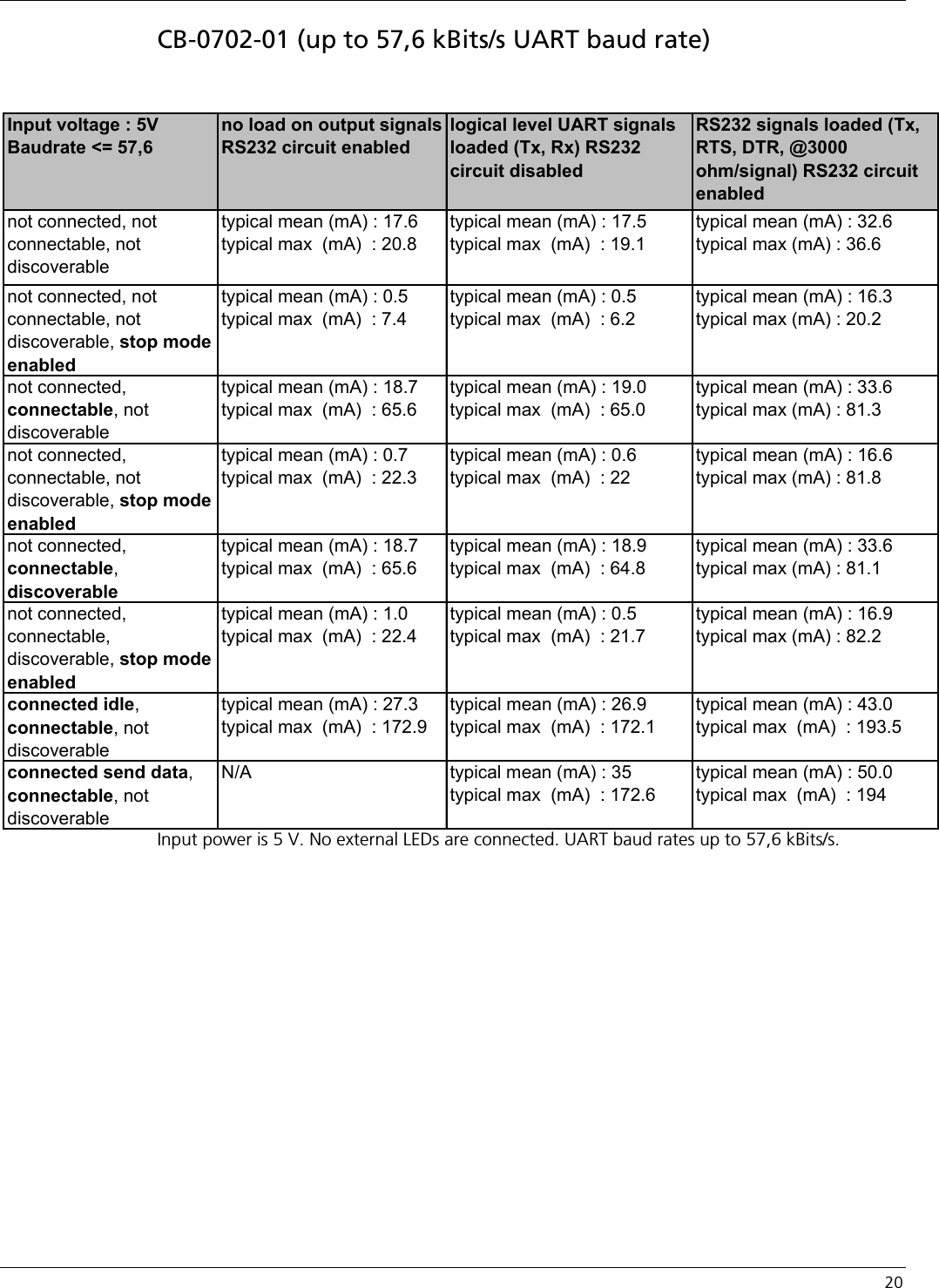
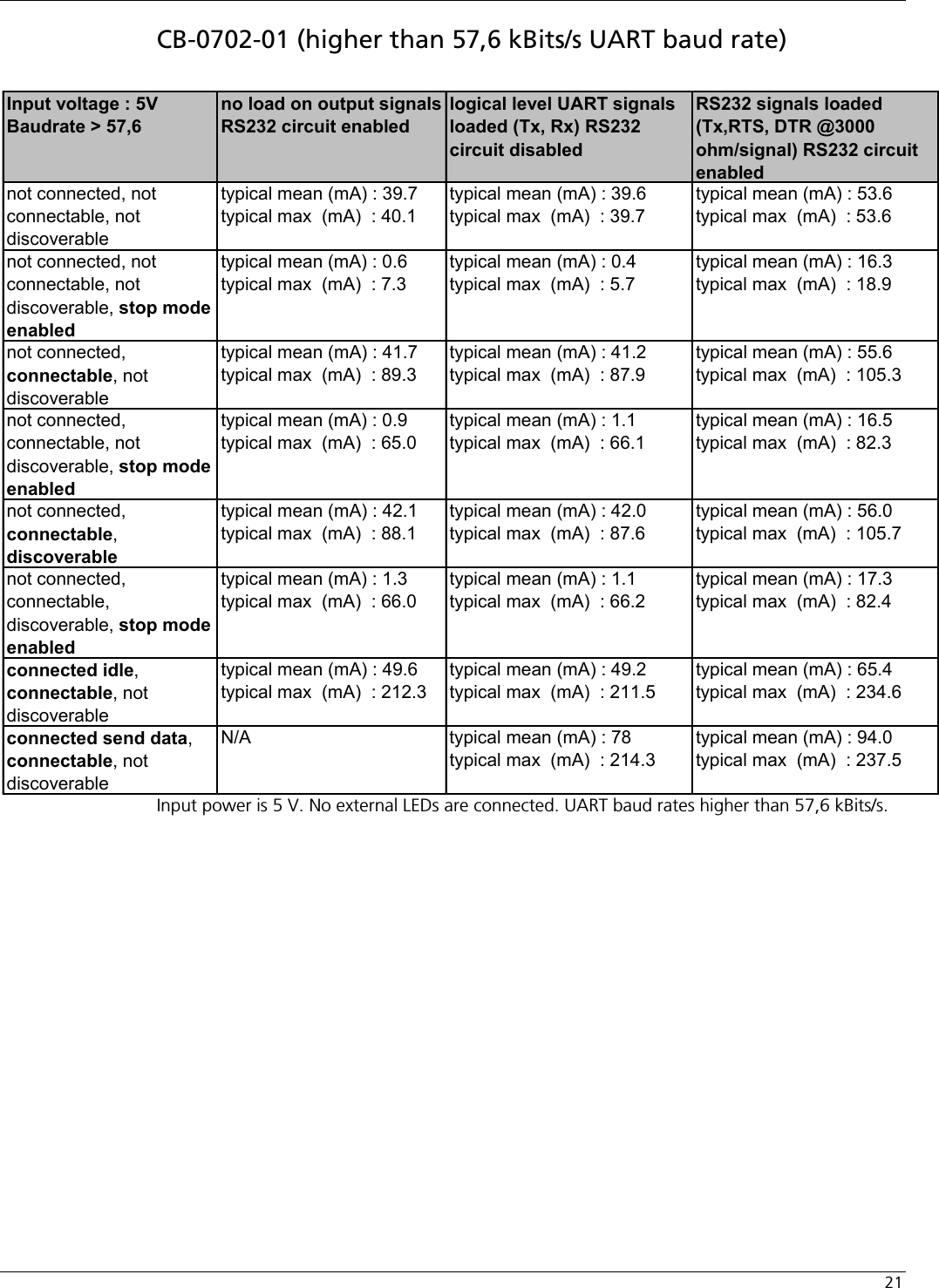
u blox Malmo 070101 Bluetooth module cB-0701-01 User Manual E M Datasheet OEMSPA Gen2
u-blox Malmo AB Bluetooth module cB-0701-01 E M Datasheet OEMSPA Gen2
UserManual.wiki
>
u blox Malmo
>
070101 User Manual
Users Manual
Navigation menu
Upload a User Manual
Namespaces
Wiki Guide
HTML
PDF
Info
Views
User Manual
Discussion / Help
Navigation
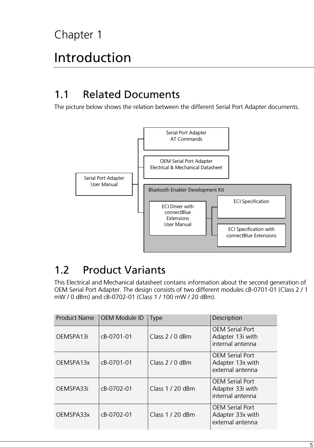
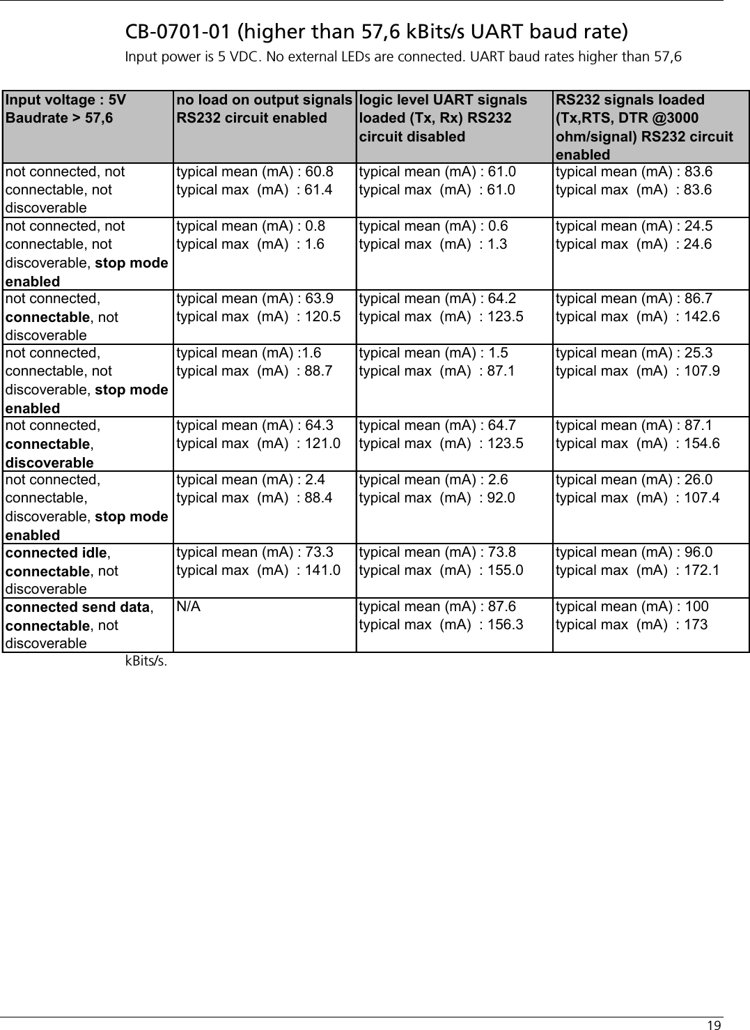
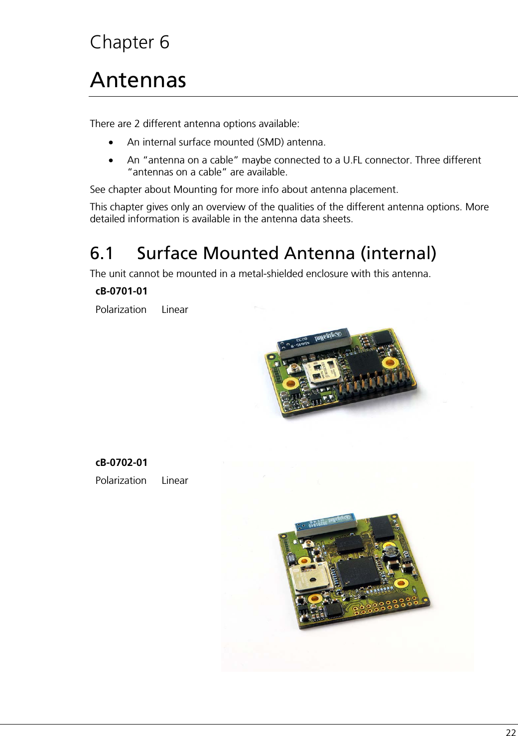
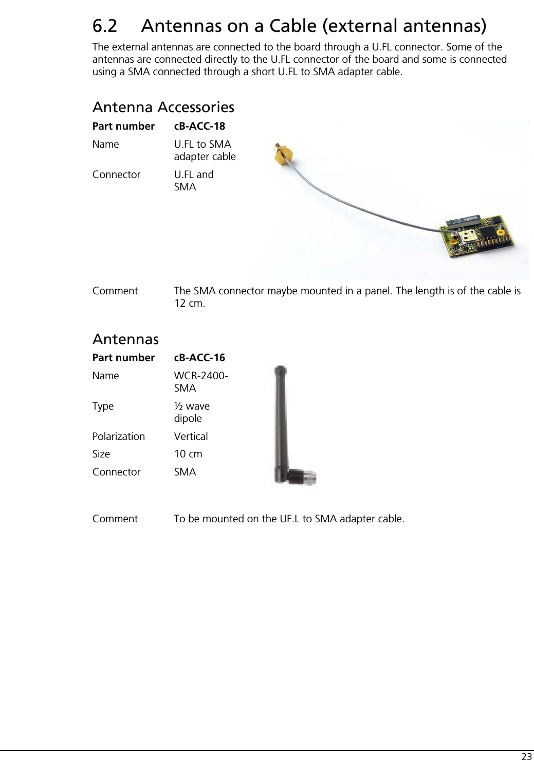
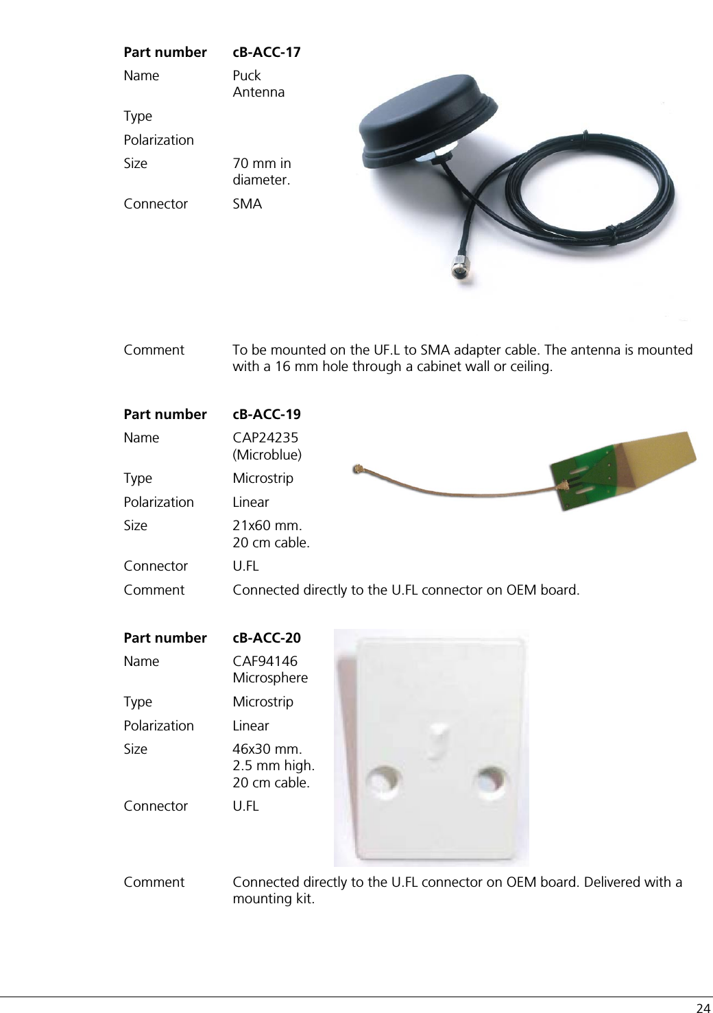
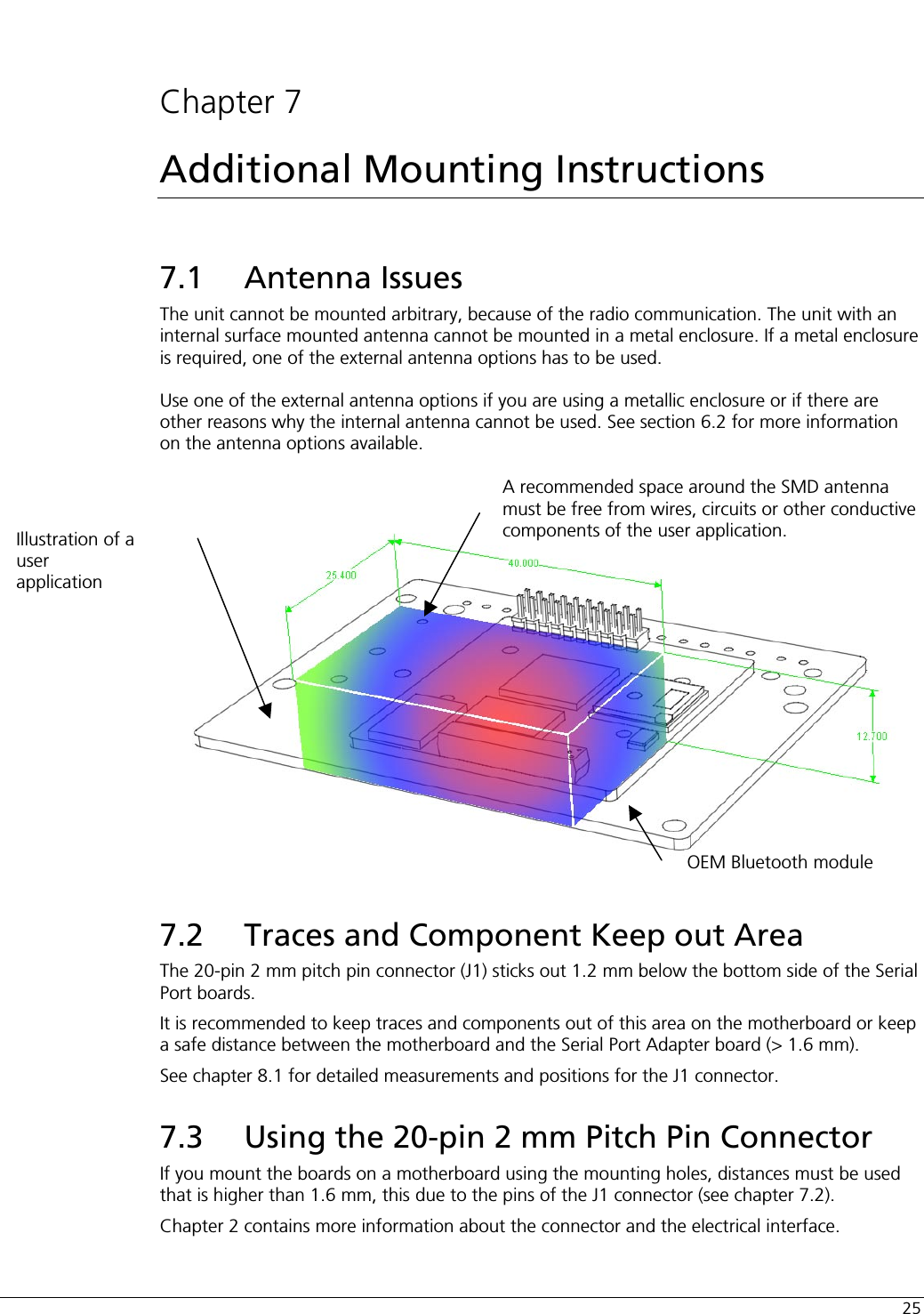
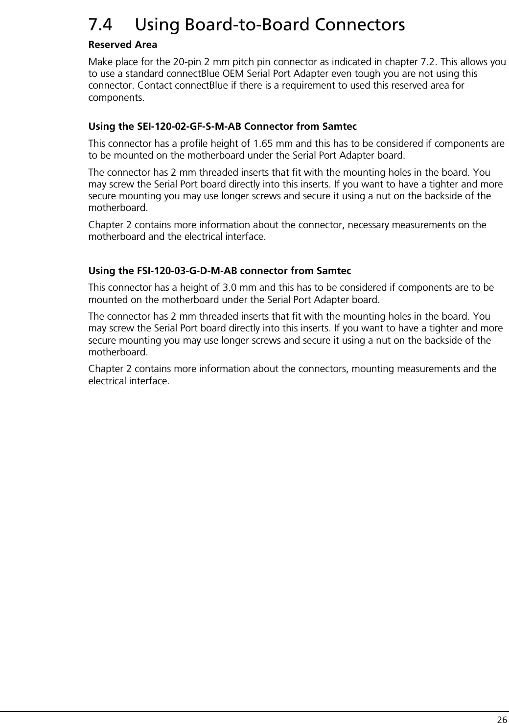
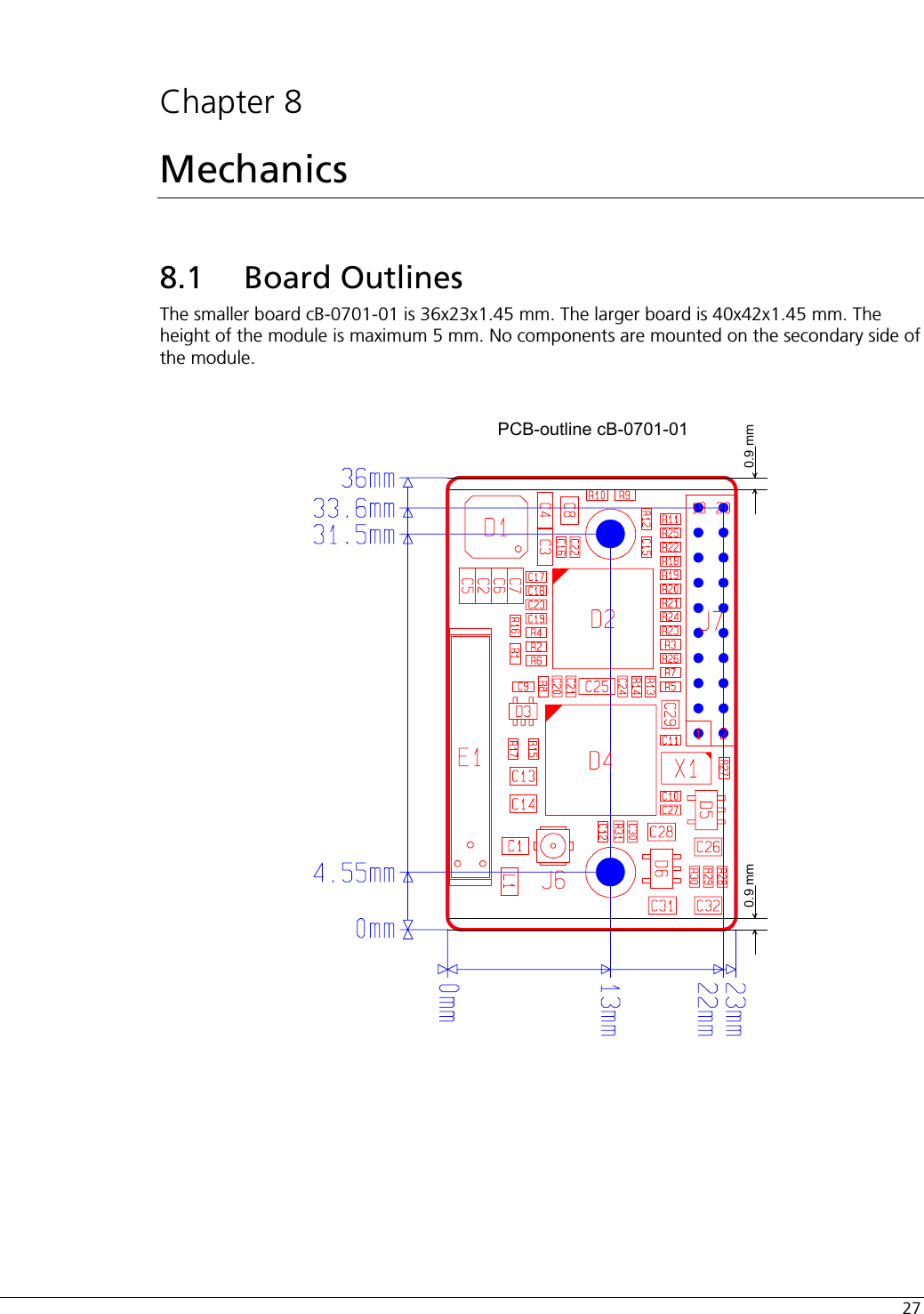
![7 1.3 Block Diagram cB-0701-01 1.4 Block Diagram cB-0702-01 ADR[1..22]DATA[0..15]ADR[0..19]DATA[0..7]Base Band ControllerPBM990 90 (BLINK)FLASH1 - 8MbyteSRAM128k - 1MbyteEBC radio interfaceRS-232TransceiverADM3315Bluetooth-RadioPBA313 02(MIRIAN)PowersupplyVin=3.3-6VModule InterfaceADR[0..23]DATA[0..15]Internal antennaExternal Antenna connectorJ1J2J4J5J3J6 Base Band ControllerPBM990 80 (FLINK)EBC radio interfaceRS-232TransceiverADM3315Bluetooth-RadioPBA313 05(RAN)PowersupplyVin=3.3-6VModule InterfaceInternal antennaExternal Antenna connectorJ1J2J3J6Vin=3-6V](https://usermanual.wiki/u-blox-Malmo/070101/User-Guide-308145-Page-7.png)