u blox Malmo 090202L Wireless Communication System User Manual E M Datasheet cB 0902
u-blox Malmo AB Wireless Communication System E M Datasheet cB 0902
UserManual.wiki
>
u blox Malmo
>
090202L User Manual
Integration Manual
Navigation menu
Upload a User Manual
Namespaces
Wiki Guide
HTML
PDF
Info
Views
User Manual
Discussion / Help
Navigation
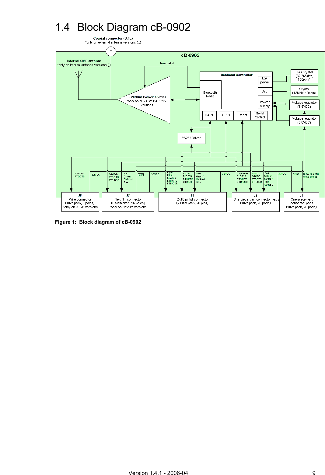
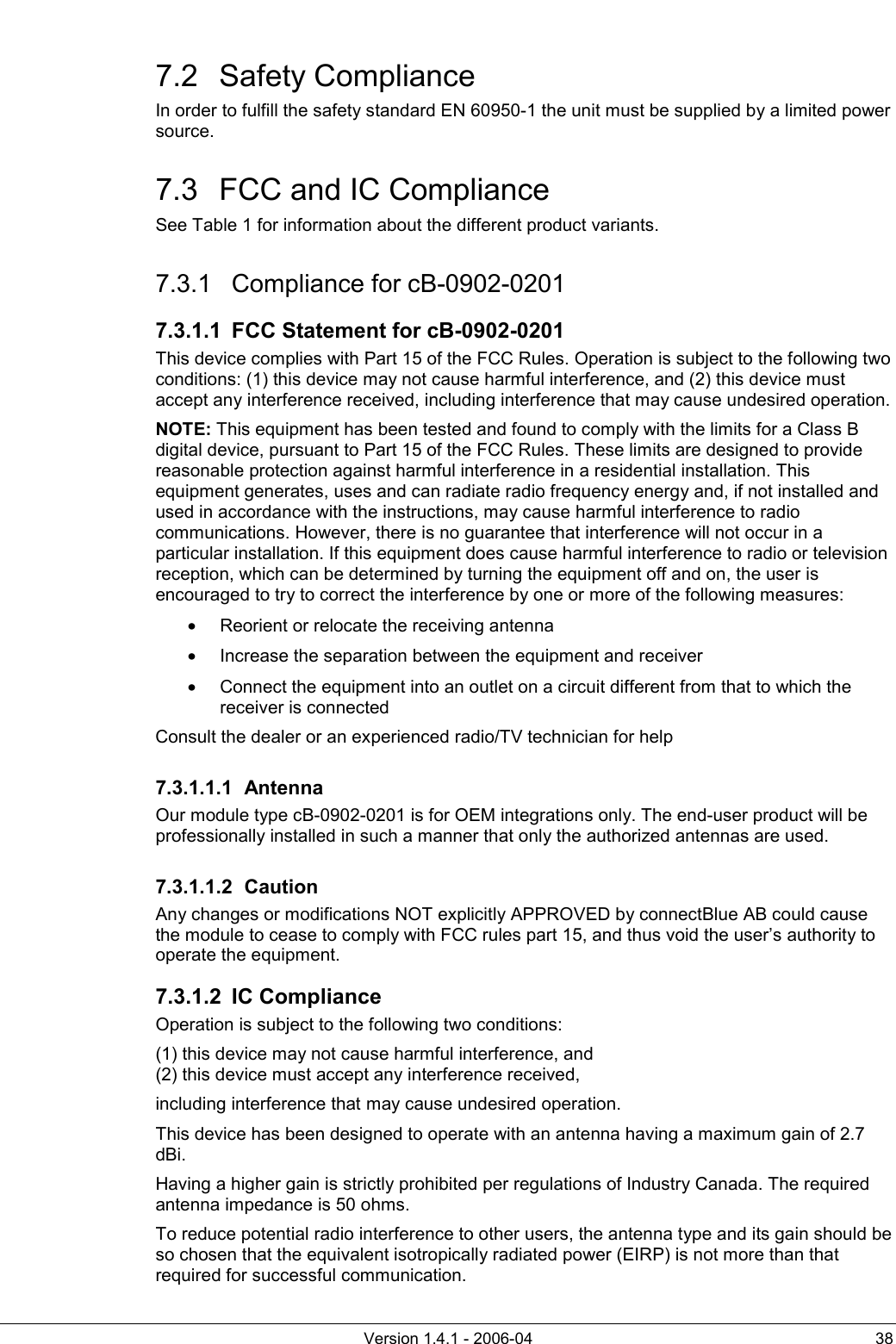
![Version 1.4.1 - 2006-04 28 5 Mounting Information 5.1 Board Outlines 5.1.1 cB-0902 Figure 5: cB-0902 dimensions [mm]. The J2 pads are longer to fit both the single and double row connec-tors (see section 5.2).](https://usermanual.wiki/u-blox-Malmo/090202L/User-Guide-668548-Page-28.png)
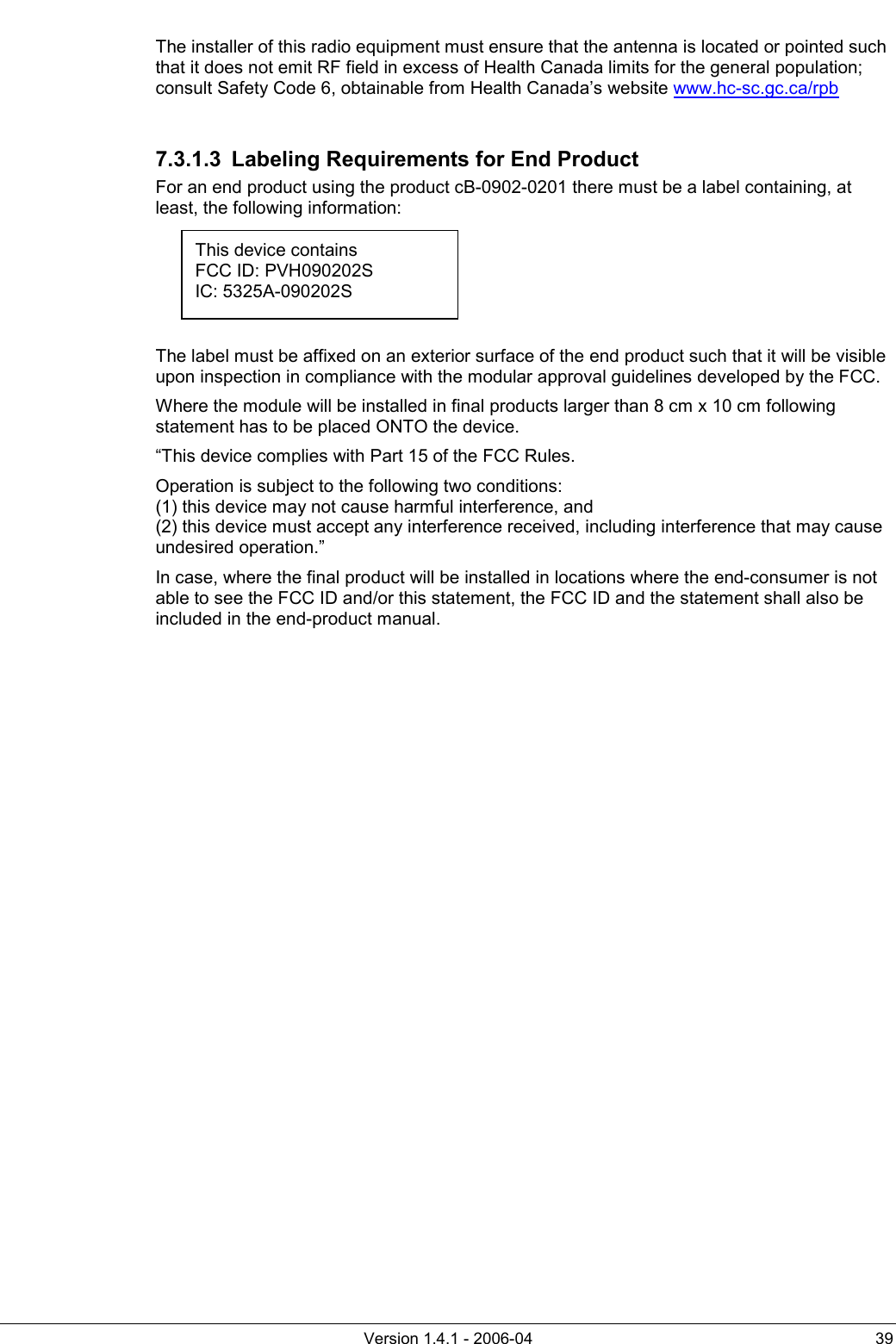
![Version 1.4.1 - 2006-04 29 5.1.2 Mounting Holes There are 2 x 2.3mm mounting holes on cB-0902. The reasons for the 2.3mm holes are that the threaded M2 holes on the single and double row connectors (see section 5.2.1) are not aligned. The outer tangents of the 2.3mm holes align the module if the single row connectors are used and the inner if double row connectors are used (see Figure 6). Choose the outer tangent (CC distance 27.24mm) if the module is aligned and mounted with some other technique based on M2 screws (e.g. press-fit nuts), see Figure 7 and Figure 8. Figure 6: The 2.3mm mounting holes [mm]](https://usermanual.wiki/u-blox-Malmo/090202L/User-Guide-668548-Page-29.png)
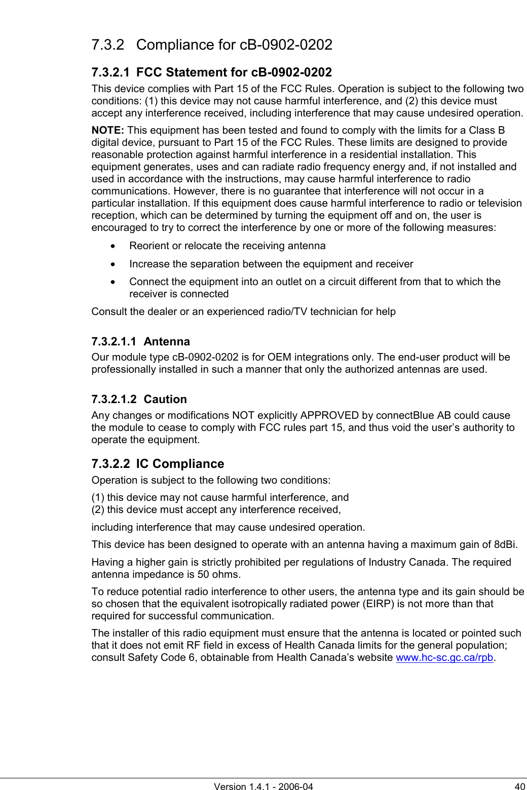
![Version 1.4.1 - 2006-04 31 Figure 7: Host PCB layout [mm] for single row connector.](https://usermanual.wiki/u-blox-Malmo/090202L/User-Guide-668548-Page-31.png)
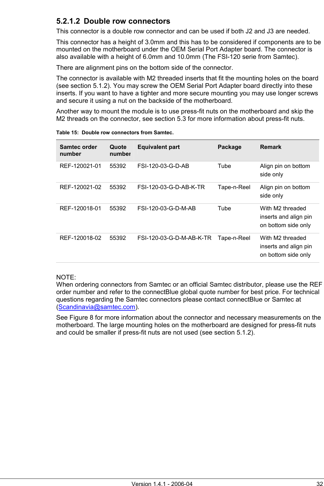
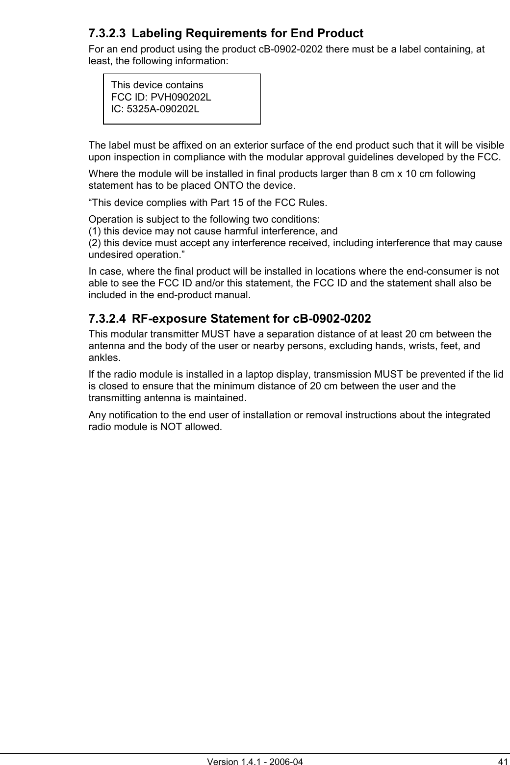
![Version 1.4.1 - 2006-04 33 Figure 8: Host PCB layout [mm] for double row connector.](https://usermanual.wiki/u-blox-Malmo/090202L/User-Guide-668548-Page-33.png)