u blox Malmo 090202L Wireless Communication System User Manual E M Datasheet cB 0902
u-blox Malmo AB Wireless Communication System E M Datasheet cB 0902
Integration Manual
INDUSTRIAL BLUETOOTH™
OEM Serial Port Adapter™
cB-0902
Electrical & Mechanical Datasheet
OEM Serial Port Adapter™
cB-0902
Electrical & Mechanical Datasheet
Copyright © 2005 connectBlue AB.
The contents of this document can be changed by connectBlue AB without prior
notice and do not constitute any binding undertakings from connectBlue AB.
connectBlue AB is not responsible under any circumstances for direct, indirect,
unexpected damage or consequent damage that is caused by this document.
All rights reserved.
Release: 2006-04
Document version: 1.4.1
Document number: cBProduct-0503-01
Printed in Sweden.
Trademarks
Registered trademarks from other companies are: Bluetooth is a trademark owned
by the Bluetooth SIG, Inc., Microsoft™, Windows™, Windows NT™,
Windows 2000™, Windows CE™, Windows ME™, are registered trademarks from
Microsoft Corporation.

Version 1.4.1 - 2006-04 4
Contents
1 Introduction 5
1.1 Related Documents ...........................................................................5
1.2 Product Variants ................................................................................6
1.3 cB-0902..............................................................................................8
1.4 Block Diagram cB-0902 .....................................................................9
2 Electrical Interface and Connectors 10
2.1 Pin Numbering .................................................................................11
2.2 Pin Description.................................................................................12
2.3 Characteristics .................................................................................18
2.4 Hardware Reset ...............................................................................22
2.5 Power Control ..................................................................................22
3 Operating Status 23
4 Antennas 24
4.1 Surface Mounted Antenna (Internal)................................................24
4.2 External antennas ............................................................................25
5 Mounting Information 28
5.1 Board Outlines .................................................................................28
5.2 Using the J2/J3 Board-to-Board Connectors ...................................30
5.3 Using Press-Fit Nuts for Mounting the Module ................................34
5.4 Antenna Issues ................................................................................34
6 Bluetooth Information 35
6.1 General information .........................................................................35
6.2 Bluetooth Qualification information ..................................................36
7 Regulatory Information 37
7.1 Declaration of Conformity ................................................................37
7.2 Safety Compliance ...........................................................................38
7.3 FCC and IC Compliance ..................................................................38
7.4 UL listing information .......................................................................42
7.5 Compliance with RoHS directive......................................................42
8 Guidelines for Efficient and Safe Use 43
8.1 General ............................................................................................43
8.2 Product Care ....................................................................................43
8.3 Radio Frequency Exposure .............................................................43
8.4 Electronic Equipment .......................................................................44
8.5 Potentially Explosive Atmospheres..................................................44
8.6 Power Supply ...................................................................................44
Appendix A - Application Notes 45
A.1 Step-by-Step Guide .........................................................................45
A.2 Design Examples .............................................................................46

Version 1.4.1 - 2006-04 5
1 Introduction
1.1 Related Documents
There are some documents related to the Serial Port Adapter:
- The Serial Port Adapter AT Commands document contains a description of the AT
commands supported in the Serial Port Adapter. It also contains information on how to
use the AT commands to create Bluetooth applications.
- The OEM Serial Port Adapter Electrical & Mechanical Datasheet (this document)
contains important information about the OEM Serial Port Adapter. Read this document
if you are using the OEM Serial Port Adapter.

Version 1.4.1 - 2006-04 6
1.2 Product Variants
This Electrical and Mechanical datasheet contains information about the 16 variants of OEM
Serial Port Adapters based on the PCB cB-0902. This document makes references to the
OEM Module ID, not the Product Name (see Table 1).
Table 1: Product variants
Product Name OEM Module ID /
FCC ID
Bluetooth Type Description
CB-OEMSPA312i-02 cB-0069
PVH090202S
Class 1 / +7dBm
5mW
OEM Serial Port Adapter
312i with internal antenna,
2mm pin connector
CB-OEMSPA312i-04 cB-0070
PVH090202S
Class 1 / +7dBm
5mW
OEM Serial Port Adapter
312i with internal antenna,
no connectors
CB-OEMSPA312i-06 cB-0071
PVH090202S
Class 1 / +7dBm
5mW
OEM Serial Port Adapter
312i with internal antenna,
JST 6-pol
Class 1 +7dBm
Internal antenna
CB-OEMSPA312i-07 cB-0072
PVH090202S
Class 1 / +7dBm
5mW
OEM Serial Port Adapter
312i with internal antenna,
Flexfilm
CB-OEMSPA312x-02 cB-0073
PVH090202S
Class 1 / +7dBm
5mW
OEM Serial Port Adapter
312x with external antenna,
2mm pin connector
CB-OEMSPA312x-04 cB-0074
PVH090202S
Class 1 / +7dBm
5mW
OEM Serial Port Adapter
312x with external antenna,
no connectors
CB-OEMSPA312x-06 cB-0075
PVH090202S
Class 1 / +7dBm
5mW
OEM Serial Port Adapter
312x with external antenna,
JST 6-pol
Class 1 +7dBm
External antenna
CB-OEMSPA312x-07 cB-0076
PVH090202S
Class 1 / +7dBm
5mW
OEM Serial Port Adapter
312x with external antenna,
Flexfilm
CB-OEMSPA332i-02 cB-0077
PVH090202L
Class 1 / +16.9dBm
49mW
OEM Serial Port Adapter
332i with internal antenna,
2mm pin connector
CB-OEMSPA332i-04 cB-0078
PVH090202L
Class 1 / +16.9dBm
49mW
OEM Serial Port Adapter
332i with internal antenna,
no connectors
CB-OEMSPA332i-06 cB-0079
PVH090202L
Class 1 / +16.9dBm
49mW
OEM Serial Port Adapter
332i with internal antenna,
JST 6-pol
Class 1 +17dBm
Internal antenna
CB-OEMSPA332i-07 cB-0080
PVH090202L
Class 1 / +16.9dBm
49mW
OEM Serial Port Adapter
332i with internal antenna,
Flexfilm

Version 1.4.1 - 2006-04 7
Product Name OEM Module ID /
FCC ID
Bluetooth Type Description
CB-OEMSPA332x-02 cB-0081
PVH090202L
Class 1 / +16.9dBm
49mW
OEM Serial Port Adapter
332x with external antenna,
2mm pin connector
CB-OEMSPA332x-04 cB-0082
PVH090202L
Class 1 / +16.9dBm
49mW
OEM Serial Port Adapter
332x with external antenna,
no connectors
CB-OEMSPA332x-06 cB-0083
PVH090202L
Class 1 / +16.9dBm
49mW
OEM Serial Port Adapter
332x with external antenna,
JST 6-pol
Class 1 +17dBm
External antenna
CB-OEMSPA332x-07 cB-0084
PVH090202L
Class 1 / +16.9dBm
49mW
OEM Serial Port Adapter
332x with external antenna,
Flexfilm
Version 1.4.1 - 2006-04 8
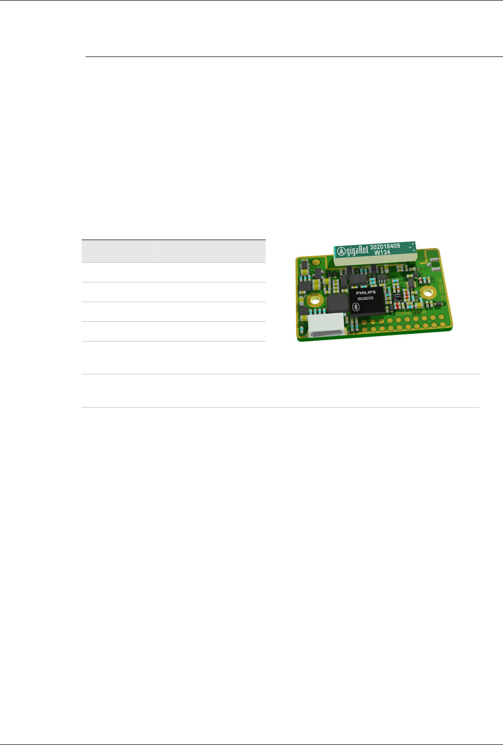
1.3 cB-0902
cB-0902 is a small size Bluetooth module based on the Phillips BGB203 system in package
(SiP). The BGB203 has on chip SRAM and FLASH stacked in the same package. The
modules are available in many variants with different antenna / connectors and output power
combinations. See Picture 1 - Picture 3 for some of the available models. All models are
described in Table 1.
The cB-0902 has an RS232 interface and is fully compatible with the connectBlue 2:nd
Generation Class 2 Serial Port Adapter.
Picture 1: CB-OEMSPA332x-02
OEM Serial Port Adapter long
range with external antenna and
2mm pin connector
Picture 2: CB-OEMSPA332i-06
OEM Serial Port Adapter long
range with internal antenna and
JST connector
Picture 3: CB-OEMSPA312i-07
OEM Serial Port Adapter short
range with internal antenna and
Flexfilm connector
Version 1.4.1 - 2006-04 9
1.4 Block Diagram cB-0902
Figure 1: Block diagram of cB-0902
Version 1.4.1 - 2006-04 10
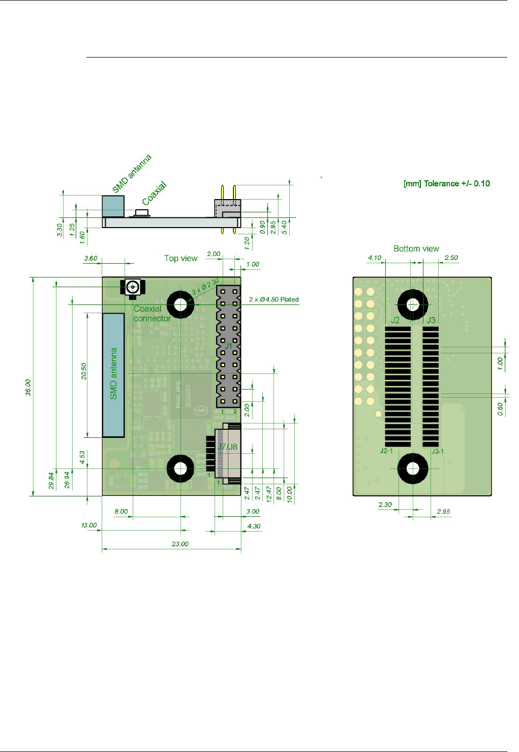
2 Electrical Interface and Connectors
This section describes the signals available on the module interface connectors.
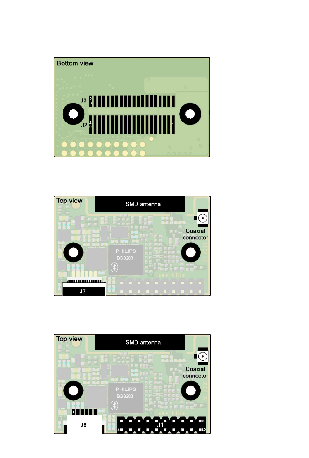
There are four ways to connect to the OEM Serial Port Adapter:
• Via the 2x10-pin 2mm header connector J1 (see Picture 4).
• Via the 2x20-pin 1mm pitch board-to-board (one piece part) connectors, J2 through
J3. The J2 to J3 connectors on the OEM Serial Port Adapter exist on the module
only as a mating PCB-layout pattern (see Picture 5). See Section 5.2 for more
information.
Optional:
• Via the flexfilm connector, J7 (see Picture 6). The connector is a 16 poles flexfilm
connector. The pitch is 0.5mm and the flexfilm should be 0.3mm thick. The
connector is from Hirose with part number FH19S-16S-0.5SH(05).
• Via the JST connector, J8 (see Picture 7). The connector is a 6 poles wire
connector. The pitch is 1mm and the. The connector is from JST with part number
SM06B-SRSS-TB.
Picture 4: 2x20 2mm pinlist connector, J1. Picture 5: J2 to J3 are available on cB-0902.
Picture 6: Flexfilm connector, J7. Picture 7: JST 6-pol connector, J8.
J1
J7 J8
J3
J2
Version 1.4.1 - 2006-04 11
2.1 Pin Numbering
2.1.1 J2 and J3
Figure 2: Bottom view of the PCB with the pinning of the J2 and J3 pads connector.
2.1.2 Flexfilm J7
Figure 3: Top view of the PCB with the pinning of the J7 connector.
2.1.3 Pinlist J1 and JST 6-pol J8
Figure 4: Top view of the PCB with the pinning of the J1 and J8 connector.

Version 1.4.1 - 2006-04 12
2.2 Pin Description
2.2.1 J1 & J2 Connector
Table 2: Signals on J1 and J2.
J1&J2
Pin Nr
Pin Name Signal Name Signal
Level
Type Description
1-2 VSS Ground Ground GND
3-4 VCC_3V3 Power 3.3V 3.0 – 6.0 VDC for
CB-OEMSPA312 modules
3.3 – 6.0 VDC for
CB-OEMSPA332 modules
5 RS232-CTS Clear To Send RS232 In Hardware flow control
6 RS232-TxD Transmit Data RS232 Out
7 RS232-RTS Request To Send RS232 Out Hardware flow control
8 RS232-RxD Receive Data RS232 In
9 RS232-DTR Data Terminal Ready RS232 Out
10 RS232-DSR Data Set Ready RS232 In Also used to control the power
saving mode “stop mode”.
See section 2.5 for more informa-
tion.
11 RED/Mode Red LED output CMOS In/Out This signal is multiplexed:
RED:
Logic Red LED Signal (see Chap-
ter 3, Table 13). Pin is used as
input for approximately 500ms at
startup.
Mode:
The level on this pin during power
up selects RS232 (High) or logic
(Low) level UART-communication.
The Mode pin is only valid during
the first 500ms after startup and
cannot be changed during opera-
tion.
The Mode pin is internally pulled
up i.e. RS232 mode is the default
setting. Recommended value of
the pull-down resistor is 1kΩ**.
See section A.2.3.2 for design
examples.

Version 1.4.1 - 2006-04 13
J1&J2
Pin Nr
Pin Name Signal Name Signal
Level
Type Description
12 Switch-0 Function switch CMOS In Used for the “Connect on external
signal” function, see the Serial Port
Adapter AT command Specifica-
tion for more information on the
Function switch.
See section A.2.3.4 for design
examples.
13 GREEN/
Switch-1
Green LED output and
Restore switch
CMOS In/Out This signal is multiplexed:
GREEN:
Logic Green LED Signal (see
Chapter 3, Table 13). Not valid
until 500ms after startup.
Switch-1:
If the level on this pin is pulled-
down with 1kΩ** the units goes
back to default serial settings.
The “Restore Default” input is only
active during the first 500ms after
startup.
See the Serial Port Adapter AT
command Specification for more
information on the Restore switch.
See section A.2.3.3 for design
examples.
14 BLUE Blue LED output CMOS Out Logic Blue LED Signal (see Chap-
ter 3, Table 13).
Note:
Signal will flicker at data transmis-
sion.
See section A.2.3.1 for design
examples.
15 UART-CTS* Clear To Send CMOS In Hardware flow control.
16 UART-TxD* Transmit Data CMOS Out
17 UART-RTS* Request To Send CMOS Out Hardware flow control.
18 UART-RxD* Receive Data CMOS In
19 UART-DTR* Data Terminal Ready CMOS Out
20 UART-DSR* Data Set Ready CMOS In
* All signals are logic level UART signals (typically 0 - 3VDC)
** Use 1kΩ as pull-down which is different to previous product generations from connectBlue

Version 1.4.1 - 2006-04 14
2.2.2 J3 Connector
Table 3: Signals on J3
J3
Pin Nr
Pin Name Signal Name Signal
Level
Type Description
1-8 Reserved, do not connect.
9 SerialSelect-0 Serial Select 0 CMOS Out Control signal for external serial
transceivers. See section
A.2.2.4 for more info.
10 SerialSelect-1 Serial Select 1 CMOS Out Control signal for external serial
transceivers. See section
A.2.2.4 for more info.
11-18 Reserved, do not connect.
19 RESET Hardware reset CMOS In Active low. Must be open drain
collector.
See section 2.4 for design ex-
amples.
20 Reserved, do not connect.

Version 1.4.1 - 2006-04 15
2.2.3 J7 Connector (Flexfilm)
NOTE! The physical serial interface on J7 is RS232, which is different compared to the cB-
OEMSPA311i/x and cB-OEMSPA331i/x products.
Table 4: Signals on J7
J7
Pin Nr
Pin Name Signal Name Signal
Level
Type Description
1 RESET Hardware reset CMOS In Active low. Must be open drain
collector.
See section 2.4 for design ex-
amples.
2 RS232-DSR Data Set Ready RS232 In
3 VSS Ground Ground GND
4 VCC_3V3 Power 3.3V 3.0 – 6.0 VDC for
CB-OEMSPA312 modules
3.3 – 6.0 VDC for
CB-OEMSPA332 modules
5 RS232-DTR Data Terminal Ready RS232 Out
6 RED/Mode Red LED output CMOS Out This signal is multiplexed:
RED:
Logic Red LED Signal (see
Chapter 3, Table 13). Pin is
used as input for approximately
500ms at startup.
Mode:
The level on this pin during
power up selects RS232 (High)
or logic (Low) level UART-
communication.
The Mode pin is only valid dur-
ing the first 500ms after startup
and cannot be changed during
operation.
The Mode pin is internally
pulled up i.e. RS232 mode is
the default setting. Recom-
mended value of the pull-down
resistor is 1kΩ**.
See section A.2.3.2 for design
examples.

Version 1.4.1 - 2006-04 16
J7
Pin Nr
Pin Name Signal Name Signal
Level
Type Description
7 GREEN/
Switch-1
Green LED output and
Restore switch
CMOS In/Out This signal is multiplexed:
GREEN:
Logic Green LED Signal (see
Chapter 3, Table 13). Not valid
until 500ms after startup.
Switch-1:
If the level on this pin is pulled-
down with 1kΩ** the units goes
back to default serial settings.
The “Restore Default” input is
only active during the first
500ms after startup.
See the Serial Port Adapter AT
command Specification for
more information on the Re-
store switch.
See section A.2.3.3 for design
examples.
8 BLUE Blue LED output CMOS Out Logic Blue LED Signal (see
Chapter 3, Table 13).
Note:
Signal will flicker at data trans-
mission.
See section A.2.3.1 for design
examples.
9 RS232-TxD Transmit Data RS232 Out
10 RS232-RxD Receive Data RS232 In
11 RS232-CTS Clear To Send RS232 In Hardware flow control
12 RS232-RTS Request To Send RS232 Out Hardware flow control
13-16 Reserved, do not connect.
** Use 1kΩ as pull-down which is different to previous product generations from connectBlue

Version 1.4.1 - 2006-04 17
2.2.4 J8 Connector (JST 6-pol)
NOTE! The physical serial interface on J8 is RS232, which is different compared to the cB-
OEMSPA311i/x and cB-OEMSPA331i/x products.
Table 5: Signals on J8
J8
Pin Nr
Pin Name Signal Name Signal
Level
Type Description
1 VSS Ground Ground GND
2 VCC_3V3 Power 3.3V 3.0 – 6.0 VDC for
CB-OEMSPA312 modules
3.3 – 6.0 VDC for
CB-OEMSPA332 modules
3 RS232-TxD Transmit Data RS232 Out
4 RS232-RxD Receive Data RS232 In
5 RS232-CTS Clear To Send RS232 In Hardware flow control
6 RS232-RTS Request To Send RS232 Out Hardware flow control

Version 1.4.1 - 2006-04 18
2.3 Characteristics
The cB-0902 board is designed to be fully interchangeable. If the host product has space for
the board it is possible to choose freely between a cB-OEMSPA312i/x or cB-OEMSPA332i/x
device without any change of the host product. If you design your power supply for cB-
OEMSPA332i/x the modules will be fully interchangeable.
The cB-0902 module has a linear power supply, which means that the current is constant if
the voltage supply is changed. See Table 9.
For more information about low power modes see Serial Port Adapter AT commands
Specification.
2.3.1 Power supply
NOTE: Read the safety notes in section 7.2 before using the modules.
2.3.1.1 cB-OEMSPA312i/x products
Table 6: Power supply
Symbol Parameter Value Unit
Min 3.0 VDC VCC_3V3 Power supply (Unregulated*)
Max 6.0 VDC
* The module is equipped with an internal linear voltage regulator.
Table 7: Current consumption
Symbol Mode Value Unit
Average 7.9 mA Not connected
Peak 48 mA
Average 1.0 mA Not connectable
Peak 1.2 mA
Average 1.8 mA Connectable
Peak 48 mA
Average 1.8 mA
Not con-
nected, stop
mode en-
abled
Connectable,
discoverable Peak 48 mA
Average 17 mA Idle or Receiving
Peak 55 mA
Average 22 mA
Connected
Transmitting
@115.2kbit/s Peak 58 mA
Average 39 mA
ICC
@ VCC_3V3 = 3.3V
Inquiry
Peak 70 mA
IRS232 Output1 RS232 Average 7 mA
RRS232 load2 RS232 Typ 20 kΩ
1 RS232 output signals TxD, RTS, DTR loaded with 3kΩ. Not included in ICC, very dependent on the load.
2 Internal load on each RS232 input pin.

Version 1.4.1 - 2006-04 19
2.3.1.2 cB-OEMSPA332i/x products
Table 8: Power supply
Symbol Parameter Value Unit
Min 3.3 VDC VCC_3V3 Power supply (Unregulated*)
Max 6.0 VDC
* The module is equipped with an internal linear voltage regulator.
Table 9: Current consumption
Symbol Mode Value Unit
Average 19 mA Not connected
Stop mode not enabled. Peak 63 mA
Average 10 mA Not connectable
Peak 13 mA
Average 11 mA Connectable
Peak 60 mA
Average 11 mA
Not con-
nected, stop
mode en-
abled
Connectable,
discoverable Peak 60 mA
Average 22 mA Idle or Receiving
Peak 170 mA
Average 53 mA
Connected
Transmitting
@115.2kbit/s Peak 170 mA
Average 84 mA
ICC
@ VCC_3V3 = 3.3V
Inquiry
Peak 150 mA
IRS232 Output1 RS232 Average 7 mA
RRS232 load2 RS232 Typ 20 kΩ
1 RS232 output signals TxD, RTS, DTR loaded with 3kΩ. Not included in ICC, very dependent on the load.
2 Internal load on each RS232 input pin.

Version 1.4.1 - 2006-04 20
2.3.2 Input/Output signals
2.3.2.1 cB-OEMSPA312i/x products
Table 10: Input/output signals
Symbol Parameter Value Unit
Min -0.4 V Logic LOW level input voltage on all logic
input pins except Switch-0 Max 0.80 V
Min -0.4 V
VIN Low
Logic LOW level input voltage Switch-0
Max 0.15 V
Min 2.05 V VIN High Logic HIGH level input voltage
Max 3.35 V
VOUT Low Logic LOW level output voltage Max 0.4 V
VOUT High Logic HIGH level output voltage Min 2.42 V
IGPIO Sink and source current Max 4 mA
2.3.2.2 cB-OEMSPA332i/x products
Table 11: Input/output signals
Symbol Parameter Value Unit
Min -0.4 V Logic LOW level input voltage on all logic
input pins except Switch-0 Max 0.85 V
Min -0.4 V
VIN Low
Logic LOW level input voltage Switch-0
Max 0.15 V
Min 2.15 V VIN High Logic HIGH level input voltage
Max 3.45 V
VOUT Low Logic LOW level output voltage Max 0.4 V
VOUT High Logic HIGH level output voltage Min 2.55 V
IGPIO Sink and source current Max 4 mA

Version 1.4.1 - 2006-04 21
2.3.3 Environmental
Table 12: Temperatures characteristics
Parameter Product Variant Value Unit
Min All -40 °C Storage temperature
Max All +125 °C
CB-OEMSPA312i/x-02
CB-OEMSPA332i/x-02
CB-OEMSPA312i/x-04
CB-OEMSPA332i/x-04
CB-OEMSPA312i/x-07
CB-OEMSPA332i/x-07
-30 °C
Min
CB-OEMSPA312i/x-06
CB-OEMSPA332i/x-06
-25 °C
CB-OEMSPA312i/x-02
CB-OEMSPA332i/x-02
CB-OEMSPA312i/x-04
CB-OEMSPA332i/x-04
CB-OEMSPA312i/x-06
CB-OEMSPA332i/x-06
+85 °C
Maximum operating temperature
Max
CB-OEMSPA312i/x-07
CB-OEMSPA332i/x-07
+80 °C

Version 1.4.1 - 2006-04 22
2.4 Hardware Reset
A hardware RESET input is available on the J3 and J7 connectors (see section 2.1). An
external reset source must be open drain collector, see section A.2.4 for design examples.
The RESET pin is internally pulled-up with 120kΩ.
2.5 Power Control
For more information about “Stop Mode” and other low power modes, see the Serial Port
Adapter AT command Specification.

Version 1.4.1 - 2006-04 23
3 Operating Status
The module can be in different modes (see the Serial Port Adapter AT command
Specification for more information about the modes) and the RED, GREEN and BLUE
signals can be used to detect or indicating the status, see Table 13. The LED signals are
active LOW.
Table 13: Signal states in different module modes
Serial Port Adapter Mode Status RGB LED
Color
GREEN
GPIO
BLUE
GPIO
RED
GPIO
Data mode IDLE Green LOW HIGH HIGH
AT mode IDLE Orange LOW HIGH LOW
Data mode, AT mode CONNECTING* Purple HIGH LOW LOW
Data mode, AT mode CONNECTED* Blue HIGH LOW HIGH
* On data activity the active LEDs flashes and will be HIGH for 50-100ms. For information on how to suppress the
flashes see section A.2.3.1.
DTR signal can be set to indicate an active Bluetooth link. For more information see Serial Port Adapter AT
command Specification.
Version 1.4.1 - 2006-04 24
4 Antennas
There are 2 different antenna options available:
• An internal surface mounted (SMD) antenna.
• An external antenna should be connected to a U.FL connector. Many different
external antennas are available.
See section 5.1 for more information on antenna placement.
This chapter gives an overview of the different antenna options.
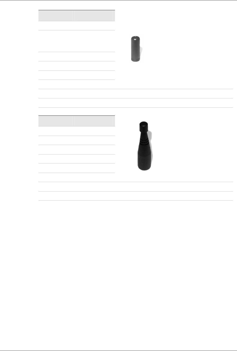
4.1 Surface Mounted Antenna (Internal)
The unit cannot be mounted in a metal-shielded enclosure with this antenna.
Part Number OEMSPA 312i / 332i
Antenna name Mica 2.4 GHz
Manufacture gigaAnt
Polarization Linear
Gain +2.5dBi
Antenna size
(LxWxH)
20.5x3.6x3.3 mm
Comment The antenna gain is dependent of the mounting of the module.
See section 5.4 for mounting the module considering the antenna.
Version 1.4.1 - 2006-04 25
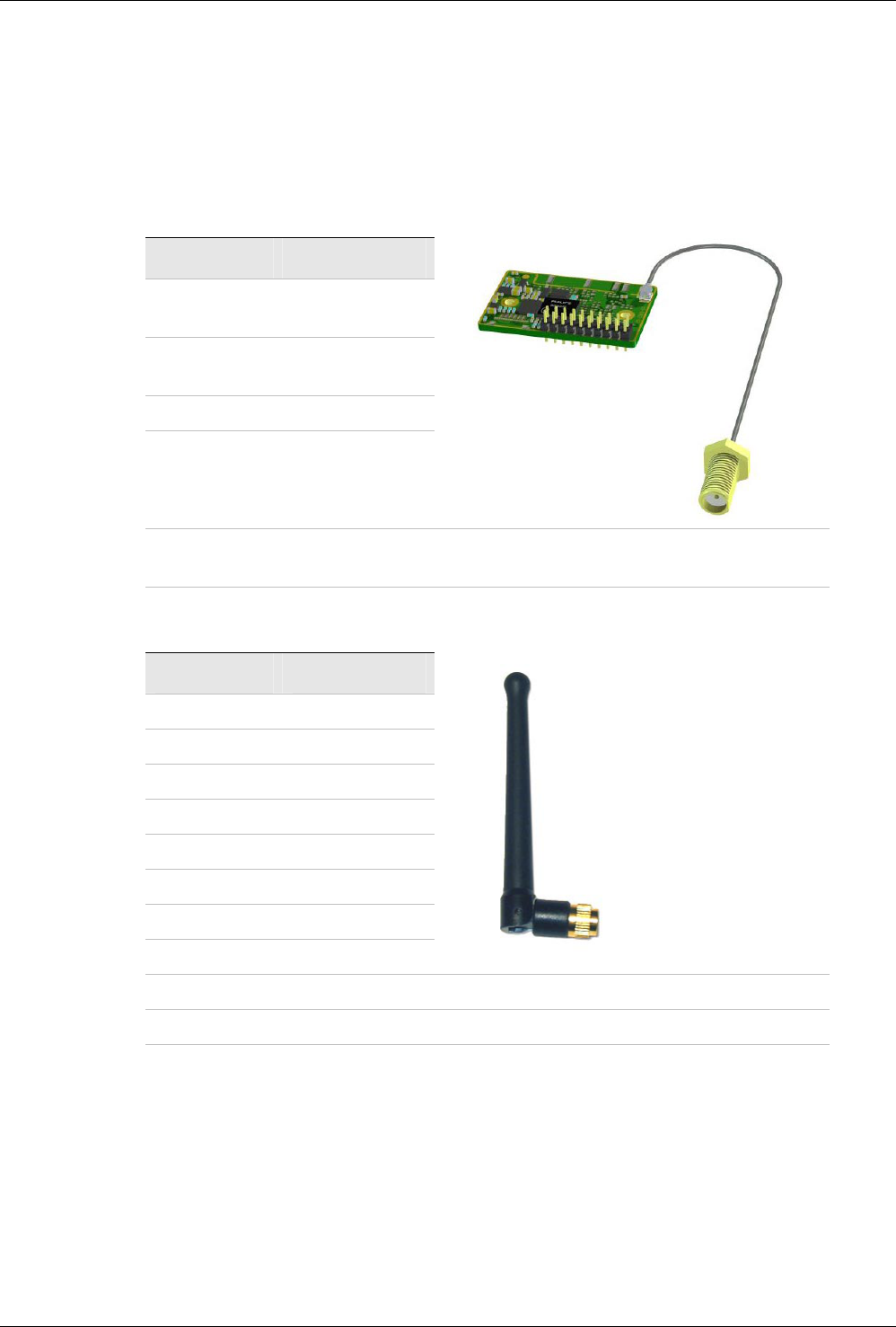
4.2 External antennas
The external antennas are connected to the board through a U.FL connector. Some of the
antennas are connected directly to the U.FL connector of the board and some are connected
using an SMA connected through a short U.FL to SMA adapter cable.
4.2.1 Antenna Accessories
Part Number cB-ACC-18
Name U.FL to SMA
adapter cable
Connector U.FL and
SMA female
Cable length 120 mm
Cable loss Less than 0.5dB
Comment The SMA connector may be mounted in a panel. Not approved for use in
the US and Canada.
4.2.2 Antennas
Part Number cB-ACC-16
Name WCR-2400-SMA
Manufacture Centurion
Type ½ wave dipole
Polarization Vertical
Gain +2.5dBi
Size 100 mm (Straight)
Connector SMA male
Comment To be mounted on the U.FL to SMA adapter cable.
Approval Not approved for use in the US and Canada.
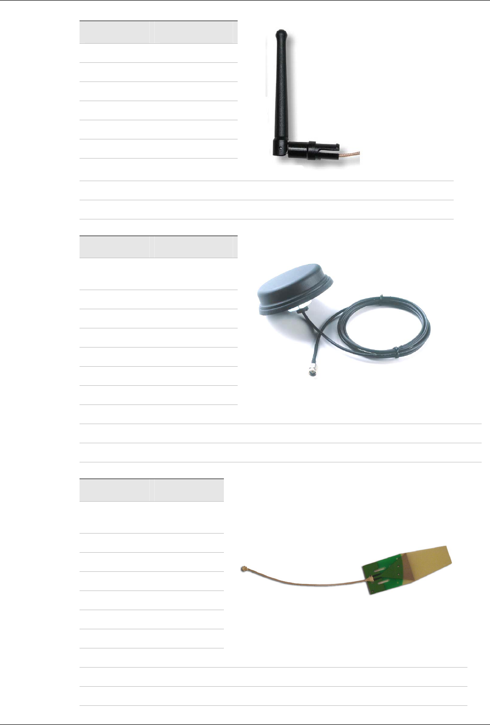
Version 1.4.1 - 2006-04 26
Part Number cB-ACC-27
Name WCR-2400-IP04
Manufacture Centurion
Type ½ wave dipole
Polarization Vertical
Gain +2.0dBi
Size 108 mm (Straight)
Connector U.FL connector
Comment To be mounted on the U.FL connector on the PCB.
Approval Approved for use in the US and Canada
Part Number cB-ACC-17
Name Reel planTec
Bluetooth m70
Manufacture Reel
Size (∅xH) 75x20 mm
Gain +1dBi
Mounting M16x13.6 mm
Cable length 3 m
Connector SMA male
Other info Waterproof (IP67)
Comment To be mounted on the U.FL to SMA adapter cable.
Approval Not approved for use in the US and Canada.
Part Number cB-ACC-19
Name Microblue
CAP24235
Manufacture Centurion
Type Microstrip
Polarization Linear
Gain +1.5dBi
Size 21x60 mm
Cable length 200 mm
Connector U.FL
Comment Connected directly to the U.FL connector on OEM board.
Approval Approved for use in the US and Canada
Version 1.4.1 - 2006-04 27
Part Number cB-ACC-23
Name Mobile Mark Stub
Manufacture Mobile Mark
Communications
Antennas
Type ¼ wave dipole
Polarization Vertical
Gain 0dBi
Connector SMA male
Comment To be mounted on the U.FL to SMA adapter cable
Approval Not approved for use in the US and Canada.
Part Number cB-ACC-21
Name Rugged SMA
Manufacture Radiall/Larsen
Type ½ wave dipole
Polarization Vertical
Gain 2dBi
Connector SMA male
Comment To be mounted on the U.FL to SMA adapter cable
Approval Not approved for use in the US and Canada.
Version 1.4.1 - 2006-04 29
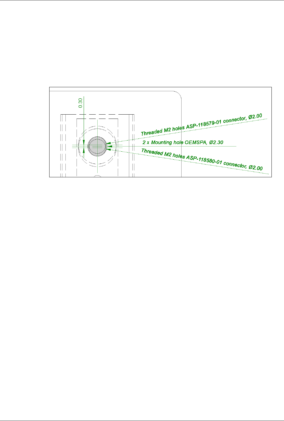
5.1.2 Mounting Holes
There are 2 x 2.3mm mounting holes on cB-0902. The reasons for the 2.3mm holes are that
the threaded M2 holes on the single and double row connectors (see section 5.2.1) are not
aligned. The outer tangents of the 2.3mm holes align the module if the single row connectors
are used and the inner if double row connectors are used (see Figure 6).
Choose the outer tangent (CC distance 27.24mm) if the module is aligned and mounted with
some other technique based on M2 screws (e.g. press-fit nuts), see Figure 7 and Figure 8.
Figure 6: The 2.3mm mounting holes [mm]

Version 1.4.1 - 2006-04 30
5.2 Using the J2/J3 Board-to-Board Connectors
The board-to-board connector should be a 1mm pitch one-piece part connector. The
recommended manufacture is Samtec with many connector options available; see section
5.2.1.1 and 5.2.1.2.
Chapter 2 contains more information about the connector and the electrical interface.
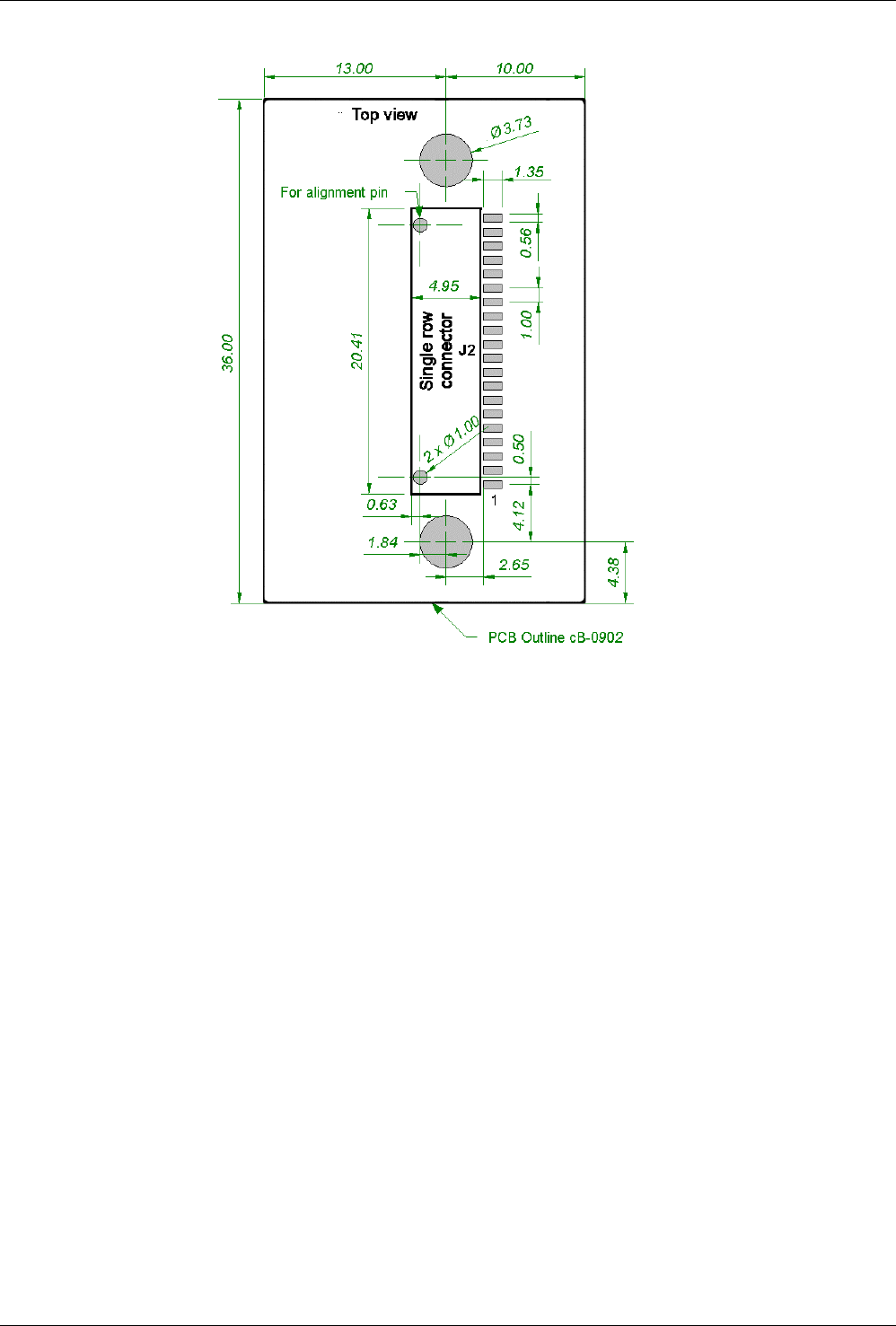
5.2.1 Suitable One-Piece Part Connectors
5.2.1.1 Single row connectors
These connectors are a single row connector and can be used if only J2 is needed.
This connector has a profile height of 1.65 mm and this has to be considered if components
are to be mounted on the motherboard under the OEM Serial Port Adapter board.
There are alignment pins on the bottom side of the connector.
The connector is available with M2 threaded inserts that fit the mounting holes on the board
(see section 5.1.2). You may screw the OEM Serial Port Adapter board directly into these
inserts. If you want to have a tighter and more secure mounting, you may use longer screws
and secure it using a nut on the backside of the motherboard.
Another way to mount the module is to use press-fit nuts on the motherboard and skip the
M2 threads on the connector, see section 5.3 for more information about press-fit nuts.
Table 14: Single row connectors from Samtec.
Samtec order
number
Quote
number
Equivalent part Package Remark
ASP-118645-01 55392 SEI-120-02-GF-S-AB Tube Align pin on bottom
side only
ASP-118645-02 55392 SEI-120-02-GF-S-AB-TR Tape-n-Reel Align pin on bottom
side only
ASP-118579-01 55392 SEI-120-02-GF-S-M-AB Tube With M2 threaded
inserts and align pin on
bottom side only
ASP-118579-02 55392 SEI-120-02-GF-S-M-AB-TR Tape-n-Reel With M2 threaded
inserts and align pin on
bottom side only
NOTE:
When ordering connectors from Samtec or an official Samtec distributor, please use the ASP
order number and refer to the connectBlue global quote number for best price. For technical
questions regarding the Samtec connectors please contact connectBlue or Samtec at
(Scandinavia@samtec.com).
See Figure 7 for more information about the connector and necessary measurements on the
motherboard. The large mounting holes on the motherboard are designed for press-fit nuts
and could be smaller if press-fit nuts are not used. The mounting holes are aligned with the
outer tangent of the 2.3mm mounting holes of the module (see section 5.1.2).
Version 1.4.1 - 2006-04 31
Figure 7: Host PCB layout [mm] for single row connector.

Version 1.4.1 - 2006-04 32
5.2.1.2 Double row connectors
This connector is a double row connector and can be used if both J2 and J3 are needed.
This connector has a height of 3.0mm and this has to be considered if components are to be
mounted on the motherboard under the OEM Serial Port Adapter board. The connector is
also available with a height of 6.0mm and 10.0mm (The FSI-120 serie from Samtec).
There are alignment pins on the bottom side of the connector.
The connector is available with M2 threaded inserts that fit the mounting holes on the board
(see section 5.1.2). You may screw the OEM Serial Port Adapter board directly into these
inserts. If you want to have a tighter and more secure mounting you may use longer screws
and secure it using a nut on the backside of the motherboard.
Another way to mount the module is to use press-fit nuts on the motherboard and skip the
M2 threads on the connector, see section 5.3 for more information about press-fit nuts.
Table 15: Double row connectors from Samtec.
Samtec order
number
Quote
number
Equivalent part Package Remark
REF-120021-01 55392 FSI-120-03-G-D-AB Tube Align pin on bottom
side only
REF-120021-02 55392 FSI-120-03-G-D-AB-K-TR Tape-n-Reel Align pin on bottom
side only
REF-120018-01 55392 FSI-120-03-G-D-M-AB Tube With M2 threaded
inserts and align pin
on bottom side only
REF-120018-02 55392 FSI-120-03-G-D-M-AB-K-TR Tape-n-Reel With M2 threaded
inserts and align pin
on bottom side only
NOTE:
When ordering connectors from Samtec or an official Samtec distributor, please use the REF
order number and refer to the connectBlue global quote number for best price. For technical
questions regarding the Samtec connectors please contact connectBlue or Samtec at
(Scandinavia@samtec.com).
See Figure 8 for more information about the connector and necessary measurements on the
motherboard. The large mounting holes on the motherboard are designed for press-fit nuts
and could be smaller if press-fit nuts are not used (see section 5.1.2).
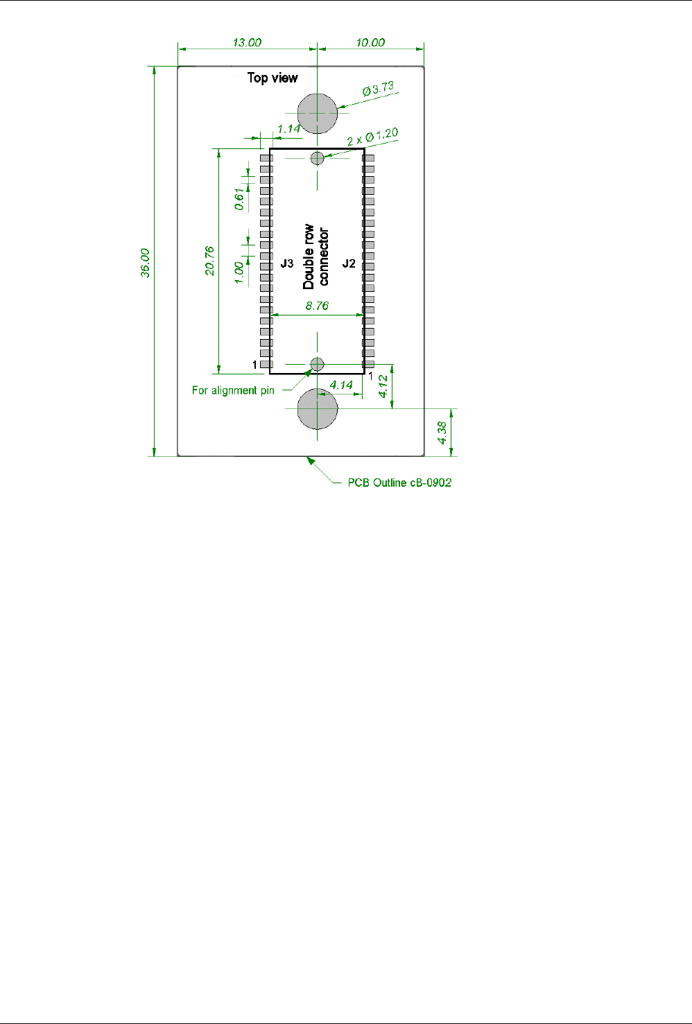
Version 1.4.1 - 2006-04 33
Figure 8: Host PCB layout [mm] for double row connector.

Version 1.4.1 - 2006-04 34
5.3 Using Press-Fit Nuts for Mounting the Module
A press-fit nut is pressed into the PCB from the bottom side with a special press tool. M2
sized press-fit nuts are suitable for the modules (see Figure 7 and Figure 8) and are
manufactured by PEM Fastening Systems (www.pemnet.com), part no KFS2-M2 (see Figure
9). Be careful with the distance between the nuts regarding alignment, see section 5.1.2.
Figure 9: KFS2-M2 press-fit nut.
Spacer-pipes are recommended to use between the PCBs when press-fit nuts are used.
5.4 Antenna Issues
The unit cannot be mounted arbitrary, because of the radio communication. The unit with an
internal surface mounted antenna (CB-OEMSPA312i and CB-OEMSPA332i) cannot be
mounted in a metal enclosure.
No metal casing or plastics using metal flakes should be used, avoid also metallic based
paint or lacquer. Keep a minimum clearance of 10mm between the antenna and the casing.
Keep 10 mm free space from metal around the antenna.
If a metal enclosure is required, one of the external antenna options has to be used. See
section 4.2 for more information on the antenna options available.

Version 1.4.1 - 2006-04 35
6 Bluetooth Information
6.1 General information
In the tables below you can find information about Bluetooth properties. The cB-0902 module
is available in two output power versions both Bluetooth Class 1. The output power of the
cB-OEMSPA312i/x device is max +7dBm (5mW) and the output power of the cB-
OEMSPA332i/x device is max +16.9dBm (49mW).
Table 16: Bluetooth information CB-OEMSPA-312i/x
Parameter Data
Bluetooth radio Philips BGB203
Bluetooth base band controller Philips BGB203
RF output power Class 1, max 7dBm (5mW)
Receive sensitive level -90dBm
Receive input level (max) +15dBm
Output frequency 2.402 –2.480 GHz, ISM band.
Bluetooth stack Embedded host stack
Bluetooth qualification 2.0
Table 17: Bluetooth information CB-OEMSPA-332i/x
Parameter Data
Bluetooth radio Phillips BGB203
Bluetooth base band controller Phillips BGB203
Radio power amplifier muRata MF2400PS-AL0909 (+20dB)
RF output power Class 1, max 16.9dBm (49mW)
Receive sensitive level -89dBm
Receive input level (max) +16dBm
Output frequency 2.402 –2.480 GHz, ISM band.
Bluetooth stack Embedded host stack
Bluetooth qualification 2.0

Version 1.4.1 - 2006-04 36
6.2 Bluetooth Qualification information
All products based on the PCB cB-0902-02 have been qualified according to the Bluetooth
specification 2.0.
Table 18 - Bluetooth Qualification information
Module Bluetooth specification QPLN reference Qualification date
cB-OEMSPA312i /x 2.0 B02690 2005-11-15
cB-OEMSPA332i/x 2.0 B02993 2006-03-17
The following Bluetooth profiles are supported (covered functionality):
• Generic Access Profile (GAP)
• Serial Port Profile (SPP)
• Dial-up Networking Profile (DUN GW, DUN DT)
When creating end products based on the Serial Port Adapter the following applies:
• The end product does not have to be re-qualified.
• The end product or the end product documentation based on:
o cB-OEMSPA312i /x products shall make the following information available:
“This product contains a Bluetooth qualified product QPLN B02690”.
o cB-OEMSPA332i /x products shall make the following information available:
“This product contains a Bluetooth qualified product QPLN B02993”.
• The Bluetooth Trademark may be placed on the end product (requires Bluetooth SIG
membership, for more information see www.bluetooth.org).
• The Bluetooth Trademark may be used in material related to the end product (requires
Bluetooth SIG membership, for more information see www.bluetooth.org).
For more information please contact connectBlue.

Version 1.4.1 - 2006-04 37
7 Regulatory Information
7.1 Declaration of Conformity
We, connectBlue AB, of
Norra Vallgatan 64 3V
SE-211 22 Malmö, Sweden
declare under our sole responsibility that our products:
cB-OEMSPA312i/x (cB-0069, cB-0070, cB-0071, cB-0072, cB-0073, cB-0074, cB-0075, cB-0076),
cB-OEMSPA332i/x (cB-0077, cB-0078, cB-0079, cB-0080, cB-0081, cB-0082, cB-0083, cB-0084),
OEM Module Adapter III (cB-0068).
to which this declaration relates, conforms to the following product specifications:
R&TTE Directive 1999/5/EC
EN 300 328 V1.6.1 (2004-11)
EMC Directive: 89/336/EEC
EN 301 489-1 V1.4.1 (2002-08)
EN 301 489-17 V1.2.1 (2002-08)
EN 61000-6-2 (2001)
Safety Compliance
EN 60950-1:2001 and/or IEC 60950-1:2001 (1st Edition)
EN 60950-1/A11:2004 + Corrigendum:2004
Medical Electrical Equipment
IEC 60601-1-2 (2001)
18/11/2005 Malmö, Sweden
Mats Andersson
CTO of connectBlue AB
If a cB-OEMSPA332i/x is used within EU a notification must be made to each of the national
authorities responsible for radio spectrum management of the intention to place radio
equipment that uses frequency bands whose use is not harmonized throughout the EU, on
its national market.
More information at: http://europa.eu.int/comm/enterprise/rtte/gener.htm

Version 1.4.1 - 2006-04 38
7.2 Safety Compliance
In order to fulfill the safety standard EN 60950-1 the unit must be supplied by a limited power
source.
7.3 FCC and IC Compliance
See Table 1 for information about the different product variants.
7.3.1 Compliance for cB-0902-0201
7.3.1.1 FCC Statement for cB-0902-0201
This device complies with Part 15 of the FCC Rules. Operation is subject to the following two
conditions: (1) this device may not cause harmful interference, and (2) this device must
accept any interference received, including interference that may cause undesired operation.
NOTE: This equipment has been tested and found to comply with the limits for a Class B
digital device, pursuant to Part 15 of the FCC Rules. These limits are designed to provide
reasonable protection against harmful interference in a residential installation. This
equipment generates, uses and can radiate radio frequency energy and, if not installed and
used in accordance with the instructions, may cause harmful interference to radio
communications. However, there is no guarantee that interference will not occur in a
particular installation. If this equipment does cause harmful interference to radio or television
reception, which can be determined by turning the equipment off and on, the user is
encouraged to try to correct the interference by one or more of the following measures:
• Reorient or relocate the receiving antenna
• Increase the separation between the equipment and receiver
• Connect the equipment into an outlet on a circuit different from that to which the
receiver is connected
Consult the dealer or an experienced radio/TV technician for help
7.3.1.1.1 Antenna
Our module type cB-0902-0201 is for OEM integrations only. The end-user product will be
professionally installed in such a manner that only the authorized antennas are used.
7.3.1.1.2 Caution
Any changes or modifications NOT explicitly APPROVED by connectBlue AB could cause
the module to cease to comply with FCC rules part 15, and thus void the user’s authority to
operate the equipment.
7.3.1.2 IC Compliance
Operation is subject to the following two conditions:
(1) this device may not cause harmful interference, and
(2) this device must accept any interference received,
including interference that may cause undesired operation.
This device has been designed to operate with an antenna having a maximum gain of 2.7
dBi.
Having a higher gain is strictly prohibited per regulations of Industry Canada. The required
antenna impedance is 50 ohms.
To reduce potential radio interference to other users, the antenna type and its gain should be
so chosen that the equivalent isotropically radiated power (EIRP) is not more than that
required for successful communication.

Version 1.4.1 - 2006-04 39
The installer of this radio equipment must ensure that the antenna is located or pointed such
that it does not emit RF field in excess of Health Canada limits for the general population;
consult Safety Code 6, obtainable from Health Canada’s website www.hc-sc.gc.ca/rpb
7.3.1.3 Labeling Requirements for End Product
For an end product using the product cB-0902-0201 there must be a label containing, at
least, the following information:
The label must be affixed on an exterior surface of the end product such that it will be visible
upon inspection in compliance with the modular approval guidelines developed by the FCC.
Where the module will be installed in final products larger than 8 cm x 10 cm following
statement has to be placed ONTO the device.
“This device complies with Part 15 of the FCC Rules.
Operation is subject to the following two conditions:
(1) this device may not cause harmful interference, and
(2) this device must accept any interference received, including interference that may cause
undesired operation.”
In case, where the final product will be installed in locations where the end-consumer is not
able to see the FCC ID and/or this statement, the FCC ID and the statement shall also be
included in the end-product manual.
This device contains
FCC ID: PVH090202S
IC: 5325A-090202S

Version 1.4.1 - 2006-04 40
7.3.2 Compliance for cB-0902-0202
7.3.2.1 FCC Statement for cB-0902-0202
This device complies with Part 15 of the FCC Rules. Operation is subject to the following two
conditions: (1) this device may not cause harmful interference, and (2) this device must
accept any interference received, including interference that may cause undesired operation.
NOTE: This equipment has been tested and found to comply with the limits for a Class B
digital device, pursuant to Part 15 of the FCC Rules. These limits are designed to provide
reasonable protection against harmful interference in a residential installation. This
equipment generates, uses and can radiate radio frequency energy and, if not installed and
used in accordance with the instructions, may cause harmful interference to radio
communications. However, there is no guarantee that interference will not occur in a
particular installation. If this equipment does cause harmful interference to radio or television
reception, which can be determined by turning the equipment off and on, the user is
encouraged to try to correct the interference by one or more of the following measures:
• Reorient or relocate the receiving antenna
• Increase the separation between the equipment and receiver
• Connect the equipment into an outlet on a circuit different from that to which the
receiver is connected
Consult the dealer or an experienced radio/TV technician for help
7.3.2.1.1 Antenna
Our module type cB-0902-0202 is for OEM integrations only. The end-user product will be
professionally installed in such a manner that only the authorized antennas are used.
7.3.2.1.2 Caution
Any changes or modifications NOT explicitly APPROVED by connectBlue AB could cause
the module to cease to comply with FCC rules part 15, and thus void the user’s authority to
operate the equipment.
7.3.2.2 IC Compliance
Operation is subject to the following two conditions:
(1) this device may not cause harmful interference, and
(2) this device must accept any interference received,
including interference that may cause undesired operation.
This device has been designed to operate with an antenna having a maximum gain of 8dBi.
Having a higher gain is strictly prohibited per regulations of Industry Canada. The required
antenna impedance is 50 ohms.
To reduce potential radio interference to other users, the antenna type and its gain should be
so chosen that the equivalent isotropically radiated power (EIRP) is not more than that
required for successful communication.
The installer of this radio equipment must ensure that the antenna is located or pointed such
that it does not emit RF field in excess of Health Canada limits for the general population;
consult Safety Code 6, obtainable from Health Canada’s website www.hc-sc.gc.ca/rpb.

Version 1.4.1 - 2006-04 41
7.3.2.3 Labeling Requirements for End Product
For an end product using the product cB-0902-0202 there must be a label containing, at
least, the following information:
The label must be affixed on an exterior surface of the end product such that it will be visible
upon inspection in compliance with the modular approval guidelines developed by the FCC.
Where the module will be installed in final products larger than 8 cm x 10 cm following
statement has to be placed ONTO the device.
“This device complies with Part 15 of the FCC Rules.
Operation is subject to the following two conditions:
(1) this device may not cause harmful interference, and
(2) this device must accept any interference received, including interference that may cause
undesired operation.”
In case, where the final product will be installed in locations where the end-consumer is not
able to see the FCC ID and/or this statement, the FCC ID and the statement shall also be
included in the end-product manual.
7.3.2.4 RF-exposure Statement for cB-0902-0202
This modular transmitter MUST have a separation distance of at least 20 cm between the
antenna and the body of the user or nearby persons, excluding hands, wrists, feet, and
ankles.
If the radio module is installed in a laptop display, transmission MUST be prevented if the lid
is closed to ensure that the minimum distance of 20 cm between the user and the
transmitting antenna is maintained.
Any notification to the end user of installation or removal instructions about the integrated
radio module is NOT allowed.
This device contains
FCC ID: PVH090202L
IC: 5325A-090202L

Version 1.4.1 - 2006-04 42
7.4 UL listing information
If a customer intends to UL list a product including any of the Bluetooth modules based on
the PCB cB-0902-02 this information is useful:
The printed circuit board if produced according to the following specification:
• UL recognized ZPMV2 min. 105 °C flame class V-0 or better.
7.5 Compliance with RoHS directive
All products based on the PCB cB-0902-02 are produced according to the RoHS (Restriction
of the use of certain Hazardous substances in electrical and electronic equipment) directive
and complies with the directive.

Version 1.4.1 - 2006-04 43
8 Guidelines for Efficient and Safe Use
8.1 General
Read this information before using your OEM Serial Port Adapter.
For any exceptions, due to national requirements or limitations, when using your OEM Serial
Port Adapter, please visit www.bluetooth.org.
Note: Changes or modifications to the product not expressly approved by
connectBlue AB will void the user’s authority to operate the equipment.
8.2 Product Care
• Do not expose your product to liquid or moisture.
• Do not expose you product to extreme hot or cold temperature (see Section 2.3.3 for
further information)
• Do not expose your product to lit candles, cigarettes, cigars, open flames, etc.
• Do not drop, throw or try to bend your product since rough treatment could damage your
product.
• Do not attempt to disassemble your product. Doing so will void warranty. The product
does not contain consumer serviceable or replaceable components. Service should only
be performed by connectBlue AB.
• Do not paint your product as the paint could prevent normal use.
• If you will not be using your product for a while, store it in a place that is dry, free from
damp, dust and extreme heat and cold.
8.3 Radio Frequency Exposure
The OEM Serial Port Adapter contains a small radio transmitter and receiver. During
communication with other Bluetooth products the OEM Serial Port Adapter receives and
transmits radio frequency (RF) electromagnetic fields (microwaves) in the frequency range
2400 to 2500 MHz. The output power of the radio transmitter is very low.
When using the OEM Serial Port Adapter, you will be exposed to some of the transmitted RF
energy. This exposure is well below the prescribed limits in all national and international RF
safety standards and regulations.

Version 1.4.1 - 2006-04 44
8.4 Electronic Equipment
Most modern electronic equipment, for example, in hospitals and cars, is shielded from RF
energy. However, certain electronic equipment is not. Therefore:
Note: This equipment emits RF energy in the ISM (Industrial, Scientific, Medical) band.
Please insure that all medical devices used in proximity to this device meet appropriate
susceptibility specifications for this type of RF energy.
8.5 Potentially Explosive Atmospheres
Turn off your electronic device before entering an area with potentially explosive
atmosphere. It is rare, but your electronic device could generate sparks. Sparks in such
areas could cause an explosion or fire resulting in bodily injury or even death.
Areas with a potentially explosive atmosphere are often, but not always, clearly marked.
They include fuelling areas, such as petrol station, below deck on boats, fuel or chemical
transfer or storage facilities, and areas where the air contains chemicals or particles, such as
grain, dust, or metal powders.
8.6 Power Supply
The OEM Serial Port Adapter must be supplied by a limited power source according to
EN 60950-1.
• Connect your power supply only to designated power-sources as marked on the
product.
• Make sure all cords and cable are positioned so that they will not be stepped on, tripped
over or otherwise subject to damage or stress.
• To reduce risk of electric shock, unplug the unit from any power source before
attempting to clean it.

Version 1.4.1 - 2006-04 45
Appendix A - Application Notes
Usually only a subset of the available functionality is of interest to the designer. In addition,
depending on the host system, the electrical interface can be designed in many ways. The
designer can use the step-by-step guide in this chapter as an aid in the design process.
A.1 Step-by-Step Guide
Table 19: Step-by-step guide with Yes and No answers.
Question Yes No
Are you going to integrate the OEM
Serial Port Adapter in a metal enclo-
sure?
The internal antenna models
cannot be used. Use the OEM-
SPA312x or OEMSPA332x.
You are free to choose
between the products. The
internal antenna models
are lower cost and are
easier to design-in. How-
ever, an external antenna
could give better range.
Do you wish to use logic level when
communicating with the OEM Serial
Port Adapter?
See section A.2.2.1 for electrical
design.
Go on to next point.
Do you want to use RS232 as the
physical serial interface?
See section A.2.2.2 for electrical
design.
Go on to next point.
Do you want to use RS485 or RS422
as the physical serial interface?
See section A.2.2.3 - A.2.2.4 for
electrical design.
Go on to next point.
Are you using a 5V host system? See section A.2.1, Figure 11 for
electrical design.
See section A.2.1, Figure
10 for electrical design.
Is low power consumption important? The power consumption can be
reduced by enabling the stop
mode, see Table 9. The stop
mode is controlled with the DSR
pin, see section 2.5. The power
consumption is optimized with
3.2-3.3 V supply voltage.
Go on to next point.
Do you wish to connect LEDs to the
OEM Serial Port Adapter?
See section A.2.3 for design
examples for connecting the
LEDs.
Go on to next point.
Do you want to detect the status of
the module with a controller?
See Chapter 3, Table 13 for
status detection and section A.2.3
for electrical design.
Go on to next point.
Do you wish to utilize the restore
switch?
See section A.2.3.3 for electrical
design.
Go on to next point.
Do you wish to utilize the Function
switch (“Connect on external sig-
nal”)?
See section A.2.3.4 for electrical
design.
Go on to next point.
Do you want to manually reset the
module?
See section A.2.4 for electrical
design. Use a double row con-
nector. See section 5.2.1.2.
Version 1.4.1 - 2006-04 46
A.2 Design Examples
This section contains design examples for all interfaces on J1, J2, J3, J7 and J8. The
connector type that suits a specific application depends on the needed signal and the
preferred interface type (wires, flexfilm, board-to-board or SMD).
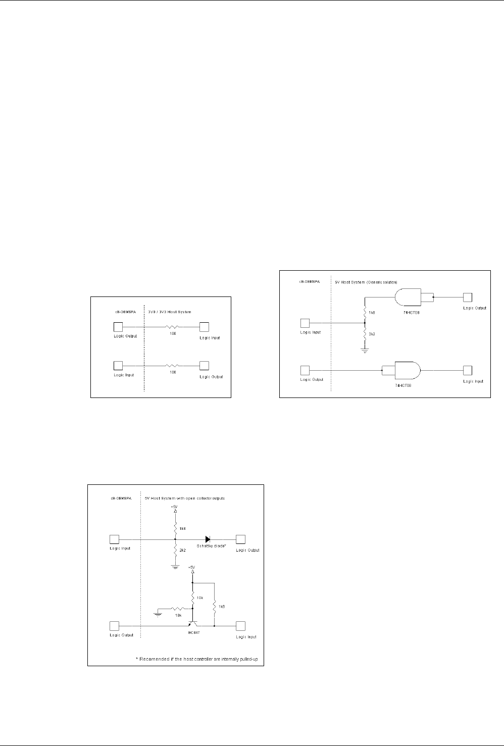
A.2.1 Logic Levels
A 3.0/3.3V host system can be connected directly to the logic level pins (BLUE, UART-TxD /
UART-RxD etc). A serial 100Ω resistor shall be used (see Figure 10) for protection, see
Table 11 for logic levels characteristics.
A 5V host system can easily be adjusted to the logic levels. A host system output signal can
use a resistive divider (18k/22k) to adjust the levels. This is applicable for speeds up to
115.2kBits/s. The divider can be adjusted to 1.8k/2.2k and a logic buffer (74HCT08) for
higher speeds (see Figure 11). The host system input pins could require a buffer (see Figure
11) depending on the logic level requirements (see Table 11).
The 74HCT08 gate is also available in a single gate package (74AHCT1G08).
Figure 10: Logic levels interface to a 3/3.3V
system. A protective 100Ω
ΩΩ
Ω resistor is used.
Figure 11: Interface example with logic levels to a 5V
system.
A 5V system with open collector outputs is designed in Figure 12.
Figure 12: Open collector outputs.
Version 1.4.1 - 2006-04 47
A.2.2 Serial Interface
The serial interface can operate in RS232 or Logic level mode, see section A.2.3.2.
The Logic level mode could be used if the module is connected to an external CPU or if the
physical interface should be another then the internal RS232 likes RS422 (see section
A.2.2.3).
The signal excluding the RxD and TxD signals available on the serial interface are:
CTS (Clear To Send) and RTS (Request To Send) are used for hardware flow control.
DSR (Data Set Ready) can be used to make a connect attempt. See the Serial Port Adapter
AT commands specification.
DTR (Data Terminal Ready) can be used to detect if the module is up and running and ready
to receive data.
Note! The module must be configured to flow control none if hardware flow control is
not used, see the Serial Port Adapter AT Commands document.
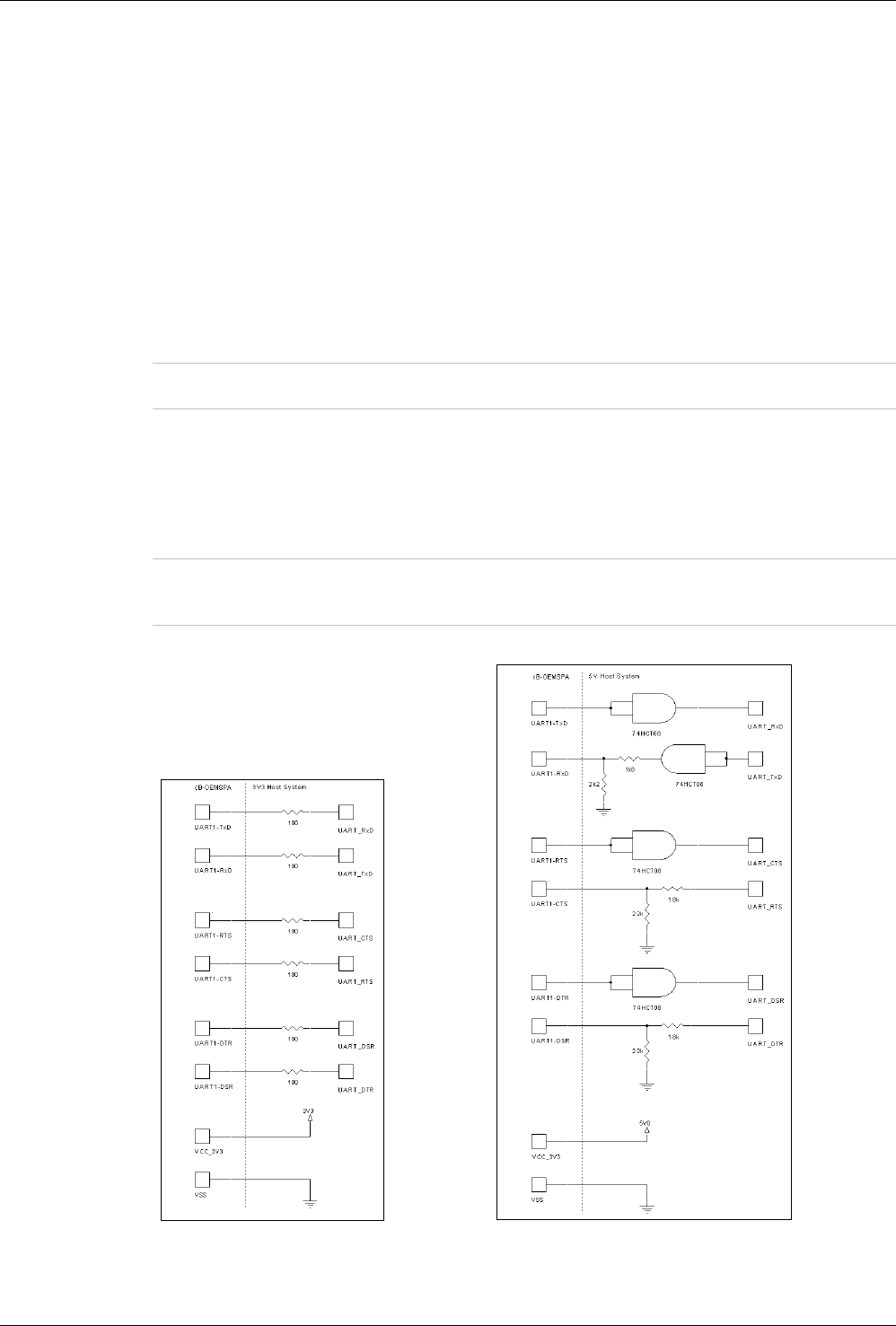
A.2.2.1 Logic level Mode
The serial UART interface can be used in a host controller application with a UART interface.
The design of the interface depends on the power supply voltage of the host system; see
Figure 13 for a 3.0/3.3V host system and Figure 14 for a 5V host system.
See section A.2.3.2 for information on how to select Logic level mode.
Note! It is very important to set the module in logic level mode properly when
interfacing with logic levels; collision with the internal RS232 transceiver could
damage the module.
Figure 13: A complete UART interface with a
3.0/3.3V host system.
Figure 14: A complete UART interface with a
5V host system.
Version 1.4.1 - 2006-04 48
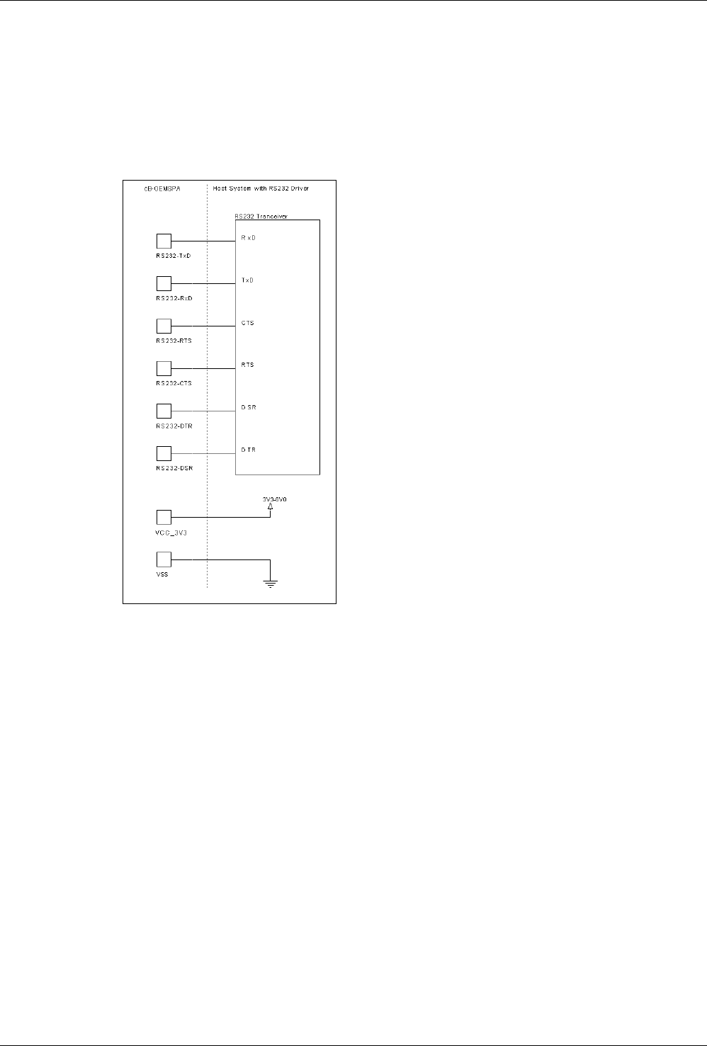
A.2.2.2 External RS232 driver
The modules are fully compatible with the EIA-232 standard and can be connected to all
RS232 transceivers. Speed and current consumption depends on the host system RS232
transceiver. See Figure 15 for a complete example. Not used functionality can be left
unconnected; see Section A.2.2.
Figure 15: A complete RS232 interface.
Version 1.4.1 - 2006-04 49
A.2.2.3 External RS422 transceiver
An external RS422 driver could be used in a point-to-point (full duplex) application (see
Figure 16).
The Logic level mode needs to be enabled when using an external transceiver. See section
A.2.3.2 for information on how to select Logic level mode.
Note! It is very important to set the module in logic level mode properly when
interfacing with logic levels; collision with the internal RS232 transceiver could
damage the module.
Figure 16: A complete RS422 interface.
Version 1.4.1 - 2006-04 50
A.2.2.4 External RS422/RS485 transceiver
A complete RS422/RS485 transceiver design connected to a bus system need to control the
enable signals of the transceiver. The SerialSelect signals are used for this purpose (see
Table 20).
The Logic level mode needs to be enabled when using an external transceiver. See section
A.2.3.2 for information on how to select Logic level mode. The module need also to be
software configured to the corrected interface, see the Serial Port Adapter AT Commands
document how to configure the module to the correct serial interface.
Table 20: SerialSelect signals combinations
Serial
Select-0
Serial
Select-1
Internal RS232
Transceiver status
RS485/RS422 Transmitter
status (Active high)
RS485/RS422 Receiver
status (Active low)
0 0 Disabled Disabled Enabled
0 1 Disabled Enabled Enabled
1 0 Disabled Enabled Disabled
1 1 Enabled Disabled Disabled
Note! It is very important to set the module in logic level mode properly when
interfacing with logic levels; collision with the internal RS232 transceiver could
damage the module.
Figure 17: A complete RS422/RS488 transceiver design.
Version 1.4.1 - 2006-04 51
A.2.3 LED and Switch Design
A.2.3.1 BLUE Signal
The BLUE logic LED signal is not multiplexed with any other functionality, which makes the
design more straightforward (for more information see Figure 18). There are two important
notes:
- A blue LED requires about 3.5V forward voltage drop (cannot be used in a 3.3V
system).
- The BLUE signal can be used to detect if the module is connected or not. The BLUE
signal flashes when the module is sending and receiving data (see Chapter 3, Table
13). See Figure 19 for an example on how to suppress the flashes.
Figure 18: A blue LED can be connected directly to the module if the LED current is below 4mA. A high
state (active low) makes the voltage drop over the LED to 2.2V. This is not enough to light the LED.
Figure 19: A Low pass filter and a 74HC08 suppress the flashes when the module is sending and receiving
data. The Blue LED can be removed if not required. The values are not suited in all applications and need to
be verified in a specific application.
Version 1.4.1 - 2006-04 52
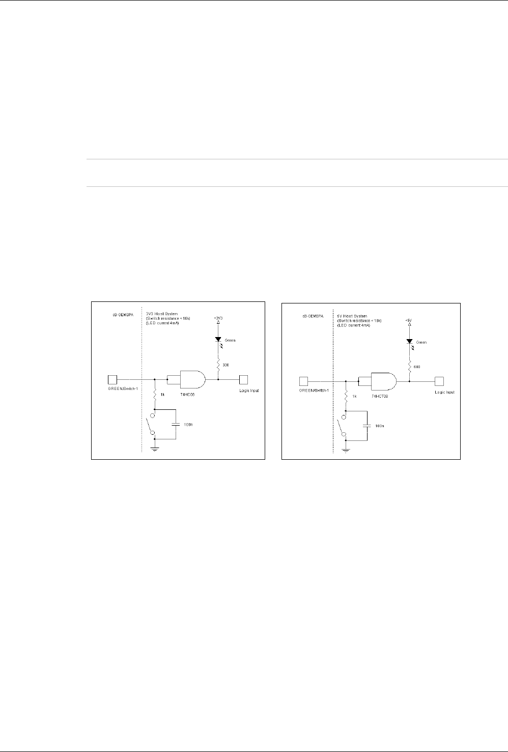
A.2.3.2 RED/Mode Signal
The RED/Mode signal is a multiplexed signal:
- RED - Logic red LED signal (see Chapter 3, Table 13). Becomes valid 500ms after start
up.
- Mode - The module reads the status of the signal during startup to decide if the serial
interface shall be RS232 (HIGH) or logic UART (LOW) levels. The input signal must be
stable for the first 500ms after startup (after reset/power on reset).
The signal is internally pulled-up (16kΩ) for RS232 as default.
Note! The internal 16k
Ω
ΩΩ
Ω
pull-up is smaller than on previous product generations from
connectBlue. This requires a smaller pull-down resistor (1k
Ω
ΩΩ
Ω
) for a low state.
If a LED is used in UART mode a high impendence buffer is required to prevent the signal
from being pulled-up via the LED. A 74HC08 logic gate can be used in a 3/3.3V system (see
Figure 20) and a 74HCT08 logic gate in a 5V system (see Figure 21). Both gates are
available in a single gate package (74AHC1G08/74AHCT1G08).
Figure 20: UART mode selected together with
a red LED in a 3.3V host system. The status of
the signal can also be used as input to a host
controller.
Figure 21: UART mode selected together with
a red LED in a 5V host system. The status of
the signal can also be used as input to a host
controller.
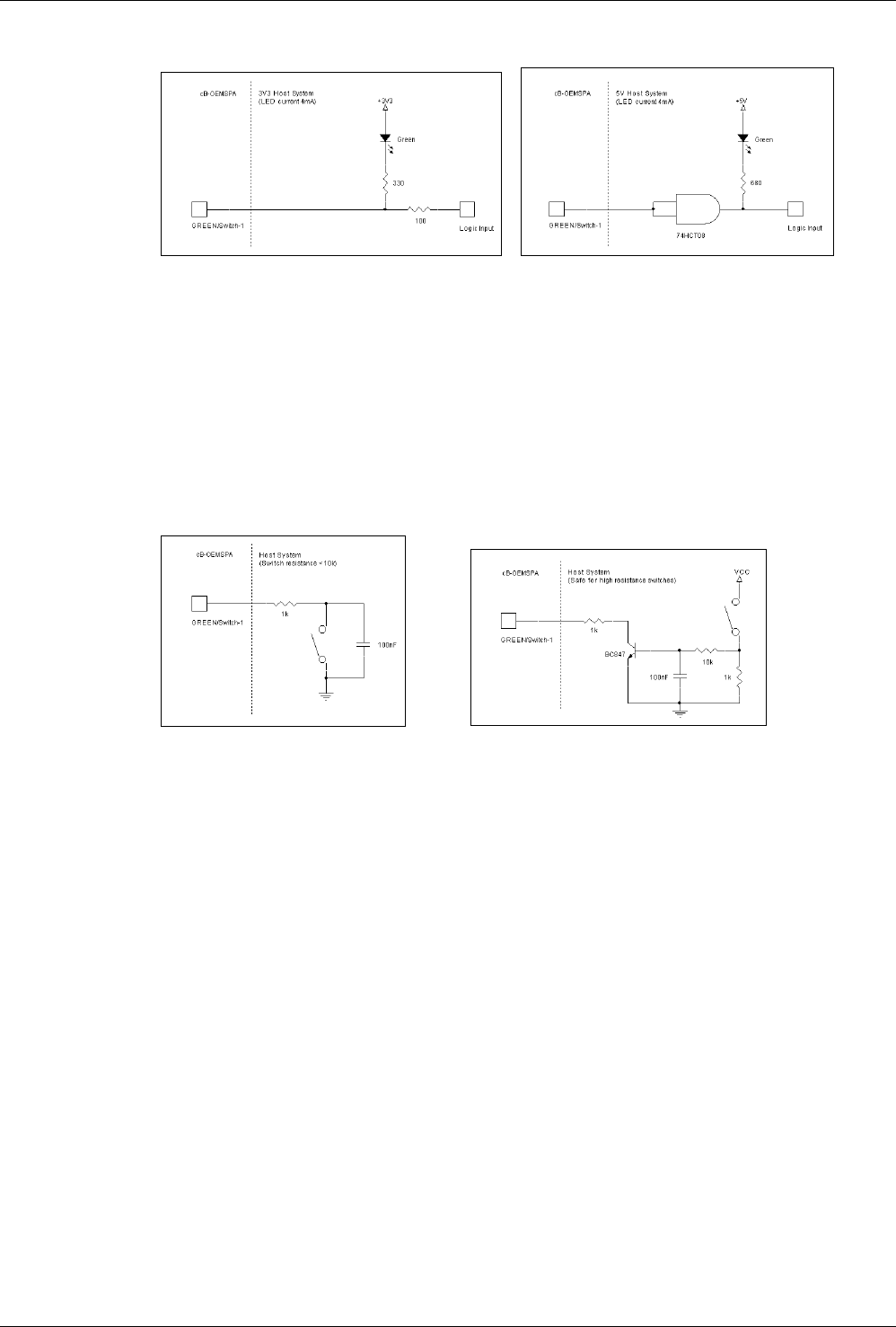
The buffer can be removed in a 3.3V system if RS232 mode is used (see Figure 22).
In a 5V system the high state output (2.8V) from the module is not enough to turn off the
LED so a 74HCT08 buffer can be used to raise the high level to 5V (see Figure 23).
The 74HCT08 gate is available in a single gate package (74AHCT1G08).
Figure 22: RS232 mode selected (default) together
with a red LED in a 3.3V host system. The status of
the signal can also be used as input to a host con-
troller.
Figure 23: RS232 mode selected (default)
together with a red LED in a 5V host system.
The status of the signal can also be used as
input to a host controller.
Only a pull-down on the RED/Mode pin is needed if UART mode is used but no red LED is
required (see Figure 24). The RED/Mode pin can be left unconnected if RS232 (default) is
used and no red LED required.

Version 1.4.1 - 2006-04 53
Figure 24: The mode pin is pulled-down (1kΩ
ΩΩ
Ω) in UART mode.
Version 1.4.1 - 2006-04 54
A.2.3.3 GREEN/Switch-1 signal
The GREEN/Switch-1 signal is a multiplexed signal:
- GREEN - Logic green LED signal (see Chapter 3, Table 13). Becomes valid 500ms
after start up.
- Switch-1 - The module reads the status of the signal at startup to decide if the serial
interface settings shall be restored (LOW) (see the Serial Port Adapter User Manual for
more details). The input signal must be stable for the first 500ms after startup (after
reset/power on reset).
The signal is internally pulled-up (16kΩ) to 3.0V for NOT restoring settings to default.
Note! The internal 16k
Ω
ΩΩ
Ω
pull-up is smaller than on previous product generations from
connectBlue. This requires a smaller pull-down resistor (1k
Ω
ΩΩ
Ω
) for a low state.
If a LED is used and a switch is required to be able to restore the settings, a high
impendence buffer need to prevent the signal from being pulled-up via the LED. A 74HC08
logic gate can be used in a 3/3.3V system (see Figure 25) and a 74HCT08 logic gate in a 5V
system (see Figure 26).
Both gates are available in a single gate package (74AHC1G08/74AHCT1G08).
Sometimes, over time, switch contacts can get an oxide layer. This may cause the closed
switch resistance to become too high to sink the signal to logic LOW (the signal is internally
pulled-up to 16kΩ). A design that prevents this can be found in Figure 30.
Figure 25: Switch-1 used together with a
green LED in a 3.3V host system. The status
of the signal can also be used as input to a
host controller. Notice the 1kΩ
ΩΩ
Ω serial resistor.
Figure 26: Switch-1 used together with a green
LED in a 5V host system. The status of the
signal can also be used as input to a host
controller. Notice the 1kΩ
ΩΩ
Ω serial resistor.
The buffer can be removed in a 3.3V system if no restore switch is required (see Figure 27).
In a 5V system the high state output (2.8V) from the module is not enough to turn off the
LED, so a 74HCT08 buffer can be used to raise the high level to 5V (see Figure 28).
The 74HCT08 gate is also available in a single gate package (74AHCT1G08).
Version 1.4.1 - 2006-04 55
Figure 27: No restore switch used but a green
LED in a 3.3V host system. The status of the
signal can also be used as input to a host
controller.
Figure 28: No restore switch used but a green
LED in a 5V host system. The status of the
signal can also be used as input to a host
controller.
A serial resistor to the restore switch must be used to prevent a short circuit when the
GREEN/Switch-1 pin is in output HIGH state and the switch is pressed (see Figure 29).
Sometimes, over time, switch contacts can get an oxide layer. This may cause the closed
switch resistance to become too high to sink the signal to logic LOW (the signal is internally
pulled-up to 16kΩ). A design that prevents this can be found in Figure 30.
The GREEN/Switch-1 pin can be left unconnected if none of its functionality is required.
Figure 29: A low resistance restore
switch used. Notice the 1kΩ
ΩΩ
Ω serial resis-
tor.
Figure 30: If the resistance in the switch is not
guaranteed to be low enough, a safer design can
be used. Notice the 1kΩ
ΩΩ
Ω serial resistor.
Version 1.4.1 - 2006-04 56
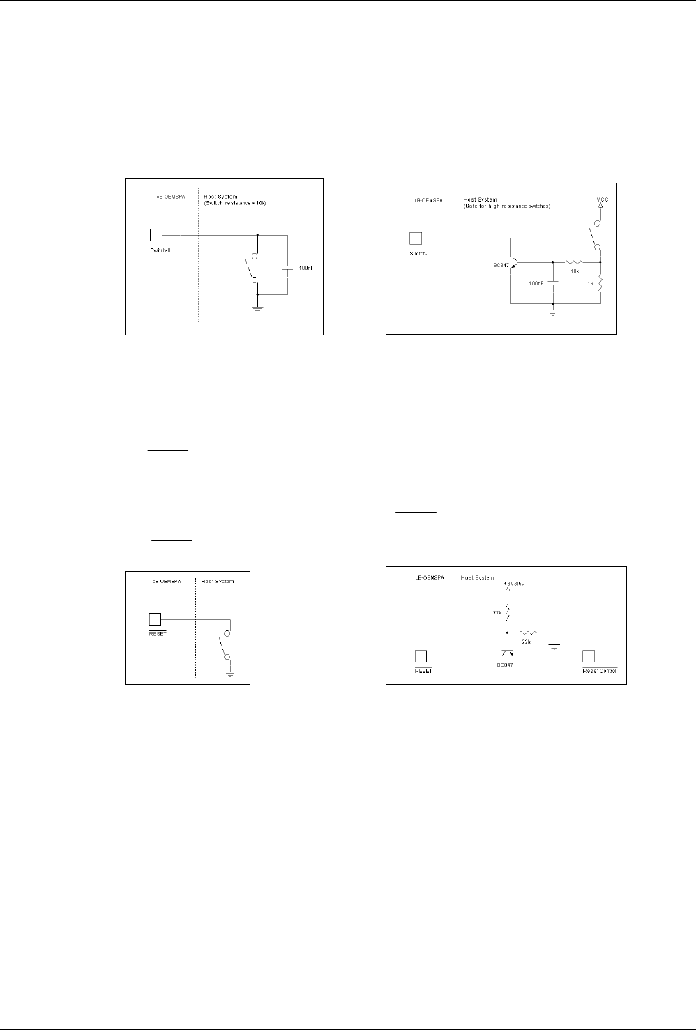
A.2.3.4 Switch-0 Signal
Switch-0 is not multiplexed with other functionality and a switch is easily implemented (see
Figure 31).
Sometimes, over time, switch contacts can get an oxide layer. This may cause the closed
switch resistance to become too high to sink the signal to logic LOW (the signal is internally
pulled-up to 16kΩ). A design that prevents this can be found in Figure 32.
The Switch-0 pin can be left unconnected if its functionality is not used.
Figure 31: A low resistance function switch
used.
Figure 32: If the resistance in the switch is not
guaranteed to be low enough, a safer design
can be used.
A.2.4 Reset
TheRESET pin can be connected to an external reset source, see Figure 33 for a switch
example.
If the reset signal is connected to an output signal it must be an open drain collector, see
Figure 34. Notice the capacitive load on the RESET pin in Table 11, section 2.3.
The RESET pin can be left unconnected if not used.
Figure 33: A reset switch. Figure 34: Design of an open collector reset
from an active high output.
Version 1.4.1 - 2006-04 57
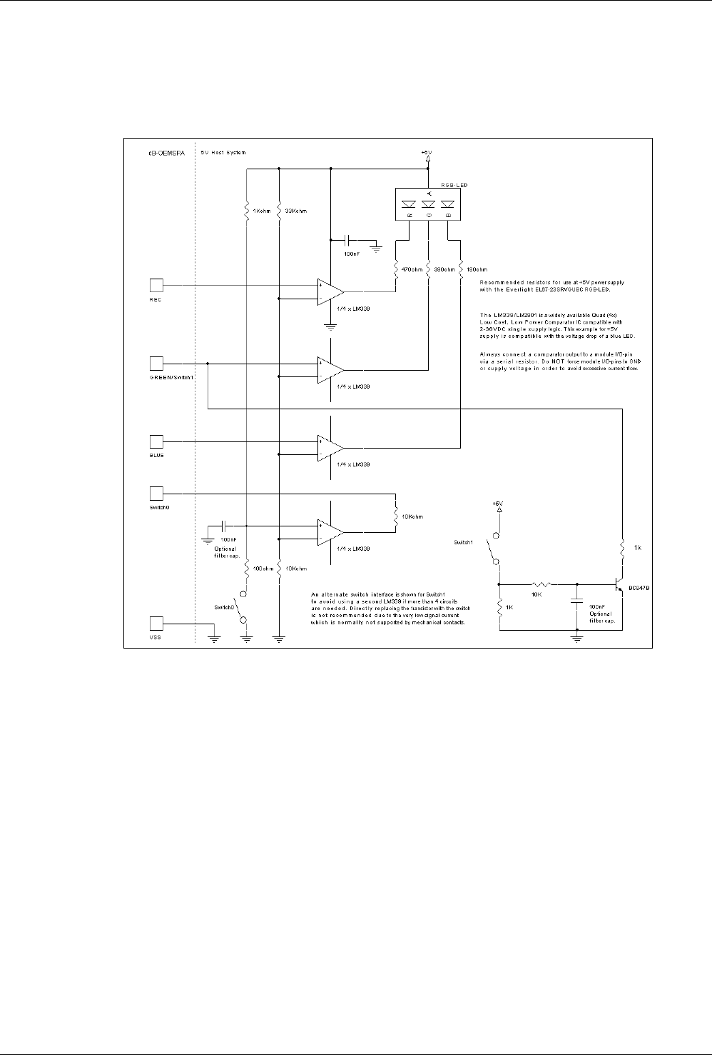
A.2.5 A Complete 5V Host System Interface
This is a complete 5V host system interface example with an RGB LED and two switches
(except the serial interface, see section A.2.2 for information). The design is based on the
LM339 Quad OP-amp instead of logic gates.
Figure 35: A complete 5V host interface with operational amplifier