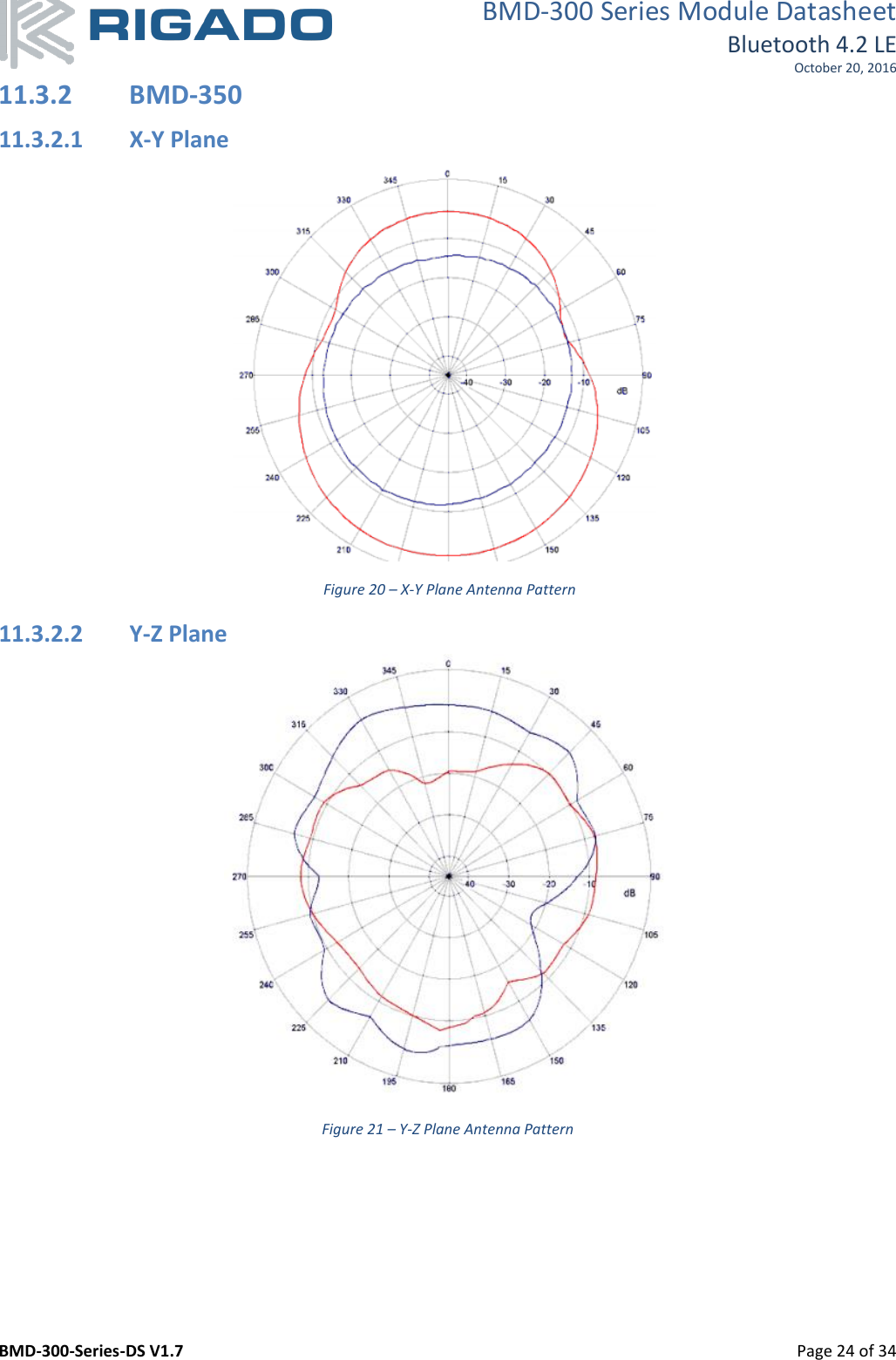
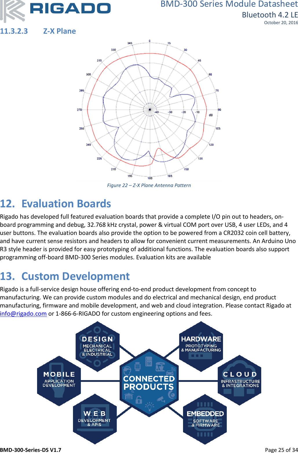
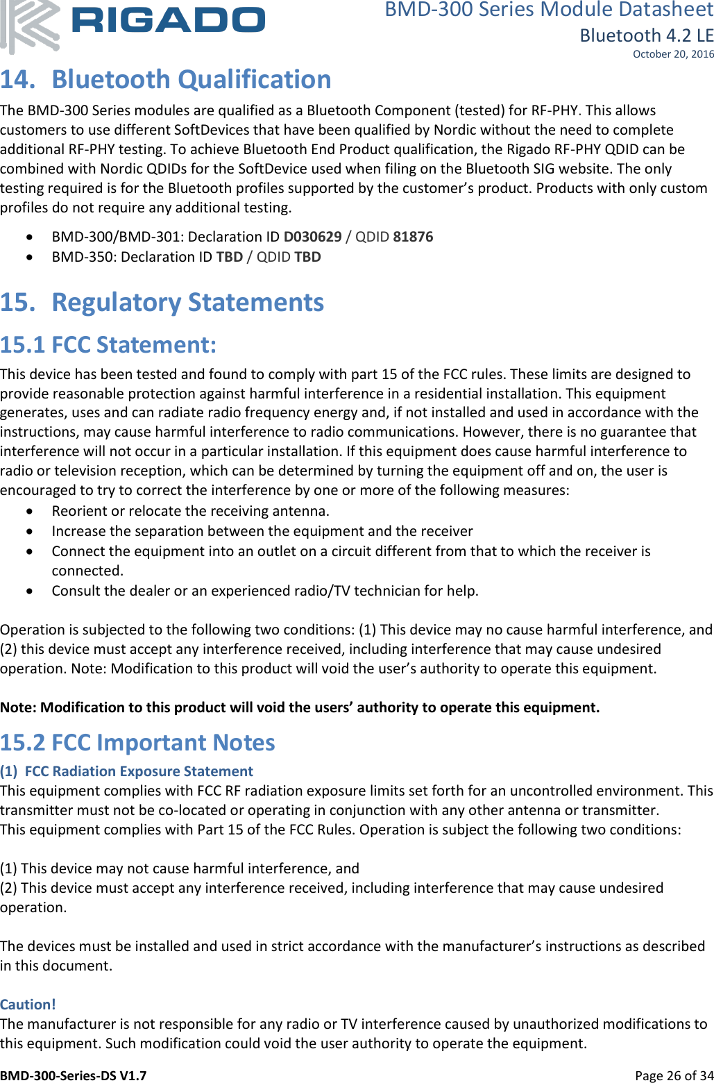
u blox 05 BMD-350 User Manual BMD 300 Series Datasheet
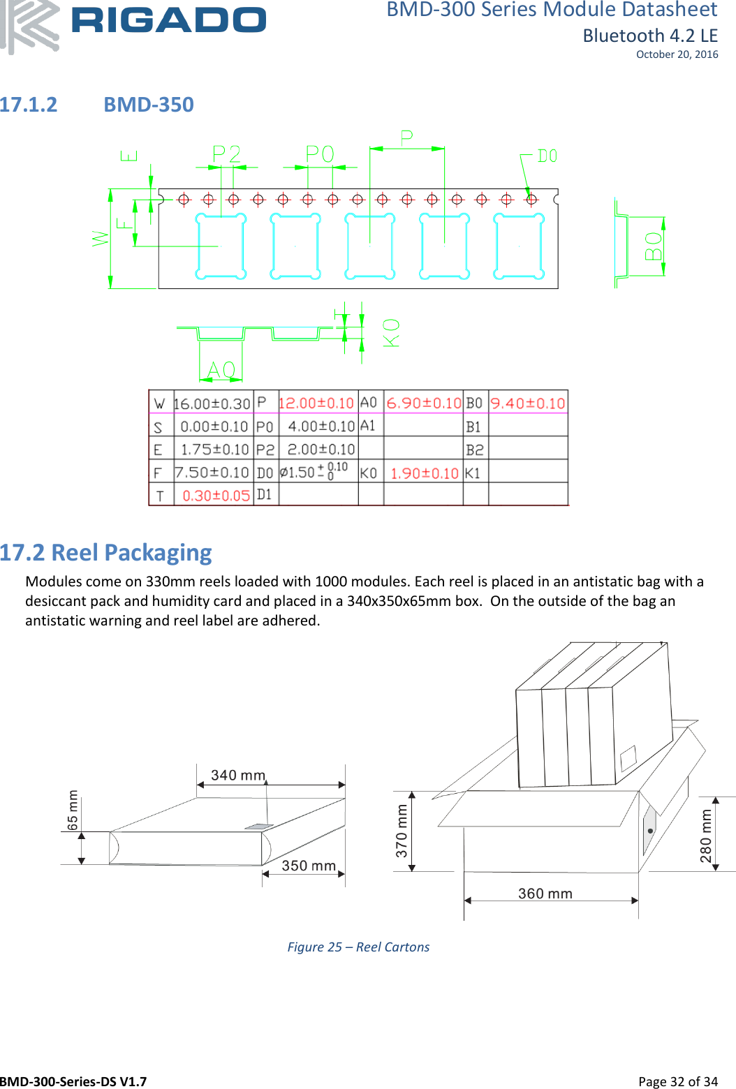
Rigado LLC BMD-350 BMD 300 Series Datasheet
UserManual.wiki
>
u blox
>
05 User Manual
Users manual
Navigation menu
Upload a User Manual
Namespaces
Wiki Guide
HTML
PDF
Info
Views
User Manual
Discussion / Help
Navigation
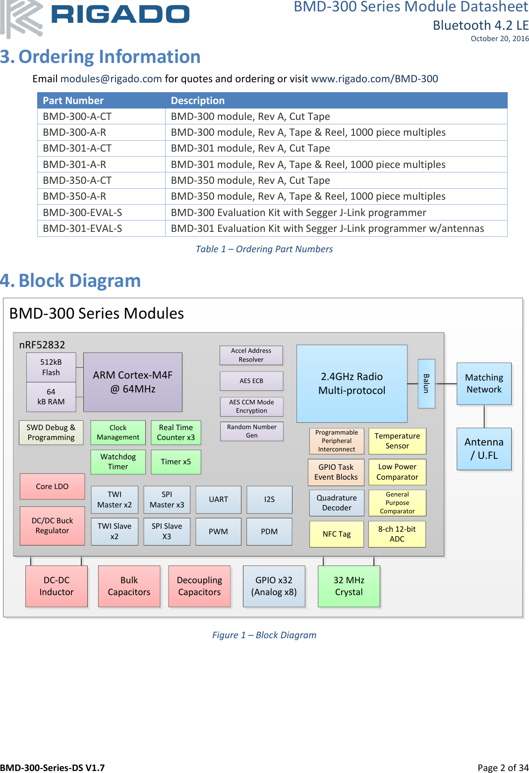
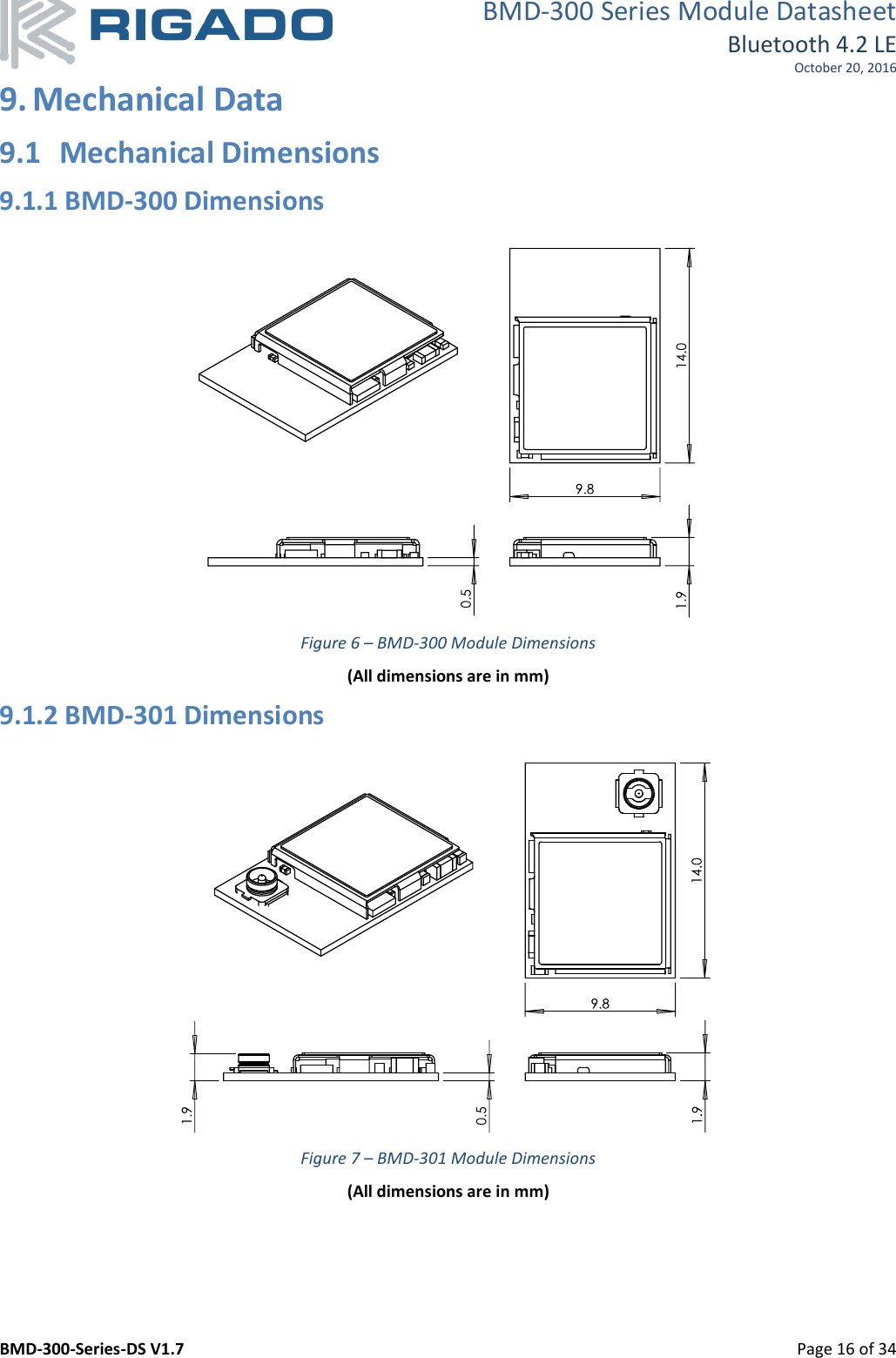
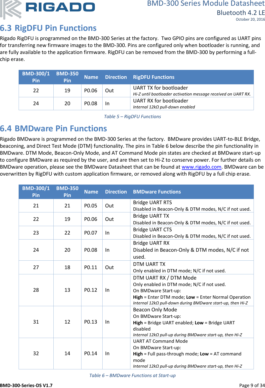
![BMD-300 Series Module Datasheet Bluetooth 4.2 LE October 20, 2016 BMD-300-Series-DS V1.7 Page 6 of 34 6. Pin Descriptions 6.1 BMD-300 / BMD-301 Figure 2 – BMD-300/301 Pin out (Top View) Pin description Pin Name Direction Description 6 P0.25 In/Out GPIO2 7 P0.26 In/Out GPIO2 8 P0.27 In/Out GPIO2 9 P0.28 In/Out GPIO/AIN42 10 P0.29 In/Out GPIO/AIN52 11 P0.30 In/Out GPIO/AIN62 12 P0.31 In/Out GPIO/AIN72 13 P0.00 In/Out GPIO/XTAL1 (32.768kHz) 14 P0.01 In/Out GPIO/XTAL2 (32.768kHz) 15 P0.02 In/Out GPIO/AIN0 19 P0.03 In/Out GPIO/AIN1 20 P0.04 In/Out GPIO/AIN2 21 P0.05 In/Out GPIO/AIN3 22 P0.06 In/Out GPIO 23 P0.07 In/Out GPIO 24 P0.08 In/Out GPIO 25 P0.09 In/Out GPIO/NFC1 26 P0.10 In/Out GPIO/NFC2 27 P0.11 In/Out GPIO 28 P0.12 In/Out GPIO 31 P0.13 In/Out GPIO 32 P0.14 In/Out GPIO/TRACEDATA[3] 33 P0.15 In/Out GPIO/TRACEDATA[2]](https://usermanual.wiki/u-blox/05/User-Guide-3177148-Page-6.png)
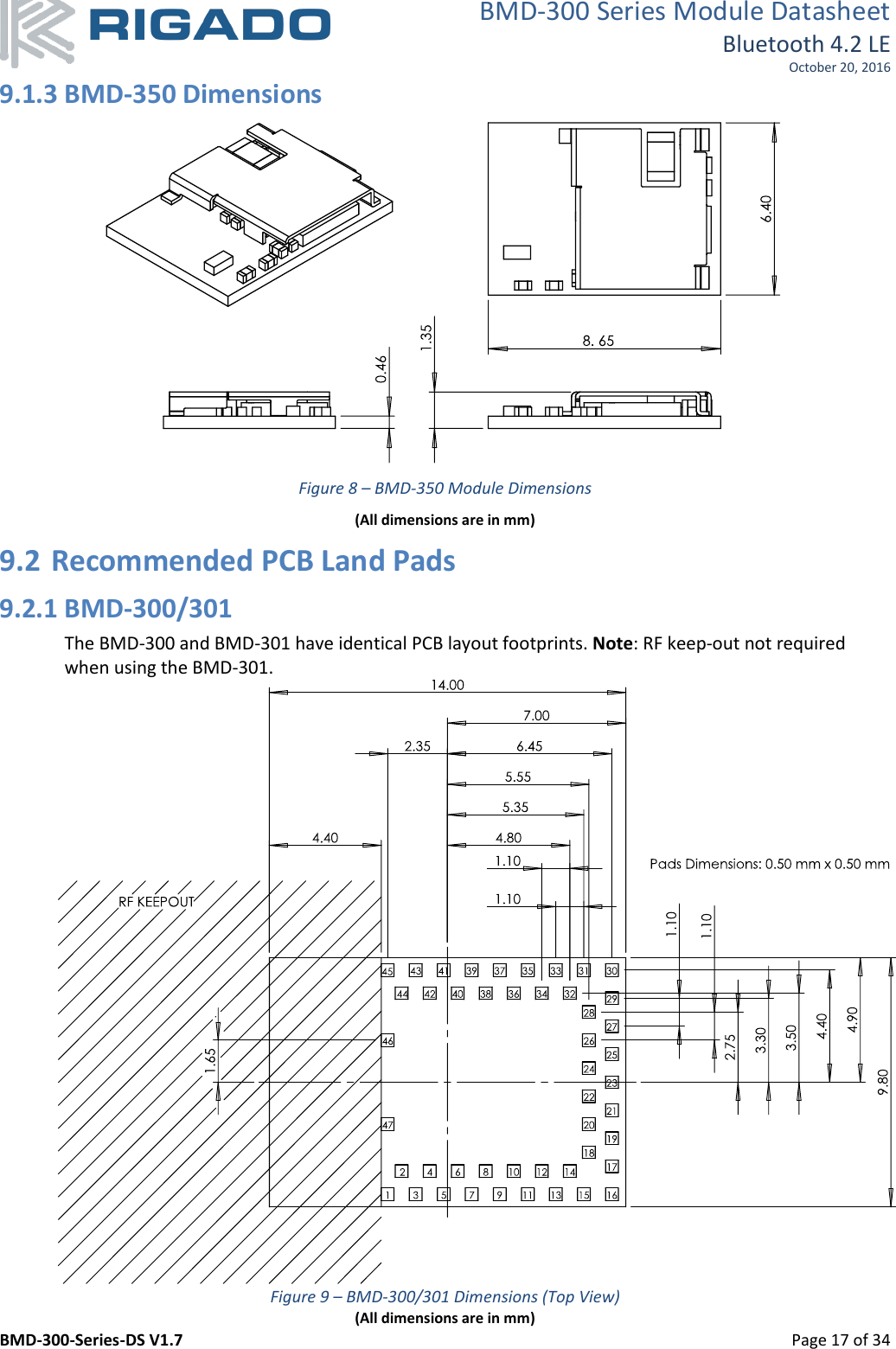
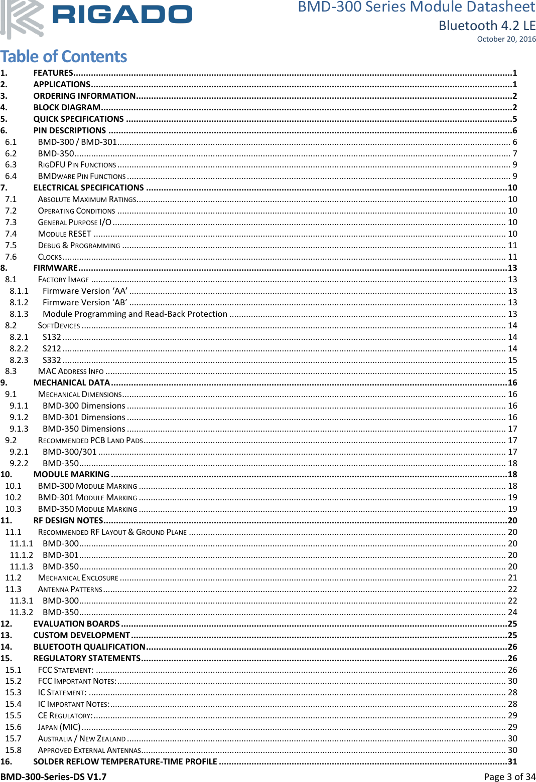
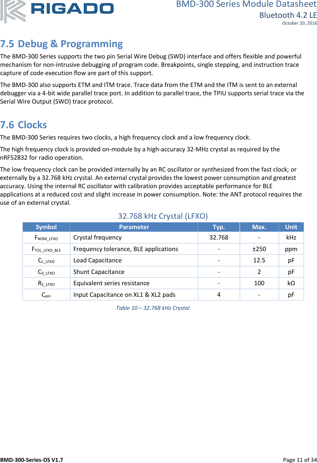
![BMD-300 Series Module Datasheet Bluetooth 4.2 LE October 20, 2016 BMD-300-Series-DS V1.7 Page 7 of 34 Pin Name Direction Description 34 P0.16 In/Out GPIO/TRACEDATA[1] 35 P0.17 In/Out GPIO 36 P0.18 In/Out GPIO/TRACEDATA[0]/SWO 37 P0.19 In/Out GPIO 38 P0.20 In/Out GPIO/TRACECLK 39 P0.21 In/Out GPIO/RESET̅̅̅̅̅̅̅̅ 40 P0.22 In/Out GPIO2 41 P0.23 In/Out GPIO2 42 P0.24 In/Out GPIO2 43 SWCLK In SWD Clock 44 SWDIO In/Out SWD IO 17 VCC Power +1.7V to +3.6V1 1, 2, 3, 4, 5, 16, 18, 29, 30, 45, 46, 47 GND Power Electrical Ground Note 1: An internal 4.7µF bulk capacitor is included on the module. However, it is good design practice to add additional bulk capacitance as required for your application, i.e. those with heavy GPIO usage and/or current draw. Note 2: These pins are in close proximity to the nRF52 radio power supply and antenna pins. Radio performance parameters, such as sensitivity, may be affected by high frequency digital I/O with large sink/source current on these pins. Nordic recommends using only low frequency, low-drive functions when possible. Table 3 – BMD-300/301 Pin Descriptions 6.2 BMD-350 Figure 3 – BMD-350 Pin out (Top View) Pin description Pin Name Direction Description 4 SWCLK In SWD Clock 5 SWDIO In/Out SWD IO 6 P0.20 In/Out GPIO/TRACECLK 7 P0.21 In/Out GPIO/RESET̅̅̅̅̅̅̅̅](https://usermanual.wiki/u-blox/05/User-Guide-3177148-Page-7.png)
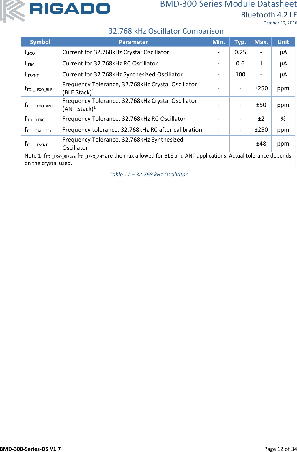
![BMD-300 Series Module Datasheet Bluetooth 4.2 LE October 20, 2016 BMD-300-Series-DS V1.7 Page 8 of 34 Pin Name Direction Description 8 P0.18 In/Out GPIO/TRACEDATA[0]/SWO 9 P0.16 In/Out GPIO/TRACEDATA[1] 10 P0.17 In/Out GPIO 11 P0.15 In/Out GPIO/TRACEDATA[2] 12 P0.13 In/Out GPIO 13 P0.12 In/Out GPIO 14 P0.14 In/Out GPIO/TRACEDATA[3] 16 P0.09 In/Out GPIO/NFC1 17 P0.10 In/Out GPIO/NFC2 18 P0.11 In/Out GPIO 19 P0.06 In/Out GPIO 20 P0.08 In/Out GPIO 21 P0.05 In/Out GPIO/AIN3 22 P0.07 In/Out GPIO 23 P0.01 In/Out GPIO/XTAL2 (32.768kHz) 24 P0.00 In/Out GPIO/XTAL1 (32.768kHz) 27 P0.04 In/Out GPIO/AIN2 28 P0.02 In/Out GPIO/AIN0 29 P0.30 In/Out GPIO/AIN62 30 P0.31 In/Out GPIO/AIN72 31 P0.29 In/Out GPIO/AIN52 32 P0.27 In/Out GPIO2 33 P0.25 In/Out GPIO2 34 P0.26 In/Out GPIO2 35 P0.23 In/Out GPIO2 36 P0.24 In/Out GPIO2 41 P0.22 In/Out GPIO2 42 P0.19 In/Out GPIO 44 P0.03 In/Out GPIO/AIN1 45 P0.28 In/Out GPIO/AIN42 25 VCC Power +1.7V to +3.6V1 1, 2, 3, 15, 26, 37, 38, 39, 40, 43, 46, 47 GND Power Electrical Ground Note 1: An internal 4.7µF bulk capacitor is included on the module. However, it is good design practice to add additional bulk capacitance as required for your application, i.e. those with heavy GPIO usage and/or current draw. Note 2: These pins are in close proximity to the nRF52 radio power supply and antenna pins. Radio performance parameters, such as sensitivity, may be affected by high frequency digital I/O with large sink/source current on these pins. Nordic recommends using only low frequency, low-drive functions when possible. Table 4 – BMD-350 Pin Descriptions](https://usermanual.wiki/u-blox/05/User-Guide-3177148-Page-8.png)
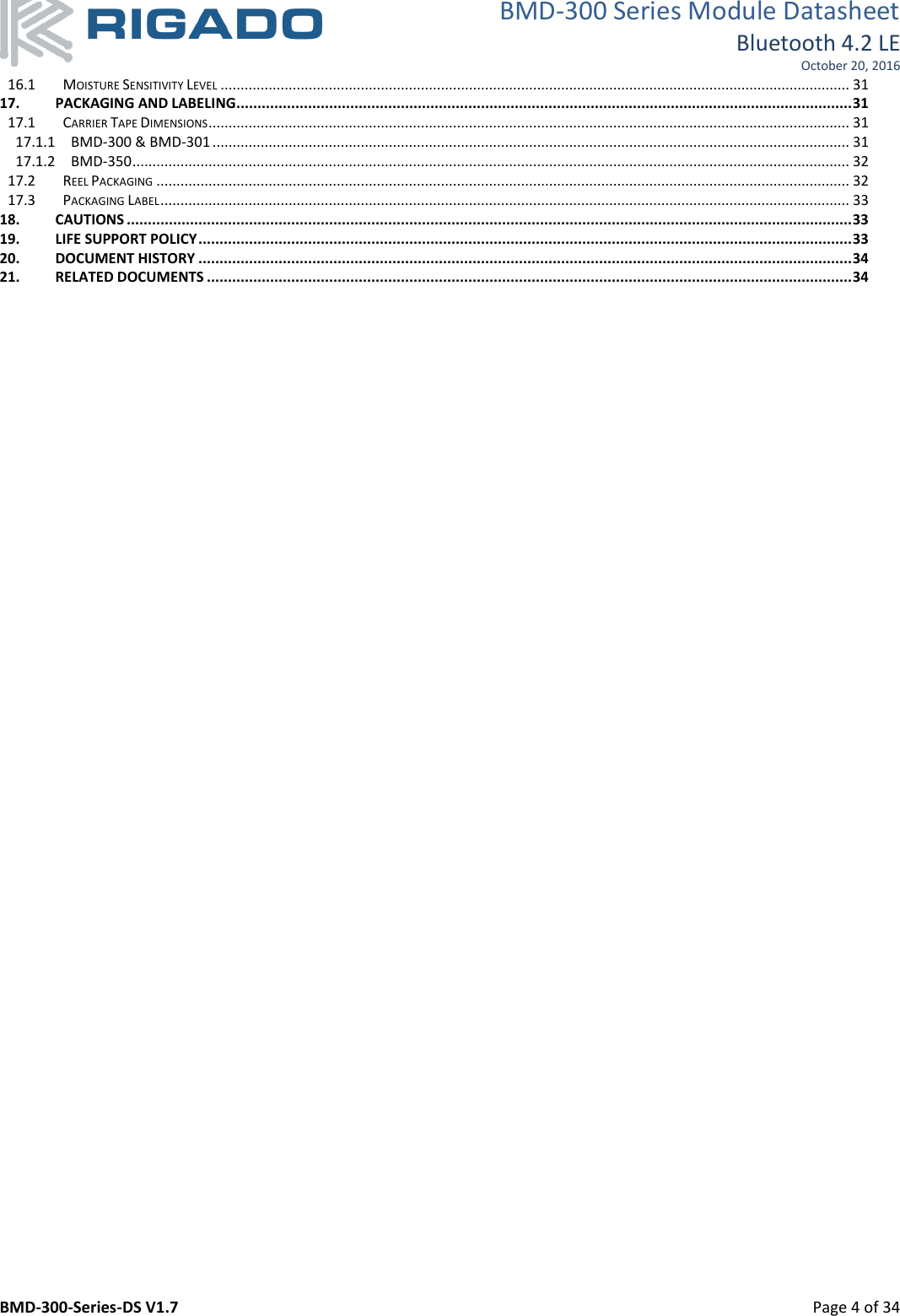
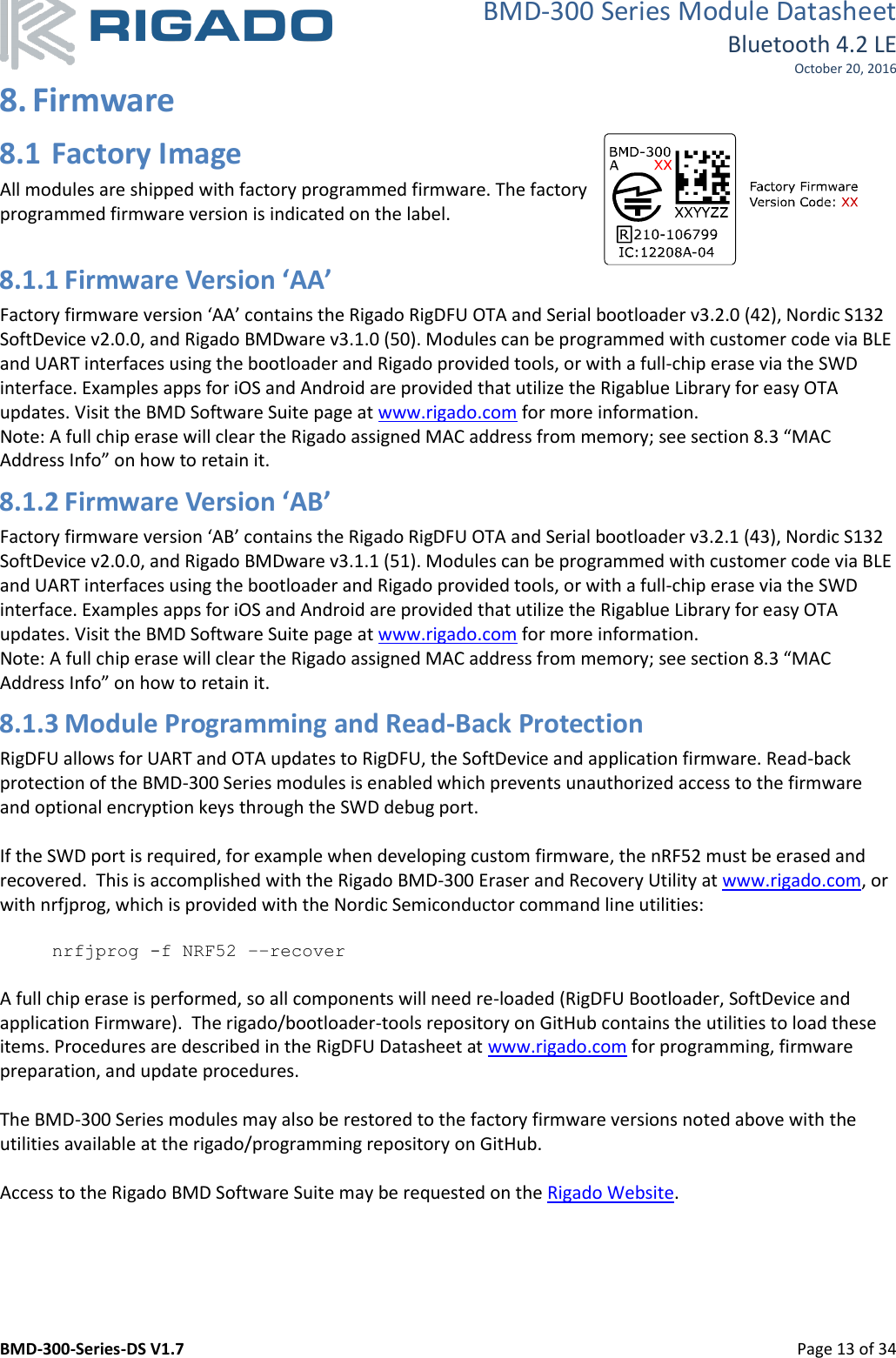
![BMD-300 Series Module Datasheet Bluetooth 4.2 LE October 20, 2016 BMD-300-Series-DS V1.7 Page 10 of 34 7. Electrical Specifications 7.1 Absolute Maximum Ratings Symbol Parameter Min. Max. Unit VCC_MAX Voltage on supply pin -0.3 3.9 V VIO_MAX Voltage on GPIO pins (VCC > 3.6V) -0.3 3.9 V VIO_MAX Voltage on GPIO pins (VCC ≤ 3.6V) -0.3 VCC + 0.3V V TS Storage Temperature Range -40 125 °C Table 7 – Absolute Maximum Ratings 7.2 Operating Conditions Symbol Parameter Min. Typ. Max. Unit VCC Operating supply voltage 1.7 3.0 3.6 V TR_VCC Supply rise time (0V to 1.7V) - - 60 ms TA Operating Ambient Temperature Range -40 25 85 °C Table 8 – Operating Conditions 7.3 General Purpose I/O The general purpose I/O is organized as one port enabling access and control of the 32 available GPIO pins through one port. Each GPIO can be accessed individually with the following user configurable features: Input/output direction Output drive strength Internal pull-up and pull-down resistors Wake-up from high or low level triggers on all pins Trigger interrupt on all pins All pins can be used by the PPI task/event system; the maximum number of pins that can be interfaced through the PPI at the same time is limited by the number of GPIOTE channels All pins can be individually configured to carry serial interface or quadrature demodulator signals Symbol Parameter Min. Typ. Max. Unit VIH Input High Voltage 0.7 x VCC - VCC V VIL Input Low Voltage VSS - 0.3 x VCC V VOH Output High Voltage VCC − 0.4 - VCC V VOL Output Low Voltage VSS - VSS + 0.4 V RPU Pull-up Resistance 11 13 16 kΩ RPD Pull-down Resistance 11 13 16 kΩ Table 9 – GPIO 7.4 Module RESET GPIO pin P0.21 may be used for a hardware reset. In order to utilize P0.21 as a hardware reset, the UICR registers PSELRESET[0] and PSELRESET[1] must be set alike, to the value of 0x7FFFFF15. When P0.21 is programmed as RESET̅̅̅̅̅̅̅̅, the internal pull-up is automatically enabled. Rigado and Nordic example applications and development kits program P0.21 as RESET̅̅̅̅̅̅̅̅.](https://usermanual.wiki/u-blox/05/User-Guide-3177148-Page-10.png)
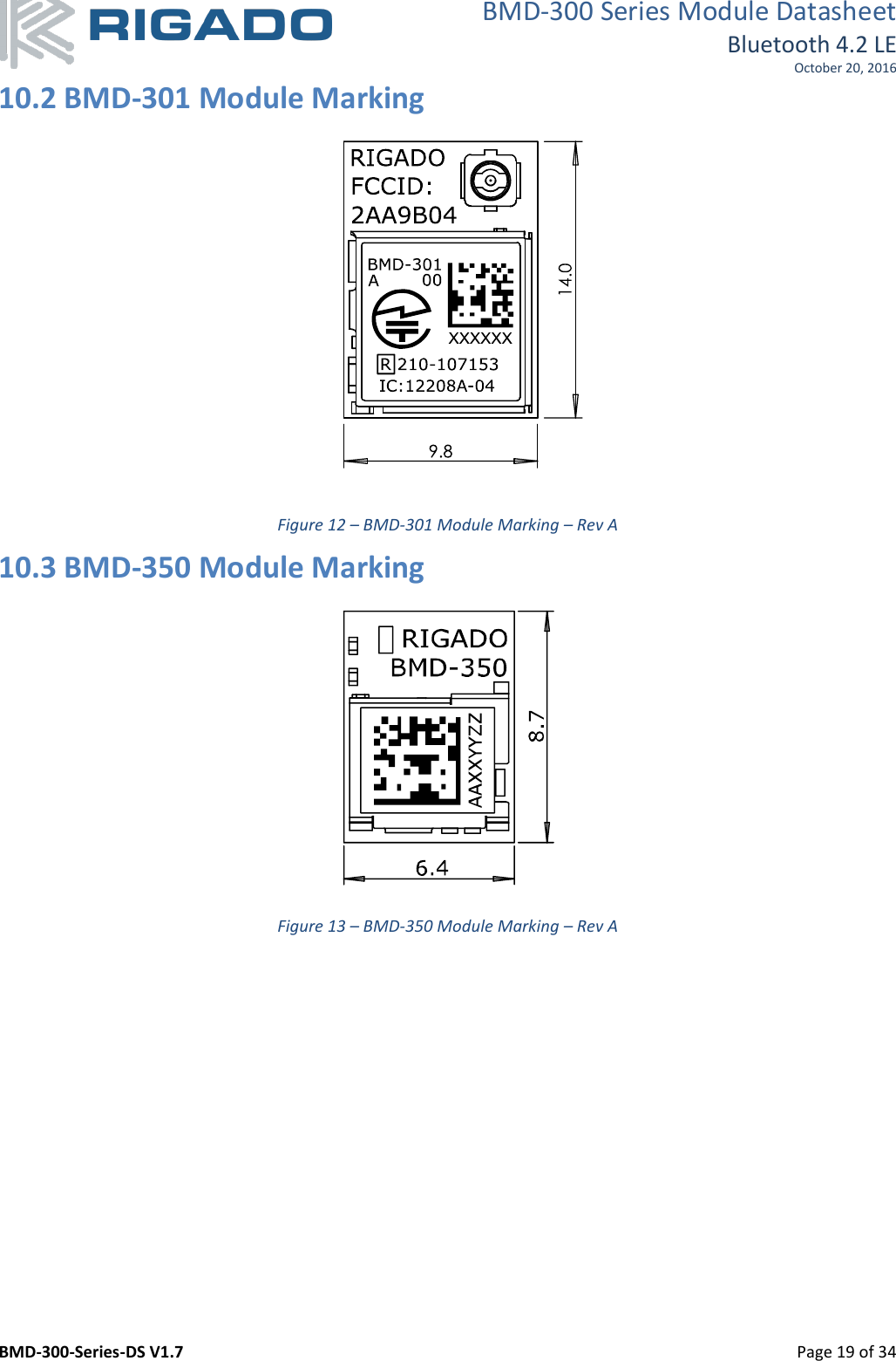
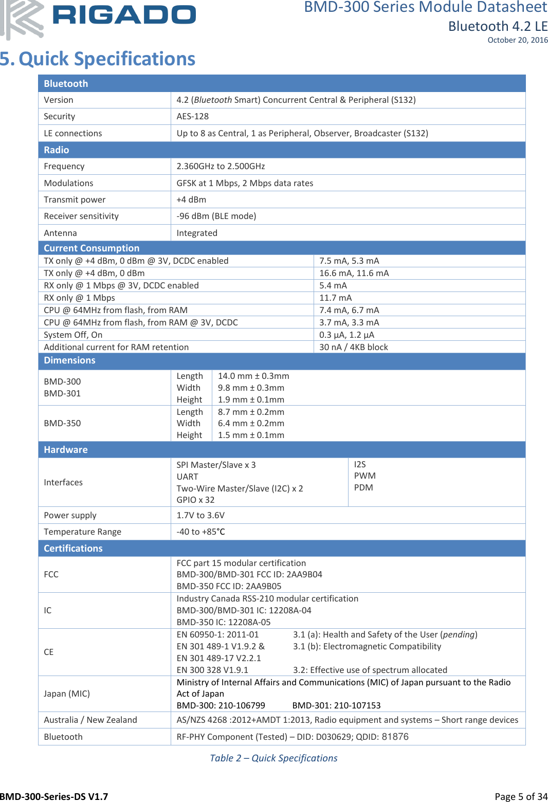
![BMD-300 Series Module Datasheet Bluetooth 4.2 LE October 20, 2016 BMD-300-Series-DS V1.7 Page 15 of 34 SoftDevice features Built-in NVM access and radio coexistence management Master Boot Record for over-the air device firmware update Memory isolation between application and protocol stack for robustness and security Thread-safe supervisor-call based API Asynchronous, event-driven behavior No RTOS dependency o Any RTOS can be used o No link-time dependencies o Standard ARM® Cortex™ -M4F project configuration for application development Support for concurrent and non-concurrent multiprotocol operation Concurrent multiprotocol timeslot API Alternate protocol stack running in application space 8.2.3 S332 The S332 SoftDevice is a combined ANT™ and Bluetooth® low energy (BLE) protocol stack solution. It supports all four Bluetooth low energy roles (central, peripheral, observer, broadcaster) and ANT. The S332 SoftDevice provides a full and flexible Application Programming Interface (API) for building concurrent ANT and BLE System on Chip (SoC) solutions. It simplifies combining an ANT and BLE protocol stack and an application on the same CPU, therefore eliminating the need for an added device to support concurrent multiprotocol. 8.3 MAC Address Info The BMD-300 Series modules comes preprogrammed with a unique MAC address from the factory. The MAC address is also printed on a 2D barcode on the top of the module. Figure 4 – BMD-300/301 MAC Address on Label Figure 5 – BMD-350 MAC Address on Label The 6-byte BLE Radio MAC address is stored in the nRF52832 UICR at NRF_UICR_BASE+0x80 LSB first. Please read the MAC Address Provisioning application note if you are not using the built in bootloader to avoid erasing/overwriting the MAC address during programming. Important: The BMD-300 comes with full memory protection enabled, not allowing the UICR to be read via the SWD interface. If performing a full-erase, the MAC can then only be recovered from the 2D barcode and human-readable text. UICR Register: NRF_UICR + 0x80 (0x10001080): MAC_Addr [0] (0xZZ) NRF_UICR + 0x81 (0x10001081): MAC_Addr [1] (0xYY) NRF_UICR + 0x82 (0x10001082): MAC_Addr [2] (0xXX) NRF_UICR + 0x83 (0x10001083): MAC_Addr [3] (0x93) NRF_UICR + 0x84 (0x10001084): MAC_Addr [4] (0x54) NRF_UICR + 0x85 (0x10001085): MAC_Addr [5] (0x94)](https://usermanual.wiki/u-blox/05/User-Guide-3177148-Page-15.png)