u blox 10 BMD-340 User Manual BMD 340 Datasheet
Rigado, Inc. BMD-340 BMD 340 Datasheet
UserManual.wiki
>
u blox
>
10 User Manual
User Manual
Navigation menu
Upload a User Manual
Namespaces
Wiki Guide
HTML
PDF
Info
Views
User Manual
Discussion / Help
Navigation
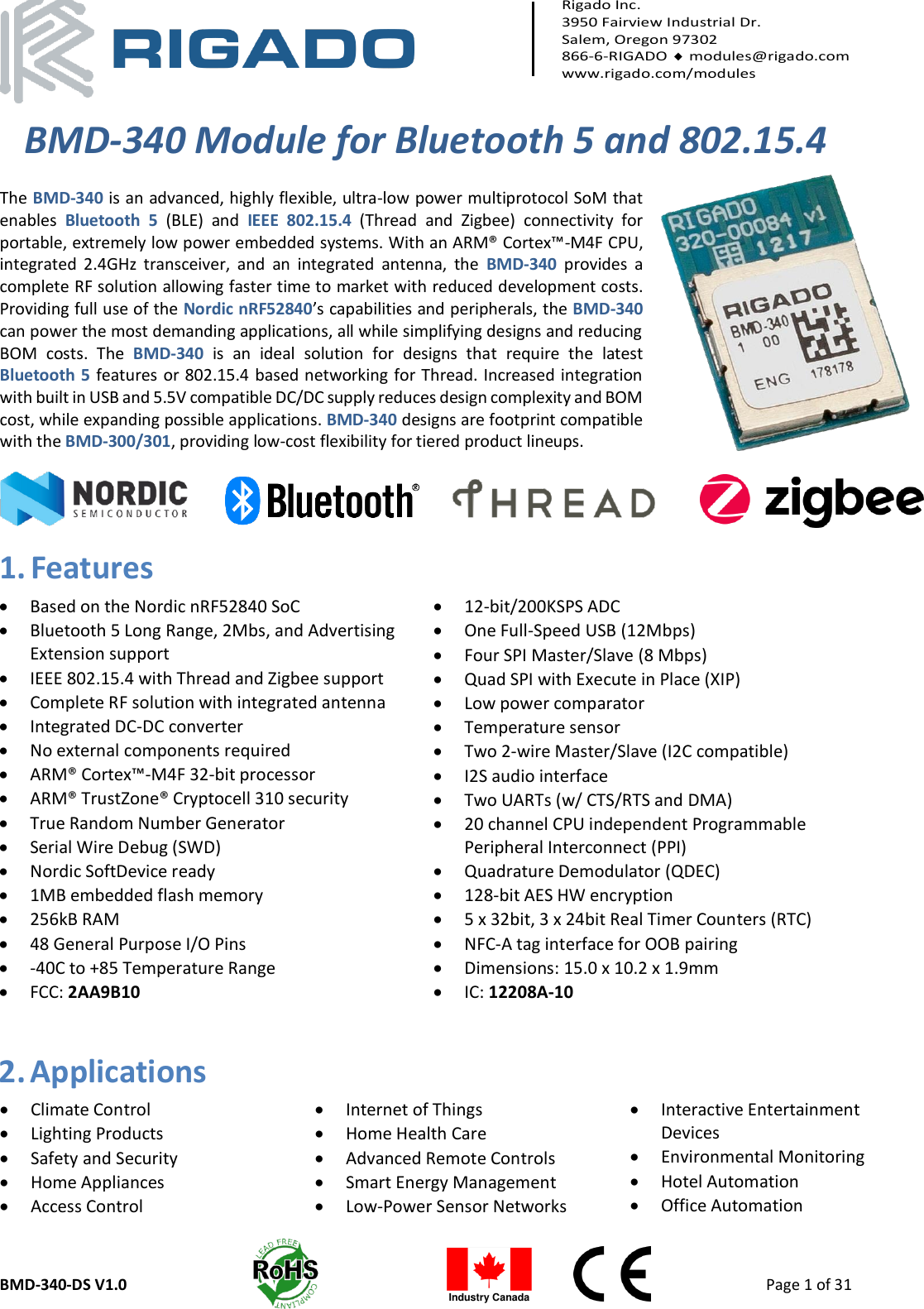
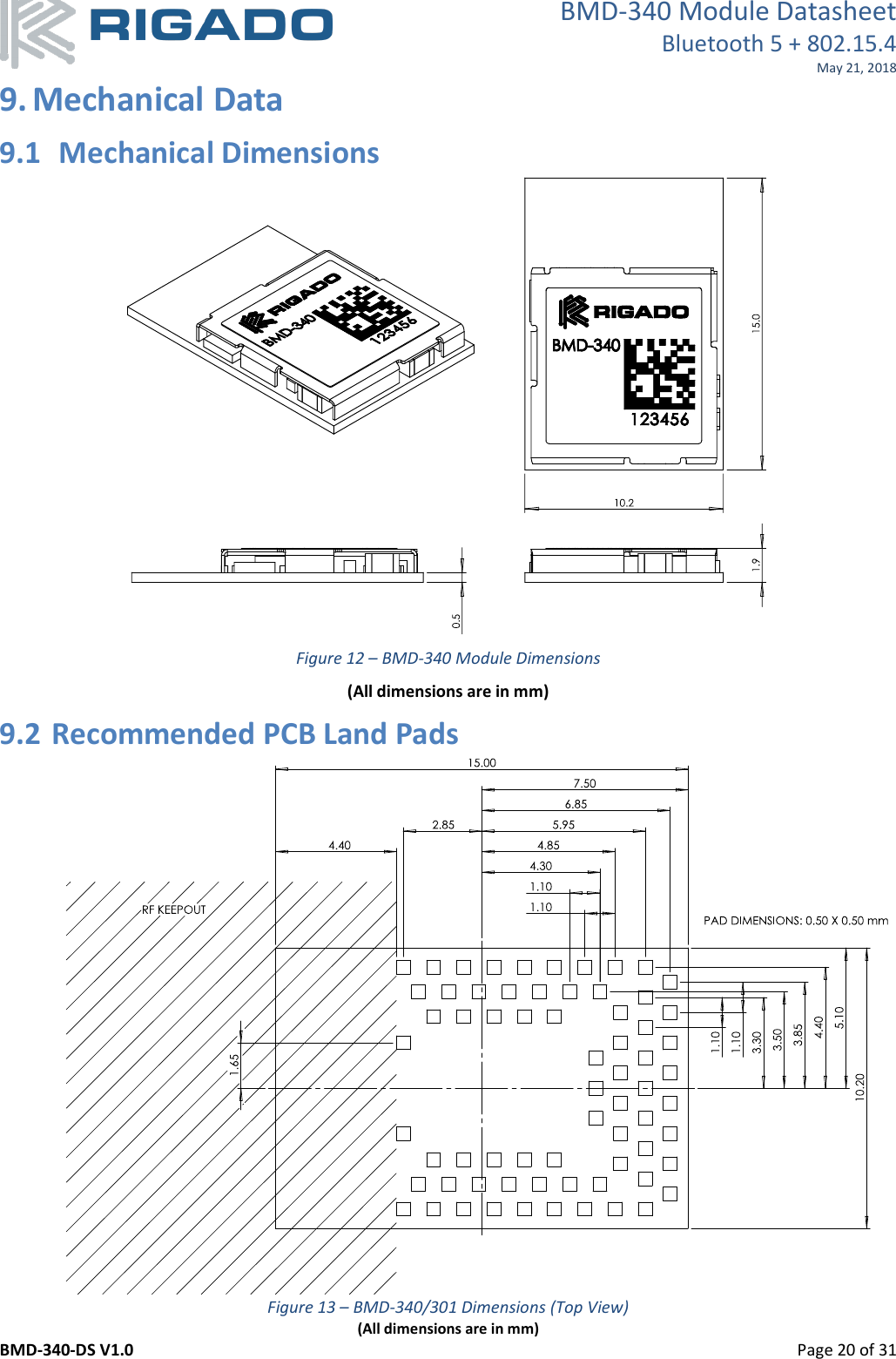
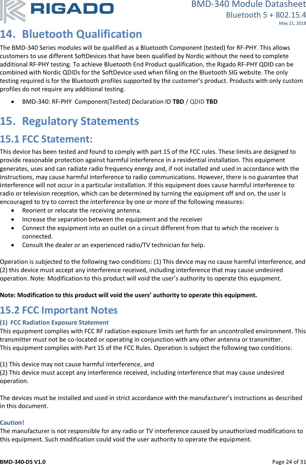
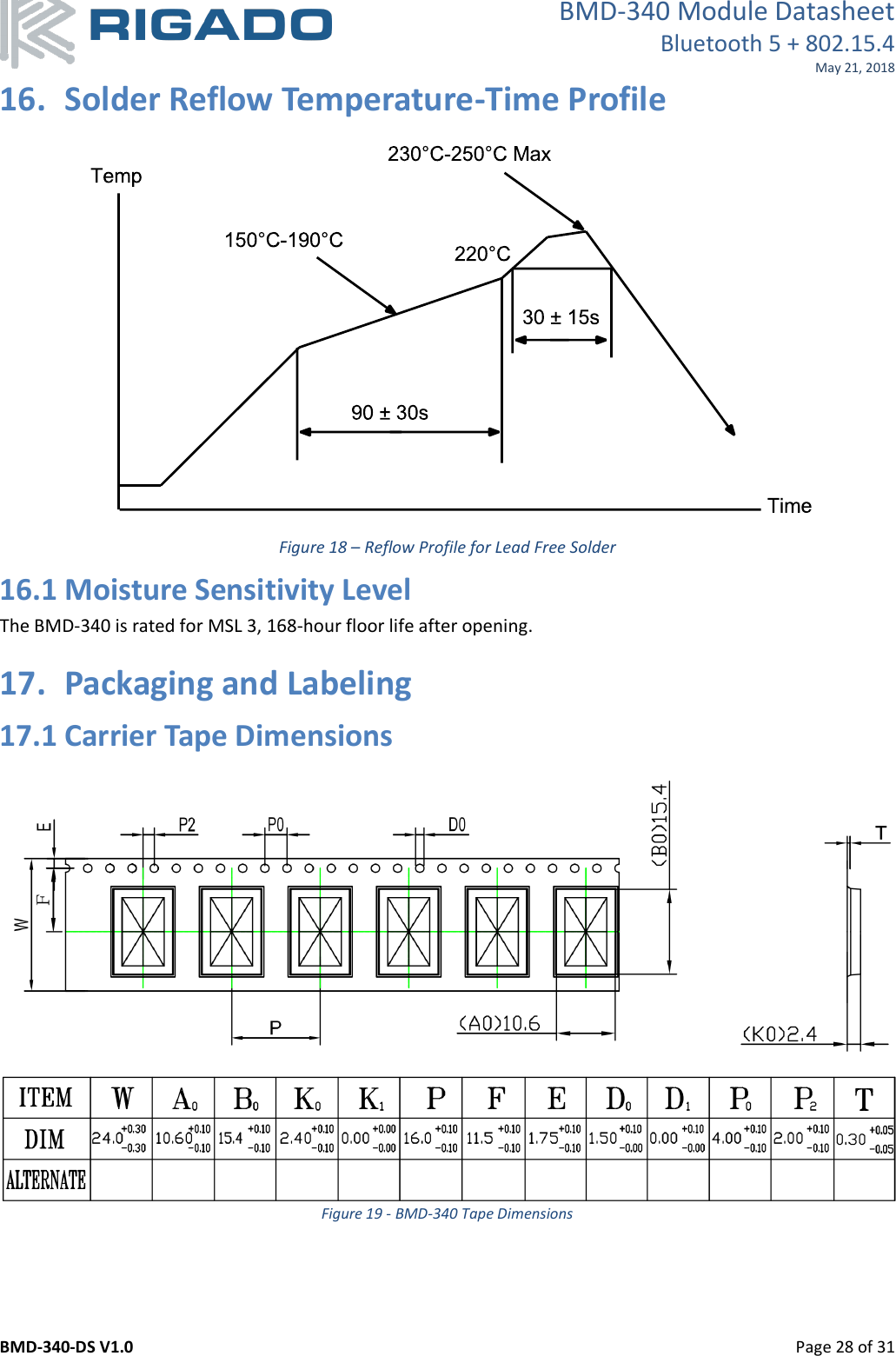
![BMD-340 Module Datasheet Bluetooth 5 + 802.15.4 May 21, 2018 BMD-340-DS V1.0 Page 6 of 31 6. Pin Descriptions 6.1 BMD-340 Figure 2 – BMD-340 Pin out (Top View) Pin description Pin Name Direction Description 6 P0.25 In/Out GPIO 7 P0.26 In/Out GPIO 8 P0.27 In/Out GPIO 9 P0.28 In/Out GPIO/AIN42 10 P0.29 In/Out GPIO/AIN52 11 P0.30 In/Out GPIO/AIN62 12 P0.31 In/Out GPIO/AIN72 13 P0.00 In/Out GPIO/XTAL1 (32.768kHz) 14 P0.01 In/Out GPIO/XTAL2 (32.768kHz) 15 P0.02 In/Out GPIO/AIN02 19 P0.03 In/Out GPIO/AIN12 20 P0.04 In/Out GPIO/AIN2 21 P0.05 In/Out GPIO/AIN3 22 P0.06 In/Out GPIO 23 P0.07 In/Out GPIO/TRACECLK 24 P0.08 In/Out GPIO 25 P0.09 In/Out GPIO/NFC12 26 P0.10 In/Out GPIO/NFC22 27 P0.11 In/Out GPIO/TRACEDATA[2] 28 P0.12 In/Out GPIO/TRACEDATA[1] 31 P0.13 In/Out GPIO 32 P0.14 In/Out GPIO](https://usermanual.wiki/u-blox/10/User-Guide-3900857-Page-6.png)
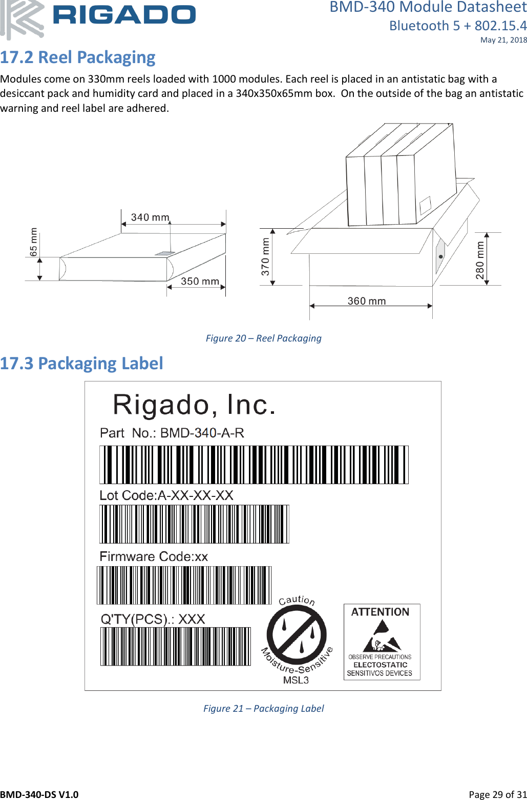
![BMD-340 Module Datasheet Bluetooth 5 + 802.15.4 May 21, 2018 BMD-340-DS V1.0 Page 7 of 31 Pin Name Direction Description 33 P0.15 In/Out GPIO 34 P0.16 In/Out GPIO 35 P0.17 In/Out GPIO 36 P0.21 In/Out GPIO 37 P0.19 In/Out GPIO 38 P0.20 In/Out GPIO 39 P0.18 In/Out GPIO/RESET̅̅̅̅̅̅̅̅ 40 P0.22 In/Out GPIO 41 P0.23 In/Out GPIO 42 P0.24 In/Out GPIO 43 SWCLK In SWD Clock 44 SWDIO In/Out SWD IO 48 P1.05 In/Out GPIO2 49 P1.06 In/Out GPIO2 50 P1.07 In/Out GPIO2 51 P1.08 In/Out GPIO 52 P1.09 In/Out GPIO/TRACEDATA[3] 53 P1.10 In/Out GPIO2 54 P1.11 In/Out GPIO2 56 P1.00 In/Out GPIO/TRACEDATA[0]/SWO 57 P1.01 In/Out GPIO2 58 P1.02 In/Out GPIO2 59 P1.03 In/Out GPIO2 60 P1.04 In/Out GPIO2 61 P1.12 In/Out GPIO2 62 P1.13 In/Out GPIO2 63 P1.14 In/Out GPIO2 64 P1.15 In/Out GPIO2 67 USB-D- In/Out USB Data - 68 USB-D+ In/Out USB Data + 66 VBUS Power USB PHY supply: 4.35V to 5.5V in Connect to USB Host device 5V supply 17 VCC1 Power In/Out LV Mode: 1.7V to 3.6V in HV Mode: 1.8V to 3.3V supply out3 65 VCCH1 Power LV Mode: Connect to VCC HV Mode: 2.5V to 5.5V in 1, 2, 3, 4, 5, 16, 18, 29, 30, 45, 46, 47, 55 GND Power Electrical Ground Note 1: An internal 4.7µF bulk capacitor is included on the module. However, it is good design practice to add additional bulk capacitance as required for your application, i.e. those with heavy GPIO usage and/or current draw. Note 2: These pins are in close proximity to the nRF52 radio power supply and antenna pins. Radio performance parameters, such as sensitivity, may be affected by high frequency digital I/O with large sink/source current on these pins. Nordic recommends using only low frequency, low-drive functions when possible. Note 3: In HV mode, VCC acts as a regulated supply that can power other external devices. The voltage output of VCC can be configured in software but is limited to no more than VCCH-0.3V. In System Off mode VCC can supply no more than 1mA. Table 3 – BMD-340 Pin Descriptions](https://usermanual.wiki/u-blox/10/User-Guide-3900857-Page-7.png)
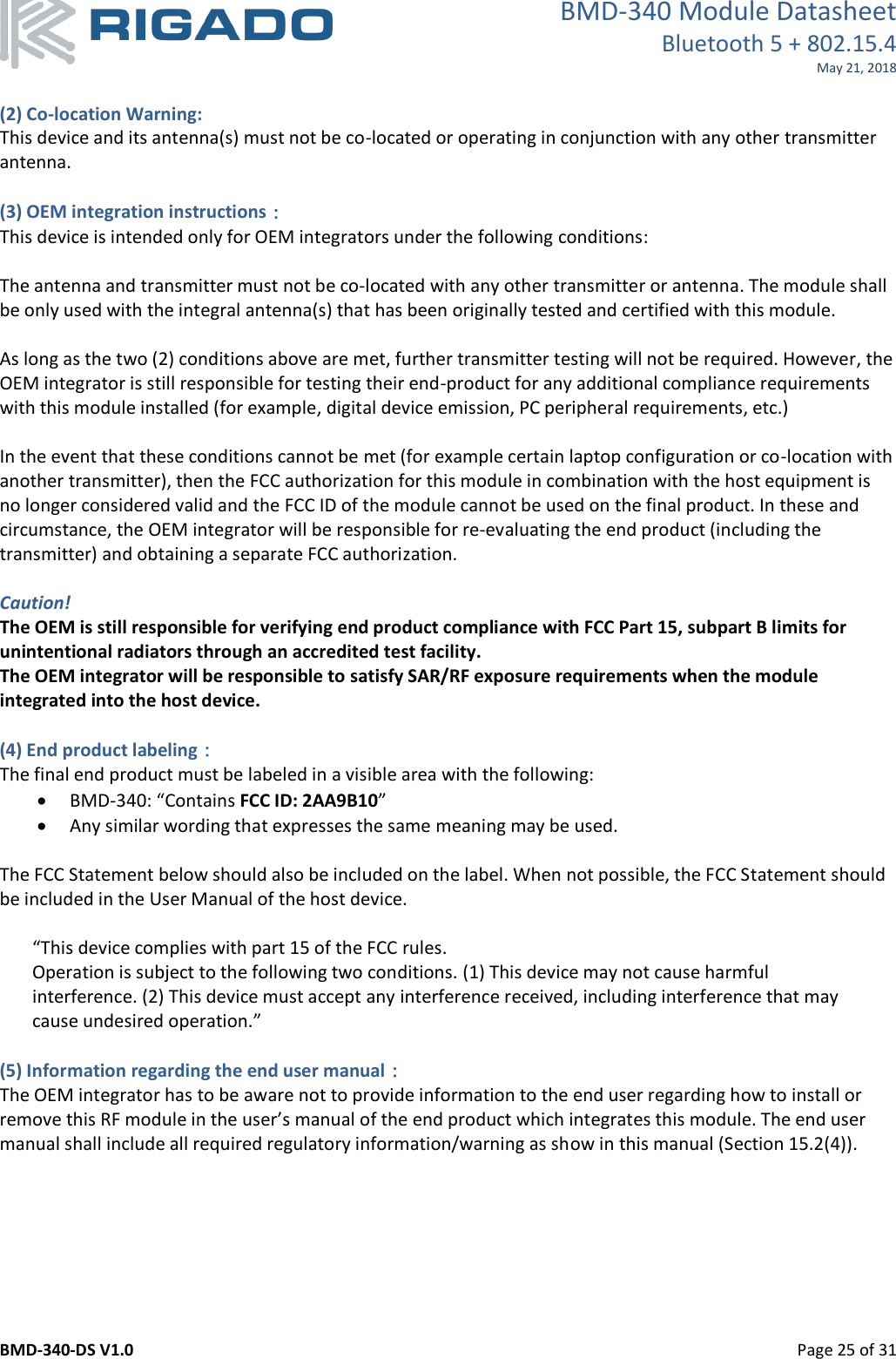
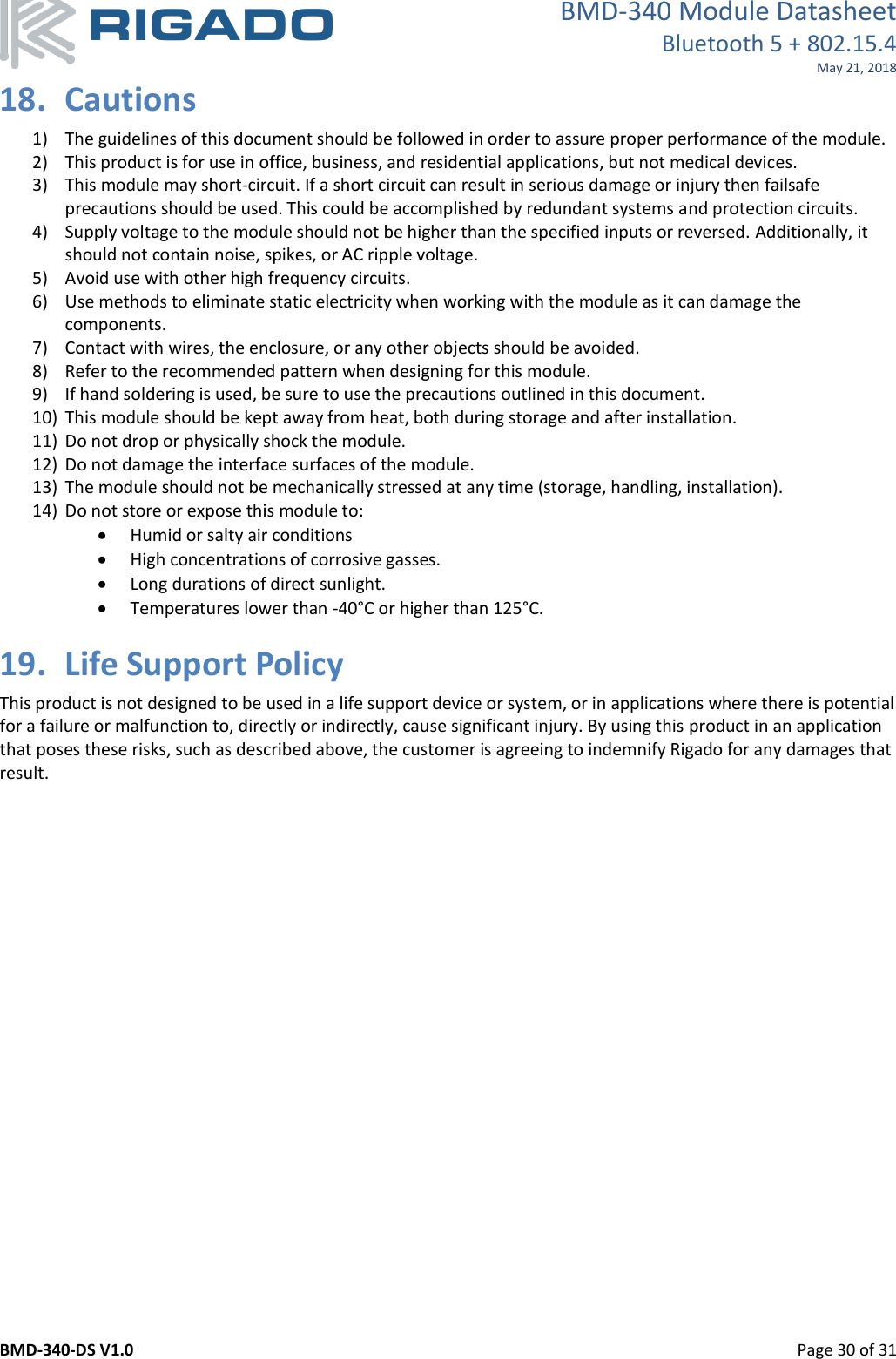
![BMD-340 Module Datasheet Bluetooth 5 + 802.15.4 May 21, 2018 BMD-340-DS V1.0 Page 8 of 31 6.2 Peripheral Pins The BMD-340 features a pin muxing system that allows most internal peripherals, such as UART and SPI, to be used on any GPIO pin. This freedom in pin choice enables better optimization of designs and PCB layout. Note that only one peripheral signal can be muxed to a GPIO pin at a time. Some functions are restricted to certain pins due to additional internal circuitry required by the interface. These include: Trace signals, analog inputs, XTAL signals, USB signals, SWD interface, and reset. See Table 4 below for details: Peripheral Signal Pin Options UART0, UART1 All P0.00-P0.31, P1.00-P1.15 I2C0, I2C1 SPI0, SPI1, SPI2, SPI3 I2S0 QSPI0 PWM0, PWM1, PWM2, PWM3 PDN0 ADC, COMP, LPCOMP All P0.02-P0.05, P0.28-P0.31 (AIN0-AIN7) NFC NFC1 P0.09 NFC2 P0.10 Reset RESET̅̅̅̅̅̅̅̅ P0.18 Trace TRACECLK P0.07 SWO/TRACEDATA[0] P1.00 TRACEDATA[1] P0.12 TRACEDATA[2] P0.11 TRACEDATA[3] P1.09 SWD SWD Clock SWCLK SWD IO SWDIO 32.768kHz Crystal XTAL1 P0.00 XTAL2 P0.01 USB USB Data + USB-D+ USB Data - USB-D- Table 4 – Peripheral Pin Options Note: Some peripherals on the BMD-340 share the same memory location for their registers. This means that only one of these peripherals can be used at a time. It is possible to switch between peripherals that share the same register location by clearing and reinitializing the associated configuration registers. See the Nordic Semiconductor nRF52840 Product Specification for details. Peripheral ID Base Address Shared Peripherals 3 0x40003000 SPI0 I2C0 4 0x40004000 SPI1 I2C1 Table 5 – Peripherals with Shared Registers](https://usermanual.wiki/u-blox/10/User-Guide-3900857-Page-8.png)
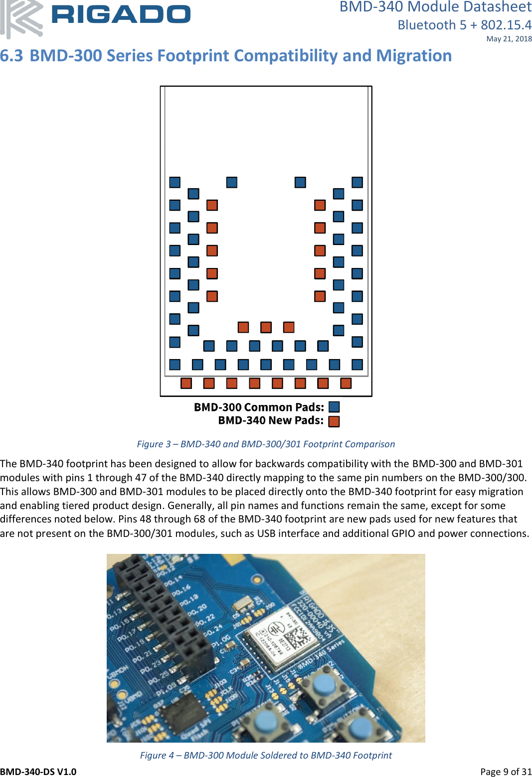
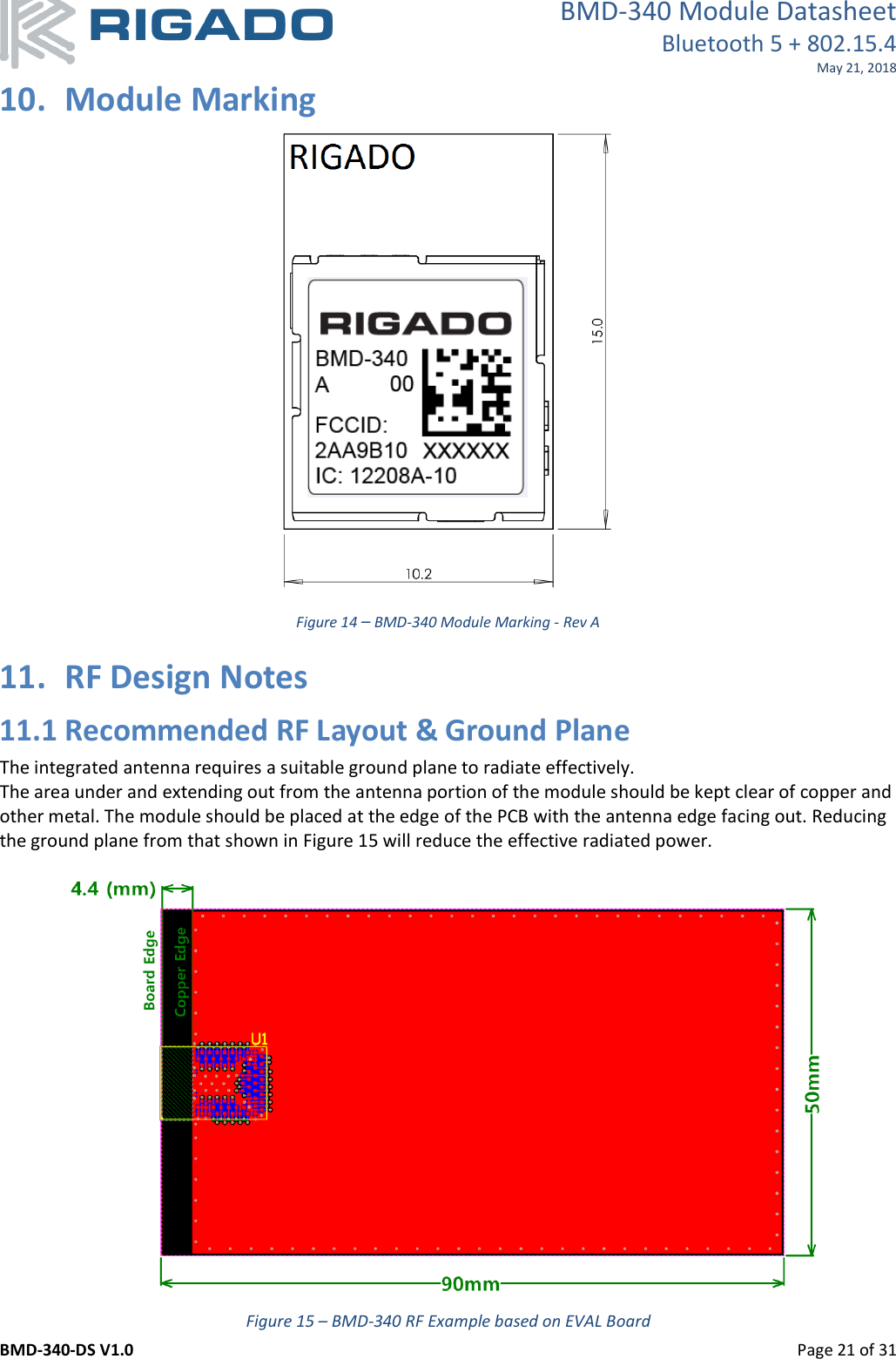
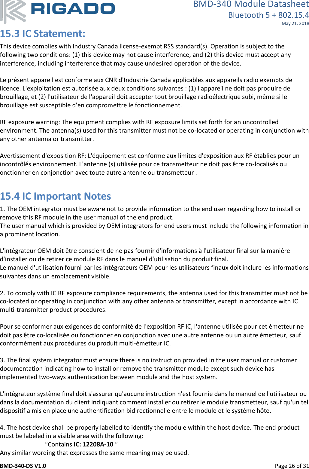
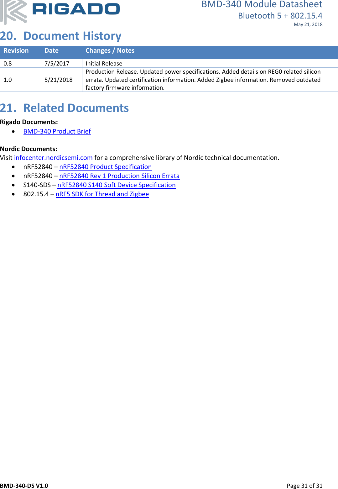
![BMD-340 Module Datasheet Bluetooth 5 + 802.15.4 May 21, 2018 BMD-340-DS V1.0 Page 10 of 31 6.3.1 BMD-300/301 to BMD-340 Pad Differences Due to changes in the nRF52840 SoC used by the BMD-340, not all functions (such as SWO/TRACE signals) are found on the same pins as on the BMD-300/301. Particularly of note is the reset pin function which on the BMD-340 is now available on P0.18 instead of P0.21 as on the BMD-300/301. To maintain pin for pin compatibility of the reset signal, P0.18 and P0.21 have swapped pad locations on the BMD-340 footprint. These differences are detailed in Table 6 below: Pin BMD-300/301 Name BMD-300/301 Function BMD-340 Name BMD-340 Function 39 P0.21 GPIO/RESET̅̅̅̅̅̅̅̅ P0.18 GPIO/RESET̅̅̅̅̅̅̅̅ 38 P0.20 GPIO/TRACECLK P0.20 GPIO 36 P0.18 GPIO/TRACEDATA[0]/SWO P0.21 GPIO 34 P0.16 GPIO/TRACEDATA[1] P0.16 GPIO 33 P0.15 GPIO/TRACEDATA[2] P0.15 GPIO 32 P0.14 GPIO/TRACEDATA[3] P0.14 GPIO 23 P0.07 GPIO P0.07 GPIO/TRACECLK 56 N/A N/A P1.00 GPIO/TRACEDATA[0]/SWO 28 P0.12 GPIO P0.12 GPIO/TRACEDATA[1] 27 P0.11 GPIO P0.11 GPIO/TRACEDATA[2] 52 N/A N/A P1.09 GPIO/TRACEDATA[3] Table 6 – BMD-300/301 to BMD-340 Pad Differences 6.3.2 BMD-300/301 to BMD-340 Design Migration Existing designs incorporating the BMD-300 or BMD-301 module can be migrated over to the BMD-340 with the addition of a single footprint pad for VCCH (pin 65). This migration option is only suitable for applications that do not require the new USB interface, additional GPIO, or higher supply voltage functionality. The VCCH pad must be present and electrically connected to the same supply as VCC in order for the module to operate correctly. Vias underneath the BMD-340 should be tented to avoid shorts to unused module pads. Firmware written for the BMD-300/301 can generally be ported to the BMD-340 with minimal effort. See the Nordic Semiconductor SDK documentation for details. Figure 5 – BMD-300 to BMD-340 Migration Example New Pad VCCH: Connect to VCC](https://usermanual.wiki/u-blox/10/User-Guide-3900857-Page-10.png)
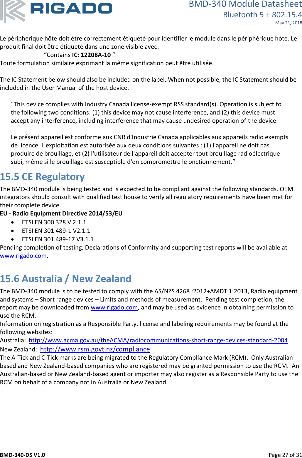
![BMD-340 Module Datasheet Bluetooth 5 + 802.15.4 May 21, 2018 BMD-340-DS V1.0 Page 12 of 31 7. Electrical Specifications 7.1 Absolute Maximum Ratings Symbol Parameter Min. Max. Unit VCC_MAX Voltage on VCC supply pin -0.3 3.9 V VCCH_MAX Voltage on VCCH supply pin -0.3 5.8 V VBUS_MAX Voltage on VBUS Supply pin -0.3 5.8 V VIO_MAX Voltage on GPIO pins (VCC > 3.6V) -0.3 3.9 V VIO_MAX Voltage on GPIO pins (VCC ≤ 3.6V) -0.3 VCC + 0.3V V TS Storage Temperature Range -40 125 °C Table 7 – Absolute Maximum Ratings 7.2 Operating Conditions Symbol Parameter Min. Typ. Max. Unit VCC_IN VCC operating supply voltage in 1.7 3.0 3.6 V VCC_START VCC DCDC starting voltage 1.75 - - V VCCH_HV VCCH operating supply voltage in 2.5 5.0 5.5 V VBUS_IN VBUS operating supply voltage in 4.35 5.0 5.5 V TR_VCC VCC Supply rise time (0V to 1.7V) - - 60 ms TR_VCCH VCCH Supply rise time (0V to 3.7V)1 - - 1 ms TA Operating Ambient Temperature Range -40 25 85 °C Note 1: Applies when module is configured to use HV mode. When using LV mode TR_VCC applies. See Nordic nRF52840 Rev 1 errata [202] for details on TR_VCCH requirement. Table 8 – Operating Conditions](https://usermanual.wiki/u-blox/10/User-Guide-3900857-Page-12.png)
![BMD-340 Module Datasheet Bluetooth 5 + 802.15.4 May 21, 2018 BMD-340-DS V1.0 Page 16 of 31 7.4 General Purpose I/O The general purpose I/O is organized as two ports enabling access and control of the 48 available GPIO pins. The first port allows access of P0.00 to P0.31, similar to the one port available on the BMD-300/301. The second port, new to the BMD-340, allows access to P1.00 to P1.15. Each GPIO can be accessed individually with the following user configurable features: • Input/output direction • Output drive strength • Internal pull-up and pull-down resistors • Wake-up from high or low level triggers on all pins • Trigger interrupt on all pins • All pins can be used by the PPI task/event system; the maximum number of pins that can be interfaced through the PPI at the same time is limited by the number of GPIOTE channels • All pins can be individually configured to carry serial interface or quadrature demodulator signals Symbol Parameter Min. Typ. Max. Unit VIH Input High Voltage 0.7 x VCC - VCC V VIL Input Low Voltage VSS - 0.3 x VCC V VOH Output High Voltage VCC − 0.4 - VCC V VOL Output Low Voltage VSS - VSS + 0.4 V RPU Pull-up Resistance 11 13 16 kΩ RPD Pull-down Resistance 11 13 16 kΩ Table 10 – GPIO 7.5 Module RESET GPIO pin P0.18 may be used for a hardware reset. In order to utilize P0.18 as a hardware reset, the UICR registers PSELRESET[0] and PSELRESET[1] must be set alike, to the value of 0x7FFFFFD2. When P0.18 is programmed as RESET̅̅̅̅̅̅̅̅, the internal pull-up is automatically enabled. Rigado and Nordic example applications and development kits program P0.18 as RESET̅̅̅̅̅̅̅̅. 7.6 Debug & Programming The BMD-340 supports the two pin Serial Wire Debug (SWD) interface and offers flexible and powerful mechanisms for non-intrusive debugging of program code. Breakpoints, single stepping, and instruction trace capture of code execution flow are part of this support. The BMD-340 also supports ETM and ITM trace. Trace data from the ETM and the ITM is sent to an external debugger via a 4-bit wide parallel trace port. In addition to parallel trace, the TPIU supports serial trace via the Serial Wire Output (SWO) trace protocol.](https://usermanual.wiki/u-blox/10/User-Guide-3900857-Page-16.png)
![BMD-340 Module Datasheet Bluetooth 5 + 802.15.4 May 21, 2018 BMD-340-DS V1.0 Page 19 of 31 8.4 MAC Address Info The BMD-340 modules comes preprogrammed with a unique MAC address from the factory. The MAC address is also printed on a 2D barcode on the top of the module. Figure 11 – BMD-340 MAC Address on Label The 6-byte BLE Radio MAC address is stored in the nRF52840 UICR at NRF_UICR_BASE+0x80 LSB first. Please read the MAC Address Provisioning application note if you are not using the built in bootloader to avoid erasing/overwriting the MAC address during programming. Important: If full memory protection is enabled, the UICR cannot be read via the SWD interface. If performing a full-erase, the MAC can then only be recovered from the 2D barcode and human-readable text. UICR Register: NRF_UICR + 0x80 (0x10001080): MAC_Addr [0] (0xZZ) NRF_UICR + 0x81 (0x10001081): MAC_Addr [1] (0xYY) NRF_UICR + 0x82 (0x10001082): MAC_Addr [2] (0xXX) NRF_UICR + 0x83 (0x10001083): MAC_Addr [3] (0x93) NRF_UICR + 0x84 (0x10001084): MAC_Addr [4] (0x54) NRF_UICR + 0x85 (0x10001085): MAC_Addr [5] (0x94)](https://usermanual.wiki/u-blox/10/User-Guide-3900857-Page-19.png)