User Manual

BMD-340-DS V1.0 Page 1 of 31
Rigado Inc.
3950 Fairview Industrial Dr.
Salem, Oregon 97302
866-6-RIGADO
modules@rigado.com
www.rigado.com/modules
BMD-340 Module for Bluetooth 5 and 802.15.4
The BMD-340 is an advanced, highly flexible, ultra-low power multiprotocol SoM that
enables Bluetooth 5 (BLE) and IEEE 802.15.4 (Thread and Zigbee) connectivity for
portable, extremely low power embedded systems. With an ARM® Cortex™-M4F CPU,
integrated 2.4GHz transceiver, and an integrated antenna, the BMD-340 provides a
complete RF solution allowing faster time to market with reduced development costs.
Providing full use of the Nordic nRF52840’s capabilities and peripherals, the BMD-340
can power the most demanding applications, all while simplifying designs and reducing
BOM costs. The BMD-340 is an ideal solution for designs that require the latest
Bluetooth 5 features or 802.15.4 based networking for Thread. Increased integration
with built in USB and 5.5V compatible DC/DC supply reduces design complexity and BOM
cost, while expanding possible applications. BMD-340 designs are footprint compatible
with the BMD-300/301, providing low-cost flexibility for tiered product lineups.
1. Features
• Based on the Nordic nRF52840 SoC
• Bluetooth 5 Long Range, 2Mbs, and Advertising
Extension support
• IEEE 802.15.4 with Thread and Zigbee support
• Complete RF solution with integrated antenna
• Integrated DC-DC converter
• No external components required
• ARM® Cortex™-M4F 32-bit processor
• ARM® TrustZone® Cryptocell 310 security
• True Random Number Generator
• Serial Wire Debug (SWD)
• Nordic SoftDevice ready
• 1MB embedded flash memory
• 256kB RAM
• 48 General Purpose I/O Pins
• -40C to +85 Temperature Range
• FCC: 2AA9B10
• 12-bit/200KSPS ADC
• One Full-Speed USB (12Mbps)
• Four SPI Master/Slave (8 Mbps)
• Quad SPI with Execute in Place (XIP)
• Low power comparator
• Temperature sensor
• Two 2-wire Master/Slave (I2C compatible)
• I2S audio interface
• Two UARTs (w/ CTS/RTS and DMA)
• 20 channel CPU independent Programmable
Peripheral Interconnect (PPI)
• Quadrature Demodulator (QDEC)
• 128-bit AES HW encryption
• 5 x 32bit, 3 x 24bit Real Timer Counters (RTC)
• NFC-A tag interface for OOB pairing
• Dimensions: 15.0 x 10.2 x 1.9mm
• IC: 12208A-10
2. Applications
• Climate Control
• Lighting Products
• Safety and Security
• Home Appliances
• Access Control
• Internet of Things
• Home Health Care
• Advanced Remote Controls
• Smart Energy Management
• Low-Power Sensor Networks
• Interactive Entertainment
Devices
• Environmental Monitoring
• Hotel Automation
• Office Automation
Industry Canada
BMD-340 Module Datasheet
Bluetooth 5 + 802.15.4
May 16, 2018
BMD-340-DS V1.0 Page 2 of 31
3. Ordering Information
Email modules@rigado.com for quotes and ordering or visit www.rigado.com/BMD-340
Part Number
Description
BMD-340-A-R
BMD-340 module, Rev A, nRF52840-QIAA, Tape & Reel, 1000 piece multiples
BMD-340-ES1
BMD-340 module, ENG, nRF52840-QIAA, Engineering A silicon
BMD-340-ES2
BMD-340 module, ENG, nRF52840-QIAA, Engineering B silicon
BMD-340-A-EVK
BMD-340-A Evaluation Kit with Segger J-Link programmer
BMD-340-ES1-EVK
BMD-340-ES1 Evaluation Kit with Segger J-Link programmer
Table 1 – Ordering Part Numbers
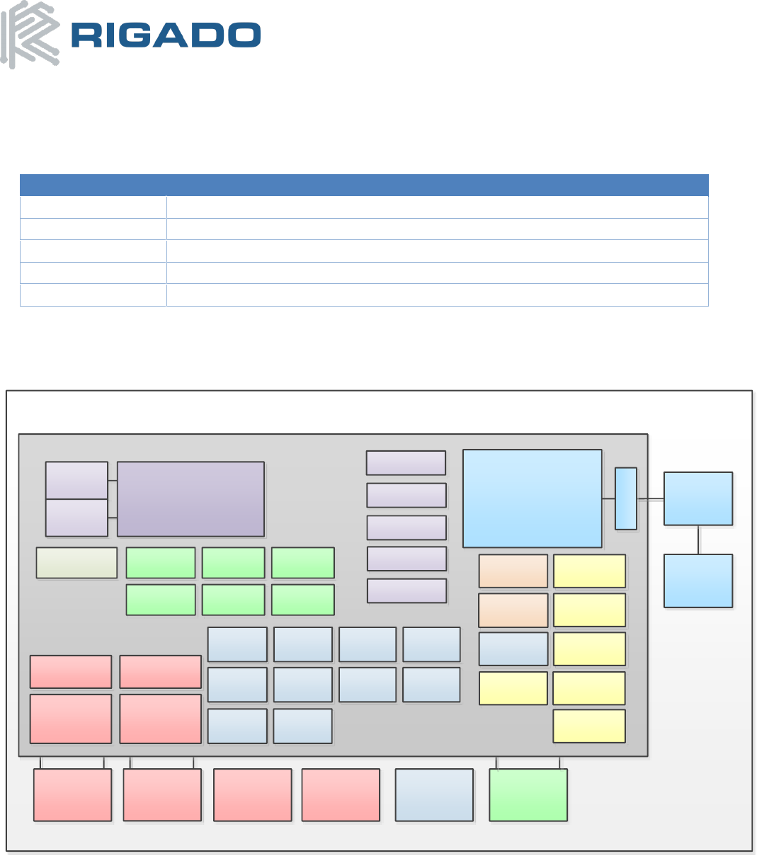
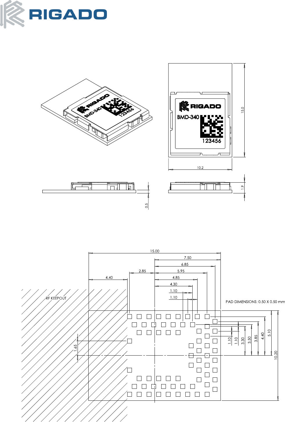
4. Block Diagram
BMD-340 Bluetooth 5 Low Energy SoC Module
32 MHz
Crystal
nRF52840-QIAA
1MB Flash
DC-DC
Inductor
Decoupling
Capacitors
Bulk
Capacitors
2.4GHz Radio
Multi-protocol
TWI
Master x2
SPI
Master x4
SPI Slave
x3
Core DC/DC
Buck Regulator
Core LDO
256kB
RAM
Low Power
Comparator
8-ch 12-bit
ADC
UART
x2 Quadrature
Decoder
SWD Debug &
Programming Temperature
Sensor
Cloc k
Management
Watchdog
Timer
Random Number
Gen
Timer x5
Accel Address
Resolver
AES CCM Mode
Encryption
AES ECB
Real Time
Counter x3
GPIO Task
Event Blocks
Programmable
Peripheral
Interconnect
ARM Cortex-M4F
@ 64MHz
Matching
Network
Internal
Trace
Antenna
GPIO x48
(Analog x8)
I2S
TWI Slave
x2
PWM
x4 PDM
General
Purpose
Comparator
NFC Tag
Balun
DC-DC
Inductor
5V DC/DC Buck
Regulator TWI Slave
x2 QSPI Master
w/XIP USB2.0
5V LDO
ARM CryptoCell
SW
Interrupts
Memory
Watch Unit
Figure 1 – Block Diagram

BMD-340 Module Datasheet
Bluetooth 5 + 802.15.4
May 21, 2018
BMD-340-DS V1.0 Page 3 of 31
Table of Contents
1. FEATURES ............................................................................................................................................................................... 1
2. APPLICATIONS ........................................................................................................................................................................ 1
3. ORDERING INFORMATION...................................................................................................................................................... 2
4. BLOCK DIAGRAM .................................................................................................................................................................... 2
5. QUICK SPECIFICATIONS .......................................................................................................................................................... 5
6. PIN DESCRIPTIONS ................................................................................................................................................................. 6
6.1 BMD-340 .............................................................................................................................................................................................. 6
6.2 PERIPHERAL PINS ...................................................................................................................................................................................... 8
6.3 BMD-300 SERIES FOOTPRINT COMPATIBILITY AND MIGRATION ....................................................................................................................... 9
6.3.1 BMD-300/301 to BMD-340 Pad Differences .................................................................................................................................. 10
6.3.2 BMD-300/301 to BMD-340 Design Migration ............................................................................................................................... 10
6.4 BMD-340 FANOUT EXAMPLE .................................................................................................................................................................. 11
7. ELECTRICAL SPECIFICATIONS ................................................................................................................................................ 12
7.1 ABSOLUTE MAXIMUM RATINGS ................................................................................................................................................................. 12
7.2 OPERATING CONDITIONS .......................................................................................................................................................................... 12
7.3 POWER AND DCDC CONFIGURATION ......................................................................................................................................................... 13
7.3.1 USB Power ....................................................................................................................................................................................... 13
7.3.2 Normal (LV) Power Mode Examples ............................................................................................................................................... 14
7.3.3 High Voltage (HV) Power Mode Examples ..................................................................................................................................... 15
7.4 GENERAL PURPOSE I/O ........................................................................................................................................................................... 16
7.5 MODULE RESET .................................................................................................................................................................................... 16
7.6 DEBUG & PROGRAMMING ........................................................................................................................................................................ 16
7.7 CLOCKS ................................................................................................................................................................................................. 17
8. FIRMWARE ........................................................................................................................................................................... 18
8.1 FACTORY IMAGE ..................................................................................................................................................................................... 18
8.2 SOFTDEVICES ......................................................................................................................................................................................... 18
8.2.1 S140 ................................................................................................................................................................................................. 18
8.3 IEEE 802.15.4 (THREAD AND ZIGBEE) ...................................................................................................................................................... 18
8.4 MAC ADDRESS INFO ............................................................................................................................................................................... 19
9. MECHANICAL DATA .............................................................................................................................................................. 20
9.1 MECHANICAL DIMENSIONS ....................................................................................................................................................................... 20
9.2 RECOMMENDED PCB LAND PADS .............................................................................................................................................................. 20
10. MODULE MARKING .............................................................................................................................................................. 21
11. RF DESIGN NOTES ................................................................................................................................................................. 21
11.1 RECOMMENDED RF LAYOUT & GROUND PLANE ........................................................................................................................................... 21
11.2 MECHANICAL ENCLOSURE......................................................................................................................................................................... 22
11.3 ANTENNA PATTERNS ............................................................................................................................................................................... 22
12. EVALUATION BOARDS .......................................................................................................................................................... 23
13. EDGE CONNECTIVITY SOLUTIONS ......................................................................................................................................... 23
14. BLUETOOTH QUALIFICATION ................................................................................................................................................ 24
15. REGULATORY STATEMENTS .................................................................................................................................................. 24
15.1 FCC STATEMENT: ................................................................................................................................................................................... 24
15.2 FCC IMPORTANT NOTES .......................................................................................................................................................................... 24
15.3 IC STATEMENT: ...................................................................................................................................................................................... 26
15.4 IC IMPORTANT NOTES ............................................................................................................................................................................. 26
15.5 CE REGULATORY ..................................................................................................................................................................................... 27
15.6 AUSTRALIA / NEW ZEALAND ..................................................................................................................................................................... 27
16. SOLDER REFLOW TEMPERATURE-TIME PROFILE ................................................................................................................... 28
16.1 MOISTURE SENSITIVITY LEVEL.................................................................................................................................................................... 28
17. PACKAGING AND LABELING .................................................................................................................................................. 28
17.1 CARRIER TAPE DIMENSIONS ...................................................................................................................................................................... 28
17.2 REEL PACKAGING .................................................................................................................................................................................... 29
17.3 PACKAGING LABEL ................................................................................................................................................................................... 29
18. CAUTIONS ............................................................................................................................................................................ 30
19. LIFE SUPPORT POLICY ........................................................................................................................................................... 30
20. DOCUMENT HISTORY ........................................................................................................................................................... 31
21. RELATED DOCUMENTS ......................................................................................................................................................... 31

BMD-340 Module Datasheet
Bluetooth 5 + 802.15.4
May 21, 2018
BMD-340-DS V1.0 Page 4 of 31
List of Figures
FIGURE 1 – BLOCK DIAGRAM ............................................................................................................................................................ 2
FIGURE 2 – BMD-340 PIN OUT (TOP VIEW) ........................................................................................................................................ 6
FIGURE 3 – BMD-340 AND BMD-300/301 FOOTPRINT COMPARISON .................................................................................................... 9
FIGURE 4 – BMD-300 MODULE SOLDERED TO BMD-340 FOOTPRINT...................................................................................................... 9
FIGURE 5 – BMD-300 TO BMD-340 MIGRATION EXAMPLE................................................................................................................. 10
FIGURE 6 – BMD-340 2 LAYER FANOUT EXAMPLE .............................................................................................................................. 11
FIGURE 7 – LV MODE W/ COIN CELL EXAMPLE ................................................................................................................................... 14
FIGURE 8 – LV MODE EXAMPLE W/ USB AND EXTERNAL REGULATOR ...................................................................................................... 14
FIGURE 9 – USB POWERED HV MODE EXAMPLE ................................................................................................................................ 15
FIGURE 10 – LIPO POWERED HV EXAMPLE W/ USB CHARGER ............................................................................................................... 15
FIGURE 11 – BMD-340 MAC ADDRESS ON LABEL.............................................................................................................................. 19
FIGURE 12 – BMD-340 MODULE DIMENSIONS.................................................................................................................................. 20
FIGURE 13 – BMD-340/301 DIMENSIONS (TOP VIEW) ...................................................................................................................... 20
FIGURE 14 – BMD-340 MODULE MARKING - REV 1 (ES1) .................................................................................................................. 21
FIGURE 15 – BMD-340 RF EXAMPLE BASED ON EVAL BOARD .............................................................................................................. 21
FIGURE 16 – X-Y-Z ANTENNA ORIENTATION ...................................................................................................................................... 22
FIGURE 17 – BMD-340 EVALUATION BOARD .................................................................................................................................... 23
FIGURE 18 – REFLOW PROFILE FOR LEAD FREE SOLDER ......................................................................................................................... 28
FIGURE 19 - BMD-340 TAPE DIMENSIONS ....................................................................................................................................... 28
FIGURE 20 – REEL PACKAGING ........................................................................................................................................................ 29
FIGURE 21 – PACKAGING LABEL....................................................................................................................................................... 29
List of Tables
TABLE 1 – ORDERING PART NUMBERS ................................................................................................................................................ 2
TABLE 2 – QUICK SPECIFICATIONS ...................................................................................................................................................... 5
TABLE 3 – BMD-340 PIN DESCRIPTIONS ............................................................................................................................................ 7
TABLE 4 – PERIPHERAL PIN OPTIONS .................................................................................................................................................. 8
TABLE 5 – PERIPHERALS WITH SHARED REGISTERS.................................................................................................................................. 8
TABLE 6 – BMD-300/301 TO BMD-340 PAD DIFFERENCES ................................................................................................................ 10
TABLE 9 – ABSOLUTE MAXIMUM RATINGS ......................................................................................................................................... 12
TABLE 10 – OPERATING CONDITIONS ................................................................................................................................................ 12
TABLE 11 – POWER MODE PIN CONNECTIONS .................................................................................................................................... 13
TABLE 12 – GPIO ........................................................................................................................................................................ 16
TABLE 13 – 32.768 KHZ CRYSTAL ................................................................................................................................................... 17
TABLE 14 – 32.768 KHZ OSCILLATOR............................................................................................................................................... 17

BMD-340 Module Datasheet
Bluetooth 5 + 802.15.4
May 21, 2018
BMD-340-DS V1.0 Page 5 of 31
5. Quick Specifications
Bluetooth
Version
5.0 (Bluetooth Smart) Concurrent Central & Peripheral (S140)
Security
AES-128
LE connections
Up to 8 as Central, 1 as Peripheral, Observer, Broadcaster (S140)
IEEE 802.15.4
Thread Stack
OpenThread, Thread 1.1 certified
Thread Security
AES-128, ARM® Cryptocell accelerated
Zigbee Stack
Zigbee 3.0 (Certification Pending)
Radio
Frequency
2.402GHz to 2.480GHz
Modulations
GFSK at 1 Mbps and 2Mbps, QPSK at 250kbps
Transmit power
+8 dBm
Receiver sensitivity
-93dBm (2Mbps), -96 dBm (1Mbps), -103 (125ksps BLE), -100 dBm (IEEE 802.15.4)
Antenna
Integrated
Current Consumption
TX only @ +8 dBm, 0 dBm @ 3V, DCDC enabled
14.8 mA, 4.8 mA
TX only @ +8 dBm, 0 dBm
32.7 mA, 10.6 mA
RX only @ 1 Mbps @ 3V, DCDC enabled
4.6 mA
RX only @ 1 Mbps
9.9 mA
CPU @ 64MHz from flash, from RAM
6.3 mA, 5.2mA
CPU @ 64MHz from flash, from RAM @ 3V, DCDC enabled
3.3 mA, 2.8mA
System Off, On (Supply on VDD), no RAM retention
0.4 µA, 0.97 µA
System Off, On (Supply on VDD), full 256kB RAM retention
1.86 µA, 2.35µA
Dimensions
BMD-340
Length
Width
Height
15.0 mm ± 0.3mm
10.2 mm ± 0.3mm
1.9 mm ± 0.1mm
Hardware
Interfaces
SPI Master/Slave x4
Quad SPI x1
UART x2
Two-Wire Master/Slave (I2C) x2
GPIO x48
I2S x1
PWM x12
PDM x1
USB 2.0 x1
Analog input x8
Power supply
VDD: 1.7V to 3.6V, 1.75V required to start DCDC
VDDH: 2.5V to 5.5V
VBUS: 4.35V to 5.5V (For USB operation)
Temperature Range
-40 to +85°C
Certifications
FCC
FCC part 15 modular certification
BMD-340 FCC ID: 2AA9B10
IC
Industry Canada RSS-247 modular certification
BMD-340 IC: 12208A-10
CE
EN 301 489-1 V2.1.1& 3.1 (b): Electromagnetic Compatibility
EN 301 489-17 V3.1.1
EN 300 328 V2.1.1 3.2: Effective use of spectrum allocated
Australia / New Zealand
AS/NZS 4268 :2012+AMDT 1:2013, Radio equipment and systems – Short range devices
Bluetooth
BMD-340 RF-PHY Component (Tested) – DID: TBD; QDID: TBD
Table 2 – Quick Specifications
BMD-340 Module Datasheet
Bluetooth 5 + 802.15.4
May 21, 2018
BMD-340-DS V1.0 Page 6 of 31
6. Pin Descriptions
6.1 BMD-340
Figure 2 – BMD-340 Pin out (Top View)
Pin description
Pin
Name
Direction
Description
6
P0.25
In/Out
GPIO
7
P0.26
In/Out
GPIO
8
P0.27
In/Out
GPIO
9
P0.28
In/Out
GPIO/AIN42
10
P0.29
In/Out
GPIO/AIN52
11
P0.30
In/Out
GPIO/AIN62
12
P0.31
In/Out
GPIO/AIN72
13
P0.00
In/Out
GPIO/XTAL1 (32.768kHz)
14
P0.01
In/Out
GPIO/XTAL2 (32.768kHz)
15
P0.02
In/Out
GPIO/AIN02
19
P0.03
In/Out
GPIO/AIN12
20
P0.04
In/Out
GPIO/AIN2
21
P0.05
In/Out
GPIO/AIN3
22
P0.06
In/Out
GPIO
23
P0.07
In/Out
GPIO/TRACECLK
24
P0.08
In/Out
GPIO
25
P0.09
In/Out
GPIO/NFC12
26
P0.10
In/Out
GPIO/NFC22
27
P0.11
In/Out
GPIO/TRACEDATA[2]
28
P0.12
In/Out
GPIO/TRACEDATA[1]
31
P0.13
In/Out
GPIO
32
P0.14
In/Out
GPIO

BMD-340 Module Datasheet
Bluetooth 5 + 802.15.4
May 21, 2018
BMD-340-DS V1.0 Page 7 of 31
Pin
Name
Direction
Description
33
P0.15
In/Out
GPIO
34
P0.16
In/Out
GPIO
35
P0.17
In/Out
GPIO
36
P0.21
In/Out
GPIO
37
P0.19
In/Out
GPIO
38
P0.20
In/Out
GPIO
39
P0.18
In/Out
GPIO/RESET
̅
̅
̅
̅
̅
̅
̅
̅
40
P0.22
In/Out
GPIO
41
P0.23
In/Out
GPIO
42
P0.24
In/Out
GPIO
43
SWCLK
In
SWD Clock
44
SWDIO
In/Out
SWD IO
48
P1.05
In/Out
GPIO2
49
P1.06
In/Out
GPIO2
50
P1.07
In/Out
GPIO2
51
P1.08
In/Out
GPIO
52
P1.09
In/Out
GPIO/TRACEDATA[3]
53
P1.10
In/Out
GPIO2
54
P1.11
In/Out
GPIO2
56
P1.00
In/Out
GPIO/TRACEDATA[0]/SWO
57
P1.01
In/Out
GPIO2
58
P1.02
In/Out
GPIO2
59
P1.03
In/Out
GPIO2
60
P1.04
In/Out
GPIO2
61
P1.12
In/Out
GPIO2
62
P1.13
In/Out
GPIO2
63
P1.14
In/Out
GPIO2
64
P1.15
In/Out
GPIO2
67
USB-D-
In/Out
USB Data -
68
USB-D+
In/Out
USB Data +
66
VBUS
Power
USB PHY supply: 4.35V to 5.5V in
Connect to USB Host device 5V supply
17
VCC1
Power In/Out
LV Mode: 1.7V to 3.6V in
HV Mode: 1.8V to 3.3V supply out3
65
VCCH1
Power
LV Mode: Connect to VCC
HV Mode: 2.5V to 5.5V in
1, 2, 3, 4, 5, 16, 18, 29, 30,
45, 46, 47, 55
GND
Power
Electrical Ground
Note 1: An internal 4.7µF bulk capacitor is included on the module. However, it is good design practice to add additional bulk
capacitance as required for your application, i.e. those with heavy GPIO usage and/or current draw.
Note 2: These pins are in close proximity to the nRF52 radio power supply and antenna pins. Radio performance parameters, such
as sensitivity, may be affected by high frequency digital I/O with large sink/source current on these pins. Nordic recommends using
only low frequency, low-drive functions when possible.
Note 3: In HV mode, VCC acts as a regulated supply that can power other external devices. The voltage output of VCC can be
configured in software but is limited to no more than VCCH-0.3V. In System Off mode VCC can supply no more than 1mA.
Table 3 – BMD-340 Pin Descriptions

BMD-340 Module Datasheet
Bluetooth 5 + 802.15.4
May 21, 2018
BMD-340-DS V1.0 Page 8 of 31
6.2 Peripheral Pins
The BMD-340 features a pin muxing system that allows most internal peripherals, such as UART and SPI, to be
used on any GPIO pin. This freedom in pin choice enables better optimization of designs and PCB layout. Note that
only one peripheral signal can be muxed to a GPIO pin at a time. Some functions are restricted to certain pins due
to additional internal circuitry required by the interface. These include: Trace signals, analog inputs, XTAL signals,
USB signals, SWD interface, and reset. See Table 4 below for details:
Peripheral
Signal
Pin Options
UART0, UART1
All
P0.00-P0.31, P1.00-P1.15
I2C0, I2C1
SPI0, SPI1, SPI2, SPI3
I2S0
QSPI0
PWM0, PWM1, PWM2, PWM3
PDN0
ADC, COMP, LPCOMP
All
P0.02-P0.05, P0.28-P0.31
(AIN0-AIN7)
NFC
NFC1
P0.09
NFC2
P0.10
Reset
RESET
̅
̅
̅
̅
̅
̅
̅
̅
P0.18
Trace
TRACECLK
P0.07
SWO/TRACEDATA[0]
P1.00
TRACEDATA[1]
P0.12
TRACEDATA[2]
P0.11
TRACEDATA[3]
P1.09
SWD
SWD Clock
SWCLK
SWD IO
SWDIO
32.768kHz Crystal
XTAL1
P0.00
XTAL2
P0.01
USB
USB Data +
USB-D+
USB Data -
USB-D-
Table 4 – Peripheral Pin Options
Note: Some peripherals on the BMD-340 share the same memory location for their registers. This means that only
one of these peripherals can be used at a time. It is possible to switch between peripherals that share the same
register location by clearing and reinitializing the associated configuration registers. See the Nordic Semiconductor
nRF52840 Product Specification for details.
Peripheral
ID
Base Address
Shared Peripherals
3
0x40003000
SPI0
I2C0
4
0x40004000
SPI1
I2C1
Table 5 – Peripherals with Shared Registers
BMD-340 Module Datasheet
Bluetooth 5 + 802.15.4
May 21, 2018
BMD-340-DS V1.0 Page 9 of 31
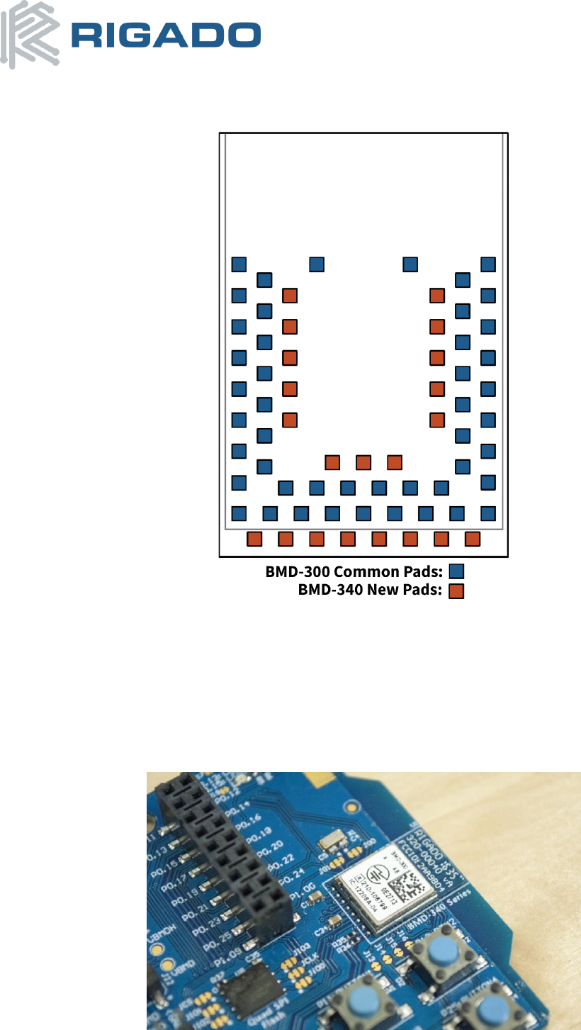
6.3 BMD-300 Series Footprint Compatibility and Migration
Figure 3 – BMD-340 and BMD-300/301 Footprint Comparison
The BMD-340 footprint has been designed to allow for backwards compatibility with the BMD-300 and BMD-301
modules with pins 1 through 47 of the BMD-340 directly mapping to the same pin numbers on the BMD-300/300.
This allows BMD-300 and BMD-301 modules to be placed directly onto the BMD-340 footprint for easy migration
and enabling tiered product design. Generally, all pin names and functions remain the same, except for some
differences noted below. Pins 48 through 68 of the BMD-340 footprint are new pads used for new features that
are not present on the BMD-300/301 modules, such as USB interface and additional GPIO and power connections.
Figure 4 – BMD-300 Module Soldered to BMD-340 Footprint
BMD-340 Module Datasheet
Bluetooth 5 + 802.15.4
May 21, 2018
BMD-340-DS V1.0 Page 10 of 31
6.3.1 BMD-300/301 to BMD-340 Pad Differences
Due to changes in the nRF52840 SoC used by the BMD-340, not all functions (such as SWO/TRACE signals) are
found on the same pins as on the BMD-300/301. Particularly of note is the reset pin function which on the BMD-
340 is now available on P0.18 instead of P0.21 as on the BMD-300/301. To maintain pin for pin compatibility of
the reset signal, P0.18 and P0.21 have swapped pad locations on the BMD-340 footprint. These differences are
detailed in Table 6 below:
Pin
BMD-300/301
Name
BMD-300/301
Function
BMD-340
Name
BMD-340
Function
39
P0.21
GPIO/RESET
̅
̅
̅
̅
̅
̅
̅
̅
P0.18
GPIO/RESET
̅
̅
̅
̅
̅
̅
̅
̅
38
P0.20
GPIO/TRACECLK
P0.20
GPIO
36
P0.18
GPIO/TRACEDATA[0]/SWO
P0.21
GPIO
34
P0.16
GPIO/TRACEDATA[1]
P0.16
GPIO
33
P0.15
GPIO/TRACEDATA[2]
P0.15
GPIO
32
P0.14
GPIO/TRACEDATA[3]
P0.14
GPIO
23
P0.07
GPIO
P0.07
GPIO/TRACECLK
56
N/A
N/A
P1.00
GPIO/TRACEDATA[0]/SWO
28
P0.12
GPIO
P0.12
GPIO/TRACEDATA[1]
27
P0.11
GPIO
P0.11
GPIO/TRACEDATA[2]
52
N/A
N/A
P1.09
GPIO/TRACEDATA[3]
Table 6 – BMD-300/301 to BMD-340 Pad Differences
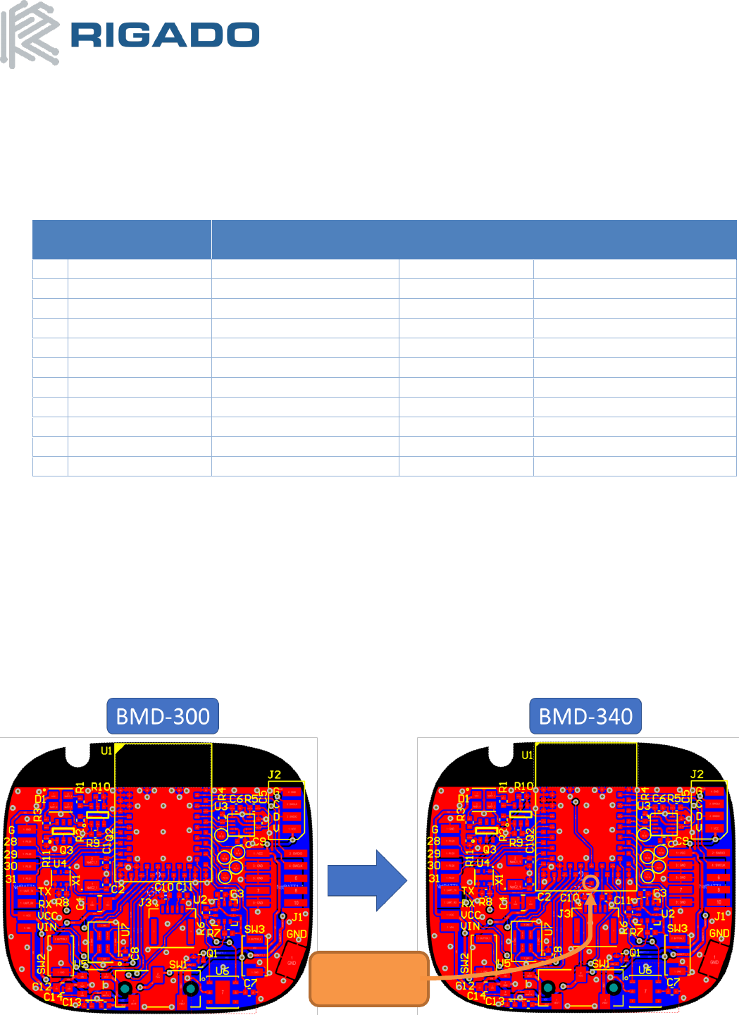
6.3.2 BMD-300/301 to BMD-340 Design Migration
Existing designs incorporating the BMD-300 or BMD-301 module can be migrated over to the BMD-340 with the
addition of a single footprint pad for VCCH (pin 65). This migration option is only suitable for applications that do
not require the new USB interface, additional GPIO, or higher supply voltage functionality. The VCCH pad must be
present and electrically connected to the same supply as VCC in order for the module to operate correctly. Vias
underneath the BMD-340 should be tented to avoid shorts to unused module pads. Firmware written for the
BMD-300/301 can generally be ported to the BMD-340 with minimal effort. See the Nordic Semiconductor SDK
documentation for details.
Figure 5 – BMD-300 to BMD-340 Migration Example
New Pad VCCH:
Connect to VCC
BMD-340 Module Datasheet
Bluetooth 5 + 802.15.4
May 21, 2018
BMD-340-DS V1.0 Page 11 of 31
Using the BMD-340 minimal footprint, with only the additional VCCH pad added, allows BMD-300 designs to gain
the following BMD-340 features with typically minor layout re-work:
• Bluetooth 5 long range modes
• IEEE 802.15.4 (Thread and Zigbee) connectivity
• Doubled Flash memory (1MB vs. 512kB)
• Quadrupled RAM (256kB vs. 64kb)
• ARM® TrustZone® Cryptocell 310 security co-processor
To take advantage of new hardware features, such as the additional UART and Quad SPI interface, the full BMD-
340 footprint should be used. Designs that require the 5V DCDC converter, trace interface, USB interface, or the
additional GPIO (P1.00-P1.15) must use the full BMD-340 footprint.
Note: Since the BMD-300 can be soldered to the full BMD-340 footprint, it is highly recommended that all new
BMD-300 and BMD-340 projects use the full BMD-340 footprint. When migrating designs, the full BMD-340
footprint should be used whenever possible as it is better suited for use with mass production SMT processing.
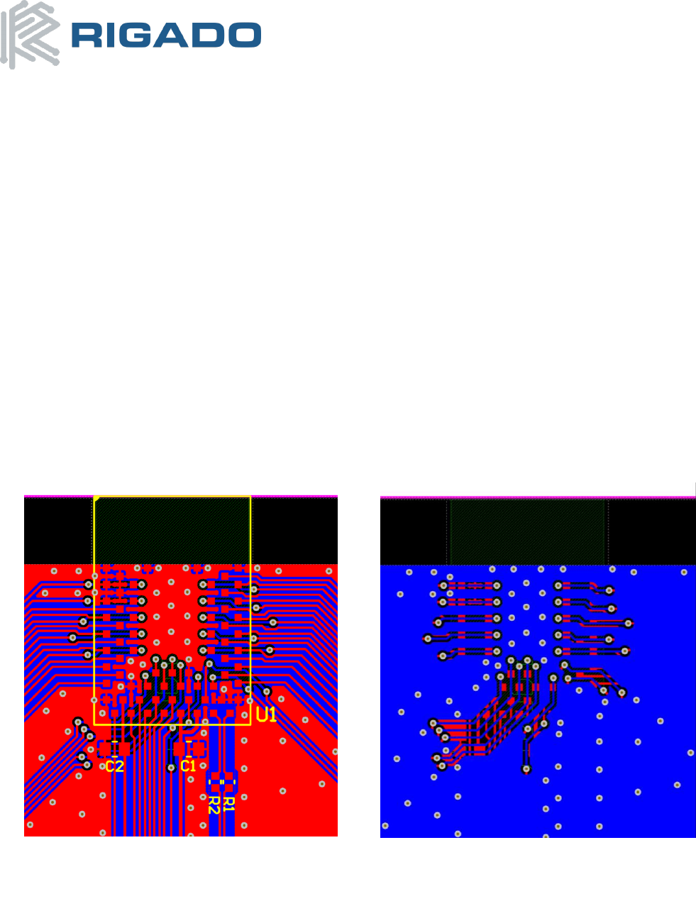
6.4 BMD-340 Fanout Example
The following figure is a BMD-340 fanout example on a simple 2-layer PCB. This example is powered via VCCH
from a USB connection. See Section 7.3 for details on power and DCDC operation.
Figure 6 – BMD-340 2 Layer Fanout Example
Top Layer
Bottom Layer
BMD-340 Module Datasheet
Bluetooth 5 + 802.15.4
May 21, 2018
BMD-340-DS V1.0 Page 12 of 31
7. Electrical Specifications
7.1 Absolute Maximum Ratings
Symbol
Parameter
Min.
Max.
Unit
VCC_MAX
Voltage on VCC supply pin
-0.3
3.9
V
VCCH_MAX
Voltage on VCCH supply pin
-0.3
5.8
V
VBUS_MAX
Voltage on VBUS Supply pin
-0.3
5.8
V
VIO_MAX
Voltage on GPIO pins (VCC > 3.6V)
-0.3
3.9
V
VIO_MAX
Voltage on GPIO pins (VCC ≤ 3.6V)
-0.3
VCC + 0.3V
V
TS
Storage Temperature Range
-40
125
°C
Table 7 – Absolute Maximum Ratings
7.2 Operating Conditions
Symbol
Parameter
Min.
Typ.
Max.
Unit
VCC_IN
VCC operating supply voltage in
1.7
3.0
3.6
V
VCC_START
VCC DCDC starting voltage
1.75
-
-
V
VCCH_HV
VCCH operating supply voltage in
2.5
5.0
5.5
V
VBUS_IN
VBUS operating supply voltage in
4.35
5.0
5.5
V
TR_VCC
VCC Supply rise time (0V to 1.7V)
-
-
60
ms
TR_VCCH
VCCH Supply rise time (0V to 3.7V)1
-
-
1
ms
TA
Operating Ambient Temperature Range
-40
25
85
°C
Note 1: Applies when module is configured to use HV mode. When using LV mode TR_VCC applies. See Nordic nRF52840
Rev 1 errata [202] for details on TR_VCCH requirement.
Table 8 – Operating Conditions

BMD-340 Module Datasheet
Bluetooth 5 + 802.15.4
May 21, 2018
BMD-340-DS V1.0 Page 13 of 31
7.3 Power and DCDC Configuration
Important Note Regarding REG0: Initial mass production silicon (Nordic Rev 1) for the nRF52840 includes some
errata that affect the REG0 regulator. The REG0 DC-DC converter mode cannot be used reliably. The LDO mode of
REG0 can be used in High Voltage mode but when applying power the input voltage must have a rise time of 1ms
or less. Due to the rise time constraint and higher current consumption of LDO mode compared to DCDC, High
Voltage mode should be considered non-functional for most applications and should not be used on ES2 and
Revision A BMD-340 modules. See Nordic nRF52840 errata 197 and 202 for more details. These errata are
expected to be corrected in future production silicon releases and subsequent revisions of the BMD-340 module.
Contact Rigado for timing and details.
The BMD-340 has two internal regulator stages that each contain an LDO and DCDC regulator. The first regulator,
REG0, is fed by the VCCH pin and can accept a source voltage of 2.5V to 5.5V. The output of REG0 is connected to
the VCC pin and the input of the second regulator stage REG1. REG1 supplies power to the module core and can
accept an input source voltage of 1.7V to 3.6V. Depending on how the VCC and VCCH pins are connected, the
module will operate in one of two modes: Normal/Low Voltage (LV) or High Voltage (HV). The voltage present on
the VCC pin is always the GPIO high logic level voltage, regardless of power mode.
To enter LV Mode, the same source voltage is applied to both the VCC and VCCH pins causing REG0 to
automatically shut down leaving only the REG1 stage active. To enter HV, the source voltage is only applied to
VCCH causing the VCC pin to become an output source supplied by REG0.
Mode
Pin
Name
Connection
Normal (LV)
17
VCC
1.7V to 3.6V source in
65
VCCH
Same source as VCC
High Voltage (HV)
17
VCC
1.8V to 3.3V supply out
65
VCCH
2.5V to 5.5V source in
Table 9 – Power Mode Pin Connections
Important: in both LV and HV mode, the GPIO logic level voltage is determined by the VCC pin. In HV mode, all
external devices that are connected to the BMD-340’s GPIO must either be powered by the module (from VCC) or
use level translation.
REG0 can supply a maximum current of ~50mA for the module and external circuits in System On Mode and 1mA
in System Off Mode. External circuits powered from VCC in HV mode should be limited to no more than 20mA to
ensure stability.
7.3.1 USB Power
The USB interface on the BMD-340 can be used when the module is in either Normal (LV) or High Voltage (HV)
mode. The BMD-340 USB PHY is powered by a dedicated, internal LDO regulator that is fed by the VBUS pin (66).
This means that applying power to only the VBUS pin will not power the rest of the module. In order for the USB
PHY to operate, VBUS must be externally powered.
BMD-340 Module Datasheet
Bluetooth 5 + 802.15.4
May 21, 2018
BMD-340-DS V1.0 Page 14 of 31
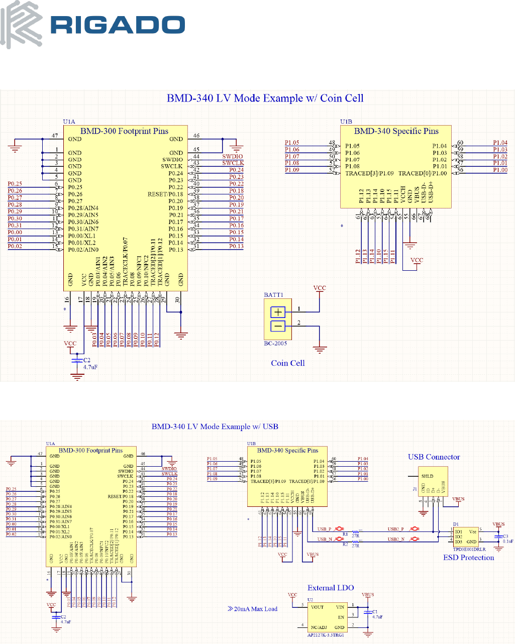
7.3.2 Normal (LV) Power Mode Examples
Figure 7 – LV Mode w/ Coin Cell Example
Figure 8 – LV Mode Example w/ USB and External Regulator
BMD-340 Module Datasheet
Bluetooth 5 + 802.15.4
May 21, 2018
BMD-340-DS V1.0 Page 15 of 31
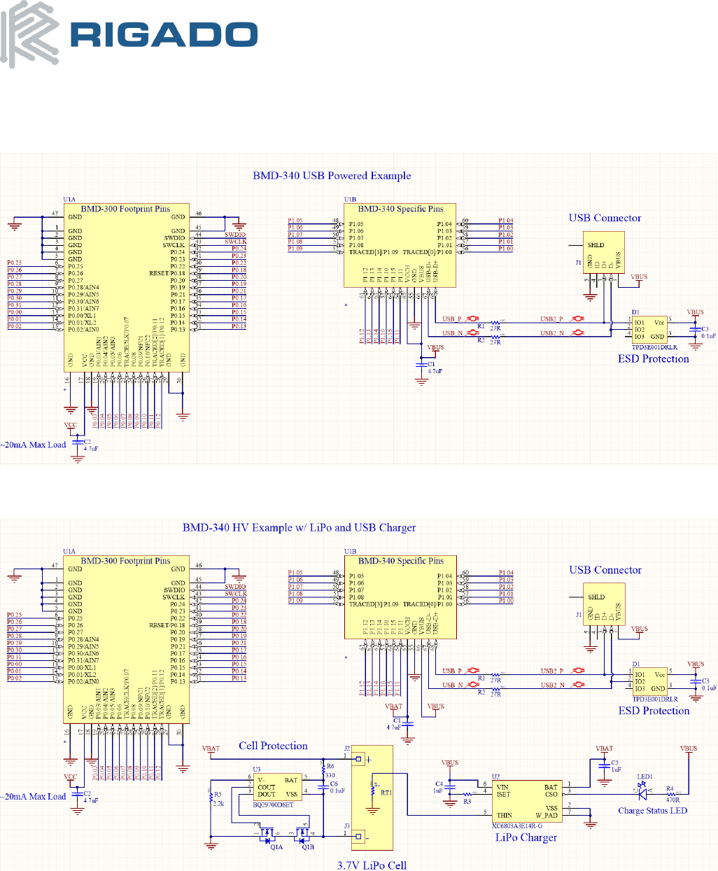
7.3.3 High Voltage (HV) Power Mode Examples
Figure 9 – USB Powered HV Mode Example
Figure 10 – LiPo Powered HV Example w/ USB Charger
Important: the LiPo circuit above is meant to be a generic example of how the BMD-340’s power modes can be
used. Great care must be taken when integrating Lithium-Ion batteries into a design. Protection circuits suitable
for the type of battery used and the application must always be implemented.

BMD-340 Module Datasheet
Bluetooth 5 + 802.15.4
May 21, 2018
BMD-340-DS V1.0 Page 16 of 31
7.4 General Purpose I/O
The general purpose I/O is organized as two ports enabling access and control of the 48 available GPIO pins. The
first port allows access of P0.00 to P0.31, similar to the one port available on the BMD-300/301. The second port,
new to the BMD-340, allows access to P1.00 to P1.15. Each GPIO can be accessed individually with the following
user configurable features:
• Input/output direction
• Output drive strength
• Internal pull-up and pull-down resistors
• Wake-up from high or low level triggers on all pins
• Trigger interrupt on all pins
• All pins can be used by the PPI task/event system; the maximum number of pins that can be interfaced
through the PPI at the same time is limited by the number of GPIOTE channels
• All pins can be individually configured to carry serial interface or quadrature demodulator signals
Symbol
Parameter
Min.
Typ.
Max.
Unit
VIH
Input High Voltage
0.7 x VCC
-
VCC
V
VIL
Input Low Voltage
VSS
-
0.3 x VCC
V
VOH
Output High Voltage
VCC − 0.4
-
VCC
V
VOL
Output Low Voltage
VSS
-
VSS + 0.4
V
RPU
Pull-up Resistance
11
13
16
kΩ
RPD
Pull-down Resistance
11
13
16
kΩ
Table 10 – GPIO
7.5 Module RESET
GPIO pin P0.18 may be used for a hardware reset. In order to utilize P0.18 as a hardware reset, the UICR registers
PSELRESET[0] and PSELRESET[1] must be set alike, to the value of 0x7FFFFFD2. When P0.18 is programmed as
RESET
̅
̅
̅
̅
̅
̅
̅
̅
, the internal pull-up is automatically enabled. Rigado and Nordic example applications and development
kits program P0.18 as RESET
̅
̅
̅
̅
̅
̅
̅
̅
.
7.6 Debug & Programming
The BMD-340 supports the two pin Serial Wire Debug (SWD) interface and offers flexible and powerful
mechanisms for non-intrusive debugging of program code. Breakpoints, single stepping, and instruction trace
capture of code execution flow are part of this support.
The BMD-340 also supports ETM and ITM trace. Trace data from the ETM and the ITM is sent to an external
debugger via a 4-bit wide parallel trace port. In addition to parallel trace, the TPIU supports serial trace via the
Serial Wire Output (SWO) trace protocol.

BMD-340 Module Datasheet
Bluetooth 5 + 802.15.4
May 21, 2018
BMD-340-DS V1.0 Page 17 of 31
7.7 Clocks
The BMD-340 requires two clocks, a high frequency clock and a low frequency clock.
The high frequency clock is provided on-module by a high-accuracy 32-MHz crystal as required by the
nRF52840 for radio operation.
The low frequency clock can be provided internally by an RC oscillator or synthesized from the fast clock; or
externally by a 32.768 kHz crystal. An external crystal provides the lowest power consumption and greatest
accuracy. Using the internal RC oscillator with calibration provides acceptable performance for BLE
applications at a reduced cost and slight increase in power consumption. Note: the ANT protocol requires the
use of an external crystal.
32.768 kHz Crystal (LFXO)
Symbol
Parameter
Typ.
Max.
Unit
FNOM_LFXO
Crystal frequency
32.768
-
kHz
FTOL_LFXO_BLE
Frequency tolerance, BLE applications
-
±250
ppm
CL_LFXO
Load Capacitance
-
12.5
pF
C0_LFXO
Shunt Capacitance
-
2
pF
RS_LFXO
Equivalent series resistance
-
100
kΩ
Cpin
Input Capacitance on XL1 & XL2 pads
4
-
pF
Table 11 – 32.768 kHz Crystal
32.768 kHz Oscillator Comparison
Symbol
Parameter
Min.
Typ.
Max.
Unit
ILFXO
Current for 32.768kHz Crystal Oscillator
-
0.23
-
µA
ILFRC
Current for 32.768kHz RC Oscillator
-
0.7
1
µA
ILFSYNT
Current for 32.768kHz Synthesized Oscillator
-
100
-
µA
fTOL_LFXO_BLE
Frequency Tolerance, 32.768kHz Crystal Oscillator
(BLE Stack)1
-
-
±250
ppm
fTOL_LFXO_ANT
Frequency Tolerance, 32.768kHz Crystal Oscillator
(ANT Stack)1
-
-
±50
ppm
f TOL_LFRC
Frequency Tolerance, 32.768kHz RC Oscillator
-
-
±2
%
fTOL_CAL_LFRC
Frequency tolerance, 32.768kHz RC after calibration
-
-
±250
ppm
fTOL_LFSYNT
Frequency Tolerance, 32.768kHz Synthesized
Oscillator
-
-
±48
ppm
Note 1: fTOL_LFXO_BLE and fTOL_LFXO_ANT are the max allowed for BLE and ANT applications. Actual tolerance depends
on the crystal used.
Table 12 – 32.768 kHz Oscillator

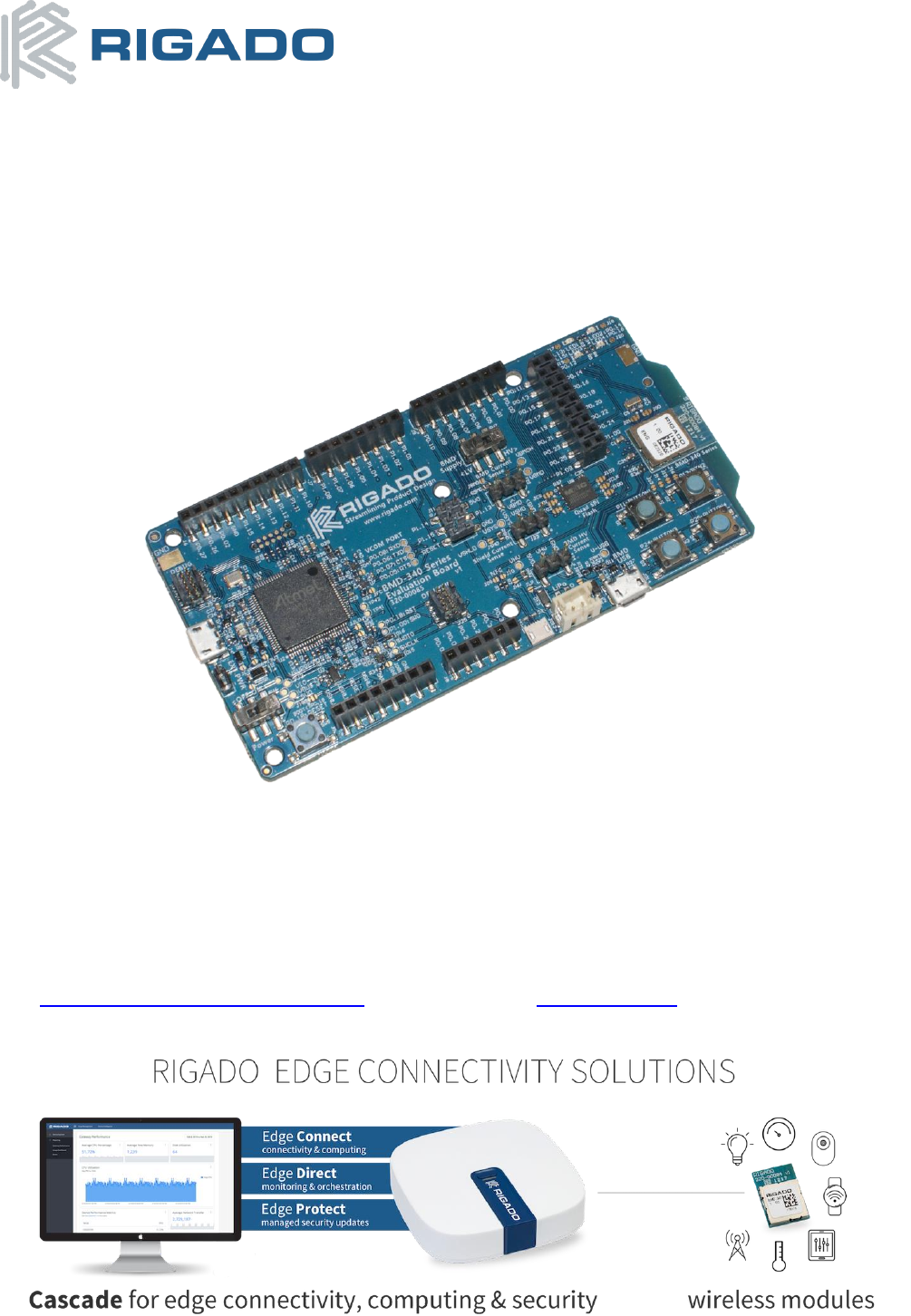
BMD-340 Module Datasheet
Bluetooth 5 + 802.15.4
May 21, 2018
BMD-340-DS V1.0 Page 18 of 31
8. Firmware
8.1 Factory Image
The BMD-340 module is not loaded with a factory firmware image. The unique Rigado MAC address printed on
the module label and is also programmed into the UICR.
8.2 SoftDevices
Nordic Semiconductor protocol stacks for Bluetooth and ANT are known as SoftDevices. SoftDevices are pre-
compiled, pre-linked binary files. SoftDevices can be programmed in nRF52 series SoCs and are downloadable
from the Nordic website. The BMD-340 with the nRF52840 SoC supports the S140 (BLE Central & Peripheral)
SoftDevice.
8.2.1 S140
The S140 SoftDevice is a Bluetooth® low energy (BLE) Central and Peripheral protocol stack solution
supporting up to eight connections with an additional Observer and a Broadcaster role all running
concurrently. The S140 SoftDevice integrates a BLE Controller and Host, and provides a full and flexible API for
building Bluetooth Smart nRF52 System on Chip (SoC) solutions. The S140 Softdevice is an extension of the
S132 V3.0 Softdevice adding support for Bluetooth 5.
Key Features
• Bluetooth 5 compliant low energy single-mode protocol
stack suitable for Bluetooth Smart products
• Concurrent Central, Observer, Peripheral, and
Broadcaster roles with up to eight concurrent
connections along with one observer and one
broadcaster
o Configurable number of connections and
bandwidth per connection to optimize memory and
performance
o Configurable attribute table size
o Custom UUID support
o Link layer
o LL Privacy
o LE Data Packet Length Extension
o L2CAP, ATT, and SM protocols
o LE Secure Connections pairing model
o GATT and GAP APIs
o GATT Client and Server
o Configurable ATT MTU
• Complementary nRF5 SDK including Bluetooth profiles
and example applications
• Master Boot Record for over-the-air device firmware
update
o SoftDevice, application, and bootloader can be
updated separately
• Memory isolation between the application and the
protocol stack for robustness and security
• Thread-safe supervisor-call based API
• Asynchronous, event-driven behavior
• No RTOS dependency
o Any RTOS can be used
• No link-time dependencies
o Standard ARM® Cortex®-M4 project configuration
for application development
• Support for concurrent and non-concurrent
multiprotocol operation
o Concurrent with the Bluetooth stack using Radio
Timeslot API
o Alternate protocol stack in application space
• Support for control of external Power Amplifiers and
Low Noise Amplifiers
8.3 IEEE 802.15.4 (Thread and Zigbee)
IEEE 802.15.4 based protocols, such as Thread and Zigbee, on the BMD-340 are not implemented using a
Softdevice. Nordic Semiconductor provides an IEEE 802.15.4 compliant MAC stack which does not require a
Softdevice to be loaded to operate. Nordic Semiconductor also provides pre-compiled Thread and Zigbee
stacks. See developer.nordicsemi.com/nRF5_SDK/doc/ for more information on developing applications that
utilize IEEE 802.15.4.
BMD-340 Module Datasheet
Bluetooth 5 + 802.15.4
May 21, 2018
BMD-340-DS V1.0 Page 19 of 31
8.4 MAC Address Info
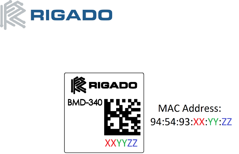
The BMD-340 modules comes preprogrammed with a unique MAC address from the factory. The MAC
address is also printed on a 2D barcode on the top of the module.
Figure 11 – BMD-340 MAC Address on Label
The 6-byte BLE Radio MAC address is stored in the nRF52840 UICR at NRF_UICR_BASE+0x80 LSB first. Please
read the MAC Address Provisioning application note if you are not using the built in bootloader to avoid
erasing/overwriting the MAC address during programming. Important: If full memory protection is enabled,
the UICR cannot be read via the SWD interface. If performing a full-erase, the MAC can then only be recovered
from the 2D barcode and human-readable text.
UICR Register:
NRF_UICR + 0x80 (0x10001080): MAC_Addr [0] (0xZZ)
NRF_UICR + 0x81 (0x10001081): MAC_Addr [1] (0xYY)
NRF_UICR + 0x82 (0x10001082): MAC_Addr [2] (0xXX)
NRF_UICR + 0x83 (0x10001083): MAC_Addr [3] (0x93)
NRF_UICR + 0x84 (0x10001084): MAC_Addr [4] (0x54)
NRF_UICR + 0x85 (0x10001085): MAC_Addr [5] (0x94)
BMD-340 Module Datasheet
Bluetooth 5 + 802.15.4
May 21, 2018
BMD-340-DS V1.0 Page 20 of 31
9. Mechanical Data
9.1 Mechanical Dimensions
Figure 12 – BMD-340 Module Dimensions
(All dimensions are in mm)
9.2 Recommended PCB Land Pads
Figure 13 – BMD-340/301 Dimensions (Top View)
(All dimensions are in mm)
BMD-340 Module Datasheet
Bluetooth 5 + 802.15.4
May 21, 2018
BMD-340-DS V1.0 Page 21 of 31
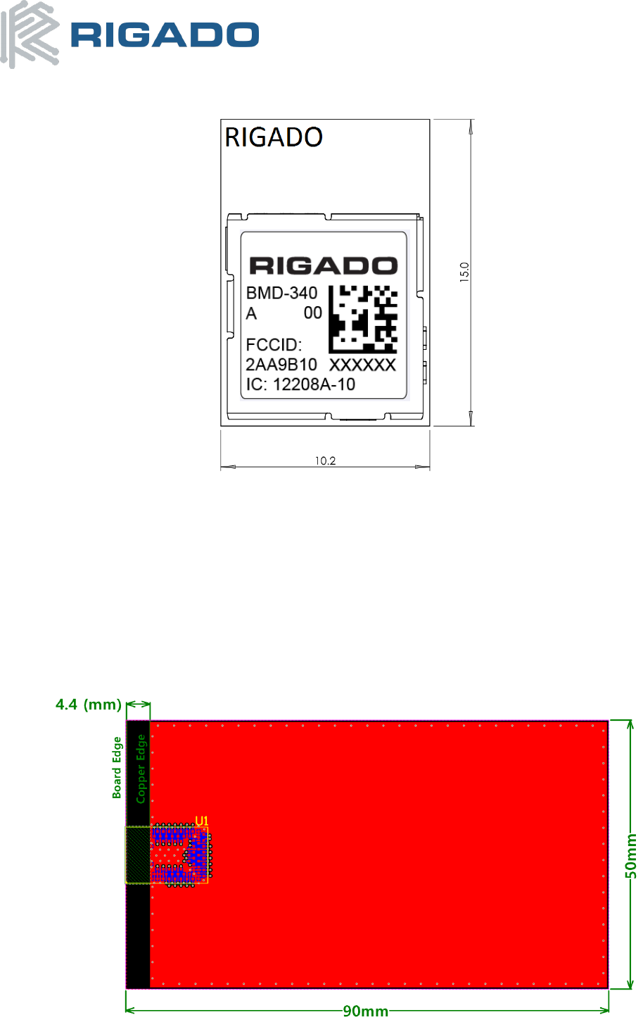
10. Module Marking
Figure 14 – BMD-340 Module Marking - Rev A
11. RF Design Notes
11.1 Recommended RF Layout & Ground Plane
The integrated antenna requires a suitable ground plane to radiate effectively.
The area under and extending out from the antenna portion of the module should be kept clear of copper and
other metal. The module should be placed at the edge of the PCB with the antenna edge facing out. Reducing
the ground plane from that shown in Figure 15 will reduce the effective radiated power.
Figure 15 – BMD-340 RF Example based on EVAL Board
BMD-340 Module Datasheet
Bluetooth 5 + 802.15.4
May 21, 2018
BMD-340-DS V1.0 Page 22 of 31
11.2 Mechanical Enclosure
Care should be taken when designing and placing the module into an enclosure. Metal should be kept clear
from the antenna area, both above and below. Any metal around the module can negatively impact RF
performance.
The module is designed and tuned for the antenna and RF components to be in free air. Any potting, epoxy fill,
plastic over-molding, or conformal coating can negatively impact RF performance and must be evaluated by
the customer.
11.3 Antenna Patterns
Antenna patterns are based on the BMD-340 Evaluation Kit with a ground plane size of 109mm x 56mm. X-Y-Z
orientation is shown in Figure 16:
Figure 16 – X-Y-Z Antenna Orientation
BMD-340 Module Datasheet
Bluetooth 5 + 802.15.4
May 21, 2018
BMD-340-DS V1.0 Page 23 of 31
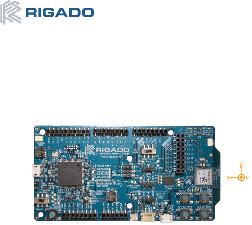
12. Evaluation Boards
Rigado has developed full featured evaluation boards that provide a complete I/O pin out to headers, on-
board programming and debug, 32.768 kHz crystal, power & virtual COM port over USB, BMD-340 USB
connector, 64Mb quad SPI Flash, 4 user LEDs, and 4 user buttons. The evaluation boards also provide the
option to be powered from a CR2032 coin cell battery or a LiPo battery through a JST-PH connecter, and have
current sense resistors and headers to allow for convenient current measurements. Arduino Mega style
headers are provided for easy prototyping of additional functions. The evaluation boards also support
programming off-board BMD-300/301 and BMD-340 Series modules.
Figure 17 – BMD-340 Evaluation Board
13. Edge Connectivity Solutions
Rigado offers secure and scalable device-to-cloud connectivity solutions with edge computing power that are
designed to perfectly interface with Rigado modules and streamline Commercial IoT deployments. The Rigado
Cascade platform provides IoT teams with secure edge computing, a containerized application platform and a
wide variety of wireless connectivity options – all in a simple ‘Edge-as-a-Service’ monthly subscription.
Visit www.rigado.com/iot-edge-as-a-service/ or contact Rigado at info@rigado.com for more details.

BMD-340 Module Datasheet
Bluetooth 5 + 802.15.4
May 21, 2018
BMD-340-DS V1.0 Page 24 of 31
14. Bluetooth Qualification
The BMD-340 Series modules will be qualified as a Bluetooth Component (tested) for RF-PHY. This allows
customers to use different SoftDevices that have been qualified by Nordic without the need to complete
additional RF-PHY testing. To achieve Bluetooth End Product qualification, the Rigado RF-PHY QDID can be
combined with Nordic QDIDs for the SoftDevice used when filing on the Bluetooth SIG website. The only
testing required is for the Bluetooth profiles supported by the customer’s product. Products with only custom
profiles do not require any additional testing.
• BMD-340: RF-PHY Component(Tested) Declaration ID TBD / QDID TBD
15. Regulatory Statements
15.1 FCC Statement:
This device has been tested and found to comply with part 15 of the FCC rules. These limits are designed to
provide reasonable protection against harmful interference in a residential installation. This equipment
generates, uses and can radiate radio frequency energy and, if not installed and used in accordance with the
instructions, may cause harmful interference to radio communications. However, there is no guarantee that
interference will not occur in a particular installation. If this equipment does cause harmful interference to
radio or television reception, which can be determined by turning the equipment off and on, the user is
encouraged to try to correct the interference by one or more of the following measures:
• Reorient or relocate the receiving antenna.
• Increase the separation between the equipment and the receiver
• Connect the equipment into an outlet on a circuit different from that to which the receiver is
connected.
• Consult the dealer or an experienced radio/TV technician for help.
Operation is subjected to the following two conditions: (1) This device may no cause harmful interference, and
(2) this device must accept any interference received, including interference that may cause undesired
operation. Note: Modification to this product will void the user’s authority to operate this equipment.
Note: Modification to this product will void the users’ authority to operate this equipment.
15.2 FCC Important Notes
(1) FCC Radiation Exposure Statement
This equipment complies with FCC RF radiation exposure limits set forth for an uncontrolled environment. This
transmitter must not be co-located or operating in conjunction with any other antenna or transmitter.
This equipment complies with Part 15 of the FCC Rules. Operation is subject the following two conditions:
(1) This device may not cause harmful interference, and
(2) This device must accept any interference received, including interference that may cause undesired
operation.
The devices must be installed and used in strict accordance with the manufacturer’s instructions as described
in this document.
Caution!
The manufacturer is not responsible for any radio or TV interference caused by unauthorized modifications to
this equipment. Such modification could void the user authority to operate the equipment.

BMD-340 Module Datasheet
Bluetooth 5 + 802.15.4
May 21, 2018
BMD-340-DS V1.0 Page 25 of 31
(2) Co-location Warning:
This device and its antenna(s) must not be co-located or operating in conjunction with any other transmitter
antenna.
(3) OEM integration instructions:
This device is intended only for OEM integrators under the following conditions:
The antenna and transmitter must not be co-located with any other transmitter or antenna. The module shall
be only used with the integral antenna(s) that has been originally tested and certified with this module.
As long as the two (2) conditions above are met, further transmitter testing will not be required. However, the
OEM integrator is still responsible for testing their end-product for any additional compliance requirements
with this module installed (for example, digital device emission, PC peripheral requirements, etc.)
In the event that these conditions cannot be met (for example certain laptop configuration or co-location with
another transmitter), then the FCC authorization for this module in combination with the host equipment is
no longer considered valid and the FCC ID of the module cannot be used on the final product. In these and
circumstance, the OEM integrator will be responsible for re-evaluating the end product (including the
transmitter) and obtaining a separate FCC authorization.
Caution!
The OEM is still responsible for verifying end product compliance with FCC Part 15, subpart B limits for
unintentional radiators through an accredited test facility.
The OEM integrator will be responsible to satisfy SAR/RF exposure requirements when the module
integrated into the host device.
(4) End product labeling:
The final end product must be labeled in a visible area with the following:
• BMD-340: “Contains FCC ID: 2AA9B10”
• Any similar wording that expresses the same meaning may be used.
The FCC Statement below should also be included on the label. When not possible, the FCC Statement should
be included in the User Manual of the host device.
“This device complies with part 15 of the FCC rules.
Operation is subject to the following two conditions. (1) This device may not cause harmful
interference. (2) This device must accept any interference received, including interference that may
cause undesired operation.”
(5) Information regarding the end user manual:
The OEM integrator has to be aware not to provide information to the end user regarding how to install or
remove this RF module in the user’s manual of the end product which integrates this module. The end user
manual shall include all required regulatory information/warning as show in this manual (Section 15.2(4)).

BMD-340 Module Datasheet
Bluetooth 5 + 802.15.4
May 21, 2018
BMD-340-DS V1.0 Page 26 of 31
15.3 IC Statement:
This device complies with Industry Canada license-exempt RSS standard(s). Operation is subject to the
following two conditions: (1) this device may not cause interference, and (2) this device must accept any
interference, including interference that may cause undesired operation of the device.
Le présent appareil est conforme aux CNR d'Industrie Canada applicables aux appareils radio exempts de
licence. L'exploitation est autorisée aux deux conditions suivantes : (1) l'appareil ne doit pas produire de
brouillage, et (2) l'utilisateur de l'appareil doit accepter tout brouillage radioélectrique subi, même si le
brouillage est susceptible d'en compromettre le fonctionnement.
RF exposure warning: The equipment complies with RF exposure limits set forth for an uncontrolled
environment. The antenna(s) used for this transmitter must not be co-located or operating in conjunction with
any other antenna or transmitter.
Avertissement d'exposition RF: L'équipement est conforme aux limites d'exposition aux RF établies pour un
incontrôlés environnement. L'antenne (s) utilisée pour ce transmetteur ne doit pas être co-localisés ou
onctionner en conjonction avec toute autre antenne ou transmetteur .
15.4 IC Important Notes
1. The OEM integrator must be aware not to provide information to the end user regarding how to install or
remove this RF module in the user manual of the end product.
The user manual which is provided by OEM integrators for end users must include the following information in
a prominent location.
L'intégrateur OEM doit être conscient de ne pas fournir d'informations à l'utilisateur final sur la manière
d'installer ou de retirer ce module RF dans le manuel d'utilisation du produit final.
Le manuel d'utilisation fourni par les intégrateurs OEM pour les utilisateurs finaux doit inclure les informations
suivantes dans un emplacement visible.
2. To comply with IC RF exposure compliance requirements, the antenna used for this transmitter must not be
co‐located or operating in conjunction with any other antenna or transmitter, except in accordance with IC
multi‐transmitter product procedures.
Pour se conformer aux exigences de conformité de l'exposition RF IC, l'antenne utilisée pour cet émetteur ne
doit pas être co-localisée ou fonctionner en conjonction avec une autre antenne ou un autre émetteur, sauf
conformément aux procédures du produit multi-émetteur IC.
3. The final system integrator must ensure there is no instruction provided in the user manual or customer
documentation indicating how to install or remove the transmitter module except such device has
implemented two‐ways authentication between module and the host system.
L'intégrateur système final doit s'assurer qu'aucune instruction n'est fournie dans le manuel de l'utilisateur ou
dans la documentation du client indiquant comment installer ou retirer le module transmetteur, sauf qu'un tel
dispositif a mis en place une authentification bidirectionnelle entre le module et le système hôte.
4. The host device shall be properly labelled to identify the module within the host device. The end product
must be labeled in a visible area with the following:
“Contains IC: 12208A-10 “
Any similar wording that expresses the same meaning may be used.

BMD-340 Module Datasheet
Bluetooth 5 + 802.15.4
May 21, 2018
BMD-340-DS V1.0 Page 27 of 31
Le périphérique hôte doit être correctement étiqueté pour identifier le module dans le périphérique hôte. Le
produit final doit être étiqueté dans une zone visible avec:
“Contains IC: 12208A-10 “
Toute formulation similaire exprimant la même signification peut être utilisée.
The IC Statement below should also be included on the label. When not possible, the IC Statement should be
included in the User Manual of the host device.
“This device complies with Industry Canada license-exempt RSS standard(s). Operation is subject to
the following two conditions: (1) this device may not cause interference, and (2) this device must
accept any interference, including interference that may cause undesired operation of the device.
Le présent appareil est conforme aux CNR d'Industrie Canada applicables aux appareils radio exempts
de licence. L'exploitation est autorisée aux deux conditions suivantes : (1) l'appareil ne doit pas
produire de brouillage, et (2) l'utilisateur de l'appareil doit accepter tout brouillage radioélectrique
subi, même si le brouillage est susceptible d'en compromettre le onctionnement.”
15.5 CE Regulatory
The BMD-340 module is being tested and is expected to be compliant against the following standards. OEM
integrators should consult with qualified test house to verify all regulatory requirements have been met for
their complete device.
EU - Radio Equipment Directive 2014/53/EU
• ETSI EN 300 328 V 2.1.1
• ETSI EN 301 489-1 V2.1.1
• ETSI EN 301 489-17 V3.1.1
Pending completion of testing, Declarations of Conformity and supporting test reports will be available at
www.rigado.com.
15.6 Australia / New Zealand
The BMD-340 module is to be tested to comply with the AS/NZS 4268 :2012+AMDT 1:2013, Radio equipment
and systems – Short range devices – Limits and methods of measurement. Pending test completion, the
report may be downloaded from www.rigado.com, and may be used as evidence in obtaining permission to
use the RCM.
Information on registration as a Responsible Party, license and labeling requirements may be found at the
following websites:
Australia: http://www.acma.gov.au/theACMA/radiocommunications-short-range-devices-standard-2004
New Zealand: http://www.rsm.govt.nz/compliance
The A-Tick and C-Tick marks are being migrated to the Regulatory Compliance Mark (RCM). Only Australian-
based and New Zealand-based companies who are registered may be granted permission to use the RCM. An
Australian-based or New Zealand-based agent or importer may also register as a Responsible Party to use the
RCM on behalf of a company not in Australia or New Zealand.
BMD-340 Module Datasheet
Bluetooth 5 + 802.15.4
May 21, 2018
BMD-340-DS V1.0 Page 28 of 31
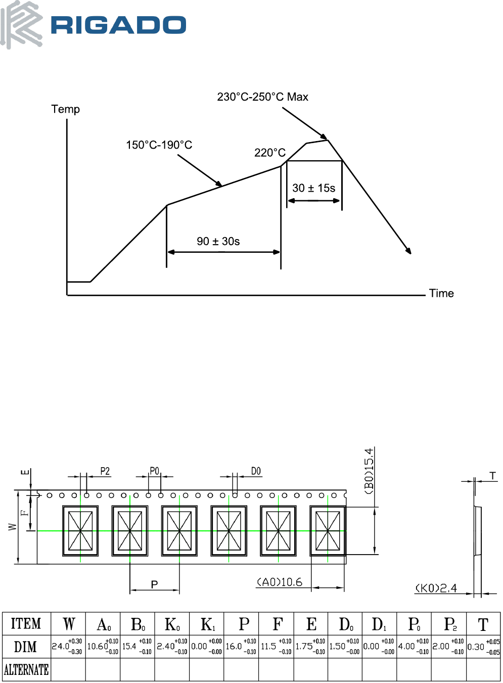
16. Solder Reflow Temperature-Time Profile
Figure 18 – Reflow Profile for Lead Free Solder
16.1 Moisture Sensitivity Level
The BMD-340 is rated for MSL 3, 168-hour floor life after opening.
17. Packaging and Labeling
17.1 Carrier Tape Dimensions
Figure 19 - BMD-340 Tape Dimensions
BMD-340 Module Datasheet
Bluetooth 5 + 802.15.4
May 21, 2018
BMD-340-DS V1.0 Page 29 of 31
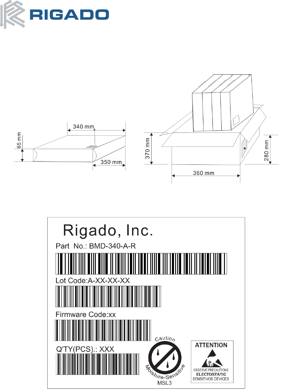
17.2 Reel Packaging
Modules come on 330mm reels loaded with 1000 modules. Each reel is placed in an antistatic bag with a
desiccant pack and humidity card and placed in a 340x350x65mm box. On the outside of the bag an antistatic
warning and reel label are adhered.
Figure 20 – Reel Packaging
17.3 Packaging Label
Figure 21 – Packaging Label

BMD-340 Module Datasheet
Bluetooth 5 + 802.15.4
May 21, 2018
BMD-340-DS V1.0 Page 30 of 31
18. Cautions
1) The guidelines of this document should be followed in order to assure proper performance of the module.
2) This product is for use in office, business, and residential applications, but not medical devices.
3) This module may short-circuit. If a short circuit can result in serious damage or injury then failsafe
precautions should be used. This could be accomplished by redundant systems and protection circuits.
4) Supply voltage to the module should not be higher than the specified inputs or reversed. Additionally, it
should not contain noise, spikes, or AC ripple voltage.
5) Avoid use with other high frequency circuits.
6) Use methods to eliminate static electricity when working with the module as it can damage the
components.
7) Contact with wires, the enclosure, or any other objects should be avoided.
8) Refer to the recommended pattern when designing for this module.
9) If hand soldering is used, be sure to use the precautions outlined in this document.
10) This module should be kept away from heat, both during storage and after installation.
11) Do not drop or physically shock the module.
12) Do not damage the interface surfaces of the module.
13) The module should not be mechanically stressed at any time (storage, handling, installation).
14) Do not store or expose this module to:
• Humid or salty air conditions
• High concentrations of corrosive gasses.
• Long durations of direct sunlight.
• Temperatures lower than -40°C or higher than 125°C.
19. Life Support Policy
This product is not designed to be used in a life support device or system, or in applications where there is potential
for a failure or malfunction to, directly or indirectly, cause significant injury. By using this product in an application
that poses these risks, such as described above, the customer is agreeing to indemnify Rigado for any damages that
result.

BMD-340 Module Datasheet
Bluetooth 5 + 802.15.4
May 21, 2018
BMD-340-DS V1.0 Page 31 of 31
20. Document History
Revision
Date
Changes / Notes
0.8
7/5/2017
Initial Release
1.0
5/21/2018
Production Release. Updated power specifications. Added details on REG0 related silicon
errata. Updated certification information. Added Zigbee information. Removed outdated
factory firmware information.
21. Related Documents
Rigado Documents:
• BMD-340 Product Brief
Nordic Documents:
Visit infocenter.nordicsemi.com for a comprehensive library of Nordic technical documentation.
• nRF52840 – nRF52840 Product Specification
• nRF52840 – nRF52840 Rev 1 Production Silicon Errata
• S140-SDS – nRF52840 S140 Soft Device Specification
• 802.15.4 – nRF5 SDK for Thread and Zigbee