u blox 11 BMD-345 Bluetooth 5 BLE + 802.15.4 module User Manual BMD 340 Datasheet
Rigado, Inc. BMD-345 Bluetooth 5 BLE + 802.15.4 module BMD 340 Datasheet
u blox >
Installation Manual

BMD-345-DS V1.0 Page 1 of 20
Rigado Inc.
3950 Fairview Industrial Dr.
Salem, Oregon 97302
866-6-RIGADO
modules@rigado.com
www.rigado.com/modules
BMD-345 Module for Bluetooth 5 and 802.15.4
The BMD-345 is an advanced, highly flexible, ultra-low power multiprotocol SoM that enables Bluetooth 5 (BLE) and
IEEE 802.15.4 (Thread and Zigbee) connectivity for portable, extremely low power embedded systems. With an ARM®
Cortex™-M4F CPU, integrated 2.4GHz transceiver, and an integrated antenna, the BMD-345 provides a complete RF
solution allowing faster time to market with reduced development costs. Providing full use of the Nordic nRF52840’s
capabilities and peripherals, the BMD-345 can power the most demanding applications, all while simplifying designs
and reducing BOM costs. The BMD-345 is an ideal solution for designs that require the latest Bluetooth 5 features or
802.15.4 based networking for Thread. Increased integration with built in USB and 5.5V compatible DC/DC supply
reduces design complexity and BOM cost, while expanding possible applications. BMD-345 designs are footprint
compatible with the BMD-301, providing low-cost flexibility for tiered product lineups.
1. Features
• Based on the Nordic nRF52840 SoC
• Bluetooth 5 Long Range, 2Mbs, and Advertising
Extension support
• Extended range with PA + LNA
• Support for host board antenna and u.FL
• IEEE 802.15.4 with Thread and Zigbee support
• No external components required
• ARM® Cortex™-M4F 32-bit processor
• ARM® TrustZone® Cryptocell 310 security
• True Random Number Generator
• Serial Wire Debug (SWD)
• Nordic SoftDevice ready
• 1MB embedded flash memory
• 256kB RAM
• 48 General Purpose I/O Pins
• -40C to +85 Temperature Range
• FCC: 2AA9B11
• 12-bit/200KSPS ADC
• One Full-Speed USB (12Mbps)
• Four SPI Master/Slave (8 Mbps)
• Quad SPI with Execute in Place (XIP)
• Low power comparator
• Temperature sensor
• Two 2-wire Master/Slave (I2C compatible)
• I2S audio interface
• Two UARTs (w/ CTS/RTS and DMA)
• 20 channel CPU independent Programmable
Peripheral Interconnect (PPI)
• Quadrature Demodulator (QDEC)
• 128-bit AES HW encryption
• 5 x 32bit, 3 x 24bit Real Timer Counters (RTC)
• NFC-A tag interface for OOB pairing
• Dimensions: 15.0 x 10.2 x 1.9mm
• IC: 12208A-11
BMD-345 Module Datasheet
Bluetooth 5 + 802.15.4
July 11, 2018
BMD-345-DS V1.0 Page 2 of 20
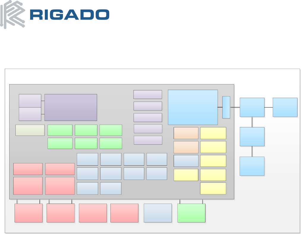
2. Block Diagram
BMD-345 Bluetooth 5 Low Energy SoC Module
32 MHz
Crystal
nRF52840-QIAA
1MB Flash
DC-DC
Inductor
Decoupling
Capacitors
Bulk
Capacitors
2.4GHz Radio
Multi-protocol
TWI
Master x2
SPI
Master x4
SPI Slave
x3
Core DC/DC
Buck Regulator
Core LDO
256kB
RAM
Low Power
Comparator
8-ch 12-bit
ADC
UART
x2 Quadrature
Decoder
SWD Debug &
Programming Temperature
Sensor
Cloc k
Management
Watchdog
Timer
Random Number
Gen
Timer x5
Accel Address
Resolver
AES CCM Mode
Encryption
AES ECB
Real Time
Counter x3
GPIO Task
Event Blocks
Programmable
Peripheral
Interconnect
ARM Cortex-M4F
@ 64MHz
PA / LNA +
RF Switch
Matching
Network
GPIO x48
(Analog x8)
I2S
TWI Slave
x2
PWM
x4 PDM
General
Purpose
Comparator
NFC Tag
Balun
DC-DC
Inductor
5V DC/DC Buck
Regulator TWI Slave
x2 QSPI Master
w/XIP USB2.0
5V LDO
ARM CryptoCell
SW
Interrupts
Memory
Watch Unit
u.FL
Connector
PCB Pad
Figure 1 – Block Diagram
BMD-345 V1.0 CONFIDENTIAL Page 3 of 20
Table of Contents
1. FEATURES ............................................................................................................................................................................... 1
2. BLOCK DIAGRAM .................................................................................................................................................................... 2
3. QUICK SPECIFICATIONS .......................................................................................................................................................... 5
4. PIN DESCRIPTIONS ................................................................................................................................................................. 6
4.1 BMD-345 ....................................................................................................................................................................................... 6
4.2 PERIPHERAL PINS ............................................................................................................................................................................... 8
4.2.1 BMD-301 to BMD-345 Pad Differences ...................................................................................................................................... 8
4.3 BMD-345 FANOUT EXAMPLE .................................................................................................................. ERROR! BOOKMARK NOT DEFINED.
5. ELECTRICAL SPECIFICATIONS .................................................................................................................................................. 9
5.1 ABSOLUTE MAXIMUM RATINGS............................................................................................................................................................. 9
5.2 OPERATING CONDITIONS ..................................................................................................................................................................... 9
5.3 POWER CONFIGURATION ................................................................................................................................................................... 10
5.3.1 USB Power ................................................................................................................................................................................ 10
5.4 GENERAL PURPOSE I/O ..................................................................................................................................................................... 10
5.5 MODULE RESET ............................................................................................................................................................................. 10
5.6 DEBUG & PROGRAMMING ................................................................................................................................................................. 10
5.7 CLOCKS .......................................................................................................................................................................................... 11
6. FIRMWARE ......................................................................................................................... ERROR! BOOKMARK NOT DEFINED.
6.1 FACTORY IMAGE .................................................................................................................................... ERROR! BOOKMARK NOT DEFINED.
6.2 SOFTDEVICES ........................................................................................................................................ ERROR! BOOKMARK NOT DEFINED.
6.2.1 S140 .............................................................................................................................................. Error! Bookmark not defined.
6.3 IEEE 802.15.4 (THREAD AND ZIGBEE) ...................................................................................................... ERROR! BOOKMARK NOT DEFINED.
6.4 MAC ADDRESS INFO ........................................................................................................................................................................ 12
7. MECHANICAL DATA ............................................................................................................ ERROR! BOOKMARK NOT DEFINED.
7.1 MECHANICAL DIMENSIONS ....................................................................................................................... ERROR! BOOKMARK NOT DEFINED.
7.2 RECOMMENDED PCB LAND PADS ........................................................................................................................................................ 13
8. MODULE MARKING ............................................................................................................ ERROR! BOOKMARK NOT DEFINED.
9. RF DESIGN NOTES ............................................................................................................... ERROR! BOOKMARK NOT DEFINED.
9.1 RECOMMENDED RF LAYOUT & GROUND PLANE ........................................................................................... ERROR! BOOKMARK NOT DEFINED.
9.2 ANTENNA PATTERNS ............................................................................................................................... ERROR! BOOKMARK NOT DEFINED.
10. BLUETOOTH QUALIFICATION ................................................................................................................................................ 13
11. REGULATORY STATEMENTS .................................................................................................................................................. 13
11.1 FCC STATEMENT: ............................................................................................................................................................................ 13
11.2 FCC IMPORTANT NOTES .................................................................................................................................................................... 14
11.3 IC STATEMENT: ............................................................................................................................................................................... 16
11.4 IC IMPORTANT NOTES ....................................................................................................................................................................... 16
11.5 CE REGULATORY .............................................................................................................................................................................. 17
11.6 AUSTRALIA / NEW ZEALAND ............................................................................................................................................................... 17
12. SOLDER REFLOW TEMPERATURE-TIME PROFILE ................................................................................................................... 18
12.1 MOISTURE SENSITIVITY LEVEL ............................................................................................................................................................. 18
13. PACKAGING AND LABELING .................................................................................................................................................. 18
13.1 CARRIER TAPE DIMENSIONS ................................................................................................................................................................ 18
13.2 REEL PACKAGING ............................................................................................................................................................................. 19
13.3 PACKAGING LABEL .................................................................................................................................. ERROR! BOOKMARK NOT DEFINED.
14. CAUTIONS ............................................................................................................................................................................ 19
15. LIFE SUPPORT POLICY ........................................................................................................................................................... 19
16. DOCUMENT HISTORY ........................................................................................................................................................... 20
List of Figures
FIGURE 1 – BLOCK DIAGRAM ................................................................................................................................................................. 2
FIGURE 2 – BMD-345 PIN OUT (TOP VIEW) ............................................................................................................................................ 6
FIGURE 6 – BMD-340 2 LAYER FANOUT EXAMPLE ...................................................................................... ERROR! BOOKMARK NOT DEFINED.
FIGURE 11 – BMD-345 MAC ADDRESS ON LABEL .................................................................................................................................. 12
FIGURE 12 – BMD-345 MODULE DIMENSIONS .......................................................................................... ERROR! BOOKMARK NOT DEFINED.
FIGURE 13 – BMD-345/301 DIMENSIONS (TOP VIEW)........................................................................................................................... 13
FIGURE 14 – BMD-345 MODULE MARKING .............................................................................................. ERROR! BOOKMARK NOT DEFINED.
FIGURE 15 – BMD-345 RF EXAMPLE BASED ON EVAL BOARD ...................................................................... ERROR! BOOKMARK NOT DEFINED.
FIGURE 16 – X-Y-Z ANTENNA ORIENTATION ............................................................................................... ERROR! BOOKMARK NOT DEFINED.
BMD-345 V1.0 CONFIDENTIAL Page 4 of 20
FIGURE 18 – REFLOW PROFILE FOR LEAD FREE SOLDER ............................................................................................................................. 18
FIGURE 19 - BMD-345 TAPE DIMENSIONS ............................................................................................................................................ 18
FIGURE 20 – REEL PACKAGING ............................................................................................................................................................. 19
FIGURE 21 – PACKAGING LABEL ................................................................................................................ ERROR! BOOKMARK NOT DEFINED.
List of Tables
TABLE 2 – QUICK SPECIFICATIONS ........................................................................................................................................................... 5
TABLE 3 – BMD-345 PIN DESCRIPTIONS ................................................................................................................................................. 7
TABLE 4 – PERIPHERAL PIN OPTIONS ....................................................................................................................................................... 8
TABLE 5 – PERIPHERALS WITH SHARED REGISTERS ...................................................................................................................................... 8
TABLE 6 – BMD-301 TO BMD-345 PAD DIFFERENCES ............................................................................................................................. 9
TABLE 7 – ABSOLUTE MAXIMUM RATINGS ............................................................................................................................................... 9
TABLE 8 – OPERATING CONDITIONS......................................................................................................................................................... 9
TABLE 10 – GPIO .............................................................................................................................................................................. 10
TABLE 11 – 32.768 KHZ CRYSTAL ........................................................................................................................................................ 11
TABLE 12 – 32.768 KHZ OSCILLATOR ................................................................................................................................................... 11

BMD-345 V1.0 CONFIDENTIAL Page 5 of 20
3. Quick Specifications
Bluetooth
Version
5.0 (Bluetooth Smart) Concurrent Central & Peripheral (S140)
Security
AES-128
LE connections
Up to 20 as Central, 1 as Peripheral, Observer, Broadcaster (S140)
IEEE 802.15.4
Thread Stack
OpenThread, Thread 1.1 certified
Thread Security
AES-128, ARM® Cryptocell accelerated
Zigbee Stack
Zigbee 3.0 (Certification Pending)
Radio
Frequency
2.402GHz to 2.480GHz
Modulations
GFSK at 1 Mbps and 2Mbps, QPSK at 250kbps
Transmit power
+15 dBm
Receiver sensitivity
-103dBm (2Mbps), -105 dBm (1Mbps), -113 (125ksps BLE), -110 dBm (IEEE 802.15.4)
Antenna
Integrated
Dimensions
BMD-345
Length
Width
Height
15.0 mm ± 0.3mm
10.2 mm ± 0.3mm
1.9 mm ± 0.1mm
Hardware
Interfaces
SPI Master/Slave x4
Quad SPI x1
UART x2
Two-Wire Master/Slave (I2C) x2
GPIO x48
I2S x1
PWM x12
PDM x1
USB 2.0 x1
Analog input x8
Power supply
VDD: 2.0V to 3.6V
VBUS: 4.35V to 5.5V (For USB operation)
Temperature Range
-40 to +85°C
Certifications
FCC
FCC part 15 modular certification
BMD-345 FCC ID: 2AA9B11
IC
Industry Canada RSS-210 modular certification
BMD-345 IC: 12208A-11
CE
EN 60950-1: 2011-01 3.1 (a): Health and Safety of the User
EN 301 489-1 V2.1.1& 3.1 (b): Electromagnetic Compatibility
EN 301 489-17 V3.1.1
EN 300 328 V2.1.1 3.2: Effective use of spectrum allocated
Australia / New Zealand
AS/NZS 4268 :2012+AMDT 1:2013, Radio equipment and systems – Short range devices
Bluetooth
BMD-345 RF-PHY Component (Tested) – DID: D040774; QDID: 114712
Table 1 – Quick Specifications
BMD-345 V1.0 CONFIDENTIAL Page 6 of 20
4. Pin Descriptions
4.1 BMD-345
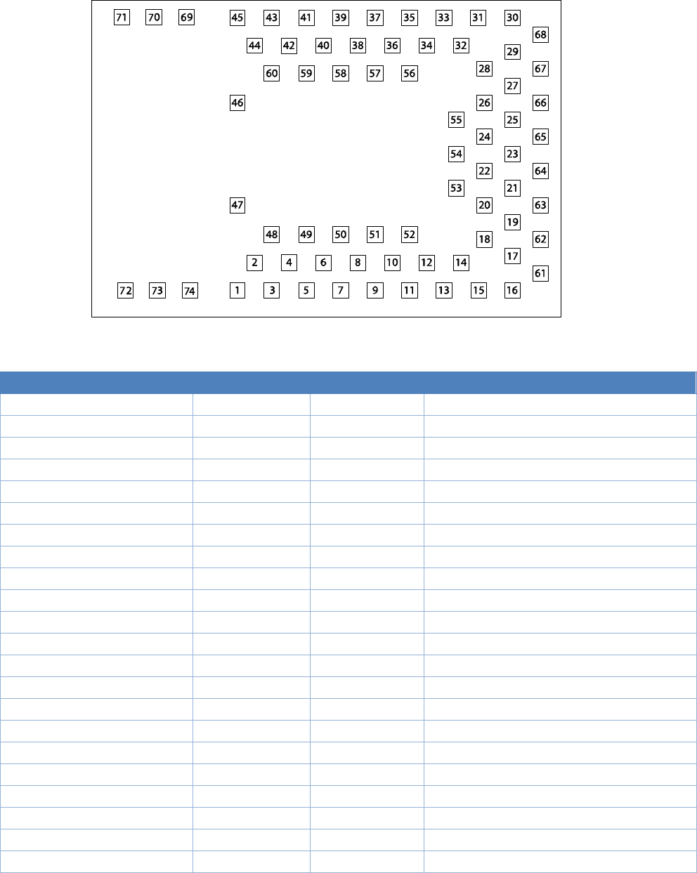
Figure 2 – BMD-345 Pin out (Top View)
Pin description
Pin
Name
Direction
Description
6
P0.25
In/Out
GPIO
7
P0.26
In/Out
GPIO
8
P0.27
In/Out
GPIO
9
P0.28
In/Out
GPIO/AIN42
10
P0.29
In/Out
GPIO/AIN52
11
P0.30
In/Out
GPIO/AIN62
12
P0.31
In/Out
GPIO/AIN72
13
P0.00
In/Out
GPIO/XTAL1 (32.768kHz)
14
P0.01
In/Out
GPIO/XTAL2 (32.768kHz)
15
P0.02
In/Out
GPIO/AIN02
19
P0.03
In/Out
GPIO/AIN12
20
P0.04
In/Out
GPIO/AIN2
21
P0.05
In/Out
GPIO/AIN3
22
P0.06
In/Out
GPIO
23
P0.07
In/Out
GPIO/TRACECLK
24
P0.08
In/Out
GPIO
25
P0.09
In/Out
GPIO/NFC12
26
P0.10
In/Out
GPIO/NFC22
27
P0.11
In/Out
GPIO/TRACEDATA[2]
28
P0.12
In/Out
GPIO/TRACEDATA[1]
31
P0.13
In/Out
GPIO
32
P0.14
In/Out
GPIO

BMD-345 V1.0 CONFIDENTIAL Page 7 of 20
Pin
Name
Direction
Description
33
P0.15
In/Out
GPIO
34
P0.16
In/Out
GPIO
35
P0.17
In/Out
GPIO
36
P0.21
In/Out
GPIO
37
P0.19
In/Out
GPIO
38
P0.20
In/Out
GPIO
39
P0.18
In/Out
GPIO/RESET
̅
̅
̅
̅
̅
̅
̅
̅
40
P0.22
In/Out
GPIO
41
P0.23
In/Out
GPIO
42
P0.24
In/Out
GPIO
43
SWCLK
In
SWD Clock
44
SWDIO
In/Out
SWD IO
48
P1.05
Out
PA_TX_EN
49
P1.06
Out
PA_RX_EN
50
P1.07
In/Out
GPIO2
51
P1.08
In/Out
GPIO
52
P1.09
In/Out
GPIO/TRACEDATA[3]
53
P1.10
In/Out
GPIO2
54
P1.11
In/Out
GPIO2
56
P1.00
In/Out
GPIO/TRACEDATA[0]/SWO
57
P1.01
In/Out
GPIO2
58
P1.02
Out
ANT_SEL
59
P1.03
In/Out
GPIO2
60
P1.04
Out
PA_MODE
61
P1.12
In/Out
GPIO2
62
P1.13
In/Out
GPIO2
63
P1.14
In/Out
GPIO2
64
P1.15
In/Out
GPIO2
67
USB-D-
In/Out
USB Data -
68
USB-D+
In/Out
USB Data +
66
VBUS
Power
USB PHY supply: 4.35V to 5.5V in
Connect to USB Host device 5V supply
17, 65
VCC1
Power In/Out
Connect to 2.0V to 3.6V DC supply
73
ANTA
RF Port
50Ω RF antenna port
1, 2, 3, 4, 5, 16, 18, 29, 30,
45, 46, 47, 55, 69, 70, 71,
72, 74
GND
Power
Electrical Ground
Note 1: An internal 4.7µF bulk capacitor is included on the module. However, it is good design practice to add additional bulk
capacitance as required for your application, i.e. those with heavy GPIO usage and/or current draw.
Note 2: These pins are in close proximity to the nRF52 radio power supply and antenna pins. Radio performance parameters, such
as sensitivity, may be affected by high frequency digital I/O with large sink/source current on these pins. Nordic recommends using
only low frequency, low-drive functions when possible.
Note 3: In HV mode, VCC acts as a regulated supply that can power other external devices. The voltage output of VCC can be
configured in software but is limited to no more than VCCH-0.3V. In System Off mode VCC can supply no more than 1mA.
Table 2 – BMD-345 Pin Descriptions

BMD-345 V1.0 CONFIDENTIAL Page 8 of 20
4.2 Peripheral Pins
The BMD-345 features a pin muxing system that allows most internal peripherals, such as UART and SPI, to be
used on any GPIO pin. This freedom in pin choice enables better optimization of designs and PCB layout. Note that
only one peripheral signal can be muxed to a GPIO pin at a time. Some functions are restricted to certain pins due
to additional internal circuitry required by the interface. These include: Trace signals, analog inputs, XTAL signals,
USB signals, SWD interface, and reset. See Table 3 below for details:
Peripheral
Signal
Pin Options
UART0, UART1
All
P0.00-P0.31, P1.00-P1.15
I2C0, I2C1
SPI0, SPI1, SPI2, SPI3
I2S0
QSPI0
PWM0, PWM1, PWM2, PWM3
PDN0
ADC, COMP, LPCOMP
All
P0.02-P0.05, P0.28-P0.31
(AIN0-AIN7)
NFC
NFC1
P0.09
NFC2
P0.10
Reset
RESET
̅
̅
̅
̅
̅
̅
̅
̅
P0.18
Trace
TRACECLK
P0.07
SWO/TRACEDATA[0]
P1.00
TRACEDATA[1]
P0.12
TRACEDATA[2]
P0.11
TRACEDATA[3]
P1.09
SWD
SWD Clock
SWCLK
SWD IO
SWDIO
32.768kHz Crystal
XTAL1
P0.00
XTAL2
P0.01
USB
USB Data +
USB-D+
USB Data -
USB-D-
Table 3 – Peripheral Pin Options
Note: Some peripherals on the BMD-345 share the same memory location for their registers. This means that only
one of these peripherals can be used at a time. It is possible to switch between peripherals that share the same
register location by clearing and reinitializing the associated configuration registers. See the Nordic Semiconductor
nRF52840 Product Specification for details.
Peripheral
ID
Base Address
Shared Peripherals
3
0x40003000
SPI0
I2C0
4
0x40004000
SPI1
I2C1
Table 4 – Peripherals with Shared Registers
4.2.1 BMD-301 to BMD-345 Pad Differences
Due to changes in the nRF52840 SoC used by the BMD-345, not all functions (such as SWO/TRACE signals) are
found on the same pins as on the BMD-301. Particularly of note is the reset pin function which on the BMD-345 is
now available on P0.18 instead of P0.21 as on the BMD-301. To maintain pin for pin compatibility of the reset

BMD-345 V1.0 CONFIDENTIAL Page 9 of 20
signal, P0.18 and P0.21 have swapped pad locations on the BMD-345 footprint. These differences are detailed in
Table 5 below:
Pin
BMD-301
Name
BMD-301
Function
BMD-345
Name
BMD-345
Function
39
P0.21
GPIO/RESET
̅
̅
̅
̅
̅
̅
̅
̅
P0.18
GPIO/RESET
̅
̅
̅
̅
̅
̅
̅
̅
38
P0.20
GPIO/TRACECLK
P0.20
GPIO
36
P0.18
GPIO/TRACEDATA[0]/SWO
P0.21
GPIO
34
P0.16
GPIO/TRACEDATA[1]
P0.16
GPIO
33
P0.15
GPIO/TRACEDATA[2]
P0.15
GPIO
32
P0.14
GPIO/TRACEDATA[3]
P0.14
GPIO
23
P0.07
GPIO
P0.07
GPIO/TRACECLK
56
N/A
N/A
P1.00
GPIO/TRACEDATA[0]/SWO
28
P0.12
GPIO
P0.12
GPIO/TRACEDATA[1]
27
P0.11
GPIO
P0.11
GPIO/TRACEDATA[2]
52
N/A
N/A
P1.09
GPIO/TRACEDATA[3]
Table 5 – BMD-301 to BMD-345 Pad Differences
5. Electrical Specifications
5.1 Absolute Maximum Ratings
Symbol
Parameter
Min.
Max.
Unit
VCC_MAX
Voltage on VCC supply pin
-0.3
3.9
V
VBUS_MAX
Voltage on VBUS Supply pin
-0.3
5.8
V
VIO_MAX
Voltage on GPIO pins (VCC > 3.6V)
-0.3
3.9
V
VIO_MAX
Voltage on GPIO pins (VCC ≤ 3.6V)
-0.3
VCC + 0.3V
V
TS
Storage Temperature Range
-40
125
°C
Table 6 – Absolute Maximum Ratings
5.2 Operating Conditions
Symbol
Parameter
Min.
Typ.
Max.
Unit
VCC_IN
VCC operating supply voltage in
2.0
3.0
3.6
V
VBUS_IN
VBUS operating supply voltage in
4.35
5.0
5.5
V
TR_VCC
VCC Supply rise time (0V to 2.0V)
-
-
60
ms
TA
Operating Ambient Temperature Range
-40
25
85
°C
Table 7 – Operating Conditions

BMD-345 V1.0 CONFIDENTIAL Page 10 of 20
5.3 Power Configuration
5.3.1 USB Power
The BMD-345 USB PHY is powered by a dedicated, internal LDO regulator that is fed by the VBUS pin (66). This
means that applying power to only the VBUS pin will not power the rest of the module. In order for the USB PHY
to operate, VBUS must be externally powered.
5.4 General Purpose I/O
The general purpose I/O is organized as two ports enabling access and control of the 48 available GPIO pins. The
first port allows access of P0.00 to P0.31, similar to the one port available on the BMD-301. The second port, new
to the BMD-345, allows access to P1.00 to P1.15. Each GPIO can be accessed individually with the following user
configurable features:
• Input/output direction
• Output drive strength
• Internal pull-up and pull-down resistors
• Wake-up from high or low level triggers on all pins
• Trigger interrupt on all pins
• All pins can be used by the PPI task/event system; the maximum number of pins that can be interfaced
through the PPI at the same time is limited by the number of GPIOTE channels
• All pins can be individually configured to carry serial interface or quadrature demodulator signals
Symbol
Parameter
Min.
Typ.
Max.
Unit
VIH
Input High Voltage
0.7 x VCC
-
VCC
V
VIL
Input Low Voltage
VSS
-
0.3 x VCC
V
VOH
Output High Voltage
VCC − 0.4
-
VCC
V
VOL
Output Low Voltage
VSS
-
VSS + 0.4
V
RPU
Pull-up Resistance
11
13
16
kΩ
RPD
Pull-down Resistance
11
13
16
kΩ
Table 8 – GPIO
5.5 Module RESET
GPIO pin P0.18 may be used for a hardware reset. In order to utilize P0.18 as a hardware reset, the UICR registers
PSELRESET[0] and PSELRESET[1] must be set alike, to the value of 0x7FFFFFD2. When P0.18 is programmed as
RESET
̅
̅
̅
̅
̅
̅
̅
̅
, the internal pull-up is automatically enabled. Rigado and Nordic example applications and development
kits program P0.18 as RESET
̅
̅
̅
̅
̅
̅
̅
̅
.
5.6 Debug & Programming
The BMD-345 supports the two pin Serial Wire Debug (SWD) interface and offers flexible and powerful
mechanisms for non-intrusive debugging of program code. Breakpoints, single stepping, and instruction trace
capture of code execution flow are part of this support.
The BMD-345 also supports ETM and ITM trace. Trace data from the ETM and the ITM is sent to an external
debugger via a 4-bit wide parallel trace port. In addition to parallel trace, the TPIU supports serial trace via the
Serial Wire Output (SWO) trace protocol.

BMD-345 V1.0 CONFIDENTIAL Page 11 of 20
5.7 Clocks
The BMD-345 requires two clocks, a high frequency clock and a low frequency clock.
The high frequency clock is provided on-module by a high-accuracy 32-MHz crystal as required by the
nRF52840 for radio operation.
The low frequency clock can be provided internally by an RC oscillator or synthesized from the fast clock; or
externally by a 32.768 kHz crystal. An external crystal provides the lowest power consumption and greatest
accuracy. Using the internal RC oscillator with calibration provides acceptable performance for BLE
applications at a reduced cost and slight increase in power consumption. Note: the ANT protocol requires the
use of an external crystal.
32.768 kHz Crystal (LFXO)
Symbol
Parameter
Typ.
Max.
Unit
FNOM_LFXO
Crystal frequency
32.768
-
kHz
FTOL_LFXO_BLE
Frequency tolerance, BLE applications
-
±250
ppm
CL_LFXO
Load Capacitance
-
12.5
pF
C0_LFXO
Shunt Capacitance
-
2
pF
RS_LFXO
Equivalent series resistance
-
100
kΩ
Cpin
Input Capacitance on XL1 & XL2 pads
4
-
pF
Table 9 – 32.768 kHz Crystal
32.768 kHz Oscillator Comparison
Symbol
Parameter
Min.
Typ.
Max.
Unit
ILFXO
Current for 32.768kHz Crystal Oscillator
-
0.23
-
µA
ILFRC
Current for 32.768kHz RC Oscillator
-
0.7
1
µA
ILFSYNT
Current for 32.768kHz Synthesized Oscillator
-
100
-
µA
fTOL_LFXO_BLE
Frequency Tolerance, 32.768kHz Crystal Oscillator
(BLE Stack)1
-
-
±250
ppm
fTOL_LFXO_ANT
Frequency Tolerance, 32.768kHz Crystal Oscillator
(ANT Stack)1
-
-
±50
ppm
f TOL_LFRC
Frequency Tolerance, 32.768kHz RC Oscillator
-
-
±2
%
fTOL_CAL_LFRC
Frequency tolerance, 32.768kHz RC after calibration
-
-
±250
ppm
fTOL_LFSYNT
Frequency Tolerance, 32.768kHz Synthesized
Oscillator
-
-
±48
ppm
Note 1: fTOL_LFXO_BLE and fTOL_LFXO_ANT are the max allowed for BLE and ANT applications. Actual tolerance depends
on the crystal used.
Table 10 – 32.768 kHz Oscillator
BMD-345 V1.0 CONFIDENTIAL Page 12 of 20
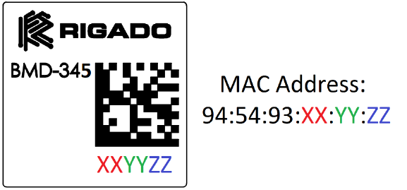
5.8 MAC Address Info
The BMD-345 modules comes preprogrammed with a unique MAC address from the factory. The MAC
address is also printed on a 2D barcode on the top of the module.
Figure 3 – BMD-345 MAC Address on Label
The 6-byte BLE Radio MAC address is stored in the nRF52840 UICR at NRF_UICR_BASE+0x80 LSB first. Please
read the MAC Address Provisioning application note if you are not using the built in bootloader to avoid
erasing/overwriting the MAC address during programming. Important: If full memory protection is enabled,
the UICR cannot be read via the SWD interface. If performing a full-erase, the MAC can then only be recovered
from the 2D barcode and human-readable text.
UICR Register:
NRF_UICR + 0x80 (0x10001080): MAC_Addr [0] (0xZZ)
NRF_UICR + 0x81 (0x10001081): MAC_Addr [1] (0xYY)
NRF_UICR + 0x82 (0x10001082): MAC_Addr [2] (0xXX)
NRF_UICR + 0x83 (0x10001083): MAC_Addr [3] (0x93)
NRF_UICR + 0x84 (0x10001084): MAC_Addr [4] (0x54)
NRF_UICR + 0x85 (0x10001085): MAC_Addr [5] (0x94)
BMD-345 V1.0 CONFIDENTIAL Page 13 of 20
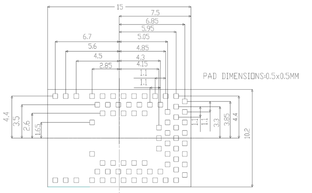
6. Recommended PCB Land Pads
Figure 4 – BMD-345 Dimension (Top View)
(All dimensions are in mm)
7. Bluetooth Qualification
The BMD-345 Series modules will be qualified as a Bluetooth Component (tested) for RF-PHY. This allows
customers to use different SoftDevices that have been qualified by Nordic without the need to complete
additional RF-PHY testing. To achieve Bluetooth End Product qualification, the Rigado RF-PHY QDID can be
combined with Nordic QDIDs for the SoftDevice used when filing on the Bluetooth SIG website. The only
testing required is for the Bluetooth profiles supported by the customer’s product. Products with only custom
profiles do not require any additional testing.
• BMD-345: RF-PHY Component(Tested) Declaration ID D040774/ QDID 114712
8. Regulatory Statements
8.1 FCC Statement:
This device has been tested and found to comply with part 15 of the FCC rules. These limits are designed to
provide reasonable protection against harmful interference in a residential installation. This equipment
generates, uses and can radiate radio frequency energy and, if not installed and used in accordance with the
instructions, may cause harmful interference to radio communications. However, there is no guarantee that
interference will not occur in a particular installation. If this equipment does cause harmful interference to
radio or television reception, which can be determined by turning the equipment off and on, the user is
encouraged to try to correct the interference by one or more of the following measures:
• Reorient or relocate the receiving antenna.
• Increase the separation between the equipment and the receiver
BMD-345 V1.0 CONFIDENTIAL Page 14 of 20
• Connect the equipment into an outlet on a circuit different from that to which the receiver is
connected.
• Consult the dealer or an experienced radio/TV technician for help.
Operation is subjected to the following two conditions: (1) This device may no cause harmful interference, and
(2) this device must accept any interference received, including interference that may cause undesired
operation. Note: Modification to this product will void the user’s authority to operate this equipment.
Note: Modification to this product will void the users’ authority to operate this equipment.
8.2 FCC Important Notes
(1) FCC Radiation Exposure Statement
This equipment complies with FCC RF radiation exposure limits set forth for an uncontrolled environment. This
transmitter should be installed and operated with a minimum distance of 20 centimeters between the
radiator and any human body and must not be co-located or operating in conjunction with any other antenna
or transmitter. This equipment complies with Part 15 of the FCC Rules. Operation is subject the following two
conditions:
(1) This device may not cause harmful interference, and
(2) This device must accept any interference received, including interference that may cause undesired
operation.
The devices must be installed and used in strict accordance with the manufacturer’s instructions as described
in this document.
Caution!
The manufacturer is not responsible for any radio or TV interference caused by unauthorized modifications to
this equipment. Such modification could void the user authority to operate the equipment.
(2) Co-location Warning:
This device and its antenna(s) must not be co-located or operating in conjunction with any other transmitter
antenna.
(3) OEM integration instructions:
This device is intended only for OEM integrators under the following conditions:
The antenna must be installed such that 20 cm is maintained between the antenna and users, and the
transmitter must not be co-located with any other transmitter or antenna. The module shall be only used with
the integral antenna(s) that has been originally tested and certified with this module.
As long as the two (2) conditions above are met, further transmitter testing will not be required. However, the
OEM integrator is still responsible for testing their end-product for any additional compliance requirements
with this module installed (for example, digital device emission, PC peripheral requirements, etc.)
In the event that these conditions cannot be met (for example certain laptop configuration or co-location with
another transmitter), then the FCC authorization for this module in combination with the host equipment is
no longer considered valid and the FCC ID of the module cannot be used on the final product. In these and
circumstance, the OEM integrator will be responsible for re-evaluating the end product (including the
transmitter) and obtaining a separate FCC authorization.
BMD-345 V1.0 CONFIDENTIAL Page 15 of 20
Caution!
The OEM is still responsible for verifying end product compliance with FCC Part 15, subpart B limits for
unintentional radiators through an accredited test facility.
(4) End product labeling:
The final end product must be labeled in a visible area with the following:
• BMD-345: “Contains FCC ID: 2AA9B11”
• Any similar wording that expresses the same meaning may be used.
The FCC Statement below should also be included on the label. When not possible, the FCC Statement should
be included in the User Manual of the host device.
“This device complies with part 15 of the FCC rules.
Operation is subject to the following two conditions. (1) This device may not cause harmful
interference. (2) This device must accept any interference received, including interference that may
cause undesired operation.”
(5) Information regarding the end user manual:
The OEM integrator has to be aware not to provide information to the end user regarding how to install or
remove this RF module in the user’s manual of the end product which integrates this module. The end user
manual shall include all required regulatory information/warning as show in this manual (Section 15.2(4)).
BMD-345 V1.0 CONFIDENTIAL Page 16 of 20
8.3 IC Statement:
This device complies with Industry Canada license-exempt RSS standard(s). Operation is subject to the
following two conditions: (1) this device may not cause interference, and (2) this device must accept any
interference, including interference that may cause undesired operation of the device.
Le présent appareil est conforme aux CNR d'Industrie Canada applicables aux appareils radio exempts de
licence. L'exploitation est autorisée aux deux conditions suivantes : (1) l'appareil ne doit pas produire de
brouillage, et (2) l'utilisateur de l'appareil doit accepter tout brouillage radioélectrique subi, même si le
brouillage est susceptible d'en compromettre le fonctionnement.
RF exposure warning: The equipment complies with RF exposure limits set forth for an uncontrolled
environment. The antenna(s) used for this transmitter must not be co-located or operating in conjunction with
any other antenna or transmitter.
Avertissement d'exposition RF: L'équipement est conforme aux limites d'exposition aux RF établies pour un
incontrôlés environnement. L'antenne (s) utilisée pour ce transmetteur ne doit pas être co-localisés ou
onctionner en conjonction avec toute autre antenne ou transmetteur .
8.4 IC Important Notes
1. The OEM integrator must be aware not to provide information to the end user regarding how to install or
remove this RF module in the user manual of the end product.
The user manual which is provided by OEM integrators for end users must include the following information in
a prominent location.
2. To comply with IC RF exposure compliance requirements, the antenna used for this transmitter must be
installed to provide a separation distance of at least 20 cm from all persons and must not be co‐located or
operating in conjunction with any other antenna or transmitter, except in accordance with IC multi‐
transmitter product procedures.
3. The final system integrator must ensure there is no instruction provided in the user manual or customer
documentation indicating how to install or remove the transmitter module except such device has
implemented two‐ways authentication between module and the host system.
4. The host device shall be properly labelled to identify the module within the host device. The end product
must be labeled in a visible area with the following:
• BMD-345: “Contains IC: 12208A-11“
Any similar wording that expresses the same meaning may be used.
The IC Statement below should also be included on the label. When not possible, the IC Statement should be
included in the User Manual of the host device.
“This device complies with Industry Canada license-exempt RSS standard(s). Operation is subject to
the following two conditions: (1) this device may not cause interference, and (2) this device must
accept any interference, including interference that may cause undesired operation of the device.
Le présent appareil est conforme aux CNR d'Industrie Canada applicables aux appareils radio exempts de
licence. L'exploitation est autorisée aux deux conditions suivantes : (1) l'appareil ne doit pas produire de
brouillage, et (2) l'utilisateur de l'appareil doit accepter tout brouillage radioélectrique subi, même si le
brouillage est susceptible d'en compromettre le onctionnement.”

BMD-345 V1.0 CONFIDENTIAL Page 17 of 20
8.5 CE Regulatory
The BMD-345 module is being tested and is expected to be compliant against the following standards. OEM
integrators should consult with qualified test house to verify all regulatory requirements have been met for
their complete device.
EU - Radio Equipment Directive 2014/53/EU
• ETSI EN 300 328 V 2.1.1
• ETSI EN 301 489-1 V2.1.1
• ETSI EN 301 489-17 V3.1.1
Pending completion of testing, Declarations of Conformity and supporting test reports will be available at
www.rigado.com.
8.6 Australia / New Zealand
The BMD-345 module is to be tested to comply with the AS/NZS 4268 :2012+AMDT 1:2013, Radio equipment
and systems – Short range devices – Limits and methods of measurement. Pending test completion, the
report may be downloaded from www.rigado.com, and may be used as evidence in obtaining permission to
use the RCM.
Information on registration as a Responsible Party, license and labeling requirements may be found at the
following websites:
Australia: http://www.acma.gov.au/theACMA/radiocommunications-short-range-devices-standard-2004
New Zealand: http://www.rsm.govt.nz/compliance
The A-Tick and C-Tick marks are being migrated to the Regulatory Compliance Mark (RCM). Only Australian-
based and New Zealand-based companies who are registered may be granted permission to use the RCM. An
Australian-based or New Zealand-based agent or importer may also register as a Responsible Party to use the
RCM on behalf of a company not in Australia or New Zealand.
BMD-345 V1.0 CONFIDENTIAL Page 18 of 20
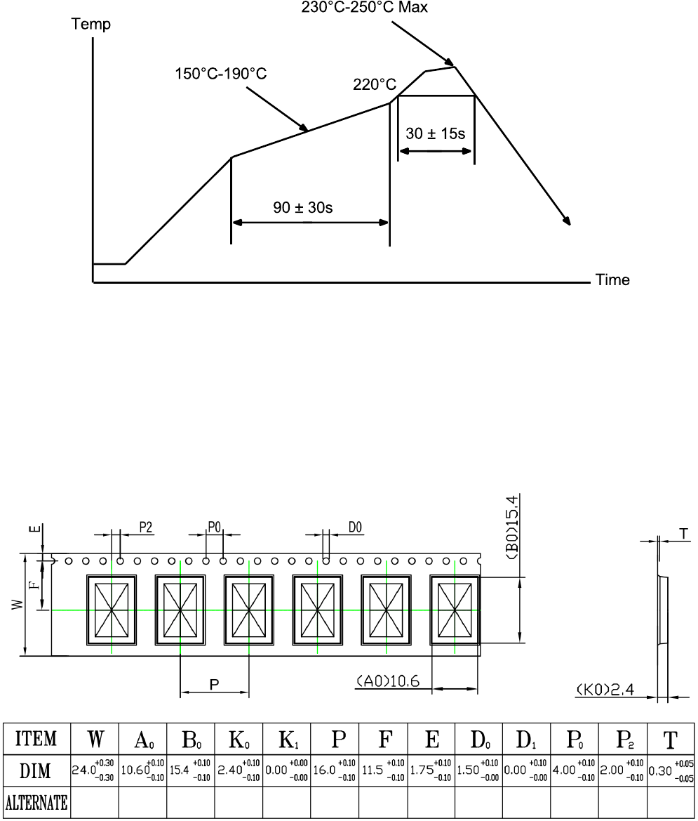
9. Solder Reflow Temperature-Time Profile
Figure 5 – Reflow Profile for Lead Free Solder
9.1 Moisture Sensitivity Level
The BMD-345 is rated for MSL 3, 168-hour floor life after opening.
10. Packaging and Labeling
10.1 Carrier Tape Dimensions
Figure 6 - BMD-345 Tape Dimensions
BMD-345 V1.0 CONFIDENTIAL Page 19 of 20
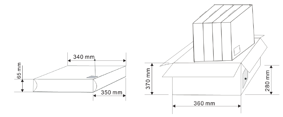
10.2 Reel Packaging
Modules come on 330mm reels loaded with 1000 modules. Each reel is placed in an antistatic bag with a
desiccant pack and humidity card and placed in a 340x350x65mm box. On the outside of the bag an antistatic
warning and reel label are adhered.
Figure 7 – Reel Packaging
11. Cautions
1) The guidelines of this document should be followed in order to assure proper performance of the module.
2) This product is for use in office, business, and residential applications, but not medical devices.
3) This module may short-circuit. If a short circuit can result in serious damage or injury then failsafe
precautions should be used. This could be accomplished by redundant systems and protection circuits.
4) Supply voltage to the module should not be higher than the specified inputs or reversed. Additionally, it
should not contain noise, spikes, or AC ripple voltage.
5) Avoid use with other high frequency circuits.
6) Use methods to eliminate static electricity when working with the module as it can damage the
components.
7) Contact with wires, the enclosure, or any other objects should be avoided.
8) Refer to the recommended pattern when designing for this module.
9) If hand soldering is used, be sure to use the precautions outlined in this document.
10) This module should be kept away from heat, both during storage and after installation.
11) Do not drop or physically shock the module.
12) Do not damage the interface surfaces of the module.
13) The module should not be mechanically stressed at any time (storage, handling, installation).
14) Do not store or expose this module to:
• Humid or salty air conditions
• High concentrations of corrosive gasses.
• Long durations of direct sunlight.
• Temperatures lower than -40°C or higher than 125°C.
12. Life Support Policy
This product is not designed to be used in a life support device or system, or in applications where there is potential
for a failure or malfunction to, directly or indirectly, cause significant injury. By using this product in an application
that poses these risks, such as described above, the customer is agreeing to indemnify Rigado for any damages that
result.

BMD-345 V1.0 CONFIDENTIAL Page 20 of 20
13. Document History
Revision
Date
Changes / Notes
1.0
7/11/2017
Initial Release