u blox JODYW164 WLAN/Bluetooth host-based multiradio module JODY-W1 User Manual JODY W1 series
u-blox AG WLAN/Bluetooth host-based multiradio module JODY-W1 JODY W1 series
u blox >
Contents
- 1. Data Sheet
- 2. Antenna Reference Design Guide
Data Sheet
![JODY-W1 series Host-based multiradio modules with Wi-Fi and Bluetooth Data Sheet Abstract This technical data sheet describes the JODY-W1 series modules with 2x2 MIMO 802.11n/ac and dual-mode Bluetooth® v4.2. JODY-W1 is ideal for in-vehicle-infotainment and telematics applications with simultaneous use cases requiring high data rates, such as in-car hotspots, Wi-Fi display applications such as Apple CarPlay, or video streaming across multiple clients. Connection to a host processor is through PCIe, SDIO, or High-Speed UART interfaces. www.u-blox.com UBX-16013635 - R10_draft](https://usermanual.wiki/u-blox/JODYW164.Data-Sheet/User-Guide-3927160-Page-1.png)
![JODY-W1 series - Data Sheet UBX-16013635 - R10_draft Confidential Page 2 of 50 Document Information Title JODY-W1 series Subtitle Host-based multiradio modules with Wi-Fi and Bluetooth Document type Data Sheet Document number UBX-16013635 Revision and date R10_draft 15-Jun-2018 Disclosure restriction Confidential Product Status Corresponding content status Functional Sample Draft For functional testing. Revised and supplementary data will be published later. In Development / Prototype Objective Specification Target values. Revised and supplementary data will be published later. Engineering Sample Advance Information Data based on early testing. Revised and supplementary data will be published later. Initial Production Early Prod. Information Data from product verification. Revised and supplementary data may be published later. Mass Production / End of Life Production Information Final product specification. This document applies to the following products: Product name Type number Chipset PCN reference Product Status JODY-W163-A JODY-W163-04A-00 CYW89359 N/A Engineering Sample JODY-W163-A JODY-W163-05A-00 CYW88359 N/A Engineering Sample JODY-W164-A JODY-W164-03A-01 CYW89359 N/A Engineering Sample JODY-W164-A JODY-W164-04A-00 CYW89359 N/A Engineering Sample JODY-W164-A JODY-W164-05A-00 CYW88359 N/A Engineering Sample JODY-W164-A JODY-W164-07A-01 CYW88359 N/A Engineering Sample JODY-W167-A JODY-W167-00A-00 CYW88359 N/A Engineering Sample JODY-W167-A JODY-W167-03A-00 CYW89359 N/A Engineering Sample JODY-W167 JODY-W167-00B-00 CYW88359 N/A Engineering Sample u-blox reserves all rights to this document and the information contained herein. Products, names, logos and designs described herein may in whole or in part be subject to intellectual property rights. Reproduction, use, modification or disclosure to third parties of this document or any part thereof without the express permission of u-blox is strictly prohibited. The information contained herein is provided “as is” and u-blox assumes no liability for the use of the information. No warranty, either express or implied, is given, including but not limited, with respect to the accuracy, correctness, reliability and fitness for a particular purpose of the information. This document may be revised by u-blox at any time. For most recent documents, visit www.u-blox.com. Copyright © 2018, u-blox AG. u-blox is a registered trademark of u-blox Holding AG in the EU and other countries.](https://usermanual.wiki/u-blox/JODYW164.Data-Sheet/User-Guide-3927160-Page-2.png)
![JODY-W1 series - Data Sheet UBX-16013635 - R10_draft Confidential Contents Page 3 of 50 Contents Contents .............................................................................................................................. 3 1 Functional description .................................................................................................. 6 1.1 Overview .............................................................................................................................................. 6 1.2 Applications .......................................................................................................................................... 6 1.3 Product features ................................................................................................................................... 7 1.4 Product description ............................................................................................................................... 7 1.5 Block diagrams ..................................................................................................................................... 7 1.6 Operation modes .................................................................................................................................. 9 1.6.1 Dual-band ..................................................................................................................................... 9 1.6.2 Single-band ................................................................................................................................. 10 1.7 Supported features ............................................................................................................................. 11 1.7.1 Wi-Fi Features.............................................................................................................................. 11 1.7.2 Bluetooth features ....................................................................................................................... 11 1.7.3 General product features ............................................................................................................. 11 1.7.4 Compliance ................................................................................................................................. 11 2 Interfaces .................................................................................................................... 12 2.1 Host interface configuration ............................................................................................................... 12 2.2 SDIO interface .................................................................................................................................... 12 2.2.1 Default speed and High speed modes ......................................................................................... 13 2.2.2 SDR12, SDR25, SDR50 Modes (up to 100 MHz) (1.8 V) ............................................................... 14 2.2.3 SDR104 Mode (208 MHz) (1.8 V) ................................................................................................ 15 2.2.4 DDR50 Mode (50 MHz) (1.8 V) .................................................................................................... 16 2.3 PCI Express interface ........................................................................................................................... 17 2.4 High Speed UART interface ................................................................................................................. 18 2.5 PCM Interface ..................................................................................................................................... 19 2.5.1 PCM Interface specifications ........................................................................................................ 20 2.6 I²S Interface ........................................................................................................................................ 24 2.6.1 I2S Interface specifications ............................................................................................................ 24 2.7 LTE Coexistence interface ................................................................................................................... 25 3 Pin definition .............................................................................................................. 26 3.1 Pin description .................................................................................................................................... 26 4 Electrical specification ................................................................................................ 29 4.1 Absolute maximum ratings ................................................................................................................. 29 4.2 Operating conditions .......................................................................................................................... 29 4.3 Digital pad ratings .............................................................................................................................. 29 4.4 Wi-Fi power consumption ................................................................................................................... 30 4.5 Bluetooth power consumption ........................................................................................................... 31 4.6 Radio specifications ............................................................................................................................ 31](https://usermanual.wiki/u-blox/JODYW164.Data-Sheet/User-Guide-3927160-Page-3.png)
![JODY-W1 series - Data Sheet UBX-16013635 - R10_draft Confidential Contents Page 4 of 50 4.6.1 Wi-Fi ........................................................................................................................................... 31 4.6.2 Bluetooth .................................................................................................................................... 32 5 Host drivers and firmware ......................................................................................... 33 5.1 General principle ................................................................................................................................ 33 5.2 Supported operating systems .............................................................................................................. 33 5.2.1 Linux ........................................................................................................................................... 33 6 Mechanical specifications .......................................................................................... 34 7 Approvals .................................................................................................................... 35 7.1 European Union regulatory compliance .............................................................................................. 35 7.2 FCC and IC compliance ...................................................................................................................... 35 7.2.1 FCC and ISED IDs ........................................................................................................................ 36 7.2.2 FCC compliance statement .......................................................................................................... 36 7.2.3 ISED compliance statement ......................................................................................................... 36 7.3 Certification in other countries ........................................................................................................... 38 7.4 Approved antennas ............................................................................................................................ 38 7.4.1 Wi-Fi operation............................................................................................................................ 38 7.4.2 Bluetooth operation .................................................................................................................... 38 7.5 Bluetooth qualification ....................................................................................................................... 39 7.5.1 Bluetooth host stack .................................................................................................................... 39 8 Product handling ........................................................................................................ 40 8.1 Packaging ........................................................................................................................................... 40 8.1.1 Reels ........................................................................................................................................... 40 8.1.2 Tapes .......................................................................................................................................... 40 8.2 Shipment, storage and handling ......................................................................................................... 40 8.2.1 Moisture sensitivity levels ............................................................................................................. 40 8.2.2 Mounting process and soldering recommendations ..................................................................... 41 8.2.3 ESD handling precautions ............................................................................................................ 42 9 Labeling and ordering information ........................................................................... 43 9.1 Product labeling .................................................................................................................................. 43 Table ...................................................................................................................................................... 44 9.2 Explanation of codes........................................................................................................................... 44 9.3 Ordering codes ................................................................................................................................... 44 Appendix .......................................................................................................................... 46 A Glossary ...................................................................................................................... 46 Related documents........................................................................................................... 48 Revision history ................................................................................................................ 49](https://usermanual.wiki/u-blox/JODYW164.Data-Sheet/User-Guide-3927160-Page-4.png)
![JODY-W1 series - Data Sheet UBX-16013635 - R10_draft Confidential Contents Page 5 of 50 Contact .............................................................................................................................. 50](https://usermanual.wiki/u-blox/JODYW164.Data-Sheet/User-Guide-3927160-Page-5.png)
![JODY-W1 series - Data Sheet UBX-16013635 - R10_draft Confidential Functional description Page 6 of 50 1 Functional description 1.1 Overview The JODY-W1 series is a compact module based on the Cypress CYW88359 and CYW89359 AEC-Q100 compliant chipsets. It enables Wi-Fi, Bluetooth®, and Bluetooth low energy communication, and is thus ideal for in-vehicle-infotainment and telematics applications with simultaneous use cases requiring high data rates, such as in-car hotspots, Wi-Fi display applications such as Apple CarPlay, or video streaming across multiple clients. The JODY-W1 modules can be operated in the following modes: Wi-Fi 2x2 MIMO 802.11n/ac in 2.4 GHz or 5 GHz Wi-Fi 1x1 802.11ac in 2.4 / 5 GHz real simultaneous dual band Dual-mode Bluetooth v4.2, including audio, can be operated fully simultaneous with both Wi-Fi modes The JODY-W1 undergoes extended automotive qualification according to ISO 16750-4 and is manufactured in line with ISO/TS 16949. Connection to a host processor is through PCIe, SDIO, or High-Speed UART interfaces. The radio type approvals for JODY-W1 is pending for many countries, and more certifications are planned. 1.2 Applications Automotive applications In-car Access Point for internet access Usage of applications such as Apple CarPlay, Miracast etc., in the car Rear-seat display Rapid sync-n-go applications and fast content download to the vehicle Hands-free equipment (Bluetooth) Industrial applications Manufacturing floor automation, wireless control terminals and point-to-point backhaul Machine control Medical in-hospital applications Security and surveillance Outdoor content distribution Robust wireless connectivity in a broad range of industrial applications](https://usermanual.wiki/u-blox/JODYW164.Data-Sheet/User-Guide-3927160-Page-6.png)
![JODY-W1 series - Data Sheet UBX-16013635 - R10_draft Confidential Functional description Page 7 of 50 1.3 Product features Table 1: Key features of JODY-W1 series 1.4 Product description Model Description JODY-W163-A Automotive grade module with 2 antenna pins, RSDB mode with a single antenna pin. Support for SDIO host interface only. JODY-W164-A Automotive grade module with 2 antenna pins, RSDB mode with a single antenna pin. Support for PCIe host interface, except JODY-W164-07A-01. JODY-W167-A Automotive grade module with 3 antenna pins, RSDB mode with two antenna pins JODY-W167 Professional grade module with 3 antenna pins, RSDB mode with two antenna pins Table 2: Description of the module variants JODY-W167-A is recommended for applications that need 802.11n 2x2 MIMO operation in the 2.4 GHz band. 1.5 Block diagrams The block diagrams of the JODY-W1 series are provided in this section.](https://usermanual.wiki/u-blox/JODYW164.Data-Sheet/User-Guide-3927160-Page-7.png)
![JODY-W1 series - Data Sheet UBX-16013635 - R10_draft Confidential Functional description Page 8 of 50 Figure 1: Block diagram of JODY-W163-A and JODY-W164-A See Table 3 for available configurations and the corresponding product type numbers of JODY-W163-A and JODY-W164-A. Product type Antenna configuration Band-pass filters ANT0 ANT1 BPF_1 BPF_2 JODY-W164-03A-01 5 GHz Wi-Fi and Bluetooth 2.4 and 5 GHz Wi-Fi (RSDB operation supported) Non-LTE coexistence Non-LTE coexistence JODY-W163-04A-00, JODY-W163-05A-00 JODY-W164-04A-00, JODY-W164-05A-00 Bluetooth 2.4 and 5 GHz Wi-Fi (RSDB operation supported) Non-LTE coexistence Non-LTE coexistence JODY-W164-07A-01 Bluetooth 2.4 and 5 GHz Wi-Fi (RSDB operation supported) LTE coexistence Non-LTE coexistence Table 3: Supported JODY-W164-A / JODY-W163-A configurations JODY-W163-A and JODY-W164-A differ only in the offered host interface (SDIO or PCIe). The host interface configuration is programmed at production time into the module.](https://usermanual.wiki/u-blox/JODYW164.Data-Sheet/User-Guide-3927160-Page-8.png)
![JODY-W1 series - Data Sheet UBX-16013635 - R10_draft Confidential Functional description Page 9 of 50 Figure 2: Block diagram of JODY-W167(-A) 1.6 Operation modes 1.6.1 Dual-band 5 GHz Wi-Fi (1x1 SISO) / 2.4 GHz Wi-Fi (1x1 SISO) RSDB (+ Bluetooth). See Table 4 for further information.](https://usermanual.wiki/u-blox/JODYW164.Data-Sheet/User-Guide-3927160-Page-9.png)
![JODY-W1 series - Data Sheet UBX-16013635 - R10_draft Confidential Functional description Page 10 of 50 2.4 GHz band 5 GHz band Supported host interfaces Notes AP AP PCIe, SDIO Any channel STA STA PCIe, SDIO Any channel P2P (GO) P2P (GO) PCIe, SDIO Any channel. Supported via single wpa supplicant. P2P (GC) P2P (GC) PCIe, SDIO Any channel. Supported via single wpa supplicant. AP STA PCIe, SDIO Any channel STA AP PCIe, SDIO Any channel AP P2P (GO) PCIe, SDIO Any channel P2P (GO) AP PCIe, SDIO Any channel AP P2P (GC) PCIe, SDIO Any channel P2P (GC) AP PCIe, SDIO Any channel P2P (GO) STA PCIe, SDIO Any channel STA P2P (GO) PCIe, SDIO Any channel P2P (GC) STA PCIe, SDIO Any channel STA P2P (GC) PCIe, SDIO Any channel AP+STA AP PCIe, SDIO Any channel. AP+STA on the same 2.4 GHz channel. AP AP+STA PCIe, SDIO Any channel. AP+STA on the same 5 GHz channel. AP+STA P2P (GO) PCIe, SDIO Any channel. AP+STA on the same 2.4 GHz channel. P2P (GO) AP+STA PCIe, SDIO Any channel. AP+STA on the same 5 GHz channel. AP P2P (GO) + STA PCIe, SDIO Any channel. P2P (GO) + STA on the same 5 GHz channel. P2P (GO) + STA AP PCIe, SDIO Any channel. P2P (GO) + STA on the same 2.4 GHz channel. P2P (GO) P2P (GO) + STA PCIe, SDIO Any channel. P2P (GO) + STA on the same 5 GHz channel. P2P (GO) + STA P2P (GO) PCIe, SDIO Any channel. P2P (GO) + STA on the same 2.4 GHz channel. Table 4: Supported RSDB configurations 1.6.2 Single-band 5 GHz Wi-Fi (2x2 MIMO on JODY-W167(-A) and JODY-W164-03A-01) JODY-W163-A / JODY-W164-A: 2.4 GHz Wi-Fi (1x1 SISO) (+ Bluetooth) JODY-W167 / JODY-W167-A: 2.4 GHz Wi-Fi (2x2 MIMO) (+ Bluetooth) Wi-Fi operation as AP, STA, P2P (GO), and P2P (GC) is supported on any 2.4 GHz or 5 GHz channel. Configuration of simultaneous operation of AP+STA, P2P (GO)+STA and P2P (GC)+STA is also supported on the same 2.4 or 5 GHz channel. These configurations are independent of the used host interface (PCIe or SDIO).](https://usermanual.wiki/u-blox/JODYW164.Data-Sheet/User-Guide-3927160-Page-10.png)
![JODY-W1 series - Data Sheet UBX-16013635 - R10_draft Confidential Functional description Page 11 of 50 1.7 Supported features 1.7.1 Wi-Fi Features Wi-Fi standards: o IEEE 802.11a/b/g/n/ac/e/i/v/w/h2 in station and access point modes o IEEE 802.11d/u in station mode only Simultaneous client and access point operation (up to 10 clients supported in total) Supports Wi-Fi direct/P2P mode IEEE 802.11ac 2x2 antenna configuration IEEE 802.11 PHY data rates up to 866 Mbps WPA/WPA2 and WAPI STA encryption is supported by hardware WPA/WPA2 Enterprise 802.1X Wi-Fi channels: o 2.4 GHz: 1-13 o 5 GHz: 36-165 RSDB mode SU-MIMO configurations SDIO 3.0 host interface for Wi-Fi3 PCIe 3.0 at Gen1 speed host interface for Wi-Fi MWS/LTE coexistence serial transport interface for connecting an external and co-located LTE device 1.7.2 Bluetooth features Bluetooth v4.2 with Bluetooth Low Energy and Classic Bluetooth v2.1+EDR over high-speed UART interface PCM / I2S interface for voice applications MWS/LTE coexistence serial transport interface for connecting an external and co-located LTE device 1.7.3 General product features Driver support for Linux 3.x/4.x Low-power and sleep modes for Bluetooth and Wi-Fi core Coexistence arbitration for Wi-Fi/Bluetooth/LE/LTE operation Small footprint (19.8 mm x 13.8 mm), LGA package Automotive qualification tests (climatic, mechanical, and operating life tests) according ISO 16750-4 planned 1.7.4 Compliance RoHS compliant Radio type approvals for Europe, USA, Canada, Japan, Korea, and Taiwan4 2 The DFS master mode supported in non-RSDB firmware only. 3 The SDIO interface is supported only in Automotive grade. 4 Approvals are pending.](https://usermanual.wiki/u-blox/JODYW164.Data-Sheet/User-Guide-3927160-Page-11.png)
![JODY-W1 series - Data Sheet UBX-16013635 - R10_draft Confidential Interfaces Page 12 of 50 2 Interfaces 2.1 Host interface configuration JODY-W1 series module uses the Pin 6, Pin 7, and Pin 8 pins as host interface configuration input to set the desired operation mode following a reset. When you need to configure the pins for a certain module operation mode, you need to provide a 10 kΩ or less pull down resistor to the ground. No external circuitry is required to set a configuration pin to high logical level. External reset is not needed for proper operation due to internal power-up reset logic though it can be used by the host controller through the WL_EN / BT_EN (active high) in case of an abnormal module behavior. Depending on the module variant, either SDIO or PCIe Wi-Fi host interface must be used: PCIe enable Pin 6 SDIO disable Pin 7 SDIO VDD select Pin 8 VIO_SD supply Pin 4 Wi-Fi interface 1 1 1 3.3 V or 1.8 V PCIe 0 0 1 1.8 V SDIO 1.8 V 0 0 0 3.3 V SDIO 3.3 V Table 5: Module configuration JODY-W1 series modules are programmed at factory to support either SDIO or PCIe host interface. The following sections specify the electrical characteristics of the two host interfaces. Refer to Table 6 for an overview of the supported host interface by product type. Product Name Order Number Host interface JODY-W163-A JODY-W163-04A SDIO JODY-W163-A JODY-W163-05A SDIO JODY-W164-A JODY-W164-03A PCIe JODY-W164-A JODY-W164-04A PCIe JODY-W164-A JODY-W164-05A PCIe JODY-W164-A JODY-W164-07A SDIO JODY-W167-A JODY-W167-00A PCIe JODY-W167-A JODY-W167-03A PCIe JODY-W167 JODY-W167-00B PCIe Table 6: Supported host interfaces per product 2.2 SDIO interface The SDIO device interface conforms to the industry standard SDIO 3.0 specification (UHS-I, up to 104 MByte/s) and allows a host controller using the SDIO bus protocol to access the Wi-Fi functions of the JODY-W1 series modules. The interface supports 4-bit SDIO transfer mode at the full clock range of 0 to 208 MHz.](https://usermanual.wiki/u-blox/JODYW164.Data-Sheet/User-Guide-3927160-Page-12.png)
![JODY-W1 series - Data Sheet UBX-16013635 - R10_draft Confidential Interfaces Page 13 of 50 2.2.1 Default speed and High speed modes Figure 3: SDIO Protocol timing diagram- Default speed mode (3.3 V) Figure 4: SDIO Protocol timing diagram – High speed mode (3.3 V) SDIO_CLKINPUTOUTPUTfPPtTHLtWLtWHtTLHtODLY(max)tODLY(min)tISUtIHSDIO_CLKINPUTOUTPUTfPPtTHLtWLtWHtTLHtODLYtOHtISUtIH50% VCC](https://usermanual.wiki/u-blox/JODYW164.Data-Sheet/User-Guide-3927160-Page-13.png)
![JODY-W1 series - Data Sheet UBX-16013635 - R10_draft Confidential Interfaces Page 14 of 50 Symbol Parameter Condition Min. Typ Max. Units fPP Clock frequency – Data Transfer Mode Normal 0 - 25 MHz High speed 0 - 50 MHz fOD Clock frequency – Identification Mode Normal 0 400 kHz High speed 0 - 400 kHz tWL Clock low time Normal 10 - - ns High speed 7 - - ns tWH Clock high time Normal 10 - - ns High speed 7 - - ns tTLH Clock rise time Normal - - 10 ns High speed - - 3 ns tTHL Clock low time Normal - - 10 ns High speed - - 3 ns tISU Input setup time Normal 5 - - ns High speed 6 - - ns tIH Input hold time Normal 5 - - ns High speed 2 - - ns tODLY Output delay time – Data Transfer Mode Normal 0 - 14 ns High speed - - 14 ns tODLY Identification Mode Normal 0 - 50 ns tODLY Output delay time CL ≤ 40 pF (1 card) Normal 0 - 14 ns tOH Output hold time High speed 2.5 - - ns CL Total system capacitance (each line) High speed 0 - 40 pF Table 7: SDIO Timing data – Default speed, High speed modes (3.3 V) 2.2.2 SDR12, SDR25, SDR50 Modes (up to 100 MHz) (1.8 V) Figure 5: SDIO Protocol timing diagram – SDR12, SDR25, SDR50 modes (up to 100 MHz) (1.8 V) SDIO_CLKINPUTOUTPUT fPPtCFtCRtODLYtOHtIStIH50% VCCTCLK](https://usermanual.wiki/u-blox/JODYW164.Data-Sheet/User-Guide-3927160-Page-14.png)
![JODY-W1 series - Data Sheet UBX-16013635 - R10_draft Confidential Interfaces Page 15 of 50 Symbol Parameter Condition Min. Typ Max. Units fPP Clock frequency SDR12 0 - 25 MHz SDR25 0 - 50 MHz SDR50 0 - 100 MHz tIS Input setup time SDR12/25/50 3 - - ns tIH Input hold time SDR12/25/50 0.8 - - ns tCLK Clock time SDR12/25/50 10 - 40 ns - Clock duty SDR12/25/50 30 70 % tCR, tCF, Rise time, fall time TCR, TCF < 2 ns (max) at 100 MHz CCARD = 10 pF SDR12/25/50 - 0.2*TCLK ns tODLY Output delay time CL ≤ 30 pF SDR12/25 - - 14 ns SDR50 - 7.5 tOH Output hold time CL = 15 pF SDR12/25/50 1.5 - - ns Table 8: SDIO Timing data – SDR12, SDR25, SDR50 modes (up to 100 MHz) (1.8 V) 2.2.3 SDR104 Mode (208 MHz) (1.8 V) Figure 6: SDIO Protocol timing diagram – SDR104 mode (208 MHz) Symbol Parameter Condition Min. Typ Max. Units fPP Clock frequency SDR104 0 - 208 MHz TIS Input setup time SDR104 1.4 - - ns TIH Input hold time SDR104 0.8 - - ns TCLK Clock time SDR104 4.8 - - ns tCR, tCF, Rise time, fall time TCR, TCF < 0.96 ns (max) at 208 MHz CCARD = 10 pF SDR104 - 0.2*TCLK ns TOP Card output phase SDR104 0 - 2 UI dTOP Delay variation due to temperature change after tuning SDR104 -350 +1550 ps TODW Output timing of variable data window SDR104 0.6 - - UI Table 9: SDIO Timing data – SDR104 mode (208 MHz) SDIO_CLKINPUTOUTPUT fPPtCFtCRtOPtODWtIStIH50% VCCTCLK](https://usermanual.wiki/u-blox/JODYW164.Data-Sheet/User-Guide-3927160-Page-15.png)
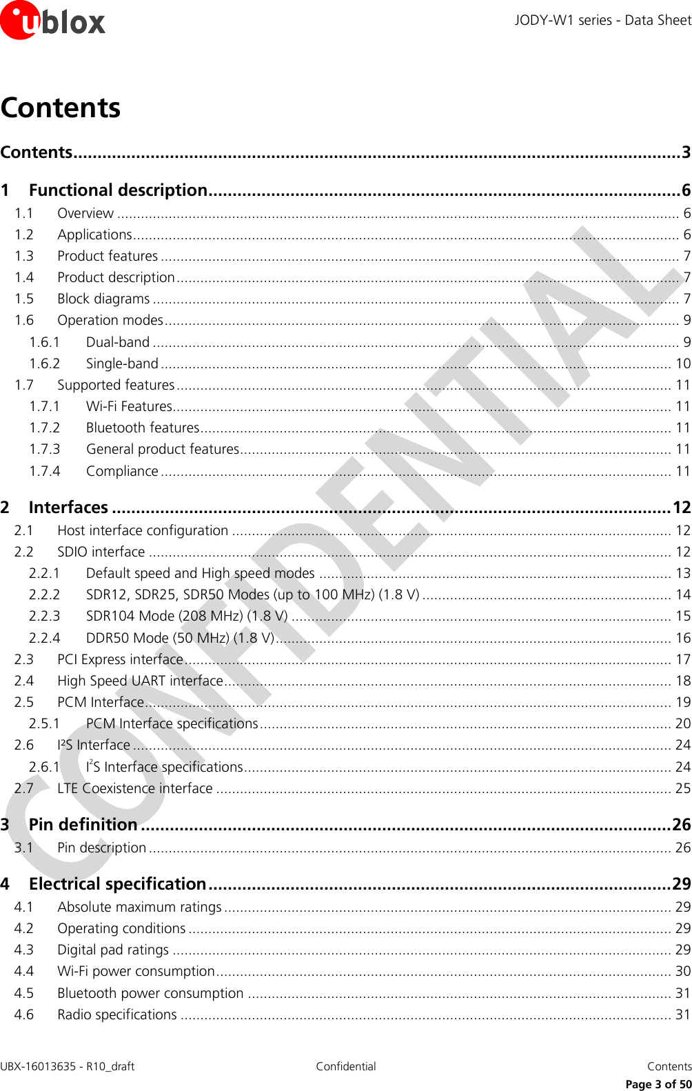
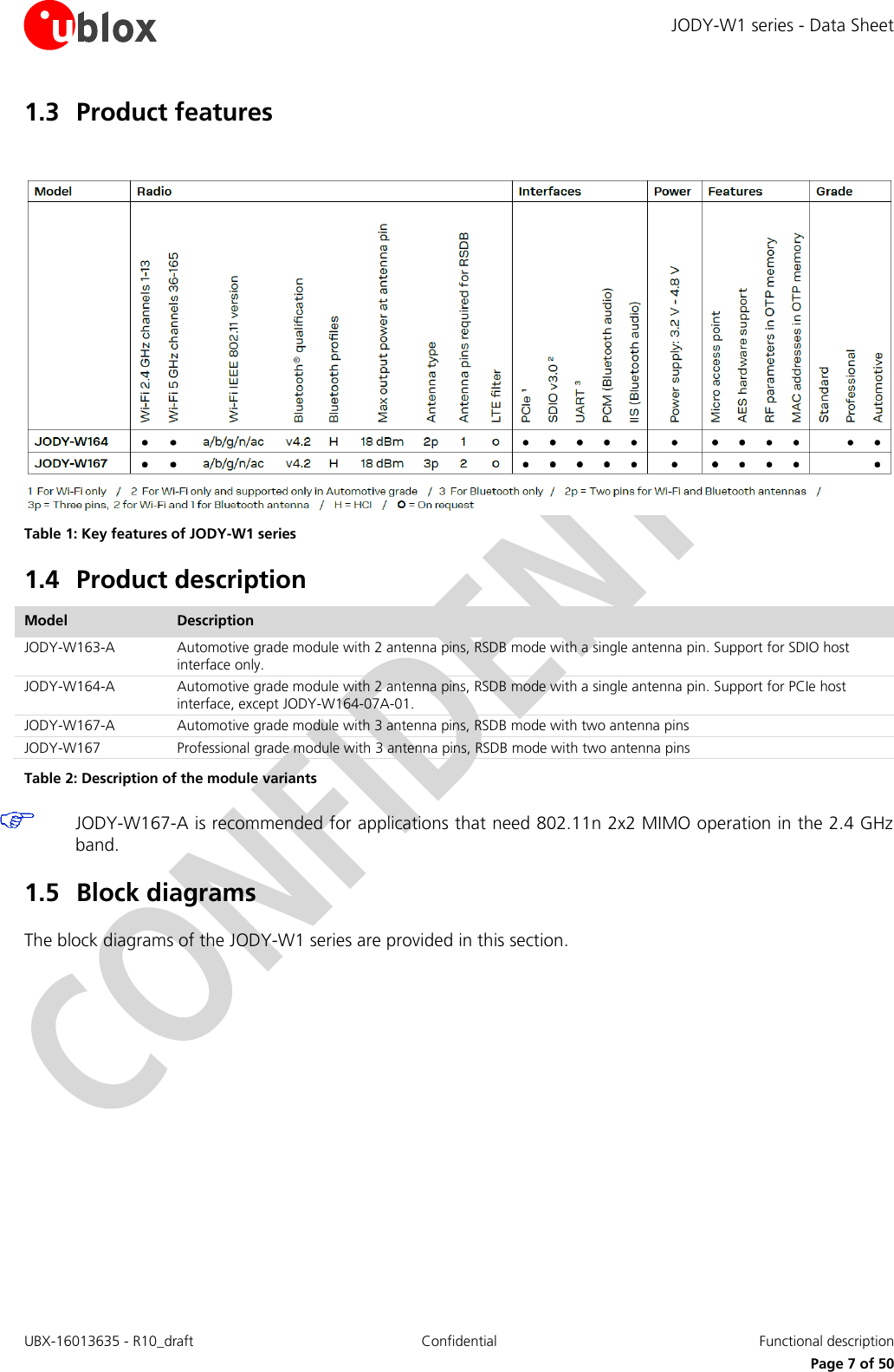
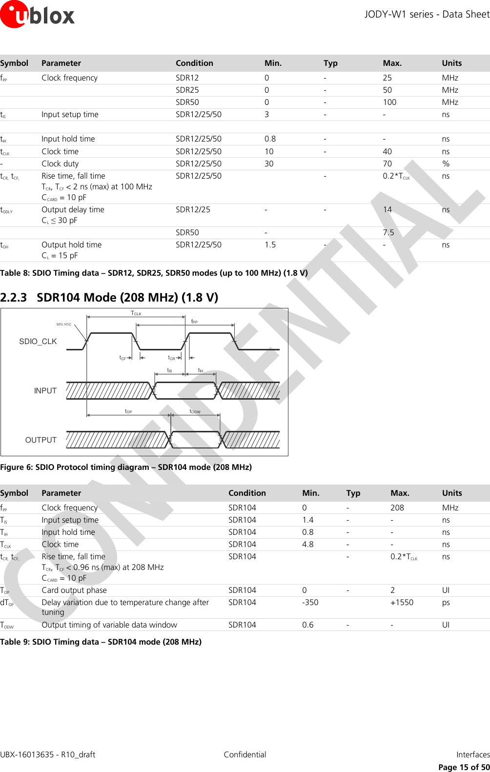
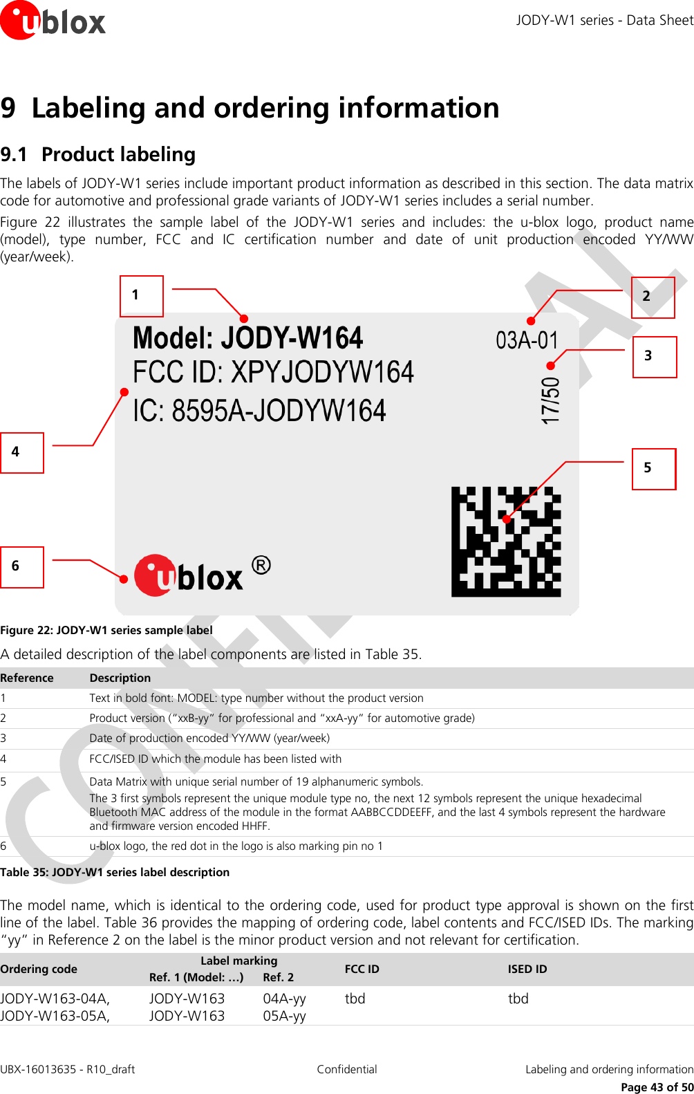
![JODY-W1 series - Data Sheet UBX-16013635 - R10_draft Confidential Interfaces Page 16 of 50 2.2.4 DDR50 Mode (50 MHz) (1.8 V) Figure 7: SDIO CMD Timing diagram – DDR50 mode (50 MHz) Figure 8: SDIO DAT[3:0] Timing diagram – DDR50 mode (50 MHz) Symbol Parameter Condition Min. Typ Max. Units Clock TCLK Clock time 50 MHz (max) between rising edges DDR50 20 - - ns tCR, tCF, Rise time, fall time TCR, TCF < 4.00 ns (max) at 50 MHz CCARD = 10 pF DDR50 - - 0.2*TCLK ns Clock Duty DDR50 45 - 55 % CMD Input (referenced to clock rising edge) tIS Input setup time CCARD ≤ 10 pF (1 card) DDR50 6 - - ns tIH Input hold time CCARD ≤ 10 pF (1 card) DDR50 0.8 - - ns CMD Output (referenced to clock rising edge) tODLY Output delay time during data transfer mode CL ≤ 30 pF (1 card) DDR50 - - 13.7 ns tOHLD Output hold time CL ≥ 15 pF (1 card) DDR50 1.5 - - ns DAT[3:0] Input (referenced to clock rising and falling edges) tIS2x Input setup time CCARD ≤ 10 pF (1 card) DDR50 3 ns tIH2x Input hold time CCARD ≤ 10 pF (1 card) DDR50 0.8 ns SDIO_CLKCMD INPUTCMD OUTPUT fPPtCFtCRtODLYtOHLDtIStIH50% VCCTCLKSDIO_CLKDAT INPUTfPPtCFtCRtISU2x50% VCCTCLKDAT OUTPUTtIH2xtISU2xtIH2xtODLY2x(min)tODLY2x(max)tODLY2x(min)tODLY2x(max)](https://usermanual.wiki/u-blox/JODYW164.Data-Sheet/User-Guide-3927160-Page-16.png)
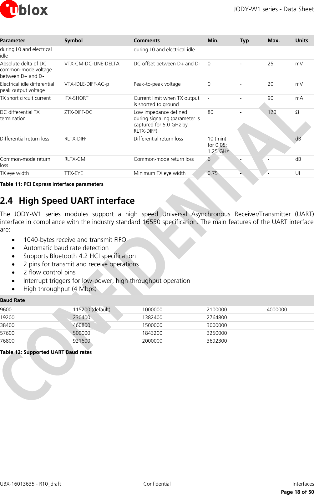
![JODY-W1 series - Data Sheet UBX-16013635 - R10_draft Confidential Interfaces Page 17 of 50 Symbol Parameter Condition Min. Typ Max. Units DAT[3:0] Output (referenced to clock rising and falling edges) tODLY2x (max) Output delay time during data transfer mode CL ≤ 25 pF (1 card) DDR50 7.5 ns tODLY2x (min) Output hold time CL ≥ 15 pF (1 card) DDR50 1.5 ns Table 10: SDIO Timing data – DDR50 mode (50 MHz) 2.3 PCI Express interface The PCI Express interface complies with the PCIe v3.0 standard at Gen1 speed and allows a host controller using the PCIe bus protocol to access the Wi-Fi function of the JODY-W1 series modules. The following table shows the parameters for the PCI Express interface. Parameter Symbol Comments Min. Typ Max. Units General Baud rate BPS - - 5 - Gbaud Reference clock amplitude Vref LVPECL, AC coupled 1 - - V Receiver Differential termination ZRX-DIFF-DC Differential termination 80 100 120 Ω DC impedance ZRX-DC DC common-mode impedance 40 50 60 Ω Power down termination (POS) ZRX-HIGH-IMP-DC-POS Power-down or RESET high impedance 100k - - Ω Power down termination (NEG) ZRX-HIGH-IMP-DC-NEG Power-down or RESET high impedance 1k - - Ω Input voltage VRX-DIFFp-p AC coupled, differential p-p 175 - - mV Jitter tolerance TRX-EYE Minimum receiver eye width 0.4 - - UI Differential return loss RLRX-DIFF Differential return loss 10 - - dB Common-mode return loss RLRX-CM Common-mode return loss 6 - - dB Unexpected electrical idle enter detect threshold integration time TRX-IDEL-DET-DIFF-ENTERTIME An unexpected electrical idle must be recognized no longer than this time to signal an unexpected idle condition - - 10 ms Signal detect threshold VRX-IDLE-DET-DIFFp-p Electrical idle detect threshold 65 - 175 mV Transmitter Output voltage VTX-DIFFp-p Differential p-p, programmable in 16 steps 0.8 - 1200 mV Output voltage rise time VTX-RISE 20% to 80% 0.125 (2.5 GT/s) 0.15 (5 GT/s) - - - - UI Output voltage fall time VTX-FALL 80% to 20% 0.125 (2.5 GT/s) 0.15 (5 GT/s) - - - - UI RX detection voltage swing VTX-RCV-DETECT The amount of voltage change allowed during receiver detection - - 600 mV TX AC peak common-mode voltage (5 GT/s) VTX-CM-AC-PP TX AC common mode voltage (2.5 GT/s) - - 100 mV TX AC peak common-mode voltage (2.5 GT/s) VTX-CM-AC-P TX AC common mode voltage (5 GT/s) - - 20 mV Absolute delta of DC common-mode voltage VTX-CM-DC-ACTIVE-IDLE-DELTA Absolute delta of DC common-mode voltage 0 - 100 mV](https://usermanual.wiki/u-blox/JODYW164.Data-Sheet/User-Guide-3927160-Page-17.png)
![JODY-W1 series - Data Sheet UBX-16013635 - R10_draft Confidential Interfaces Page 18 of 50 Parameter Symbol Comments Min. Typ Max. Units during L0 and electrical idle during L0 and electrical idle Absolute delta of DC common-mode voltage between D+ and D- VTX-CM-DC-LINE-DELTA DC offset between D+ and D- 0 - 25 mV Electrical idle differential peak output voltage VTX-IDLE-DIFF-AC-p Peak-to-peak voltage 0 - 20 mV TX short circuit current ITX-SHORT Current limit when TX output is shorted to ground - - 90 mA DC differential TX termination ZTX-DIFF-DC Low impedance defined during signaling (parameter is captured for 5.0 GHz by RLTX-DIFF) 80 - 120 Ω Differential return loss RLTX-DIFF Differential return loss 10 (min) for 0.05: 1.25 GHz - - dB Common-mode return loss RLTX-CM Common-mode return loss 6 - - dB TX eye width TTX-EYE Minimum TX eye width 0.75 - - UI Table 11: PCI Express interface parameters 2.4 High Speed UART interface The JODY-W1 series modules support a high speed Universal Asynchronous Receiver/Transmitter (UART) interface in compliance with the industry standard 16550 specification. The main features of the UART interface are: 1040-bytes receive and transmit FIFO Automatic baud rate detection Supports Bluetooth 4.2 HCI specification 2 pins for transmit and receive operations 2 flow control pins Interrupt triggers for low-power, high throughput operation High throughput (4 Mbps) Baud Rate 9600 115200 (default) 1000000 2100000 4000000 19200 230400 1382400 2764800 38400 460800 1500000 3000000 57600 500000 1843200 3250000 76800 921600 2000000 3692300 Table 12: Supported UART Baud rates](https://usermanual.wiki/u-blox/JODYW164.Data-Sheet/User-Guide-3927160-Page-18.png)
![JODY-W1 series - Data Sheet UBX-16013635 - R10_draft Confidential Interfaces Page 19 of 50 Figure 9: UART Timing Reference Characteristic Min. Typ Max. Units 1 Delay time, BT_UART_CTS low to BT_UART_TX valid - - 1.5 Bit period 2 Setup time, BT_UART_CTS high before midpoint of stop bit - - 0.5 Bit period 3 Delay time, midpoint of stop bit to BT_UART_RTS high - - 0.5 Bit period Table 13: UART Timing Specification 2.5 PCM Interface The JODY-W1 series modules support a Pulse Code Modulation (PCM) interface that provides the following: Master or slave mode PCM bit width size of 8 bits or 16 bits Up to 16 slots with configurable bit width and start positions Short frame and long frame synchronization Burst PCM mode The PCM pins of JODY-W1 series modules can be configured to either PCM or I²S interface through HCI commands. The pin mapping information are described in section 2.6 I²S Interface.](https://usermanual.wiki/u-blox/JODYW164.Data-Sheet/User-Guide-3927160-Page-19.png)
![JODY-W1 series - Data Sheet UBX-16013635 - R10_draft Confidential Interfaces Page 20 of 50 2.5.1 PCM Interface specifications Figure 10: PCM Timing specification – Short Frame Sync., Master mode Symbol Parameter Condition Min. Typ Max. Units 1 PCM clock frequency - - - 12 MHz 2 PCM bit clock LOW - 41 - - ns 3 PCM bit clock HIGH - 41 - - ns 4 PCM_SYNC delay - 0 - 25 ns 5 PCM_OUT delay - 0 - 25 ns 6 PCM_IN setup - 8 - - ns 7 PCM_IN hold - 8 - - ns 8 Delay from rising edge of PCM_CLK during last bit period to PCM_OUT becoming high impedance - 0 - 25 ns Table 14: PCM Timing specification – Short Frame Sync., Master mode](https://usermanual.wiki/u-blox/JODYW164.Data-Sheet/User-Guide-3927160-Page-20.png)
![JODY-W1 series - Data Sheet UBX-16013635 - R10_draft Confidential Interfaces Page 21 of 50 Figure 11: PCM Timing specification – Short Frame Sync., Slave mode Symbol Parameter Condition Min. Typ Max. Units 1 PCM clock frequency - - - 12 MHz 2 PCM bit clock LOW - 41 - - ns 3 PCM bit clock HIGH - 41 - - ns 4 PCM_SYNC setup - 8 - - ns 5 PCM_SYNC hold 8 - - ns 6 PCM_OUT delay - 0 - 25 ns 7 PCM_IN setup - 8 - - ns 8 PCM_IN hold - 8 - - ns 9 Delay from rising edge of PCM_CLK during last bit period to PCM_OUT becoming high impedance - 0 - 25 ns Table 15: PCM Timing specification – Short Frame Sync., Slave mode Figure 12: PCM Timing specification – Long Frame Sync., Master mode](https://usermanual.wiki/u-blox/JODYW164.Data-Sheet/User-Guide-3927160-Page-21.png)
![JODY-W1 series - Data Sheet UBX-16013635 - R10_draft Confidential Interfaces Page 22 of 50 Symbol Parameter Condition Min. Typ Max. Units 1 PCM clock frequency - - - 12 MHz 2 PCM bit clock LOW - 41 - - ns 3 PCM bit clock HIGH - 41 - - ns 4 PCM_SYNC delay - 0 - 25 ns 5 PCM_OUT delay - 0 - 25 ns 6 PCM_IN setup - 8 - - ns 7 PCM_IN hold - 8 - - ns 8 Delay from rising edge of PCM_CLK during last bit period to PCM_OUT becoming high impedance - 0 - 25 ns Table 16: PCM Timing specification – Long Frame Sync., Master mode Figure 13: PCM Timing specification – Long Frame Sync., Slave mode Symbol Parameter Condition Min. Typ Max. Units 1 PCM clock frequency - - - 12 MHz 2 PCM bit clock LOW - 41 - - ns 3 PCM bit clock HIGH - 41 - - ns 4 PCM_SYNC setup - 8 - - ns 5 PCM_SYNC hold 8 - - ns 6 PCM_OUT delay - 0 - 25 ns 7 PCM_IN setup - 8 - - ns 8 PCM_IN hold - 8 - - ns 9 Delay from rising edge of PCM_CLK during last bit period to PCM_OUT becoming high impedance - 0 - 25 ns Table 17: PCM Timing specification – Long Frame Sync., Slave mode](https://usermanual.wiki/u-blox/JODYW164.Data-Sheet/User-Guide-3927160-Page-22.png)
![JODY-W1 series - Data Sheet UBX-16013635 - R10_draft Confidential Interfaces Page 23 of 50 Figure 14: PCM Burst mode timing specification – Short Frame Sync., Receiver only Symbol Parameter Condition Min. Typ Max. Units 1 PCM clock frequency - - - 24 MHz 2 PCM bit clock LOW - 20.8 - - ns 3 PCM bit clock HIGH - 20.8 - - ns 4 PCM_SYNC setup - 8 - - ns 5 PCM_SYNC hold 8 - - ns 6 PCM_IN setup - 8 - - ns 7 PCM_IN hold - 8 - - ns Table 18: PCM Burst mode timing specification – Short Frame Sync., Receiver only Figure 15: PCM Burst mode timing specification – Long Frame Sync., Receiver only Symbol Parameter Condition Min. Typ Max. Units 1 PCM clock frequency - - - 24 MHz 2 PCM bit clock LOW - 20.8 - - ns 3 PCM bit clock HIGH - 20.8 - - ns 4 PCM_SYNC setup - 8 - - ns 5 PCM_SYNC hold 8 - - ns 6 PCM_IN setup - 8 - - ns 7 PCM_IN hold - 8 - - ns Table 19: PCM Burst mode timing specification – Long Frame Sync., Receiver only](https://usermanual.wiki/u-blox/JODYW164.Data-Sheet/User-Guide-3927160-Page-23.png)
![JODY-W1 series - Data Sheet UBX-16013635 - R10_draft Confidential Interfaces Page 24 of 50 2.6 I²S Interface The JODY-W1 series modules support I2S interface that provides clock rate in master mode 1.536 MHz (32 bits per frame) or 2.400 MHz (50 bits per frame). This interface is addressable over the PCM pins, which can be routed to the I²S interface through HCI commands. The following I²S signals are mapped with the PCM pins: PCM_CLK I2S clock, can be master (output) or slave (input) PCM_SYNC I2S WS, can be master (output) or slave (input) PCM_OUT I2S data output PCM_IN I2S data input 2.6.1 I2S Interface specifications Figure 16: I²S Transmitter timing Figure 17: I²S Receiver timing](https://usermanual.wiki/u-blox/JODYW164.Data-Sheet/User-Guide-3927160-Page-24.png)
![JODY-W1 series - Data Sheet UBX-16013635 - R10_draft Confidential Interfaces Page 25 of 50 Transmitter Receiver Notes Lower Limit Upper Limit Lower Limit Upper Limit Min. Max. Min. Max. Min. Max. Min. Max. Clock Period T Ttr - - - Ttr - - T Ttr Master Mode: Clock generated by transmitter or receiver HIGH tHC 0.35Ttr - - - 0.35Ttr - - - b Low tLC 0.35Ttr - - - 0.35Ttr - - - b Slave Mode: Clock accepted by transmitter or receiver HIGH tHC - 0.35Ttr - - - 0.35Ttr - - c Low tLC - 0.35Ttr - - - 0.35Ttr - - c Rise time tRC - - 0.15Ttr - - - - - d Transceiver Delay tdtr - - - 0.8Ttr - - - - e Hold time thtr 0 - - - - - - - d Receiver Setup time tsr - - - - - 0.2Tr - - f Hold time thr - - - - - 0 - - f Table 20: Timing for I²S Transmitters and Receivers a. The system clock period T must be greater than Ttr and Tr because both the transmitter and receiver have to be able to handle the data transfer rate. b. At all data rates in master mode, the transmitter or receiver generates a clock signal with a fixed mark/space ratio. For this reason, tHC and tLC are specified with respect to T. c. In slave mode, the transmitter and receiver need a clock signal with minimum HIGH and LOW periods so that they can detect the signal. So long as the minimum periods are greater than 0.35Tr, any clock that meets the requirements can be used. d. Because the delay (tdtr) and the maximum transmitter speed (defined by Ttr) are related, a fast transmitter driven by a slow clock edge can result in tdtr not exceeding tRC which means thtr becomes zero or negative. Therefore, the transmitter has to guarantee that thtr is greater than or equal to zero, so long as the clock rise-time tRC is not more than tRCmax, where tRCmax is not less than 0.15Ttr. e. To allow data to be clocked out on a falling edge, the delay is specified with respect to the rising edge of the clock signal and T, always giving the receiver sufficient setup time. f. The data setup and hold time must not be less than the specified receiver setup and hold time. 2.7 LTE Coexistence interface5 An external handshake interface is available to enable signaling between the JODY-W1 series modules and an external co-located wireless device to manage wireless medium sharing for optimal performance. 5 Firmware support pending. Contact u-blox for further information.](https://usermanual.wiki/u-blox/JODYW164.Data-Sheet/User-Guide-3927160-Page-25.png)
![JODY-W1 series - Data Sheet UBX-16013635 - R10_draft Confidential Pin definition Page 26 of 50 3 Pin definition 3.1 Pin description Figure 18: Pin assignment (top view) No. Name Pin Type Description Power Supply Domain 1 GND Ground Ground 2 VBAT Power 3.2 V < VBAT < 4.8 V 3 VIO Power VIO Supply (1.8 V or 3.3 V) 4 VIO_SD Power VIO Supply (1.8 V or 3.3 V) for SDIO and PCIe Out-of-Band signals 5 GND Ground Ground](https://usermanual.wiki/u-blox/JODYW164.Data-Sheet/User-Guide-3927160-Page-26.png)
![JODY-W1 series - Data Sheet UBX-16013635 - R10_draft Confidential Pin definition Page 27 of 50 No. Name Pin Type Description Power Supply Domain 6 PCIE_EN I See Table 5 for Host Interface selection VIO 7 SD_DES I See Table 5 for Host Interface selection VIO 8 SD_VDD_SEL I See Table 5 for Host Interface selection VIO 9 WL_DEV_WAKE I/O GPIO pin that can be used for Wi-Fi device wake-up signal. Asserted: Wi-Fi device must wake-up or remain awake De-asserted: Wi-Fi device may sleep when the sleep criteria is met. VIO 10 WL_HOST_WAKE I/O GPIO pin that can be used for Wi-Fi HOST wake-up signal Asserted: Host device must wake-up or remain awake De-asserted: Host device may sleep when the sleep criteria is met VIO 11 BT_DEV_WAKE I Bluetooth device wake-up signal: Asserted: Bluetooth device must wake-up or remain awake De-asserted: Bluetooth device may sleep when sleep criteria are met. VIO 12 BT_HOST_WAKE O Bluetooth Host wake-up signal: Asserted: Host device must wake-up or remain awake De-asserted: Host device may sleep when sleep criteria are met VIO 13 LTE_COEX_TX O Coexistence WCI2 interface. TX signal VIO 14 LTE_COEX_RX I Coexistence WCI2 interface. RX signal VIO 15 PCM_SYNC I/O PCM sync, can be output (master) or input (slave) VIO 16 PCM_CLK I/O PCM clock, can be output (master) or input (slave) VIO 17 PCM_OUT O PCM data output VIO 18 PCM_IN I PCM data input VIO 19 GND Ground Ground 20 GND Ground Ground 21 ANT2 I/O, RF Antenna pin (refer to section 1.5 Block diagrams) 22 GND Ground Ground 23 GND Ground Ground 24 ANT0 I/O, RF Antenna pin (refer to section 1.5 Block diagrams) 25 GND Ground Ground 26 ANT3 I/O, RF Reserved antenna pin 27 GND Ground Ground 28 GND Ground Ground 29 ANT1 I/O, RF Antenna pin (refer to section 1.5 Block diagrams) 30 GND Ground Ground 31 GND Ground Ground 32 I2S_DI I/O Reserved for I²S interface. Do not connect! To connect a I²S interface the PCM pins can be used. The PCM interface can be configured as an I²S interface. See chapter 2.5 for more information. VIO 33 I2S_DO I/O VIO 34 I2S_CLK I/O VIO 35 I2S_WS I/O VIO 36 BT_UART_TX O Fast UART serial data output for the Bluetooth device VIO 37 BT_UART_RX I Fast UART serial data input for the Bluetooth device VIO 38 BT_UART_RTS O Fast UART active-low request-to-send signal for the Bluetooth device VIO 39 BT_UART_CTS I Fast UART active-low clear-to-send signal for the Bluetooth device VIO 40 PCIE_PME# OD PCI power management event output VIO_SD 41 PCIE_CLKREQ# OD PCIe clock request signal VIO_SD 42 PCIE_PERST# I PCIe System reset VIO_SD 43 PCIE_REFCLKN I PCIe 100 MHz clock differential input, AC coupling capacitors 100 pF](https://usermanual.wiki/u-blox/JODYW164.Data-Sheet/User-Guide-3927160-Page-27.png)
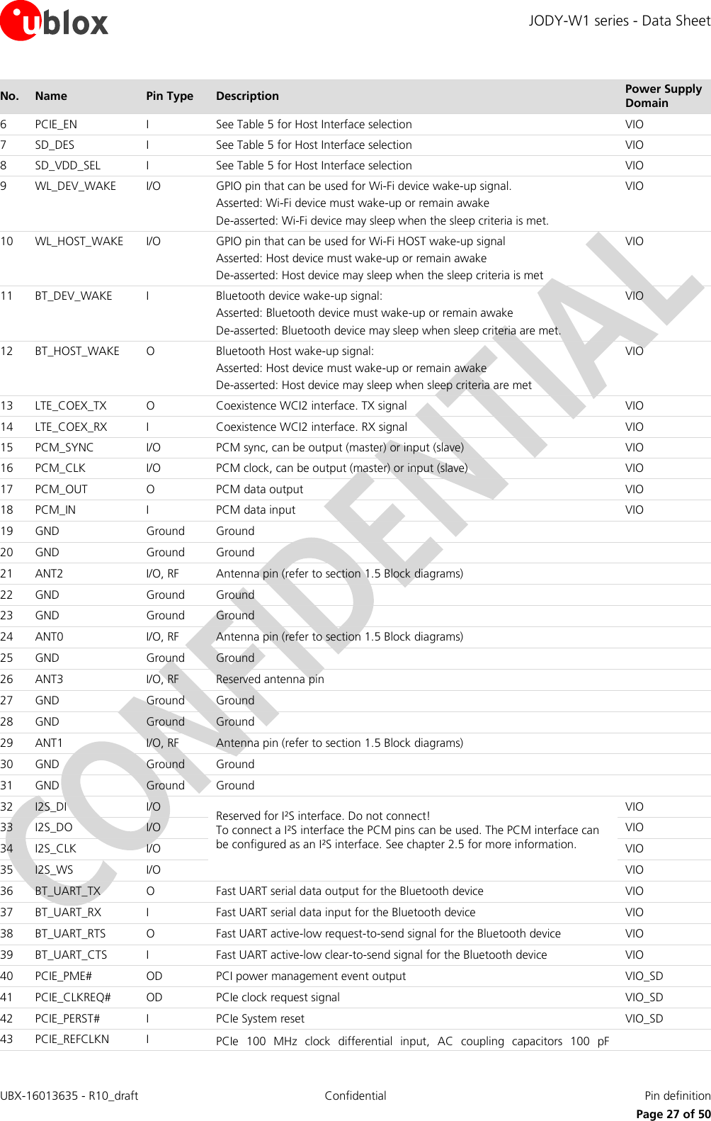
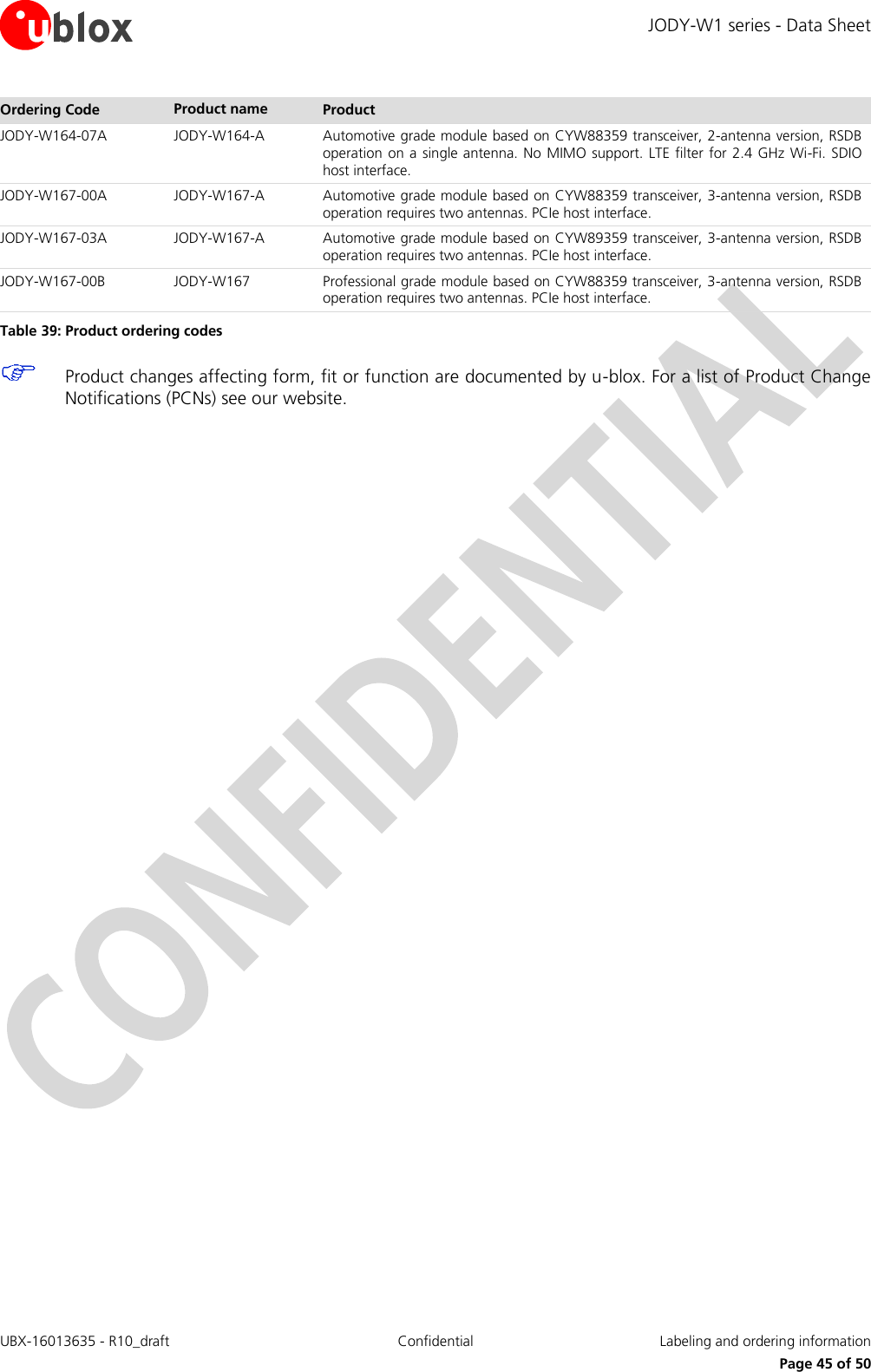
![JODY-W1 series - Data Sheet UBX-16013635 - R10_draft Confidential Pin definition Page 28 of 50 No. Name Pin Type Description Power Supply Domain 44 PCIE_REFCLKP I included in the module. 45 PCIE_RDN I PCIe receiver differential input, DC coupled inputs, use 100 nF AC coupling capacitors placed closer to the Host TDN/TDP differential output 46 PCIE_RDP I 47 PCIE_TDN O PCIe transmitter differential output, AC coupling capacitors 100 nF included in the module, connect to the Host RDN/RDP input directly 48 PCIE_TDP O 49 GND Ground Ground 50 SD_D2 I/O SDIO Data line bit [2] VIO_SD 51 SD_D3 I/O SDIO Data line bit [3] VIO_SD 52 SD_CMD I/O SDIO Command line VIO_SD 53 SD_CLK I SDIO Clock input VIO_SD 54 SD_D0 I/O SDIO Data line bit [0] VIO_SD 55 SD_D1 I/O SDIO Data line bit [1] VIO_SD 56 NC - Leave unconnected (internally connected to the USB interface, debugging only) 57 NC - Leave unconnected (internally connected to the USB interface, debugging only) 58 WL_EN I Power up or power down the Wi-Fi section of the chipset (like a reset) VIO 59 BT_EN I Power up or power down the Bluetooth section of the chipset (like a reset) VIO 60 LPO_IN I Clock input for external sleep clock source (32.768 kHz) EP GND Ground 15 Ground/Thermal exposed pins, connect to the ground Table 21: JODY-W1 series pin description](https://usermanual.wiki/u-blox/JODYW164.Data-Sheet/User-Guide-3927160-Page-28.png)
![JODY-W1 series - Data Sheet UBX-16013635 - R10_draft Confidential Electrical specification Page 29 of 50 4 Electrical specification Stressing the device above one or more of the ratings listed in the Absolute Maximum Rating section may cause permanent damage. These are stress ratings only. Operating the module at these or at any conditions other than those specified in the Operating conditions section of this document should be avoided. Exposure to absolute maximum rating conditions for extended periods may affect device reliability. Operating condition ranges define those limits within which the functionality of the device is guaranteed. Where application information is given, it is advisory only and does not form part of the specification. 4.1 Absolute maximum ratings Symbol Description Min. Max. Units VBAT Power supply voltage -0.5 6.0 V VIO I/O supply voltage 1.8V/3.3V -0.5 3.9 V VIO_SD SDIO supply voltage 1.8V/3.3V -0.5 3.9 V TSTORAGE Storage temperature -40 +85 ºC Table 22: Absolute maximum ratings The product is not protected against overvoltage or reversed voltages. If necessary, voltage spikes exceeding the power supply voltage specification, given in table above, must be limited to values within the specified boundaries by using appropriate protection devices. 4.2 Operating conditions Symbol Parameter Min. Typ Max. Units VBAT Power supply voltage 3.2 - 4.8 V VIO I/O supply voltage 1.8V/3.3V 1.62 - 3.63 V VIO_SD SDIO supply voltage 1.8V/3.3V 1.62 - 3.63 V TA Ambient operating temperature -40 - +85 ºC Ripple Noise Peak-to-peak voltage ripple on VBAT and VIO supply lines. - - 10 mV Table 23: Operating conditions For temperature above 55 °C, the radio transceiver autonomously monitors its junction temperature and employs transmit duty cycle throttling to regulate power dissipation and thereby ensures that the junction temperature is safely below 115 °C. Transmit duty cycle throttling can lower throughput to up to 25% of maximum throughput at nominal temperature. 4.3 Digital pad ratings The following ratings are only for the SDIO interface I/O Pins and PCIe Out-of-Band signals (PCIE_PERST_L, PCIE_PME_L and PCIE_CLKREQ_L).](https://usermanual.wiki/u-blox/JODYW164.Data-Sheet/User-Guide-3927160-Page-29.png)
![JODY-W1 series - Data Sheet UBX-16013635 - R10_draft Confidential Electrical specification Page 30 of 50 Symbol Parameter VIO_SD Min. Max. Units VIH Input high voltage 1.8 V 1.27 - V 3.3 V 0.625*VIO_SD - V VIL Input low voltage 1.8 V - 0.58 V 3.3 V - 0.25*VIO_SD V VOH Output high voltage @ 2mA 1.8 V 1.4 - V 3.3 V 0.75*VIO_SD - V VOH Output low voltage @ 2mA 1.8 V - 0.45 V 3.3 V - 0.125*VIO_SD V Table 24: DC characteristics SDIO digital I/O pins The following ratings are for all other digital I/O pins including GPIOs. Symbol Parameter VIO Min. Max. Units VIH Input high voltage 1.8 V 0.65*VIO - V 3.3 V 2.0 - V VIL Input low voltage 1.8 V - 0.35*VIO V 3.3 V - 0.8 V VOH Output high voltage @ 2mA 1.8 V VIO-0.45 - V 3.3 V VIO-0.4 - V VOH Output low voltage @ 2mA 1.8 V - 0.45 V 3.3 V - 0.4 V Table 25: DC characteristics digital I/O pins 4.4 Wi-Fi power consumption Operation mode: 2.4 GHz and 5 GHz Wi-Fi, BT powered down Typical VBAT (3.3 V) current, mA Typical VBAT (3.3 V) idle current, mA Typical VIO (1.8 V) idle current, µA TX modes CCK 11 Mbps, BW20, Ch7, Core2, 18dBm 360 110 60 MSC7, HT20 , Ch7, Core2, 14dBm 270 110 60 BPSK, 6 Mbps, HT20, Ch100, Core1, 17dBm 520 135 60 BPSK, 6 Mbps, HT20, Ch100, Core2, 17dBm 450 135 60 MCS7, HT20, SGI, CH100, Core1, 14dBm 440 135 60 MCS7, HT20, SGI, CH100, Core2, 14dBm 420 135 60 MCS7, HT40, SGI, Ch100, Core1, 14dBm 460 165 60 MCS7, HT40, SGI, Ch100, Core2, 14dBm 430 165 60 MCS9, VHT40, SGI, Ch100, Core1, 12dBm 430 165 60 MCS9, VHT40, SGI, Ch100, Core2, 12dBm 420 165 60 MCS9, VHT80, SGI, Ch100, Core1, 12dBm 470 240 60 MCS9, VHT80, SGI, Ch100, Core2, 12dBm 470 240 60 MCS9, VHT40, SGI, Ch100, 2 streams, 12dBm 760 165 60 MCS9, VHT80, SGI, Ch100, 2 streams, 12dBm 820 240 60 RX modes MCS7, HT40, Ch100, Core2 190 165 60 MCS7, HT20, Ch7, Core2 120 110 60 1 Mbps, BW20, Ch7, Core2 110 110 60 6 Mbps, BW20, Ch100, Core2 140 135 60 MCS7, HT20, Ch100, Core2 140 135 60 MCS7, HT20, Ch100, Core1 140 135 60 MCS0, HT80, Ch100, Core1 245 240 60 Table 26: Current consumption for different Wi-Fi TX- and RX-modes at 25 °C](https://usermanual.wiki/u-blox/JODYW164.Data-Sheet/User-Guide-3927160-Page-30.png)
![JODY-W1 series - Data Sheet UBX-16013635 - R10_draft Confidential Electrical specification Page 31 of 50 Operation mode: Power save modes Typical VBAT (3.3 V) current, µA Typical VIO (1.8 V) current, µA Sleep (Idle, not associated), FW loaded 5.3 180 wlan power save, dtim 1 2600 220 wlan power save, dtim 2 1300 220 wlan power save, dtim 3 900 220 Table 27: Current consumption for Wi-Fi power-save modes at 25 °C 4.5 Bluetooth power consumption Operation mode: Bluetooth mode with Wi-Fi powered down Typical VBAT (3.3 V) current, µA Typical VIO (1.8 V) current, µA Typical VIO (3.3 V) current, µA Sleep 5.3 130 170 Standard 1.28s inquiry scan 150 150 185 DM5/DH5 56000 40 50 BLE scan 160 150 185 BLE advertising, unconnectable 1 sec 60 150 185 Table 28: Current consumption for Bluetooth operation at 25 °C 4.6 Radio specifications 4.6.1 Wi-Fi The JODY-W1 series modules support dual-band Wi-Fi with 802.11a/b/g/n/ac operation in the 2.4 GHz and 5 GHz radio bands. The values in the table are design goals for the chipset and can be used for comparing with the JODY-W1 prototype values. Parameter Operation Mode Specification RF Frequency range 802.11b/g/n 2.400 – 2.500 GHz 802.11a/n/ac 4.900 – 5.845 GHz Modulation 802.11b CCK and DSSS 802.11a/g/n/ac OFDM Supported data rates 802.11b 1, 2, 5.5, 11 Mbps 802.11a/g 6, 9, 12, 18, 24, 36, 48, 54 Mbps 802.11n SISO MCS0 - MCS7 (150 Mbps) 802.11n MIMO MCS8 – MCS15 (300 Mbps) 802.11ac SISO MCS0 – MCS9 (433 Mbps) 802.11ac MIMO MCS0 – MCS9 (867 Mbps) Supported channel bandwidth 2.4 GHz band 5 GHz band 20 MHz 20, 40, 80 MHz Supported guard interval (GI) 802.11n 400, 800 ns 802.11ac Short guard interval supported Parameter Operation Mode 802.11 EVM limit Specification (typ. output power tolerance ± 2 dB) Maximum transmit power 2.4 GHz DSSS/CCK -9 dB 18 dBm OFDM, BPSK -8 dB 15 dBm OFDM, QPSK -13 dB 15 dBm OFDM, 16-QAM -19 dB 15 dBm OFDM, 64-QAM, 3/4 -25 dB 13 dBm OFDM, 64-QAM, 5/6 -28 dB 13 dBm 5 GHz OFDM, BPSK -8 dB 15 dBm](https://usermanual.wiki/u-blox/JODYW164.Data-Sheet/User-Guide-3927160-Page-31.png)
![JODY-W1 series - Data Sheet UBX-16013635 - R10_draft Confidential Electrical specification Page 32 of 50 OFDM, QPSK -13 dB 15 dBm OFDM, 16-QAM -19 dB 15 dBm OFDM, 64-QAM, 3/4 -25 dB 13 dBm OFDM, 64-QAM, 5/6 -28 dB 13 dBm OFDM, 256-QAM, 3/4 -30 dB 8 dBm OFDM, 256-QAM, 5/6 -32 dB 8 dBm Parameter Operation Mode Specification Receiver sensitivity 2.4 GHz 802.11b 1 Mbps -98 dBm ± 1 dB 11 Mbps -90 dBm ± 1 dB 802.11g SISO 6 Mbps -95 dBm ± 1 dB 54 Mbps -78 dBm ± 1 dB 802.11n SISO 20 MHz MCS0 -95 dBm ± 1 dB MCS7 -75 dBm ± 1 dB 802.11n MIMO 20 MHz MCS0 -96 dBm ± 1 dB MCS7 -79 dBm ± 1 dB 5 GHz 802.11n SISO 40 MHz MCS0 -89 dBm ± 1 dB MCS7 -70 dBm ± 1 dB 802.11n MIMO 40 MHz MCS8 -90 dBm ± 1 dB / core MCS15 -70 dBm ± 1 dB / core 802.11ac SISO 20 MHz MCS0 -92 dBm ± 1 dB MCS8 -68 dBm ± 1 dB 802.11ac MIMO 20 MHz MCS0 -92 dBm ± 1 dB / core MCS8 -68 dBm ± 1 dB / core 802.11ac SISO 40 MHz MCS0 -89 dBm ± 1 dB MCS9 -64 dBm ± 1 dB 802.11ac MIMO 40 MHz MCS0 -89 dBm ± 1 dB / core MCS9 -64 dBm ± 1 dB / core 802.11ac SISO 80 MHz MCS0 -86 dBm ± 1 dB MCS9 -60 dBm ± 1 dB 802.11ac MIMO 80 MHz MCS0 -86 dBm ± 1 dB / core MCS9 -60 dBm ± 1 dB / core Table 29: Wi-Fi Radio parameters 4.6.2 Bluetooth Parameter Specifications RF Frequency Range 2.402 – 2.480 GHz Supported Modes Bluetooth v4.2+EDR Number of channels 79 Modulation 1 Mbps: GFSK (BDR) 2 Mbps: π/4 DQPSK (EDR) 3 Mbps: 8DQPSK (EDR) Transmit Power +9 dBm ± 2 dB Receiver Sensitivity BDR: -93 dBm ± 1.5 dB EDR: -89 dBm ± 1.5 dB BLE: -95 dBm ± 1.5 dB Table 30: Bluetooth radio parameters](https://usermanual.wiki/u-blox/JODYW164.Data-Sheet/User-Guide-3927160-Page-32.png)
![JODY-W1 series - Data Sheet UBX-16013635 - R10_draft Confidential Host drivers and firmware Page 33 of 50 5 Host drivers and firmware 5.1 General principle The JODY-W1 series module does not contain any persistent software. A firmware binary will be downloaded by the host operating system driver on system start-up. 5.2 Supported operating systems 5.2.1 Linux Linux device drivers are available free of charge from the chipset manufacturer. A Software License Agreement (SLA) must be signed with the chipset manufacturer to obtain the driver package. This package includes: Dedicated Kernel driver, to bind the Wi-Fi device to the kernel. The driver sources will be provided. A dedicated Wi-Fi firmware image, which will be uploaded during initialization of the Wi-Fi device. A dedicated Bluetooth firmware image, which will be uploaded during initialization of the Bluetooth device. Laboratory and manufacturing tools. For a detailed description of the driver packages, refer to JODY-W1 series System Integration Manual [2].](https://usermanual.wiki/u-blox/JODYW164.Data-Sheet/User-Guide-3927160-Page-33.png)
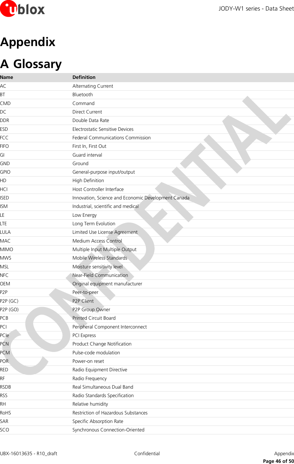
![JODY-W1 series - Data Sheet UBX-16013635 - R10_draft Confidential Mechanical specifications Page 34 of 50 6 Mechanical specifications Figure 19: JODY-W1 series dimensions (bottom view) Parameter Description Typical Tolerance A Module Length [mm] 19.8 (779.5 mil) +0.35/-0.1 (+13.8/-3.9 mil) B Module Width [mm] 13.8 (543.3 mil) +0.1/-0.1 (+3.9/-3.9 mil) C Module Thickness [mm] 2.5 (98.4 mil) +0.2/-0.2 (+7.9/-7.9 mil) ccc Seating Plane Coplanarity [mm] <0.1 (3.94 mil) D PCB Edge to Pin Edge [mm] 0.3 (11.8 mil) +0.20/-0.20 (+7.9/-7.9 mil) E Pin Width [mm] 0.7 (27.6 mil) +0.05/-0.05 (+2.0/-2.0 mil) F Pin Length [mm] 0.95 (37.4 mil) +0.05/-0.05 (+2.0/-2.0 mil) G Pin to Pin Pitch [mm] 1.0 (39.4 mil) +0.02/-0.02 (+0.8/-0.8 mil) H Horizontal Corner Pin to Pin Pitch [mm] 1.125 (44.3 mil) +0.02/-0.02 (+0.8/-0.8 mil) I Lateral Corner Pin to Pin Pitch [mm] 1.125 (44.3 mil) +0.02/-0.02 (+0.8/-0.8 mil) J Horizontal Thermal Pads Pitch [mm] 3.2 (126.0 mil) +0.02/-0.02 (+0.8/-0.8 mil) K Thermal Pad Height [mm] 2.2 (86 6 mil) +0.1/-0.1 (+3.9/-3.9 mil) L Thermal Pad Length [mm] 2.7 (106.3 mil) +0.1/-0.1 (+3.9/-3.9 mil) M Pin 1 Diameter [mm] 0.95 (37.4 mil) +0.05/-0.05 (+2.0/-2.0 mil) N Horizontal Pin to Thermal Pad Pitch [mm] 3.425 (134.8 mil) +0.02/-0.02 (+0.8/-0.8 mil) O Lateral Pin to Thermal Pad Distance [mm] 2.725 (107.3 mil) +0.02/-0.02 (+0.8/-0.8 mil) P Lateral Thermal Pads Pitch [mm] 2.7 (106.3 mil) +0.02/-0.02 (+0.8/-0.8 mil) R Reserved area for future module variants 1.55 (61.0 mil) +0.05/-0.05 (+2.0/-2.0 mil) DEFHDD OGGEDAIBFFLKMJSeatingcccPlaneCHPin1J PNPNOJKeep this area free of copper*Keep this area free of copper*RR*Future module variants can have more pins in this area. To ensure compatibility this area should be kept free of copper.](https://usermanual.wiki/u-blox/JODYW164.Data-Sheet/User-Guide-3927160-Page-34.png)
![JODY-W1 series - Data Sheet UBX-16013635 - R10_draft Confidential Approvals Page 35 of 50 7 Approvals The JODY-W1 series modules comply with the regulatory demands of Federal Communications Commission (FCC), Industry Canada (IC) and the CE mark6. See JODY-W1 series System Integration Manual [2] to obtain information and requirements regarding regulatory compliance of end-products using JODY-W1 series module. Products marked with this lead-free symbol on the product label comply with the "Directive 2002/95/EC of the European Parliament and the Council on the Restriction of Use of certain Hazardous Substances in Electrical and Electronic Equipment" (RoHS). JODY-W1 series Wi-Fi/Bluetooth multi-radio modules are RoHS compliant. No natural rubbers, hygroscopic materials, or materials containing asbestos are employed. All certifications and approvals mentioned below have not been completed yet and are in the final stage currently. 7.1 European Union regulatory compliance The JODY-W1 series module complies with the following regulatory standards: Essential Requirements Radio Equipment Directive 2014/53/EU Standards Safety & Health (Article 3.1a) IEC 60950-1:2005 (2nd Edition) + A1:2009 EN 60950-1:2006 + A11:2009 + A1:2010 + A12:2011 EN 62311:2008 (Wi-Fi) EN 62479:2010 (Bluetooth) EMC (Article 3.1b) EN 301 489-1 V2.1.1 EN 301 489-17 V3.1.1 Radio Spectrum Efficiency (Article 3.2) EN 300 328 V2.1.1 EN 301 893 V2.1.1 EN 300 440 V2.1.1 Essential Requirements RoHS Directive 2011/65/EU Standards Prevention (Article 4.1) EN 50581:2012 7.2 FCC and IC compliance This section contains the FCC and IC compliance information for the JODY-W1 series module. 6 Approvals are pending.](https://usermanual.wiki/u-blox/JODYW164.Data-Sheet/User-Guide-3927160-Page-35.png)
![JODY-W1 series - Data Sheet UBX-16013635 - R10_draft Confidential Approvals Page 36 of 50 7.2.1 FCC and ISED IDs Model8 FCC ID ISED ID JODY-W163-04A, JODY-W163-05A, JODY-W164-04A, JODY-W164-05A, tbd tbd JODY-W164-03A XPYJODYW164 8595A-JODYW164 JODY-W164-07A XPYJODYW164-07A 8595A-JODYW16407A JODY-W167-00A, JODY-W167-03A, JODY-W167-00B XPYJODYW167 8595A-JODYW167 Table 31: FCC and IC IDs for different models of JODY-W1 series modules 7.2.2 FCC compliance statement The JODY-W1 series modules have modular approval, and comply with Part 15 of the FCC Rules. Operation is subject to the following two conditions: 1. This device may not cause harmful interference, and 2. This device must accept any interference received, including interference that may cause undesired operation Any changes or modifications NOT explicitly APPROVED by u-blox could cause the JODY-W1 series module to cease to comply with FCC rules part 15 thus void the user's authority to operate the equipment. The internal / external antenna(s) used for this module must provide a separation distance of at least 20 cm from all persons and must not be co-located or operating in conjunction with any other antenna or transmitter. In accordance with 47 CFR § 15.19, the end product into which this module is integrated shall bear the following statement in a conspicuous location on the device: “This device complies with Part 15 of the FCC Rules. Operation is subject to the following two conditions: 1. This device may not cause harmful interference, and 2. This device must accept any interference received, including interference that may cause undesired operation.” When the end-product is so small or for such use that it is not practical to place the above statement on it, the information shall be placed in a prominent location in the instruction manual or pamphlet supplied to the user or on the container in which the device is marketed. However, the FCC ID label must be displayed on the device. If the end-product will be installed in locations where the end-user is not able to see the FCC ID and/or this statement, the FCC ID and the statement shall also be included in the end-product manual. The outside of final products containing the JODY-W1 module must display in a user accessible area a label referring to the enclosed module9. This exterior label can use wording such as the following: “Contains Transmitter Module FCC ID: XPYJODYW164” or “Contains FCC ID: XPYJODYW164”. 7.2.3 ISED compliance statement The JODY-W1 series module complies with ISED (Innovation, Science and Economic Development Canada)11 license-exempt RSSs. Operation is subject to the following two conditions: 8 The model name is identical to the ordering code (cf. Table 39) 9 The FCC and IC IDs for the JODY-W1 series module variants are shown in . Select the applicable ID.](https://usermanual.wiki/u-blox/JODYW164.Data-Sheet/User-Guide-3927160-Page-36.png)
![JODY-W1 series - Data Sheet UBX-16013635 - R10_draft Confidential Approvals Page 37 of 50 (1) This device may not cause interference, and (2) This device must accept any interference, including interference that may cause undesired operation of the device. Any notification to the end user of installation or removal instructions about the integrated radio module is NOT allowed. Unauthorized modification could void authority to use this equipment. This equipment complies with ISED RSS-102 radiation exposure limits set forth for an uncontrolled environment. This equipment should be installed and operated with minimum distance 20 cm between the radiator and your body. This radio transmitter IC: 8595A-JODYW164 / IC: 8595A-JODYW16407A / IC: 8595A-JODYW167 has been approved by ISED to operate with the antenna types listed below with the maximum permissible gain indicated. Antenna types not included in this list, having a gain greater than the maximum gain indicated for that type, are strictly prohibited for use with this device. Operation in the band 5150–5250 MHz is only for indoor use to reduce the potential for harmful interference to co-channel mobile satellite systems; Operation in the 5600-5650 MHz band is not allowed in Canada. High-power radars are allocated as primary users (i.e. priority users) of the bands 5250-5350 MHz and 5650-5850 MHz and that these radars could cause interference and/or damage to LE-LAN devices. The ISED certification label of a module shall be clearly visible at all times when installed in the host device; otherwise, the host device must be labeled to display the ISED certification number for the module, preceded by the words “Contains transmitter module”, or the word “Contains”, or similar wording expressing the same meaning, as follows: “Contains transmitter module IC: 8595A-JODYW164”12. Le présent appareil est conforme aux CNR d'ISED applicables aux appareils radio exempts de licence. L'exploitation est autorisée aux deux conditions suivantes: (1) l'appareil ne doit pas produire de brouillage, et (2) l'utilisateur de l'appareil doit accepter tout brouillage radioélectrique subi, même si le brouillage est susceptible d'en compromettre le fonctionnement. Cet équipement est conforme aux limites d'exposition de rayonnement d'ISED RSS-102 déterminées pour un environnement non contrôlé. Cet équipement devrait être installé et actionné avec la distance minimum 20 cm entre le radiateur et votre corps. Cet émetteur radio, IC: 8595A-JODYW164 / IC: 8595A-JODYW16407A / IC: 8595A-JODYW167 été approuvé par ISED pour fonctionner avec les types d’antenne énumérés ci-dessous avec le gain maximum autorisé et l’impédance nécessaire pour chaque type d’antenne indiqué. Les types d’antenne ne figurant pas dans cette liste et ayant un gain supérieur au gain maximum indiqué pour ce type-là sont strictement interdits d’utilisation avec cet appareil. Le dispositif de fonctionnement dans la bande 5150-5250 MHz est réservé à une utilisation en intérieur pour réduire le risque d'interférences nuisibles à la co-canal systèmes mobiles par satellite Opération dans la bande 5600-5650 MHz n'est pas autorisée au Canada. Haute puissance radars sont désignés comme utilisateurs principaux (c.-àutilisateurs prioritaires) des bandes 5250-5350 MHz et 5650-5850 MHz et que ces radars pourraient causer des interférences et / ou des dommages à dispositifs LAN-EL. L’étiquette d’homologation d’ISED d’un module donné doit être posée sur l’appareil hôte à un endroit bien en vue en tout temps. En l’absence d’étiquette, l’appareil hôte doit porter une étiquette sur laquelle figure le numéro d’homologation du module d’ISED, précédé des mots « Contient un module d’émission », ou du mot « Contient », ou d’une formulation similaire allant dans le même sens et qui va comme suit : « Contient le module d’émission IC: 8595A-JODYW164 ». 11 Formerly known as IC (Industry Canada). 12 The FCC and IC IDs for the JODY-W1 series module variants are shown in . Select the applicable ID.](https://usermanual.wiki/u-blox/JODYW164.Data-Sheet/User-Guide-3927160-Page-37.png)
![JODY-W1 series - Data Sheet UBX-16013635 - R10_draft Confidential Approvals Page 38 of 50 This radio transmitter IC: 8595A-JODYW164 / IC: 8595A-JODYW16407A / IC: 8595A-JODYW167 has been approved by ISED to operate with the antenna types listed below with the maximum permissible gain indicated. Antenna types not included in this list, having a gain greater than the maximum gain indicated for that type, are strictly prohibited for use with this device. Le présent émetteur radio IC: 8595A-JODYW164 / IC: 8595A-JODYW16407A / IC: 8595A-JODYW167 a été approuvé par ISED pour fonctionner avec les types d'antenne énumérés ci-dessous et ayant un gain admissible maximal. Les types d'antenne non inclus dans cette liste, et dont le gain est supérieur au gain maximal indiqué, sont strictement interdits pour l'exploitation de l'émetteur. The internal / external antenna(s) used for this module must provide a separation distance of at least 20 cm from all persons and must not be co-located or operating in conjunction with any other antenna or transmitter. See section 7.3 for list of approved antennas. The approval type for all the JODY-W1 series variants is a single modular approval. Due to ISED Modular Approval Requirements (Source: RSP-100 Issue 10), any application which includes the module must be approved by the module manufacturer (u-blox). The application manufacturer must provide design data for the review procedure. 7.3 Certification in other countries Regulatory approvals for using the JODY-W1 series module in Japan, Korea, and Taiwan are pending. 7.4 Approved antennas Please refer to the JODY-W1 antenna reference design [3] for the essential specifications to be fulfilled in the end-product design to make use of the module’s radio type approval. It provides PCB layout details and electrical specifications. The approved antennas that may be connected to the JODY-W1 series module are listed in this section. 7.4.1 Wi-Fi operation For Wi-Fi operation in the 2.4 GHz band and Wi-Fi operation in the 5 GHz band, the JODY-W1 series module has been tested and approved for use with the antennas listed in Table 34. Manufacturer Part Number Antenna type Peak gain [dBi] Validated Regulatory Domain 2.4 GHz band 5 GHz band Any N/A Dipole antenna 2 2 FCC/IC Any N/A Dipole antenna 0 0 ETSI Table 32: List of approved Wi-Fi antennas Important: To be compliant to FCC §15.407(a) the EIRP is not allowed to exceed 125 mW (21 dBm) at any elevation angle above 30 degrees as measured from the horizon when operated as an outdoor access point in U-NII-1 band, 5.150-5.250 GHz. 7.4.2 Bluetooth operation For Bluetooth operation, the JODY-W1 series module has been tested and approved for use with the antennas listed in Table 33. Manufacturer Part Number Antenna type Peak gain [dBi] Validated Regulatory Domain 2.4 GHz band 5 GHz band Any N/A Dipole antenna 2 2 FCC/IC Any N/A Dipole antenna 0 0 ETSI](https://usermanual.wiki/u-blox/JODYW164.Data-Sheet/User-Guide-3927160-Page-38.png)
![JODY-W1 series - Data Sheet UBX-16013635 - R10_draft Confidential Approvals Page 39 of 50 Table 33: List of approved Bluetooth antennas 7.5 Bluetooth qualification13 The JODY-W1 series module is Bluetooth qualified as “Controller Subsystem”. This means that you do not need to do any further qualification if the module is combined with a host stack that is Bluetooth qualified as "Host Subsystem". 7.5.1 Bluetooth host stack Several Bluetooth host stacks are available in the market. These host stacks are suited for different tasks and environments. These host stacks could differ based on their system requirements, supported Bluetooth profiles, cost, Bluetooth qualification, support and so on. 13 Bluetooth SIG listing is pending.](https://usermanual.wiki/u-blox/JODYW164.Data-Sheet/User-Guide-3927160-Page-39.png)
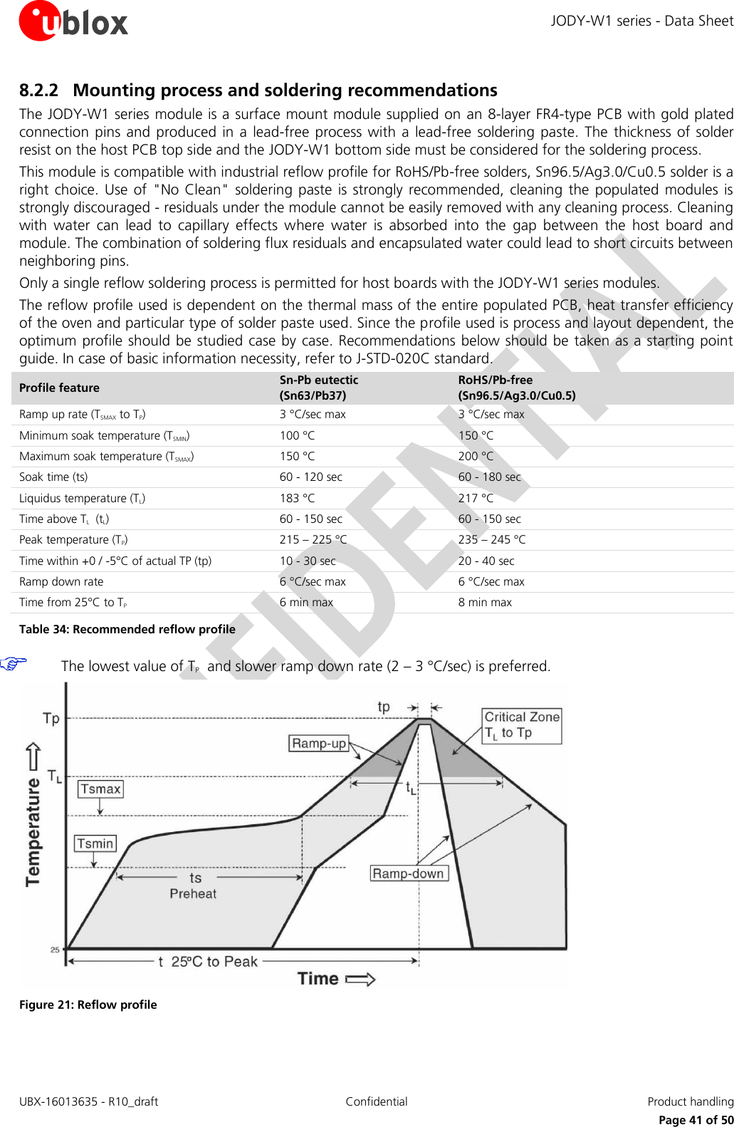
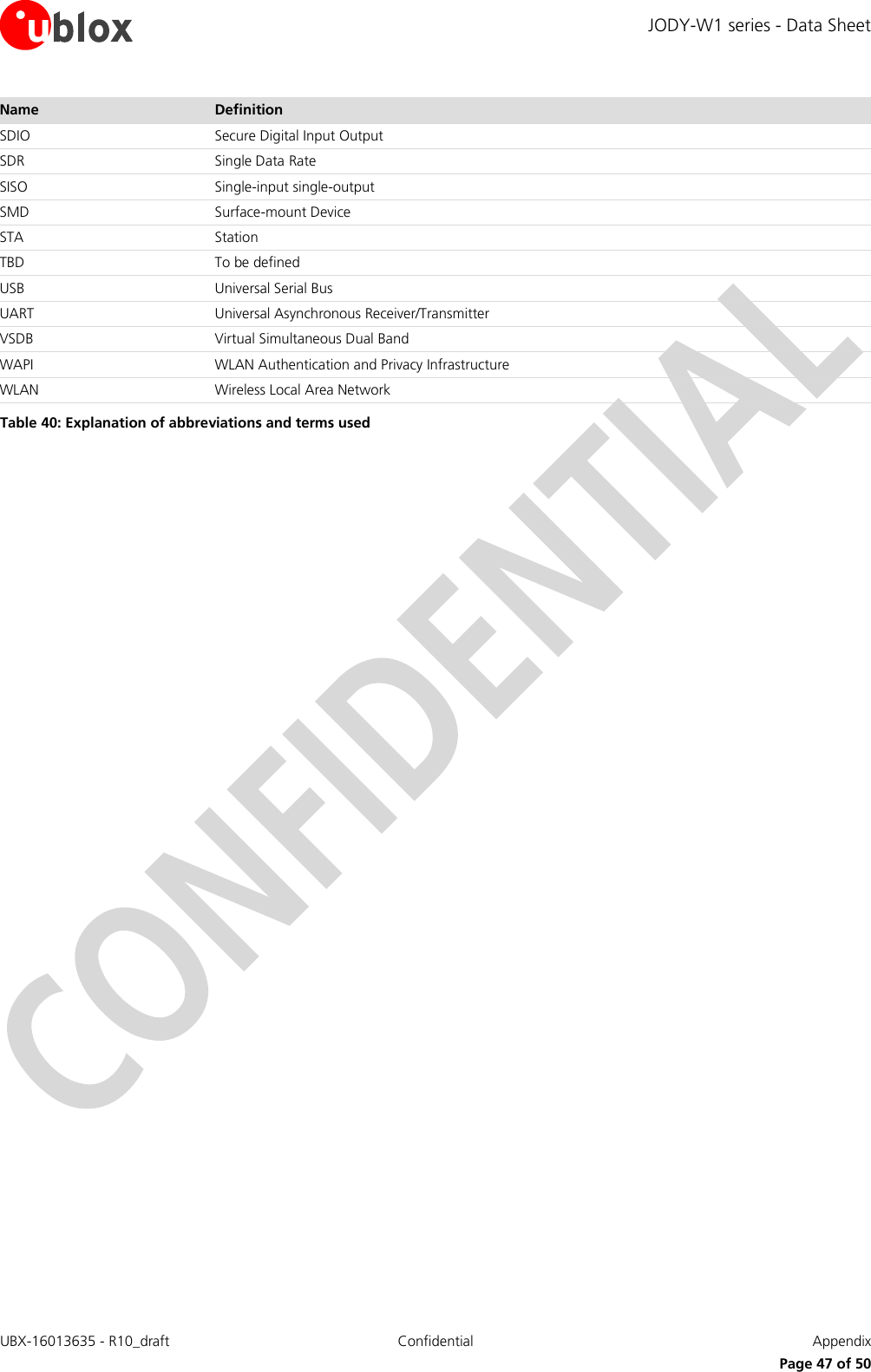
![JODY-W1 series - Data Sheet UBX-16013635 - R10_draft Confidential Product handling Page 40 of 50 8 Product handling 8.1 Packaging The JODY-W1 series modules are delivered as hermetically sealed tape and reels, to enable efficient production, production lot set-up and tear-down. For more information about packaging, see the u-blox Package Information Guide [1]. 8.1.1 Reels The JODY-W1 series modules are deliverable in quantities of 500 pieces on a reel. The JODY-W1 series modules are shipped on reel Type A as described in the u-blox Package Information Guide [1]. 8.1.2 Tapes The dimensions of the tapes are specified in Figure 20. Figure 20: JODY-W1 Tape dimensions 8.2 Shipment, storage and handling For more information regarding shipment, storage and handling see the u-blox Package Information Guide [1]. 8.2.1 Moisture sensitivity levels The JODY-W1 series automotive-grade modules are rated at moisture sensitivity level 3. See moisture sensitive warning label on each shipping bag for detailed information. After opening the dry pack, modules must be mounted within 168 hours in factory conditions of maximum 30 °C/60%RH or must be stored at less than 10%RH. Modules require baking if the humidity indicator card shows more than 10% when read at 23±5°C or if the conditions mentioned above are not met. Please refer to J-STD-033B standard for bake procedure.](https://usermanual.wiki/u-blox/JODYW164.Data-Sheet/User-Guide-3927160-Page-40.png)
![JODY-W1 series - Data Sheet UBX-16013635 - R10_draft Confidential Product handling Page 41 of 50 8.2.2 Mounting process and soldering recommendations The JODY-W1 series module is a surface mount module supplied on an 8-layer FR4-type PCB with gold plated connection pins and produced in a lead-free process with a lead-free soldering paste. The thickness of solder resist on the host PCB top side and the JODY-W1 bottom side must be considered for the soldering process. This module is compatible with industrial reflow profile for RoHS/Pb-free solders, Sn96.5/Ag3.0/Cu0.5 solder is a right choice. Use of "No Clean" soldering paste is strongly recommended, cleaning the populated modules is strongly discouraged - residuals under the module cannot be easily removed with any cleaning process. Cleaning with water can lead to capillary effects where water is absorbed into the gap between the host board and module. The combination of soldering flux residuals and encapsulated water could lead to short circuits between neighboring pins. Only a single reflow soldering process is permitted for host boards with the JODY-W1 series modules. The reflow profile used is dependent on the thermal mass of the entire populated PCB, heat transfer efficiency of the oven and particular type of solder paste used. Since the profile used is process and layout dependent, the optimum profile should be studied case by case. Recommendations below should be taken as a starting point guide. In case of basic information necessity, refer to J-STD-020C standard. Profile feature Sn-Pb eutectic (Sn63/Pb37) RoHS/Pb-free (Sn96.5/Ag3.0/Cu0.5) Ramp up rate (TSMAX to TP) 3 °C/sec max 3 °C/sec max Minimum soak temperature (TSMIN) 100 °C 150 °C Maximum soak temperature (TSMAX) 150 °C 200 °C Soak time (ts) 60 - 120 sec 60 - 180 sec Liquidus temperature (TL) 183 °C 217 °C Time above TL (tL) 60 - 150 sec 60 - 150 sec Peak temperature (TP) 215 – 225 °C 235 – 245 °C Time within +0 / -5°C of actual TP (tp) 10 - 30 sec 20 - 40 sec Ramp down rate 6 °C/sec max 6 °C/sec max Time from 25°C to TP 6 min max 8 min max Table 34: Recommended reflow profile The lowest value of TP and slower ramp down rate (2 – 3 °C/sec) is preferred. Figure 21: Reflow profile](https://usermanual.wiki/u-blox/JODYW164.Data-Sheet/User-Guide-3927160-Page-41.png)
![JODY-W1 series - Data Sheet UBX-16013635 - R10_draft Confidential Product handling Page 42 of 50 8.2.3 ESD handling precautions JODY-W1 series modules are Electrostatic Sensitive Devices (ESD). Observe precautions for handling! Failure to observe these precautions can result in severe damage to the Wi-Fi receiver! Wi-Fi transceivers are Electrostatic Sensitive Devices (ESD) and require special precautions when handling. Particular care must be exercised when handling patch antennas, due to the risk of electrostatic charges. In addition to standard ESD safety practices, the following measures should be taken into account whenever handling the receiver: Unless there is a galvanic coupling between the local GND (i.e. the work table) and the PCB GND, then the first point of contact when handling the PCB must always be between the local GND and PCB GND. Before mounting an antenna patch, connect ground of the device When handling the RF pin, do not come into contact with any charged capacitors and be careful when contacting materials that can develop charges (e.g. patch antenna ~10 pF, coax cable ~50-80 pF/m, soldering iron, …) To prevent electrostatic discharge through the RF input, do not touch any exposed antenna area. If there is any risk that such exposed antenna area is touched in non ESD protected work area, implement proper ESD protection measures in the design. When soldering RF connectors and patch antennas to the receiver’s RF pin, make sure to use an ESD safe soldering iron (tip).](https://usermanual.wiki/u-blox/JODYW164.Data-Sheet/User-Guide-3927160-Page-42.png)
![JODY-W1 series - Data Sheet UBX-16013635 - R10_draft Confidential Labeling and ordering information Page 43 of 50 9 Labeling and ordering information 9.1 Product labeling The labels of JODY-W1 series include important product information as described in this section. The data matrix code for automotive and professional grade variants of JODY-W1 series includes a serial number. Figure 22 illustrates the sample label of the JODY-W1 series and includes: the u-blox logo, product name (model), type number, FCC and IC certification number and date of unit production encoded YY/WW (year/week). Figure 22: JODY-W1 series sample label A detailed description of the label components are listed in Table 35. Reference Description 1 Text in bold font: MODEL: type number without the product version 2 Product version (“xxB-yy” for professional and “xxA-yy” for automotive grade) 3 Date of production encoded YY/WW (year/week) 4 FCC/ISED ID which the module has been listed with 5 Data Matrix with unique serial number of 19 alphanumeric symbols. The 3 first symbols represent the unique module type no, the next 12 symbols represent the unique hexadecimal Bluetooth MAC address of the module in the format AABBCCDDEEFF, and the last 4 symbols represent the hardware and firmware version encoded HHFF. 6 u-blox logo, the red dot in the logo is also marking pin no 1 Table 35: JODY-W1 series label description The model name, which is identical to the ordering code, used for product type approval is shown on the first line of the label. Table 36 provides the mapping of ordering code, label contents and FCC/ISED IDs. The marking “yy” in Reference 2 on the label is the minor product version and not relevant for certification. Ordering code Label marking FCC ID ISED ID Ref. 1 (Model: …) Ref. 2 JODY-W163-04A, JODY-W163-05A, JODY-W163 JODY-W163 04A-yy 05A-yy tbd tbd 1 2 3 4 5 6](https://usermanual.wiki/u-blox/JODYW164.Data-Sheet/User-Guide-3927160-Page-43.png)
![JODY-W1 series - Data Sheet UBX-16013635 - R10_draft Confidential Labeling and ordering information Page 44 of 50 Ordering code Label marking FCC ID ISED ID Ref. 1 (Model: …) Ref. 2 JODY-W164-04A, JODY-W164-05A, JODY-W164 JODY-W164 04A-yy 05A-yy JODY-W164-03A JODY-W164 03A-yy XPYJODYW164 8595A-JODYW164 JODY-W164-07A JODY-W164 07A-yy XPYJODYW164-07A 8595A-JODYW16407A JODY-W167-00A, JODY-W167-03A, JODY-W167-00B JODY-W167 JODY-W167 JODY-W167 00A-yy 03A-yy 00B-yy XPYJODYW167 8595A-JODYW167 Table 36: Mapping of ordering code, label marking and FCC/ISED IDs. 9.2 Table Explanation of codes Two different product code formats are used. The Product Name is used in documentation such as this data sheet and identifies all u-blox products, independent of packaging and quality grade. The Ordering Code includes options and quality, while the Type Number includes the hardware and firmware versions. Table 37 explains these three different formats: Format Structure Product Name PPPP-TGVV Ordering Code PPPP-TGVV-TTQ Type Number PPPP-TGVV-TTQ-XX Table 37: Product code formats Table 38 explains the parts of the product code. Code Meaning Example PPPP Form factor JODY TG Platform T – Dominant technology, For example, W: Wi-Fi, B: Bluetooth G - Generation W1 VV Variant based on the same platform; range [00…99] 61 TT Major Product Version 00 Q Quality grade A: Automotive B: Professional C: Standard A XX Minor product version (not relevant for certification) 00 Table 38: Part identification code 9.3 Ordering codes Ordering Code Product name Product JODY-W163-04A JODY-W163-A Automotive grade module based on CYW89359 transceiver, 2-antenna version, RSDB operation on a single antenna. No MIMO support. SDIO host interface. JODY-W163-05A JODY-W163-A Automotive grade module based on CYW88359 transceiver, 2-antenna version, RSDB operation on a single antenna. No MIMO support. SDIO host interface. JODY-W164-03A JODY-W164-A Automotive grade module based on CYW89359 transceiver, 2-antenna version, RSDB operation on a single antenna. Support for 5 GHz MIMO. PCIe host interface. JODY-W164-04A JODY-W164-A Automotive grade module based on CYW89359 transceiver, 2-antenna version, RSDB operation on a single antenna. No MIMO support. PCIe host interface. JODY-W164-05A JODY-W164-A Automotive grade module based on CYW88359 transceiver, 2-antenna version, RSDB operation on a single antenna. No MIMO support. PCIe host interface.](https://usermanual.wiki/u-blox/JODYW164.Data-Sheet/User-Guide-3927160-Page-44.png)
![JODY-W1 series - Data Sheet UBX-16013635 - R10_draft Confidential Labeling and ordering information Page 45 of 50 Ordering Code Product name Product JODY-W164-07A JODY-W164-A Automotive grade module based on CYW88359 transceiver, 2-antenna version, RSDB operation on a single antenna. No MIMO support. LTE filter for 2.4 GHz Wi-Fi. SDIO host interface. JODY-W167-00A JODY-W167-A Automotive grade module based on CYW88359 transceiver, 3-antenna version, RSDB operation requires two antennas. PCIe host interface. JODY-W167-03A JODY-W167-A Automotive grade module based on CYW89359 transceiver, 3-antenna version, RSDB operation requires two antennas. PCIe host interface. JODY-W167-00B JODY-W167 Professional grade module based on CYW88359 transceiver, 3-antenna version, RSDB operation requires two antennas. PCIe host interface. Table 39: Product ordering codes Product changes affecting form, fit or function are documented by u-blox. For a list of Product Change Notifications (PCNs) see our website.](https://usermanual.wiki/u-blox/JODYW164.Data-Sheet/User-Guide-3927160-Page-45.png)
![JODY-W1 series - Data Sheet UBX-16013635 - R10_draft Confidential Appendix Page 46 of 50 Appendix A Glossary Name Definition AC Alternating Current BT Bluetooth CMD Command DC Direct Current DDR Double Data Rate ESD Electrostatic Sensitive Devices FCC Federal Communications Commission FIFO First In, First Out GI Guard interval GND Ground GPIO General-purpose input/output HD High Definition HCI Host Controller Interface ISED Innovation, Science and Economic Development Canada ISM Industrial, scientific and medical LE Low Energy LTE Long Term Evolution LULA Limited Use License Agreement MAC Medium Access Control MIMO Multiple Input Multiple Output MWS Mobile Wireless Standards MSL Moisture sensitivity level NFC Near-Field Communication OEM Original equipment manufacturer P2P Peer-to-peer P2P (GC) P2P Client P2P (GO) P2P Group Owner PCB Printed Circuit Board PCI Peripheral Component Interconnect PCIe PCI Express PCN Product Change Notification PCM Pulse-code modulation POR Power-on reset RED Radio Equipment Directive RF Radio Frequency RSDB Real Simultaneous Dual Band RSS Radio Standards Specification RH Relative humidity RoHS Restriction of Hazardous Substances SAR Specific Absorption Rate SCO Synchronous Connection-Oriented](https://usermanual.wiki/u-blox/JODYW164.Data-Sheet/User-Guide-3927160-Page-46.png)
![JODY-W1 series - Data Sheet UBX-16013635 - R10_draft Confidential Appendix Page 47 of 50 Name Definition SDIO Secure Digital Input Output SDR Single Data Rate SISO Single-input single-output SMD Surface-mount Device STA Station TBD To be defined USB Universal Serial Bus UART Universal Asynchronous Receiver/Transmitter VSDB Virtual Simultaneous Dual Band WAPI WLAN Authentication and Privacy Infrastructure WLAN Wireless Local Area Network Table 40: Explanation of abbreviations and terms used](https://usermanual.wiki/u-blox/JODYW164.Data-Sheet/User-Guide-3927160-Page-47.png)
![JODY-W1 series - Data Sheet UBX-16013635 - R10_draft Confidential Related documents Page 48 of 50 Related documents [1] u-blox Package Information Guide, document number UBX-14001652 [2] JODY-W1 series System Integration Manual, document number UBX-15024929 [3] JODY-W1 antenna reference design, document number UBX-18017767 [4] Radio Equipment Directive; http://ec.europa.eu/growth/sectors/electrical-engineering/red-directive; July 2017 For regular updates to u-blox documentation and to receive product change notifications, register on our homepage (http://www.u-blox.com).](https://usermanual.wiki/u-blox/JODYW164.Data-Sheet/User-Guide-3927160-Page-48.png)
![JODY-W1 series - Data Sheet UBX-16013635 - R10_draft Confidential Revision history Page 49 of 50 Revision history Revision Date Name Comments R01 11-Jul-2016 vdyk Initial release. R02 2-Nov-2016 vdyk, ishe, este, kgom Removed support for USB interface (section 2.5). Modified the block diagram of JODY-W165 and Pin assignment (Figure 17), and Physical dimensions (Figure 18). Updated the key features (Table 1), module configuration (Table 5), and pin description of JODY-W1 series (Table 19). R03 29-Nov-2016 mhei, ddie Updated Figure 16. R04 2-Mar-2017 ddie, ishe, kgom Removed reference to JODY-W165 (Professional grade with 2 antenna pins) and included JODY-W167-A (Automotive grade with 3 antenna pins) product variant. Updated Table 1. Included information about supported RSDB and MIMO configurations (section 1.5). Corrected pin names (Figure 16). Removed Reset configuration section. Updated FCC and IC IDs (section 7.3) and ordering codes (section 9.3). Replaced document status with disclosure restriction. R05 4-May-2017 ddie, ishe, mzes, kgom Added JODY-W164-A product variant and included block diagram, FCC/IC ID, ordering code for this variant. Updated section 1.1 and Table 1. Included information about Extended operation mode configuration (section 2.1). Updated product description (1.1). Updated Figure 9 and Figure 10. Corrected pin names (Figure 18). Included detailed pin description for antenna pins. Updated Mechanical specification (section 6). Updated FCC and IC IDs (section 1.1) and ordering codes (section 9.3). R06 08-Sep-2017 mzes, ishe, shoe, ddie Updated support for 802.11 standards (section 1.7.1). Added information about PCIe pins in Table 21. Included information about RED certification (section 7.1). Added information about JODY-W164-07A. Updated JODY-W164-A block diagram (Figure 1). Added support for RSDB over SDIO. R07 23-Feb-2018 ddie, mhei, mzes, kgom Removed the product variant - JODY-W165-A and modified the product status for most of the variants to Engineering Sample in the last table on page 2. Removed support for UART H5 (section 2.4). Updated Pin definition table (Table 21), added Wi-Fi and Bluetooth current consumption specifications (Table 26, Table 27, and Table 28). Included a note with respect to temperature derating in section 4.2. Updated the mechanical specifications (Figure 19). Updated (section ). Updated the product label drawing in Section 9.1 and corrected the data matrix code content (section 9.1). R08 5-Mar-2018 mhei, kgom Updated section 1.1, Table 1 and pin assignment (top view) (Figure 18). R09 29-Mar-2018 kgom, ishe Updated Table 1. Included footnote related to support of SDIO interface for Automotive grade variants only. R10 15-Jun-2018 ishe, mzes, ddie, mhei Tables 25 and 26 updated. Added product types JODY-W163-04A, JODY-W163-05A, JODY-W167-00B. Removed all references to previously considered product types. Updated support of a single host interface only (SDIO or PCIe) per product type. Chipset information added to Document Information. Major update on Approvals section (standards references, approved antennas, Bluetooth qualification. Table 36 added.](https://usermanual.wiki/u-blox/JODYW164.Data-Sheet/User-Guide-3927160-Page-49.png)
![JODY-W1 series - Data Sheet UBX-16013635 - R10_draft Confidential Contact Page 50 of 50 Contact For complete contact information visit us at www.u-blox.com u-blox Offices North, Central and South America u-blox America, Inc. Phone: +1 703 483 3180 E-mail: info_us@u-blox.com Regional Office West Coast: Phone: +1 408 573 3640 E-mail: info_us@u-blox.com Technical Support: Phone: +1 703 483 3185 E-mail: support @u-blox.com Headquarters Europe, Middle East, Africa u-blox AG Phone: +41 44 722 74 44 E-mail: info@u-blox.com Support: support @u-blox.com Asia, Australia, Pacific u-blox Singapore Pte. Ltd. Phone: +65 6734 3811 E-mail: info_ap@u-blox.com Support: support_ap@u-blox.com Regional Office Australia: Phone: +61 2 8448 2016 E-mail: info_anz@u-blox.com Support: support_ap@u-blox.com Regional Office China (Beijing): Phone: +86 10 68 133 545 E-mail: info_cn@u-blox.com Support: support_cn@u-blox.com Regional Office China (Shenzhen): Phone: +86 755 8627 1083 E-mail: info_cn@u-blox.com Support: support_cn@u-blox.com Regional Office India: Phone: +91 80 4050 9200 E-mail: info_in@u-blox.com Support: support_in@u-blox.com Regional Office Japan: Phone: +81 3 5775 3850 E-mail: info_jp@u-blox.com Support: support_jp@u-blox.com Regional Office Korea: Phone: +82 2 542 0861 E-mail: info_kr@u-blox.com Support: support_kr@u-blox.com Regional Office Taiwan: Phone: +886 2 2657 1090 E-mail: info_tw@u-blox.com Support: support_tw@u-blox.com](https://usermanual.wiki/u-blox/JODYW164.Data-Sheet/User-Guide-3927160-Page-50.png)