u blox LISAU120 LISA-U120 User Manual LISA U1 LISA H1 series
u-blox AG LISA-U120 LISA U1 LISA H1 series
UserManual.wiki
>
u blox
>
LISAU120 User Manual
[short-term confidential] User's Manual
Navigation menu
Upload a User Manual
Namespaces
Wiki Guide
HTML
PDF
Info
Views
User Manual
Discussion / Help
Navigation

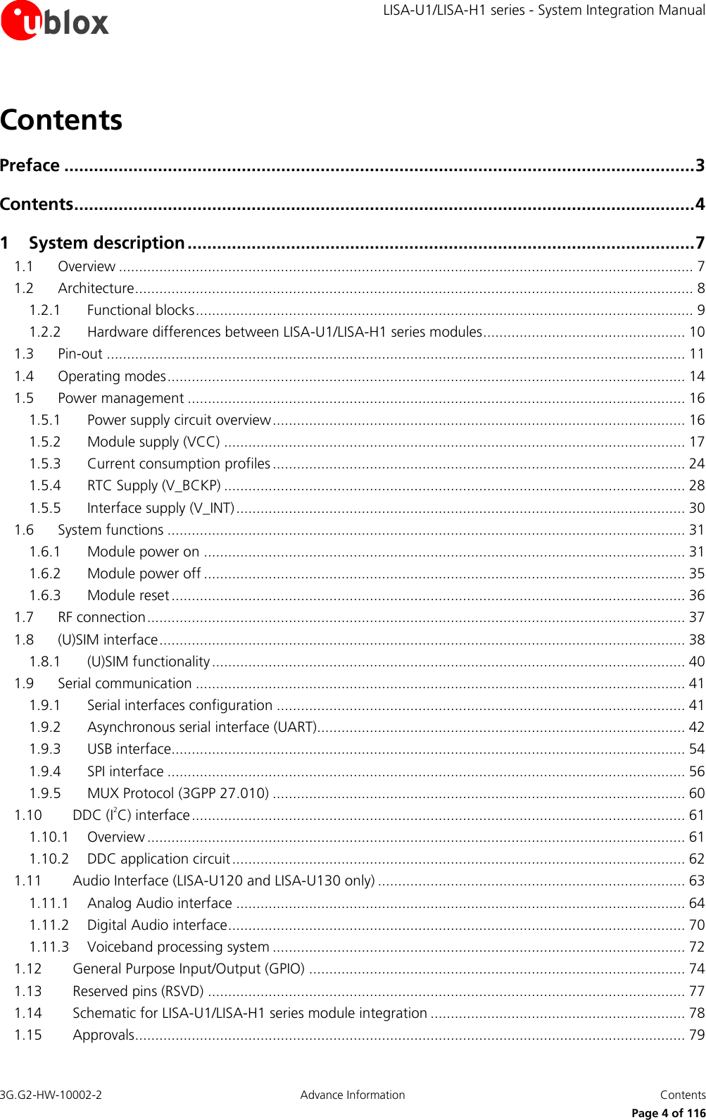

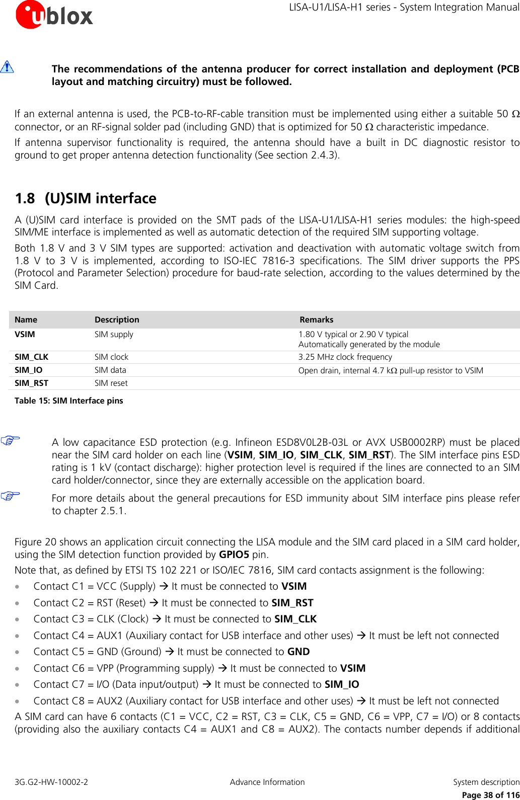
![LISA-U1/LISA-H1 series - System Integration Manual 3G.G2-HW-10002-2 Advance Information System description Page 12 of 116 Function Pin No I/O Description Remarks SPI_MRDY 59 I SPI Master Ready to transfer control line. Master Output, Slave Input Module Input: module runs as an SPI slave. Internal active pull- down to GND enabled. See section 1.9.4 DDC SCL 45 O I2C bus clock line Fixed open drain. External pull-up required. See section 1.10 SDA 46 I/O I2C bus data line Fixed open drain. External pull-up required. See section 1.10 UART RxD 16 O UART received data Circuit 104 (RxD) in ITU-T V.24. Provide access to the pin for FW update and debugging if the USB interface is connected to the application processor. See section 1.9.2 TxD 15 I UART transmitted data Circuit 103 (TxD) in ITU-T V.24. Internal active pull-up to V_INT (1.8 V) enabled. Provide access to the pin for FW update and debugging if the USB interface is connected to the application processor. See section 1.9.2 CTS 14 O UART clear to send Circuit 106 (CTS) in ITU-T V.24. Provide access to the pin for debugging if the USB interface is connected to the application processor. See section 1.9.2 RTS 13 I UART ready to send Circuit 105 (RTS) in ITU-T V.24. Internal active pull-up to V_INT (1.8 V) enabled. Provide access to the pin for debugging if the USB interface is connected to the application processor. See section 1.9.2 DSR 9 O UART data set ready Circuit 107 (DSR) in ITU-T V.24. See section 1.9.2 RI 10 O UART ring indicator Circuit 125 (RI) in ITU-T V.24. See section 1.9.2 DTR 12 I UART data terminal ready Circuit 108/2 (DTR) in ITU-T V.24. Internal active pull-up to V_INT (1.8 V) enabled. See section 1.9.2 DCD 11 O UART data carrier detect Circuit 109 (DCD) in ITU-T V.24. See section 1.9.2 GPIO GPIO1 20 I/O GPIO See section 1.12 GPIO2 21 I/O GPIO See section 1.12 GPIO3 23 I/O GPIO See section 1.12 GPIO4 24 I/O GPIO See section 1.12 GPIO5 51 I/O GPIO See section 1.12 USB VUSB_DET 18 I USB detect input Input for VBUS (5 V typical) USB supply sense to enable USB interface. Provide access to the pin for FW update and debugging if the USB interface is not connected to the application processor. See section 1.9.3 USB_D+ 26 I/O USB Data Line D+ 90 Ω nominal differential impedance Pull-up or pull-down resistors and external series resistors as required by the USB 2.0 high-speed specification [7] are part of the USB pad driver and need not be provided externally. Provide access to the pin for FW update and debugging if the USB interface is not connected to the application processor. See section 1.9.3](https://usermanual.wiki/u-blox/LISAU120/User-Guide-1470694-Page-12.png)
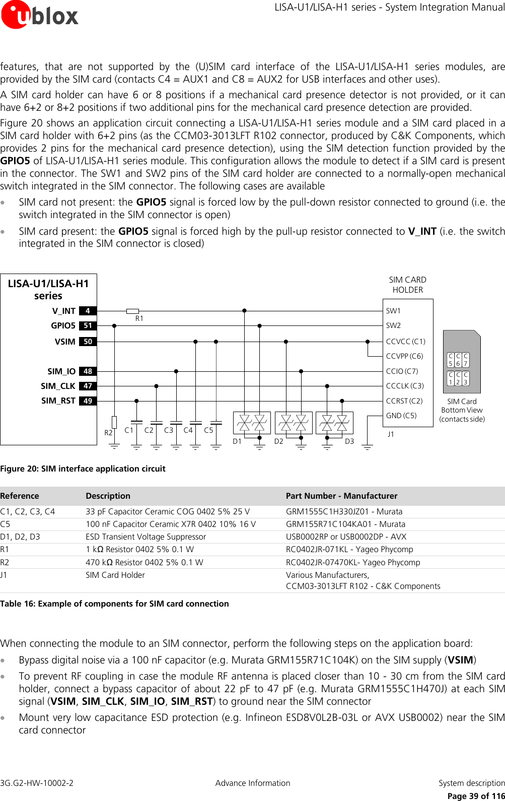
![LISA-U1/LISA-H1 series - System Integration Manual 3G.G2-HW-10002-2 Advance Information System description Page 13 of 116 Function Pin No I/O Description Remarks USB_D- 27 I/O USB Data Line D- 90 Ω nominal differential impedance Pull-up or pull-down resistors and external series resistors as required by the USB 2.0 high-speed specification [7] are part of the USB pad driver and need not be provided externally. Provide access to the pin for FW update and debugging if the USB interface is not connected to the application processor. See section 1.9.3 System PWR_ON 19 I Power-on input PWR_ON pin has high input impedance. Do not keep floating in noisy environment: external pull-up required. See section 1.6.1 RESET_N 22 I External reset input Internal 10 kΩ pull-up to V_BCKP (2.3 V). See section 1.6.3 Audio (LISA-U120, LISA-U130) I2S_CLK 43 O I2S clock Check device specifications to ensure compatibility to module supported modes. See section 1.11.2. I2S_RXD 44 I I2S receive data Internal active pull-up to V_INT (1.8 V) enabled. Check device specifications to ensure compatibility to module supported modes. See section 1.11.2. I2S_TXD 42 O I2S transmit data Check device specifications to ensure compatibility to module supported modes. See section 1.11.2. I2S_WA 41 O I2S word alignment Check device specifications to ensure compatibility to module supported modes. See section 1.11.2. MIC_N 39 I Differential analog audio input (negative) Differential analog input shared for all analog path modes: handset, headset, hands-free mode. Internal DC blocking capacitor. See section 1.11.1 MIC_P 40 I Differential analog audio input (positive) Differential analog input shared for all analog path modes: handset, headset, hands-free mode. Internal DC blocking capacitor. See section 1.11.1 SPK_P 53 O Differential analog audio output (positive) Differential analog audio output shared for all analog path modes: earpiece, headset and loudspeaker mode. See section 1.11.1 SPK_N 54 O Differential analog audio output (negative) Differential analog audio output shared for all analog path modes: earpiece, headset and loudspeaker mode. See section 1.11.1 Reserved RSVD 5 N/A RESERVED pin This pin must be connected to ground RSVD 52 N/A RESERVED pin Do not connect RSVD 74 N/A RESERVED pin Do not connect Reserved (LISA-U100, LISA-U110, LISA-H100, LISA-H110) RSVD 43 N/A RESERVED pin Do not connect RSVD 44 N/A RESERVED pin Do not connect RSVD 42 N/A RESERVED pin Do not connect RSVD 41 N/A RESERVED pin Do not connect RSVD 39 N/A RESERVED pin Do not connect RSVD 40 N/A RESERVED pin Do not connect RSVD 53 N/A RESERVED pin Do not connect RSVD 54 N/A RESERVED pin Do not connect Table 1: LISA-U1/LISA-H1 series modules pin-out](https://usermanual.wiki/u-blox/LISAU120/User-Guide-1470694-Page-13.png)
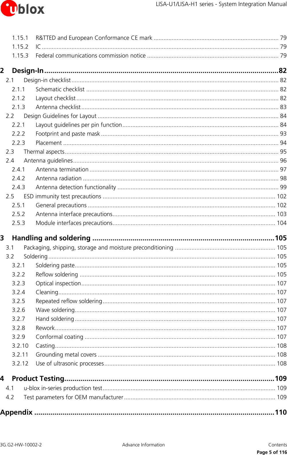
![LISA-U1/LISA-H1 series - System Integration Manual 3G.G2-HW-10002-2 Advance Information System description Page 14 of 116 1.4 Operating modes LISA-U1/LISA-H1 series modules include several operating modes, each have different active features and interfaces. Table 2 summarizes the various operating modes and provides general guidelines for operation. Operating Mode Description Features / Remarks Transition condition General Status: Power-down Not-Powered Mode VCC supply not present or below operating range. Microprocessor switched off (not operating). RTC only operates if supplied through V_BCKP pin. Module is switched off. Application interfaces are not accessible. Internal RTC timer operates only if a valid voltage is applied to V_BCKP pin. Module cannot be switched on by a falling edge provided on the PWR_ON input, or by a preset RTC alarm or by a rising edge provided on the RESET_N input. Power-Off Mode VCC supply within operating range. Microprocessor switched off (not operating). Only RTC runs. Module is switched off: normal shutdown after sending the AT+CPWROFF command (refer to u-blox AT Commands Manual [2]). Application interfaces are not accessible. Only the internal RTC timer in operation. Module can be switched on by a falling edge on the PWR_ON input, or by a rising edge on the RESET_N input, or by a preset RTC alarm. General Status: Normal Operation Idle-Mode Microprocessor runs with 32 kHz as reference oscillator. Module does not accept data signals from an external device. If power saving is enabled, the module automatically enters idle mode whenever possible. Application interfaces are disabled. If hardware flow control is enabled, the CTS line indicates that the module is in active mode and the UART interface is enabled: the line is driven in the OFF state when the module is not prepared to accept data by the UART interface. If hardware flow control is disabled, the CTS line is fixed to ON state. Module by default is not set to automatically enter idle mode whenever possible, unless power saving configuration is enabled by appropriate AT command (refer to u-blox AT Commands Manual [2], AT+UPSV). If the module is registered with the network and power saving is enabled, it automatically enters idle mode and periodically wakes up to active mode to monitor the paging channel for the paging block reception according to network indication. If module is not registered with the network and power saving is enabled, it automatically enters idle mode and periodically wakes up to monitor external activity. Module wakes up from idle mode to active mode if a voice or data call incoming. Module wakes up from idle mode to active mode if an RTC alarm occurs. Module wakes up from idle mode to active mode when data is received on UART interface (refer to 1.9.2). Module wakes up from idle mode to active mode when the RTS input line is set to the ON state by the DTE if the AT+UPSV=2 command is sent to the module (refer to 1.9.2). Module wakes up from idle mode to active mode at USB detection, applying 5 V (typ.) to the VUSB_DET pin. Module wakes up from idle mode to active mode when the connected USB host forces a remote wakeup of the module as USB device (refer to 1.9.3). Module wakes up from idle mode to active mode when the connected SPI master indicates to the module that it is ready to transmit or receive, by the IPC SPI_MRDY signal (refer to 1.9.4).](https://usermanual.wiki/u-blox/LISAU120/User-Guide-1470694-Page-14.png)
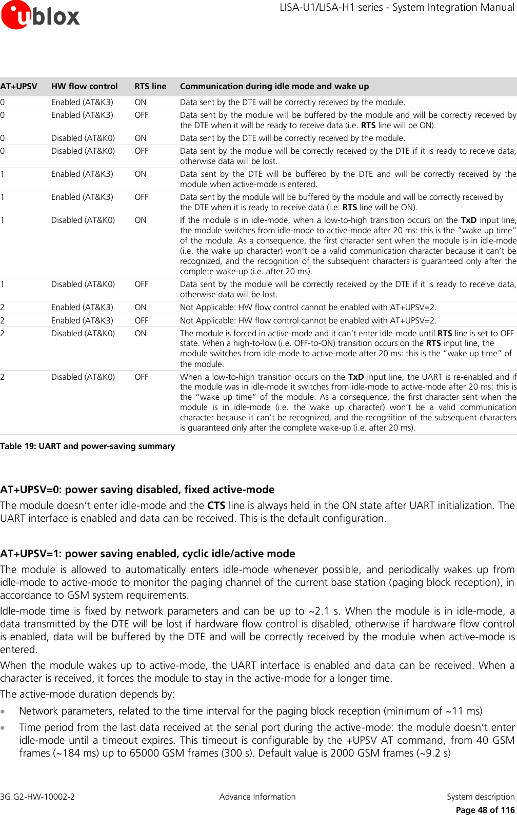
![LISA-U1/LISA-H1 series - System Integration Manual 3G.G2-HW-10002-2 Advance Information System description Page 15 of 116 Operating Mode Description Features / Remarks Transition condition Active-Mode Microprocessor runs with 26 MHz as reference oscillator. The module is prepared to accept data signals from an external device. Module is switched on and is fully active. Power saving is not enabled by default: it can be enabled by the AT+UPSV command (see u-blox AT Commands Manual [2]) The application interfaces are enabled. If power saving is enabled, the module automatically enters idle mode whenever possible (refer to u-blox AT Commands Manual [2], AT+UPSV). Connected-Mode Voice or data call enabled. Microprocessor runs with 26 MHz as reference oscillator. The module is prepared to accept data signals from an external device. The module is switched on and a voice call or a data call (2G/3G) is in progress. Module is fully active. The application interfaces are enabled. When call terminates, the module returns to the last operating state (Idle or Active). Table 2: Module operating modes summary Transition between the different modes is described in Figure 3. Switch ON:•Apply VCCIf power saving is enabled and there is no activity for a defined time intervalAny wake up event described in the module operating modes summary table aboveAT+CPWROFF(no HW pin)Incoming/outgoing call or other dedicated device network communicationCall terminated, communication droppedRemove VCCSwitch ON:•PWR_ON•RESET_N•RTC AlarmNot poweredPower offActiveConnected Idle Figure 3: Operating modes transition](https://usermanual.wiki/u-blox/LISAU120/User-Guide-1470694-Page-15.png)
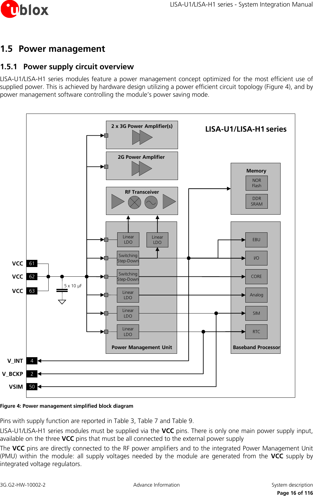
![LISA-U1/LISA-H1 series - System Integration Manual 3G.G2-HW-10002-2 Advance Information System description Page 17 of 116 V_BCKP is the Real Time Clock (RTC) supply. When the VCC voltage is within the valid operating range, the internal PMU supplies the Real Time Clock and the same supply voltage will be available to the V_BCKP pin. If the VCC voltage is under the minimum operating limit (for example, during not powered mode), the Real Time Clock can be externally supplied via the V_BCKP pin (see section 1.5.4). When a 1.8 V or a 3 V SIM card type is connected, LISA-U1/LISA-H1 series modules automatically supply the SIM card via the VSIM pin. Activation and deactivation of the SIM interface with automatic voltage switch from 1.8 to 3 V is implemented, in accordance to the ISO-IEC 7816-3 specifications. The same voltage domain used internally to supply the digital interfaces is also available on the V_INT pin, to allow more economical and efficient integration of the LISA-U1/LISA-H1 series modules in the final application. The integrated Power Management Unit also provides the control state machine for system start up and system reset control. 1.5.2 Module supply (VCC) The LISA-U1/LISA-H1 series modules must be supplied through the VCC pins by a DC power supply. Voltages must be stable: during operation, the current drawn from VCC can vary by some orders of magnitude, especially due to surging consumption profile of the GSM system (described in the section 1.5.3). It is important that the system power supply circuit is able to support peak power (refer to LISA-U1/LISA-H1 series Data Sheet [1] for specification). Name Description Remarks VCC Module power supply input VCC pins are internally connected, but all the available pads must be connected to the external supply in order to minimize the power loss due to series resistance. Clean and stable supply is required: low ripple and low voltage drop must be guaranteed. Voltage provided must always be above the minimum limit of the operating range. Consider that during a GSM call there are large current spikes in connected mode. GND Ground GND pins are internally connected but a good (low impedance) external ground can improve RF performance: all available pads must be connected to ground. Table 3: Module supply pins VCC pins ESD rating is 1 kV (contact discharge). A higher protection level can be required if the line is externally accessible on the application board. A higher protection level can be achieved by mounting an ESD protection (e.g. EPCOS CA05P4S14THSG varistor array) on the line connected to this pin. The voltage provided to the VCC pins must be within the normal operating range limits as specified in the LISA-U1/LISA-H1 series Data Sheet [1]. Complete functionality of the module is only guaranteed within the specified minimum and maximum VCC voltage operating range. Ensure that the input voltage at the VCC pins never drops below the minimum limit of the operating range when the module is switched on. This is the case even during a GSM transmit burst, where the current consumption can rise up to minimum peaks of 2.5 A in case of a mismatched antenna load. Operation above the operating range maximum limit is not recommended and extended exposure beyond it may affect device reliability.](https://usermanual.wiki/u-blox/LISAU120/User-Guide-1470694-Page-17.png)
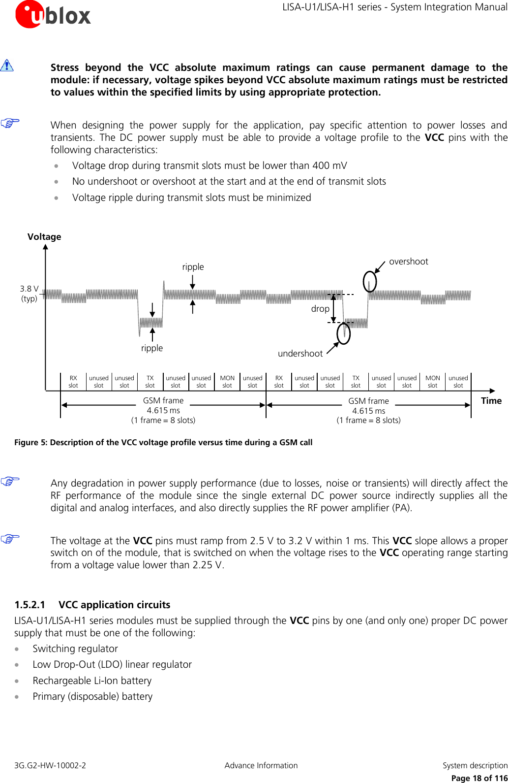

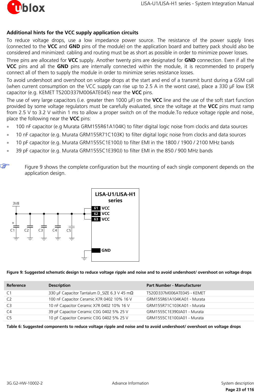
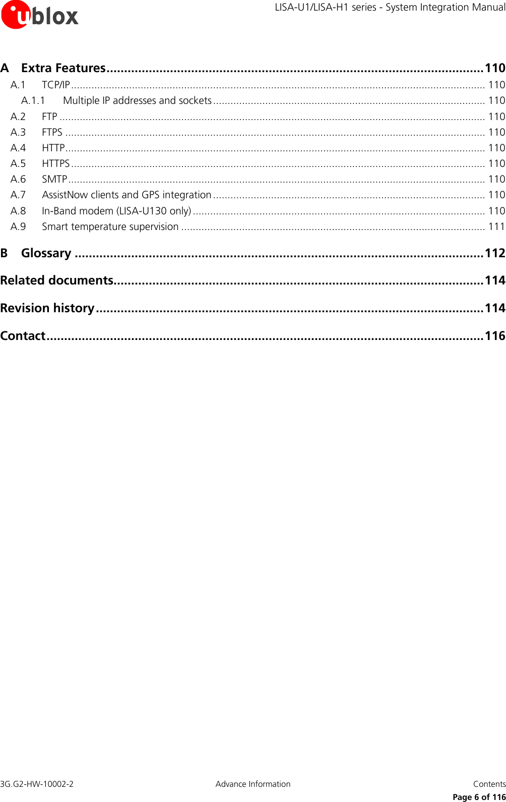
![LISA-U1/LISA-H1 series - System Integration Manual 3G.G2-HW-10002-2 Advance Information System description Page 24 of 116 1.5.3 Current consumption profiles During operation, the current drawn by the LISA-U1/LISA-H1 series modules through the VCC pins can vary by several orders of magnitude. This ranges from the high peak of current consumption during GSM transmitting bursts at maximum power level in 2G connected mode, to continuous high current drawn in UMTS connected mode, to the low current consumption during power saving in idle mode. 1.5.3.1 2G connected mode When a GSM call is established, the VCC consumption is determined by the current consumption profile typical of the GSM transmitting and receiving bursts. The current consumption peak during a transmission slot is strictly dependent on the transmitted power, which is regulated by the network. If the module is transmitting in GSM talk mode in the GSM 850 or in the E-GSM 900 band and at the maximum RF power control level (approximately 2 W or 33 dBm in the allocated transmit slot/burst) the current consumption can reach up to 2500 mA (with a highly unmatched antenna) for 576.9 µs (width of the transmit slot/burst) with a periodicity of 4.615 ms (width of 1 frame = 8 slots/burst), so with a 1/8 duty cycle according to GSM TDMA (Time Division Multiple Access). During a GSM call, current consumption is in the order of 100-200 mA in receiving or in monitor bursts and is about 30-50 mA in the inactive unused bursts (low current period). The more relevant contribution to determine the average current consumption is set by the transmitted power in the transmit slot. An example of current consumption profile of the data module in GSM talk mode is shown in Figure 10. Time [ms]RX slotunused slotunused slotTX slotunused slotunused slotMON slotunused slotRX slotunused slotunused slotTX slotunused slotunused slotMON slotunused slotGSM frame 4.615 ms (1 frame = 8 slots)Current [A]200 mA ~170 mA2500 mAPeak current depends on TX powerGSM frame 4.615 ms (1 frame = 8 slots)1.51.00.50.02.52.0~170 mA ~40 mA Figure 10: VCC current consumption profile versus time during a GSM call (1 TX slot, 1 RX slot), with VCC=3.8 V When a GPRS connection is established there is a different VCC current consumption profile also determined by the transmitting and receiving bursts. In contrast to a GSM call, during a GPRS connection more than one slot can be used to transmit and/or more than one slot can be used to receive. The transmitted power depends on network conditions, which set the peak current consumption, but following the GPRS specifications the maximum transmitted RF power is reduced if more than one slot is used to transmit, so the maximum peak of current consumption is not as high as can be in case of a GSM call. If the module transmits in GPRS class 12 connected mode in the GSM 850 or in the E-GSM 900 band at the maximum power control level (27 dBm typical transmitted power in the transmit slot/burst), the current consumption can reach up to 1400 mA (with unmatched antenna). This happens for 2.307 ms (width of the 4 transmit slots/bursts) with a periodicity of 4.615 ms (width of 1 frame = 8 slots/bursts), so with a 1/2 duty cycle, according to GSM TDMA.](https://usermanual.wiki/u-blox/LISAU120/User-Guide-1470694-Page-24.png)
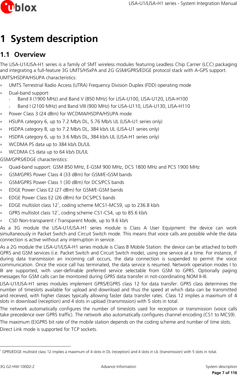
![LISA-U1/LISA-H1 series - System Integration Manual 3G.G2-HW-10002-2 Advance Information System description Page 25 of 116 Figure 11 reports the current consumption profiles in GPRS mode with 4 slots used to transmit. Time [ms]RX slotunused slotTX slotTX slotTX slotTX slotMON slotunused slotRX slotunused slotTX slotTX slotTX slotTX slotMON slotunused slotGSM frame 4.615 ms (1 frame = 8 slots)Current [A]200mA ~170mAPeak current depends on TX power~170mAGSM frame 4.615 ms (1 frame = 8 slots)1.51.00.50.02.52.0~40mA1400 mA Figure 11: VCC current consumption profile versus time during a GPRS/EDGE connection (4TX slots, 1 RX slot), with VCC=3.8 V In case of EDGE connections the VCC current consumption profile is very similar to the GPRS current profile, so the image shown in Figure 11 is valid for EDGE as well. 1.5.3.2 3G connected mode During a 3G connection, the module can transmit and receive continuously due to the Frequency Division Duplex (FDD) mode of operation with the Wideband Code Division Multiple Access (WCDMA). The current consumption depends again on output RF power, which is always regulated by network commands. These power control commands are logically divided into a slot of 666 µs, thus the rate of power change can reach a maximum rate of 1.5 kHz. There are no high current peaks as in the 2G connection, since transmission and reception are continuously enabled due to FDD WCDMA implemented in the 3G that differs from the TDMA implemented in the 2G case. In the worst scenario, corresponding to a continuous transmission and reception at maximum output power (approximately 250 mW or 24 dBm), the current drawn by the module at the VCC pins is in the order of continuous 600-700 mA. Even at lowest output RF power (approximately 0.01 µW or -50 dBm), the current still remains in the order of 200 mA due to module baseband processing and transceiver activity. An example of current consumption profile of the data module in UMTS continuous transmission mode is shown in Figure 12.](https://usermanual.wiki/u-blox/LISAU120/User-Guide-1470694-Page-25.png)
![LISA-U1/LISA-H1 series - System Integration Manual 3G.G2-HW-10002-2 Advance Information System description Page 26 of 116 Time [ms]3G frame 10 ms (1 frame = 15 slots)Current [mA]170 mADepends on TX power1 slot 666 µs670 mA3002001000500400600700 Figure 12: VCC current consumption profile versus time during a UMTS connection, with VCC=3.8 V When a packet data connection is established, the actual current profile depends on the amount of transmitted packets; there might be some periods of inactivity between allocated slots where current consumption drops about 100 mA. Alternatively, at higher data rates the transmitted power is likely to increase due to the higher quality signal required by the network to cope with enhanced data speed. 1.5.3.3 2G and 3G cyclic idle/active mode (power saving enabled) The power saving configuration is by default disabled, but it can be enabled using the appropriate AT command (refer to u-blox AT Commands Manual [2], AT+UPSV command). When the power saving is enabled, the module automatically enters idle-mode whenever possible. When power saving is enabled, the module is registered or attached to a network and a voice or data call is not enabled, the module automatically enters idle-mode whenever possible, but it must periodically monitor the paging channel of the current base station (paging block reception), in accordance to GSM system requirements. When the module monitors the paging channel, it wakes up to active mode, to enable the reception of paging block. In between, the module switches to idle-mode. This is known as GSM discontinuous reception (DRX). The module processor core is activated during the paging block reception, and automatically switches its reference clock frequency from 32 kHz to the 26 MHz used in active-mode. The time period between two paging block receptions is defined by the network (2G or 3G). This is the paging period parameter, fixed by the base station through broadcast channel sent to all users on the same serving cell. In case of 2G network, the time interval between two paging block receptions can be from 470.76 ms (width of 2 GSM multiframes = 2 x 51 GSM frames = 2 x 51 x 4.615 ms) up to 2118.42 ms (width of 9 GSM multiframes = 9 x 51 frames = 9 x 51 x 4.615 ms). In case of 3G network, the principle is similar but time interval changes from 640 ms (width of 26 x 3G frames = 64 x 10 ms = 640 ms) up to 5120 ms (width of 29 x 3G frames = 512 x 10 ms = 5120 ms). An example of a module current consumption profile is shown in Figure 13: the module is registered with the network (2G or 3G), automatically enters idle mode and periodically wakes up to active mode to monitor the paging channel for paging block reception.](https://usermanual.wiki/u-blox/LISAU120/User-Guide-1470694-Page-26.png)
![LISA-U1/LISA-H1 series - System Integration Manual 3G.G2-HW-10002-2 Advance Information System description Page 27 of 116 ~30 msIDLE MODE ACTIVE MODE IDLE MODE500-700 µA 8-10 mA 20-22 mA~150 mAActive Mode EnabledIdle Mode EnabledPLL EnabledRX+DSP Enabled500-700 µA~150 mA2G case: 0.44-2.09 s 3G case: 0.61-5.09 sIDLE MODE2G or 3G case: ~30 msACTIVE MODETime [s]Current [mA]150100500Time [ms]Current [mA]150100500 Figure 13: Description of VCC current consumption profile versus time when the module is registered with 2G or 3G networks: the module is in idle mode and periodically wakes up to active mode to monitor the paging channel for paging block reception 1.5.3.4 2G and 3G fixed active mode (power saving disabled) Power saving configuration is by default disabled, or it can be disabled using the appropriate AT command (refer to u-blox AT Commands Manual [2], AT+UPSV command). When power saving is disabled, the module doesn’t automatically enter idle-mode whenever possible: the module remains in active mode. The module processor core is activated during active-mode, and the 26 MHz reference clock frequency is used. An example of the current consumption profile of the data module when power saving is disabled is shown in Figure 14: the module is registered with the network, active-mode is maintained, and the receiver and the DSP are periodically activated to monitor the paging channel for paging block reception.](https://usermanual.wiki/u-blox/LISAU120/User-Guide-1470694-Page-27.png)
![LISA-U1/LISA-H1 series - System Integration Manual 3G.G2-HW-10002-2 Advance Information System description Page 28 of 116 ACTIVE MODE20-22 mA 20-22 mA~150 mARX+DSP Enabled20-22 mA~150 mA2G case: 0.47-2.12 s 3G case: 0.64-5.12 sPaging periodTime [s]Current [mA]150100500Time [ms]Current [mA]150100500 Figure 14: Description of the VCC current consumption profile versus time when power saving is disabled: active-mode is always held, and the receiver and the DSP are periodically activated to monitor the paging channel for paging block reception 1.5.4 RTC Supply (V_BCKP) The V_BCKP pin connects the supply for the Real Time Clock (RTC) and Power On / Reset internal logic. This supply domain is internally generated by a linear regulator integrated in the Power Management Unit. The output of this linear regulator is always enabled when the main voltage supply provided to the module through VCC is within the valid operating range, with the module switched-off or powered-on. Name Description Remarks V_BCKP Real Time Clock supply V_BCKP = 2.3 V (typical) generated by the module to supply Real Time Clock when VCC supply voltage is within valid operating range. Table 7: Real Time Clock supply pin The V_BCKP pin ESD rating is 1 kV (contact discharge). A higher protection level could be required if the line is externally accessible on the application board. A higher protection level can be achieved by mounting an ESD protection (e.g. EPCOS CA05P4S14THSG varistor array) on the line connected to this pin. The RTC provides the time reference (date and time) of the module, also in power off mode, when the V_BCKP voltage is within its valid range (specified in u-blox LISA-U1/LISA-H1 series Data Sheet [1]). The RTC timing is](https://usermanual.wiki/u-blox/LISAU120/User-Guide-1470694-Page-28.png)
![LISA-U1/LISA-H1 series - System Integration Manual 3G.G2-HW-10002-2 Advance Information System description Page 29 of 116 normally used to set the wake-up interval during idle-mode periods between network paging, but is able to provide programmable alarm functions by means of the internal 32.768 kHz clock. The RTC can be supplied from an external back-up battery through the V_BCKP, when the main voltage supply is not provided to the module through VCC. This lets the time reference (date and time) run even when the main supply is not provided to the module. Consider that the module cannot switch on if a valid voltage is not present on VCC even when the RTC is supplied through V_BCKP (meaning that VCC is mandatory to switch-on the module). The RTC has very low power consumption, but is highly temperature dependent. For example at 25°C and a V_BCKP voltage of 2.3 V the power consumption is approximately 2 µA, whereas at 70°C and an equal voltage the power consumption increases to 5-10 µA. The internal regulator for V_BCKP is optimized for low leakage current and very light loads. It is not recommended to use V_BCKP to supply external loads. If V_BCKP is left unconnected and the module main voltage supply is removed from VCC, the RTC is supplied from the 100 nF capacitor mounted inside the module. However, this capacitor is not able to provide a long buffering time: within few milliseconds the voltage on V_BCKP will go below the valid range (1 V min). At this time the internal RTC will stop counting and the date and time setting will be lost. This has no impact on wireless connectivity, as all the functionalities of the module do not rely on the date and time setting. Leave V_BCKP unconnected if the RTC is not required when the VCC supply is removed. The date and time will not be updated when VCC is disconnected. If VCC is always supplied, then the internal regulator is supplied from the main supply and there is no need for an external component on V_BCKP. If RTC is required to run for a time interval of T [s] at 25°C when VCC supply is removed, place a capacitor with a nominal capacitance of C [µF] at the V_BCKP pin. Choose the capacitor using the following formula: C [µF] = (Current_Consumption [µA] x T [s]) / Voltage_Drop [V] = 1.538 x T [s] The RTC current consumption is approximately 2 µA at 25°C, and the voltage drop is equal to 1.3 V (from the V_BCKP typical value of 2.3 V to the valid range minimum limit of 1.0 V). For example, a 100 µF capacitor (such as the Murata GRM43SR60J107M) can be placed at V_BCKP to provide a long buffering time. This capacitor will hold V_BCKP voltage within its valid range for around 50 s at 25°C, after the VCC supply is removed. If a very long buffering time is required, a 70 mF super-capacitor (e.g. Seiko Instruments XH414H-IV01E) can be placed at V_BCKP, with a 4.7 k series resistor to hold the V_BCKP voltage within its valid range for approximately 10 hours at 25°C, after the VCC supply is removed. The purpose of the series resistor is to limit the capacitor charging current due to the large capacitor specifications, and also to let a fast rise time of the voltage value at the V_BCKP pin after VCC supply has been provided. These capacitors will allow the time reference to run during battery disconnection. LISA-U1/LISA-H1 seriesC1(a)2V_BCKPR2LISA-U1/LISA-H1 seriesC2(superCap)(b)2V_BCKPD3LISA-U1/LISA-H1 series2.3 V(c)2V_BCKP Figure 15: Real time clock supply (V_BCKP) application circuits : (a) using a 100 µF capacitor to let the RTC run for ~50 s at 25°C; (b) using a 70 mF capacitor to let the RTC run for ~10 hours at 25°C when the VCC supply is removed; (c) using non-rechargeable battery](https://usermanual.wiki/u-blox/LISAU120/User-Guide-1470694-Page-29.png)
![LISA-U1/LISA-H1 series - System Integration Manual 3G.G2-HW-10002-2 Advance Information System description Page 30 of 116 Reference Description Part Number - Manufacturer C1 100 µF Tantalum Capacitor GRM43SR60J107M - Murata R2 4.7 kΩ Resistor 0402 5% 0.1 W RC0402JR-074K7L - Yageo Phycomp C2 70 mF Capacitor XH414H-IV01E - Seiko Instruments Table 8: Example of components for V_BCKP buffering If longer buffering time is required to allow the time reference to run during a disconnection of the VCC supply, then an external battery can be connected to V_BCKP pin. The battery should be able to provide a 2.3 V nominal voltage and must never exceed the maximum operating voltage for V_BCKP. The connection of the battery to V_BCKP should be done with a suitable series resistor for a rechargeable battery, or with an appropriate series diode for a non-rechargeable battery. The purpose of the series resistor is to limit the battery charging current due to the battery specifications, and also to allow a fast rise time of the voltage value at the V_BCKP pin after the VCC supply has been provided. The purpose of the series diode is to avoid a current flow from the module V_BCKP pin to the non-rechargeable battery. 1.5.5 Interface supply (V_INT) The same voltage domain used internally to supply the digital interfaces is also available on the V_INT pin. The internal regulator that generates the V_INT supply is a switching step down converter that is directly supplied from VCC. The voltage regulator output is set to 1.8 V (typical) when the module is switched on and is disabled when the module is switched off or when the RESET_N pin is forced the low level. The switching regulator operates in Pulse Width Modulation (PWM) for high output current mode but automatically switches to Pulse Frequency Modulation (PFM) at low output loads for greater efficiency, e.g. when the module is in idle mode between paging periods. Name Description Remarks V_INT Digital Interfaces supply output V_INT = 1.8V (typical) generated by the module when it is switched-on and the RESET_N (external reset input pin) is not forced to the low level. V_INT is the internal supply for digital interfaces. The user may draw limited current from this supply rail. Table 9: Interface supply pin The V_INT pin ESD rating is 1 kV (contact discharge). A higher protection level could be required if the line is externally accessible on the application board. A higher protection level can be achieved by mounting an ESD protection (e.g. EPCOS CA05P4S14THSG varistor array) on the line connected to this pin. Since it supplies internal digital circuits (see Figure 4), V_INT is not suited to directly supply any sensitive analog circuit: the voltage ripple can range from 15 mVpp during active mode (PWM), to 70 mVpp in idle mode (PFM). V_INT can be used to supply external digital circuits operating at the same voltage level as the digital interface pins, i.e. 1.8 V (typical). It is not recommended to supply analog circuitry without adequate filtering for digital noise. Don’t apply loads which might exceed the limit for maximum available current from V_INT supply, as this can cause malfunctions in internal circuitry supplies to the same domain. The detailed electrical characteristics are described in the LISA-U1/LISA-H1 series Data Sheet [1].](https://usermanual.wiki/u-blox/LISAU120/User-Guide-1470694-Page-30.png)
![LISA-U1/LISA-H1 series - System Integration Manual 3G.G2-HW-10002-2 Advance Information System description Page 31 of 116 V_INT can only be used as an output; don’t connect any external regulator on V_INT. If not used, this pin should be left unconnected. The V_INT digital interfaces supply output is mainly used to: Pull-up DDC (I2C) interface signals (see section 1.10 for more details) Pull-up SIM detection signal (see section 1.8 for more details) Indicate when the module is switched on and the RESET_N (external reset input pin) is not forced to the low level 1.6 System functions 1.6.1 Module power on The module power on sequence is initiated in one of 3 ways: Rising edge on the VCC pin to a valid voltage for module supply Falling edge on the PWR_ON pin Rising edge on the RESET_N pin RTC alarm Name Description Remarks PWR_ON Power on input PWR_ON pin has high input impedance. Do not keep floating in noisy environment: external pull-up required. Table 10: Power on pin The PWR_ON pin ESD rating is 1 kV (contact discharge). A higher protection level could be required if the line is externally accessible on the application board. A higher protection level can be achieved mounting an ESD protection (e.g. EPCOS CA05P4S14THSG varistor array) on the line connected to this pin. 1.6.1.1 Rising edge on VCC When a supply is connected to VCC pins, the module supply supervision circuit controls the subsequent activation of the power up state machines: the module is switched on when the voltage rises up to the VCC operating range minimum limit (3.4 V) starting from a voltage value lower than 2.25 V (See LISA-U1/LISA-H1 series Data Sheet [1]). The voltage at the VCC pins must ramp from 2.5 V to 3.2 V within 1 ms to switch on the module. 1.6.1.2 Falling edge on PWR_ON The module power on sequence starts when a falling edge is forced on the PWR_ON input pin. After applying a falling edge, it is suggested to hold a low level on the PWR_ON signal for at least 5 ms to properly switch on the module. The electrical characteristics of the PWR_ON input pin are different from the other digital I/O interfaces: the high and the low logic levels have different operating ranges and the pin is tolerant to voltages up to the battery voltage. The detailed electrical characteristics are described in the LISA-U1/LISA-H1 series Data Sheet [1].](https://usermanual.wiki/u-blox/LISAU120/User-Guide-1470694-Page-31.png)
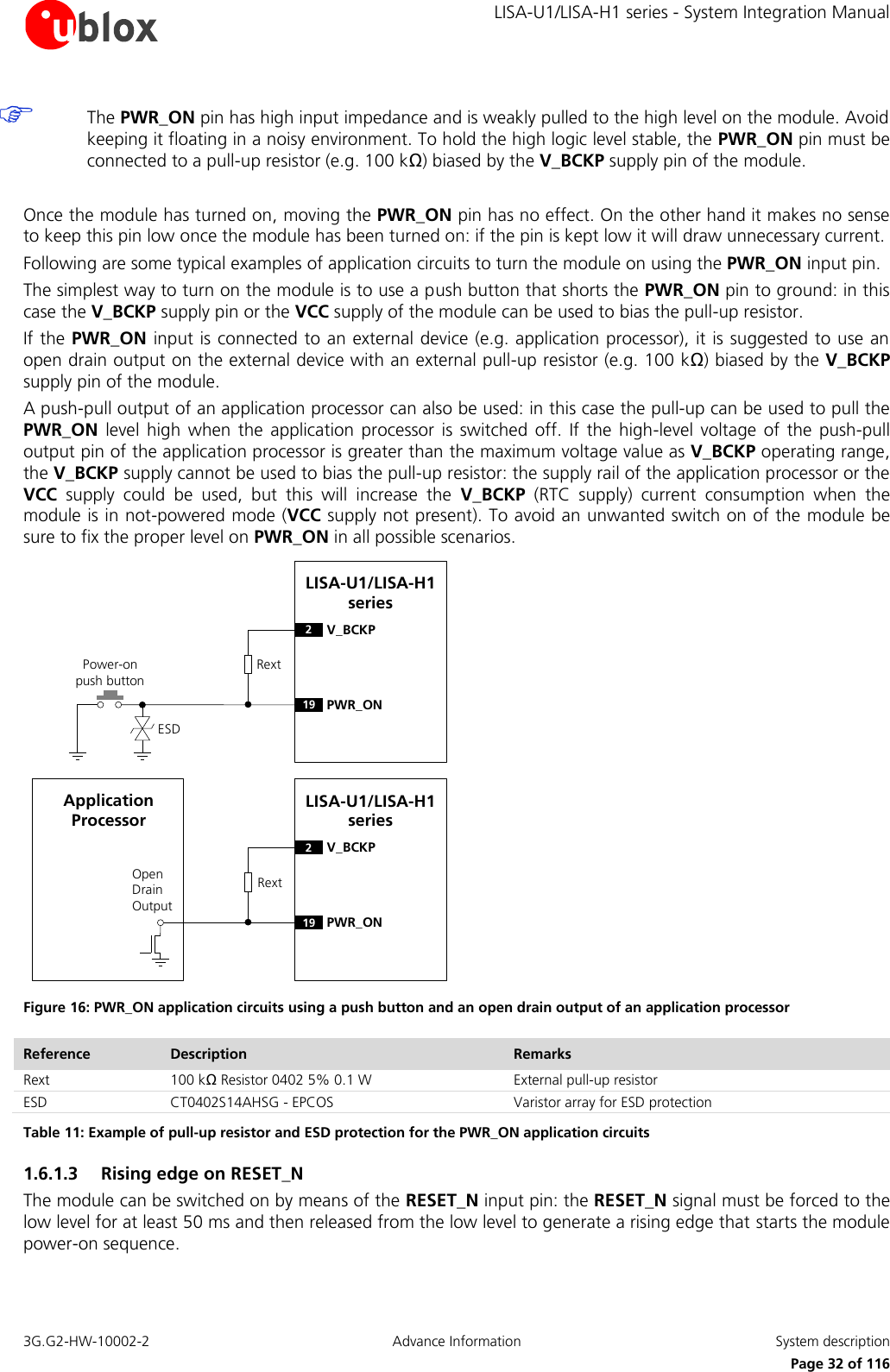
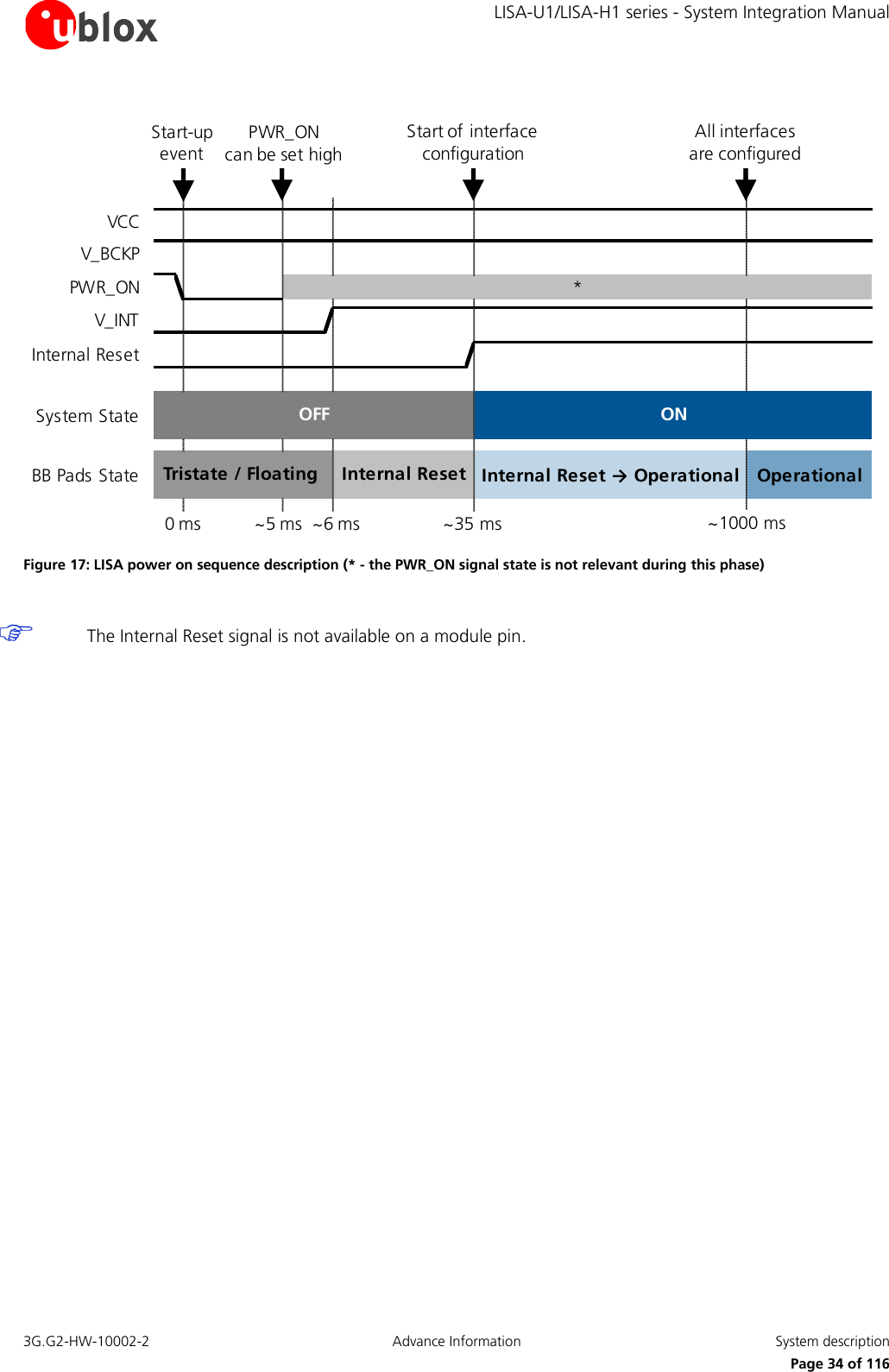
![LISA-U1/LISA-H1 series - System Integration Manual 3G.G2-HW-10002-2 Advance Information System description Page 33 of 116 The RESET_N input pin can also be used to perform an “external” or “hardware” reset of the module, as described in the section 1.6.3. The electrical characteristics of RESET_N are different from the other digital I/O interfaces. The detailed electrical characteristics are described in the LISA-U1/LISA-H1 series Data Sheet [1]. RESET_N is pulled high to V_BCKP by an integrated pull-up resistor also when the module is in power off mode. Therefore an external pull-up should not be required on the application board. The simplest way to switch on the module by means of the RESET_N input pin is to use a push button that shorts the RESET_N pin to ground: the module will be switched on at the release of the push button, since the RESET_N will be forced to the high level by the integrated pull-up resistor, generating a rising edge. If RESET_N is connected to an external device (e.g. an application processor on an application board) an open drain output can be directly connected without any external pull-up. A push-pull output can be used too: in this case make sure that the high level voltage of the push-pull circuit is below the maximum voltage value of the V_BCKP operating range. Make sure to fix the proper level on RESET_N in all possible scenarios, to avoid unwanted switch-on or reset of the module. Some typical examples of application circuits using the RESET_N input pin are described in the section 1.6.3. 1.6.1.4 Real Time Clock (RTC) alarm If a voltage within the operating range is maintained at the VCC pin, the module can be switched on by the RTC alarm when the RTC system reaches a pre-programmed scheduled time. The RTC system will then initiate the boot sequence by instructing the Power Management Unit to turn on power. Also included in this setup is an interrupt signal from the RTC block to indicate to the baseband processor that an RTC event has occurred. 1.6.1.5 Additional considerations The module is switched on when the voltage rises up to the VCC operating range: the first time that the module is used, it is switched on in this way. Then, the proper way to switch off the module is by means of the AT+CPWROFF command. When the module is in power-off mode, i.e. the AT+CPWROFF command has been sent and a voltage value within the operating range limits is still provided to the VCC pin, the digital input-output pads of the baseband chipset (i.e. all the digital pins of the module) are locked in tri-state (i.e. floating). The power down tri-state function isolates the module pins from its environment, when no proper operation of the outputs can be guaranteed. The module can be switched on from power-off mode by forcing a proper start-up event (i.e. a falling edge on the PWR_ON pin, or an RTC alarm). After the detection of a start-up event, all the digital pins of the module are held in tri-state until all the internal LDO voltage regulators are turned on in a defined power-on sequence. Then, as described in Figure 17, the baseband core is still held in reset state for a time interval: the internal reset signal (which is not available on a module pin) is still low and any signal from the module digital interfaces is held in reset state. The reset state of all the digital pins is reported in the pin description table of the LISA-U1/LISA-H1 series Data Sheet [1]. When the internal signal is released, the configuration of the module interfaces starts: during this phase any digital pin is set in a proper sequence from the reset state to the default operational configuration. Finally, the module is fully ready to operate when all interfaces are configured.](https://usermanual.wiki/u-blox/LISAU120/User-Guide-1470694-Page-33.png)
![LISA-U1/LISA-H1 series - System Integration Manual 3G.G2-HW-10002-2 Advance Information System description Page 35 of 116 1.6.2 Module power off The correct way to switch off LISA-U1/LISA-H1 series modules is by means of +CPWROFF AT command (more details in u-blox AT Commands Manual [2]): in this way the current parameter settings are saved in the module’s non-volatile memory and a proper network detach is performed. An under-voltage shutdown will be done if the VCC supply is removed, but in this case the current parameter settings are not saved in the module’s non-volatile memory and a proper network detach cannot be performed. The power off sequence is described in Figure 18. When the +CPWROFF AT command is sent, the module starts the switch-off routine replying OK on the AT interface: during this phase, the current parameter settings are saved in the module’s non-volatile memory, a network detach is performed and all module interfaces are disabled (i.e. the digital pins are locked in tri-state by the module). Since the time to perform a network detach depends on the network settings, the duration of this phase can differ from the typical value reported in the following figure. At the end of the switch-off routine, all the digital pins are locked in tri-state by the module and all the internal LDO voltage regulators except the RTC supply (V_BCKP) are turned off in a defined power off sequence. The module remains in power off mode as long as a switch on event doesn’t occur (i.e. a falling edge on the PWR_ON pin or an RTC alarm), and enters not-powered mode if the supply is removed from the VCC pin. VCCV_BCKPPWR_ON *V_INTInternal ResetSystem StateBB Pads State OperationalOFFTristate / Floating ONOperational → Tristate / FloatingAT+CPWROFFsent to the module0 ms~50 ms~400 msOKreplied by the module Figure 18: LISA Power off sequence description (* - the PWR_ON signal state is not relevant during this phase) The Internal Reset signal is not available on a module pin. Tristated pins are always subject to floating caused by noise: to prevent unwanted effects, fix them with proper pull-up or pull down resistors to stable voltage rails to fix their level when the module is in Power down state.](https://usermanual.wiki/u-blox/LISAU120/User-Guide-1470694-Page-35.png)
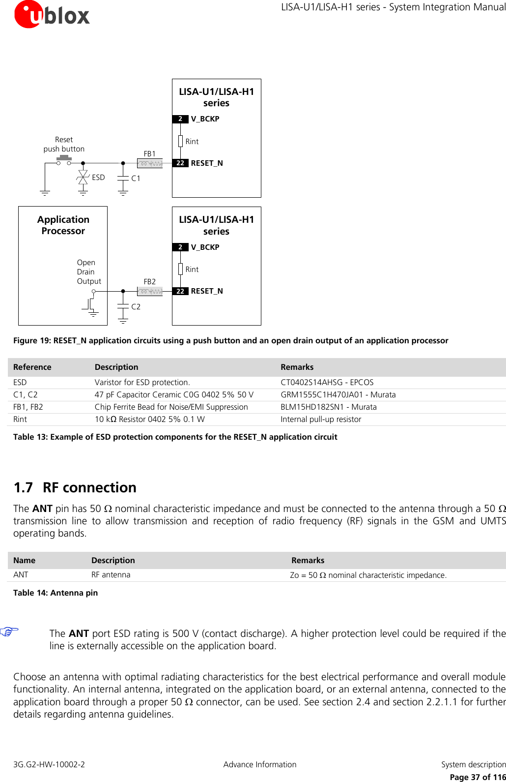
![LISA-U1/LISA-H1 series - System Integration Manual 3G.G2-HW-10002-2 Advance Information System description Page 36 of 116 1.6.3 Module reset The module reset can be performed in one of 2 ways: Forcing a low level on the RESET_N pin, causing an “external” or “hardware” reset Via AT command, causing an “internal” or “software” reset LISA-U1/LISA-H1 series modules can be reset using the RESET_N pin: when the RESET_N pin is forced low for at least 50 ms, an “external” or “hardware” reset is performed. This causes an asynchronous reset of the entire module, including the integrated Power Management Unit, except for the RTC internal block: the V_INT interfaces supply is switched off and all the digital pins are tri-stated, but the V_BCKP supply and the RTC block are enabled. Forcing an “external” or “hardware” reset, the current parameter settings are not saved in the module’s non-volatile memory and a proper network detach is not performed. LISA-U1/LISA-H1 series modules can also be reset by means of the AT+CFUN command (more details in u-blox AT Commands Manual [2]): in this case an “internal” or “software” reset is performed, causing an asynchronous reset of the baseband processor, excluding the integrated Power Management Unit and the RTC internal block: the V_INT interfaces supply is enabled and each digital pin is set in its internal reset state (reported in the pin description table in the LISA-U1/LISA-H1 series Data Sheet [1]), the V_BCKP supply and the RTC block are enabled. Forcing an “internal” or “software” reset, the current parameter settings are saved in the module’s non-volatile memory and a proper network detach is performed. When RESET_N is released from the low level, the module automatically starts its power on sequence from the reset state. The same procedure is followed for the module reset via AT command after having performed the network detach and the parameter saving in non-volatile memory. The internal reset state of all digital pins is reported in the pin description table in LISA-U1/LISA-H1 series Data Sheet [1]. Name Description Remarks RESET_N External reset input Internal 10 k pull-up to V_BCKP Table 12: Reset pin The RESET_N pin ESD rating is 1 kV (contact discharge). A higher protection level could be required if the line is externally accessible on the application board. A higher protection level can be achieved mounting an ESD protection (e.g. EPCOS CA05P4S14THSG varistor array) on the line connected to this pin. For more details about the general precautions for ESD immunity about RESET_N pin please refer to chapter 2.5.1. The electrical characteristics of RESET_N are different from the other digital I/O interfaces. The detailed electrical characteristics are described in the LISA-U1/LISA-H1 series Data Sheet [1]. RESET_N is pulled high by an integrated 10 k pull-up resistor to V_BCKP. Therefore an external pull-up is not required on the application board. Following are some typical examples of application circuits using the RESET_N input pin. The simplest way to reset the module is to use a push button that shorts the RESET_N pin to ground. If RESET_N is connected to an external device (e.g. an application processor on an application board) an open drain output can be directly connected without any external pull-up. A push-pull output can be used too: in this case make sure that the high level voltage of the push-pull circuit is below the maximum voltage value of the V_BCKP operating range. To avoid unwanted reset of the module make sure to fix the proper level on RESET_N in all possible scenarios. As ESD immunity test precaution, a 47 pF bypass capacitor (e.g. Murata GRM1555C1H470JA01) and a series ferrite bead (e.g. Murata BLM15HD182SN1) must be added on the RESET_N line pin to avoid a module reset caused by an electrostatic discharge applied to the application board (for more details, refer to chapter 2.5.1).](https://usermanual.wiki/u-blox/LISAU120/User-Guide-1470694-Page-36.png)
![LISA-U1/LISA-H1 series - System Integration Manual 3G.G2-HW-10002-2 Advance Information System description Page 41 of 116 1.9 Serial communication LISA-U1/LISA-H1 series modules provide AT command interface, Packet-Switched / Circuit-Switched Data communication on the following serial communication interfaces: One asynchronous serial interface (UART) that provides complete RS-232 functionality conforming to ITU-T V.24 Recommendation [3], with limited data rate. The UART interface can be used for firmware upgrade One Inter Processor Communication (IPC) interface that includes a synchronous SPI-compatible interface, with maximum data rate of 20 Mb/s One high-speed USB 2.0 compliant interface, with maximum data rate of 480 Mb/s. The single USB interface implements 6 logical devices. Each device is a USB communications device class (or USB CDC), that is a composite Universal Serial Bus device class. The USB interface can be used for firmware upgrade The LISA-U1/LISA-H1 series modules are designed to operate as an HSPA wireless modem, which represents the data circuit-terminating equipment (DCE) as described by the ITU-T V.24 Recommendation [3]. A customer application processor connected to the module through one of the interfaces represents the data terminal equipment (DTE). All the interfaces listed above are controlled and operated with: AT commands according to 3GPP TS 27.007 [4] AT commands according to 3GPP TS 27.005 [5] AT commands according to 3GPP TS 27.010 [6] u-blox AT commands For the complete list of supported AT commands and their syntax refer to the u-blox AT Commands Manual [2]. The following serial communication interfaces can be used for firmware upgrade: The UART interface, using the RxD and TxD lines only The USB interface, using all the lines provided (VUSB_DET, USB_D+ and USB_D-) To directly enable PC (or similar) connection to the module for firmware upgrade, provide direct access on the application board to the VUSB_DET, USB_D+ and USB_D- lines of the module (or to the RxD and TxD lines). Also provide access to the PWR_ON or the RESET_N pins, or enable the DC supply connected to the VCC pin to start the module firmware upgrade (see Firmware Update Application Note [14]). The following sub-chapters describe the serial interfaces configuration and provide a detailed description of each interface for the application circuits. 1.9.1 Serial interfaces configuration UART, USB and SPI/IPC serial interfaces are available as AT command interface and for Packet-Switched / Circuit-Switched Data communication. The serial interfaces are configured as described in Table 17 (for information about further settings, please refer to the u-blox AT Commands Manual [2]).](https://usermanual.wiki/u-blox/LISAU120/User-Guide-1470694-Page-41.png)
![LISA-U1/LISA-H1 series - System Integration Manual 3G.G2-HW-10002-2 Advance Information System description Page 42 of 116 Interface AT Settings Comments UART interface Enabled Multiplexing mode can be enabled by AT+CMUX command providing following channels: Channel 0: control channel Channel 1 – 5: AT commands /data connection Channel 6: GPS tunneling AT+IPR=115200 Baud rate: 115200 b/s AT+ICF=0,0 Frame format: 8 bits, no parity, 1 stop bit AT&K3 HW flow control enabled AT&S1 DSR line set ON in data mode and set OFF in command mode AT&D1 Upon an ON-to-OFF transition of DTR, the DCE enters online command state and issues an OK result code AT&C1 Circuit 109 changes in accordance with the Carrier detect status; ON if the Carrier is detected, OFF otherwise USB interface Enabled 6 CDCs are available, configured as described in the following list: USB1: AT commands / data connection USB2: AT commands / data connection USB3: AT commands / data connection USB4: GPS tunneling dedicated port USB5: 2G trace dedicated port USB6: 3G trace dedicated port AT&K3 HW flow control enabled AT&S1 DSR line set ON in data mode and set OFF in command mode AT&D1 Upon an ON-to-OFF transition of DTR, the DCE enters online command state and issues an OK result code AT&C1 Circuit 109 changes in accordance with the Carrier detect status; ON if the Carrier is detected, OFF otherwise SPI interface Enabled Multiplexing mode can be enabled by AT+CMUX command providing following channels: Channel 0: control channel Channel 1 – 5: AT commands /data connection Channel 6: GPS tunneling AT&K3 HW flow control enabled AT&S1 DSR line set ON in data mode and set OFF in command mode AT&D1 Upon an ON-to-OFF transition of DTR, the DCE enters online command state and issues an OK result code AT&C1 Circuit 109 changes in accordance with the Carrier detect status; ON if the Carrier is detected, OFF otherwise Table 17: Default serial interfaces configuration 1.9.2 Asynchronous serial interface (UART) The UART interface is a 9-wire unbalanced asynchronous serial interface that provides AT commands interface, PSD and CSD data communication, firmware upgrade. UART interface provides RS-232 functionality conforming to the ITU-T V.24 Recommendation (more details available in ITU Recommendation [3]), with CMOS compatible signal levels: 0 V for low data bit or ON state, and 1.8 V for high data bit or OFF state. Two different external voltage translators (Maxim MAX3237E and On Semiconductor NLSX3018MUTAG) could be used to provide full RS-232 (9 lines) compatible signal levels. The On Semiconductor chip provides the translation from 1.8 V to 3.3 V, while the Maxim chip provides the necessary RS-232 compatible signal towards the external connector. If a UART interface with only 5 lines is needed, the Maxim 13234E voltage level translator can be used. This chip translates the voltage levels from 1.8 V (module side) to the RS-232 standard. For detailed electrical characteristics refer to the LISA-U1/LISA-H1 series Data Sheet [1]. The LISA-U1/LISA-H1 series modules are designed to operate as an HSPA wireless modem, which represents the data circuit-terminating equipment (DCE) as described by the ITU-T V.24 Recommendation [3]. A customer application processor connected to the module through the UART interface represents the data terminal equipment (DTE).](https://usermanual.wiki/u-blox/LISAU120/User-Guide-1470694-Page-42.png)
![LISA-U1/LISA-H1 series - System Integration Manual 3G.G2-HW-10002-2 Advance Information System description Page 43 of 116 The signal names of the LISA-U1/LISA-H1 series modules UART interface conform to the ITU-T V.24 Recommendation [3]. UART interfaces include the following lines: Name Description Remarks DSR Data set ready Module output Circuit 107 (Data set ready) in ITU-T V.24 RI Ring Indicator Module output Circuit 125 (Calling indicator) in ITU-T V.24 DCD Data carrier detect Module output Circuit 109 (Data channel received line signal detector) in ITU-T V.24 DTR Data terminal ready Module input Circuit 108/2 (Data terminal ready) in ITU-T V.24 Internal active pull-up to V_INT (1.8 V) enabled. RTS Ready to send Module hardware flow control input Circuit 105 (Request to send) in ITU-T V.24 Internal active pull-up to V_INT (1.8 V) enabled. CTS Clear to send Module hardware flow control output Circuit 106 (Ready for sending) in ITU-T V.24 TxD Transmitted data Module data input Circuit 103 (Transmitted data) in ITU-T V.24 Internal active pull-up to V_INT (1.8 V) enabled. RxD Received data Module data output Circuit 104 (Received data) in ITU-T V.24 GND Ground Table 18: UART interface signals The UART interface pins ESD rating is 1 kV (contact discharge). A higher protection level could be required if the lines are externally accessible on the application board. A higher protection level can be achieved mounting an ESD protection (e.g. EPCOS CA05P4S14THSG varistor array) on the lines connected to these pins. 1.9.2.1 UART features All flow control handshakes are supported by the UART interface and can be set by appropriate AT commands (see u-blox AT Commands Manual [2], &K, +IFC, \Q AT commands): hardware flow control (RTS/CTS), software flow control (XON/XOFF), or none flow control. Hardware flow control is enabled by default. The following baud rates can be configured using AT commands: 1200 b/s 2400 b/s 4800 b/s 9600 b/s 19200 b/s 38400 b/s](https://usermanual.wiki/u-blox/LISAU120/User-Guide-1470694-Page-43.png)
![LISA-U1/LISA-H1 series - System Integration Manual 3G.G2-HW-10002-2 Advance Information System description Page 44 of 116 57600 b/s 115200 b/s 230400 b/s 460800 b/s The default baud rate is 115200 b/s. Autobauding is not supported. The frame format can be: 8N1 (8 data bits, No parity, 1 stop bit) 8E1 (8 data bits, even parity, 1 stop bit) 8O1 (8 data bits, odd parity, 1 stop bit) 8N2 (8 data bits, No parity, 2 stop bits) 7E1 (7 data bits, even parity, 1 stop bit) 7O1 (7 data bits, odd parity, 1 stop bit) The default frame configuration with fixed baud rate is 8N1, described in the Figure 21. D0 D1 D2 D3 D4 D5 D6 D7Start of 1-BytetransferStart Bit(Always 0)Possible Start ofnext transferStop Bit(Always 1)tbit = 1/(Baudrate)Normal Transfer, 8N1 Figure 21: UART default frame format (8N1) description 1.9.2.2 UART signal behavior (AT commands interface case) See Table 2 for a description of operating modes and states referred to in this section. At the switch on of the module, before the initialization of the UART interface, as described in the power on sequence reported in the Figure 17, each pin is first tri-stated and then is set to its relative internal reset state that is reported in the pin description table in LISA-U1/LISA-H1 series Data Sheet [1]. At the end of the boot sequence, the UART interface is initialized, the module is by default in active mode and the UART interface is enabled. The configuration and the behavior of the UART signals after the boot sequence are described below. For a complete description of data and command mode please refer to u-blox AT Commands Manual [2]. RxD signal behavior The module data output line (RxD) is set by default to OFF state (high level) at UART initialization. The module holds RxD in OFF state until no data is transmitted by the module.](https://usermanual.wiki/u-blox/LISAU120/User-Guide-1470694-Page-44.png)
![LISA-U1/LISA-H1 series - System Integration Manual 3G.G2-HW-10002-2 Advance Information System description Page 45 of 116 TxD signal behavior The module data input line (TxD) is set by default to OFF state (high level) at UART initialization. The TxD line is then held by the module in the OFF state if the line is not activated by the DTE: an active pull-up is enabled inside the module on the TxD input. CTS signal behavior The module hardware flow control output (CTS line) is set to the ON state (low level) at UART initialization. If the hardware flow control is enabled (for more details please refer to u-blox AT Commands Manual [2], AT&K, AT\Q, AT+IFC AT command) the CTS line indicates when the UART interface is enabled (data can be sent and received): the module drives the CTS line to the ON state or to the OFF state when it is either able or not able to accept data from the DTE (refer to chapter 1.9.2.3 for the complete description). If the hardware flow control is not enabled, the CTS line is always held in the ON state after UART initialization. In case of hardware flow control enabled, when CTS line is ON the UART is enabled and the module is in active mode. Instead, CTS line to OFF doesn’t necessary mean that the module is in idle-mode, but only that the UART is not enabled (the module could be forced to stay in active-mode for instance by USB). When the power saving configuration is enabled and the hardware flow-control is not implemented in the DTE/DCE connection, data sent by the DTE can be lost: the first character sent when the module is in idle-mode won’t be a valid communication character (refer to chapter 1.9.2.3 for the complete description). During the MUX mode, the CTS line state is mapped to FCon / FCoff MUX command for flow control issues outside the power saving configuration while the physical CTS line is still used as a power state indicator. For more details please refer to Mux Implementation Application Note [15]. RTS signal behavior The hardware flow control input (RTS line) is set by default to the OFF state (high level) at UART initialization. The RTS line is then held by the module in the OFF state if the line is not activated by the DTE: an active pull-up is enabled inside the module on the RTS input. If the HW flow control is enabled (for more details please refer to u-blox AT Commands Manual [2] AT&K, AT\Q, AT+IFC command description) the RTS line is monitored by the module to detect permission from the DTE to send data to the DTE itself. If the RTS line is set to OFF state, any on-going data transmission from the module is immediately interrupted or any subsequent transmission forbidden until the RTS line changes to ON state. The DTE must be able to still accept a certain number of characters after the RTS line has been set to OFF state: the module guarantees the transmission interruption within 2 characters from RTS state change. If AT+UPSV=2 is set and HW flow control is disabled, the RTS line is monitored by the module to manage the power saving configuration: When an OFF-to-ON transition occurs on the RTS input line, the UART is enabled and the module is forced to active-mode; after 20 ms from the transition the switch is completed and data can be received without loss. The module can’t enter idle-mode and the UART is keep enabled as long as the RTS input line is held in the ON state If RTS is set to OFF state by the DTE, the module automatically enters idle-mode whenever possible as in the AT+UPSV=1 configuration (cyclic idle/active mode), but UART is disabled (held in low power mode) For more details please refer to chapter 1.9.2.3 and u-blox AT Commands Manual [2], AT+UPSV command.](https://usermanual.wiki/u-blox/LISAU120/User-Guide-1470694-Page-45.png)
![LISA-U1/LISA-H1 series - System Integration Manual 3G.G2-HW-10002-2 Advance Information System description Page 46 of 116 DSR signal behavior If AT&S0 is set, the DSR module output line is set by default to ON state (low level) at UART initialization and is then always held in the ON state. If AT&S1 is set, the DSR module output line is set by default to OFF state (high level) at UART initialization. The DSR line is then set to the OFF state when the module is in command mode and is set to the ON state when the module is in data mode. The above behavior is valide for both Packet-Switched and Circuit-Switched Data transfer. DTR signal behavior The DTR module input line is set by default to OFF state (high level) at UART initialization. The DTR line is then held by the module in the OFF state if the line is not activated by the DTE: an active pull-up is enabled inside the module on the DTR input. Module behavior according to DTR status depends on the AT command configuration (see u-blox AT Commands Manual [2], &D AT command). DCD signal behavior If AT&C0 is set, the DCD module output line is set by default to ON state (low level) at UART initialization and is then always held in the ON state. If AT&C1 is set, the DCD module output line is set by default to OFF state (high level) at UART initialization. The DCD line is then set by the module in accordance with the carrier detect status: ON if the carrier is detected, OFF otherwise. In case of voice call DCD is set to ON state when the call is established. For a data call there are the following scenarios: GPRS data communication: Before activating the PPP protocol (data mode) a dial-up application must provide the ATD*99***<context_number># to the module: with this command the module switches from command mode to data mode and can accept PPP packets. The module sets the DCD line to the ON state, then answers with a CONNECT to confirm the ATD*99 command. Please note that the DCD ON is not related to the context activation but with the data mode CSD data call: To establish a data call the DTE can send the ATD<number> command to the module which sets an outgoing data call to a remote modem (or another data module). Data can be transparent (non reliable) or non transparent (with the reliable RLP protocol). When the remote DCE accepts the data call, the module DCD line is set to ON and the CONNECT <communication baudrate> string is returned by the module. At this stage the DTE can send characters through the serial line to the data module which sends them through the network to the remote DCE attached to a remote DTE In case of a voice call DCD is set to ON state on all the serial communication interfaces supporting the AT command interface. (including MUX cirtual channels, if active). DCD is set to ON during the execution of a command requiring input data from the DTE (all the commands where a prompt is issued; see u-blox AT Commands Manual [2]). The DCD line is set to ON state as soon as the switch to binary/text input mode is completed and the prompt is issued; DCD line is set to OFF as soon as the input mode is interrupted or completed. RI signal behavior The RI module output line is set by default to the OFF state (high level) at UART initialization. Then, during an incoming call, the RI line is switched from OFF state to ON state with a 4:1 duty cycle and a 5 s period (ON for 1 s, OFF for 4 s, see Figure 22), until the DTE attached to the module sends the ATA string and the module accepts the incoming data call. The RING string sent by the module (DCE) to the serial port at constant time intervals is not correlated with the switch of the RI line to the ON state.](https://usermanual.wiki/u-blox/LISAU120/User-Guide-1470694-Page-46.png)
![LISA-U1/LISA-H1 series - System Integration Manual 3G.G2-HW-10002-2 Advance Information System description Page 47 of 116 Figure 22: RI behavior during an incoming call The RI line can notify an SMS arrival. When the SMS arrives, the RI line switches from OFF to ON for 1 s (see Figure 23), if the feature is enabled by the proper AT command (please refer to u-blox AT Commands Manual [2], AT+CNMI command). Figure 23: RI behavior at SMS arrival This behavior allows the DTE to stay in power saving mode until the DCE related event requests service. In case of SMS arrival, if several events occur coincidently or in quick succession each event triggers the RI line independently, although the line will not be deactivated between each event. As a result, the RI line may stay to ON for more than 1 second. If an incoming call is answered within less than 1 second (with ATA or if autoanswering is set to ATS0=1) than the RI line will be set to OFF earlier. As a result: RI line monitoring can’t be used by the DTE to determine the number of received SMSes. In case of multiple events (incoming call plus SMS received), the RI line can’t be used to discriminate the two events, but the DTE must rely on the subsequent URCs and interrogate the DCE with the proper commands. 1.9.2.3 UART and power-saving The power saving configuration is controlled by the AT+UPSV command (for the complete description please refer to u-blox AT Commands Manual [2], AT+UPSV command). When power saving is enabled, the module automatically enters idle-mode whenever possible, otherwise the active-mode is maintained by the module. The AT+UPSV command sets the module power saving configuration, but also configures the UART behavior in relation to the power saving configuration. The conditions for the module entering idle-mode also depend on the UART power saving configuration. The different power saving configurations that can be set by the AT+UPSV command are described in the following subchapters and are summarized in Table 19. For more details on the command description please refer to u-blox AT commands Manual [2]. SMS arrives time [s] 0 RI ON RI OFF 1s SMS time [s] 0 RI ON RI OFF 1s 1stime [s]151050RI ONRI OFFCall incomes1stime [s]151050RI ONRI OFFCall incomes](https://usermanual.wiki/u-blox/LISAU120/User-Guide-1470694-Page-47.png)
![LISA-U1/LISA-H1 series - System Integration Manual 3G.G2-HW-10002-2 Advance Information System description Page 49 of 116 Every subsequent character received during the active-mode, resets and restarts the timer; hence the active-mode duration can be extended indefinitely. The behavior of hardware flow-control output (CTS line) during normal module operations with power-saving and HW flow control enabled (cyclic idle-mode and active-mode) is illustrated in Figure 24. Figure 24: CTS behavior with power saving enabled: the CTS line indicates when the module is able (CTS = ON = low level) or not able (CTS = OFF = high level) to accept data from the DTE and communicate through the UART interface AT+UPSV=2: power saving enabled and controlled by the RTS line If the RTS line is set to OFF by the DTE the module is allowed to enter the idle-mode as for UPSV=1 case. Instead, the UART is disabled as long as RTS line is set to OFF. If the RTS line is set to ON by the DTE the module is not allowed to enter the idle-mode and the UART is kept enabled until the RTS line is set to OFF. When an OFF-to-ON transition occurs on the RTS input line, the UART is re-enabled and the module switches from idle-mode to active-mode in 20 ms. This configuration can only be enabled with the module HW flow control disabled. Since HW flow control is disabled, the CTS line is always set to ON by the module. When the RTS line is set to OFF by the DTE, the timeout to enter idle-mode from the last data received at the serial port during the active-mode is the one previously set with the AT+UPSV=1 configuration or it is the default value. If the module has to transmit some data (e.g. URC), the UART is temporary enabled even if the RTS line is set to OFF; UART wake-up in case of RTS line set to OFF is also possible via data reception (as described in the following). If the USB is connected and active, the module is forced to stay in active-mode, therefore +UPSV=1 and +UPSV=2 modes are overruled, but in any case they have effect on the UART behavior (they configure UART power saving mode (when it is enabled/disabled)). Wake up from idle-mode to active-mode via data reception If a data is transmitted by the DTE during the module idle-mode, it will be lost (not correctly received by the module) in the following cases: +UPSV=1 with hardware flow control disabled +UPSV=2 with hardware flow control disabled and RTS line set to OFF When the module is in idle-mode, the TxD input line of the module is always configured to wake up the module from idle-mode to active-mode via data reception: when a low-to-high transition occurs on the TxD input line, it causes the wake-up of the system. The module switches from idle-mode to active-mode in 20 ms from the first data reception: this is the “wake up time” of the module. As a consequence, the first character sent when the module is in idle-mode (i.e. the wake up character) won’t be a valid communication character because it can’t be time [s] CTS ON CTS OFF max ~2.1 s UART disabled min ~11 ms UART enabled ~9.2 s (default) UART enabled Data input time [s] CTS ON CTS OFF max ~2.1 s UART disabled min ~11 ms UART enabled ~9.2 s (default) UART enabled](https://usermanual.wiki/u-blox/LISAU120/User-Guide-1470694-Page-49.png)
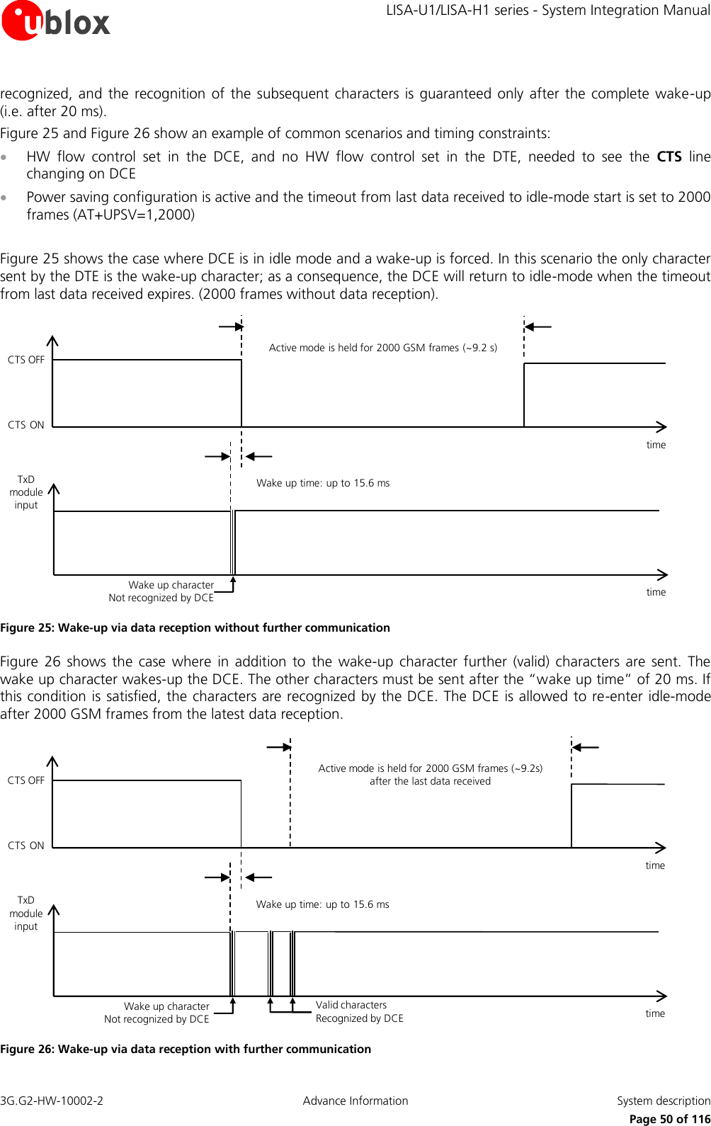
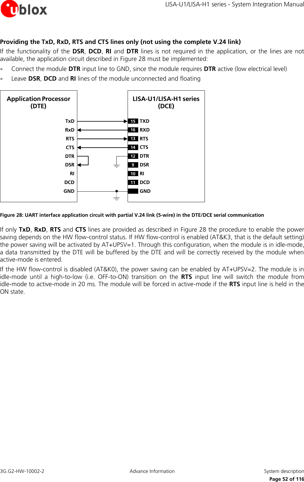
![LISA-U1/LISA-H1 series - System Integration Manual 3G.G2-HW-10002-2 Advance Information System description Page 51 of 116 The “wake-up via data reception” feature can’t be disabled. The “wake-up via data reception” feature can be used in both +UPSV=1 and +UPSV=2 case (when RTS line is set to OFF). In command mode, if HW flow control is not implemented by the DTE, the DTE must always send a dummy “AT” to the module before each command line: the first character will not be ignored if the module is in active-mode (i.e. the module will reply “OK”), or it will represent the wake up character if the module is in idle-mode (i.e. the module won’t reply). No dummy “AT” is required from the DTE during connected-mode since the module continues to be in active-mode and doesn’t need to be woken-up. Furthermore in data mode a dummy “AT” would affect the data communication. 1.9.2.4 UART application circuits Providing the full RS-232 functionality (using the complete V.24 link) For complete RS-232 functionality conforming to ITU Recommendation [3] in DTE/DCE serial communication, the complete UART interface of the module (DCE) must be connected to the DTE as described in Figure 27. LISA-U1/LISA-H1 series (DCE)TxDApplication Processor(DTE)RxDRTSCTSDTRDSRRIDCDGND15 TXD12 DTR16 RXD13 RTS14 CTS9DSR10 RI11 DCDGND Figure 27: Interface application circuit with complete V.24 link in DTE/DCE serial communication](https://usermanual.wiki/u-blox/LISAU120/User-Guide-1470694-Page-51.png)
![LISA-U1/LISA-H1 series - System Integration Manual 3G.G2-HW-10002-2 Advance Information System description Page 54 of 116 firmware upgrade over USB and for debug purpose. In both cases, provide as well access to RESET_N pin, or to the PWR_ON pin, or enable the DC supply connected to the VCC pin to start the module firmware upgrade (see Firmware Update Application Note [14]). If the UART interface is not used, all the UART interface pins can be left unconnected, but it is highly recommended to provide direct access to the RxD, TxD, CTS and RTS lines for execution of firmware upgrade and for debug purpose. 1.9.3 USB interface LISA-U1/LISA-H1 series modules provide a high-speed USB interface at 480 Mb/s compliant with the Universal Serial Bus Revision 2.0 specification [7]. It acts as a USB device and can be connected to any USB host such as a PC or other Application Processor. The USB-device shall look for all upper-SW-layers like any other serial device. This means that LISA-U1/LISA-H1 series modules emulate all serial control logical lines. If the logical DTR line isn't enabled by the USB host, the module doesn’t answer to AT commands by the USB interface. Name Description Remarks VUSB_DET USB detect input Apply 5 V typical to enable USB USB_D+ USB Data Line D+ 90 Ω nominal differential impedance. Pull-up or pull-down resistors and external series resistors as required by the USB 2.0 high-speed specification [7] are part of the USB pad driver and need not be provided externally. USB_D- USB Data Line D- 90 Ω nominal differential impedance. Pull-up or pull-down resistors and external series resistors as required by the USB 2.0 high-speed specification [7] are part of the USB pad driver and need not be provided externally. Table 20: USB pins The USB interface pins ESD rating is 1 kV (contact discharge). A higher protection level could be required if the lines are externally accessible on the application board. A higher protection level can be achieved mounting a very low capacitance ESD protection (e.g. Tyco Electronics PESD0402-140 ESD protection device) on the lines connected to these pins. 1.9.3.1 USB features LISA-U1/LISA-H1 series modules simultaneously support 6 USB CDC (Communications Device Class) that assure multiple functionalities to the USB physical interface. The 6 available CDCs are configured as described in the following list: USB1: AT commands / data connection USB2: AT commands / data connection USB3: AT commands / data connection USB4: GPS tunneling dedicated port USB5: 2G trace dedicated port USB6: 3G trace dedicated port LISA-U1/LISA-H1 series module identifies itself by its VID (Vendor ID) and PID (Product ID) combination, included in the USB device descriptor. VID and PID of LISA-U1/LISA-H1 series modules are the following: VID = 0x1546 PID = 0x1101](https://usermanual.wiki/u-blox/LISAU120/User-Guide-1470694-Page-54.png)
![LISA-U1/LISA-H1 series - System Integration Manual 3G.G2-HW-10002-2 Advance Information System description Page 55 of 116 If the USB interface of LISA-U1/LISA-H1 series modules is connected to the host before the module switch-on, or if the module is reset with the USB interface connected to the host, the VID and PID are automatically updated runtime, after the USB detection. First, VID and PID are the following: VID = 0x058B PID = 0x0041 Then, after a time period (~5 s), VID and PID are updated to the following: VID = 0x1546 PID = 0x1101 If power saving is enabled by AT command (AT+UPSV=1 or AT+UPSV=2), the LISA-U1/LISA-H1 series module automatically enters the USB suspended state when the device has observed no bus traffic for a specified period (refer to the Universal Serial Bus Revision 2.0 specification [7]). In suspended state, the module maintains any internal status as USB device, including its address and configuration. In addition, the module enters the suspended state when the hub port it is attached to is disabled: this is referred to as USB selective suspend. The module exits suspend mode when there is bus activity. LISA-U1/LISA-H1 series module is capable of USB remote wake-up signaling: may request the host to exit suspend mode or selective suspend by using electrical signaling to indicate remote wake-up. This notifies the host that it should resume from its suspended mode, if necessary, and service the external event that triggered the suspended USB device to signal the host. Remote wake-up is accomplished using electrical signaling described in the Universal Serial Bus Revision 2.0 specification [7]. 1.9.3.2 USB application circuit Since the module acts as a USB device, the USB supply (5.0 V typ.) must be provided to VUSB_DET by the connected USB host. The USB interface is enabled only when a valid voltage as USB supply is detected by the VUSB_DET input. Neither the USB interface, nor the whole module is supplied by the VUSB_DET input: the VUSB_DET senses the USB supply voltage and absorbs few microamperes. The USB_D+ and USB_D- lines carry the USB serial data and signaling. The lines are used in single ended mode for relatively low speed signaling handshake, as well as in differential mode for fast signaling and data transfer. USB pull-up or pull-down resistors on pins USB_D+ and USB_D- as required by the Universal Serial Bus Revision 2.0 specification [7] are part of the USB pad driver and do not need to be externally provided. External series resistors on pins USB_D+ and USB_D- as required by the Universal Serial Bus Revision 2.0 specification [7] are also integrated: characteristic impedance of USB_D+ and USB_D- lines is specified by the USB standard. The most important parameter is the differential characteristic impedance applicable for odd-mode electromagnetic field, which should be as close as possible to 90 differential: signal integrity may be degraded if the PCB layout is not optimal, especially when the USB signaling lines are very long. LISA-U1/LISA-H1 series VBUSD+D-GND18 VUSB_DET27 USB_D+26 USB_D-GNDC1USB DEVICE CONNECTORD1 D2 D3 Figure 30: USB Interface application circuit](https://usermanual.wiki/u-blox/LISAU120/User-Guide-1470694-Page-55.png)
![LISA-U1/LISA-H1 series - System Integration Manual 3G.G2-HW-10002-2 Advance Information System description Page 56 of 116 Reference Description Part Number - Manufacturer D1, D2, D3 Very Low Capacitance ESD Protection PESD0402-140 - Tyco Electronics C2 100 nF Capacitor Ceramic X7R 0402 10% 16 V GRM155R61A104KA01 - Murata Table 21: Component for USB application circuit If the USB interface is not connected to the application processor, it is highly recommended to provide direct access to the VUSB_DET, USB_D+, USB_D- lines for execution of firmware upgrade over USB and for debug purpose: testpoints can be added on the lines to accommodate the access. Otherwise, if the USB interface is connected to the application processor, it is highly recommended to provide direct access to the RxD, TxD, CTS and RTS lines for execution of firmware upgrade over UART and for debug purpose. In both cases, provide as well access to RESET_N pin, or to the PWR_ON pin, or enable the DC supply connected to the VCC pin to start the module firmware upgrade (see Firmware Update Application Note [14]). If the USB interface is not used, the USB_D+, USB_D- and VUSB_DET pins can be left unconnected, but it is highly recommended to provide direct access to the lines for execution of firmware upgrade and for debug purpose. 1.9.4 SPI interface SPI is a master-slave protocol: the module runs as an SPI slave, i.e. it accepts AT commands on its SPI interface without specific configuration. The SPI-compatible synchronous serial interface cannot be used for FW upgrade. The standard 3-wire SPI interface includes two signals to transmit and receive data (SPI_MOSI and SPI_MISO) and a clock signal (SPI_SCLK). LISA-U1/LISA-H1 series modules provide two handshake signals (SPI_MRDY and SPI_SRDY), added to the standard 3-wire SPI interface, implementing the 5-wire Inter Processor Communication (IPC) interface. The purpose of the IPC interface is to achieve high speed communication (up to 20 Mb/s) between two processors following the same IPC specifications: the module baseband processor and an external processor. The high speed communication is possible only if both sides follow the same Inter Processor Communication (IPC) specifications. This interface is designated for high speed HSPA communications and could be necessary to communicate with an Application Processor which is not equipped with a USB interface.](https://usermanual.wiki/u-blox/LISAU120/User-Guide-1470694-Page-56.png)
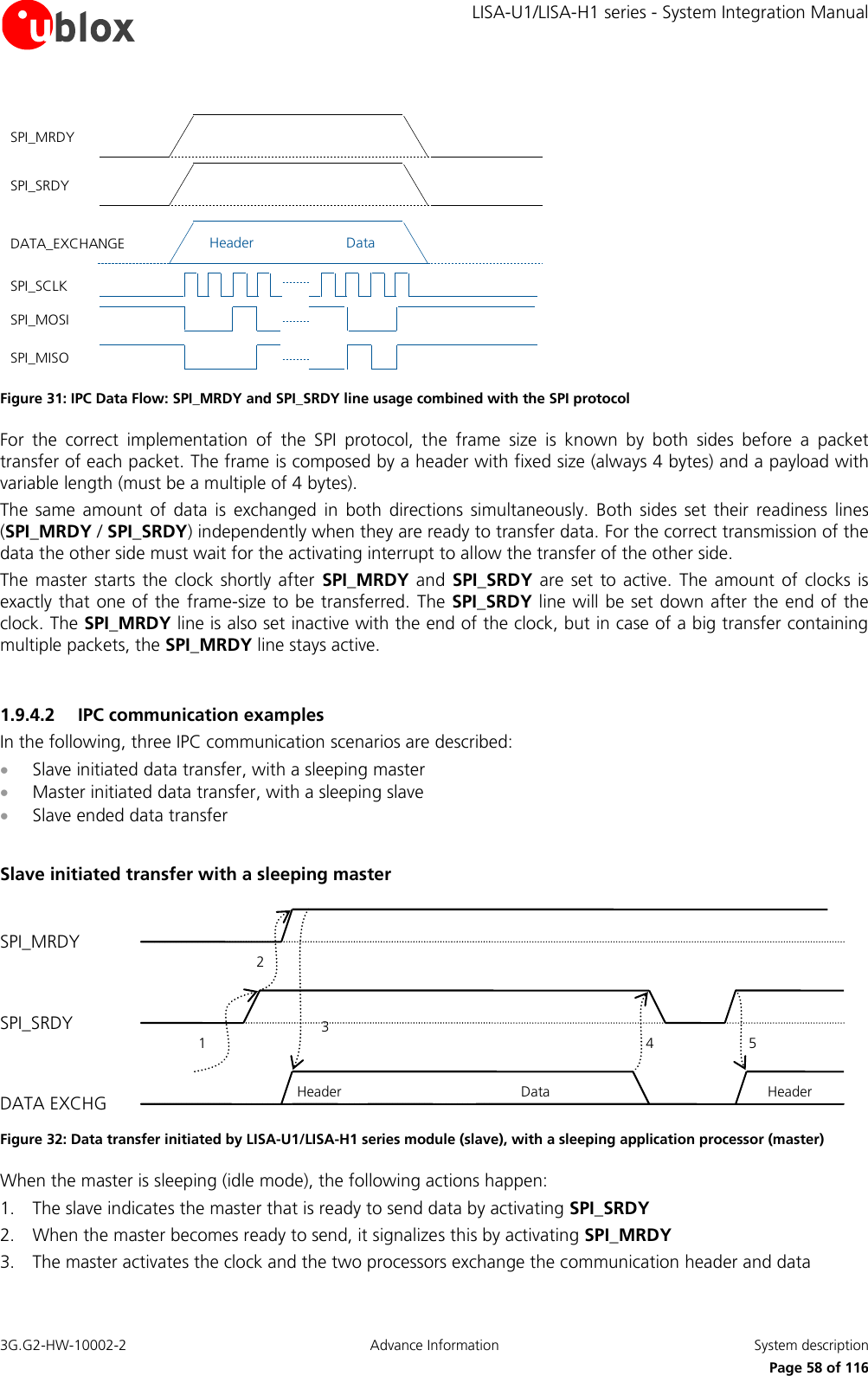
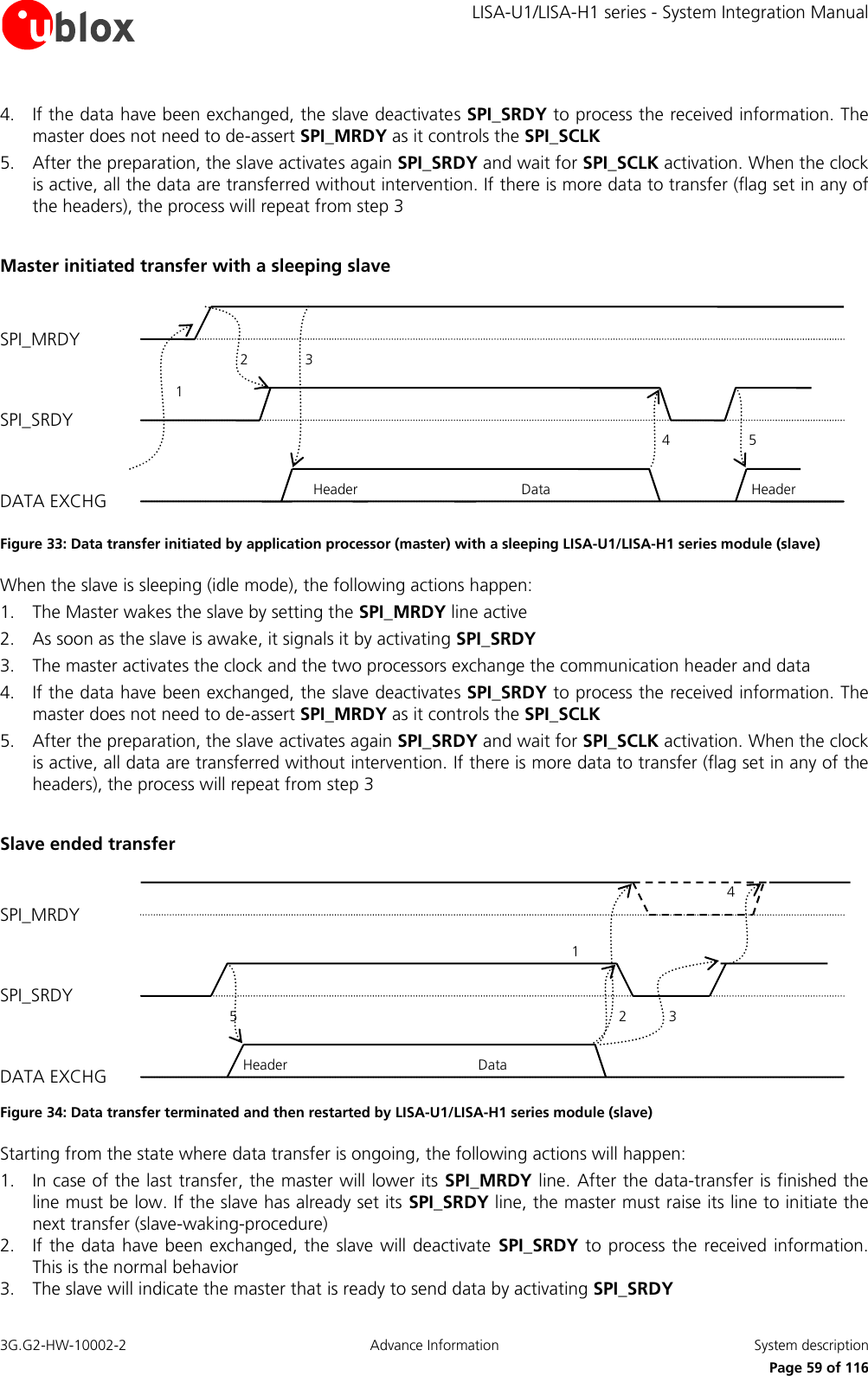
![LISA-U1/LISA-H1 series - System Integration Manual 3G.G2-HW-10002-2 Advance Information System description Page 60 of 116 4. When the master is ready to send, it will signalize this by activating SPI_MRDY. This is optional, when SPI_MRDY is low before 5. The slave indicates immediately after a transfer termination that it wants to start transmission again. In this case the slave will raise SPI_SRDY again. The SPI_MRDY line can be either high or low: the master has only to ensure that the SPI_SRDY change will be detected correctly via interrupt For more details regarding IPC communication protocol please refer to SPI Application Note [18]. 1.9.4.3 IPC application circuit SPI_MOSI is the data line input for the module since it runs as SPI slave: it must be connected to the data line output (MOSI) of the application processor that runs as an SPI master. SPI_MISO is the data line output for the module since it runs as SPI slave: it must be connected to the data line input (MISO) of the application processor that runs as an SPI master. SPI_SCLK is the clock input for the module since it runs as SPI slave: it must be connected to the clock line output (SCLK) of the application processor that runs as an SPI master. SPI_MRDY is an input for the module able to detect an external interrupt which comes from the application processor. SPI_SRDY is an output for the module, and the application processor should be able to detect an external interrupt which comes from the module on its connected pin. Signal integrity of the high speed data lines may be degraded if the PCB layout is not optimal, especially when the SPI lines are very long: keep routing short and minimize parasitic capacitance to preserve signal integrity. LISA-U1/LISA-H1 series (SPI slave)MOSIApplication Processor(SPI master)MISOSCLKInterruptGPIOGND56 SPI_MOSI59 SPI_MRDY57 SPI_MISO55 SPI_SCLK58 SPI_SRDYGND Figure 35: IPC Interface application circuit If direct access to the USB or the UART interfaces of the module is not provided, it is recommended to provide direct access to the SPI_MOSI, SPI_MISO, SPI_SCLK, SPI_MRDY, SPI_SRDY lines of the module for debug purpose: testpoints can be added on the lines to accommodate the access and a 0 Ω series resistor must be mounted on each line to detach the module pin from any other connected device. If the SPI/IPC interface is not used, the SPI_MOSI, SPI_MISO, SPI_SCLK, SPI_MRDY, SPI_SRDY pins can be left unconnected. 1.9.5 MUX Protocol (3GPP 27.010) The LISA-U1/LISA-H1 series module has a software layer with MUX functionality, 3GPP TS 27.010 Multiplexer Protocol [6], available on the UART and on the SPI physical link. This is a data link protocol (layer 2 of OSI model) which uses HDLC-like framing and operates between the module (DCE) and the application processor (DTE) and allows a number of simultaneous sessions over the used](https://usermanual.wiki/u-blox/LISAU120/User-Guide-1470694-Page-60.png)
![LISA-U1/LISA-H1 series - System Integration Manual 3G.G2-HW-10002-2 Advance Information System description Page 61 of 116 physical link (UART or SPI). Each session consists of a stream of bytes transferring various kinds of data such as SMS, CBS, GPRS, GPS, AT commands in general. This permits, for example, SMS to be transferred to the DTE when a data connection is in progress. The following virtual channels are defined: Channel 0: control channel Channel 1 – 5: AT commands /data connection Channel 6: GPS tunneling For more details please refer to GSM Mux implementation Application Note [15]. 1.10 DDC (I2C) interface 1.10.1 Overview An I2C compatible Display Data Channel (DDC) interface for serial communication is implemented. This interface is dedicated exclusively to access u-blox GPS receivers. Name Description Remarks SCL I2C bus clock line Open drain. External pull-up required. SDA I2C bus data line Open drain. External pull-up required. Table 23: DDC pins The DDC (I2C) interface pins ESD rating is 1 kV (contact discharge). A higher protection level could be required if the lines are externally accessible on the application board. A higher protection level can be achieved mounting an ESD protection (e.g. EPCOS CA05P4S14THSG varistor array) on the lines connected to these pins. To be compliant to the I2C bus specifications, the module bus interface pads are open drain output and pull up resistors must be used. Since the pull-up resistors are not mounted on the module, they must be mounted externally. Resistor values must conform to the I2C bus specifications [8]. If a LISA-U1/LISA-H1 series module is connected through the DDC bus to a single u-blox GPS receiver only (only one device is connected on the DDC bus), use a pull-up resistor of 4.7 k. Pull-ups must be connected to a supply voltage of 1.8 V (typical), since this is the voltage domain of the DDC pins. V_INT digital interfaces supply output can be used to provide 1.8 V for the pull-ups (for detailed electrical characteristics see the LISA-U1/LISA-H1 series Data Sheet [1]). DDC Slave-mode operation is not supported, the module can act as master only. Two lines, serial data (SDA) and serial clock (SCL), carry information on the bus. SCL is used to synchronize data transfers, and SDA is the data line. Since both lines are open drain outputs, the DDC devices can only drive them low or leave them open. The pull-up resistor pulls the line up to the supply rail if no DDC device is pulling it down to GND. If the pull-ups are missing, SCL and SDA lines are undefined and the DDC bus will not work. The signal shape is defined by the values of the pull-up resistors and the bus capacitance. Long wires on the bus will increase the capacitance. If the bus capacitance is increased, use pull-up resistors with nominal resistance value lower than 4.7 k, to match the I2C bus specifications [8].regarding rise and fall times of the signals. Capacitance and series resistance must be limited on the bus to match the I2C specifications (1.0 µs is the maximum allowed rise time on the SCL and SDA lines): route connections as short as possible.. If the pins are not used as DDC bus interface, they can be left unconnected.](https://usermanual.wiki/u-blox/LISAU120/User-Guide-1470694-Page-61.png)
![LISA-U1/LISA-H1 series - System Integration Manual 3G.G2-HW-10002-2 Advance Information System description Page 62 of 116 1.10.2 DDC application circuit The SDA and SCL lines can be used only to connect the LISA module to a u-blox GPS module: LISA DDC (I2C) interface is enabled by the +UGPS AT command (for more details refer to u-blox AT Commands Manual [2]). GPIO2 is automatically driven as an output by the +UGPS AT command to switch-on or to switch-off the u-blox GPS module, connecting GPIO2 to the active-high enable pin (or the active-low shutdown pin) of the voltage regulator that supplies the u-blox GPS module on the application board. GPIO3 is automatically driven as an input by the +UGPS AT command to sense when the u-blox GPS module is ready to send data. GPIO4 is automatically driven as an output by the +UGPS AT command to provide a synchronization timing signal to the u-blox GPS module. The application circuit for the connection of a LISA-U1/LISA-H1 series wireless module to a u-blox 1.8 V GPS receiver is illustrated in Figure 36. A pull-down resistor is mounted on the GPIO2 line to avoid a switch on of the GPS module when the LISA-U1/LISA-H1 series module is in the internal reset state. LISA-U1/LISA-H1 seriesR1INOUTGNDGPS LDORegulatorSHDNu-blox1.8 V GPS receiverSDA2SCL2R21V8 1V8VMAIN1V8U121 GPIO2SDASCLC1TxD1EXTINT0GPIO3GPIO446452324VCCR3 Figure 36: DDC Application circuit for u-blox 1.8 V GPS receiver Reference Description Part Number - Manufacturer R1, R2, R3 4.7 kΩ Resistor 0402 5% 0.1 W RC0402JR-074K7L - Yageo Phycomp U1 Voltage Regulator for GPS Receiver See GPS Receiver Hardware Integration Manual Table 24: Components for DDC application circuit for u-blox 1.8 V GPS receiver If a 3 V u-blox GPS receiver is used, the SDA, SCL pins and the GPIO2, GPIO3, GPIO4 pins of the LISA-U1/LISA-H1 series wireless module cannot be directly connected to the 3 V u-blox GPS receiver, since the pins of the LISA-U1/LISA-H1 series modules aren’t tolerant up to 3 V. An application circuit for the connection of a LISA-U1/LISA-H1 series wireless module to a u-blox 3.0 V GPS receiver is illustrated in Figure 37. A pull-down resistor is mounted on the GPIO2 line to avoid a switch on of the GPS module when the LISA-U1/LISA-H1 series module is in the internal reset state.](https://usermanual.wiki/u-blox/LISAU120/User-Guide-1470694-Page-62.png)
![LISA-U1/LISA-H1 series - System Integration Manual 3G.G2-HW-10002-2 Advance Information System description Page 63 of 116 LISA-U1/LISA-H1 seriesR1INOUTGNDGPS LDORegulatorSHDNu-blox3.0 V GPS receiverR2VMAIN3V0U121 GPIO246 SDA45 SCLR4 R51V8SDA1 SDA2GNDU2SCL1SCL2VREF1VREF2I2C-busBidirectional Voltage Translator21 V_INTC1C2 C3R323 GPIO324 GPIO41V8A1 B1GNDU3A2B2VCCAVCCBGenericBidirectional Voltage TranslatorC4 C53V0SDA2SCL2TxD1EXTINT0VCC Figure 37: DDC Application circuit for u-blox 3.0 V GPS receiver Reference Description Part Number - Manufacturer R1, R2, R3, R4, R5 4.7 kΩ Resistor 0402 5% 0.1 W RC0402JR-074K7L - Yageo Phycomp C2, C3, C4, C5 100 nF Capacitor Ceramic X5R 0402 10% 10V GRM155R71C104KA01 - Murata U1 Voltage Regulator for GPS Receiver See GPS Receiver Hardware Integration Manual U2 I2C-bus Bidirectional Voltage Translator PCA9306DCURG4 - Texas Instruments U3 Generic Bidirectional Voltage Translator TXB0104PWR - Texas Instruments Table 25: Components for DDC application circuit for u-blox 3.0 V GPS receiver 1.11 Audio Interface (LISA-U120 and LISA-U130 only) LISA-U120 and LISA-U130 modules provide analog and digital audio interfaces: One differential analog audio input (microphone input) One differential analog audio output (speaker output) One 4-wire I2S digital audio interface: input and output Audio signal routing can be controlled by the dedicated AT command +USPM (refer to u-blox AT Commands Manual [2]). This command allows setting the audio path mode, composed by the uplink audio path and the downlink audio path.](https://usermanual.wiki/u-blox/LISAU120/User-Guide-1470694-Page-63.png)
![LISA-U1/LISA-H1 series - System Integration Manual 3G.G2-HW-10002-2 Advance Information System description Page 64 of 116 Each uplink path mode defines the physical input (i.e. the analog or the digital audio input) and the set of parameters to process the uplink audio signal (uplink gains, uplink digital filters, echo canceller parameters). For example the “Headset microphone” uplink path uses the differential analog audio input with the default parameters for the headset profile. Each downlink path mode defines the physical output (i.e. the analog or the digital audio output) and the set of parameters to process the downlink audio signal (downlink gains, downlink digital filters and sidetone). For example the “Mono headset” downlink path uses the differential analog audio output with the default parameters for the headset profile. The set of parameters to process the uplink or the downlink audio signal can be changed with dedicated AT commands for each uplink or downlink path and then stored in two profiles in the non volatile memory (refer to u-blox AT Commands Manual [2] for Audio parameters tuning commands). 1.11.1 Analog Audio interface 1.11.1.1 Uplink path (differential analog audio input) The pins related to the differential analog audio input are: MIC_P / MIC_N: Differential analog audio signal inputs (positive/negative). These two pins are provided with internal series 100 nF capacitors for DC blocking that connect the module pads to the differential input of a Low Noise Amplifier. The LNA output is internally connected to the digital processing system by an integrated sigma-delta analog-to-digital converter The analog audio input is selected when the parameter <main_uplink> in AT+USPM command is set to “Headset microphone”, “Handset microphone” or “Hands-free microphone”: the uplink analog path profiles use the same physical input but have different sets of audio parameters (for more details please refer to u-blox AT Commands Manual [2], AT+USPM, AT+UMGC, AT+UUBF, AT+UHFP commands). There is no microphone supply pin available on the module: an external low noise LDO voltage regulator should be added to provide a proper supply for a microphone. Detailed electrical characteristics of the differential analog audio input can be found in the LISA-U1/LISA-H1 series Data Sheet [1]. 1.11.1.2 Downlink path (differential analog audio output) The pins related to the differential analog audio output are: SPK_N / SPK_P: Differential analog audio signal output (positive/negative). These two pins are internally directly connected to the differential output of a low power audio amplifier, for which the input is internally connected to the digital processing system by to an integrated digital-to-analog converter. The analog audio output is selected when the parameter <main_downlink> in AT+USPM command is set to “Normal earpiece”, “Mono headset” or “Loudspeaker”: the downlink analog path profiles use the same physical output but have different sets of audio parameters (for more details please refer to u-blox AT Commands Manual [2], AT+USPM, AT+USGC, AT+UDBF, AT+USTN commands). The differential analog audio output can be directly connected to a headset earpiece or handset earpiece but is not able to drive an 8 speaker. Detailed electrical characteristics of the high power differential audio output can be found in the LISA-U1/LISA-H1 series Data Sheet [1]. Warning: excessive sound pressure from headphones can cause hearing loss.](https://usermanual.wiki/u-blox/LISAU120/User-Guide-1470694-Page-64.png)
![LISA-U1/LISA-H1 series - System Integration Manual 3G.G2-HW-10002-2 Advance Information System description Page 65 of 116 Table 26 lists the signals related to analog audio functions. Name Description Remarks MIC_P Differential analog audio input (Positive) Shared for all uplink analog path modes: handset, headset, hands-free mode. Internal DC blocking capacitor. MIC_N Differential analog audio input (Negative) Shared for all uplink analog path modes: handset, headset, hands-free mode. Internal DC blocking capacitor. SPK_P Differential analog audio output (Positive) Shared for all uplink analog path modes: earpiece, headset, loudspeaker mode. SPK_N Differential analog audio output (Negative) Shared for all uplink analog path modes: earpiece, headset, loudspeaker mode. Table 26: Analog Audio Signal Pins The audio pins ESD rating is 1 kV (contact discharge). A higher protection level could be required if the lines are externally accessible on the application board. A higher protection level can be achieved mounting an ESD protection (e.g. EPCOS CA05P4S14THSG varistor array) on the lines connected to these pins. All corresponding differential audio lines must be routed in pairs, be embedded in GND (have the ground lines as close as possible to the audio lines), and maintain distance from noisy lines such as VCC and from components such as switching regulators. If the audio pins are not used, they can be left unconnected on the application board. 1.11.1.3 Headset mode Headset mode is the default audio operating mode of the LISA-U120 and LISA-U130 modules. The headset profile is configured when the uplink audio path is set to “Headset microphone” and the downlink audio path is set to “Mono headset” (refer to u-blox AT Commands Manual [2]: AT+USPM command: <main_uplink>, <main_downlink> parameters): Headset microphone must be connected to the module differential input MIC_P / MIC_N Headset receiver must be connected to the module differential output SPK_P / SPK_N Figure 38 shows an example of an application circuit connecting a headset (with a 2.2 k electret microphone and a 32 receiver) to the LISA-U120 and LISA-U130 modules, with an external low noise LDO voltage regulator to provide a proper supply for the microphone. Mount an 82 nH series inductor (e.g. Murata LQG15HS82NJ02) on each microphone line, and a 27 pF bypass capacitor (e.g. Murata GRM1555C1H270J) on all audio lines to minimize RF coupling and TDMA noise. The physical width of the audio outputs lines on the application board must be wide enough to minimize series resistance.](https://usermanual.wiki/u-blox/LISAU120/User-Guide-1470694-Page-65.png)
![LISA-U1/LISA-H1 series - System Integration Manual 3G.G2-HW-10002-2 Advance Information System description Page 66 of 116 LISA-U120/U130C2 C3 C4J1253461L254SPK_N53SPK_P39MIC_N40MIC_PD1AUDIO HEADSET CONNECTORD2INOUTGNDLow Noise LDO Regulator VMAINU1R4R1C6R3R2 C52V5Sense lines connected to GND in one star pointL1C1C7 Figure 38: Headset mode application circuit Reference Description Part Number - Manufacturer C1, C2, C3, C4 27 pF Capacitor Ceramic COG 0402 5% 25 V GRM1555C1H270JA01 - Murata C5, C6, C7 10 µF Capacitor Ceramic X5R 0603 20% 6.3 V GRM188R60J106ME47 - Murata D1, D2 Low Capacitance ESD Protection USB0002RP or USB0002DP - AVX L1, L2 82 nH Multilayer inductor 0402 (self resonance frequency ~1 GHz) LQG15HS82NJ02 - Murata J1 Audio Headset 2.5 mm Jack Connector SJ1-42535TS-SMT – CUI, Inc. R1, R2, R3, R4 2.2 kΩ Resistor 0402 5% 0.1 W RC0402JR-072K2L - Yageo Phycomp U1 Low Noise LDO Linear Regulator 2.5 V 300 mA LT1962EMS8-2.5#PBF- Linear Technology Table 27: Example of components for headset jack connection 1.11.1.4 Handset mode The handset profile is configured when the uplink audio path is set to “Handset microphone” and the downlink audio path is set to “Normal earpiece” (refer to u-blox AT commands manual [2]: AT+USPM command: <main_uplink>, <main_downlink> parameters): Handset microphone must be connected to the module differential input MIC_P / MIC_N Handset receiver must be connected to the module differential output SPK_P / SPK_N Figure 39 shows an example of an application circuit connecting a handset (with a 2.2 k electret microphone and a 32 receiver) to the LISA-U120 and LISA-U130 modules, with an external low noise LDO voltage regulator to provide a proper supply for the microphone. Mount an 82 nH series inductor (e.g. Murata LQG15HS82NJ02) on each microphone line and a 27 pF bypass capacitor (e.g. Murata GRM1555C1H270J) on all audio lines to minimize RF coupling and TDMA noise. The physical width of the audio outputs lines on the application board must be wide enough to minimize series resistance.](https://usermanual.wiki/u-blox/LISAU120/User-Guide-1470694-Page-66.png)
![LISA-U1/LISA-H1 series - System Integration Manual 3G.G2-HW-10002-2 Advance Information System description Page 67 of 116 LISA-U120/U130C1 C2 C3 J14321L153SPK_P54SPK_N40MIC_P39MIC_ND1AUDIO HANDSET CONNECTORD2INOUTGNDLow Noise LDO RegulatorU1R4R1C6R3R2 C52V5Sense lines connected to GND in one star pointC4L2VMAINC7 Figure 39: Handset mode application circuit Reference Description Part Number - Manufacturer C1, C2, C3, C4 27 pF Capacitor Ceramic COG 0402 5% 25 V GRM1555C1H270JA01 - Murata C5, C6, C7 10 µF Capacitor Ceramic X5R 0603 20% 6.3 V GRM188R60J106ME47 - Murata D1, D2 Low Capacitance ESD Protection USB0002RP or USB0002DP - AVX L1, L2 82nH Multilayer inductor 0402 (self resonance frequency ~1 GHz) LQG15HS82NJ02 - Murata J1 Audio Handset Jack Connector, 4Ckt (4P4C) 52018-4416 - Molex R1, R2, R3, R4 2.2 kΩ Resistor 0402 5% 0.1 W RC0402JR-072K2L - Yageo Phycomp U1 Low Noise LDO Linear Regulator 2.5 V 300 mA LT1962EMS8-2.5#PBF- Linear Technology Table 28: Example of components for handset connection 1.11.1.5 Hands-free mode The hands-free profile is configured when the uplink audio path is set to “Hands-free microphone” and the downlink audio path is set to “Loudspeaker” (refer to u-blox AT commands manual [2]: AT+USPM command: <main_uplink>, <main_downlink> parameters): Hands-free microphone signal must be connected to the module differential input MIC_P / MIC_N High power loudspeaker must be connected to the output of an external audio amplifier, for which the input must be connected to the module differential output SPK_P / SPK_N The module differential analog audio output is not able to drive an 8 speaker: an external audio amplifier must be provided on the application board to amplify the low power audio signal provided by the module differential output SPK_P / SPK_N. Hands-free functionality is implemented using appropriate digital signal processing algorithms for voice-band handling (echo canceller and automatic gain control), managed via software (refer to u-blox AT commands manual [2], AT+UHFP command). Figure 39 shows an example of an application circuit connecting a 2.2 k electret microphone and an 8 speaker to the LISA-U120 and LISA-U130 modules, with an external low noise LDO voltage regulator to provide a proper supply for the microphone and with an external audio amplifier to amplify the low power audio signal provided by the module differential output.](https://usermanual.wiki/u-blox/LISAU120/User-Guide-1470694-Page-67.png)
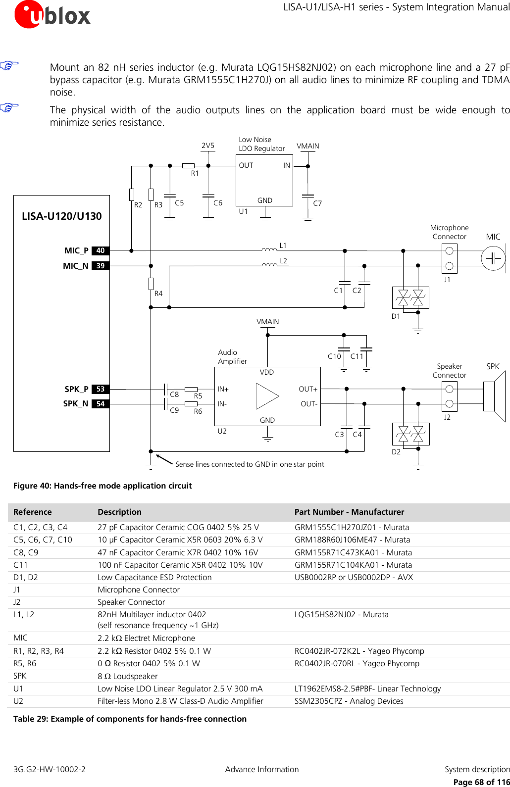
![LISA-U1/LISA-H1 series - System Integration Manual 3G.G2-HW-10002-2 Advance Information System description Page 69 of 116 1.11.1.6 Connection to an external analog audio device The differential analog audio input / output can be used to connect the module to an external analog audio device. Audio devices with a differential analog input / output are preferable, as they are more immune to external disturbances. If the external analog audio device is provided with a differential analog audio input, the SPK_P / SPK_N balanced output of the module must be connected to the differential input of the external audio device through a DC-block 10 µF series capacitor (e.g. Murata GRM188R60J106M) to decouple the bias present at the module output (see SPK_P / SPK_N common mode output voltage in the LISA-U1/LISA-H1 series Data Sheet [1]). Use a suitable power-on sequence to avoid audio bump due to charging of the capacitor: the final audio stage should be always enabled as last one. If the external analog audio device is provided with a single ended analog audio input, a proper differential to single ended circuit must be inserted from the SPK_P / SPK_N balanced output of the module to the single ended input of the external audio device. A simple application circuit is described in Figure 41: 10 µF series capacitors (e.g. Murata GRM188R60J106M) are provided to decouple the bias present at the module output, and a voltage divider is provided to properly adapt the signal level from the module output to the external audio device input. The DC-block series capacitor acts as high-pass filter for audio signals, with cut-off frequency depending on both the values of capacitor and on the input impedance of the external audio device. For example: in case of differential input impedance of 600 , the two 10 µF capacitors will set the -3 dB cut-off frequency to 53 Hz, while for single ended connection to 600 external device, the cut-off frequency with just the single 10 µF capacitor will be 103 Hz. In both cases the high-pass filter has a low enough cut-off to not impact the audio signal frequency response. The signal levels can be adapted by setting gain using AT commands, but additional circuitry must be inserted if the SPK_P / SPK_N output level of the module is too high for the input of the audio device. If the external analog audio device is provided with a differential analog audio output, the MIC_P / MIC_N balanced input of the module must be connected directly to the differential output of the external audio device. Series capacitors are not needed since MIC_P / MIC_N pins are provided with internal 100 nF capacitors for DC blocking (see LISA-U1 series Data Sheet [1]). If the external analog audio device is provided with a single ended analog audio output, a proper single ended to differential circuit has to be inserted from the single ended output of the external audio device to the MIC_P / MIC_N balanced input of the module. A simple application circuit is described in Figure 41: a voltage divider is provided to properly adapt the signal level from the external audio device output to the module input. The signal levels can be adapted by setting gain using AT commands, but additional circuitry must be inserted if the output level of the audio device is too high for MIC_P / MIC_N. Please refer to Figure 41 for the application circuits. To enable the audio path corresponding to the differential analog audio input / output, please refer to u-blox AT Commands Manual [2]: AT+USPM command. To tune audio levels for the external device please refer to u-blox AT Commands Manual [2] (AT+USGC, AT+UMGC commands).](https://usermanual.wiki/u-blox/LISAU120/User-Guide-1470694-Page-69.png)
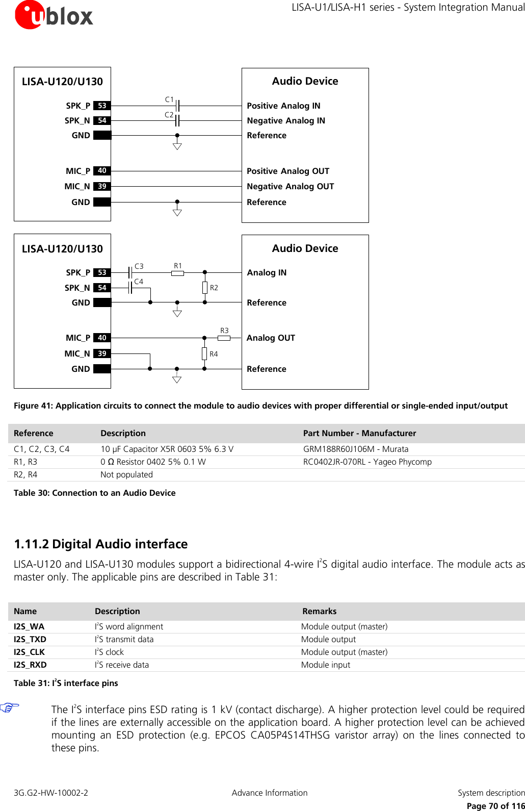
![LISA-U1/LISA-H1 series - System Integration Manual 3G.G2-HW-10002-2 Advance Information System description Page 71 of 116 If the I2S digital audio pins are not used, they can be left unconnected on the application board. The I2S interface can be can be used in two modes: PCM mode Normal I2S mode To select the I2S digital audio interface the AT+USPM command parameters must assume these values (for more details please refer to u-blox AT Commands Manual [2]): <main_uplink>: “I2S input line” <main_downlink>: “I2S output line” Parameters of digital path can be configured and saved as the normal analog paths, using appropriate path parameter as described in the u-blox AT Commands Manual [2], +USGC, +UMGC, +USTN AT command. Analog gain parameters of microphone and speakers are unused when digital path is selected. I2S_TX and I2S_RX are respectively parallel to the analog front end, so resources available for analog path can be shared: Digital filters and digital gains are available in both uplink and downlink direction. Configure using AT commands Ringer tone and service tone are mixed on the TX path when active (downlink) The HF algorithm acts on I2S path Refer to the u-blox AT Commands Manual [2]: AT+UI2S command for possible combinations of connection and settings. 1.11.2.1 I2S interface - PCM mode Main features of the I2S interface in PCM mode: I2S runs in PCM - short alignment mode (configurable by AT commands) Module functions as I2S master (I2S_CLK and I2S_WA signals generated by the module) I2S_WA signal always runs at 8 kHz I2S_WA toggles high for 1 or 2 CLK cycles of synchronization (configurable), then toggles low for 16 CLK cycles of sample width. Frame length can be 1 + 16 = 17 bits or 2 + 16 = 18 bits I2S_CLK frequency depends on frame length. Can be 17 x 8 kHz = 136 kHz or 18 x 8 kHz = 144 kHz I2S_TX, I2S_RX data are 16 bit words with 8 kHz sampling rate, mono. Data is in 2’s complement notation. MSB is transmitted first When I2S_WA toggles high, the first synchronization bit is always low. Second synchronization bit (present only in case of 2 bit long I2S_WA configuration) is MSB of the transmitted word (MSB is transmitted twice in this case) I2S_TX changes on I2S_CLK rising edge, I2S_RX changes on I2S_CLK falling edge 1.11.2.2 I2S interface - Normal I2S mode Normal I2S supports: 16 bits word Mono interface 8 kHz frequency Main features of I2S interface in normal I2S mode:](https://usermanual.wiki/u-blox/LISAU120/User-Guide-1470694-Page-71.png)
![LISA-U1/LISA-H1 series - System Integration Manual 3G.G2-HW-10002-2 Advance Information System description Page 72 of 116 I2S_WA signal always runs at 8 kHz and synchronizes 2 channels (timeslots on WA high, WA low) I2S_TX data are composed of 16 bit words, dual mono (the words are written on both channels). Data are in 2’s complement notation. MSB is transmitted first. The bits are written on I2S_CLK rising or falling edge (configurable) I2S_RX data are read as 16 bit words, mono (words are read only on the timeslot with WA high). Data is read in 2’s complement notation. MSB is read first. The bits are read on the I2S_CLK edge opposite to I2S_TX writing edge (configurable) I2S_CLK frequency is 16 bits x 2 channels x 8 kHz = 256 kHz The modes are configurable through a specific AT command (refer to the related chapter in u-blox AT Commands Manual [2], +UI2S AT command) and the following parameters can be set: MSB can be 1 bit delayed or non-delayed on I2S_WA edge I2S_TX data can change on rising or falling edge of I2S_CLK signal (rising edge in this example) I2S_RX data are read on the opposite front of I2S_CLK signal 1.11.3 Voiceband processing system The voiceband processing on the LISA-U120 and LISA-U130 modules is implemented in the DSP core inside the baseband chipset. The analog audio front-end of the chipset is connected to the digital system through 16 bit ADC converters in the uplink path, and through 16 bit DAC converters in the downlink path. External digital audio devices can be interfaced directly to the DSP digital processing part via the I2S digital interface. The analog amplifiers are skipped in this case. Possible processing of audio signal are: Speech encoding (uplink) and decoding (downlink).The following speech codecs are supported in firmware on the DSP: Fullrate, enhanced full rate, and half rate speech encoding and decoding Adaptive multi rate (full rate and half rate) speech encoding and decoding Mandatory sub-functions: Discontinuous transmission, DTX (GSM 46.031, 46.041, 46.081 and 46.093 standards) Voice activity detection, VAD (GSM 46.032, 46.042, 46.082 and 46.094 standards) Background noise calculation (GSM 46.012, 46.022, 46.062 and 46.092 standards) Function configurable via specific AT commands (refer to the u-blox AT Commands Manual [2]) Signal routing: +USPM command Analog amplification, Digital amplification: +USGC,+CLVL, +CRSL, +CMUT command Digital filtering: +UUBF, +UDBF commands Hands-free algorithms (echo cancellation, Noise suppression, Automatic Gain control) +UHFP command Sidetone generation (feedback of uplink speech signal to downlink path): +USTN command Playing/mixing of alert tones: Service tones: Tone generator with 3 sinus tones +UPAR command User generated tones: Tone generator with 3 sinus tones +UTGN command Midi melodies (for ringer): Synthesizer with up to 64 voices and a 48 kHz sampling rate, +UPAR command AMR files (for prompting): The storage format of AMR encoded audio content is defined in RFC3267 chapter 5 [9], +UPLAYFILE command With exception of the speech encoder/decoder, this audio processing can be controlled by AT commands. This processing is implemented within three different blocks of the voiceband processing system:](https://usermanual.wiki/u-blox/LISAU120/User-Guide-1470694-Page-72.png)
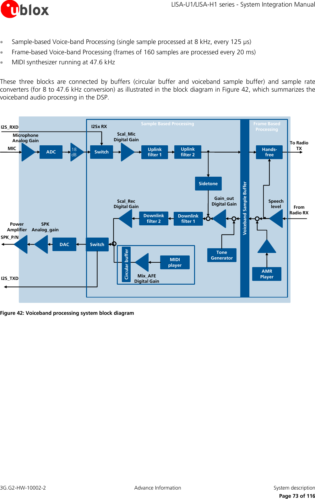
![LISA-U1/LISA-H1 series - System Integration Manual 3G.G2-HW-10002-2 Advance Information System description Page 74 of 116 1.12 General Purpose Input/Output (GPIO) The LISA-U1/LISA-H1 series modules provide 5 pins (GPIO1, GPIO2, GPIO3, GPIO4 and GPIO5) which can be configured as general purpose input or output, or can be configured to provide special functions via u-blox AT commands (for further details refer to u-blox AT Commands Manual [2], +UGPIOC, +UGPIOR, +UGPIOW, +UGPS, +UGPRF). The available functions are described below: GSM Tx burst indication: the GPIO1 can be configured by AT+UGPIOC to indicate when a GSM Tx burst/slot occurs. The pin can be connected on the application board to an input pin of an application processor to indicate when a GSM Tx burst/slot occurs GPS supply enable: the GPIO2 is by default configured to enable or disable the supply of the u-blox GPS receiver connected to the LISA-U1/LISA-H1 series module. The pin must be connected to the active-high enable pin (or the active-low shutdown pin) of the voltage regulator that supplies the u-blox GPS receiver on the application board. The pin is automatically set output high to switch on the u-blox GPS receiver when the parameter <mode> of +UGPS AT command is set to 1, and otherwise it is set in tri-state with an internal active pull-down enabled. The GPIO1, GPIO3, GPIO4 or GPIO5 can be configured by AT+UGPIOC to provide this feature, alternatively to the default GPIO2 GPS data ready: the GPIO3 is by default configured to sense when the u-blox GPS receiver connected to the LISA-U1/LISA-H1 series module is ready to send data by the DDC (I2C) interface. The pin must be connected to the data ready output of the u-blox GPS receiver (i.e. the pin TxD1 of the u-blox GPS module) on the application board. The pin automatically senses the line status to wake up the LISA-U1/LISA-H1 series module from idle mode if the u-blox GPS receiver is ready to send data by the DDC (I2C) interface, when the parameter <mode> of +UGPS AT command is set to 1, and otherwise it is set in tri-state with an internal active pull-down enabled GPS aiding synch: the GPIO4 is by default configured to provide a synchronization timing signal to the u-blox GPS receiver connected to the LISA-U1/LISA-H1 series module. The pin must be connected to the synchronization timing input of the u-blox GPS receiver (i.e. the pin EXTINT0 of the u-blox GPS module) on the application board. The pin automatically provides a synchronization timing signal to the u-blox GPS receiver when the parameter <mode> of +UGPS AT command is set to 1, and otherwise it is set in tri-state with an internal active pull-down enabled SIM card detection: the GPIO5 is by default configured to detect SIM card presence. The pin must be connected on the application board to the SW2 pin of the SIM card connector with a 470 kΩ pull-down resistor and SW1 pin of the SIM card connector must be pulled up to the module V_INT by a 1 kΩ pull-up resistor Network status indication: each GPIO (GPIO1, GPIO2, GPIO3, GPIO4 or GPIO5) can be configured by AT+UGPIOC to indicate network status (registered home network, registered roaming, data transmission, no service). The pin configured to provide this feature can be connected on the application board to an input pin of an application processor or can drive a LED by a transistor with integrated resistors to indicate network status General purpose input: all the GPIOs (GPIO1, GPIO2, GPIO3, GPIO4 and GPIO5) can be configured by AT+UGPIOC as input, sensing high or low digital level by AT+UGPIOR General purpose output: all the GPIOs (GPIO1, GPIO2, GPIO3, GPIO4 and GPIO5) can be configured by AT+UGPIOC as output, set in the high or low digital level by AT+UGPIOW, sensing high or low digital level by AT+UGPIOR Pad disabled: all the GPIOs (GPIO1, GPIO2, GPIO3, GPIO4 and GPIO5) can be configured by AT+UGPIOC in tri-state, with an internal active pull-down enabled](https://usermanual.wiki/u-blox/LISAU120/User-Guide-1470694-Page-74.png)
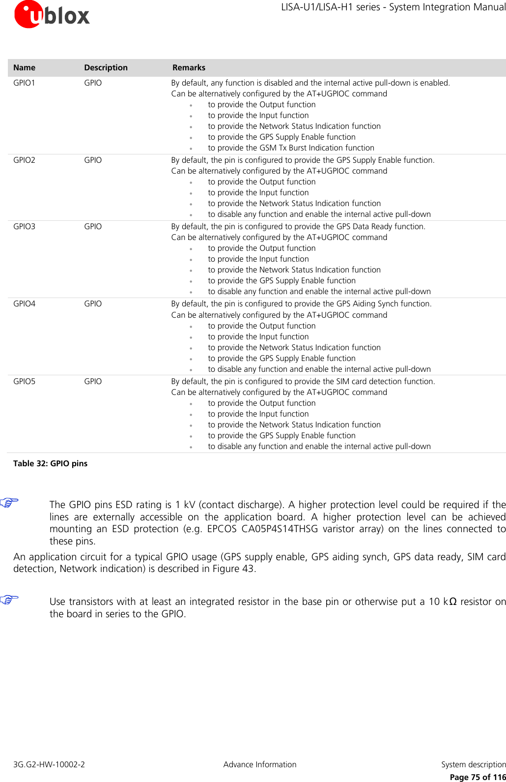
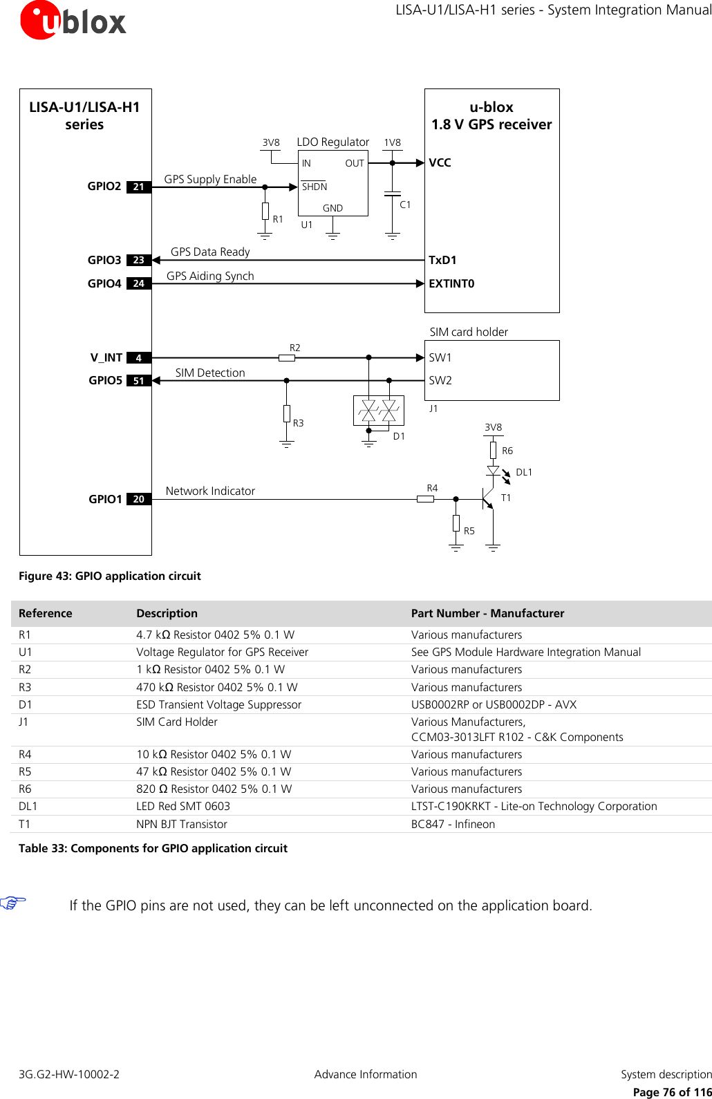
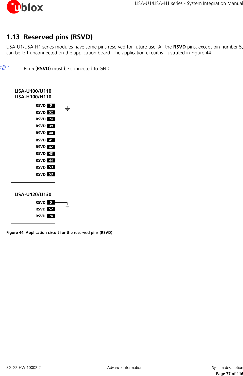
![LISA-U1/LISA-H1 series - System Integration Manual 3G.G2-HW-10002-2 Advance Information Design-In Page 82 of 116 2 Design-In 2.1 Design-in checklist This section provides a design-in checklist. 2.1.1 Schematic checklist The following are the most important points for a simple schematic check: DC supply must provide a nominal voltage at VCC pin above the minimum operating range limit. DC supply must be capable of providing 2.5 A current pulses, providing a voltage at VCC pin above the minimum operating range limit and with a maximum 400 mV voltage drop from the nominal value. VCC supply should be clean, with very low ripple/noise: suggested passive filtering parts can be inserted. VCC voltage must ramp from 2.5 V to 3.2 V within 1 ms to allow a proper switch-on of the module. Connect only one DC supply to VCC: different DC supply systems are mutually exclusive. Do not leave PWR_ON floating: add a pull-up resistor to V_BCKP. Don’t apply loads which might exceed the limit for maximum available current from V_INT supply. Check that voltage level of any connected pin does not exceed the relative operating range. Capacitance and series resistance must be limited on each SIM signal to match the SIM specifications. Insert the suggested low capacitance ESD protection and passive filtering parts on each SIM signal. Check UART signals direction, since the signal names follow the ITU-T V.24 Recommendation [3]. Provide appropriate access to USB interface and/or to UART RxD, TxD lines and access to PWR_ON and/or RESET_N lines on the application board in order to flash/upgrade the module firmware. Provide appropriate access to USB interface and/or to UART RxD, TxD, CTS, RTS lines for debugging. Add a proper pull-up resistor to a proper supply on each DDC (I2C) interface line, if the interface is used. Capacitance and series resistance must be limited on each line of the DDC interface. Use transistors with at least an integrated resistor in the base pin or otherwise put a 10 kΩ resistor on the board in series to the GPIO when those are used to drive LEDs. Connect the pin number 5 (RSVD) to ground. Insert the suggested passive filtering parts on each used analog audio line. Check the digital audio interface specifications to connect a proper device. Provide proper precautions for ESD immunity as required on the application board. All unused pins can be left floating on the application board except the PWR_ON pin (must be connected to V_BCKP by a pull-up resistor) and the RSVD pin number 5 (must be connected to GND). 2.1.2 Layout checklist The following are the most important points for a simple layout check: Check 50 nominal characteristic impedance of the RF transmission line connected to ANT pad. Follow the recommendations of the antenna producer for correct antenna installation and deployment (PCB layout and matching circuitry). Ensure no coupling occurs with other noisy or sensitive signals (primarily MIC signals, audio output signals, SIM signals). VCC line should be wide and short. Route VCC supply line away from sensitive analog signals.](https://usermanual.wiki/u-blox/LISAU120/User-Guide-1470694-Page-82.png)
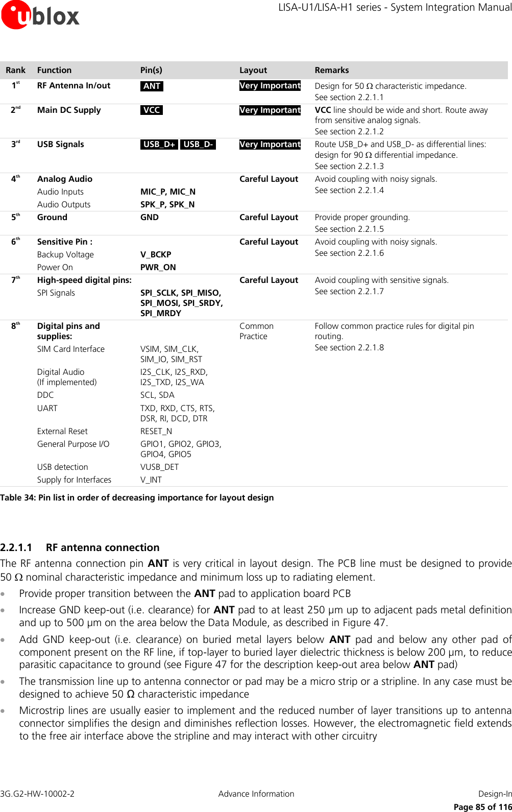
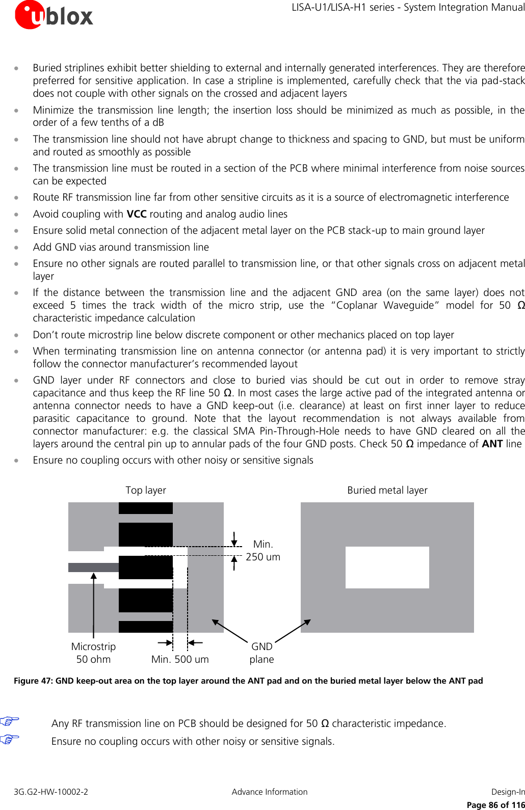
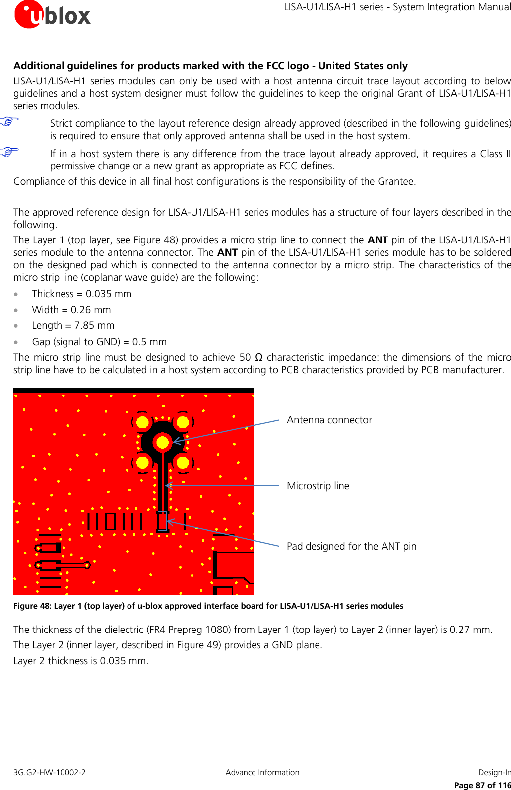
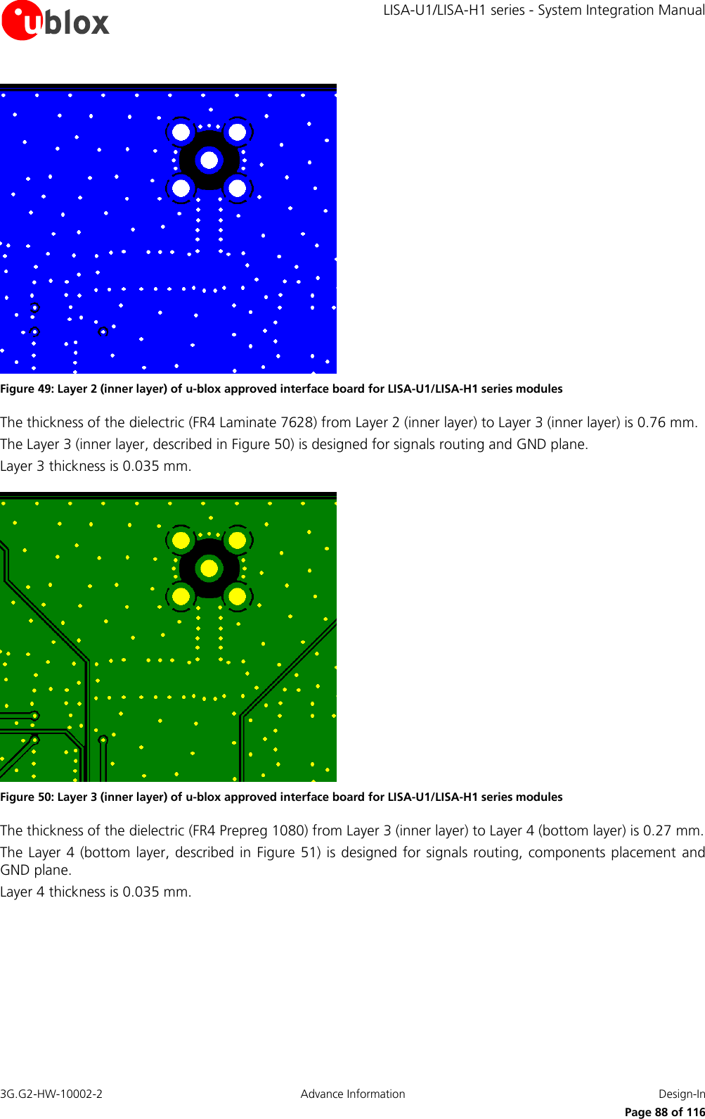
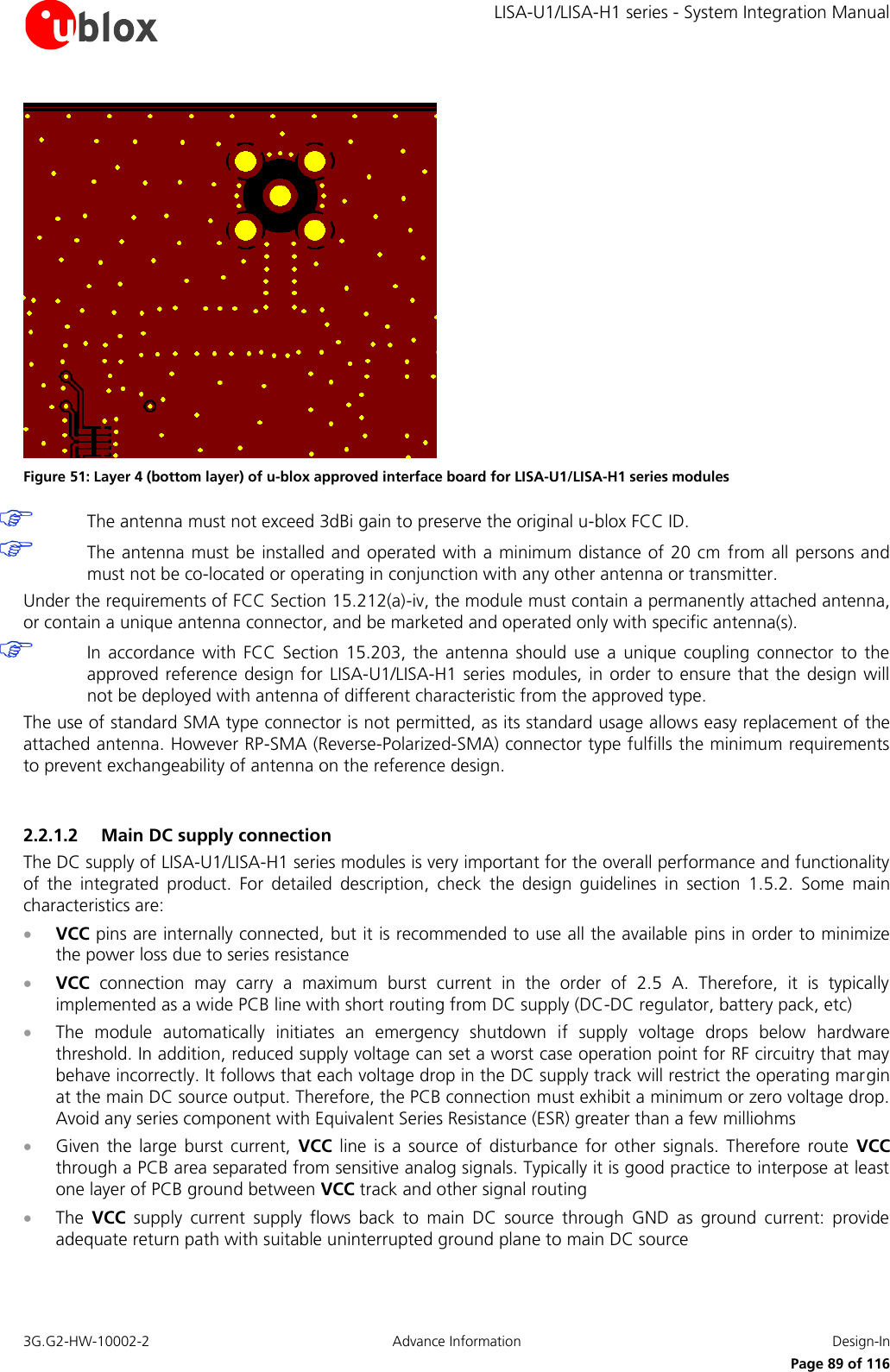
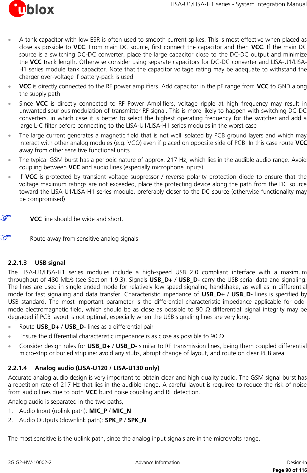
![LISA-U1/LISA-H1 series - System Integration Manual 3G.G2-HW-10002-2 Advance Information Design-In Page 93 of 116 2.2.2 Footprint and paste mask The following figure describes the footprint and provides recommendations for the paste mask for LISA-U1/LISA-H1 series modules. These are recommendations only and not specifications. Note that the copper and solder masks have the same size and position. 33.2 mm [1307.1 mil] 22.4 mm [881.9 mil]2.3 mm [90.6 mil]0.8 mm [31.5 mil]1.1 mm [43.3 mil]0.8 mm [31.5 mil]1.0 mm [39.3 mil]5.7 mm [224.4 mil]33.2 mm [1307.1 mil] 22.4 mm [881.9 mil]2.3 mm [90.6 mil]1.2 mm [47.2 mil]1.1 mm [43.3 mil]0.8 mm [31.5 mil]0.9 mm [35.4 mil]5.7 mm [224.4 mil]0.6 mm [23.6 mil]Stencil: 120 µm Figure 52: LISA-U1/LISA-H1 series modules suggested footprint and paste mask To improve the wetting of the half vias, reduce the amount of solder paste under the module and increase the volume outside of the module by defining the dimensions of the paste mask to form a T-shape (or equivalent) extending beyond the copper mask. The solder paste should have a total thickness of 120 µm. The paste mask outline needs to be considered when defining the minimal distance to the next component. The exact geometry, distances, stencil thicknesses and solder paste volumes must be adapted to the specific production processes (e.g. soldering etc.) of the customer. The bottom layer of LISA-U1/LISA-H1 series modules shows an unprotected copper area for GND described in Figure 53. Consider “No-routing” area for the LISA-U1/LISA-H1 series modules footprint as follows: signals keep-out area on the top layer of the application board, below LISA-U1/LISA-H1 series modules, due to GND opening on module bottom layer (see Figure 53).](https://usermanual.wiki/u-blox/LISAU120/User-Guide-1470694-Page-93.png)
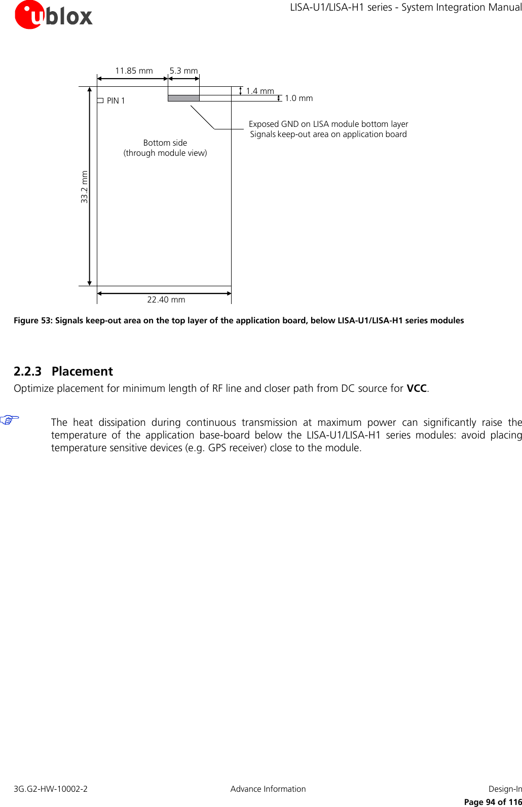
![LISA-U1/LISA-H1 series - System Integration Manual 3G.G2-HW-10002-2 Advance Information Design-In Page 95 of 116 2.3 Thermal aspects The operating temperature range is specified in the LISA-U1/LISA-H1 series Data Sheet [1]. The most critical condition concerning thermal performance is the uplink transmission at maximum power (data upload or voice call in connected mode), when the baseband processor runs at full speed, radio circuits are all active and the RF power amplifier is driven to higher output RF power. This scenario is not often encountered in real networks; however the application should be correctly designed to cope with it. During transmission at maximum RF power the LISA-U1/LISA-H1 series modules generate thermal power that can exceed 2 W: this is an indicative level since the exact generated power strictly depends on operating condition such as the number of allocated TX slot and modulation (GMSK or 8PSK) or data rate (WCDMA), transmitting frequency band, etc. The generated thermal power must be adequately dissipated through the thermal and mechanical design of the application. The increase of thermal dissipation, i.e. reducing the thermal resistance, will reduce the operating temperature for internal circuitry of LISA-U1/LISA-H1 series modules for the same operating ambient temperature. This improves the device long-term reliability for applications operating at high ambient temperature. A few techniques may be used to reduce the thermal resistance in the application: Forced ventilation air-flow within mechanical enclosure Usage of thermal transfer material (e.g. greases and pastes) Heat sink attached to the module top side, with electrically insulated / high thermal conductivity adhesive Connect each GND pin with solid ground layer of the application board and connect each ground area of the multilayer application board with complete via stack down to main ground layer](https://usermanual.wiki/u-blox/LISAU120/User-Guide-1470694-Page-95.png)
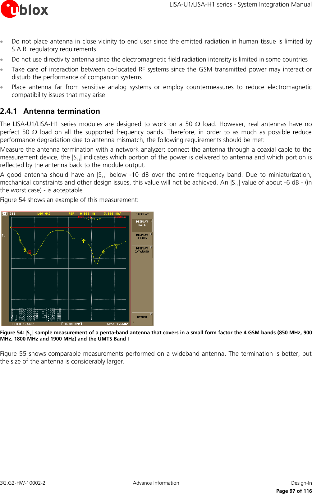
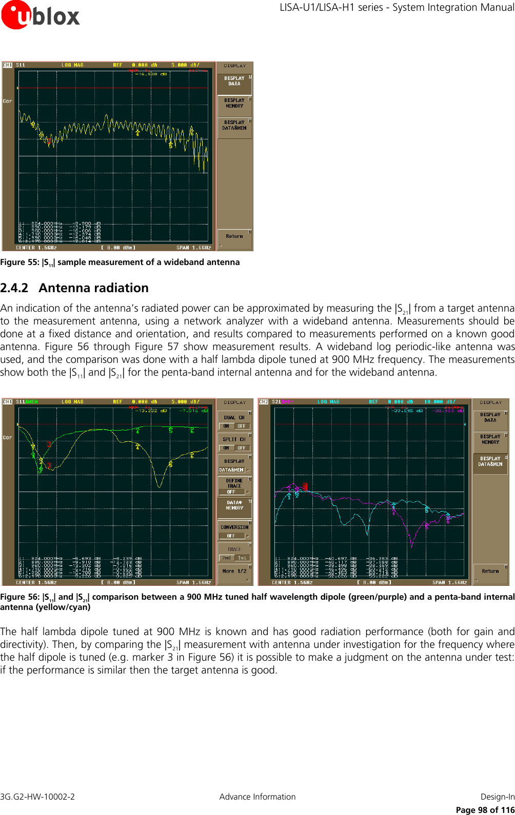
![LISA-U1/LISA-H1 series - System Integration Manual 3G.G2-HW-10002-2 Advance Information Design-In Page 99 of 116 Figure 57: |S11| and |S21| comparison between a 900 MHz tuned half wavelength dipole (green/purple) and a wideband commercial antenna (yellow/cyan) Instead if |S21| values for the tuned dipole are much better than the antenna under evaluation (like for marker 1/2 area of Figure 57, where dipole is 5 dB better), then it can be argued that the radiation of the target antenna (the wideband dipole in this case) is considerably less. The same procedure should be repeated on other bands with half wavelength dipole re-tuned to the band under investigation. For good antenna radiation performance, antenna dimensions should be comparable to a quarter of the wavelength. Different antenna types can be used for the module, many of them (e.g. patch antennas, monopole) are based on a resonating element that works in combination with a ground plane. The ground plane, ideally infinite, can be reduced down to a minimum size that must be similar to one quarter of the wavelength of the minimum frequency that has to be radiated (transmitted/received). Numerical sample: frequency = 1 GHz wavelength = 30 cm minimum ground plane (or antenna size) = 7.5 cm. Below this size, the antenna efficiency is reduced. 2.4.3 Antenna detection functionality The internal antenna detect circuit is based on ADC measurement at ANT: the RF port is DC coupled to the ADC unit in the baseband chip which injects a DC current (10 µA for 128 µs) on ANT and measures the resulting DC voltage to evaluate the resistance from ANT pad to GND. The antenna detection is forced by the +UANTR AT command: refer to the u-blox AT Commands Manual [2] for more details on how to access this feature. To achieve antenna detection functionality, use an RF antenna with built-in resistor from ANT signal to GND, or implement an equivalent solution with a circuit between the antenna cable connection and the radiating element as shown in Figure 58.](https://usermanual.wiki/u-blox/LISAU120/User-Guide-1470694-Page-99.png)

![LISA-U1/LISA-H1 series - System Integration Manual 3G.G2-HW-10002-2 Advance Information Design-In Page 101 of 116 Reported values close to the used diagnostic resistor nominal value (i.e. values from 13 kΩ to 17 kΩ if a 15 kΩ diagnostic resistor is used) indicate that the antenna is properly connected Values close to the measurement range maximum limit (approximately 50 kΩ) or an open-circuit “over range” report (see u-blox AT Commands Manual [2]) means that that the antenna is not connected or the RF cable is broken Reported values below the measurement range minimum limit (1 kΩ) will highlight a short to GND at antenna or along the RF cable Measurement inside the valid measurement range and outside the expected range may indicate an improper connection, damaged antenna or wrong value of antenna load resistor for diagnostic Reported value could differ from the real resistance value of the diagnostic resistor mounted inside the antenna assembly due to antenna cable length, antenna cable capacity and the used measurement method](https://usermanual.wiki/u-blox/LISAU120/User-Guide-1470694-Page-101.png)
![LISA-U1/LISA-H1 series - System Integration Manual 3G.G2-HW-10002-2 Advance Information Design-In Page 102 of 116 2.5 ESD immunity test precautions The immunity to the EMS phenomenon Electrostatic Discharge of the device (i.e. the application board where the LISA-U1/LISA-H1 series module is mounted) must be certified complying the testing requirements standard [10] and the requirements for radio and digital cellular radio telecommunications system equipments standards [11] [12]. The ESD test is performed at the enclosure port [11] referred as the physical boundary through which EM field radiates. If the device implements an integral antenna [11] the enclosure is intended as all insulating surfaces housing the device. If the device implements a removable antenna [11] the enclosure port is limited to the antenna port [11] hence the enclosure port comprises the antenna element and its interconnecting cable surfaces. The applicability of the ESD test depends to the device classification [11], as well the test on other ports [11] or on interconnecting cables to auxiliary equipments depends to the device accessible interfaces and manufacturer requirements. Contact discharges [10] are performed at conductive surfaces whereas air discharges [10] are performed at insulating surfaces. Indirect contact discharges are performed on the measurement setup horizontal and vertical coupling planes [10]. Some precautions should be implemented as described in the following sections in order to satisfy ESD immunity test requirements [10] [11] [12] performed at device enclosure complying the category level [11] and shown in the following table. Category Immunity Level Contact Discharge to coupling planes (indirect contact discharge) +2 kV / -2 kV +4 kV / -4 kV Contact Discharges to conducted surfaces (direct contact discharge) Not Applicable2* Air Discharge at insulating surfaces +2 kV / -2 kV +4 kV / -4 kV +8 kV / -8 kV Table 37: Enclosure ESD immunity level, standards “EN 61000-4-2, EN 301 489-1 V1.8.1, EN 301 489-7 V1.3.1” 2.5.1 General precautions The following module interfaces could be involved in the ESD immunity test criticality depending on the application board handling. Some precautions are herein suggested. Sensitive interface is the reset line (RESET_N pin): A 47 pF bypass capacitor (e.g. Murata GRM1555C1H470JA01) have to be mounted on the line termination connected to the RESET_N pin to avoid a module reset caused by an electrostatic discharge applied to the application board A series ferrite bead (e.g. Murata BLM15HD182SN1) must be added on the line connected to the RESET_N pin to avoid a module reset caused by an electrostatic discharge applied to the application board 2 LISA mounted on application reference design: Applicability -> EUT with insulating surfaces, air discharges on interconnecting cables between EUT and antenna and auxiliary equipments Not Applicability -> EUT with conductive surface, direct contact discharge](https://usermanual.wiki/u-blox/LISAU120/User-Guide-1470694-Page-102.png)
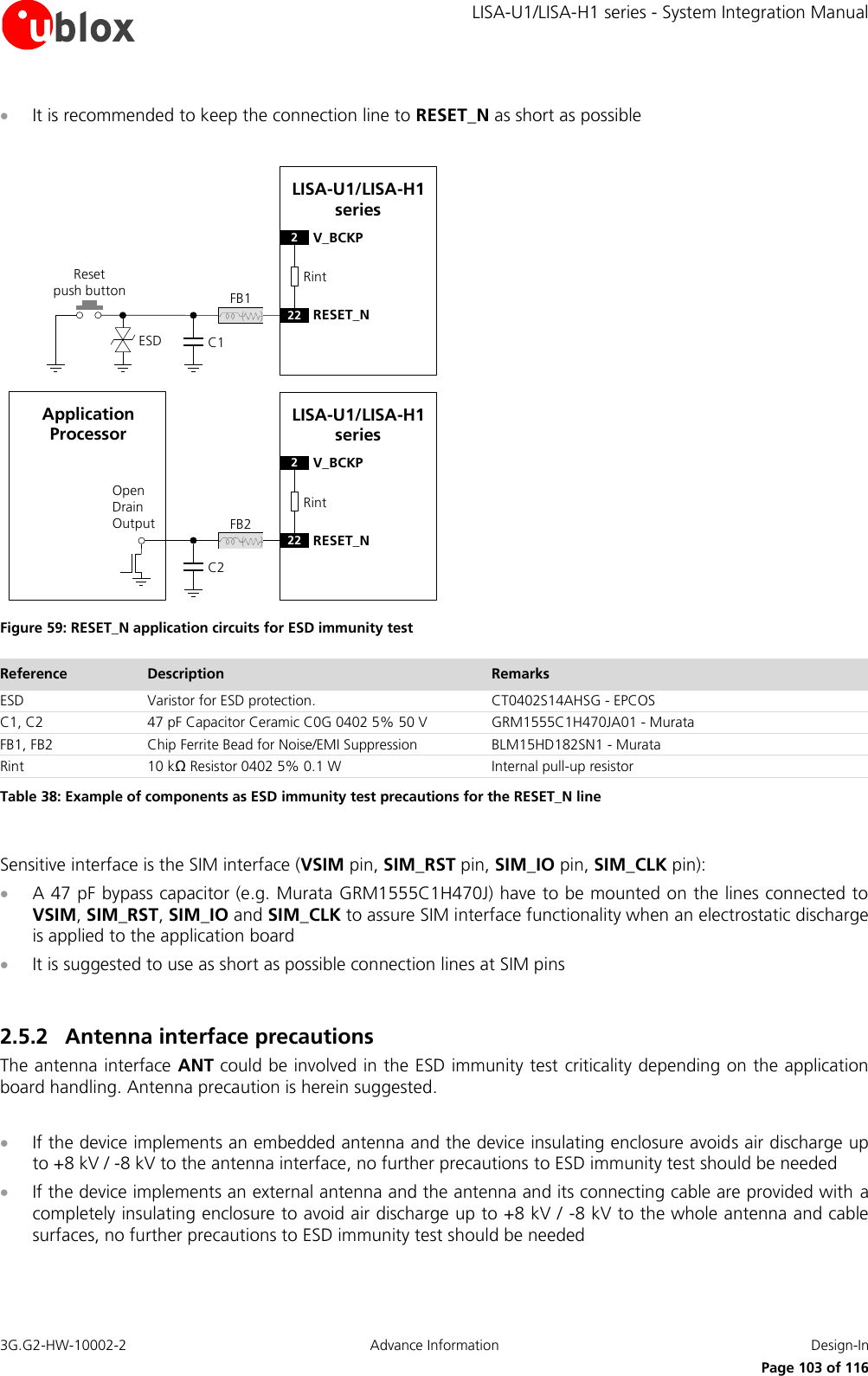
![LISA-U1/LISA-H1 series - System Integration Manual 3G.G2-HW-10002-2 Advance Information Design-In Page 104 of 116 If the device implements an external antenna and the antenna or its connecting cable are not provided with completely insulating enclosure to avoid air discharge up to +8 kV / -8 kV to the whole antenna and cable surfaces, precautions to ESD immunity test should be implemented on the application board A higher protection level is required at the ANT port if the line is externally accessible on the application board. 2.5.3 Module interfaces precautions All the module pins that are externally accessible should be included in the ESD immunity test since they are considered to be a port [11]. Depending on applicability, and in order to satisfy ESD immunity test requirements and ESD category level, pins connected to the port should be protected up to +4 kV / -4 kV for direct Contact Discharge, and up to +8 kV / -8 kV for Air Discharge applied to the enclosure. The maximum ESD rating of all the pins of the module, except the ANT pin, is 1 kV (HBM according MIL-Std 883D, method 3015.7, EOS/ESD Standard S5.1-1993). A higher protection level can be achieved by mounting an ESD protection (e.g. EPCOS CA05P4S14THSG varistor array).](https://usermanual.wiki/u-blox/LISAU120/User-Guide-1470694-Page-104.png)
![LISA-U1/LISA-H1 series - System Integration Manual 3G.G2-HW-10002-2 Advance Information Handling and soldering Page 105 of 116 3 Handling and soldering No natural rubbers, no hygroscopic materials or materials containing asbestos are employed. 3.1 Packaging, shipping, storage and moisture preconditioning For information pertaining to reels and tapes, Moisture Sensitivity levels (MSD), shipment and storage information, as well as drying for preconditioning see the LISA-U1/LISA-H1 series Data Sheet [1]. The LISA-U1/LISA-H1 series modules are Electro-Static Discharge (ESD) sensitive devices. Ensure ESD precautions are implemented during handling of the module. 3.2 Soldering 3.2.1 Soldering paste Use of "No Clean" soldering paste is strongly recommended, as it does not require cleaning after the soldering process has taken place. The paste listed in the example below meets these criteria. Soldering Paste: OM338 SAC405 / Nr.143714 (Cookson Electronics) Alloy specification: 95.5% Sn / 3.9% Ag / 0.6% Cu (95.5% Tin / 3.9% Silver / 0.6% Copper) 95.5% Sn / 4.0% Ag / 0.5% Cu (95.5% Tin / 4.0% Silver / 0.5% Copper) Melting Temperature: 217°C Stencil Thickness: 120 µm for base boards The final choice of the soldering paste depends on the approved manufacturing procedures. The paste-mask geometry for applying soldering paste should meet the recommendations in section 2.2.2 The quality of the solder joints on the connectors (’half vias’) should meet the appropriate IPC specification. 3.2.2 Reflow soldering A convection type-soldering oven is strongly recommended over the infrared type radiation oven. Convection heated ovens allow precise control of the temperature and all parts will be heated up evenly, regardless of material properties, thickness of components and surface color. Consider the "IPC-7530 Guidelines for temperature profiling for mass soldering (reflow and wave) processes, published 2001". Preheat phase Initial heating of component leads and balls. Residual humidity will be dried out. Please note that this preheat phase will not replace prior baking procedures. Temperature rise rate: max 3°C/s If the temperature rise is too rapid in the preheat phase it may cause excessive slumping. Time: 60 – 120 s If the preheat is insufficient, rather large solder balls tend to be generated. Conversely, if performed excessively, fine balls and large balls will be generated in clusters.](https://usermanual.wiki/u-blox/LISAU120/User-Guide-1470694-Page-105.png)
![LISA-U1/LISA-H1 series - System Integration Manual 3G.G2-HW-10002-2 Advance Information Handling and soldering Page 106 of 116 End Temperature: 150 - 200°C If the temperature is too low, non-melting tends to be caused in areas containing large heat capacity. Heating/ reflow phase The temperature rises above the liquidus temperature of 217°C. Avoid a sudden rise in temperature as the slump of the paste could become worse. Limit time above 217°C liquidus temperature: 40 - 60 s Peak reflow temperature: 245°C Cooling phase A controlled cooling avoids negative metallurgical effects (solder becomes more brittle) of the solder and possible mechanical tensions in the products. Controlled cooling helps to achieve bright solder fillets with a good shape and low contact angle. Temperature fall rate: max 4°C / s To avoid falling off, modules should be placed on the topside of the motherboard during soldering. The final soldering temperature chosen at the factory depends on additional external factors like choice of soldering paste, size, thickness and properties of the base board, etc. Exceeding the maximum soldering temperature in the recommended soldering profile may permanently damage the module. Preheat Heating Cooling[°C] Peak Temp. 245°C [°C]250 250Liquidus Temperature217 217200 20040 - 60 sEnd Temp.max 4°C/s150 - 200°C150 150max 3°C/s60 - 120 s100 Typical Leadfree 100Soldering Profile50 50050 100 150 200 250 300Elapsed time [s] Figure 60: Recommended soldering profile When soldering lead-free LISA-U1/LISA-H1 series modules in a leaded process, check the following temperatures: PB- Technology Soaktime: 40-80 s Time above Liquidus: 40-90 s Peak temperature: 225-235°C LISA-U1/LISA-H1 series modules must not be soldered with a damp heat process.](https://usermanual.wiki/u-blox/LISAU120/User-Guide-1470694-Page-106.png)

![LISA-U1/LISA-H1 series - System Integration Manual 3G.G2-HW-10002-2 Advance Information Appendix Page 110 of 116 Appendix A Extra Features A.1 TCP/IP Via the AT commands it’s possible to access the TCP/IP functionalities over the GPRS connection. For more details about AT commands see the u-blox AT Commands Manual [2]. A.1.1 Multiple IP addresses and sockets Using LISA’s embedded TCP/IP or UDP/IP stack, only 1 IP instance (address) is supported. The IP instance supports up to 16 sockets. Using an external TCP/IP stack (on the application processor), it is possible to have 2 IP instances (addresses). A.2 FTP LISA-U1/LISA-H1 series modules will support this feature in the upcoming version. A.3 FTPS LISA-U1/LISA-H1 series modules will support this feature in the upcoming version. A.4 HTTP LISA-U1/LISA-H1 series modules will support this feature in the upcoming version. A.5 HTTPS LISA-U1/LISA-H1 series modules will support this feature in the upcoming version. A.6 SMTP LISA-U1/LISA-H1 series modules will support this feature in the upcoming version. A.7 AssistNow clients and GPS integration For customers using u-blox GPS receivers, LISA-U1/LISA-H1 series modules feature embedded AssistNow Online and AssistNow Offline clients. AssistNow A-GPS provides better GPS performance and faster Time-To-First-Fix. The clients can be enabled / disabled with an AT command. LISA-U1/LISA-H1 series modules act as a stand-alone AssistNow client, making AssistNow available with no additional requirements for resources or software integration on an external host micro controller. Full access to u-blox GPS receivers is available via the LISA-U1/LISA-H1 series, through a dedicated DDC (I2C) interface, while the available GPIOs can handle the GPS device power on/off. This means that GSM/EDGE and GPS can be controlled through a single serial port from any host processor. A.8 In-Band modem (LISA-U130 only) LISA-U130 Automotive grade version implements the in-Band modem solution for eCall according to the 3GPP TS 26.267 specification [13]. According to the eCall (Pan-European automatic in-vehicle emergency call system) specification, an eCall must be generated automatically or manually following an car accident using GSM cellular service “112”. When activated, the in-vehicle eCall system (IVS) creates an emergency call carrying both voice and data (e.g. vehicle GPS position) directly to the nearest 112 Public Safety Answering Point (PSAP) to quickly decide upon detaching rescue services to the known position.](https://usermanual.wiki/u-blox/LISAU120/User-Guide-1470694-Page-110.png)
![LISA-U1/LISA-H1 series - System Integration Manual 3G.G2-HW-10002-2 Advance Information Appendix Page 111 of 116 Figure 62: In-Band modem diagram flow In-band modem allows the fast and reliable transmission of vehicle Minimum Set of Data (MSD - 140 bytes) and the establishment of a voice emergency call using the same physical channel (voice channel) without any modifications of the existing cellular network architecture. In-Band modem is a mandatory feature to meet the eCall requirements and to develop in vehicle devices fully supporting eCall. The in-Band modem functionality is delivered upon request. A.9 Smart temperature supervision An internal sensor is used to constantly monitor the board temperature of the LISA-U1/LISA-H1 series modules. The measured value is compared with the internally predefined thresholds and it proceeds accordingly. A warning notification is reported by the module when the temperature value is still inside the valid range (i.e. the module is still in a valid and good working condition) but it is close to the limit (upper or lower). A shutdown is notified and automatically forced by the module when the temperature value is outside the specified range (i.e. the module is in a dangerous working condition). For security reasons the shutdown is suspended in case of emergency call in progress: in this case the device will switch off at call termination. The Smart Temperature Supervisor feature can be enabled or disabled through an AT command (for more details please to u-blox AT commands manual [2], +USTS AT command). If the feature is disabled there is no embedded protection against not allowed temperature working conditions. The sensor measures board temperature inside the shields, which can differ from ambient temperature.](https://usermanual.wiki/u-blox/LISAU120/User-Guide-1470694-Page-111.png)

![LISA-U1/LISA-H1 series - System Integration Manual 3G.G2-HW-10002-2 Advance Information Related documents Page 114 of 116 Related documents [1] u-blox LISA-U1/LISA-H1 series Data Sheet, Docu No 3G.G1-HW-10001 [2] u-blox AT Commands Manual, Docu No WLS-SW-11000 [3] ITU-T Recommendation V.24, 02-2000. List of definitions for interchange circuits between data terminal equipment (DTE) and data circuit-terminating equipment (DCE). http://www.itu.int/rec/T-REC-V.24-200002-I/en [4] 3GPP TS 27.007 - AT command set for User Equipment (UE) (Release 1999) [5] 3GPP TS 27.005 - Use of Data Terminal Equipment - Data Circuit terminating; Equipment (DTE - DCE) interface for Short Message Service (SMS) and Cell Broadcast Service (CBS) (Release 1999) [6] 3GPP TS 27.010 - Terminal Equipment to User Equipment (TE-UE) multiplexer protocol (Release 1999) [7] Universal Serial Bus Revision 2.0 specification, http://www.usb.org/developers/docs/ [8] I2C-Bus Specification Version 2.1 Philips Semiconductors (January 2000), http://www.nxp.com/acrobat_download/literature/9398/39340011_21.pdf [9] RFC3267 - Real-Time Transport Protocol (RTP) Payload Format and File Storage, Format for the Adaptive Multi-Rate (AMR) and Adaptive Multi-Rate Wideband (AMR-WB) Audio Codecs [10] CENELEC EN 61000-4-2 (2001): "Electromagnetic compatibility (EMC) - Part 4-2: Testing and measurement techniques - Electrostatic discharge immunity test". [11] ETSI EN 301 489-1 V1.8.1: “Electromagnetic compatibility and Radio spectrum Matters (ERM); ElectroMagnetic Compatibility (EMC) standard for radio equipment and services; Part 1: Common technical requirements” [12] ETSI EN 301 489-7 V1.3.1 “Electromagnetic compatibility and Radio spectrum Matters (ERM); ElectroMagnetic Compatibility (EMC) standard for radio equipment and services; Part 7: Specific conditions for mobile and portable radio and ancillary equipment of digital cellular radio telecommunications systems (GSM and DCS)“ [13] 3GPP TS 26.267 - Technical Specification Group Services and System Aspects; eCall Data Transfer; In-band modem solution; General description (Release 9) [15] GSM Mux Implementation Application Note, Docu No WLS-CS-11002 [17] Firmware Update Application Note, Docu No WLS-CS-11001 [18] SPI Interface application Note, Docu No 3G.G2-CS-11000 Some of the above documents can be downloaded from u-blox web-site (http://www.u-blox.com). Revision history Revision Date Name Status / Comments - 21/10/2010 sses Initial Release 1 11/01/2011 sses Thickness information added GPIO description improved 2 26/04/2011 lpah Update to Advance Information status and paste mask](https://usermanual.wiki/u-blox/LISAU120/User-Guide-1470694-Page-114.png)