u blox LISAU120 LISA-U120 User Manual LISA U1 LISA H1 series
u-blox AG LISA-U120 LISA U1 LISA H1 series
u blox >
[short-term confidential] User's Manual
LISA-U1/LISA-H1 series
3.75G/3.5G HSxPA
Wireless Modules
System Integration Manual
Abstract
This document describes the features and the integration of the
LISA-U1/LISA-H1 series HSxPA wireless modules.
LISA-U1/LISA-H1 series modules are a complete and cost efficient
3.75G/3.5G solution offering high-speed dual-band HSDPA/HSUPA
and quad-band GSM/GPRS voice and/or data transmission
technology in a compact form factor.
locate, communicate, accelerate
33.2 x 22.4 x 2.7 mm
www.u-blox.com
LISA-U1/LISA-H1 series - System Integration Manual
3G.G2-HW-10002-2 Page 2 of 116
Document Information
Title
LISA-U1/LISA-H1 series
Subtitle
3.75G/3.5G HSxPA
Wireless Modules
Document type
System Integration Manual
Document number
3G.G2-HW-10002-2
Document status
Advance Information
Document status information
Objective
Specification
This document contains target values. Revised and supplementary data will be published
later.
Advance
Information
This document contains data based on early testing. Revised and supplementary data will
be published later.
Preliminary
This document contains data from product verification. Revised and supplementary data
may be published later.
Released
This document contains the final product specification.
This document applies to the following products:
Name
Type number
Firmware version
PCN / IN
LISA-U100
LISA-U100-00S-00
n.a.
n.a.
LISA-U110
LISA-U110-00S-00
n.a.
n.a.
LISA-U120
LISA-U120-00S-00
n.a.
n.a.
LISA-U130
LISA-U130-00S-00
n.a.
n.a.
LISA-H100
LISA-H100-00S-00
n.a.
n.a.
LISA-H110
LISA-H110-00S-00
n.a.
n.a.
This document and the use of any information contained therein, is subject to the acceptance of the u-blox terms and conditions. They
can be downloaded from www.u-blox.com.
u-blox makes no warranties based on the accuracy or completeness of the contents of this document and reserves the right to make
changes to specifications and product descriptions at any time without notice.
u-blox reserves all rights to this document and the information contained herein. Reproduction, use or disclosure to third parties without
express permission is strictly prohibited. Copyright © 2011, u-blox AG.
u-blox® is a registered trademark of u-blox Holding AG in the EU and other countries.

LISA-U1/LISA-H1 series - System Integration Manual
3G.G2-HW-10002-2 Advance Information Preface
Page 3 of 116
Preface
u-blox Technical Documentation
As part of our commitment to customer support, u-blox maintains an extensive volume of technical
documentation for our products. In addition to our product-specific technical data sheets, the following manuals
are available to assist u-blox customers in product design and development.
AT Commands Manual: This document provides the description of the supported AT commands by the
LISA-U1/LISA-H1 series module to verify all implemented functionalities.
System Integration Manual: This Manual provides hardware design instructions and information on how to
set up production and final product tests.
Application Note: document provides general design instructions and information that applies to all u-blox
Wireless modules. See Section Related documents for a list of Application Notes related to your Wireless
Module.
How to use this Manual
The LISA-U1/LISA-H1 series System Integration Manual provides the necessary information to successfully design
in and configure these u-blox wireless modules.
This manual has a modular structure. It is not necessary to read it from the beginning to the end.
The following symbols are used to highlight important information within the manual:
An index finger points out key information pertaining to module integration and performance.
A warning symbol indicates actions that could negatively impact or damage the module.
Questions
If you have any questions about u-blox Wireless Integration, please:
Read this manual carefully.
Contact our information service on the homepage http://www.u-blox.com
Read the questions and answers on our FAQ database on the homepage http://www.u-blox.com
Technical Support
Worldwide Web
Our website (www.u-blox.com) is a rich pool of information. Product information, technical documents and
helpful FAQ can be accessed 24h a day.
By E-mail
Contact the nearest of the Technical Support offices by email. Use our service pool email addresses rather than
any personal email address of our staff. This makes sure that your request is processed as soon as possible. You
will find the contact details at the end of the document.
Helpful Information when Contacting Technical Support
When contacting Technical Support please have the following information ready:
Module type (e.g. LISA-U100) and firmware version
Module configuration
Clear description of your question or the problem
A short description of the application
Your complete contact details

LISA-U1/LISA-H1 series - System Integration Manual
3G.G2-HW-10002-2 Advance Information Contents
Page 4 of 116
Contents
Preface ................................................................................................................................ 3
Contents .............................................................................................................................. 4
1 System description ....................................................................................................... 7
1.1 Overview .............................................................................................................................................. 7
1.2 Architecture .......................................................................................................................................... 8
1.2.1 Functional blocks ........................................................................................................................... 9
1.2.2 Hardware differences between LISA-U1/LISA-H1 series modules .................................................. 10
1.3 Pin-out ............................................................................................................................................... 11
1.4 Operating modes ................................................................................................................................ 14
1.5 Power management ........................................................................................................................... 16
1.5.1 Power supply circuit overview ...................................................................................................... 16
1.5.2 Module supply (VCC) .................................................................................................................. 17
1.5.3 Current consumption profiles ...................................................................................................... 24
1.5.4 RTC Supply (V_BCKP) .................................................................................................................. 28
1.5.5 Interface supply (V_INT) ............................................................................................................... 30
1.6 System functions ................................................................................................................................ 31
1.6.1 Module power on ....................................................................................................................... 31
1.6.2 Module power off ....................................................................................................................... 35
1.6.3 Module reset ............................................................................................................................... 36
1.7 RF connection ..................................................................................................................................... 37
1.8 (U)SIM interface .................................................................................................................................. 38
1.8.1 (U)SIM functionality ..................................................................................................................... 40
1.9 Serial communication ......................................................................................................................... 41
1.9.1 Serial interfaces configuration ..................................................................................................... 41
1.9.2 Asynchronous serial interface (UART)........................................................................................... 42
1.9.3 USB interface............................................................................................................................... 54
1.9.4 SPI interface ................................................................................................................................ 56
1.9.5 MUX Protocol (3GPP 27.010) ...................................................................................................... 60
1.10 DDC (I2C) interface .......................................................................................................................... 61
1.10.1 Overview ..................................................................................................................................... 61
1.10.2 DDC application circuit ................................................................................................................ 62
1.11 Audio Interface (LISA-U120 and LISA-U130 only) ............................................................................ 63
1.11.1 Analog Audio interface ............................................................................................................... 64
1.11.2 Digital Audio interface ................................................................................................................. 70
1.11.3 Voiceband processing system ...................................................................................................... 72
1.12 General Purpose Input/Output (GPIO) ............................................................................................. 74
1.13 Reserved pins (RSVD) ...................................................................................................................... 77
1.14 Schematic for LISA-U1/LISA-H1 series module integration ............................................................... 78
1.15 Approvals ........................................................................................................................................ 79

LISA-U1/LISA-H1 series - System Integration Manual
3G.G2-HW-10002-2 Advance Information Contents
Page 5 of 116
1.15.1 R&TTED and European Conformance CE mark ............................................................................ 79
1.15.2 IC ................................................................................................................................................ 79
1.15.3 Federal communications commission notice ................................................................................ 79
2 Design-In ..................................................................................................................... 82
2.1 Design-in checklist .............................................................................................................................. 82
2.1.1 Schematic checklist ..................................................................................................................... 82
2.1.2 Layout checklist ........................................................................................................................... 82
2.1.3 Antenna checklist ........................................................................................................................ 83
2.2 Design Guidelines for Layout .............................................................................................................. 84
2.2.1 Layout guidelines per pin function ............................................................................................... 84
2.2.2 Footprint and paste mask ............................................................................................................ 93
2.2.3 Placement ................................................................................................................................... 94
2.3 Thermal aspects .................................................................................................................................. 95
2.4 Antenna guidelines ............................................................................................................................. 96
2.4.1 Antenna termination ................................................................................................................... 97
2.4.2 Antenna radiation ....................................................................................................................... 98
2.4.3 Antenna detection functionality .................................................................................................. 99
2.5 ESD immunity test precautions ......................................................................................................... 102
2.5.1 General precautions .................................................................................................................. 102
2.5.2 Antenna interface precautions ................................................................................................... 103
2.5.3 Module interfaces precautions ................................................................................................... 104
3 Handling and soldering ........................................................................................... 105
3.1 Packaging, shipping, storage and moisture preconditioning ............................................................. 105
3.2 Soldering .......................................................................................................................................... 105
3.2.1 Soldering paste.......................................................................................................................... 105
3.2.2 Reflow soldering ....................................................................................................................... 105
3.2.3 Optical inspection ...................................................................................................................... 107
3.2.4 Cleaning .................................................................................................................................... 107
3.2.5 Repeated reflow soldering ......................................................................................................... 107
3.2.6 Wave soldering.......................................................................................................................... 107
3.2.7 Hand soldering .......................................................................................................................... 107
3.2.8 Rework ...................................................................................................................................... 107
3.2.9 Conformal coating .................................................................................................................... 107
3.2.10 Casting ...................................................................................................................................... 108
3.2.11 Grounding metal covers ............................................................................................................ 108
3.2.12 Use of ultrasonic processes ........................................................................................................ 108
4 Product Testing......................................................................................................... 109
4.1 u-blox in-series production test ......................................................................................................... 109
4.2 Test parameters for OEM manufacturer ............................................................................................ 109
Appendix ........................................................................................................................ 110

LISA-U1/LISA-H1 series - System Integration Manual
3G.G2-HW-10002-2 Advance Information Contents
Page 6 of 116
A Extra Features ........................................................................................................... 110
A.1 TCP/IP ............................................................................................................................................... 110
A.1.1 Multiple IP addresses and sockets .............................................................................................. 110
A.2 FTP ................................................................................................................................................... 110
A.3 FTPS ................................................................................................................................................. 110
A.4 HTTP ................................................................................................................................................. 110
A.5 HTTPS ............................................................................................................................................... 110
A.6 SMTP ................................................................................................................................................ 110
A.7 AssistNow clients and GPS integration .............................................................................................. 110
A.8 In-Band modem (LISA-U130 only) ..................................................................................................... 110
A.9 Smart temperature supervision ......................................................................................................... 111
B Glossary .................................................................................................................... 112
Related documents......................................................................................................... 114
Revision history .............................................................................................................. 114
Contact ............................................................................................................................ 116

LISA-U1/LISA-H1 series - System Integration Manual
3G.G2-HW-10002-2 Advance Information System description
Page 7 of 116
1 System description
1.1 Overview
The LISA-U1/LISA-H1 series is a family of SMT wireless modules featuring Leadless Chip Carrier (LCC) packaging
and integrating a full-feature 3G UMTS/HSxPA and 2G GSM/GPRS/EDGE protocol stack with A-GPS support.
UMTS/HSDPA/HSUPA characteristics:
UMTS Terrestrial Radio Access (UTRA) Frequency Division Duplex (FDD) operating mode
Dual-band support:
Band II (1900 MHz) and Band V (850 MHz) for LISA-U100, LISA-U120, LISA-H100
Band I (2100 MHz) and Band VIII (900 MHz) for LISA-U110, LISA-U130, LISA-H110
Power Class 3 (24 dBm) for WCDMA/HSDPA/HSUPA mode
HSUPA category 6, up to 7.2 Mb/s DL, 5.76 Mb/s UL (LISA-U1 series only)
HSDPA category 8, up to 7.2 Mb/s DL, 384 kb/s UL (LISA-U1 series only)
HSDPA category 6, up to 3.6 Mb/s DL, 384 kb/s UL (LISA-H1 series only)
WCDMA PS data up to 384 kb/s DL/UL
WCDMA CS data up to 64 kb/s DL/UL
GSM/GPRS/EDGE characteristics:
Quad-band support: GSM 850 MHz, E-GSM 900 MHz, DCS 1800 MHz and PCS 1900 MHz
GSM/GPRS Power Class 4 (33 dBm) for GSM/E-GSM bands
GSM/GPRS Power Class 1 (30 dBm) for DCS/PCS bands
EDGE Power Class E2 (27 dBm) for GSM/E-GSM bands
EDGE Power Class E2 (26 dBm) for DCS/PCS bands
EDGE multislot class 12
1
, coding scheme MCS1-MCS9, up to 236.8 kb/s
GPRS multislot class 121, coding scheme CS1-CS4, up to 85.6 kb/s
CSD Non-transparent / Transparent Mode, up to 9.6 kb/s
As a 3G module the LISA-U1/LISA-H1 series module is Class A User Equipment: the device can work
simultaneously in Packet Switch and Circuit Switch mode. This means that voice calls are possible while the data
connection is active without any interruption in service.
As a 2G module the LISA-U1/LISA-H1 series module is Class B Mobile Station: the device can be attached to both
GPRS and GSM services (i.e. Packet Switch and Circuit Switch mode), using one service at a time. For instance, if
during data transmission an incoming call occurs, the data connection is suspended to permit the voice
communication. Once the voice call has terminated, the data service is resumed. Network operation modes I to
III are supported, with user-definable preferred service selectable from GSM to GPRS. Optionally paging
messages for GSM calls can be monitored during GPRS data transfer in not-coordinating NOM II-III.
LISA-U1/LISA-H1 series modules implement GPRS/EGPRS class 12 for data transfer. GPRS class determines the
number of timeslots available for upload and download and thus the speed at which data can be transmitted
and received, with higher classes typically allowing faster data transfer rates. Class 12 implies a maximum of 4
slots in download (reception) and 4 slots in upload (transmission) with 5 slots in total.
The network automatically configures the number of timeslots used for reception or transmission (voice calls
take precedence over GPRS traffic). The network also automatically configures channel encoding (CS1 to MCS9).
The maximum (E)GPRS bit rate of the mobile station depends on the coding scheme and number of time slots.
Direct Link mode is supported for TCP sockets.
1
GPRS/EDGE multislot class 12 implies a maximum of 4 slots in DL (reception) and 4 slots in UL (transmission) with 5 slots in total.
LISA-U1/LISA-H1 series - System Integration Manual
3G.G2-HW-10002-2 Advance Information System description
Page 8 of 116
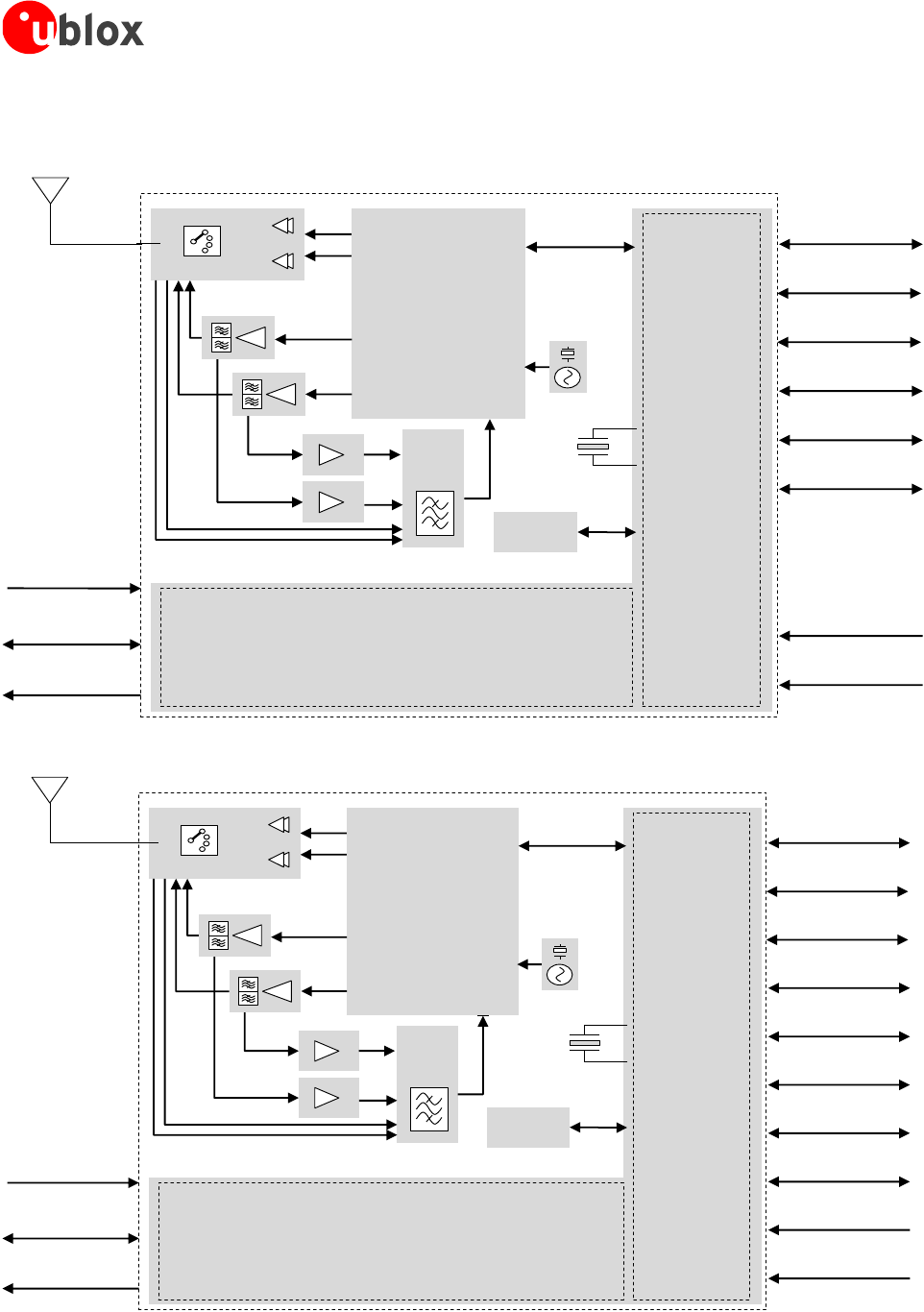
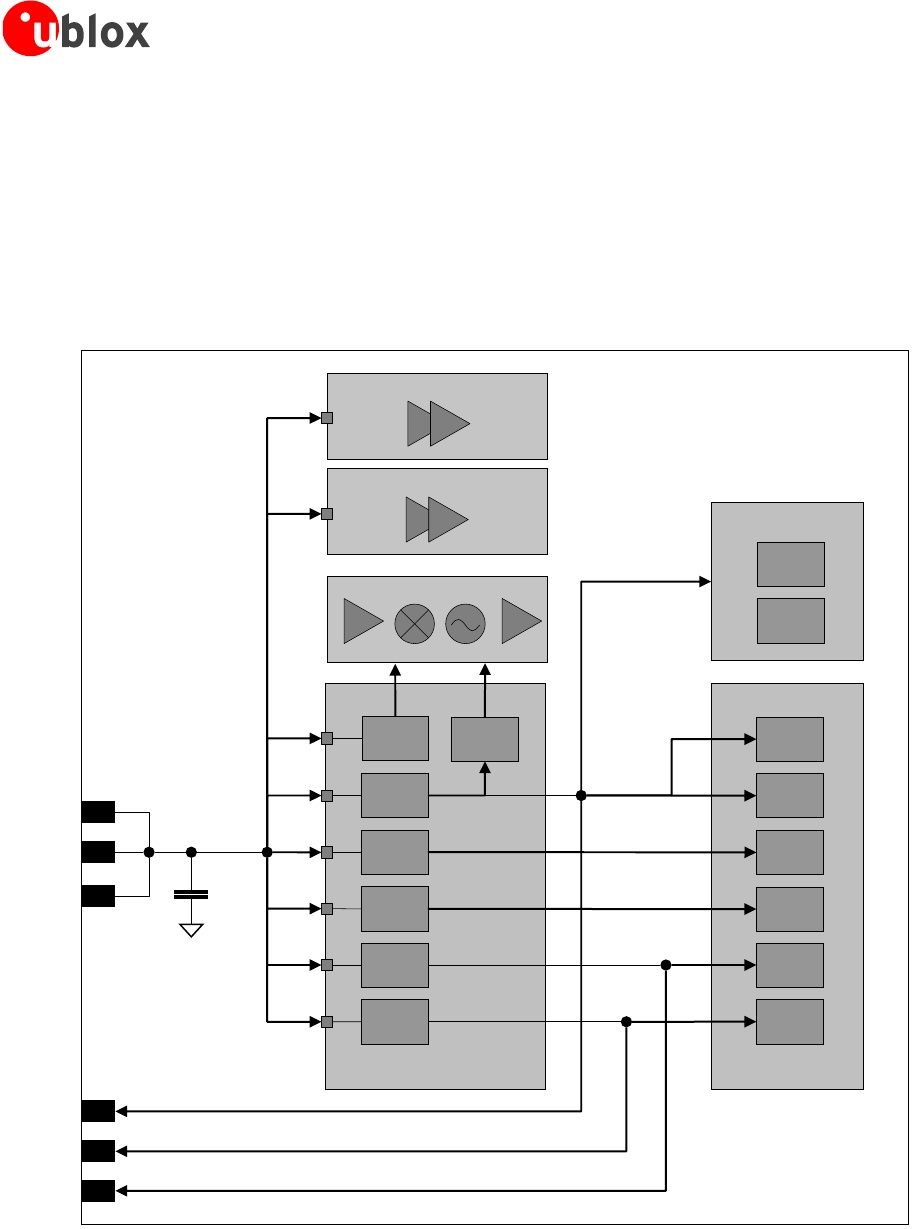
1.2 Architecture
Wireless
Base-band
Processor
Memory
Power Management Unit
RF
Transceiver
26 MHz
32.768 kHz
SAW
Filter
FEM & 2G PA
ANT
LNA
3G PA
LNA
3G PA
DDC (for GPS)
(U)SIM Card
UART
SPI
USB
GPIO(s)
Power On
External Reset
V_BCKP (RTC)
Vcc (Supply)
V_INT (I/O)
Figure 1: LISA-U100, LISA-U110, LISA-H100, LISA-H110 block diagram
Wireless
Base-band
Processor
Memory
Power Management Unit
RF
Transceiver
26 MHz
32.768 kHz
SAW
Filter
FEM & 2G PA
ANT
LNA
3G PA
LNA
3G PA
DDC (for GPS)
(U)SIM Card
UART
SPI
USB
GPIO(s)
Power On
External Reset
V_BCKP (RTC)
Vcc (Supply)
V_INT (I/O)
Digital Audio (I2S)
AnalogAudio
Figure 2: LISA-U120, LISA-U130 block diagram

LISA-U1/LISA-H1 series - System Integration Manual
3G.G2-HW-10002-2 Advance Information System description
Page 9 of 116
1.2.1 Functional blocks
LISA-U1/LISA-H1 series modules consist of the following internal functional blocks: RF high power front-end, RF
transceiver, Baseband section and Power Management Unit.
RF high-power front-end
A separated shielding box includes the RF high-power signal circuitry, namely:
Front-End Module (FEM) with integrated quad-band 2G Power Amplifier and antenna switch multiplexer
Two single-band 3G HSxPA/WCDMA Power Amplifier modules with integrated duplexers
The RF antenna is directly connected to the FEM, which dispatches the RF signals according to the active mode.
For time-duplex 2G operation, the incoming signal at the active Receiver (RX) slot is applied to integrated SAW
filters for out-of-band rejection and then sent to the appropriate receiver port of the RF transceiver. During the
allocated Transmitter (TX) slots, the low level signal coming from the RF transceiver is enhanced by the 2G power
amplifier module and then directed to the antenna through the FEM. The 3G transmitter and receiver are instead
active at the same time due to frequency-domain duplex operation. The switch integrated in the FEM connects
the antenna port to the passive duplexer which separates the TX and RX signal paths. The duplexer itself
provides front-end RF filtering for RX band selection while combining the amplified TX signal coming from the
fixed gain linear power amplifier.
RF Transceiver
In the same shielding box that includes the RF high-power signal circuitry there are all the low-level analog RF
components, namely:
Dual-band HSxPA/WCDMA and quad-band EDGE/GPRS/GSM transceiver
Voltage Controlled Temperature Compensated 26 MHz Crystal Oscillator (VC-TCXO)
Low Noise Amplifier (LNA) and SAW RF filters for 2G and 3G receivers
While operating in 3G mode, the RF transceiver performs direct up-conversion and down-conversion of the
baseband I/Q signals, with the RF voltage controlled gain amplifier being used to set the uplink TX power. In the
downlink path, the external LNA enhances the RX sensitivity while discrete inter-stage SAW filters additionally
improve the rejection of out-of-band blockers. An internal programmable gain amplifier optimizes the signal
levels before delivering to the analog I/Q to baseband for further digital processing.
For 2G operations, a constant gain direct conversion receiver with integrated LNAs and highly linear RF
quadrature demodulator are used to provide the same I/Q signals to baseband as well. In transmit mode, the
up-conversion is implemented by means of a digital sigma-delta transmitter or polar modulator depending on
the modulation to be transmitted.
In all the modes, a fractional-N sigma-delta RF synthesizer and an on-chip 3.8-4 GHz voltage controlled oscillator
are used to generate the local oscillator signal.
The frequency reference to RF oscillators is provided by the 26 MHz VC-TCXO. The same signal is buffered to the
baseband as a master reference for clock generation circuits while operating in active mode.
Modulation Types Used
GSM GSMK
GPRS GMSK
EDGE 8PSK
WCDMA QPSK
HSDPA 16-QAM
HSUPA BPSK
Baseband section and power management unit
Another shielding box includes all the digital circuitry and the power supplies, basically the following functional
blocks:

LISA-U1/LISA-H1 series - System Integration Manual
3G.G2-HW-10002-2 Advance Information System description
Page 10 of 116
Wireless baseband processor, a mixed signal ASIC which integrates:
Microprocessor for controller functions, 2G & 3G upper layer software
DSP core for 2G Layer 1 and audio processing
3G coprocessor and HW accelerator for 3G Layer 1 control software and routines
Dedicated HW for peripherals control, as UART, USB, SPI etc
Memory system in a Multi-Chip Package (MCP) integrating two devices:
NOR flash non-volatile memory
DDR SRAM volatile memory
Power Management Unit (PMU), used to derive all the system supply voltages from the module supply VCC
32.768 kHz crystal, connected to the Real Time Clock (RTC) oscillator to provide the clock reference in idle or
power off mode
1.2.2 Hardware differences between LISA-U1/LISA-H1 series modules
Hardware differences between the LISA-U1/LISA-H1 series modules:
3G Dual-band support:
Band II (1900 MHz) and Band V (850 MHz) are supported by LISA-U100, LISA-U120, LISA-H100
Band I (2100 MHz) and Band VIII (900 MHz) are supported by LISA-U110, LISA-U130, LISA-H110
3G maximum data rate capabilities:
HSUPA category 6, up to 7.2 Mb/s DL, 5.76 Mb/s UL for LISA-U1 series
HSDPA category 8, up to 7.2 Mb/s DL, 384 kb/s UL for LISA-U1 series
HSDPA category 6, up to 3.6 Mb/s DL, 384 kb/s UL for LISA-H1 series
Audio support:
One differential analog audio input, one differential analog audio output and one 4-wire digital audio
interface are supported by LISA-U120 and LISA-U130
No analog audio input, no analog audio output and no digital audio interface are supported by
LISA-U100, LISA-U110, LISA-H100, LISA-H110

LISA-U1/LISA-H1 series - System Integration Manual
3G.G2-HW-10002-2 Advance Information System description
Page 11 of 116
1.3 Pin-out
Table 1 lists the pin-out of the LISA-U1/LISA-H1 series modules, with pins grouped by function.
Function
Pin
No
I/O
Description
Remarks
Power
VCC
61, 62, 63
I
Module Supply
Clean and stable supply is required: low ripple and
low voltage drop must be guaranteed.
Voltage provided has to be always above the
minimum limit of the operating range.
Consider that there are large current spikes in
connected mode, when a GSM call is enabled.
VCC pins are internally connected, but all the
available pads must be connected to the external
supply in order to minimize power loss due to
series resistance.
See section 1.5.2
GND
1, 3, 6, 7,
8, 17, 25,
28, 29, 30,
31, 32, 33,
34, 35, 36,
37, 38, 60,
64, 65, 66,
67, 69, 70,
71, 72, 73,
75, 76
N/A
Ground
GND pins are internally connected but a good
(low impedance) external ground connection can
improve RF performance: all GND pins must be
externally connected to ground.
V_BCKP
2
I/O
Real Time Clock supply
input/output
V_BCKP = 2.3 V (typical) generated by the module
when VCC supply voltage is within valid operating
range.
See section 1.5.4
V_INT
4
O
Digital I/O Interfaces
supply output
V_INT = 1.8V (typical) generated by the module
when it is switched-on and the RESET_N (external
reset input pin) is not forced to the low level.
See section 1.5.5
VSIM
50
O
SIM supply output
VSIM = 1.80 V typical or 2.90 V typical generated
by the module according to the SIM card type.
See section 1.8
RF
ANT
68
I/O
RF antenna interface
50 nominal impedance.
See section 1.7, section 2.4 and section 2.2.1.1
SIM
SIM_IO
48
I/O
SIM data
Internal 4.7 k pull-up to VSIM.
Must meet SIM specifications.
See section 1.8
SIM_CLK
47
O
SIM clock
Must meet SIM specifications.
See section 1.8
SIM_RST
49
O
SIM reset
Must meet SIM specifications.
See section 1.8
SPI
SPI_MISO
57
O
SPI Data Line.
Master Input,
Slave Output
Module Output: module runs as an SPI slave.
See section 1.9.4
SPI_MOSI
56
I
SPI Data Line.
Master Output,
Slave Input
Module Input: module runs as an SPI slave.
Internal active pull-up to V_INT (1.8 V) enabled.
See section 1.9.4
SPI_SCLK
55
I
SPI Serial Clock.
Master Output,
Slave Input
Module Input: module runs as an SPI slave.
Internal active pull-down to GND enabled.
See section 1.9.4
SPI_SRDY
58
O
SPI Slave Ready to
transfer control line.
Master Input,
Slave Output
Module Output: module runs as an SPI slave.
See section 1.9.4

LISA-U1/LISA-H1 series - System Integration Manual
3G.G2-HW-10002-2 Advance Information System description
Page 12 of 116
Function
Pin
No
I/O
Description
Remarks
SPI_MRDY
59
I
SPI Master Ready to
transfer control line.
Master Output,
Slave Input
Module Input: module runs as an SPI slave.
Internal active pull- down to GND enabled.
See section 1.9.4
DDC
SCL
45
O
I2C bus clock line
Fixed open drain. External pull-up required.
See section 1.10
SDA
46
I/O
I2C bus data line
Fixed open drain. External pull-up required.
See section 1.10
UART
RxD
16
O
UART received data
Circuit 104 (RxD) in ITU-T V.24.
Provide access to the pin for FW update and
debugging if the USB interface is connected to the
application processor.
See section 1.9.2
TxD
15
I
UART transmitted data
Circuit 103 (TxD) in ITU-T V.24.
Internal active pull-up to V_INT (1.8 V) enabled.
Provide access to the pin for FW update and
debugging if the USB interface is connected to the
application processor.
See section 1.9.2
CTS
14
O
UART clear to send
Circuit 106 (CTS) in ITU-T V.24.
Provide access to the pin for debugging if the USB
interface is connected to the application processor.
See section 1.9.2
RTS
13
I
UART ready to send
Circuit 105 (RTS) in ITU-T V.24.
Internal active pull-up to V_INT (1.8 V) enabled.
Provide access to the pin for debugging if the USB
interface is connected to the application processor.
See section 1.9.2
DSR
9
O
UART data set ready
Circuit 107 (DSR) in ITU-T V.24.
See section 1.9.2
RI
10
O
UART ring indicator
Circuit 125 (RI) in ITU-T V.24.
See section 1.9.2
DTR
12
I
UART data terminal
ready
Circuit 108/2 (DTR) in ITU-T V.24.
Internal active pull-up to V_INT (1.8 V) enabled.
See section 1.9.2
DCD
11
O
UART data carrier detect
Circuit 109 (DCD) in ITU-T V.24.
See section 1.9.2
GPIO
GPIO1
20
I/O
GPIO
See section 1.12
GPIO2
21
I/O
GPIO
See section 1.12
GPIO3
23
I/O
GPIO
See section 1.12
GPIO4
24
I/O
GPIO
See section 1.12
GPIO5
51
I/O
GPIO
See section 1.12
USB
VUSB_DET
18
I
USB detect input
Input for VBUS (5 V typical) USB supply sense to
enable USB interface.
Provide access to the pin for FW update and
debugging if the USB interface is not connected to
the application processor.
See section 1.9.3
USB_D+
26
I/O
USB Data Line D+
90 Ω nominal differential impedance
Pull-up or pull-down resistors and external series
resistors as required by the USB 2.0 high-speed
specification [7] are part of the USB pad driver and
need not be provided externally.
Provide access to the pin for FW update and
debugging if the USB interface is not connected to
the application processor.
See section 1.9.3

LISA-U1/LISA-H1 series - System Integration Manual
3G.G2-HW-10002-2 Advance Information System description
Page 13 of 116
Function
Pin
No
I/O
Description
Remarks
USB_D-
27
I/O
USB Data Line D-
90 Ω nominal differential impedance
Pull-up or pull-down resistors and external series
resistors as required by the USB 2.0 high-speed
specification [7] are part of the USB pad driver and
need not be provided externally.
Provide access to the pin for FW update and
debugging if the USB interface is not connected to
the application processor.
See section 1.9.3
System
PWR_ON
19
I
Power-on input
PWR_ON pin has high input impedance.
Do not keep floating in noisy environment:
external pull-up required.
See section 1.6.1
RESET_N
22
I
External reset input
Internal 10 kΩ pull-up to V_BCKP (2.3 V).
See section 1.6.3
Audio
(LISA-U120,
LISA-U130)
I2S_CLK
43
O
I2S clock
Check device specifications to ensure compatibility
to module supported modes.
See section 1.11.2.
I2S_RXD
44
I
I2S receive data
Internal active pull-up to V_INT (1.8 V) enabled.
Check device specifications to ensure compatibility
to module supported modes.
See section 1.11.2.
I2S_TXD
42
O
I2S transmit data
Check device specifications to ensure compatibility
to module supported modes.
See section 1.11.2.
I2S_WA
41
O
I2S word alignment
Check device specifications to ensure compatibility
to module supported modes.
See section 1.11.2.
MIC_N
39
I
Differential analog
audio input (negative)
Differential analog input shared for all analog path
modes: handset, headset, hands-free mode.
Internal DC blocking capacitor.
See section 1.11.1
MIC_P
40
I
Differential analog
audio input (positive)
Differential analog input shared for all analog path
modes: handset, headset, hands-free mode.
Internal DC blocking capacitor.
See section 1.11.1
SPK_P
53
O
Differential analog
audio output (positive)
Differential analog audio output shared for all
analog path modes: earpiece, headset and
loudspeaker mode.
See section 1.11.1
SPK_N
54
O
Differential analog
audio output (negative)
Differential analog audio output shared for all
analog path modes: earpiece, headset and
loudspeaker mode.
See section 1.11.1
Reserved
RSVD
5
N/A
RESERVED pin
This pin must be connected to ground
RSVD
52
N/A
RESERVED pin
Do not connect
RSVD
74
N/A
RESERVED pin
Do not connect
Reserved
(LISA-U100,
LISA-U110,
LISA-H100,
LISA-H110)
RSVD
43
N/A
RESERVED pin
Do not connect
RSVD
44
N/A
RESERVED pin
Do not connect
RSVD
42
N/A
RESERVED pin
Do not connect
RSVD
41
N/A
RESERVED pin
Do not connect
RSVD
39
N/A
RESERVED pin
Do not connect
RSVD
40
N/A
RESERVED pin
Do not connect
RSVD
53
N/A
RESERVED pin
Do not connect
RSVD
54
N/A
RESERVED pin
Do not connect
Table 1: LISA-U1/LISA-H1 series modules pin-out

LISA-U1/LISA-H1 series - System Integration Manual
3G.G2-HW-10002-2 Advance Information System description
Page 14 of 116
1.4 Operating modes
LISA-U1/LISA-H1 series modules include several operating modes, each have different active features and
interfaces. Table 2 summarizes the various operating modes and provides general guidelines for operation.
Operating Mode
Description
Features / Remarks
Transition condition
General Status: Power-down
Not-Powered
Mode
VCC supply not present or
below operating range.
Microprocessor switched off
(not operating).
RTC only operates if supplied
through V_BCKP pin.
Module is switched off.
Application interfaces are not
accessible.
Internal RTC timer operates only if a
valid voltage is applied to V_BCKP pin.
Module cannot be switched on by a
falling edge provided on the PWR_ON
input, or by a preset RTC alarm or by a
rising edge provided on the RESET_N
input.
Power-Off Mode
VCC supply within operating
range.
Microprocessor switched off
(not operating).
Only RTC runs.
Module is switched off: normal
shutdown after sending the
AT+CPWROFF command (refer to
u-blox AT Commands Manual [2]).
Application interfaces are not
accessible.
Only the internal RTC timer in
operation.
Module can be switched on by a falling
edge on the PWR_ON input, or by a
rising edge on the RESET_N input, or by
a preset RTC alarm.
General Status: Normal Operation
Idle-Mode
Microprocessor runs with
32 kHz as reference oscillator.
Module does not accept data
signals from an external
device.
If power saving is enabled, the module
automatically enters idle mode whenever
possible.
Application interfaces are disabled.
If hardware flow control is enabled, the
CTS line indicates that the module is in
active mode and the UART interface is
enabled: the line is driven in the OFF
state when the module is not prepared
to accept data by the UART interface.
If hardware flow control is disabled, the
CTS line is fixed to ON state.
Module by default is not set to
automatically enter idle mode whenever
possible, unless power saving
configuration is enabled by appropriate
AT command (refer to u-blox AT
Commands Manual [2], AT+UPSV).
If the module is registered with the
network and power saving is enabled, it
automatically enters idle mode and
periodically wakes up to active mode to
monitor the paging channel for the
paging block reception according to
network indication.
If module is not registered with the
network and power saving is enabled, it
automatically enters idle mode and
periodically wakes up to monitor external
activity.
Module wakes up from idle mode to
active mode if a voice or data call
incoming.
Module wakes up from idle mode to
active mode if an RTC alarm occurs.
Module wakes up from idle mode to
active mode when data is received on
UART interface (refer to 1.9.2).
Module wakes up from idle mode to
active mode when the RTS input line is
set to the ON state by the DTE if the
AT+UPSV=2 command is sent to the
module (refer to 1.9.2).
Module wakes up from idle mode to
active mode at USB detection, applying
5 V (typ.) to the VUSB_DET pin.
Module wakes up from idle mode to
active mode when the connected USB
host forces a remote wakeup of the
module as USB device (refer to 1.9.3).
Module wakes up from idle mode to
active mode when the connected SPI
master indicates to the module that it is
ready to transmit or receive, by the IPC
SPI_MRDY signal (refer to 1.9.4).
LISA-U1/LISA-H1 series - System Integration Manual
3G.G2-HW-10002-2 Advance Information System description
Page 15 of 116
Operating Mode
Description
Features / Remarks
Transition condition
Active-Mode
Microprocessor runs with
26 MHz as reference
oscillator.
The module is prepared to
accept data signals from an
external device.
Module is switched on and is fully active.
Power saving is not enabled by default: it
can be enabled by the AT+UPSV
command (see u-blox AT Commands
Manual [2])
The application interfaces are enabled.
If power saving is enabled, the module
automatically enters idle mode whenever
possible (refer to u-blox AT Commands
Manual [2], AT+UPSV).
Connected-Mode
Voice or data call enabled.
Microprocessor runs with
26 MHz as reference
oscillator.
The module is prepared to
accept data signals from an
external device.
The module is switched on and a voice
call or a data call (2G/3G) is in progress.
Module is fully active.
The application interfaces are enabled.
When call terminates, the module
returns to the last operating state (Idle or
Active).
Table 2: Module operating modes summary
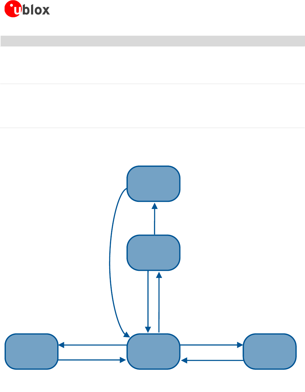
Transition between the different modes is described in Figure 3.
Switch ON:
•Apply VCC
If power saving is enabled
and there is no activity for a
defined time interval
Any wake up event described
in the module operating
modes summary table above
AT+CPWROFF
(no HW pin)
Incoming/outgoing call or
other dedicated device
network communication
Call terminated,
communication dropped
Remove VCC
Switch ON:
•PWR_ON
•RESET_N
•RTC Alarm
Not
powered
Power off
ActiveConnected Idle
Figure 3: Operating modes transition
LISA-U1/LISA-H1 series - System Integration Manual
3G.G2-HW-10002-2 Advance Information System description
Page 16 of 116
1.5 Power management
1.5.1 Power supply circuit overview
LISA-U1/LISA-H1 series modules feature a power management concept optimized for the most efficient use of
supplied power. This is achieved by hardware design utilizing a power efficient circuit topology (Figure 4), and by
power management software controlling the module’s power saving mode.
Baseband Processor
2G Power Amplifier
Switching
Step-Down
LISA-U1/LISA-H1 series
5 x 10 µF
61
VCC
62
VCC
63
VCC
50
VSIM
2
V_BCKP
4
V_INT
2 x 3G Power Amplifier(s)
Linear
LDO
Linear
LDO
Switching
Step-Down
Linear
LDO
Linear
LDO
Linear
LDO
I/O
EBU
CORE
Analog
SIM
RTC
NOR
Flash
DDR
SRAM
RF Transceiver
Memory
Power Management Unit
Figure 4: Power management simplified block diagram
Pins with supply function are reported in Table 3, Table 7 and Table 9.
LISA-U1/LISA-H1 series modules must be supplied via the VCC pins. There is only one main power supply input,
available on the three VCC pins that must be all connected to the external power supply
The VCC pins are directly connected to the RF power amplifiers and to the integrated Power Management Unit
(PMU) within the module: all supply voltages needed by the module are generated from the VCC supply by
integrated voltage regulators.

LISA-U1/LISA-H1 series - System Integration Manual
3G.G2-HW-10002-2 Advance Information System description
Page 17 of 116
V_BCKP is the Real Time Clock (RTC) supply. When the VCC voltage is within the valid operating range, the
internal PMU supplies the Real Time Clock and the same supply voltage will be available to the V_BCKP pin. If
the VCC voltage is under the minimum operating limit (for example, during not powered mode), the Real Time
Clock can be externally supplied via the V_BCKP pin (see section 1.5.4).
When a 1.8 V or a 3 V SIM card type is connected, LISA-U1/LISA-H1 series modules automatically supply the SIM
card via the VSIM pin. Activation and deactivation of the SIM interface with automatic voltage switch from 1.8
to 3 V is implemented, in accordance to the ISO-IEC 7816-3 specifications.
The same voltage domain used internally to supply the digital interfaces is also available on the V_INT pin, to
allow more economical and efficient integration of the LISA-U1/LISA-H1 series modules in the final application.
The integrated Power Management Unit also provides the control state machine for system start up and system
reset control.
1.5.2 Module supply (VCC)
The LISA-U1/LISA-H1 series modules must be supplied through the VCC pins by a DC power supply. Voltages
must be stable: during operation, the current drawn from VCC can vary by some orders of magnitude, especially
due to surging consumption profile of the GSM system (described in the section 1.5.3). It is important that the
system power supply circuit is able to support peak power (refer to LISA-U1/LISA-H1 series Data Sheet [1] for
specification).
Name
Description
Remarks
VCC
Module power supply input
VCC pins are internally connected, but all the available pads
must be connected to the external supply in order to
minimize the power loss due to series resistance.
Clean and stable supply is required: low ripple and low
voltage drop must be guaranteed.
Voltage provided must always be above the minimum limit of
the operating range.
Consider that during a GSM call there are large current spikes
in connected mode.
GND
Ground
GND pins are internally connected but a good (low
impedance) external ground can improve RF performance: all
available pads must be connected to ground.
Table 3: Module supply pins
VCC pins ESD rating is 1 kV (contact discharge). A higher protection level can be required if the line is
externally accessible on the application board. A higher protection level can be achieved by mounting an
ESD protection (e.g. EPCOS CA05P4S14THSG varistor array) on the line connected to this pin.
The voltage provided to the VCC pins must be within the normal operating range limits as specified in the
LISA-U1/LISA-H1 series Data Sheet [1]. Complete functionality of the module is only guaranteed within the
specified minimum and maximum VCC voltage operating range.
Ensure that the input voltage at the VCC pins never drops below the minimum limit of the operating
range when the module is switched on. This is the case even during a GSM transmit burst, where the
current consumption can rise up to minimum peaks of 2.5 A in case of a mismatched antenna load.
Operation above the operating range maximum limit is not recommended and extended
exposure beyond it may affect device reliability.
LISA-U1/LISA-H1 series - System Integration Manual
3G.G2-HW-10002-2 Advance Information System description
Page 18 of 116
Stress beyond the VCC absolute maximum ratings can cause permanent damage to the
module: if necessary, voltage spikes beyond VCC absolute maximum ratings must be restricted
to values within the specified limits by using appropriate protection.
When designing the power supply for the application, pay specific attention to power losses and
transients. The DC power supply must be able to provide a voltage profile to the VCC pins with the
following characteristics:
Voltage drop during transmit slots must be lower than 400 mV
No undershoot or overshoot at the start and at the end of transmit slots
Voltage ripple during transmit slots must be minimized
Time
undershoot
overshoot
ripple
ripple
drop
Voltage
3.8 V
(typ)
RX
slot
unused
slot
unused
slot
TX
slot
unused
slot
unused
slot
MON
slot
unused
slot
RX
slot
unused
slot
unused
slot
TX
slot
unused
slot
unused
slot
MON
slot
unused
slot
GSM frame
4.615 ms
(1 frame = 8 slots)
GSM frame
4.615 ms
(1 frame = 8 slots)
Figure 5: Description of the VCC voltage profile versus time during a GSM call
Any degradation in power supply performance (due to losses, noise or transients) will directly affect the
RF performance of the module since the single external DC power source indirectly supplies all the
digital and analog interfaces, and also directly supplies the RF power amplifier (PA).
The voltage at the VCC pins must ramp from 2.5 V to 3.2 V within 1 ms. This VCC slope allows a proper
switch on of the module, that is switched on when the voltage rises to the VCC operating range starting
from a voltage value lower than 2.25 V.
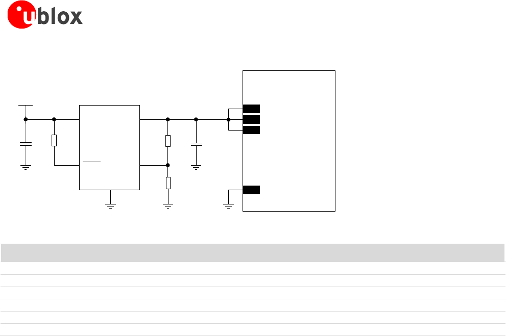
1.5.2.1 VCC application circuits
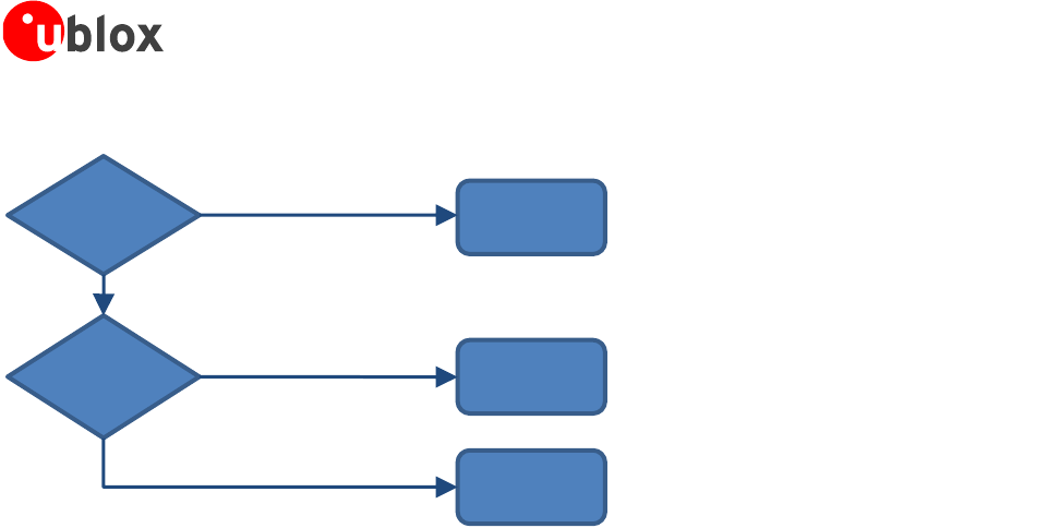
LISA-U1/LISA-H1 series modules must be supplied through the VCC pins by one (and only one) proper DC power
supply that must be one of the following:
Switching regulator
Low Drop-Out (LDO) linear regulator
Rechargeable Li-Ion battery
Primary (disposable) battery
LISA-U1/LISA-H1 series - System Integration Manual
3G.G2-HW-10002-2 Advance Information System description
Page 19 of 116
Main Supply
Available?
Battery
Li-Ion 3.7 V
Linear LDO
Regulator
Main Supply
Voltage
>5 V?
Switching
Step-Down
Regulator
No, portable device
No, less than 5 V
Yes, greater than 5 V
Yes, always available
Figure 6: VCC supply concept selection
The switching step-down regulator is the typical choice when the available primary supply source has a nominal
voltage much higher (e.g. greater than 5 V) than the LISA-U1/LISA-H1 series modules operating supply voltage.
The use of switching step-down provides the best power efficiency for the overall application and minimizes
current drawn from the main supply source.
The use of an LDO linear regulator becomes convenient for a primary supply with a relatively low voltage (e.g.
less than 5 V). In this case the typical 90% efficiency of the switching regulator will diminish the benefit of
voltage step-down and no true advantage will be gained in input current savings. On the opposite side, linear
regulators are not recommended for high voltage step-down as they will dissipate a considerable amount of
energy in thermal power.
If LISA-U1/LISA-H1 series modules are deployed in a mobile unit where no permanent primary supply source is
available, then a battery will be required to provide VCC. A standard 3-cell Lithium-Ion battery pack directly
connected to VCC is the usual choice for battery-powered devices. During charging, batteries with Ni-MH
chemistry typically reach a maximum voltage that is above the maximum rating for VCC, and should therefore be
avoided.
The use of primary (not rechargeable) battery is uncommon, since the most cells available are seldom capable of
delivering the burst peak current for a GSM call due to high internal resistance.
Keep in mind that the use of batteries requires the implementation of a suitable charger circuit (not included in
LISA-U1/LISA-H1 series modules). The charger circuit should be designed in order to prevent over-voltage on
VCC beyond the upper limit of the absolute maximum rating.
The following sections highlight some design aspects for each of the supplies listed above.
Switching regulator
The characteristics of the switching regulator connected to VCC pins should meet the following requirements:
Power capability: the switching regulator with its output circuit must be capable of providing a voltage
value to the VCC pins within the specified operating range and must be capable of delivering 2.5 A current
pulses with 1/8 duty cycle to the VCC pins
Low output ripple: the switching regulator together with its output circuit must be capable of providing a
clean (low noise) VCC voltage profile
High switching frequency: for best performance and for smaller applications select a switching frequency
≥ 600 kHz (since L-C output filter is typically smaller for high switching frequency). The use of a switching
regulator with a variable switching frequency or with a switching frequency lower than 600 kHz must be
carefully evaluated since this can produce noise in the VCC voltage profile and therefore negatively impact
GSM modulation spectrum performance. An additional L-C low-pass filter between the switching regulator
LISA-U1/LISA-H1 series - System Integration Manual
3G.G2-HW-10002-2 Advance Information System description
Page 20 of 116
output to VCC supply pins can mitigate the ripple on VCC, but adds extra voltage drop due to resistive
losses on series inductors
PWM mode operation: select preferably regulators with Pulse Width Modulation (PWM) mode. While in
active mode Pulse Frequency Modulation (PFM) mode and PFM/PWM mode transitions must be avoided to
reduce the noise on the VCC voltage profile. Switching regulators able to switch between low ripple PWM
mode and high efficiency burst or PFM mode can be used, provided the mode transition occurs when the
GSM module changes status from idle mode (current consumption approximately 1 mA) to active mode
(current consumption approximately 100 mA): it is permissible to use a regulator that switches from the
PWM mode to the burst or PFM mode at an appropriate current threshold (e.g. 60 mA)
Output voltage slope: the use of the soft start function provided by some voltage regulator must be
carefully evaluated, since the voltage at the VCC pins must ramp from 2.5 V to 3.2 V within 1 ms to allow a
proper switch-on of the module
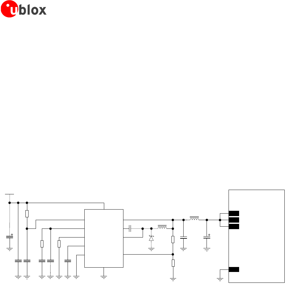
Figure 7 and the components listed in Table 4 show an example of a high reliability power supply circuit, where
the module VCC is supplied by a step-down switching regulator capable of delivering 2.5 A current pulses with
low output ripple and with fixed switching frequency in PWM mode operation greater than 1 MHz. The use of a
switching regulator is suggested when the difference from the available supply rail to the VCC value is high:
switching regulators provide good efficiency transforming a 12 V supply to the typical 3.8 V value of the VCC
supply.
LISA-U1/LISA-H1
series
12V
C6
R3
C5
R2
C3C2
C1
R1
VIN
RUN
VC
RT
PG
SYNC
BD
BOOST
SW
FB
GND
6
7
10
9
5
C7
1
2
3
8
11
4
C8 C9
L2
D1 R4
R5
L1
C4
U1
62 VCC
63 VCC
61 VCC
GND
Figure 7: Suggested schematic design for the VCC voltage supply application circuit using a step-down regulator
LISA-U1/LISA-H1 series - System Integration Manual
3G.G2-HW-10002-2 Advance Information System description
Page 21 of 116
Reference
Description
Part Number - Manufacturer
C1
47 µF Capacitor Aluminum 0810 50 V
MAL215371479E3 - Vishay
C2
10 µF Capacitor Ceramic X7R 5750 15% 50 V
C5750X7R1H106MB - TDK
C3
10 nF Capacitor Ceramic X7R 0402 10% 16 V
GRM155R71C103KA01 - Murata
C4
680 pF Capacitor Ceramic X7R 0402 10% 16 V
GRM155R71H681KA01 - Murata
C5
22 pF Capacitor Ceramic COG 0402 5% 25 V
GRM1555C1H220JZ01 - Murata
C6
10 nF Capacitor Ceramic X7R 0402 10% 16 V
GRM155R71C103KA01 - Murata
C7
470 nF Capacitor Ceramic X7R 0603 10% 25 V
GRM188R71E474KA12 - Murata
C8
22 µF Capacitor Ceramic X5R 1210 10% 25 V
GRM32ER61E226KE15 - Murata
C37
330 µF Capacitor Tantalum D_SIZE 6.3 V 45 mΩ
T520D337M006ATE045 - KEMET
D1
Schottky Diode 40 V 3 A
MBRA340T3G - ON Semiconductor
L1
10 µH Inductor 744066100 30% 3.6 A
744066100 - Wurth Electronics
L2
1 µH Inductor 7445601 20% 8.6 A
7445601 - Wurth Electronics
R1
470 kΩ Resistor 0402 5% 0.1 W
2322-705-87474-L - Yageo
R2
15 kΩ Resistor 0402 5% 0.1 W
2322-705-87153-L - Yageo
R3
22 kΩ Resistor 0402 5% 0.1 W
2322-705-87223-L - Yageo
R4
390 kΩ Resistor 0402 1% 0.063 W
RC0402FR-07390KL - Yageo
R5
100 kΩ Resistor 0402 5% 0.1 W
2322-705-70104-L - Yageo
U1
Step Down Regulator MSOP10 3.5 A 2.4 MHz
LT3972IMSE#PBF - Linear Technology
Table 4: Suggested components for the VCC voltage supply application circuit using a step-down regulator
Low Drop-Out (LDO) linear regulator
The characteristics of the LDO linear regulator connected to the VCC pins should meet the following
requirements:
Power capabilities: the LDO linear regulator with its output circuit must be capable of providing a proper
voltage value to the VCC pins and of delivering 2.5 A current pulses with 1/8 duty cycle
Power dissipation: the power handling capability of the LDO linear regulator must be checked to limit its
junction temperature to the maximum rated operating range (i.e. check the voltage drop from the max input
voltage to the min output voltage to evaluate the power dissipation of the regulator)
Output voltage slope: the use of the soft start function provided by some voltage regulators must be
carefully evaluated, since the voltage at the VCC pins must ramp from 2.5 V to 3.2 V within 1 ms to allow a
proper switch-on of the module
Figure 8 and the components listed in Table 5 show an example of a power supply circuit, where the VCC
module supply is provided by an LDO linear regulator capable of delivering 2.5 A current pulses, with proper
power handling capability. The use of a linear regulator is suggested when the difference from the available
supply rail and the VCC value is low: linear regulators provide high efficiency when transforming a 5 V supply to
the 3.8 V typical value of the VCC supply.
LISA-U1/LISA-H1 series - System Integration Manual
3G.G2-HW-10002-2 Advance Information System description
Page 22 of 116
5V
C1 R1
IN OUT
ADJ
GND
1
24
5
3
C2R2
R3
U1
SHDN
LISA-U1/LISA-H1
series
62 VCC
63 VCC
61 VCC
GND
Figure 8: Suggested schematic design for the VCC voltage supply application circuit using an LDO linear regulator
Reference
Description
Part Number - Manufacturer
C1
10 µF Capacitor Ceramic X5R 0603 20% 6.3 V
GRM188R60J106ME47 - Murata
C2
10 µF Capacitor Ceramic X5R 0603 20% 6.3 V
GRM188R60J106ME47 - Murata
R1
47 kΩ Resistor 0402 5% 0.1 W
RC0402JR-0747KL - Yageo Phycomp
R2
4.7 kΩ Resistor 0402 5% 0.1 W
RC0402JR-074K7L - Yageo Phycomp
R3
2.2 kΩ Resistor 0402 5% 0.1 W
RC0402JR-072K2L - Yageo Phycomp
U1
LDO Linear Regulator ADJ 3.0 A
LT1764AEQ#PBF - Linear Technology
Table 5: Suggested components for VCC voltage supply application circuit using an LDO linear regulator
Rechargeable Li-Ion battery
Rechargeable Li-Ion batteries connected to the VCC pins should meet the following requirements:
Maximum pulse and DC discharge current: the rechargeable Li-Ion battery with its output circuit must be
capable of delivering 2.5 A current pulses with 1/8 duty-cycle to the VCC pins and must be capable of
delivering a DC current greater than the module maximum average current consumption to VCC pins. The
maximum pulse discharge current and the maximum DC discharge current are not always reported in
battery data sheets, but the maximum DC discharge current is typically almost equal to the battery capacity
in Amp-hours divided by 1 hour
DC series resistance: the rechargeable Li-Ion battery with its output circuit must be capable of avoiding a
VCC voltage drop greater than 400 mV during transmit bursts
Primary (disposable) battery
The characteristics of a primary (non-rechargeable) battery connected to VCC pins should meet the following
requirements:
Maximum pulse and DC discharge current: the non-rechargeable battery with its output circuit must be
capable of delivering 2.5 A current pulses with 1/8 duty-cycle to the VCC pins and must be capable of
delivering a DC current greater than the module maximum average current consumption at the VCC pins.
The maximum pulse and the maximum DC discharge current is not always reported in battery data sheets,
but the maximum DC discharge current is typically almost equal to the battery capacity in Amp-hours
divided by 1 hour
DC series resistance: the non-rechargeable battery with its output circuit must be capable of avoiding a
VCC voltage drop greater than 400 mV during transmit bursts
LISA-U1/LISA-H1 series - System Integration Manual
3G.G2-HW-10002-2 Advance Information System description
Page 23 of 116
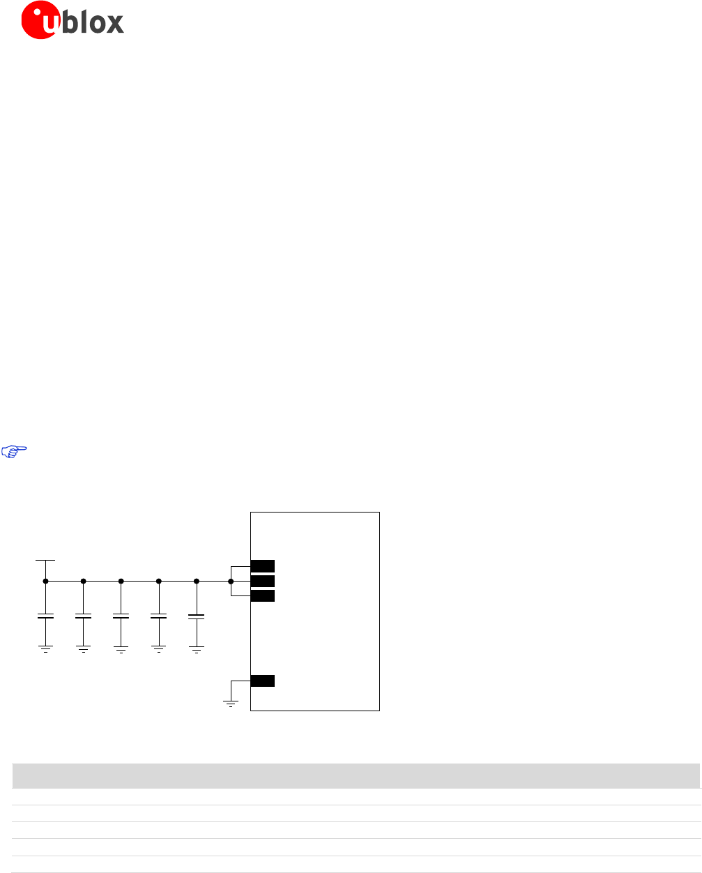
Additional hints for the VCC supply application circuits
To reduce voltage drops, use a low impedance power source. The resistance of the power supply lines
(connected to the VCC and GND pins of the module) on the application board and battery pack should also be
considered and minimized: cabling and routing must be as short as possible in order to minimize power losses.
Three pins are allocated for VCC supply. Another twenty pins are designated for GND connection. Even if all the
VCC pins and all the GND pins are internally connected within the module, it is recommended to properly
connect all of them to supply the module in order to minimize series resistance losses.
To avoid undershoot and overshoot on voltage drops at the start and end of a transmit burst during a GSM call
(when current consumption on the VCC supply can rise up to 2.5 A in the worst case), place a 330 µF low ESR
capacitor (e.g. KEMET T520D337M006ATE045) near the VCC pins.
The use of very large capacitors (i.e. greater then 1000 µF) on the VCC line and the use of the soft start function
provided by some voltage regulators must be carefully evaluated, since the voltage at the VCC pins must ramp
from 2.5 V to 3.2 V within 1 ms to allow a proper switch on of the module.To reduce voltage ripple and noise,
place the following near the VCC pins:
100 nF capacitor (e.g Murata GRM155R61A104K) to filter digital logic noise from clocks and data sources
10 nF capacitor (e.g. Murata GRM155R71C103K) to filter digital logic noise from clocks and data sources
10 pF capacitor (e.g. Murata GRM1555C1E100J) to filter EMI in the 1800 / 1900 / 2100 MHz bands
39 pF capacitor (e.g. Murata GRM1555C1E390J) to filter EMI in the 850 / 900 MHz bands
Figure 9 shows the complete configuration but the mounting of each single component depends on the
application design.
3V8
C1 C4
GND
C3C2 C5
LISA-U1/LISA-H1
series
62 VCC
63 VCC
61 VCC
+
Figure 9: Suggested schematic design to reduce voltage ripple and noise and to avoid undershoot/ overshoot on voltage drops
Reference
Description
Part Number - Manufacturer
C1
330 µF Capacitor Tantalum D_SIZE 6.3 V 45 mΩ
T520D337M006ATE045 - KEMET
C2
100 nF Capacitor Ceramic X7R 0402 10% 16 V
GRM155R61A104KA01 - Murata
C3
10 nF Capacitor Ceramic X7R 0402 10% 16 V
GRM155R71C103KA01 - Murata
C4
39 pF Capacitor Ceramic C0G 0402 5% 25 V
GRM1555C1E390JA01 - Murata
C5
10 pF Capacitor Ceramic C0G 0402 5% 25 V
GRM1555C1E100JA01 - Murata
Table 6: Suggested components to reduce voltage ripple and noise and to avoid undershoot/ overshoot on voltage drops
LISA-U1/LISA-H1 series - System Integration Manual
3G.G2-HW-10002-2 Advance Information System description
Page 24 of 116
1.5.3 Current consumption profiles
During operation, the current drawn by the LISA-U1/LISA-H1 series modules through the VCC pins can vary by
several orders of magnitude. This ranges from the high peak of current consumption during GSM transmitting
bursts at maximum power level in 2G connected mode, to continuous high current drawn in UMTS connected
mode, to the low current consumption during power saving in idle mode.
1.5.3.1 2G connected mode
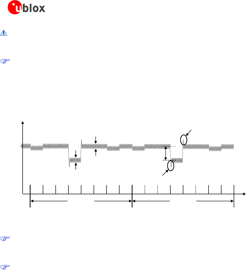
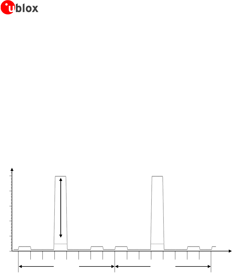
When a GSM call is established, the VCC consumption is determined by the current consumption profile typical
of the GSM transmitting and receiving bursts.
The current consumption peak during a transmission slot is strictly dependent on the transmitted power, which
is regulated by the network. If the module is transmitting in GSM talk mode in the GSM 850 or in the E-GSM
900 band and at the maximum RF power control level (approximately 2 W or 33 dBm in the allocated transmit
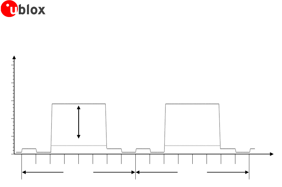
slot/burst) the current consumption can reach up to 2500 mA (with a highly unmatched antenna) for 576.9 µs
(width of the transmit slot/burst) with a periodicity of 4.615 ms (width of 1 frame = 8 slots/burst), so with a 1/8
duty cycle according to GSM TDMA (Time Division Multiple Access).
During a GSM call, current consumption is in the order of 100-200 mA in receiving or in monitor bursts and is
about 30-50 mA in the inactive unused bursts (low current period). The more relevant contribution to determine
the average current consumption is set by the transmitted power in the transmit slot.
An example of current consumption profile of the data module in GSM talk mode is shown in Figure 10.
Time [ms]
RX
slot
unused
slot
unused
slot
TX
slot
unused
slot
unused
slot
MON
slot
unused
slot
RX
slot
unused
slot
unused
slot
TX
slot
unused
slot
unused
slot
MON
slot
unused
slot
GSM frame
4.615 ms
(1 frame = 8 slots)
Current [A]
200 mA ~170 mA
2500 mA
Peak current
depends on
TX power
GSM frame
4.615 ms
(1 frame = 8 slots)
1.5
1.0
0.5
0.0
2.5
2.0
~170 mA ~40 mA
Figure 10: VCC current consumption profile versus time during a GSM call (1 TX slot, 1 RX slot), with VCC=3.8 V
When a GPRS connection is established there is a different VCC current consumption profile also determined by
the transmitting and receiving bursts. In contrast to a GSM call, during a GPRS connection more than one slot
can be used to transmit and/or more than one slot can be used to receive. The transmitted power depends on
network conditions, which set the peak current consumption, but following the GPRS specifications the
maximum transmitted RF power is reduced if more than one slot is used to transmit, so the maximum peak of
current consumption is not as high as can be in case of a GSM call.
If the module transmits in GPRS class 12 connected mode in the GSM 850 or in the E-GSM 900 band at the
maximum power control level (27 dBm typical transmitted power in the transmit slot/burst), the current
consumption can reach up to 1400 mA (with unmatched antenna). This happens for 2.307 ms (width of the 4
transmit slots/bursts) with a periodicity of 4.615 ms (width of 1 frame = 8 slots/bursts), so with a 1/2 duty cycle,
according to GSM TDMA.
LISA-U1/LISA-H1 series - System Integration Manual
3G.G2-HW-10002-2 Advance Information System description
Page 25 of 116
Figure 11 reports the current consumption profiles in GPRS mode with 4 slots used to transmit.
Time [ms]
RX
slot
unused
slot
TX
slot
TX
slot
TX
slot
TX
slot
MON
slot
unused
slot
RX
slot
unused
slot
TX
slot
TX
slot
TX
slot
TX
slot
MON
slot
unused
slot
GSM frame
4.615 ms
(1 frame = 8 slots)
Current [A]
200mA ~170mA
Peak current
depends on
TX power
~170mA
GSM frame
4.615 ms
(1 frame = 8 slots)
1.5
1.0
0.5
0.0
2.5
2.0
~40mA
1400 mA
Figure 11: VCC current consumption profile versus time during a GPRS/EDGE connection (4TX slots, 1 RX slot), with VCC=3.8 V
In case of EDGE connections the VCC current consumption profile is very similar to the GPRS current profile, so
the image shown in Figure 11 is valid for EDGE as well.
1.5.3.2 3G connected mode
During a 3G connection, the module can transmit and receive continuously due to the Frequency Division Duplex
(FDD) mode of operation with the Wideband Code Division Multiple Access (WCDMA). The current consumption
depends again on output RF power, which is always regulated by network commands. These power control
commands are logically divided into a slot of 666 µs, thus the rate of power change can reach a maximum rate
of 1.5 kHz. There are no high current peaks as in the 2G connection, since transmission and reception are
continuously enabled due to FDD WCDMA implemented in the 3G that differs from the TDMA implemented in
the 2G case. In the worst scenario, corresponding to a continuous transmission and reception at maximum
output power (approximately 250 mW or 24 dBm), the current drawn by the module at the VCC pins is in the
order of continuous 600-700 mA. Even at lowest output RF power (approximately 0.01 µW or -50 dBm), the
current still remains in the order of 200 mA due to module baseband processing and transceiver activity.
An example of current consumption profile of the data module in UMTS continuous transmission mode is shown
in Figure 12.
LISA-U1/LISA-H1 series - System Integration Manual
3G.G2-HW-10002-2 Advance Information System description
Page 26 of 116
Time
[ms]
3G frame
10 ms
(1 frame = 15 slots)
Current [mA]
170 mA
Depends
on TX
power
1 slot
666 µs
670 mA
300
200
100
0
500
400
600
700
Figure 12: VCC current consumption profile versus time during a UMTS connection, with VCC=3.8 V
When a packet data connection is established, the actual current profile depends on the amount of transmitted
packets; there might be some periods of inactivity between allocated slots where current consumption drops
about 100 mA. Alternatively, at higher data rates the transmitted power is likely to increase due to the higher
quality signal required by the network to cope with enhanced data speed.
1.5.3.3 2G and 3G cyclic idle/active mode (power saving enabled)
The power saving configuration is by default disabled, but it can be enabled using the appropriate AT command
(refer to u-blox AT Commands Manual [2], AT+UPSV command). When the power saving is enabled, the module
automatically enters idle-mode whenever possible.
When power saving is enabled, the module is registered or attached to a network and a voice or data call is not
enabled, the module automatically enters idle-mode whenever possible, but it must periodically monitor the
paging channel of the current base station (paging block reception), in accordance to GSM system requirements.
When the module monitors the paging channel, it wakes up to active mode, to enable the reception of paging
block. In between, the module switches to idle-mode. This is known as GSM discontinuous reception (DRX).
The module processor core is activated during the paging block reception, and automatically switches its
reference clock frequency from 32 kHz to the 26 MHz used in active-mode.
The time period between two paging block receptions is defined by the network (2G or 3G). This is the paging
period parameter, fixed by the base station through broadcast channel sent to all users on the same serving cell.
In case of 2G network, the time interval between two paging block receptions can be from 470.76 ms (width of
2 GSM multiframes = 2 x 51 GSM frames = 2 x 51 x 4.615 ms) up to 2118.42 ms (width of 9 GSM multiframes
= 9 x 51 frames = 9 x 51 x 4.615 ms).
In case of 3G network, the principle is similar but time interval changes from 640 ms (width of 26 x 3G frames =
64 x 10 ms = 640 ms) up to 5120 ms (width of 29 x 3G frames = 512 x 10 ms = 5120 ms).
An example of a module current consumption profile is shown in Figure 13: the module is registered with the
network (2G or 3G), automatically enters idle mode and periodically wakes up to active mode to monitor the
paging channel for paging block reception.
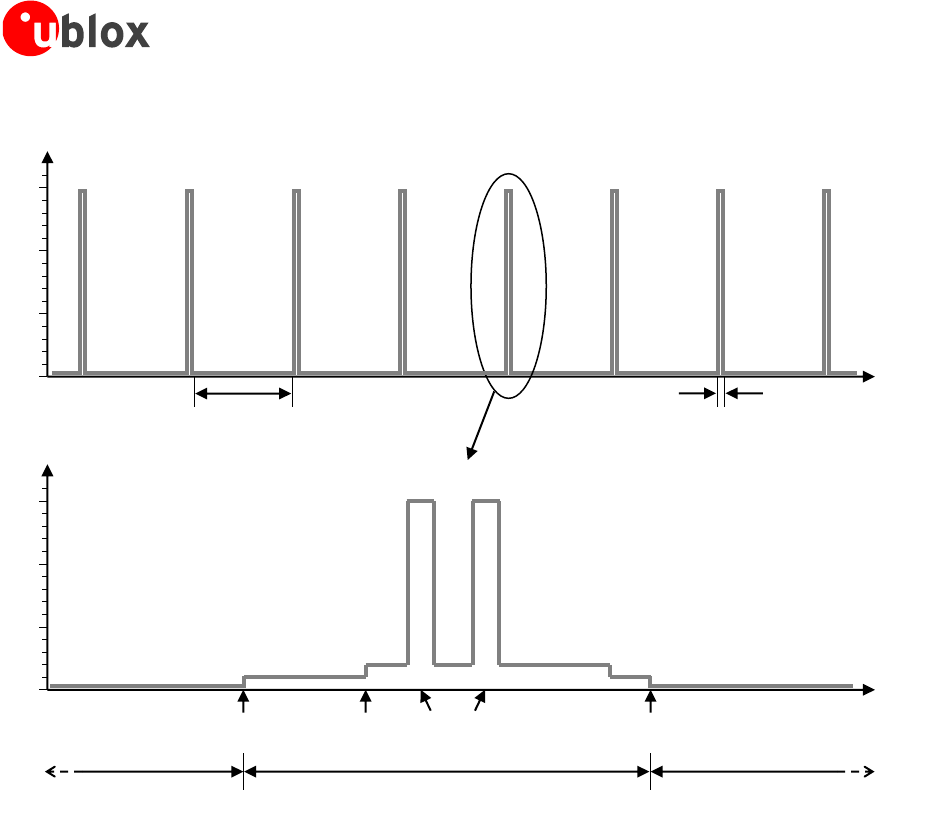
LISA-U1/LISA-H1 series - System Integration Manual
3G.G2-HW-10002-2 Advance Information System description
Page 27 of 116
~30 ms
IDLE MODE ACTIVE MODE IDLE MODE
500-700 µA 8-10 mA 20-22 mA
~150 mA
Active Mode
Enabled
Idle Mode
Enabled
PLL
Enabled
RX+DSP
Enabled
500-700 µA
~150 mA
2G case: 0.44-2.09 s
3G case: 0.61-5.09 s
IDLE MODE
2G or 3G case: ~30 ms
ACTIVE MODE
Time [s]
Current [mA]
150
100
50
0
Time [ms]
Current [mA]
150
100
50
0
Figure 13: Description of VCC current consumption profile versus time when the module is registered with 2G or 3G networks:
the module is in idle mode and periodically wakes up to active mode to monitor the paging channel for paging block reception
1.5.3.4 2G and 3G fixed active mode (power saving disabled)
Power saving configuration is by default disabled, or it can be disabled using the appropriate AT command (refer
to u-blox AT Commands Manual [2], AT+UPSV command). When power saving is disabled, the module doesn’t
automatically enter idle-mode whenever possible: the module remains in active mode.
The module processor core is activated during active-mode, and the 26 MHz reference clock frequency is used.
An example of the current consumption profile of the data module when power saving is disabled is shown in
Figure 14: the module is registered with the network, active-mode is maintained, and the receiver and the DSP
are periodically activated to monitor the paging channel for paging block reception.
LISA-U1/LISA-H1 series - System Integration Manual
3G.G2-HW-10002-2 Advance Information System description
Page 28 of 116
ACTIVE MODE
20-22 mA 20-22 mA
~150 mA
RX+DSP
Enabled
20-22 mA
~150 mA
2G case: 0.47-2.12 s
3G case: 0.64-5.12 s
Paging period
Time [s]
Current [mA]
150
100
50
0
Time [ms]
Current [mA]
150
100
50
0
Figure 14: Description of the VCC current consumption profile versus time when power saving is disabled: active-mode is
always held, and the receiver and the DSP are periodically activated to monitor the paging channel for paging block reception
1.5.4 RTC Supply (V_BCKP)
The V_BCKP pin connects the supply for the Real Time Clock (RTC) and Power On / Reset internal logic. This
supply domain is internally generated by a linear regulator integrated in the Power Management Unit. The
output of this linear regulator is always enabled when the main voltage supply provided to the module through
VCC is within the valid operating range, with the module switched-off or powered-on.
Name
Description
Remarks
V_BCKP
Real Time Clock supply
V_BCKP = 2.3 V (typical) generated by the module to supply
Real Time Clock when VCC supply voltage is within valid
operating range.
Table 7: Real Time Clock supply pin
The V_BCKP pin ESD rating is 1 kV (contact discharge). A higher protection level could be required if the
line is externally accessible on the application board. A higher protection level can be achieved by
mounting an ESD protection (e.g. EPCOS CA05P4S14THSG varistor array) on the line connected to this
pin.
The RTC provides the time reference (date and time) of the module, also in power off mode, when the V_BCKP
voltage is within its valid range (specified in u-blox LISA-U1/LISA-H1 series Data Sheet [1]). The RTC timing is
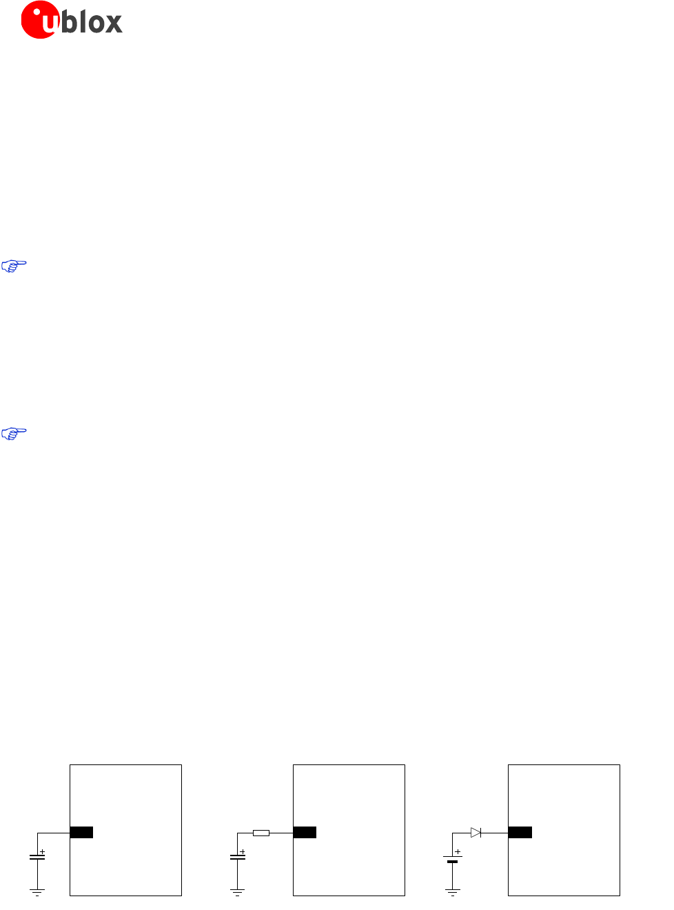
LISA-U1/LISA-H1 series - System Integration Manual
3G.G2-HW-10002-2 Advance Information System description
Page 29 of 116
normally used to set the wake-up interval during idle-mode periods between network paging, but is able to
provide programmable alarm functions by means of the internal 32.768 kHz clock.
The RTC can be supplied from an external back-up battery through the V_BCKP, when the main voltage supply
is not provided to the module through VCC. This lets the time reference (date and time) run even when the main
supply is not provided to the module. Consider that the module cannot switch on if a valid voltage is not present
on VCC even when the RTC is supplied through V_BCKP (meaning that VCC is mandatory to switch-on the
module).
The RTC has very low power consumption, but is highly temperature dependent. For example at 25°C and a
V_BCKP voltage of 2.3 V the power consumption is approximately 2 µA, whereas at 70°C and an equal voltage
the power consumption increases to 5-10 µA.
The internal regulator for V_BCKP is optimized for low leakage current and very light loads. It is not
recommended to use V_BCKP to supply external loads.
If V_BCKP is left unconnected and the module main voltage supply is removed from VCC, the RTC is supplied
from the 100 nF capacitor mounted inside the module. However, this capacitor is not able to provide a long
buffering time: within few milliseconds the voltage on V_BCKP will go below the valid range (1 V min). At this
time the internal RTC will stop counting and the date and time setting will be lost. This has no impact on
wireless connectivity, as all the functionalities of the module do not rely on the date and time setting.
Leave V_BCKP unconnected if the RTC is not required when the VCC supply is removed. The date and
time will not be updated when VCC is disconnected. If VCC is always supplied, then the internal
regulator is supplied from the main supply and there is no need for an external component on V_BCKP.
If RTC is required to run for a time interval of T [s] at 25°C when VCC supply is removed, place a capacitor with a
nominal capacitance of C [µF] at the V_BCKP pin. Choose the capacitor using the following formula:
C [µF] = (Current_Consumption [µA] x T [s]) / Voltage_Drop [V] = 1.538 x T [s]
The RTC current consumption is approximately 2 µA at 25°C, and the voltage drop is equal to 1.3 V (from the
V_BCKP typical value of 2.3 V to the valid range minimum limit of 1.0 V).
For example, a 100 µF capacitor (such as the Murata GRM43SR60J107M) can be placed at V_BCKP to provide a
long buffering time. This capacitor will hold V_BCKP voltage within its valid range for around 50 s at 25°C, after
the VCC supply is removed. If a very long buffering time is required, a 70 mF super-capacitor (e.g. Seiko
Instruments XH414H-IV01E) can be placed at V_BCKP, with a 4.7 k series resistor to hold the V_BCKP voltage
within its valid range for approximately 10 hours at 25°C, after the VCC supply is removed. The purpose of the
series resistor is to limit the capacitor charging current due to the large capacitor specifications, and also to let a
fast rise time of the voltage value at the V_BCKP pin after VCC supply has been provided. These capacitors will
allow the time reference to run during battery disconnection.
LISA-U1/LISA-H1
series
C1
(a)
2V_BCKP
R2
LISA-U1/LISA-H1
series
C2
(superCap)
(b)
2V_BCKP
D3
LISA-U1/LISA-H1
series
2.3 V
(c)
2V_BCKP
Figure 15: Real time clock supply (V_BCKP) application circuits : (a) using a 100 µF capacitor to let the RTC run for ~50 s at 25°C;
(b) using a 70 mF capacitor to let the RTC run for ~10 hours at 25°C when the VCC supply is removed; (c) using non-rechargeable
battery

LISA-U1/LISA-H1 series - System Integration Manual
3G.G2-HW-10002-2 Advance Information System description
Page 30 of 116
Reference
Description
Part Number - Manufacturer
C1
100 µF Tantalum Capacitor
GRM43SR60J107M - Murata
R2
4.7 kΩ Resistor 0402 5% 0.1 W
RC0402JR-074K7L - Yageo Phycomp
C2
70 mF Capacitor
XH414H-IV01E - Seiko Instruments
Table 8: Example of components for V_BCKP buffering
If longer buffering time is required to allow the time reference to run during a disconnection of the VCC supply,
then an external battery can be connected to V_BCKP pin. The battery should be able to provide a 2.3 V
nominal voltage and must never exceed the maximum operating voltage for V_BCKP. The connection of the
battery to V_BCKP should be done with a suitable series resistor for a rechargeable battery, or with an
appropriate series diode for a non-rechargeable battery. The purpose of the series resistor is to limit the battery
charging current due to the battery specifications, and also to allow a fast rise time of the voltage value at the
V_BCKP pin after the VCC supply has been provided. The purpose of the series diode is to avoid a current flow
from the module V_BCKP pin to the non-rechargeable battery.
1.5.5 Interface supply (V_INT)
The same voltage domain used internally to supply the digital interfaces is also available on the V_INT pin. The
internal regulator that generates the V_INT supply is a switching step down converter that is directly supplied
from VCC. The voltage regulator output is set to 1.8 V (typical) when the module is switched on and is disabled
when the module is switched off or when the RESET_N pin is forced the low level. The switching regulator
operates in Pulse Width Modulation (PWM) for high output current mode but automatically switches to Pulse
Frequency Modulation (PFM) at low output loads for greater efficiency, e.g. when the module is in idle mode
between paging periods.
Name
Description
Remarks
V_INT
Digital Interfaces supply output
V_INT = 1.8V (typical) generated by the module when it is
switched-on and the RESET_N (external reset input pin) is
not forced to the low level.
V_INT is the internal supply for digital interfaces.
The user may draw limited current from this supply rail.
Table 9: Interface supply pin
The V_INT pin ESD rating is 1 kV (contact discharge). A higher protection level could be required if the
line is externally accessible on the application board. A higher protection level can be achieved by
mounting an ESD protection (e.g. EPCOS CA05P4S14THSG varistor array) on the line connected to this
pin.
Since it supplies internal digital circuits (see Figure 4), V_INT is not suited to directly supply any sensitive analog
circuit: the voltage ripple can range from 15 mVpp during active mode (PWM), to 70 mVpp in idle mode (PFM).
V_INT can be used to supply external digital circuits operating at the same voltage level as the digital
interface pins, i.e. 1.8 V (typical). It is not recommended to supply analog circuitry without adequate
filtering for digital noise.
Don’t apply loads which might exceed the limit for maximum available current from V_INT supply, as
this can cause malfunctions in internal circuitry supplies to the same domain. The detailed electrical
characteristics are described in the LISA-U1/LISA-H1 series Data Sheet [1].
LISA-U1/LISA-H1 series - System Integration Manual
3G.G2-HW-10002-2 Advance Information System description
Page 31 of 116
V_INT can only be used as an output; don’t connect any external regulator on V_INT. If not used, this
pin should be left unconnected.
The V_INT digital interfaces supply output is mainly used to:
Pull-up DDC (I2C) interface signals (see section 1.10 for more details)
Pull-up SIM detection signal (see section 1.8 for more details)
Indicate when the module is switched on and the RESET_N (external reset input pin) is not forced to the low
level
1.6 System functions
1.6.1 Module power on
The module power on sequence is initiated in one of 3 ways:
Rising edge on the VCC pin to a valid voltage for module supply
Falling edge on the PWR_ON pin
Rising edge on the RESET_N pin
RTC alarm
Name
Description
Remarks
PWR_ON
Power on input
PWR_ON pin has high input impedance.
Do not keep floating in noisy environment: external pull-up
required.
Table 10: Power on pin
The PWR_ON pin ESD rating is 1 kV (contact discharge). A higher protection level could be required if
the line is externally accessible on the application board. A higher protection level can be achieved
mounting an ESD protection (e.g. EPCOS CA05P4S14THSG varistor array) on the line connected to this
pin.
1.6.1.1 Rising edge on VCC
When a supply is connected to VCC pins, the module supply supervision circuit controls the subsequent
activation of the power up state machines: the module is switched on when the voltage rises up to the VCC
operating range minimum limit (3.4 V) starting from a voltage value lower than 2.25 V (See LISA-U1/LISA-H1
series Data Sheet [1]).
The voltage at the VCC pins must ramp from 2.5 V to 3.2 V within 1 ms to switch on the module.
1.6.1.2 Falling edge on PWR_ON
The module power on sequence starts when a falling edge is forced on the PWR_ON input pin. After applying a
falling edge, it is suggested to hold a low level on the PWR_ON signal for at least 5 ms to properly switch on the
module.
The electrical characteristics of the PWR_ON input pin are different from the other digital I/O interfaces: the high
and the low logic levels have different operating ranges and the pin is tolerant to voltages up to the battery
voltage. The detailed electrical characteristics are described in the LISA-U1/LISA-H1 series Data Sheet [1].
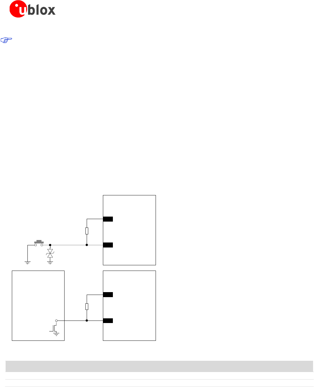
LISA-U1/LISA-H1 series - System Integration Manual
3G.G2-HW-10002-2 Advance Information System description
Page 32 of 116
The PWR_ON pin has high input impedance and is weakly pulled to the high level on the module. Avoid
keeping it floating in a noisy environment. To hold the high logic level stable, the PWR_ON pin must be
connected to a pull-up resistor (e.g. 100 kΩ) biased by the V_BCKP supply pin of the module.
Once the module has turned on, moving the PWR_ON pin has no effect. On the other hand it makes no sense
to keep this pin low once the module has been turned on: if the pin is kept low it will draw unnecessary current.
Following are some typical examples of application circuits to turn the module on using the PWR_ON input pin.
The simplest way to turn on the module is to use a push button that shorts the PWR_ON pin to ground: in this
case the V_BCKP supply pin or the VCC supply of the module can be used to bias the pull-up resistor.
If the PWR_ON input is connected to an external device (e.g. application processor), it is suggested to use an
open drain output on the external device with an external pull-up resistor (e.g. 100 kΩ) biased by the V_BCKP
supply pin of the module.
A push-pull output of an application processor can also be used: in this case the pull-up can be used to pull the
PWR_ON level high when the application processor is switched off. If the high-level voltage of the push-pull
output pin of the application processor is greater than the maximum voltage value as V_BCKP operating range,
the V_BCKP supply cannot be used to bias the pull-up resistor: the supply rail of the application processor or the
VCC supply could be used, but this will increase the V_BCKP (RTC supply) current consumption when the
module is in not-powered mode (VCC supply not present). To avoid an unwanted switch on of the module be
sure to fix the proper level on PWR_ON in all possible scenarios.
LISA-U1/LISA-H1
series
Rext
2V_BCKP
19 PWR_ON
Power-on
push button
ESD
Open
Drain
Output
Application
Processor
LISA-U1/LISA-H1
series
Rext
2V_BCKP
19 PWR_ON
Figure 16: PWR_ON application circuits using a push button and an open drain output of an application processor
Reference
Description
Remarks
Rext
100 kΩ Resistor 0402 5% 0.1 W
External pull-up resistor
ESD
CT0402S14AHSG - EPCOS
Varistor array for ESD protection
Table 11: Example of pull-up resistor and ESD protection for the PWR_ON application circuits
1.6.1.3 Rising edge on RESET_N
The module can be switched on by means of the RESET_N input pin: the RESET_N signal must be forced to the
low level for at least 50 ms and then released from the low level to generate a rising edge that starts the module
power-on sequence.

LISA-U1/LISA-H1 series - System Integration Manual
3G.G2-HW-10002-2 Advance Information System description
Page 33 of 116
The RESET_N input pin can also be used to perform an “external” or “hardware” reset of the module, as
described in the section 1.6.3.
The electrical characteristics of RESET_N are different from the other digital I/O interfaces. The detailed electrical
characteristics are described in the LISA-U1/LISA-H1 series Data Sheet [1].
RESET_N is pulled high to V_BCKP by an integrated pull-up resistor also when the module is in power off mode.
Therefore an external pull-up should not be required on the application board.
The simplest way to switch on the module by means of the RESET_N input pin is to use a push button that
shorts the RESET_N pin to ground: the module will be switched on at the release of the push button, since the
RESET_N will be forced to the high level by the integrated pull-up resistor, generating a rising edge.
If RESET_N is connected to an external device (e.g. an application processor on an application board) an open
drain output can be directly connected without any external pull-up. A push-pull output can be used too: in this
case make sure that the high level voltage of the push-pull circuit is below the maximum voltage value of the
V_BCKP operating range. Make sure to fix the proper level on RESET_N in all possible scenarios, to avoid
unwanted switch-on or reset of the module.
Some typical examples of application circuits using the RESET_N input pin are described in the section 1.6.3.
1.6.1.4 Real Time Clock (RTC) alarm
If a voltage within the operating range is maintained at the VCC pin, the module can be switched on by the RTC
alarm when the RTC system reaches a pre-programmed scheduled time. The RTC system will then initiate the
boot sequence by instructing the Power Management Unit to turn on power. Also included in this setup is an
interrupt signal from the RTC block to indicate to the baseband processor that an RTC event has occurred.
1.6.1.5 Additional considerations
The module is switched on when the voltage rises up to the VCC operating range: the first time that the module
is used, it is switched on in this way. Then, the proper way to switch off the module is by means of the
AT+CPWROFF command. When the module is in power-off mode, i.e. the AT+CPWROFF command has been
sent and a voltage value within the operating range limits is still provided to the VCC pin, the digital input-
output pads of the baseband chipset (i.e. all the digital pins of the module) are locked in tri-state (i.e. floating).
The power down tri-state function isolates the module pins from its environment, when no proper operation of
the outputs can be guaranteed.
The module can be switched on from power-off mode by forcing a proper start-up event (i.e. a falling edge on
the PWR_ON pin, or an RTC alarm). After the detection of a start-up event, all the digital pins of the module are
held in tri-state until all the internal LDO voltage regulators are turned on in a defined power-on sequence. Then,
as described in Figure 17, the baseband core is still held in reset state for a time interval: the internal reset signal
(which is not available on a module pin) is still low and any signal from the module digital interfaces is held in
reset state. The reset state of all the digital pins is reported in the pin description table of the LISA-U1/LISA-H1
series Data Sheet [1]. When the internal signal is released, the configuration of the module interfaces starts:
during this phase any digital pin is set in a proper sequence from the reset state to the default operational
configuration. Finally, the module is fully ready to operate when all interfaces are configured.
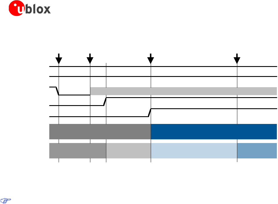
LISA-U1/LISA-H1 series - System Integration Manual
3G.G2-HW-10002-2 Advance Information System description
Page 34 of 116
VCC
V_BCKP
PWR_ON
V_INT
Internal Reset
System State
BB Pads State
Internal Reset → Operational Operational
Tristate / Floating
Internal Reset
OFF
ON
*
Start-up
event
0 ms
~5 ms
~6 ms
~35 ms
~1000 ms
PWR_ON
can be set high
Start of interface
configuration
All interfaces
are configured
Figure 17: LISA power on sequence description (* - the PWR_ON signal state is not relevant during this phase)
The Internal Reset signal is not available on a module pin.
LISA-U1/LISA-H1 series - System Integration Manual
3G.G2-HW-10002-2 Advance Information System description
Page 35 of 116
1.6.2 Module power off
The correct way to switch off LISA-U1/LISA-H1 series modules is by means of +CPWROFF AT command (more
details in u-blox AT Commands Manual [2]): in this way the current parameter settings are saved in the module’s
non-volatile memory and a proper network detach is performed.
An under-voltage shutdown will be done if the VCC supply is removed, but in this case the current parameter
settings are not saved in the module’s non-volatile memory and a proper network detach cannot be performed.
The power off sequence is described in Figure 18. When the +CPWROFF AT command is sent, the module starts
the switch-off routine replying OK on the AT interface: during this phase, the current parameter settings are
saved in the module’s non-volatile memory, a network detach is performed and all module interfaces are
disabled (i.e. the digital pins are locked in tri-state by the module). Since the time to perform a network detach
depends on the network settings, the duration of this phase can differ from the typical value reported in the
following figure. At the end of the switch-off routine, all the digital pins are locked in tri-state by the module
and all the internal LDO voltage regulators except the RTC supply (V_BCKP) are turned off in a defined power
off sequence. The module remains in power off mode as long as a switch on event doesn’t occur (i.e. a falling
edge on the PWR_ON pin or an RTC alarm), and enters not-powered mode if the supply is removed from the
VCC pin.
VCC
V_BCKP
PWR_ON *
V_INT
Internal Reset
System State
BB Pads State Operational
OFF
Tristate / Floating
ON
Operational → Tristate / Floating
AT+CPWROFF
sent to the module
0 ms
~50 ms
~400 ms
OK
replied by the module
Figure 18: LISA Power off sequence description (* - the PWR_ON signal state is not relevant during this phase)
The Internal Reset signal is not available on a module pin.
Tristated pins are always subject to floating caused by noise: to prevent unwanted effects, fix them with
proper pull-up or pull down resistors to stable voltage rails to fix their level when the module is in Power
down state.
LISA-U1/LISA-H1 series - System Integration Manual
3G.G2-HW-10002-2 Advance Information System description
Page 36 of 116
1.6.3 Module reset
The module reset can be performed in one of 2 ways:
Forcing a low level on the RESET_N pin, causing an “external” or “hardware” reset
Via AT command, causing an “internal” or “software” reset
LISA-U1/LISA-H1 series modules can be reset using the RESET_N pin: when the RESET_N pin is forced low for at
least 50 ms, an “external” or “hardware” reset is performed. This causes an asynchronous reset of the entire
module, including the integrated Power Management Unit, except for the RTC internal block: the V_INT
interfaces supply is switched off and all the digital pins are tri-stated, but the V_BCKP supply and the RTC block
are enabled. Forcing an “external” or “hardware” reset, the current parameter settings are not saved in the
module’s non-volatile memory and a proper network detach is not performed.
LISA-U1/LISA-H1 series modules can also be reset by means of the AT+CFUN command (more details in u-blox
AT Commands Manual [2]): in this case an “internal” or “software” reset is performed, causing an asynchronous
reset of the baseband processor, excluding the integrated Power Management Unit and the RTC internal block:
the V_INT interfaces supply is enabled and each digital pin is set in its internal reset state (reported in the pin
description table in the LISA-U1/LISA-H1 series Data Sheet [1]), the V_BCKP supply and the RTC block are
enabled. Forcing an “internal” or “software” reset, the current parameter settings are saved in the module’s
non-volatile memory and a proper network detach is performed.
When RESET_N is released from the low level, the module automatically starts its power on sequence from the
reset state. The same procedure is followed for the module reset via AT command after having performed the
network detach and the parameter saving in non-volatile memory.
The internal reset state of all digital pins is reported in the pin description table in LISA-U1/LISA-H1 series
Data Sheet [1].
Name
Description
Remarks
RESET_N
External reset input
Internal 10 k pull-up to V_BCKP
Table 12: Reset pin
The RESET_N pin ESD rating is 1 kV (contact discharge). A higher protection level could be required if
the line is externally accessible on the application board. A higher protection level can be achieved
mounting an ESD protection (e.g. EPCOS CA05P4S14THSG varistor array) on the line connected to this
pin.
For more details about the general precautions for ESD immunity about RESET_N pin please refer to
chapter 2.5.1.
The electrical characteristics of RESET_N are different from the other digital I/O interfaces. The detailed electrical
characteristics are described in the LISA-U1/LISA-H1 series Data Sheet [1].
RESET_N is pulled high by an integrated 10 k pull-up resistor to V_BCKP. Therefore an external pull-up is not
required on the application board.
Following are some typical examples of application circuits using the RESET_N input pin.
The simplest way to reset the module is to use a push button that shorts the RESET_N pin to ground.
If RESET_N is connected to an external device (e.g. an application processor on an application board) an open
drain output can be directly connected without any external pull-up. A push-pull output can be used too: in this
case make sure that the high level voltage of the push-pull circuit is below the maximum voltage value of the
V_BCKP operating range. To avoid unwanted reset of the module make sure to fix the proper level on RESET_N
in all possible scenarios.
As ESD immunity test precaution, a 47 pF bypass capacitor (e.g. Murata GRM1555C1H470JA01) and a series
ferrite bead (e.g. Murata BLM15HD182SN1) must be added on the RESET_N line pin to avoid a module reset
caused by an electrostatic discharge applied to the application board (for more details, refer to chapter 2.5.1).
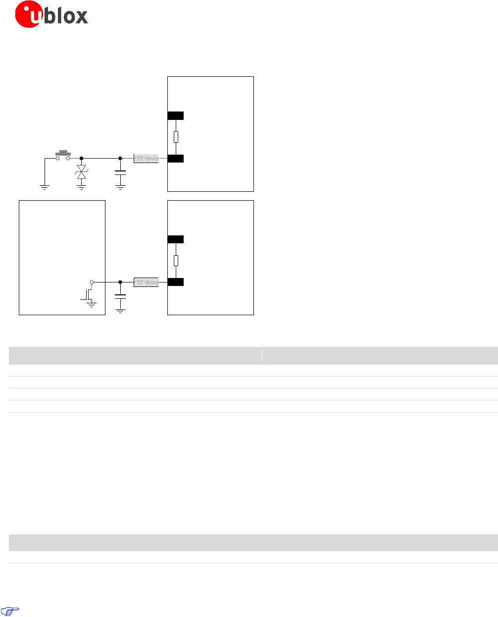
LISA-U1/LISA-H1 series - System Integration Manual
3G.G2-HW-10002-2 Advance Information System description
Page 37 of 116
LISA-U1/LISA-H1
series
2V_BCKP
22 RESET_N
Reset
push button
ESD
Open
Drain
Output
Application
Processor
LISA-U1/LISA-H1
series
2V_BCKP
22 RESET_N
Rint
Rint
FB1
C1
FB2
C2
Figure 19: RESET_N application circuits using a push button and an open drain output of an application processor
Reference
Description
Remarks
ESD
Varistor for ESD protection.
CT0402S14AHSG - EPCOS
C1, C2
47 pF Capacitor Ceramic C0G 0402 5% 50 V
GRM1555C1H470JA01 - Murata
FB1, FB2
Chip Ferrite Bead for Noise/EMI Suppression
BLM15HD182SN1 - Murata
Rint
10 kΩ Resistor 0402 5% 0.1 W
Internal pull-up resistor
Table 13: Example of ESD protection components for the RESET_N application circuit
1.7 RF connection
The ANT pin has 50 nominal characteristic impedance and must be connected to the antenna through a 50
transmission line to allow transmission and reception of radio frequency (RF) signals in the GSM and UMTS
operating bands.
Name
Description
Remarks
ANT
RF antenna
Zo = 50 nominal characteristic impedance.
Table 14: Antenna pin
The ANT port ESD rating is 500 V (contact discharge). A higher protection level could be required if the
line is externally accessible on the application board.
Choose an antenna with optimal radiating characteristics for the best electrical performance and overall module
functionality. An internal antenna, integrated on the application board, or an external antenna, connected to the
application board through a proper 50 connector, can be used. See section 2.4 and section 2.2.1.1 for further
details regarding antenna guidelines.

LISA-U1/LISA-H1 series - System Integration Manual
3G.G2-HW-10002-2 Advance Information System description
Page 38 of 116
The recommendations of the antenna producer for correct installation and deployment (PCB
layout and matching circuitry) must be followed.
If an external antenna is used, the PCB-to-RF-cable transition must be implemented using either a suitable 50
connector, or an RF-signal solder pad (including GND) that is optimized for 50 characteristic impedance.
If antenna supervisor functionality is required, the antenna should have a built in DC diagnostic resistor to
ground to get proper antenna detection functionality (See section 2.4.3).
1.8 (U)SIM interface
A (U)SIM card interface is provided on the SMT pads of the LISA-U1/LISA-H1 series modules: the high-speed
SIM/ME interface is implemented as well as automatic detection of the required SIM supporting voltage.
Both 1.8 V and 3 V SIM types are supported: activation and deactivation with automatic voltage switch from
1.8 V to 3 V is implemented, according to ISO-IEC 7816-3 specifications. The SIM driver supports the PPS
(Protocol and Parameter Selection) procedure for baud-rate selection, according to the values determined by the
SIM Card.
Name
Description
Remarks
VSIM
SIM supply
1.80 V typical or 2.90 V typical
Automatically generated by the module
SIM_CLK
SIM clock
3.25 MHz clock frequency
SIM_IO
SIM data
Open drain, internal 4.7 k pull-up resistor to VSIM
SIM_RST
SIM reset
Table 15: SIM Interface pins
A low capacitance ESD protection (e.g. Infineon ESD8V0L2B-03L or AVX USB0002RP) must be placed
near the SIM card holder on each line (VSIM, SIM_IO, SIM_CLK, SIM_RST). The SIM interface pins ESD
rating is 1 kV (contact discharge): higher protection level is required if the lines are connected to an SIM
card holder/connector, since they are externally accessible on the application board.
For more details about the general precautions for ESD immunity about SIM interface pins please refer
to chapter 2.5.1.
Figure 20 shows an application circuit connecting the LISA module and the SIM card placed in a SIM card holder,
using the SIM detection function provided by GPIO5 pin.
Note that, as defined by ETSI TS 102 221 or ISO/IEC 7816, SIM card contacts assignment is the following:
Contact C1 = VCC (Supply) It must be connected to VSIM
Contact C2 = RST (Reset) It must be connected to SIM_RST
Contact C3 = CLK (Clock) It must be connected to SIM_CLK
Contact C4 = AUX1 (Auxiliary contact for USB interface and other uses) It must be left not connected
Contact C5 = GND (Ground) It must be connected to GND
Contact C6 = VPP (Programming supply) It must be connected to VSIM
Contact C7 = I/O (Data input/output) It must be connected to SIM_IO
Contact C8 = AUX2 (Auxiliary contact for USB interface and other uses) It must be left not connected
A SIM card can have 6 contacts (C1 = VCC, C2 = RST, C3 = CLK, C5 = GND, C6 = VPP, C7 = I/O) or 8 contacts
(providing also the auxiliary contacts C4 = AUX1 and C8 = AUX2). The contacts number depends if additional
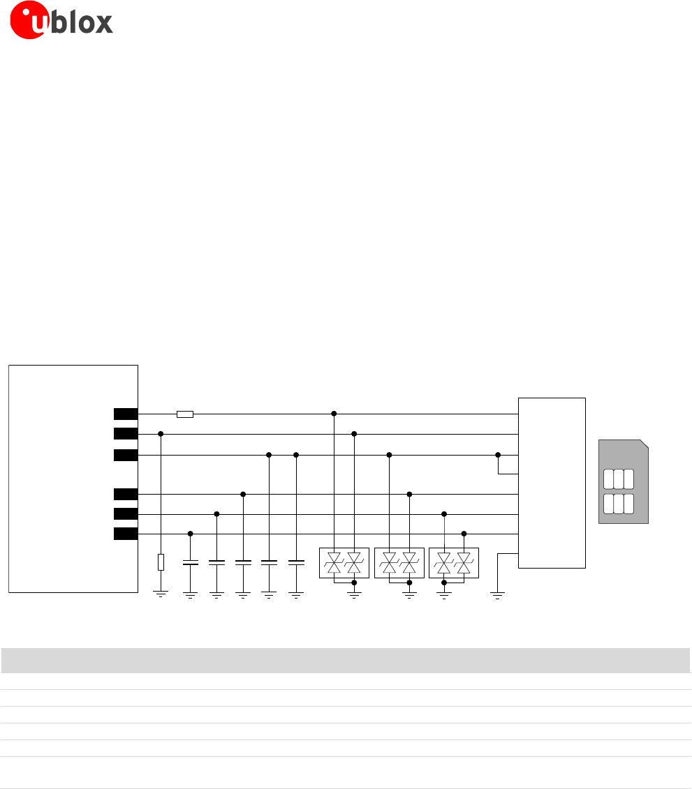
LISA-U1/LISA-H1 series - System Integration Manual
3G.G2-HW-10002-2 Advance Information System description
Page 39 of 116
features, that are not supported by the (U)SIM card interface of the LISA-U1/LISA-H1 series modules, are
provided by the SIM card (contacts C4 = AUX1 and C8 = AUX2 for USB interfaces and other uses).
A SIM card holder can have 6 or 8 positions if a mechanical card presence detector is not provided, or it can
have 6+2 or 8+2 positions if two additional pins for the mechanical card presence detection are provided.
Figure 20 shows an application circuit connecting a LISA-U1/LISA-H1 series module and a SIM card placed in a
SIM card holder with 6+2 pins (as the CCM03-3013LFT R102 connector, produced by C&K Components, which
provides 2 pins for the mechanical card presence detection), using the SIM detection function provided by the
GPIO5 of LISA-U1/LISA-H1 series module. This configuration allows the module to detect if a SIM card is present
in the connector. The SW1 and SW2 pins of the SIM card holder are connected to a normally-open mechanical
switch integrated in the SIM connector. The following cases are available
SIM card not present: the GPIO5 signal is forced low by the pull-down resistor connected to ground (i.e. the
switch integrated in the SIM connector is open)
SIM card present: the GPIO5 signal is forced high by the pull-up resistor connected to V_INT (i.e. the switch
integrated in the SIM connector is closed)
LISA-U1/LISA-H1
series
C1
SIM CARD
HOLDER
CCVCC (C1)
CCVPP (C6)
CCIO (C7)
CCCLK (C3)
CCRST (C2)
GND (C5)
C2 C3 C5
D2 D3
C
5
C
6
C
7
C
1
C
2
C
3
SIM Card
Bottom View
(contacts side)
J1
50
VSIM
48
SIM_IO
47
SIM_CLK
49
SIM_RST
C4
SW1
SW2
4
V_INT
51
GPIO5
R2
R1
D1
Figure 20: SIM interface application circuit
Reference
Description
Part Number - Manufacturer
C1, C2, C3, C4
33 pF Capacitor Ceramic COG 0402 5% 25 V
GRM1555C1H330JZ01 - Murata
C5
100 nF Capacitor Ceramic X7R 0402 10% 16 V
GRM155R71C104KA01 - Murata
D1, D2, D3
ESD Transient Voltage Suppressor
USB0002RP or USB0002DP - AVX
R1
1 kΩ Resistor 0402 5% 0.1 W
RC0402JR-071KL - Yageo Phycomp
R2
470 kΩ Resistor 0402 5% 0.1 W
RC0402JR-07470KL- Yageo Phycomp
J1
SIM Card Holder
Various Manufacturers,
CCM03-3013LFT R102 - C&K Components
Table 16: Example of components for SIM card connection
When connecting the module to an SIM connector, perform the following steps on the application board:
Bypass digital noise via a 100 nF capacitor (e.g. Murata GRM155R71C104K) on the SIM supply (VSIM)
To prevent RF coupling in case the module RF antenna is placed closer than 10 - 30 cm from the SIM card
holder, connect a bypass capacitor of about 22 pF to 47 pF (e.g. Murata GRM1555C1H470J) at each SIM
signal (VSIM, SIM_CLK, SIM_IO, SIM_RST) to ground near the SIM connector
Mount very low capacitance ESD protection (e.g. Infineon ESD8V0L2B-03L or AVX USB0002) near the SIM
card connector

LISA-U1/LISA-H1 series - System Integration Manual
3G.G2-HW-10002-2 Advance Information System description
Page 40 of 116
Limit capacitance and series resistance on each SIM signal to match the requirements for the SIM interface
(27.7 ns is the maximum allowed rise time on the SIM_CLK line, 1.0 µs is the maximum allowed rise time on
the SIM_IO and SIM_RST lines): always route the connections to keep them as short as possible
1.8.1 (U)SIM functionality
The following SIM services are supported:
Abbreviated Dialing Numbers (ADN)
Fixed Dialing Numbers (FDN)
Last Dialed Numbers (LDN)
Service Dialing Numbers (SDN)
USIM Application Toolkit (USAT) is supported.

LISA-U1/LISA-H1 series - System Integration Manual
3G.G2-HW-10002-2 Advance Information System description
Page 41 of 116
1.9 Serial communication
LISA-U1/LISA-H1 series modules provide AT command interface, Packet-Switched / Circuit-Switched Data
communication on the following serial communication interfaces:
One asynchronous serial interface (UART) that provides complete RS-232 functionality conforming to
ITU-T V.24 Recommendation [3], with limited data rate. The UART interface can be used for firmware
upgrade
One Inter Processor Communication (IPC) interface that includes a synchronous SPI-compatible interface,
with maximum data rate of 20 Mb/s
One high-speed USB 2.0 compliant interface, with maximum data rate of 480 Mb/s. The single USB interface
implements 6 logical devices. Each device is a USB communications device class (or USB CDC), that is a
composite Universal Serial Bus device class. The USB interface can be used for firmware upgrade
The LISA-U1/LISA-H1 series modules are designed to operate as an HSPA wireless modem, which represents the
data circuit-terminating equipment (DCE) as described by the ITU-T V.24 Recommendation [3]. A customer
application processor connected to the module through one of the interfaces represents the data terminal
equipment (DTE).
All the interfaces listed above are controlled and operated with:
AT commands according to 3GPP TS 27.007 [4]
AT commands according to 3GPP TS 27.005 [5]
AT commands according to 3GPP TS 27.010 [6]
u-blox AT commands
For the complete list of supported AT commands and their syntax refer to the u-blox AT Commands
Manual [2].
The following serial communication interfaces can be used for firmware upgrade:
The UART interface, using the RxD and TxD lines only
The USB interface, using all the lines provided (VUSB_DET, USB_D+ and USB_D-)
To directly enable PC (or similar) connection to the module for firmware upgrade, provide direct access
on the application board to the VUSB_DET, USB_D+ and USB_D- lines of the module (or to the RxD
and TxD lines). Also provide access to the PWR_ON or the RESET_N pins, or enable the DC supply
connected to the VCC pin to start the module firmware upgrade (see Firmware Update Application Note
[14]).
The following sub-chapters describe the serial interfaces configuration and provide a detailed description of each
interface for the application circuits.
1.9.1 Serial interfaces configuration
UART, USB and SPI/IPC serial interfaces are available as AT command interface and for Packet-Switched / Circuit-
Switched Data communication. The serial interfaces are configured as described in Table 17 (for information
about further settings, please refer to the u-blox AT Commands Manual [2]).

LISA-U1/LISA-H1 series - System Integration Manual
3G.G2-HW-10002-2 Advance Information System description
Page 42 of 116
Interface
AT Settings
Comments
UART interface
Enabled
Multiplexing mode can be enabled by AT+CMUX command providing following channels:
Channel 0: control channel
Channel 1 – 5: AT commands /data connection
Channel 6: GPS tunneling
AT+IPR=115200
Baud rate: 115200 b/s
AT+ICF=0,0
Frame format: 8 bits, no parity, 1 stop bit
AT&K3
HW flow control enabled
AT&S1
DSR line set ON in data mode and set OFF in command mode
AT&D1
Upon an ON-to-OFF transition of DTR, the DCE enters online command state and issues
an OK result code
AT&C1
Circuit 109 changes in accordance with the Carrier detect status; ON if the Carrier is
detected, OFF otherwise
USB interface
Enabled
6 CDCs are available, configured as described in the following list:
USB1: AT commands / data connection
USB2: AT commands / data connection
USB3: AT commands / data connection
USB4: GPS tunneling dedicated port
USB5: 2G trace dedicated port
USB6: 3G trace dedicated port
AT&K3
HW flow control enabled
AT&S1
DSR line set ON in data mode and set OFF in command mode
AT&D1
Upon an ON-to-OFF transition of DTR, the DCE enters online command state and issues
an OK result code
AT&C1
Circuit 109 changes in accordance with the Carrier detect status; ON if the Carrier is
detected, OFF otherwise
SPI interface
Enabled
Multiplexing mode can be enabled by AT+CMUX command providing following channels:
Channel 0: control channel
Channel 1 – 5: AT commands /data connection
Channel 6: GPS tunneling
AT&K3
HW flow control enabled
AT&S1
DSR line set ON in data mode and set OFF in command mode
AT&D1
Upon an ON-to-OFF transition of DTR, the DCE enters online command state and issues
an OK result code
AT&C1
Circuit 109 changes in accordance with the Carrier detect status; ON if the Carrier is
detected, OFF otherwise
Table 17: Default serial interfaces configuration
1.9.2 Asynchronous serial interface (UART)
The UART interface is a 9-wire unbalanced asynchronous serial interface that provides AT commands interface,
PSD and CSD data communication, firmware upgrade.
UART interface provides RS-232 functionality conforming to the ITU-T V.24 Recommendation (more details
available in ITU Recommendation [3]), with CMOS compatible signal levels: 0 V for low data bit or ON state, and
1.8 V for high data bit or OFF state. Two different external voltage translators (Maxim MAX3237E and On
Semiconductor NLSX3018MUTAG) could be used to provide full RS-232 (9 lines) compatible signal levels. The On
Semiconductor chip provides the translation from 1.8 V to 3.3 V, while the Maxim chip provides the necessary
RS-232 compatible signal towards the external connector. If a UART interface with only 5 lines is needed, the
Maxim 13234E voltage level translator can be used. This chip translates the voltage levels from 1.8 V (module
side) to the RS-232 standard. For detailed electrical characteristics refer to the LISA-U1/LISA-H1 series Data Sheet
[1].
The LISA-U1/LISA-H1 series modules are designed to operate as an HSPA wireless modem, which represents the
data circuit-terminating equipment (DCE) as described by the ITU-T V.24 Recommendation [3]. A customer
application processor connected to the module through the UART interface represents the data terminal
equipment (DTE).
LISA-U1/LISA-H1 series - System Integration Manual
3G.G2-HW-10002-2 Advance Information System description
Page 43 of 116
The signal names of the LISA-U1/LISA-H1 series modules UART interface conform to the ITU-T V.24
Recommendation [3].
UART interfaces include the following lines:
Name
Description
Remarks
DSR
Data set ready
Module output
Circuit 107 (Data set ready) in ITU-T V.24
RI
Ring Indicator
Module output
Circuit 125 (Calling indicator) in ITU-T V.24
DCD
Data carrier detect
Module output
Circuit 109 (Data channel received line signal detector) in ITU-T V.24
DTR
Data terminal ready
Module input
Circuit 108/2 (Data terminal ready) in ITU-T V.24
Internal active pull-up to V_INT (1.8 V) enabled.
RTS
Ready to send
Module hardware flow control input
Circuit 105 (Request to send) in ITU-T V.24
Internal active pull-up to V_INT (1.8 V) enabled.
CTS
Clear to send
Module hardware flow control output
Circuit 106 (Ready for sending) in ITU-T V.24
TxD
Transmitted data
Module data input
Circuit 103 (Transmitted data) in ITU-T V.24
Internal active pull-up to V_INT (1.8 V) enabled.
RxD
Received data
Module data output
Circuit 104 (Received data) in ITU-T V.24
GND
Ground
Table 18: UART interface signals
The UART interface pins ESD rating is 1 kV (contact discharge). A higher protection level could be
required if the lines are externally accessible on the application board. A higher protection level can be
achieved mounting an ESD protection (e.g. EPCOS CA05P4S14THSG varistor array) on the lines
connected to these pins.
1.9.2.1 UART features
All flow control handshakes are supported by the UART interface and can be set by appropriate AT commands
(see u-blox AT Commands Manual [2], &K, +IFC, \Q AT commands): hardware flow control (RTS/CTS), software
flow control (XON/XOFF), or none flow control.
Hardware flow control is enabled by default.
The following baud rates can be configured using AT commands:
1200 b/s
2400 b/s
4800 b/s
9600 b/s
19200 b/s
38400 b/s
LISA-U1/LISA-H1 series - System Integration Manual
3G.G2-HW-10002-2 Advance Information System description
Page 44 of 116
57600 b/s
115200 b/s
230400 b/s
460800 b/s
The default baud rate is 115200 b/s. Autobauding is not supported.
The frame format can be:
8N1 (8 data bits, No parity, 1 stop bit)
8E1 (8 data bits, even parity, 1 stop bit)
8O1 (8 data bits, odd parity, 1 stop bit)
8N2 (8 data bits, No parity, 2 stop bits)
7E1 (7 data bits, even parity, 1 stop bit)
7O1 (7 data bits, odd parity, 1 stop bit)
The default frame configuration with fixed baud rate is 8N1, described in the Figure 21.
D0 D1 D2 D3 D4 D5 D6 D7
Start of 1-Byte
transfer
Start Bit
(Always 0)
Possible Start of
next transfer
Stop Bit
(Always 1)
t
bit
= 1/(Baudrate)
Normal Transfer, 8N1
Figure 21: UART default frame format (8N1) description
1.9.2.2 UART signal behavior (AT commands interface case)
See Table 2 for a description of operating modes and states referred to in this section.
At the switch on of the module, before the initialization of the UART interface, as described in the power on
sequence reported in the Figure 17, each pin is first tri-stated and then is set to its relative internal reset state
that is reported in the pin description table in LISA-U1/LISA-H1 series Data Sheet [1]. At the end of the boot
sequence, the UART interface is initialized, the module is by default in active mode and the UART interface is
enabled. The configuration and the behavior of the UART signals after the boot sequence are described below.
For a complete description of data and command mode please refer to u-blox AT Commands Manual
[2].
RxD signal behavior
The module data output line (RxD) is set by default to OFF state (high level) at UART initialization. The module
holds RxD in OFF state until no data is transmitted by the module.

LISA-U1/LISA-H1 series - System Integration Manual
3G.G2-HW-10002-2 Advance Information System description
Page 45 of 116
TxD signal behavior
The module data input line (TxD) is set by default to OFF state (high level) at UART initialization. The TxD line is
then held by the module in the OFF state if the line is not activated by the DTE: an active pull-up is enabled
inside the module on the TxD input.
CTS signal behavior
The module hardware flow control output (CTS line) is set to the ON state (low level) at UART initialization.
If the hardware flow control is enabled (for more details please refer to u-blox AT Commands Manual [2], AT&K,
AT\Q, AT+IFC AT command) the CTS line indicates when the UART interface is enabled (data can be sent and
received): the module drives the CTS line to the ON state or to the OFF state when it is either able or not able to
accept data from the DTE (refer to chapter 1.9.2.3 for the complete description).
If the hardware flow control is not enabled, the CTS line is always held in the ON state after UART initialization.
In case of hardware flow control enabled, when CTS line is ON the UART is enabled and the module is
in active mode. Instead, CTS line to OFF doesn’t necessary mean that the module is in idle-mode, but
only that the UART is not enabled (the module could be forced to stay in active-mode for instance by
USB).
When the power saving configuration is enabled and the hardware flow-control is not implemented in
the DTE/DCE connection, data sent by the DTE can be lost: the first character sent when the module is in
idle-mode won’t be a valid communication character (refer to chapter 1.9.2.3 for the complete
description).
During the MUX mode, the CTS line state is mapped to FCon / FCoff MUX command for flow control
issues outside the power saving configuration while the physical CTS line is still used as a power state
indicator. For more details please refer to Mux Implementation Application Note [15].
RTS signal behavior
The hardware flow control input (RTS line) is set by default to the OFF state (high level) at UART initialization.
The RTS line is then held by the module in the OFF state if the line is not activated by the DTE: an active pull-up
is enabled inside the module on the RTS input.
If the HW flow control is enabled (for more details please refer to u-blox AT Commands Manual [2] AT&K, AT\Q,
AT+IFC command description) the RTS line is monitored by the module to detect permission from the DTE to
send data to the DTE itself. If the RTS line is set to OFF state, any on-going data transmission from the module is
immediately interrupted or any subsequent transmission forbidden until the RTS line changes to ON state.
The DTE must be able to still accept a certain number of characters after the RTS line has been set to
OFF state: the module guarantees the transmission interruption within 2 characters from RTS state
change.
If AT+UPSV=2 is set and HW flow control is disabled, the RTS line is monitored by the module to manage the
power saving configuration:
When an OFF-to-ON transition occurs on the RTS input line, the UART is enabled and the module is forced
to active-mode; after 20 ms from the transition the switch is completed and data can be received without
loss. The module can’t enter idle-mode and the UART is keep enabled as long as the RTS input line is held in
the ON state
If RTS is set to OFF state by the DTE, the module automatically enters idle-mode whenever possible as in the
AT+UPSV=1 configuration (cyclic idle/active mode), but UART is disabled (held in low power mode)
For more details please refer to chapter 1.9.2.3 and u-blox AT Commands Manual [2], AT+UPSV command.

LISA-U1/LISA-H1 series - System Integration Manual
3G.G2-HW-10002-2 Advance Information System description
Page 46 of 116
DSR signal behavior
If AT&S0 is set, the DSR module output line is set by default to ON state (low level) at UART initialization and is
then always held in the ON state.
If AT&S1 is set, the DSR module output line is set by default to OFF state (high level) at UART initialization. The
DSR line is then set to the OFF state when the module is in command mode and is set to the ON state when the
module is in data mode.
The above behavior is valide for both Packet-Switched and Circuit-Switched Data transfer.
DTR signal behavior
The DTR module input line is set by default to OFF state (high level) at UART initialization. The DTR line is then
held by the module in the OFF state if the line is not activated by the DTE: an active pull-up is enabled inside the
module on the DTR input. Module behavior according to DTR status depends on the AT command
configuration (see u-blox AT Commands Manual [2], &D AT command).
DCD signal behavior
If AT&C0 is set, the DCD module output line is set by default to ON state (low level) at UART initialization and is
then always held in the ON state.
If AT&C1 is set, the DCD module output line is set by default to OFF state (high level) at UART initialization. The
DCD line is then set by the module in accordance with the carrier detect status: ON if the carrier is detected, OFF
otherwise. In case of voice call DCD is set to ON state when the call is established. For a data call there are the
following scenarios:
GPRS data communication: Before activating the PPP protocol (data mode) a dial-up application must
provide the ATD*99***<context_number># to the module: with this command the module switches from
command mode to data mode and can accept PPP packets. The module sets the DCD line to the ON state,
then answers with a CONNECT to confirm the ATD*99 command. Please note that the DCD ON is not
related to the context activation but with the data mode
CSD data call: To establish a data call the DTE can send the ATD<number> command to the module which
sets an outgoing data call to a remote modem (or another data module). Data can be transparent (non
reliable) or non transparent (with the reliable RLP protocol). When the remote DCE accepts the data call, the
module DCD line is set to ON and the CONNECT <communication baudrate> string is returned by the
module. At this stage the DTE can send characters through the serial line to the data module which sends
them through the network to the remote DCE attached to a remote DTE
In case of a voice call DCD is set to ON state on all the serial communication interfaces supporting the
AT command interface. (including MUX cirtual channels, if active).
DCD is set to ON during the execution of a command requiring input data from the DTE (all the
commands where a prompt is issued; see u-blox AT Commands Manual [2]). The DCD line is set to ON
state as soon as the switch to binary/text input mode is completed and the prompt is issued; DCD line is
set to OFF as soon as the input mode is interrupted or completed.
RI signal behavior
The RI module output line is set by default to the OFF state (high level) at UART initialization. Then, during an
incoming call, the RI line is switched from OFF state to ON state with a 4:1 duty cycle and a 5 s period (ON for
1 s, OFF for 4 s, see Figure 22), until the DTE attached to the module sends the ATA string and the module
accepts the incoming data call. The RING string sent by the module (DCE) to the serial port at constant time
intervals is not correlated with the switch of the RI line to the ON state.
LISA-U1/LISA-H1 series - System Integration Manual
3G.G2-HW-10002-2 Advance Information System description
Page 47 of 116
Figure 22: RI behavior during an incoming call
The RI line can notify an SMS arrival. When the SMS arrives, the RI line switches from OFF to ON for 1 s (see
Figure 23), if the feature is enabled by the proper AT command (please refer to u-blox AT Commands Manual
[2], AT+CNMI command).
Figure 23: RI behavior at SMS arrival
This behavior allows the DTE to stay in power saving mode until the DCE related event requests service.
In case of SMS arrival, if several events occur coincidently or in quick succession each event triggers the RI line
independently, although the line will not be deactivated between each event. As a result, the RI line may stay to
ON for more than 1 second.
If an incoming call is answered within less than 1 second (with ATA or if autoanswering is set to ATS0=1) than
the RI line will be set to OFF earlier.
As a result:
RI line monitoring can’t be used by the DTE to determine the number of received SMSes.
In case of multiple events (incoming call plus SMS received), the RI line can’t be used to discriminate the
two events, but the DTE must rely on the subsequent URCs and interrogate the DCE with the proper
commands.
1.9.2.3 UART and power-saving
The power saving configuration is controlled by the AT+UPSV command (for the complete description please
refer to u-blox AT Commands Manual [2], AT+UPSV command). When power saving is enabled, the module
automatically enters idle-mode whenever possible, otherwise the active-mode is maintained by the module. The
AT+UPSV command sets the module power saving configuration, but also configures the UART behavior in
relation to the power saving configuration. The conditions for the module entering idle-mode also depend on
the UART power saving configuration.
The different power saving configurations that can be set by the AT+UPSV command are described in the
following subchapters and are summarized in Table 19. For more details on the command description please
refer to u-blox AT commands Manual [2].
SMS arrives
time [s]
0
RI ON
RI OFF
1s
SMS
time [s]
0
RI ON
RI OFF
1s
1s
time [s]
151050
RI ON
RI OFF
Call incomes
1s
time [s]
151050
RI ON
RI OFF
Call incomes
LISA-U1/LISA-H1 series - System Integration Manual
3G.G2-HW-10002-2 Advance Information System description
Page 48 of 116
AT+UPSV
HW flow control
RTS line
Communication during idle mode and wake up
0
Enabled (AT&K3)
ON
Data sent by the DTE will be correctly received by the module.
0
Enabled (AT&K3)
OFF
Data sent by the module will be buffered by the module and will be correctly received by
the DTE when it will be ready to receive data (i.e. RTS line will be ON).
0
Disabled (AT&K0)
ON
Data sent by the DTE will be correctly received by the module.
0
Disabled (AT&K0)
OFF
Data sent by the module will be correctly received by the DTE if it is ready to receive data,
otherwise data will be lost.
1
Enabled (AT&K3)
ON
Data sent by the DTE will be buffered by the DTE and will be correctly received by the
module when active-mode is entered.
1
Enabled (AT&K3)
OFF
Data sent by the module will be buffered by the module and will be correctly received by
the DTE when it is ready to receive data (i.e. RTS line will be ON).
1
Disabled (AT&K0)
ON
If the module is in idle-mode, when a low-to-high transition occurs on the TxD input line,
the module switches from idle-mode to active-mode after 20 ms: this is the “wake up time”
of the module. As a consequence, the first character sent when the module is in idle-mode
(i.e. the wake up character) won’t be a valid communication character because it can’t be
recognized, and the recognition of the subsequent characters is guaranteed only after the
complete wake-up (i.e. after 20 ms).
1
Disabled (AT&K0)
OFF
Data sent by the module will be correctly received by the DTE if it is ready to receive data,
otherwise data will be lost.
2
Enabled (AT&K3)
ON
Not Applicable: HW flow control cannot be enabled with AT+UPSV=2.
2
Enabled (AT&K3)
OFF
Not Applicable: HW flow control cannot be enabled with AT+UPSV=2.
2
Disabled (AT&K0)
ON
The module is forced in active-mode and it can’t enter idle-mode until RTS line is set to OFF
state. When a high-to-low (i.e. OFF-to-ON) transition occurs on the RTS input line, the
module switches from idle-mode to active-mode after 20 ms: this is the “wake up time” of
the module.
2
Disabled (AT&K0)
OFF
When a low-to-high transition occurs on the TxD input line, the UART is re-enabled and if
the module was in idle-mode it switches from idle-mode to active-mode after 20 ms: this is
the “wake up time” of the module. As a consequence, the first character sent when the
module is in idle-mode (i.e. the wake up character) won’t be a valid communication
character because it can’t be recognized, and the recognition of the subsequent characters
is guaranteed only after the complete wake-up (i.e. after 20 ms).
Table 19: UART and power-saving summary
AT+UPSV=0: power saving disabled, fixed active-mode
The module doesn’t enter idle-mode and the CTS line is always held in the ON state after UART initialization. The
UART interface is enabled and data can be received. This is the default configuration.
AT+UPSV=1: power saving enabled, cyclic idle/active mode
The module is allowed to automatically enters idle-mode whenever possible, and periodically wakes up from
idle-mode to active-mode to monitor the paging channel of the current base station (paging block reception), in
accordance to GSM system requirements.
Idle-mode time is fixed by network parameters and can be up to ~2.1 s. When the module is in idle-mode, a
data transmitted by the DTE will be lost if hardware flow control is disabled, otherwise if hardware flow control
is enabled, data will be buffered by the DTE and will be correctly received by the module when active-mode is
entered.
When the module wakes up to active-mode, the UART interface is enabled and data can be received. When a
character is received, it forces the module to stay in the active-mode for a longer time.
The active-mode duration depends by:
Network parameters, related to the time interval for the paging block reception (minimum of ~11 ms)
Time period from the last data received at the serial port during the active-mode: the module doesn’t enter
idle-mode until a timeout expires. This timeout is configurable by the +UPSV AT command, from 40 GSM
frames (~184 ms) up to 65000 GSM frames (300 s). Default value is 2000 GSM frames (~9.2 s)
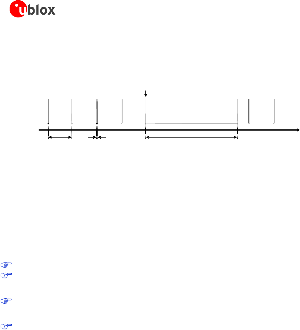
LISA-U1/LISA-H1 series - System Integration Manual
3G.G2-HW-10002-2 Advance Information System description
Page 49 of 116
Every subsequent character received during the active-mode, resets and restarts the timer; hence the active-
mode duration can be extended indefinitely.
The behavior of hardware flow-control output (CTS line) during normal module operations with power-saving
and HW flow control enabled (cyclic idle-mode and active-mode) is illustrated in Figure 24.
Figure 24: CTS behavior with power saving enabled: the CTS line indicates when the module is able (CTS = ON = low level) or
not able (CTS = OFF = high level) to accept data from the DTE and communicate through the UART interface
AT+UPSV=2: power saving enabled and controlled by the RTS line
If the RTS line is set to OFF by the DTE the module is allowed to enter the idle-mode as for UPSV=1 case.
Instead, the UART is disabled as long as RTS line is set to OFF.
If the RTS line is set to ON by the DTE the module is not allowed to enter the idle-mode and the UART is kept
enabled until the RTS line is set to OFF.
When an OFF-to-ON transition occurs on the RTS input line, the UART is re-enabled and the module switches
from idle-mode to active-mode in 20 ms. This configuration can only be enabled with the module HW flow
control disabled.
Since HW flow control is disabled, the CTS line is always set to ON by the module.
When the RTS line is set to OFF by the DTE, the timeout to enter idle-mode from the last data received
at the serial port during the active-mode is the one previously set with the AT+UPSV=1 configuration or
it is the default value.
If the module has to transmit some data (e.g. URC), the UART is temporary enabled even if the RTS line
is set to OFF; UART wake-up in case of RTS line set to OFF is also possible via data reception (as
described in the following).
If the USB is connected and active, the module is forced to stay in active-mode, therefore +UPSV=1 and
+UPSV=2 modes are overruled, but in any case they have effect on the UART behavior (they configure
UART power saving mode (when it is enabled/disabled)).
Wake up from idle-mode to active-mode via data reception
If a data is transmitted by the DTE during the module idle-mode, it will be lost (not correctly received by the
module) in the following cases:
+UPSV=1 with hardware flow control disabled
+UPSV=2 with hardware flow control disabled and RTS line set to OFF
When the module is in idle-mode, the TxD input line of the module is always configured to wake up the module
from idle-mode to active-mode via data reception: when a low-to-high transition occurs on the TxD input line, it
causes the wake-up of the system. The module switches from idle-mode to active-mode in 20 ms from the first
data reception: this is the “wake up time” of the module. As a consequence, the first character sent when the
module is in idle-mode (i.e. the wake up character) won’t be a valid communication character because it can’t be
time [s]
CTS ON
CTS OFF
max ~2.1 s
UART disabled
min ~11 ms
UART enabled
~9.2 s (default)
UART enabled
Data input
time [s]
CTS ON
CTS OFF
max ~2.1 s
UART disabled
min ~11 ms
UART enabled
~9.2 s (default)
UART enabled
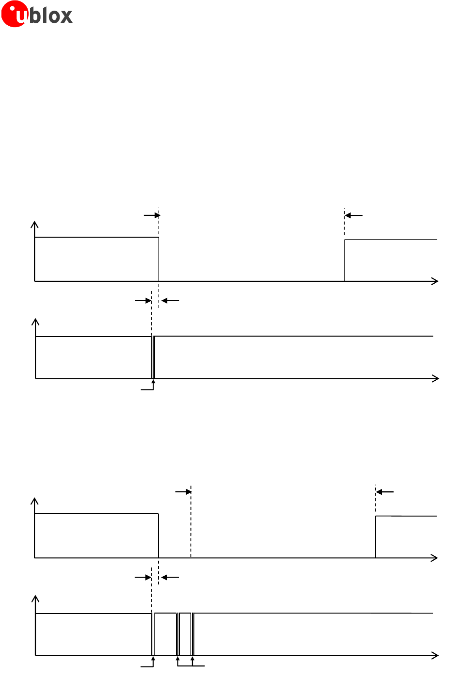
LISA-U1/LISA-H1 series - System Integration Manual
3G.G2-HW-10002-2 Advance Information System description
Page 50 of 116
recognized, and the recognition of the subsequent characters is guaranteed only after the complete wake-up
(i.e. after 20 ms).
Figure 25 and Figure 26 show an example of common scenarios and timing constraints:
HW flow control set in the DCE, and no HW flow control set in the DTE, needed to see the CTS line
changing on DCE
Power saving configuration is active and the timeout from last data received to idle-mode start is set to 2000
frames (AT+UPSV=1,2000)
Figure 25 shows the case where DCE is in idle mode and a wake-up is forced. In this scenario the only character
sent by the DTE is the wake-up character; as a consequence, the DCE will return to idle-mode when the timeout
from last data received expires. (2000 frames without data reception).
CTS OFF
CTS ON
Active mode is held for 2000 GSM frames (~9.2 s)
time
Wake up time: up to 15.6 ms
time
TxD
module
input
Wake up character
Not recognized by DCE
Figure 25: Wake-up via data reception without further communication
Figure 26 shows the case where in addition to the wake-up character further (valid) characters are sent. The
wake up character wakes-up the DCE. The other characters must be sent after the “wake up time” of 20 ms. If
this condition is satisfied, the characters are recognized by the DCE. The DCE is allowed to re-enter idle-mode
after 2000 GSM frames from the latest data reception.
CTS OFF
CTS ON
Active mode is held for 2000 GSM frames (~9.2s)
after the last data received
time
Wake up time: up to 15.6 ms
time
TxD
module
input
Wake up character
Not recognized by DCE
Valid characters
Recognized by DCE
Figure 26: Wake-up via data reception with further communication
LISA-U1/LISA-H1 series - System Integration Manual
3G.G2-HW-10002-2 Advance Information System description
Page 51 of 116
The “wake-up via data reception” feature can’t be disabled.
The “wake-up via data reception” feature can be used in both +UPSV=1 and +UPSV=2 case (when RTS
line is set to OFF).
In command mode, if HW flow control is not implemented by the DTE, the DTE must always send a
dummy “AT” to the module before each command line: the first character will not be ignored if the
module is in active-mode (i.e. the module will reply “OK”), or it will represent the wake up character if
the module is in idle-mode (i.e. the module won’t reply).
No dummy “AT” is required from the DTE during connected-mode since the module continues to be in
active-mode and doesn’t need to be woken-up. Furthermore in data mode a dummy “AT” would affect
the data communication.
1.9.2.4 UART application circuits
Providing the full RS-232 functionality (using the complete V.24 link)
For complete RS-232 functionality conforming to ITU Recommendation [3] in DTE/DCE serial communication, the
complete UART interface of the module (DCE) must be connected to the DTE as described in Figure 27.
LISA-U1/LISA-H1 series
(DCE)
TxD
Application Processor
(DTE)
RxD
RTS
CTS
DTR
DSR
RI
DCD
GND
15 TXD
12 DTR
16 RXD
13 RTS
14 CTS
9DSR
10 RI
11 DCD
GND
Figure 27: Interface application circuit with complete V.24 link in DTE/DCE serial communication

LISA-U1/LISA-H1 series - System Integration Manual
3G.G2-HW-10002-2 Advance Information System description
Page 52 of 116
Providing the TxD, RxD, RTS and CTS lines only (not using the complete V.24 link)
If the functionality of the DSR, DCD, RI and DTR lines is not required in the application, or the lines are not
available, the application circuit described in Figure 28 must be implemented:
Connect the module DTR input line to GND, since the module requires DTR active (low electrical level)
Leave DSR, DCD and RI lines of the module unconnected and floating
LISA-U1/LISA-H1 series
(DCE)
TxD
Application Processor
(DTE)
RxD
RTS
CTS
DTR
DSR
RI
DCD
GND
15 TXD
12 DTR
16 RXD
13 RTS
14 CTS
9DSR
10 RI
11 DCD
GND
Figure 28: UART interface application circuit with partial V.24 link (5-wire) in the DTE/DCE serial communication
If only TxD, RxD, RTS and CTS lines are provided as described in Figure 28 the procedure to enable the power
saving depends on the HW flow-control status. If HW flow-control is enabled (AT&K3, that is the default setting)
the power saving will be activated by AT+UPSV=1. Through this configuration, when the module is in idle-mode,
a data transmitted by the DTE will be buffered by the DTE and will be correctly received by the module when
active-mode is entered.
If the HW flow-control is disabled (AT&K0), the power saving can be enabled by AT+UPSV=2. The module is in
idle-mode until a high-to-low (i.e. OFF-to-ON) transition on the RTS input line will switch the module from
idle-mode to active-mode in 20 ms. The module will be forced in active-mode if the RTS input line is held in the
ON state.
LISA-U1/LISA-H1 series - System Integration Manual
3G.G2-HW-10002-2 Advance Information System description
Page 53 of 116
Providing the TxD and RxD lines only (not using the complete V24 link)
If the functionality of the CTS, RTS, DSR, DCD, RI and DTR lines is not required in the application, or the lines
are not available, the application circuit described in Figure 29 must be implemented:
Connect the module CTS output line to the module RTS input line, since the module requires RTS active
(low electrical level) if HW flow-control is enabled (AT&K3, that is the default setting), and CTS is active (low
electrical level) when the module is in active mode, the UART interface is enabled and the HW flow-control is
enabled
Connect the module DTR input line to GND, since the module requires DTR active (low electrical level)
Leave DSR, DCD and RI lines of the module unconnected and floating
LISA-U1/LISA-H1 series
(DCE)
TxD
Application Processor
(DTE)
RxD
RTS
CTS
DTR
DSR
RI
DCD
GND
15 TXD
12 DTR
16 RXD
13 RTS
14 CTS
9DSR
10 RI
11 DCD
GND
Figure 29: UART interface application circuit with partial V.24 link (3-wire) in the DTE/DCE serial communication
If only TxD and RxD lines are provided as described in Figure 29 and HW flow-control is disabled (AT&K0), the
power saving will be enabled by AT+UPSV=1. The module enters active-mode 20 ms after a low-to-high
transition on the TxD input line; the recognition of the subsequent characters is guaranteed until the module is
in active-mode.
A data delivered by the DTE can be lost using this configuration and the following settings:
o HW flow-control enabled in the module (AT&K3, that is the default setting)
o Module power saving enabled by AT+UPSV=1
o HW flow-control disabled in the DTE
In this case the first character sent when the module is in idle-mode will be a wake-up character and
won’t be a valid communication character (refer to chapter 1.9.1.3 for the complete description).
If power saving is enabled the application circuit with the TxD and RxD lines only is not recommended.
During command mode the DTE must send to the module a wake-up character or a dummy “AT”
before each command line (refer to chapter 1.9.1.3 for the complete description), but during data mode
the wake-up character or the dummy “AT” would affect the data communication.
Additional considerations
If the module USB interface of the is connected to the application processor, it is highly recommended
to provide direct access to RxD, TxD, CTS and RTS lines of the module for execution of firmware
upgrade over UART and for debug purpose: testpoints can be added on the lines to accommodate the
access and a 0 Ω series resistor must be mounted on each line to detach the module pin from any other
connected device. Otherwise, if the USB interface is not connected to the application processor, it is
highly recommended to provide direct access to VUSB_DET, USB_D+, USB_D- lines for execution of
LISA-U1/LISA-H1 series - System Integration Manual
3G.G2-HW-10002-2 Advance Information System description
Page 54 of 116
firmware upgrade over USB and for debug purpose. In both cases, provide as well access to RESET_N
pin, or to the PWR_ON pin, or enable the DC supply connected to the VCC pin to start the module
firmware upgrade (see Firmware Update Application Note [14]).
If the UART interface is not used, all the UART interface pins can be left unconnected, but it is highly
recommended to provide direct access to the RxD, TxD, CTS and RTS lines for execution of firmware
upgrade and for debug purpose.
1.9.3 USB interface
LISA-U1/LISA-H1 series modules provide a high-speed USB interface at 480 Mb/s compliant with the Universal
Serial Bus Revision 2.0 specification [7]. It acts as a USB device and can be connected to any USB host such as a
PC or other Application Processor.
The USB-device shall look for all upper-SW-layers like any other serial device. This means that LISA-U1/LISA-H1
series modules emulate all serial control logical lines.
If the logical DTR line isn't enabled by the USB host, the module doesn’t answer to AT commands by the
USB interface.
Name
Description
Remarks
VUSB_DET
USB detect input
Apply 5 V typical to enable USB
USB_D+
USB Data Line D+
90 Ω nominal differential impedance.
Pull-up or pull-down resistors and external series resistors as
required by the USB 2.0 high-speed specification [7] are part
of the USB pad driver and need not be provided externally.
USB_D-
USB Data Line D-
90 Ω nominal differential impedance.
Pull-up or pull-down resistors and external series resistors as
required by the USB 2.0 high-speed specification [7] are part
of the USB pad driver and need not be provided externally.
Table 20: USB pins
The USB interface pins ESD rating is 1 kV (contact discharge). A higher protection level could be required
if the lines are externally accessible on the application board. A higher protection level can be achieved
mounting a very low capacitance ESD protection (e.g. Tyco Electronics PESD0402-140 ESD protection
device) on the lines connected to these pins.
1.9.3.1 USB features
LISA-U1/LISA-H1 series modules simultaneously support 6 USB CDC (Communications Device Class) that assure
multiple functionalities to the USB physical interface. The 6 available CDCs are configured as described in the
following list:
USB1: AT commands / data connection
USB2: AT commands / data connection
USB3: AT commands / data connection
USB4: GPS tunneling dedicated port
USB5: 2G trace dedicated port
USB6: 3G trace dedicated port
LISA-U1/LISA-H1 series module identifies itself by its VID (Vendor ID) and PID (Product ID) combination, included
in the USB device descriptor. VID and PID of LISA-U1/LISA-H1 series modules are the following:
VID = 0x1546
PID = 0x1101
LISA-U1/LISA-H1 series - System Integration Manual
3G.G2-HW-10002-2 Advance Information System description
Page 55 of 116
If the USB interface of LISA-U1/LISA-H1 series modules is connected to the host before the module switch-on, or
if the module is reset with the USB interface connected to the host, the VID and PID are automatically updated
runtime, after the USB detection. First, VID and PID are the following:
VID = 0x058B
PID = 0x0041
Then, after a time period (~5 s), VID and PID are updated to the following:
VID = 0x1546
PID = 0x1101
If power saving is enabled by AT command (AT+UPSV=1 or AT+UPSV=2), the LISA-U1/LISA-H1 series module
automatically enters the USB suspended state when the device has observed no bus traffic for a specified period
(refer to the Universal Serial Bus Revision 2.0 specification [7]). In suspended state, the module maintains any
internal status as USB device, including its address and configuration. In addition, the module enters the
suspended state when the hub port it is attached to is disabled: this is referred to as USB selective suspend. The
module exits suspend mode when there is bus activity.
LISA-U1/LISA-H1 series module is capable of USB remote wake-up signaling: may request the host to exit
suspend mode or selective suspend by using electrical signaling to indicate remote wake-up. This notifies the
host that it should resume from its suspended mode, if necessary, and service the external event that triggered
the suspended USB device to signal the host. Remote wake-up is accomplished using electrical signaling
described in the Universal Serial Bus Revision 2.0 specification [7].
1.9.3.2 USB application circuit
Since the module acts as a USB device, the USB supply (5.0 V typ.) must be provided to VUSB_DET by the
connected USB host. The USB interface is enabled only when a valid voltage as USB supply is detected by the
VUSB_DET input. Neither the USB interface, nor the whole module is supplied by the VUSB_DET input: the
VUSB_DET senses the USB supply voltage and absorbs few microamperes.
The USB_D+ and USB_D- lines carry the USB serial data and signaling. The lines are used in single ended mode
for relatively low speed signaling handshake, as well as in differential mode for fast signaling and data transfer.
USB pull-up or pull-down resistors on pins USB_D+ and USB_D- as required by the Universal Serial Bus Revision
2.0 specification [7] are part of the USB pad driver and do not need to be externally provided.
External series resistors on pins USB_D+ and USB_D- as required by the Universal Serial Bus Revision 2.0
specification [7] are also integrated: characteristic impedance of USB_D+ and USB_D- lines is specified by the
USB standard. The most important parameter is the differential characteristic impedance applicable for
odd-mode electromagnetic field, which should be as close as possible to 90 differential: signal integrity may
be degraded if the PCB layout is not optimal, especially when the USB signaling lines are very long.
LISA-U1/LISA-H1 series
VBUS
D+
D-
GND
18 VUSB_DET
27 USB_D+
26 USB_D-
GND
C1
USB DEVICE
CONNECTOR
D1 D2 D3
Figure 30: USB Interface application circuit

LISA-U1/LISA-H1 series - System Integration Manual
3G.G2-HW-10002-2 Advance Information System description
Page 56 of 116
Reference
Description
Part Number - Manufacturer
D1, D2, D3
Very Low Capacitance ESD Protection
PESD0402-140 - Tyco Electronics
C2
100 nF Capacitor Ceramic X7R 0402 10% 16 V
GRM155R61A104KA01 - Murata
Table 21: Component for USB application circuit
If the USB interface is not connected to the application processor, it is highly recommended to provide
direct access to the VUSB_DET, USB_D+, USB_D- lines for execution of firmware upgrade over USB
and for debug purpose: testpoints can be added on the lines to accommodate the access. Otherwise, if
the USB interface is connected to the application processor, it is highly recommended to provide direct
access to the RxD, TxD, CTS and RTS lines for execution of firmware upgrade over UART and for debug
purpose. In both cases, provide as well access to RESET_N pin, or to the PWR_ON pin, or enable the
DC supply connected to the VCC pin to start the module firmware upgrade (see Firmware Update
Application Note [14]).
If the USB interface is not used, the USB_D+, USB_D- and VUSB_DET pins can be left unconnected,
but it is highly recommended to provide direct access to the lines for execution of firmware upgrade and
for debug purpose.
1.9.4 SPI interface
SPI is a master-slave protocol: the module runs as an SPI slave, i.e. it accepts AT commands on its SPI interface
without specific configuration. The SPI-compatible synchronous serial interface cannot be used for FW upgrade.
The standard 3-wire SPI interface includes two signals to transmit and receive data (SPI_MOSI and SPI_MISO)
and a clock signal (SPI_SCLK).
LISA-U1/LISA-H1 series modules provide two handshake signals (SPI_MRDY and SPI_SRDY), added to the
standard 3-wire SPI interface, implementing the 5-wire Inter Processor Communication (IPC) interface.
The purpose of the IPC interface is to achieve high speed communication (up to 20 Mb/s) between two
processors following the same IPC specifications: the module baseband processor and an external processor. The
high speed communication is possible only if both sides follow the same Inter Processor Communication (IPC)
specifications.
This interface is designated for high speed HSPA communications and could be necessary to communicate with
an Application Processor which is not equipped with a USB interface.
LISA-U1/LISA-H1 series - System Integration Manual
3G.G2-HW-10002-2 Advance Information System description
Page 57 of 116
Name
Description
Remarks
SPI_MISO
SPI Data Line.
Master Input, Slave Output
Module Output.
Idle high.
Shift data is on rising clock edge, latch on falling edge.
MSB is shifted first.
SPI_MOSI
SPI Data Line.
Master Output, Slave Input
Module Input.
Idle high.
Shift data is on rising clock edge, latch on falling edge.
MSB is shifted first.
Internal active pull-up to V_INT (1.8 V) enabled.
SPI_SCLK
SPI Serial Clock.
Master Output, Slave Input
Module Input.
Idle low.
Up to 20 MHz supported.
Internal active pull-down to GND enabled.
SPI_MRDY
SPI Master Ready to transfer data control line.
Master Output, Slave Input
Module Input.
Idle low.
Internal active pull-down to GND enabled.
SPI_SRDY
SPI Slave Ready to transfer data control line.
Master Input, Slave Output
Module Output.
Idle low.
Table 22: SPI interface signals
The SPI interface pins ESD rating is 1 kV (contact discharge). A higher protection level could be required
if the lines are externally accessible on the application board. A higher protection level can be achieved
mounting an ESD protection (e.g. EPCOS CA05P4S14THSG varistor array) on the lines connected to
these pins.
1.9.4.1 IPC communication protocol overview
The module runs as an SPI slave, i.e. it accepts AT commands on its SPI interface without specific configuration.
The SPI-device shall look for all upper-SW-layers like any other serial device. This means that LISA-U1/LISA-H1
series modules emulate all serial logical lines: the transmission and the reception of the data are similar to an
asynchronous device.
Two additional signals (SPI_MRDY and SPI_SRDY) are added to the SPI lines to communicate the state of
readiness of the two processors: they are used as handshake signals to implement the data flow.
The function of the SPI_MRDY and SPI_SRDY signals is twofold:
For transmitting data the signal indicates to the data receiver that data is available to be transmitted
For receiving data the signal indicates to the transmitter that the receiver is ready to receive data
Due to this setup it is possible to use the control signals as interrupt lines waking up the receiving part when
data is available for transfer. When the handshaking has taken place, the transfer occurs just as if it were a
standard SPI interface without chip select functionality (i.e. one master - one slave setup).
SPI_MRDY is used by the application processor (i.e. the master) to indicate to the module baseband processor
(i.e. the slave) that it is ready to transmit or receive (IPC master ready signal), and can also be used by the
application processor to wake up the module baseband processor if it is in idle mode.
SPI_SRDY line is used by the module baseband processor (i.e. the slave) to indicate to the application processor
(i.e. the master) that it is ready to transmit or receive (IPC slave ready signal), and can also be used by the module
baseband processor to wake up the application processor if it is in hibernation.
If power saving is enabled by AT command (AT+UPSV=1 or AT+UPSV=2), the LISA-U1/LISA-H1 series module
automatically enters idle mode when the master indicates that it is not ready to transmit or receive by the
SPI_MRDY signal, or when the LISA-U1/LISA-H1 series module itself doesn’t transfer data.
LISA-U1/LISA-H1 series - System Integration Manual
3G.G2-HW-10002-2 Advance Information System description
Page 58 of 116
SPI_MRDY
SPI_SRDY
DATA_EXCHANGE
SPI_MOSI
SPI_MISO
Header Data
SPI_SCLK
Figure 31: IPC Data Flow: SPI_MRDY and SPI_SRDY line usage combined with the SPI protocol
For the correct implementation of the SPI protocol, the frame size is known by both sides before a packet
transfer of each packet. The frame is composed by a header with fixed size (always 4 bytes) and a payload with
variable length (must be a multiple of 4 bytes).
The same amount of data is exchanged in both directions simultaneously. Both sides set their readiness lines
(SPI_MRDY / SPI_SRDY) independently when they are ready to transfer data. For the correct transmission of the
data the other side must wait for the activating interrupt to allow the transfer of the other side.
The master starts the clock shortly after SPI_MRDY and SPI_SRDY are set to active. The amount of clocks is
exactly that one of the frame-size to be transferred. The SPI_SRDY line will be set down after the end of the
clock. The SPI_MRDY line is also set inactive with the end of the clock, but in case of a big transfer containing
multiple packets, the SPI_MRDY line stays active.
1.9.4.2 IPC communication examples
In the following, three IPC communication scenarios are described:
Slave initiated data transfer, with a sleeping master
Master initiated data transfer, with a sleeping slave
Slave ended data transfer
Slave initiated transfer with a sleeping master
Figure 32: Data transfer initiated by LISA-U1/LISA-H1 series module (slave), with a sleeping application processor (master)
When the master is sleeping (idle mode), the following actions happen:
1. The slave indicates the master that is ready to send data by activating SPI_SRDY
2. When the master becomes ready to send, it signalizes this by activating SPI_MRDY
3. The master activates the clock and the two processors exchange the communication header and data
SPI_MRDY
SPI_SRDY
DATA EXCHG
2
4
5
Header
Data
Header
3
1
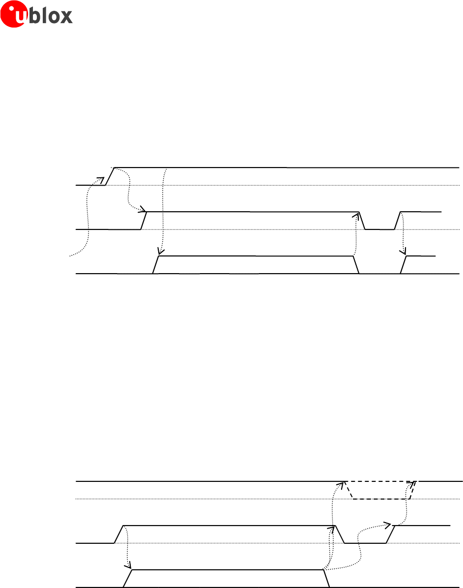
LISA-U1/LISA-H1 series - System Integration Manual
3G.G2-HW-10002-2 Advance Information System description
Page 59 of 116
4. If the data have been exchanged, the slave deactivates SPI_SRDY to process the received information. The
master does not need to de-assert SPI_MRDY as it controls the SPI_SCLK
5. After the preparation, the slave activates again SPI_SRDY and wait for SPI_SCLK activation. When the clock
is active, all the data are transferred without intervention. If there is more data to transfer (flag set in any of
the headers), the process will repeat from step 3
Master initiated transfer with a sleeping slave
Figure 33: Data transfer initiated by application processor (master) with a sleeping LISA-U1/LISA-H1 series module (slave)
When the slave is sleeping (idle mode), the following actions happen:
1. The Master wakes the slave by setting the SPI_MRDY line active
2. As soon as the slave is awake, it signals it by activating SPI_SRDY
3. The master activates the clock and the two processors exchange the communication header and data
4. If the data have been exchanged, the slave deactivates SPI_SRDY to process the received information. The
master does not need to de-assert SPI_MRDY as it controls the SPI_SCLK
5. After the preparation, the slave activates again SPI_SRDY and wait for SPI_SCLK activation. When the clock
is active, all data are transferred without intervention. If there is more data to transfer (flag set in any of the
headers), the process will repeat from step 3
Slave ended transfer
Figure 34: Data transfer terminated and then restarted by LISA-U1/LISA-H1 series module (slave)
Starting from the state where data transfer is ongoing, the following actions will happen:
1. In case of the last transfer, the master will lower its SPI_MRDY line. After the data-transfer is finished the
line must be low. If the slave has already set its SPI_SRDY line, the master must raise its line to initiate the
next transfer (slave-waking-procedure)
2. If the data have been exchanged, the slave will deactivate SPI_SRDY to process the received information.
This is the normal behavior
3. The slave will indicate the master that is ready to send data by activating SPI_SRDY
SPI_MRDY
SPI_SRDY
DATA EXCHG
5
2
1
Header
Data
3
4
SPI_MRDY
SPI_SRDY
DATA EXCHG
1
2
4
5
Header
Data
Header
3
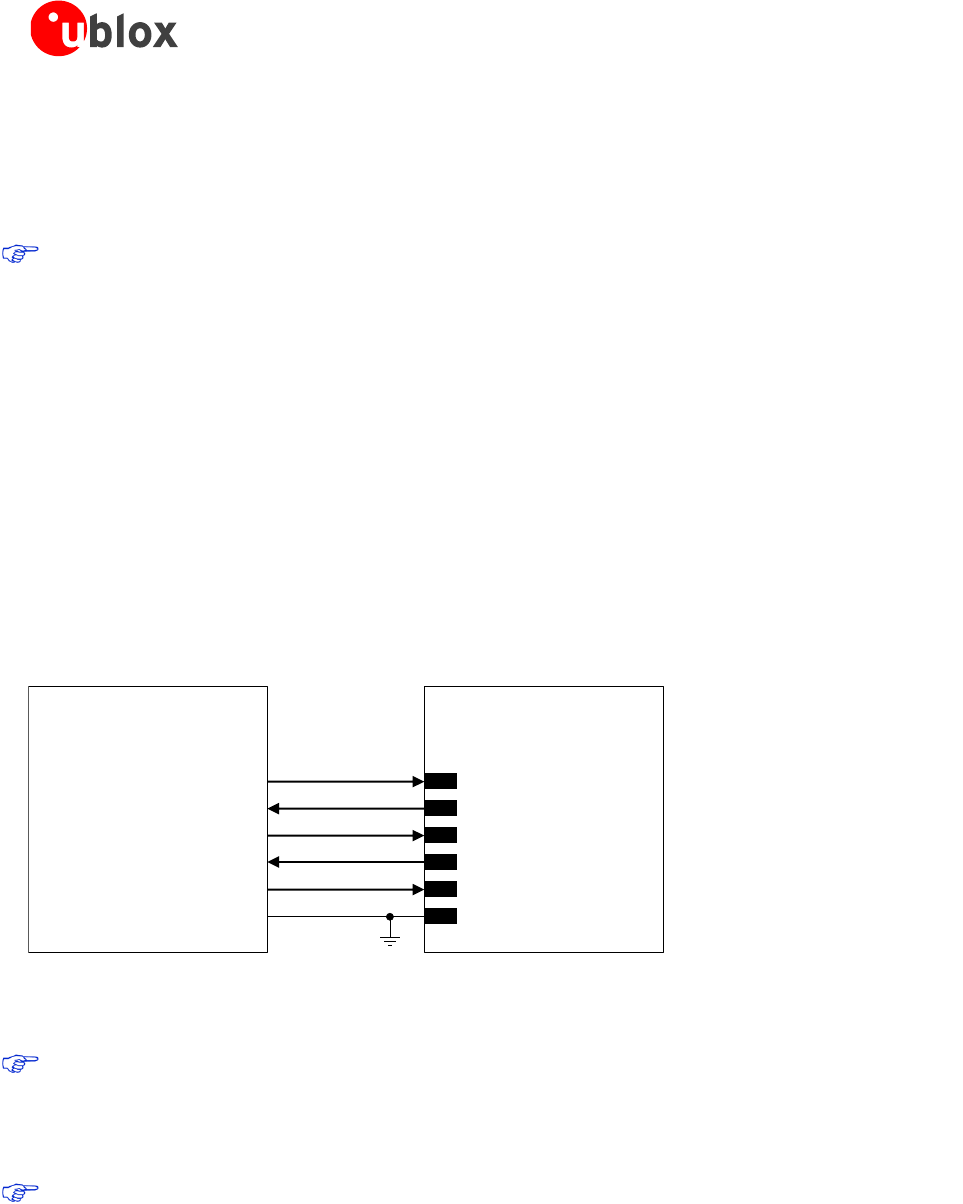
LISA-U1/LISA-H1 series - System Integration Manual
3G.G2-HW-10002-2 Advance Information System description
Page 60 of 116
4. When the master is ready to send, it will signalize this by activating SPI_MRDY. This is optional, when
SPI_MRDY is low before
5. The slave indicates immediately after a transfer termination that it wants to start transmission again. In this
case the slave will raise SPI_SRDY again. The SPI_MRDY line can be either high or low: the master has only
to ensure that the SPI_SRDY change will be detected correctly via interrupt
For more details regarding IPC communication protocol please refer to SPI Application Note [18].
1.9.4.3 IPC application circuit
SPI_MOSI is the data line input for the module since it runs as SPI slave: it must be connected to the data line
output (MOSI) of the application processor that runs as an SPI master.
SPI_MISO is the data line output for the module since it runs as SPI slave: it must be connected to the data line
input (MISO) of the application processor that runs as an SPI master.
SPI_SCLK is the clock input for the module since it runs as SPI slave: it must be connected to the clock line
output (SCLK) of the application processor that runs as an SPI master.
SPI_MRDY is an input for the module able to detect an external interrupt which comes from the application
processor.
SPI_SRDY is an output for the module, and the application processor should be able to detect an external
interrupt which comes from the module on its connected pin.
Signal integrity of the high speed data lines may be degraded if the PCB layout is not optimal, especially when
the SPI lines are very long: keep routing short and minimize parasitic capacitance to preserve signal integrity.
LISA-U1/LISA-H1 series
(SPI slave)
MOSI
Application Processor
(SPI master)
MISO
SCLK
Interrupt
GPIO
GND
56 SPI_MOSI
59 SPI_MRDY
57 SPI_MISO
55 SPI_SCLK
58 SPI_SRDY
GND
Figure 35: IPC Interface application circuit
If direct access to the USB or the UART interfaces of the module is not provided, it is recommended to
provide direct access to the SPI_MOSI, SPI_MISO, SPI_SCLK, SPI_MRDY, SPI_SRDY lines of the
module for debug purpose: testpoints can be added on the lines to accommodate the access and a 0 Ω
series resistor must be mounted on each line to detach the module pin from any other connected
device.
If the SPI/IPC interface is not used, the SPI_MOSI, SPI_MISO, SPI_SCLK, SPI_MRDY, SPI_SRDY pins
can be left unconnected.
1.9.5 MUX Protocol (3GPP 27.010)
The LISA-U1/LISA-H1 series module has a software layer with MUX functionality, 3GPP TS 27.010 Multiplexer
Protocol [6], available on the UART and on the SPI physical link.
This is a data link protocol (layer 2 of OSI model) which uses HDLC-like framing and operates between the
module (DCE) and the application processor (DTE) and allows a number of simultaneous sessions over the used
LISA-U1/LISA-H1 series - System Integration Manual
3G.G2-HW-10002-2 Advance Information System description
Page 61 of 116
physical link (UART or SPI). Each session consists of a stream of bytes transferring various kinds of data such as
SMS, CBS, GPRS, GPS, AT commands in general. This permits, for example, SMS to be transferred to the DTE
when a data connection is in progress.
The following virtual channels are defined:
Channel 0: control channel
Channel 1 – 5: AT commands /data connection
Channel 6: GPS tunneling
For more details please refer to GSM Mux implementation Application Note [15].
1.10 DDC (I2C) interface
1.10.1 Overview
An I2C compatible Display Data Channel (DDC) interface for serial communication is implemented. This interface
is dedicated exclusively to access u-blox GPS receivers.
Name
Description
Remarks
SCL
I2C bus clock line
Open drain. External pull-up required.
SDA
I2C bus data line
Open drain. External pull-up required.
Table 23: DDC pins
The DDC (I2C) interface pins ESD rating is 1 kV (contact discharge). A higher protection level could be
required if the lines are externally accessible on the application board. A higher protection level can be
achieved mounting an ESD protection (e.g. EPCOS CA05P4S14THSG varistor array) on the lines
connected to these pins.
To be compliant to the I2C bus specifications, the module bus interface pads are open drain output and pull up
resistors must be used. Since the pull-up resistors are not mounted on the module, they must be mounted
externally. Resistor values must conform to the I2C bus specifications [8]. If a LISA-U1/LISA-H1 series module is
connected through the DDC bus to a single u-blox GPS receiver only (only one device is connected on the DDC
bus), use a pull-up resistor of 4.7 k. Pull-ups must be connected to a supply voltage of 1.8 V (typical), since this
is the voltage domain of the DDC pins. V_INT digital interfaces supply output can be used to provide 1.8 V for
the pull-ups (for detailed electrical characteristics see the LISA-U1/LISA-H1 series Data Sheet [1]).
DDC Slave-mode operation is not supported, the module can act as master only.
Two lines, serial data (SDA) and serial clock (SCL), carry information on the bus. SCL is used to synchronize data
transfers, and SDA is the data line. Since both lines are open drain outputs, the DDC devices can only drive them
low or leave them open. The pull-up resistor pulls the line up to the supply rail if no DDC device is pulling it
down to GND. If the pull-ups are missing, SCL and SDA lines are undefined and the DDC bus will not work.
The signal shape is defined by the values of the pull-up resistors and the bus capacitance. Long wires on the bus
will increase the capacitance. If the bus capacitance is increased, use pull-up resistors with nominal resistance
value lower than 4.7 k, to match the I2C bus specifications [8].regarding rise and fall times of the signals.
Capacitance and series resistance must be limited on the bus to match the I2C specifications (1.0 µs is
the maximum allowed rise time on the SCL and SDA lines): route connections as short as possible..
If the pins are not used as DDC bus interface, they can be left unconnected.
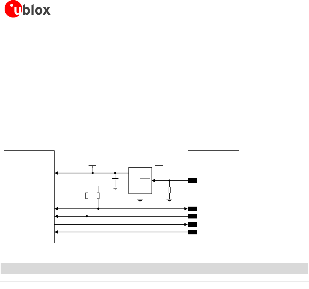
LISA-U1/LISA-H1 series - System Integration Manual
3G.G2-HW-10002-2 Advance Information System description
Page 62 of 116
1.10.2 DDC application circuit
The SDA and SCL lines can be used only to connect the LISA module to a u-blox GPS module: LISA DDC (I2C)
interface is enabled by the +UGPS AT command (for more details refer to u-blox AT Commands Manual [2]).
GPIO2 is automatically driven as an output by the +UGPS AT command to switch-on or to switch-off the u-blox
GPS module, connecting GPIO2 to the active-high enable pin (or the active-low shutdown pin) of the voltage
regulator that supplies the u-blox GPS module on the application board.
GPIO3 is automatically driven as an input by the +UGPS AT command to sense when the u-blox GPS module is
ready to send data.
GPIO4 is automatically driven as an output by the +UGPS AT command to provide a synchronization timing
signal to the u-blox GPS module.
The application circuit for the connection of a LISA-U1/LISA-H1 series wireless module to a u-blox 1.8 V GPS
receiver is illustrated in Figure 36. A pull-down resistor is mounted on the GPIO2 line to avoid a switch on of the
GPS module when the LISA-U1/LISA-H1 series module is in the internal reset state.
LISA-U1/LISA-H1
series
R1
INOUT
GND
GPS LDO
Regulator
SHDN
u-blox
1.8 V GPS receiver
SDA2
SCL2
R2
1V8 1V8
VMAIN1V8
U1
21 GPIO2
SDA
SCL
C1
TxD1
EXTINT0
GPIO3
GPIO4
46
45
23
24
VCC
R3
Figure 36: DDC Application circuit for u-blox 1.8 V GPS receiver
Reference
Description
Part Number - Manufacturer
R1, R2, R3
4.7 kΩ Resistor 0402 5% 0.1 W
RC0402JR-074K7L - Yageo Phycomp
U1
Voltage Regulator for GPS Receiver
See GPS Receiver Hardware Integration Manual
Table 24: Components for DDC application circuit for u-blox 1.8 V GPS receiver
If a 3 V u-blox GPS receiver is used, the SDA, SCL pins and the GPIO2, GPIO3, GPIO4 pins of the
LISA-U1/LISA-H1 series wireless module cannot be directly connected to the 3 V u-blox GPS receiver, since the
pins of the LISA-U1/LISA-H1 series modules aren’t tolerant up to 3 V. An application circuit for the connection of
a LISA-U1/LISA-H1 series wireless module to a u-blox 3.0 V GPS receiver is illustrated in Figure 37. A pull-down
resistor is mounted on the GPIO2 line to avoid a switch on of the GPS module when the LISA-U1/LISA-H1 series
module is in the internal reset state.
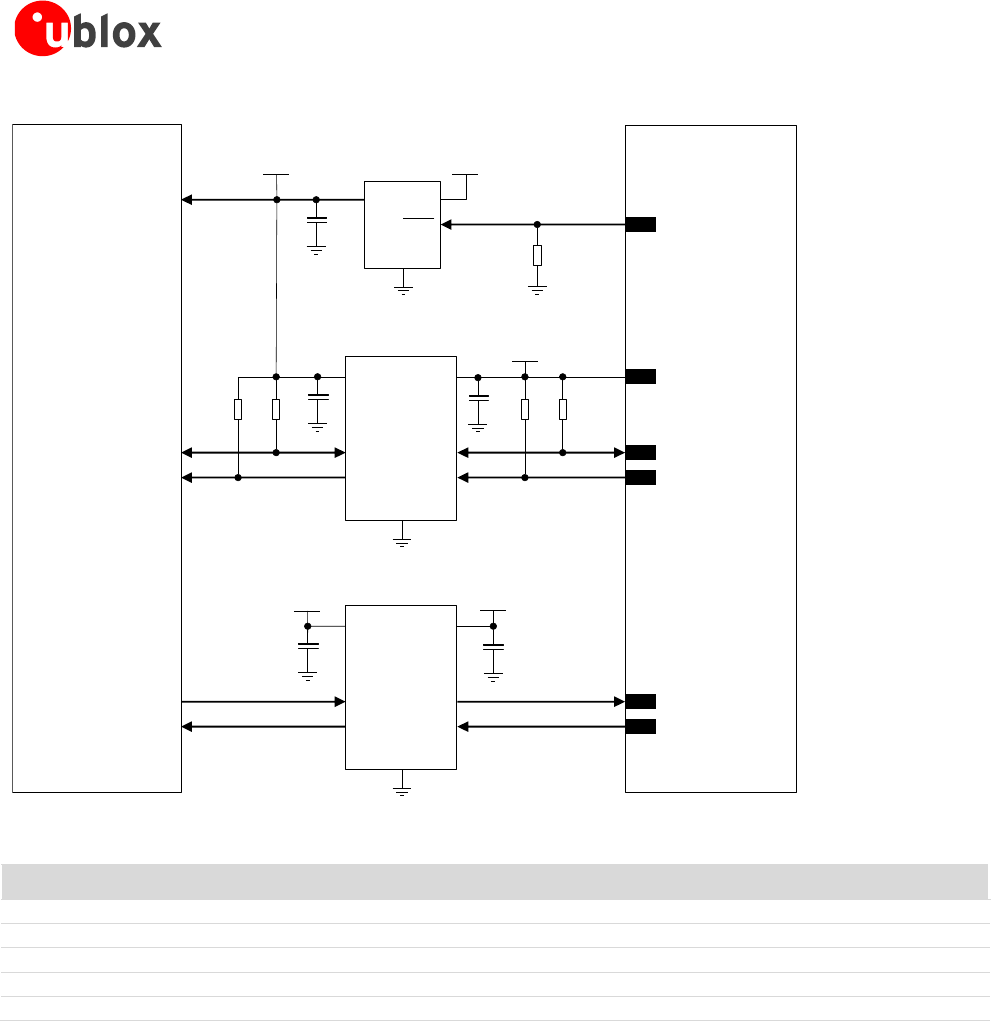
LISA-U1/LISA-H1 series - System Integration Manual
3G.G2-HW-10002-2 Advance Information System description
Page 63 of 116
LISA-U1/LISA-H1
series
R1
INOUT
GND
GPS LDO
Regulator
SHDN
u-blox
3.0 V GPS receiver
R2
VMAIN3V0
U1
21 GPIO2
46 SDA
45 SCL
R4 R5
1V8
SDA1 SDA2
GND
U2
SCL1SCL2
VREF1VREF2
I2C-bus
Bidirectional
Voltage Translator
21 V_INT
C1
C2 C3
R3
23 GPIO3
24 GPIO4
1V8
A1 B1
GND
U3
A2B2
VCCAVCCB
Generic
Bidirectional
Voltage Translator
C4 C5
3V0
SDA2
SCL2
TxD1
EXTINT0
VCC
Figure 37: DDC Application circuit for u-blox 3.0 V GPS receiver
Reference
Description
Part Number - Manufacturer
R1, R2, R3, R4, R5
4.7 kΩ Resistor 0402 5% 0.1 W
RC0402JR-074K7L - Yageo Phycomp
C2, C3, C4, C5
100 nF Capacitor Ceramic X5R 0402 10% 10V
GRM155R71C104KA01 - Murata
U1
Voltage Regulator for GPS Receiver
See GPS Receiver Hardware Integration Manual
U2
I2C-bus Bidirectional Voltage Translator
PCA9306DCURG4 - Texas Instruments
U3
Generic Bidirectional Voltage Translator
TXB0104PWR - Texas Instruments
Table 25: Components for DDC application circuit for u-blox 3.0 V GPS receiver
1.11 Audio Interface (LISA-U120 and LISA-U130 only)
LISA-U120 and LISA-U130 modules provide analog and digital audio interfaces:
One differential analog audio input (microphone input)
One differential analog audio output (speaker output)
One 4-wire I2S digital audio interface: input and output
Audio signal routing can be controlled by the dedicated AT command +USPM (refer to u-blox AT Commands
Manual [2]). This command allows setting the audio path mode, composed by the uplink audio path and the
downlink audio path.

LISA-U1/LISA-H1 series - System Integration Manual
3G.G2-HW-10002-2 Advance Information System description
Page 64 of 116
Each uplink path mode defines the physical input (i.e. the analog or the digital audio input) and the set of
parameters to process the uplink audio signal (uplink gains, uplink digital filters, echo canceller parameters). For
example the “Headset microphone” uplink path uses the differential analog audio input with the default
parameters for the headset profile.
Each downlink path mode defines the physical output (i.e. the analog or the digital audio output) and the set of
parameters to process the downlink audio signal (downlink gains, downlink digital filters and sidetone). For
example the “Mono headset” downlink path uses the differential analog audio output with the default
parameters for the headset profile.
The set of parameters to process the uplink or the downlink audio signal can be changed with dedicated AT
commands for each uplink or downlink path and then stored in two profiles in the non volatile memory (refer to
u-blox AT Commands Manual [2] for Audio parameters tuning commands).
1.11.1 Analog Audio interface
1.11.1.1 Uplink path (differential analog audio input)
The pins related to the differential analog audio input are:
MIC_P / MIC_N: Differential analog audio signal inputs (positive/negative). These two pins are provided with
internal series 100 nF capacitors for DC blocking that connect the module pads to the differential input of a
Low Noise Amplifier. The LNA output is internally connected to the digital processing system by an
integrated sigma-delta analog-to-digital converter
The analog audio input is selected when the parameter <main_uplink> in AT+USPM command is set to
“Headset microphone”, “Handset microphone” or “Hands-free microphone”: the uplink analog path profiles
use the same physical input but have different sets of audio parameters (for more details please refer to u-blox
AT Commands Manual [2], AT+USPM, AT+UMGC, AT+UUBF, AT+UHFP commands).
There is no microphone supply pin available on the module: an external low noise LDO voltage regulator should
be added to provide a proper supply for a microphone.
Detailed electrical characteristics of the differential analog audio input can be found in the LISA-U1/LISA-H1
series Data Sheet [1].
1.11.1.2 Downlink path (differential analog audio output)
The pins related to the differential analog audio output are:
SPK_N / SPK_P: Differential analog audio signal output (positive/negative). These two pins are internally
directly connected to the differential output of a low power audio amplifier, for which the input is internally
connected to the digital processing system by to an integrated digital-to-analog converter.
The analog audio output is selected when the parameter <main_downlink> in AT+USPM command is set to
“Normal earpiece”, “Mono headset” or “Loudspeaker”: the downlink analog path profiles use the same
physical output but have different sets of audio parameters (for more details please refer to u-blox AT
Commands Manual [2], AT+USPM, AT+USGC, AT+UDBF, AT+USTN commands).
The differential analog audio output can be directly connected to a headset earpiece or handset earpiece but is
not able to drive an 8 speaker.
Detailed electrical characteristics of the high power differential audio output can be found in the
LISA-U1/LISA-H1 series Data Sheet [1].
Warning: excessive sound pressure from headphones can cause hearing loss.
LISA-U1/LISA-H1 series - System Integration Manual
3G.G2-HW-10002-2 Advance Information System description
Page 65 of 116
Table 26 lists the signals related to analog audio functions.
Name
Description
Remarks
MIC_P
Differential analog audio input (Positive)
Shared for all uplink analog path modes: handset, headset,
hands-free mode.
Internal DC blocking capacitor.
MIC_N
Differential analog audio input (Negative)
Shared for all uplink analog path modes: handset, headset,
hands-free mode.
Internal DC blocking capacitor.
SPK_P
Differential analog audio output (Positive)
Shared for all uplink analog path modes: earpiece, headset,
loudspeaker mode.
SPK_N
Differential analog audio output (Negative)
Shared for all uplink analog path modes: earpiece, headset,
loudspeaker mode.
Table 26: Analog Audio Signal Pins
The audio pins ESD rating is 1 kV (contact discharge). A higher protection level could be required if the
lines are externally accessible on the application board. A higher protection level can be achieved
mounting an ESD protection (e.g. EPCOS CA05P4S14THSG varistor array) on the lines connected to
these pins.
All corresponding differential audio lines must be routed in pairs, be embedded in GND (have the
ground lines as close as possible to the audio lines), and maintain distance from noisy lines such as VCC
and from components such as switching regulators.
If the audio pins are not used, they can be left unconnected on the application board.
1.11.1.3 Headset mode
Headset mode is the default audio operating mode of the LISA-U120 and LISA-U130 modules. The headset
profile is configured when the uplink audio path is set to “Headset microphone” and the downlink audio path is
set to “Mono headset” (refer to u-blox AT Commands Manual [2]: AT+USPM command: <main_uplink>,
<main_downlink> parameters):
Headset microphone must be connected to the module differential input MIC_P / MIC_N
Headset receiver must be connected to the module differential output SPK_P / SPK_N
Figure 38 shows an example of an application circuit connecting a headset (with a 2.2 k electret microphone
and a 32 receiver) to the LISA-U120 and LISA-U130 modules, with an external low noise LDO voltage
regulator to provide a proper supply for the microphone.
Mount an 82 nH series inductor (e.g. Murata LQG15HS82NJ02) on each microphone line, and a 27 pF
bypass capacitor (e.g. Murata GRM1555C1H270J) on all audio lines to minimize RF coupling and TDMA
noise.
The physical width of the audio outputs lines on the application board must be wide enough to
minimize series resistance.
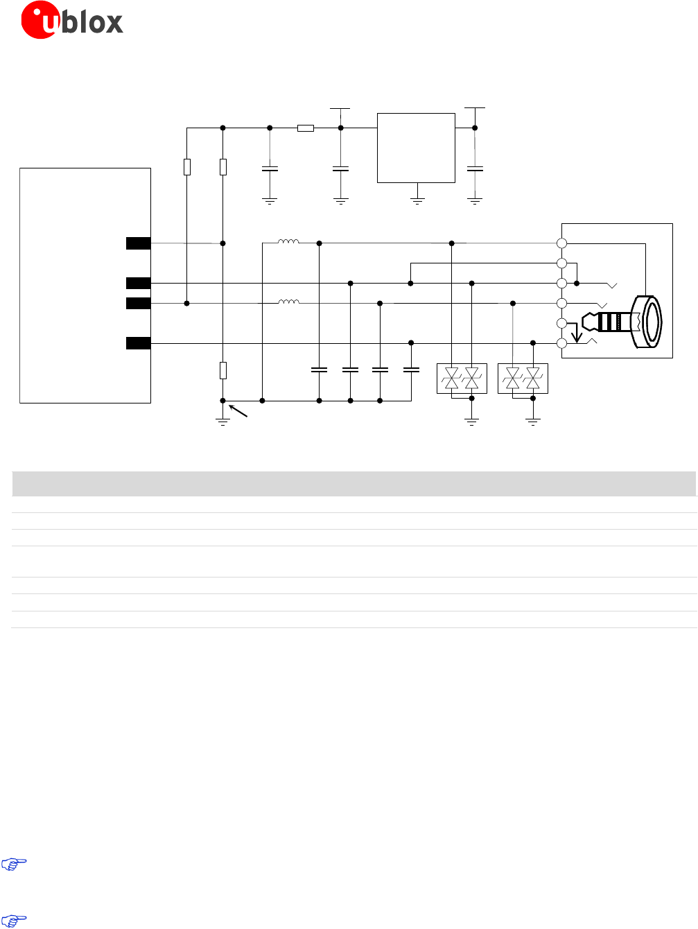
LISA-U1/LISA-H1 series - System Integration Manual
3G.G2-HW-10002-2 Advance Information System description
Page 66 of 116
LISA-U120/U130
C2 C3 C4
J1
2
5
3
4
6
1
L2
54
SPK_N
53
SPK_P
39
MIC_N
40
MIC_P
D1
AUDIO HEADSET
CONNECTOR
D2
INOUT
GND
Low Noise
LDO Regulator VMAIN
U1
R4
R1
C6
R3R2 C5
2V5
Sense lines connected to GND in one star point
L1
C1
C7
Figure 38: Headset mode application circuit
Reference
Description
Part Number - Manufacturer
C1, C2, C3, C4
27 pF Capacitor Ceramic COG 0402 5% 25 V
GRM1555C1H270JA01 - Murata
C5, C6, C7
10 µF Capacitor Ceramic X5R 0603 20% 6.3 V
GRM188R60J106ME47 - Murata
D1, D2
Low Capacitance ESD Protection
USB0002RP or USB0002DP - AVX
L1, L2
82 nH Multilayer inductor 0402
(self resonance frequency ~1 GHz)
LQG15HS82NJ02 - Murata
J1
Audio Headset 2.5 mm Jack Connector
SJ1-42535TS-SMT – CUI, Inc.
R1, R2, R3, R4
2.2 kΩ Resistor 0402 5% 0.1 W
RC0402JR-072K2L - Yageo Phycomp
U1
Low Noise LDO Linear Regulator 2.5 V 300 mA
LT1962EMS8-2.5#PBF- Linear Technology
Table 27: Example of components for headset jack connection
1.11.1.4 Handset mode
The handset profile is configured when the uplink audio path is set to “Handset microphone” and the downlink
audio path is set to “Normal earpiece” (refer to u-blox AT commands manual [2]: AT+USPM command:
<main_uplink>, <main_downlink> parameters):
Handset microphone must be connected to the module differential input MIC_P / MIC_N
Handset receiver must be connected to the module differential output SPK_P / SPK_N
Figure 39 shows an example of an application circuit connecting a handset (with a 2.2 k electret microphone
and a 32 receiver) to the LISA-U120 and LISA-U130 modules, with an external low noise LDO voltage
regulator to provide a proper supply for the microphone.
Mount an 82 nH series inductor (e.g. Murata LQG15HS82NJ02) on each microphone line and a 27 pF
bypass capacitor (e.g. Murata GRM1555C1H270J) on all audio lines to minimize RF coupling and TDMA
noise.
The physical width of the audio outputs lines on the application board must be wide enough to
minimize series resistance.
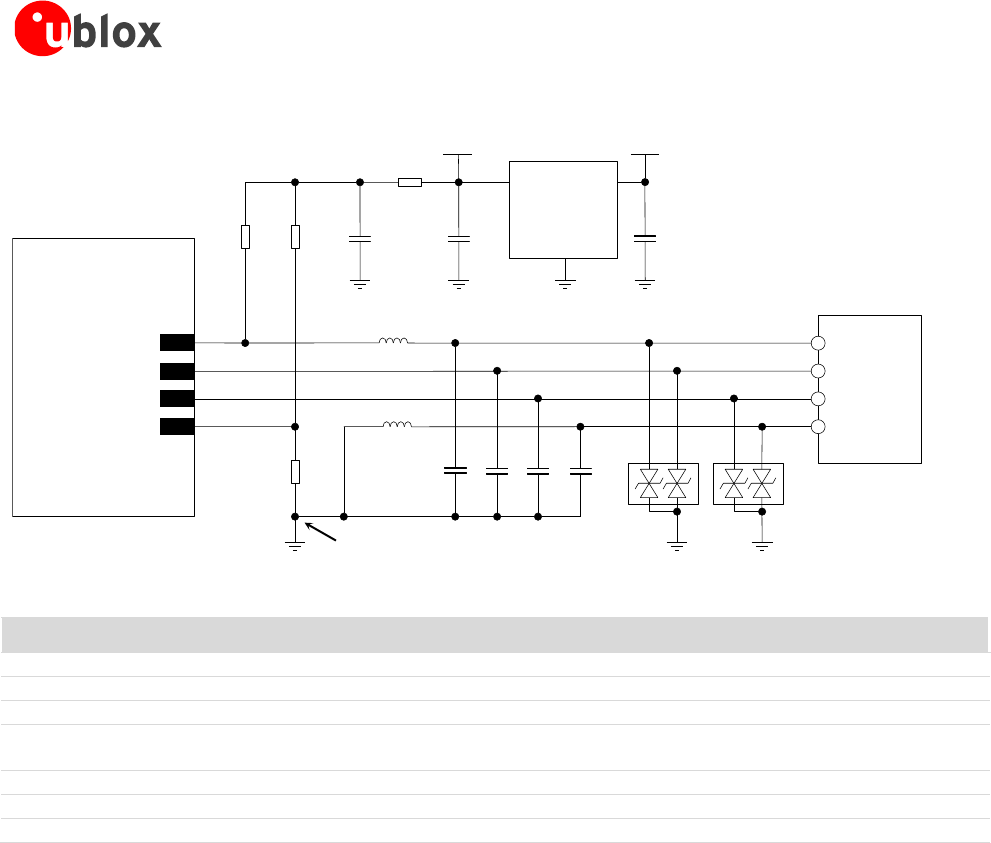
LISA-U1/LISA-H1 series - System Integration Manual
3G.G2-HW-10002-2 Advance Information System description
Page 67 of 116
LISA-U120/U130
C1 C2 C3 J1
4
3
2
1
L1
53
SPK_P
54
SPK_N
40
MIC_P
39
MIC_N
D1
AUDIO
HANDSET
CONNECTOR
D2
INOUT
GND
Low Noise
LDO Regulator
U1
R4
R1
C6
R3R2 C5
2V5
Sense lines connected to GND in one star point
C4
L2
VMAIN
C7
Figure 39: Handset mode application circuit
Reference
Description
Part Number - Manufacturer
C1, C2, C3, C4
27 pF Capacitor Ceramic COG 0402 5% 25 V
GRM1555C1H270JA01 - Murata
C5, C6, C7
10 µF Capacitor Ceramic X5R 0603 20% 6.3 V
GRM188R60J106ME47 - Murata
D1, D2
Low Capacitance ESD Protection
USB0002RP or USB0002DP - AVX
L1, L2
82nH Multilayer inductor 0402
(self resonance frequency ~1 GHz)
LQG15HS82NJ02 - Murata
J1
Audio Handset Jack Connector, 4Ckt (4P4C)
52018-4416 - Molex
R1, R2, R3, R4
2.2 kΩ Resistor 0402 5% 0.1 W
RC0402JR-072K2L - Yageo Phycomp
U1
Low Noise LDO Linear Regulator 2.5 V 300 mA
LT1962EMS8-2.5#PBF- Linear Technology
Table 28: Example of components for handset connection
1.11.1.5 Hands-free mode
The hands-free profile is configured when the uplink audio path is set to “Hands-free microphone” and the
downlink audio path is set to “Loudspeaker” (refer to u-blox AT commands manual [2]: AT+USPM command:
<main_uplink>, <main_downlink> parameters):
Hands-free microphone signal must be connected to the module differential input MIC_P / MIC_N
High power loudspeaker must be connected to the output of an external audio amplifier, for which the
input must be connected to the module differential output SPK_P / SPK_N
The module differential analog audio output is not able to drive an 8 speaker: an external audio amplifier
must be provided on the application board to amplify the low power audio signal provided by the module
differential output SPK_P / SPK_N.
Hands-free functionality is implemented using appropriate digital signal processing algorithms for voice-band
handling (echo canceller and automatic gain control), managed via software (refer to u-blox AT commands
manual [2], AT+UHFP command).
Figure 39 shows an example of an application circuit connecting a 2.2 k electret microphone and an 8
speaker to the LISA-U120 and LISA-U130 modules, with an external low noise LDO voltage regulator to provide
a proper supply for the microphone and with an external audio amplifier to amplify the low power audio signal
provided by the module differential output.
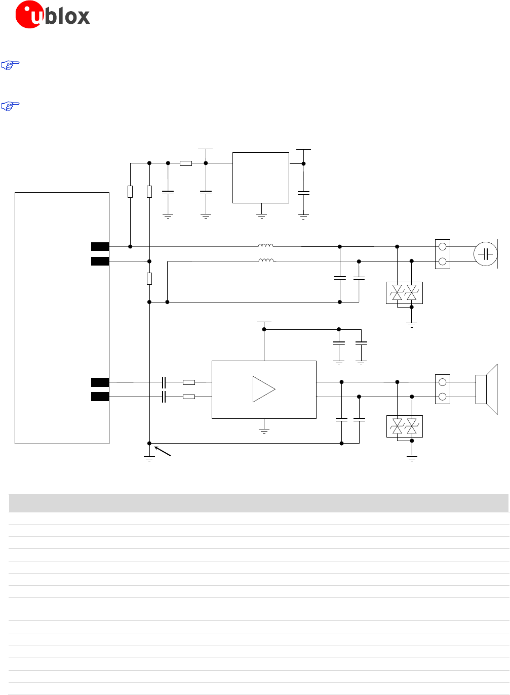
LISA-U1/LISA-H1 series - System Integration Manual
3G.G2-HW-10002-2 Advance Information System description
Page 68 of 116
Mount an 82 nH series inductor (e.g. Murata LQG15HS82NJ02) on each microphone line and a 27 pF
bypass capacitor (e.g. Murata GRM1555C1H270J) on all audio lines to minimize RF coupling and TDMA
noise.
The physical width of the audio outputs lines on the application board must be wide enough to
minimize series resistance.
C1 C2
C3
L1
39
MIC_N
53
SPK_P
40
MIC_P
54
SPK_N
D1
Microphone
Connector
D2
INOUT
GND
Low Noise
LDO Regulator
U1
R4
R1
C6
R3R2 C5
2V5
Sense lines connected to GND in one star point
C4
SPK
L2
MIC
Speaker
Connector
OUT+
IN+
GND
VMAIN
U2
OUT-
IN-
C8
C9
R5
R6
VDD
C11C10
LISA-U120/U130
Audio
Amplifier
J1
J2
VMAIN
C7
Figure 40: Hands-free mode application circuit
Reference
Description
Part Number - Manufacturer
C1, C2, C3, C4
27 pF Capacitor Ceramic COG 0402 5% 25 V
GRM1555C1H270JZ01 - Murata
C5, C6, C7, C10
10 µF Capacitor Ceramic X5R 0603 20% 6.3 V
GRM188R60J106ME47 - Murata
C8, C9
47 nF Capacitor Ceramic X7R 0402 10% 16V
GRM155R71C473KA01 - Murata
C11
100 nF Capacitor Ceramic X5R 0402 10% 10V
GRM155R71C104KA01 - Murata
D1, D2
Low Capacitance ESD Protection
USB0002RP or USB0002DP - AVX
J1
Microphone Connector
J2
Speaker Connector
L1, L2
82nH Multilayer inductor 0402
(self resonance frequency ~1 GHz)
LQG15HS82NJ02 - Murata
MIC
2.2 k Electret Microphone
R1, R2, R3, R4
2.2 kΩ Resistor 0402 5% 0.1 W
RC0402JR-072K2L - Yageo Phycomp
R5, R6
0 Ω Resistor 0402 5% 0.1 W
RC0402JR-070RL - Yageo Phycomp
SPK
8 Loudspeaker
U1
Low Noise LDO Linear Regulator 2.5 V 300 mA
LT1962EMS8-2.5#PBF- Linear Technology
U2
Filter-less Mono 2.8 W Class-D Audio Amplifier
SSM2305CPZ - Analog Devices
Table 29: Example of components for hands-free connection

LISA-U1/LISA-H1 series - System Integration Manual
3G.G2-HW-10002-2 Advance Information System description
Page 69 of 116
1.11.1.6 Connection to an external analog audio device
The differential analog audio input / output can be used to connect the module to an external analog audio
device. Audio devices with a differential analog input / output are preferable, as they are more immune to
external disturbances.
If the external analog audio device is provided with a differential analog audio input, the SPK_P / SPK_N
balanced output of the module must be connected to the differential input of the external audio device through
a DC-block 10 µF series capacitor (e.g. Murata GRM188R60J106M) to decouple the bias present at the module
output (see SPK_P / SPK_N common mode output voltage in the LISA-U1/LISA-H1 series Data Sheet [1]). Use a
suitable power-on sequence to avoid audio bump due to charging of the capacitor: the final audio stage should
be always enabled as last one.
If the external analog audio device is provided with a single ended analog audio input, a proper differential to
single ended circuit must be inserted from the SPK_P / SPK_N balanced output of the module to the single
ended input of the external audio device. A simple application circuit is described in Figure 41: 10 µF series
capacitors (e.g. Murata GRM188R60J106M) are provided to decouple the bias present at the module output,
and a voltage divider is provided to properly adapt the signal level from the module output to the external audio
device input.
The DC-block series capacitor acts as high-pass filter for audio signals, with cut-off frequency depending on both
the values of capacitor and on the input impedance of the external audio device. For example: in case of
differential input impedance of 600 , the two 10 µF capacitors will set the -3 dB cut-off frequency to 53 Hz,
while for single ended connection to 600 external device, the cut-off frequency with just the single 10 µF
capacitor will be 103 Hz. In both cases the high-pass filter has a low enough cut-off to not impact the audio
signal frequency response.
The signal levels can be adapted by setting gain using AT commands, but additional circuitry must be inserted if
the SPK_P / SPK_N output level of the module is too high for the input of the audio device.
If the external analog audio device is provided with a differential analog audio output, the MIC_P / MIC_N
balanced input of the module must be connected directly to the differential output of the external audio device.
Series capacitors are not needed since MIC_P / MIC_N pins are provided with internal 100 nF capacitors for DC
blocking (see LISA-U1 series Data Sheet [1]).
If the external analog audio device is provided with a single ended analog audio output, a proper single ended to
differential circuit has to be inserted from the single ended output of the external audio device to the
MIC_P / MIC_N balanced input of the module. A simple application circuit is described in Figure 41: a voltage
divider is provided to properly adapt the signal level from the external audio device output to the module input.
The signal levels can be adapted by setting gain using AT commands, but additional circuitry must be inserted if
the output level of the audio device is too high for MIC_P / MIC_N. Please refer to Figure 41 for the application
circuits.
To enable the audio path corresponding to the differential analog audio input / output, please refer to
u-blox AT Commands Manual [2]: AT+USPM command.
To tune audio levels for the external device please refer to u-blox AT Commands Manual [2] (AT+USGC,
AT+UMGC commands).
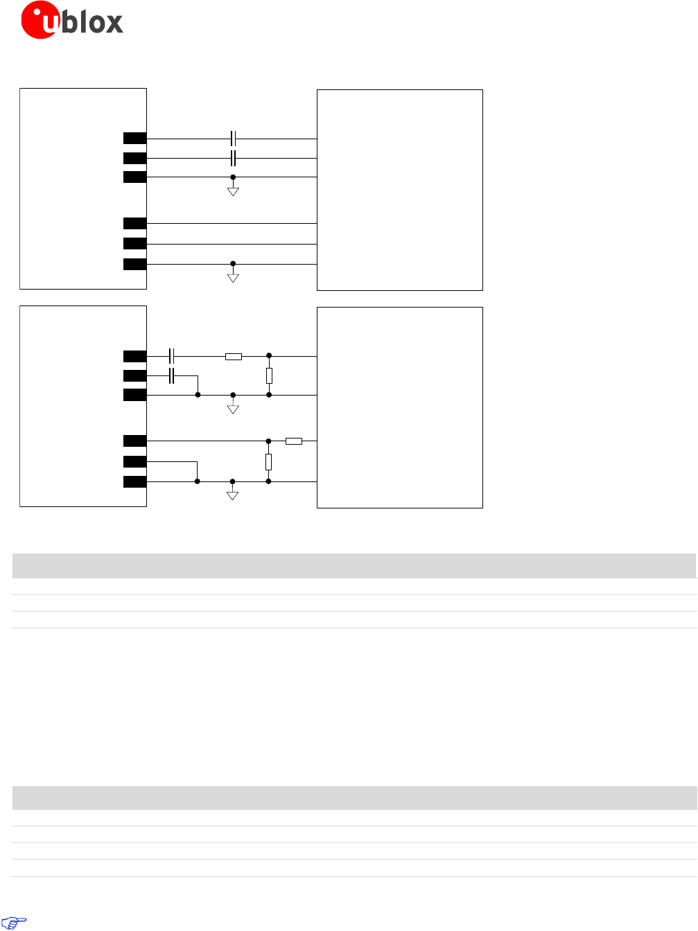
LISA-U1/LISA-H1 series - System Integration Manual
3G.G2-HW-10002-2 Advance Information System description
Page 70 of 116
LISA-U120/U130
C1
C2
54
SPK_N
53
SPK_P
GND
40
MIC_P
GND
Negative Analog IN
Positive Analog IN
Negative Analog OUT
Positive Analog OUT
Audio Device
Reference
Reference
39
MIC_N
LISA-U120/U130
54
SPK_N
53
SPK_P
GND
40
MIC_P
GND
Analog IN
Audio Device
Reference
Reference
39
MIC_N
Analog OUT
C3
C4 R2
R1
R4
R3
Figure 41: Application circuits to connect the module to audio devices with proper differential or single-ended input/output
Reference
Description
Part Number - Manufacturer
C1, C2, C3, C4
10 µF Capacitor X5R 0603 5% 6.3 V
GRM188R60J106M - Murata
R1, R3
0 Ω Resistor 0402 5% 0.1 W
RC0402JR-070RL - Yageo Phycomp
R2, R4
Not populated
Table 30: Connection to an Audio Device
1.11.2 Digital Audio interface
LISA-U120 and LISA-U130 modules support a bidirectional 4-wire I2S digital audio interface. The module acts as
master only. The applicable pins are described in Table 31:
Name
Description
Remarks
I2S_WA
I2S word alignment
Module output (master)
I2S_TXD
I2S transmit data
Module output
I2S_CLK
I2S clock
Module output (master)
I2S_RXD
I2S receive data
Module input
Table 31: I2S interface pins
The I2S interface pins ESD rating is 1 kV (contact discharge). A higher protection level could be required
if the lines are externally accessible on the application board. A higher protection level can be achieved
mounting an ESD protection (e.g. EPCOS CA05P4S14THSG varistor array) on the lines connected to
these pins.

LISA-U1/LISA-H1 series - System Integration Manual
3G.G2-HW-10002-2 Advance Information System description
Page 71 of 116
If the I2S digital audio pins are not used, they can be left unconnected on the application board.
The I2S interface can be can be used in two modes:
PCM mode
Normal I2S mode
To select the I2S digital audio interface the AT+USPM command parameters must assume these values (for more
details please refer to u-blox AT Commands Manual [2]):
<main_uplink>: “I2S input line”
<main_downlink>: “I2S output line”
Parameters of digital path can be configured and saved as the normal analog paths, using appropriate path
parameter as described in the u-blox AT Commands Manual [2], +USGC, +UMGC, +USTN AT command. Analog
gain parameters of microphone and speakers are unused when digital path is selected.
I2S_TX and I2S_RX are respectively parallel to the analog front end, so resources available for analog path can
be shared:
Digital filters and digital gains are available in both uplink and downlink direction. Configure using AT
commands
Ringer tone and service tone are mixed on the TX path when active (downlink)
The HF algorithm acts on I2S path
Refer to the u-blox AT Commands Manual [2]: AT+UI2S command for possible combinations of
connection and settings.
1.11.2.1 I2S interface - PCM mode
Main features of the I2S interface in PCM mode:
I2S runs in PCM - short alignment mode (configurable by AT commands)
Module functions as I2S master (I2S_CLK and I2S_WA signals generated by the module)
I2S_WA signal always runs at 8 kHz
I2S_WA toggles high for 1 or 2 CLK cycles of synchronization (configurable), then toggles low for 16 CLK
cycles of sample width. Frame length can be 1 + 16 = 17 bits or 2 + 16 = 18 bits
I2S_CLK frequency depends on frame length. Can be 17 x 8 kHz = 136 kHz or 18 x 8 kHz = 144 kHz
I2S_TX, I2S_RX data are 16 bit words with 8 kHz sampling rate, mono. Data is in 2’s complement notation.
MSB is transmitted first
When I2S_WA toggles high, the first synchronization bit is always low. Second synchronization bit (present
only in case of 2 bit long I2S_WA configuration) is MSB of the transmitted word (MSB is transmitted twice
in this case)
I2S_TX changes on I2S_CLK rising edge, I2S_RX changes on I2S_CLK falling edge
1.11.2.2 I2S interface - Normal I2S mode
Normal I2S supports:
16 bits word
Mono interface
8 kHz frequency
Main features of I2S interface in normal I2S mode:

LISA-U1/LISA-H1 series - System Integration Manual
3G.G2-HW-10002-2 Advance Information System description
Page 72 of 116
I2S_WA signal always runs at 8 kHz and synchronizes 2 channels (timeslots on WA high, WA low)
I2S_TX data are composed of 16 bit words, dual mono (the words are written on both channels). Data are
in 2’s complement notation. MSB is transmitted first. The bits are written on I2S_CLK rising or falling edge
(configurable)
I2S_RX data are read as 16 bit words, mono (words are read only on the timeslot with WA high). Data is
read in 2’s complement notation. MSB is read first. The bits are read on the I2S_CLK edge opposite to
I2S_TX writing edge (configurable)
I2S_CLK frequency is 16 bits x 2 channels x 8 kHz = 256 kHz
The modes are configurable through a specific AT command (refer to the related chapter in u-blox AT
Commands Manual [2], +UI2S AT command) and the following parameters can be set:
MSB can be 1 bit delayed or non-delayed on I2S_WA edge
I2S_TX data can change on rising or falling edge of I2S_CLK signal (rising edge in this example)
I2S_RX data are read on the opposite front of I2S_CLK signal
1.11.3 Voiceband processing system
The voiceband processing on the LISA-U120 and LISA-U130 modules is implemented in the DSP core inside the
baseband chipset. The analog audio front-end of the chipset is connected to the digital system through 16 bit
ADC converters in the uplink path, and through 16 bit DAC converters in the downlink path. External digital
audio devices can be interfaced directly to the DSP digital processing part via the I2S digital interface. The analog
amplifiers are skipped in this case.
Possible processing of audio signal are:
Speech encoding (uplink) and decoding (downlink).The following speech codecs are supported in firmware
on the DSP:
Fullrate, enhanced full rate, and half rate speech encoding and decoding
Adaptive multi rate (full rate and half rate) speech encoding and decoding
Mandatory sub-functions:
Discontinuous transmission, DTX (GSM 46.031, 46.041, 46.081 and 46.093 standards)
Voice activity detection, VAD (GSM 46.032, 46.042, 46.082 and 46.094 standards)
Background noise calculation (GSM 46.012, 46.022, 46.062 and 46.092 standards)
Function configurable via specific AT commands (refer to the u-blox AT Commands Manual [2])
Signal routing: +USPM command
Analog amplification, Digital amplification: +USGC,+CLVL, +CRSL, +CMUT command
Digital filtering: +UUBF, +UDBF commands
Hands-free algorithms (echo cancellation, Noise suppression, Automatic Gain control) +UHFP command
Sidetone generation (feedback of uplink speech signal to downlink path): +USTN command
Playing/mixing of alert tones:
Service tones: Tone generator with 3 sinus tones +UPAR command
User generated tones: Tone generator with 3 sinus tones +UTGN command
Midi melodies (for ringer): Synthesizer with up to 64 voices and a 48 kHz sampling rate, +UPAR
command
AMR files (for prompting): The storage format of AMR encoded audio content is defined in RFC3267
chapter 5 [9], +UPLAYFILE command
With exception of the speech encoder/decoder, this audio processing can be controlled by AT commands.
This processing is implemented within three different blocks of the voiceband processing system:
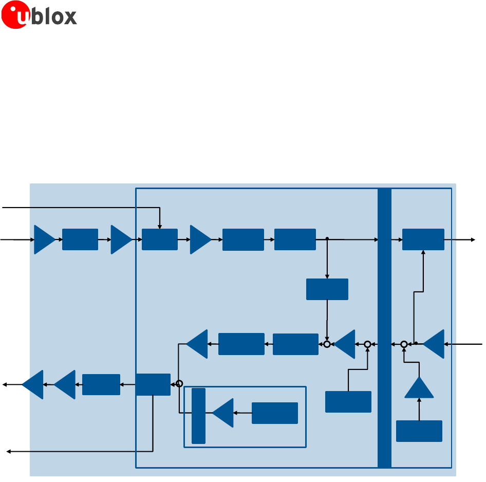
LISA-U1/LISA-H1 series - System Integration Manual
3G.G2-HW-10002-2 Advance Information System description
Page 73 of 116
Sample-based Voice-band Processing (single sample processed at 8 kHz, every 125 µs)
Frame-based Voice-band Processing (frames of 160 samples are processed every 20 ms)
MIDI synthesizer running at 47.6 kHz
These three blocks are connected by buffers (circular buffer and voiceband sample buffer) and sample rate
converters (for 8 to 47.6 kHz conversion) as illustrated in the block diagram in Figure 42, which summarizes the
voiceband audio processing in the DSP.
DAC
ADC
I2S_RXD
Switch
MIC
Microphone
Analog Gain
Uplink
filter 2
Uplink
filter 1
Hands-
free
To Radio
TX
Scal_Mic
Digital Gain
Sidetone
Downlink
filter 1
Downlink
filter 2
MIDI
player
SPK_P/N
Switch
I2S_TXD
Scal_Rec
Digital Gain
Mix_AFE
Digital Gain
SPK
Analog_gain
Gain_out
Digital Gain
Tone
Generator
From
Radio RX
Speech
level
I2Sx RX Sample Based Processing Frame Based
Processing
AMR
Player
Circular buffer
Voiceband Sample Buffer
18
dB
Power
Amplifier
Figure 42: Voiceband processing system block diagram

LISA-U1/LISA-H1 series - System Integration Manual
3G.G2-HW-10002-2 Advance Information System description
Page 74 of 116
1.12 General Purpose Input/Output (GPIO)
The LISA-U1/LISA-H1 series modules provide 5 pins (GPIO1, GPIO2, GPIO3, GPIO4 and GPIO5) which can be
configured as general purpose input or output, or can be configured to provide special functions via u-blox AT
commands (for further details refer to u-blox AT Commands Manual [2], +UGPIOC, +UGPIOR, +UGPIOW,
+UGPS, +UGPRF).
The available functions are described below:
GSM Tx burst indication: the GPIO1 can be configured by AT+UGPIOC to indicate when a GSM Tx
burst/slot occurs. The pin can be connected on the application board to an input pin of an application
processor to indicate when a GSM Tx burst/slot occurs
GPS supply enable: the GPIO2 is by default configured to enable or disable the supply of the u-blox GPS
receiver connected to the LISA-U1/LISA-H1 series module. The pin must be connected to the active-high
enable pin (or the active-low shutdown pin) of the voltage regulator that supplies the u-blox GPS receiver on
the application board. The pin is automatically set output high to switch on the u-blox GPS receiver when
the parameter <mode> of +UGPS AT command is set to 1, and otherwise it is set in tri-state with an internal
active pull-down enabled. The GPIO1, GPIO3, GPIO4 or GPIO5 can be configured by AT+UGPIOC to
provide this feature, alternatively to the default GPIO2
GPS data ready: the GPIO3 is by default configured to sense when the u-blox GPS receiver connected to
the LISA-U1/LISA-H1 series module is ready to send data by the DDC (I2C) interface. The pin must be
connected to the data ready output of the u-blox GPS receiver (i.e. the pin TxD1 of the u-blox GPS module)
on the application board. The pin automatically senses the line status to wake up the LISA-U1/LISA-H1 series
module from idle mode if the u-blox GPS receiver is ready to send data by the DDC (I2C) interface, when the
parameter <mode> of +UGPS AT command is set to 1, and otherwise it is set in tri-state with an internal
active pull-down enabled
GPS aiding synch: the GPIO4 is by default configured to provide a synchronization timing signal to the
u-blox GPS receiver connected to the LISA-U1/LISA-H1 series module. The pin must be connected to the
synchronization timing input of the u-blox GPS receiver (i.e. the pin EXTINT0 of the u-blox GPS module) on
the application board. The pin automatically provides a synchronization timing signal to the u-blox GPS
receiver when the parameter <mode> of +UGPS AT command is set to 1, and otherwise it is set in tri-state
with an internal active pull-down enabled
SIM card detection: the GPIO5 is by default configured to detect SIM card presence. The pin must be
connected on the application board to the SW2 pin of the SIM card connector with a 470 kΩ pull-down
resistor and SW1 pin of the SIM card connector must be pulled up to the module V_INT by a 1 kΩ pull-up
resistor
Network status indication: each GPIO (GPIO1, GPIO2, GPIO3, GPIO4 or GPIO5) can be configured by
AT+UGPIOC to indicate network status (registered home network, registered roaming, data transmission, no
service). The pin configured to provide this feature can be connected on the application board to an input
pin of an application processor or can drive a LED by a transistor with integrated resistors to indicate
network status
General purpose input: all the GPIOs (GPIO1, GPIO2, GPIO3, GPIO4 and GPIO5) can be configured by
AT+UGPIOC as input, sensing high or low digital level by AT+UGPIOR
General purpose output: all the GPIOs (GPIO1, GPIO2, GPIO3, GPIO4 and GPIO5) can be configured by
AT+UGPIOC as output, set in the high or low digital level by AT+UGPIOW, sensing high or low digital level
by AT+UGPIOR
Pad disabled: all the GPIOs (GPIO1, GPIO2, GPIO3, GPIO4 and GPIO5) can be configured by AT+UGPIOC
in tri-state, with an internal active pull-down enabled
LISA-U1/LISA-H1 series - System Integration Manual
3G.G2-HW-10002-2 Advance Information System description
Page 75 of 116
Name
Description
Remarks
GPIO1
GPIO
By default, any function is disabled and the internal active pull-down is enabled.
Can be alternatively configured by the AT+UGPIOC command
to provide the Output function
to provide the Input function
to provide the Network Status Indication function
to provide the GPS Supply Enable function
to provide the GSM Tx Burst Indication function
GPIO2
GPIO
By default, the pin is configured to provide the GPS Supply Enable function.
Can be alternatively configured by the AT+UGPIOC command
to provide the Output function
to provide the Input function
to provide the Network Status Indication function
to disable any function and enable the internal active pull-down
GPIO3
GPIO
By default, the pin is configured to provide the GPS Data Ready function.
Can be alternatively configured by the AT+UGPIOC command
to provide the Output function
to provide the Input function
to provide the Network Status Indication function
to provide the GPS Supply Enable function
to disable any function and enable the internal active pull-down
GPIO4
GPIO
By default, the pin is configured to provide the GPS Aiding Synch function.
Can be alternatively configured by the AT+UGPIOC command
to provide the Output function
to provide the Input function
to provide the Network Status Indication function
to provide the GPS Supply Enable function
to disable any function and enable the internal active pull-down
GPIO5
GPIO
By default, the pin is configured to provide the SIM card detection function.
Can be alternatively configured by the AT+UGPIOC command
to provide the Output function
to provide the Input function
to provide the Network Status Indication function
to provide the GPS Supply Enable function
to disable any function and enable the internal active pull-down
Table 32: GPIO pins
The GPIO pins ESD rating is 1 kV (contact discharge). A higher protection level could be required if the
lines are externally accessible on the application board. A higher protection level can be achieved
mounting an ESD protection (e.g. EPCOS CA05P4S14THSG varistor array) on the lines connected to
these pins.
An application circuit for a typical GPIO usage (GPS supply enable, GPS aiding synch, GPS data ready, SIM card
detection, Network indication) is described in Figure 43.
Use transistors with at least an integrated resistor in the base pin or otherwise put a 10 kΩ resistor on
the board in series to the GPIO.
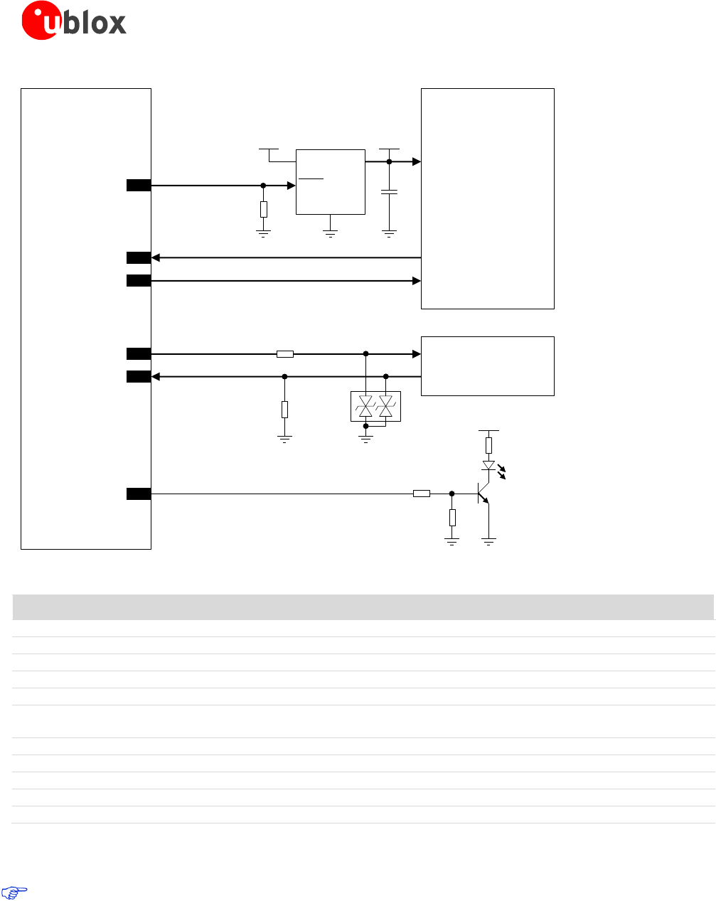
LISA-U1/LISA-H1 series - System Integration Manual
3G.G2-HW-10002-2 Advance Information System description
Page 76 of 116
SIM card holder
SW1
SW2
4
V_INT
51
GPIO5
R3
R2
OUTIN
GND
LDO Regulator
SHDN
3V8 1V8
GPIO3
GPIO4
TxD1
EXTINT0
23
24
R1
VCC
GPIO2 21
LISA-U1/LISA-H1
series
u-blox
1.8 V GPS receiver
U1
J1
C1
R4
R6
3V8
Network Indicator
R5
GPS Supply Enable
GPS Data Ready
GPS Aiding Synch
SIM Detection
20
GPIO1
DL1
T1
D1
Figure 43: GPIO application circuit
Reference
Description
Part Number - Manufacturer
R1
4.7 kΩ Resistor 0402 5% 0.1 W
Various manufacturers
U1
Voltage Regulator for GPS Receiver
See GPS Module Hardware Integration Manual
R2
1 kΩ Resistor 0402 5% 0.1 W
Various manufacturers
R3
470 kΩ Resistor 0402 5% 0.1 W
Various manufacturers
D1
ESD Transient Voltage Suppressor
USB0002RP or USB0002DP - AVX
J1
SIM Card Holder
Various Manufacturers,
CCM03-3013LFT R102 - C&K Components
R4
10 kΩ Resistor 0402 5% 0.1 W
Various manufacturers
R5
47 kΩ Resistor 0402 5% 0.1 W
Various manufacturers
R6
820 Ω Resistor 0402 5% 0.1 W
Various manufacturers
DL1
LED Red SMT 0603
LTST-C190KRKT - Lite-on Technology Corporation
T1
NPN BJT Transistor
BC847 - Infineon
Table 33: Components for GPIO application circuit
If the GPIO pins are not used, they can be left unconnected on the application board.
LISA-U1/LISA-H1 series - System Integration Manual
3G.G2-HW-10002-2 Advance Information System description
Page 77 of 116
1.13 Reserved pins (RSVD)
LISA-U1/LISA-H1 series modules have some pins reserved for future use. All the RSVD pins, except pin number 5,
can be left unconnected on the application board. The application circuit is illustrated in Figure 44.
Pin 5 (RSVD) must be connected to GND.
LISA-U120/U130
5
RSVD
52
RSVD
74
RSVD
LISA-U100/U110
LISA-H100/H110
5
RSVD
52
RSVD
74
RSVD
39
RSVD
40
RSVD
41
RSVD
42
RSVD
43
RSVD
44
RSVD
53
RSVD
53
RSVD
Figure 44: Application circuit for the reserved pins (RSVD)
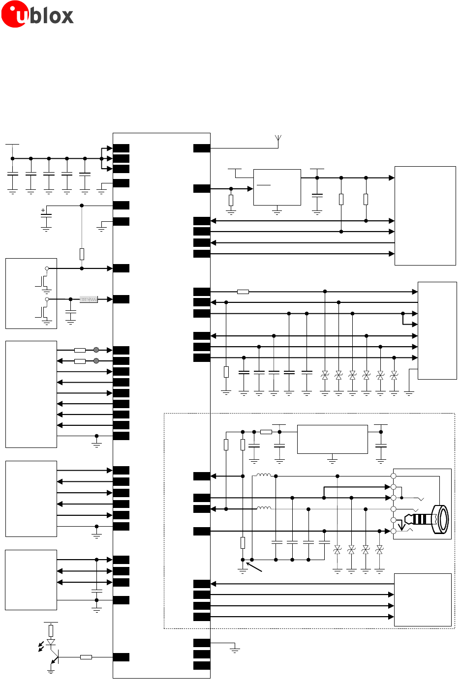
LISA-U1/LISA-H1 series - System Integration Manual
3G.G2-HW-10002-2 Advance Information System description
Page 78 of 116
1.14 Schematic for LISA-U1/LISA-H1 series module integration
Figure 45 is an example of a schematic diagram where a LISA-U1/LISA-H1 series module is integrated into an
application board, using all the interfaces of the module.
47pF
SIM Card Holder
CCVCC (C1)
CCVPP (C6)
CCIO (C7)
CCCLK (C3)
CCRST (C2)
GND (C5)
47pF 47pF 100nF
50VSIM
48SIM_IO
47SIM_CLK
49SIM_RST
47pF
SW1
SW2
4V_INT
51GPIO5
470k
1k
ESD ESD ESD ESD ESD ESD
TXD
RXD
RTS
CTS
DTR
DSR
RI
DCD
GND
15 TXD
12 DTR
16 RXD
13 RTS
14 CTS
9DSR
10 RI
11 DCD
GND
3V8
330µF 39pF GND
10nF100nF 10pF
LISA-U1/LISA-H1 series
62 VCC
63 VCC
61 VCC
+
100µF
2V_BCKP
MOSI
MISO
SCLK
Interrupt
GPIO
GND
56 SPI_MOSI
59 SPI_MRDY
57 SPI_MISO
55 SPI_SCLK
58 SPI_SRDY
GND
VBUS
D+
D-
GND
18 VUSB_DET
27 USB_D+
26 USB_D-
GND
100nF
5RSVD
52RSVD
74RSVD
GND
RTC
back-up
27pF 27pF 27pF
82nH
54SPK_N
53SPK_P
39
MIC_N
40MIC_P
ESD
Headset Connector
ESD
INOUT
GND
Low Noise LDO Regulator 3V8
2.2k
2.2k
10µF
2.2k
2.2k 10µF
2V5
Sense lines connected
to GND in one star point
82nH
27pF
10µF
ESD ESD
u-blox
1.8V GPS Receiver
4.7k
OUTIN
GND
LDO Regulator
SHDN
SDA
SCL
4.7k
3V8 1V8_GPS
SDA2
SCL2
GPIO3
GPIO4
TxD1
EXTINT0
46
45
23
24
4.7k
VCC
GPIO2 21
ANT 68 Antenna
1.8V DTE
1.8V SPI Master
USB 2.0 Host
1.8V Digital
Audio Device
I2S_RXD
I2S_CLK
I2S_TXD
I2S_CLK
I2S_TXD
I2S_WA
I2S_RXD
I2S_WA
44
43
42
41
LISA-U120/U130 only
20 GPIO1
3V8
Network
Indicator
22 RESET_N
Ferrite Bead
47pF
Application
Processor
Open
Drain
Output
19 PWR_ON
100kΩ
Open
Drain
Output
0Ω
0Ω
TP
TP
Figure 45: Example of schematic diagram to integrate LISA module in an application board, using all the interfaces

LISA-U1/LISA-H1 series - System Integration Manual
3G.G2-HW-10002-2 Advance Information System description
Page 81 of 116
IMPORTANT: Manufacturers of portable applications incorporating the LISA-U1/LISA-H1 series
modules are required to have their final product certified and apply for their own FCC Grant
and Industry Canada Certificate related to the specific portable device. This is mandatory to
meet the SAR requirements for portable devices.
Changes or modifications not expressly approved by the party responsible for compliance
could void the user's authority to operate the equipment.

LISA-U1/LISA-H1 series - System Integration Manual
3G.G2-HW-10002-2 Advance Information Design-In
Page 82 of 116
2 Design-In
2.1 Design-in checklist
This section provides a design-in checklist.
2.1.1 Schematic checklist
The following are the most important points for a simple schematic check:
DC supply must provide a nominal voltage at VCC pin above the minimum operating range limit.
DC supply must be capable of providing 2.5 A current pulses, providing a voltage at VCC pin above the
minimum operating range limit and with a maximum 400 mV voltage drop from the nominal value.
VCC supply should be clean, with very low ripple/noise: suggested passive filtering parts can be inserted.
VCC voltage must ramp from 2.5 V to 3.2 V within 1 ms to allow a proper switch-on of the module.
Connect only one DC supply to VCC: different DC supply systems are mutually exclusive.
Do not leave PWR_ON floating: add a pull-up resistor to V_BCKP.
Don’t apply loads which might exceed the limit for maximum available current from V_INT supply.
Check that voltage level of any connected pin does not exceed the relative operating range.
Capacitance and series resistance must be limited on each SIM signal to match the SIM specifications.
Insert the suggested low capacitance ESD protection and passive filtering parts on each SIM signal.
Check UART signals direction, since the signal names follow the ITU-T V.24 Recommendation [3].
Provide appropriate access to USB interface and/or to UART RxD, TxD lines and access to PWR_ON
and/or RESET_N lines on the application board in order to flash/upgrade the module firmware.
Provide appropriate access to USB interface and/or to UART RxD, TxD, CTS, RTS lines for debugging.
Add a proper pull-up resistor to a proper supply on each DDC (I2C) interface line, if the interface is used.
Capacitance and series resistance must be limited on each line of the DDC interface.
Use transistors with at least an integrated resistor in the base pin or otherwise put a 10 kΩ resistor on
the board in series to the GPIO when those are used to drive LEDs.
Connect the pin number 5 (RSVD) to ground.
Insert the suggested passive filtering parts on each used analog audio line.
Check the digital audio interface specifications to connect a proper device.
Provide proper precautions for ESD immunity as required on the application board.
All unused pins can be left floating on the application board except the PWR_ON pin (must be
connected to V_BCKP by a pull-up resistor) and the RSVD pin number 5 (must be connected to GND).
2.1.2 Layout checklist
The following are the most important points for a simple layout check:
Check 50 nominal characteristic impedance of the RF transmission line connected to ANT pad.
Follow the recommendations of the antenna producer for correct antenna installation and deployment
(PCB layout and matching circuitry).
Ensure no coupling occurs with other noisy or sensitive signals (primarily MIC signals, audio output
signals, SIM signals).
VCC line should be wide and short.
Route VCC supply line away from sensitive analog signals.

LISA-U1/LISA-H1 series - System Integration Manual
3G.G2-HW-10002-2 Advance Information Design-In
Page 83 of 116
The high-power audio outputs lines on the application board must be wide enough to minimize series
resistance.
Ensure proper grounding.
Consider “No-routing” areas for the Data Module footprint.
Optimize placement for minimum length of RF line and closer path from DC source for VCC.
Design USB_D+ / USB_D- connection as 90 differential pair.
Keep routing short and minimize parasitic capacitance on the SPI lines to preserve signal integrity.
2.1.3 Antenna checklist
Antenna should have 50 impedance, V.S.W.R less then 3:1, recommended 2:1 on operating bands in
deployment geographical area.
Follow the recommendations of the antenna producer for correct antenna installation and deployment
(PCB layout and matching circuitry).
Antenna should have built in DC resistor to ground to get proper Antenna detection functionality.
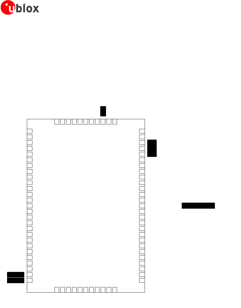
LISA-U1/LISA-H1 series - System Integration Manual
3G.G2-HW-10002-2 Advance Information Design-In
Page 84 of 116
2.2 Design Guidelines for Layout
The following design guidelines must be met for optimal integration of LISA-U1/LISA-H1 series modules on the
final application board.
2.2.1 Layout guidelines per pin function
This section groups LISA-U1/LISA-H1 series modules pins by signal function and provides a ranking of importance
in layout design.
Very Important
Careful Layout
Common Practice
Legend:
V_BCKP
GND
V_INT
RSVD
GND
GND
GND
DSR
RI
DCD
DTR
GND
RTS
CTS
TXD
RXD
GND
VUSB_DET
PWR_ON
GPIO1
GPIO2
RESET_N
GPIO3
GPIO4
GND
USB_D-
USB_D+
2
3
4
5
6
7
8
9
10
11
12
1
13
14
15
16
17
18
19
20
21
22
23
24
25
26
27
GND
VCC
VCC
VCC
GND
SPI_MRDY
SPI_SRDY
SPI_MISO
SPI_MOSI
SPI_SCLK
SPK_N
GND
SPK_P
RSVD
GPIO5
VSIM
SIM_RST
SIM_IO
SIM_CLK
SDA
SCL
I2S_RXD
I2S_CLK
I2S_TXD
I2S_WA
MIC_P
MIC_N
64
63
62
61
60
59
58
57
56
55
54
65
53
52
51
50
49
48
47
46
45
44
43
42
41
40
39
29
30
31
32
33
34
35
36
37
38
28
GND
GND
GND
GND
GND
GND
GND
GND
GND
GND
GND
75
74
73
72
71
70
69
68
67
66
76
GND
RSVD
GND
GND
GND
GND
GND
ANT
GND
GND
GND
Figure 46: Module pin-out with ranked importance for layout design (LISA top view)

LISA-U1/LISA-H1 series - System Integration Manual
3G.G2-HW-10002-2 Advance Information Design-In
Page 85 of 116
Rank
Function
Pin(s)
Layout
Remarks
1st
RF Antenna In/out
Very Important
Design for 50 characteristic impedance.
See section 2.2.1.1
2nd
Main DC Supply
Very Important
VCC line should be wide and short. Route away
from sensitive analog signals.
See section 2.2.1.2
3rd
USB Signals
Very Important
Route USB_D+ and USB_D- as differential lines:
design for 90 differential impedance.
See section 2.2.1.3
4th
Analog Audio
Careful Layout
Avoid coupling with noisy signals.
See section 2.2.1.4
Audio Inputs
MIC_P, MIC_N
Audio Outputs
SPK_P, SPK_N
5th
Ground
GND
Careful Layout
Provide proper grounding.
See section 2.2.1.5
6th
Sensitive Pin :
Careful Layout
Avoid coupling with noisy signals.
See section 2.2.1.6
Backup Voltage
V_BCKP
Power On
PWR_ON
7th
High-speed digital pins:
Careful Layout
Avoid coupling with sensitive signals.
See section 2.2.1.7
SPI Signals
SPI_SCLK, SPI_MISO,
SPI_MOSI, SPI_SRDY,
SPI_MRDY
8th
Digital pins and
supplies:
Common
Practice
Follow common practice rules for digital pin
routing.
See section 2.2.1.8
SIM Card Interface
VSIM, SIM_CLK,
SIM_IO, SIM_RST
Digital Audio
(If implemented)
I2S_CLK, I2S_RXD,
I2S_TXD, I2S_WA
DDC
SCL, SDA
UART
TXD, RXD, CTS, RTS,
DSR, RI, DCD, DTR
External Reset
RESET_N
General Purpose I/O
GPIO1, GPIO2, GPIO3,
GPIO4, GPIO5
USB detection
VUSB_DET
Supply for Interfaces
V_INT
Table 34: Pin list in order of decreasing importance for layout design
2.2.1.1 RF antenna connection
The RF antenna connection pin ANT is very critical in layout design. The PCB line must be designed to provide
50 nominal characteristic impedance and minimum loss up to radiating element.
Provide proper transition between the ANT pad to application board PCB
Increase GND keep-out (i.e. clearance) for ANT pad to at least 250 µm up to adjacent pads metal definition
and up to 500 µm on the area below the Data Module, as described in Figure 47.
Add GND keep-out (i.e. clearance) on buried metal layers below ANT pad and below any other pad of
component present on the RF line, if top-layer to buried layer dielectric thickness is below 200 µm, to reduce
parasitic capacitance to ground (see Figure 47 for the description keep-out area below ANT pad)
The transmission line up to antenna connector or pad may be a micro strip or a stripline. In any case must be
designed to achieve 50 Ω characteristic impedance
Microstrip lines are usually easier to implement and the reduced number of layer transitions up to antenna
connector simplifies the design and diminishes reflection losses. However, the electromagnetic field extends
to the free air interface above the stripline and may interact with other circuitry
USB_D-
USB_D+
VCC
ANT
LISA-U1/LISA-H1 series - System Integration Manual
3G.G2-HW-10002-2 Advance Information Design-In
Page 86 of 116
Buried striplines exhibit better shielding to external and internally generated interferences. They are therefore
preferred for sensitive application. In case a stripline is implemented, carefully check that the via pad-stack
does not couple with other signals on the crossed and adjacent layers
Minimize the transmission line length; the insertion loss should be minimized as much as possible, in the
order of a few tenths of a dB
The transmission line should not have abrupt change to thickness and spacing to GND, but must be uniform
and routed as smoothly as possible
The transmission line must be routed in a section of the PCB where minimal interference from noise sources
can be expected
Route RF transmission line far from other sensitive circuits as it is a source of electromagnetic interference
Avoid coupling with VCC routing and analog audio lines
Ensure solid metal connection of the adjacent metal layer on the PCB stack-up to main ground layer
Add GND vias around transmission line
Ensure no other signals are routed parallel to transmission line, or that other signals cross on adjacent metal
layer
If the distance between the transmission line and the adjacent GND area (on the same layer) does not
exceed 5 times the track width of the micro strip, use the “Coplanar Waveguide” model for 50 Ω
characteristic impedance calculation
Don’t route microstrip line below discrete component or other mechanics placed on top layer
When terminating transmission line on antenna connector (or antenna pad) it is very important to strictly
follow the connector manufacturer’s recommended layout
GND layer under RF connectors and close to buried vias should be cut out in order to remove stray
capacitance and thus keep the RF line 50 Ω. In most cases the large active pad of the integrated antenna or
antenna connector needs to have a GND keep-out (i.e. clearance) at least on first inner layer to reduce
parasitic capacitance to ground. Note that the layout recommendation is not always available from
connector manufacturer: e.g. the classical SMA Pin-Through-Hole needs to have GND cleared on all the
layers around the central pin up to annular pads of the four GND posts. Check 50 Ω impedance of ANT line
Ensure no coupling occurs with other noisy or sensitive signals
Min. 500 um
Min.
250 um
Top layer Buried metal layer
GND
plane
Microstrip
50 ohm
Figure 47: GND keep-out area on the top layer around the ANT pad and on the buried metal layer below the ANT pad
Any RF transmission line on PCB should be designed for 50 Ω characteristic impedance.
Ensure no coupling occurs with other noisy or sensitive signals.
LISA-U1/LISA-H1 series - System Integration Manual
3G.G2-HW-10002-2 Advance Information Design-In
Page 87 of 116
Additional guidelines for products marked with the FCC logo - United States only
LISA-U1/LISA-H1 series modules can only be used with a host antenna circuit trace layout according to below
guidelines and a host system designer must follow the guidelines to keep the original Grant of LISA-U1/LISA-H1
series modules.
Strict compliance to the layout reference design already approved (described in the following guidelines)
is required to ensure that only approved antenna shall be used in the host system.
If in a host system there is any difference from the trace layout already approved, it requires a Class II
permissive change or a new grant as appropriate as FCC defines.
Compliance of this device in all final host configurations is the responsibility of the Grantee.
The approved reference design for LISA-U1/LISA-H1 series modules has a structure of four layers described in the
following.
The Layer 1 (top layer, see Figure 48) provides a micro strip line to connect the ANT pin of the LISA-U1/LISA-H1
series module to the antenna connector. The ANT pin of the LISA-U1/LISA-H1 series module has to be soldered
on the designed pad which is connected to the antenna connector by a micro strip. The characteristics of the
micro strip line (coplanar wave guide) are the following:
Thickness = 0.035 mm
Width = 0.26 mm
Length = 7.85 mm
Gap (signal to GND) = 0.5 mm
The micro strip line must be designed to achieve 50 Ω characteristic impedance: the dimensions of the micro
strip line have to be calculated in a host system according to PCB characteristics provided by PCB manufacturer.
Pad designed for the ANT pin
Antenna connector
Microstrip line
Figure 48: Layer 1 (top layer) of u-blox approved interface board for LISA-U1/LISA-H1 series modules
The thickness of the dielectric (FR4 Prepreg 1080) from Layer 1 (top layer) to Layer 2 (inner layer) is 0.27 mm.
The Layer 2 (inner layer, described in Figure 49) provides a GND plane.
Layer 2 thickness is 0.035 mm.
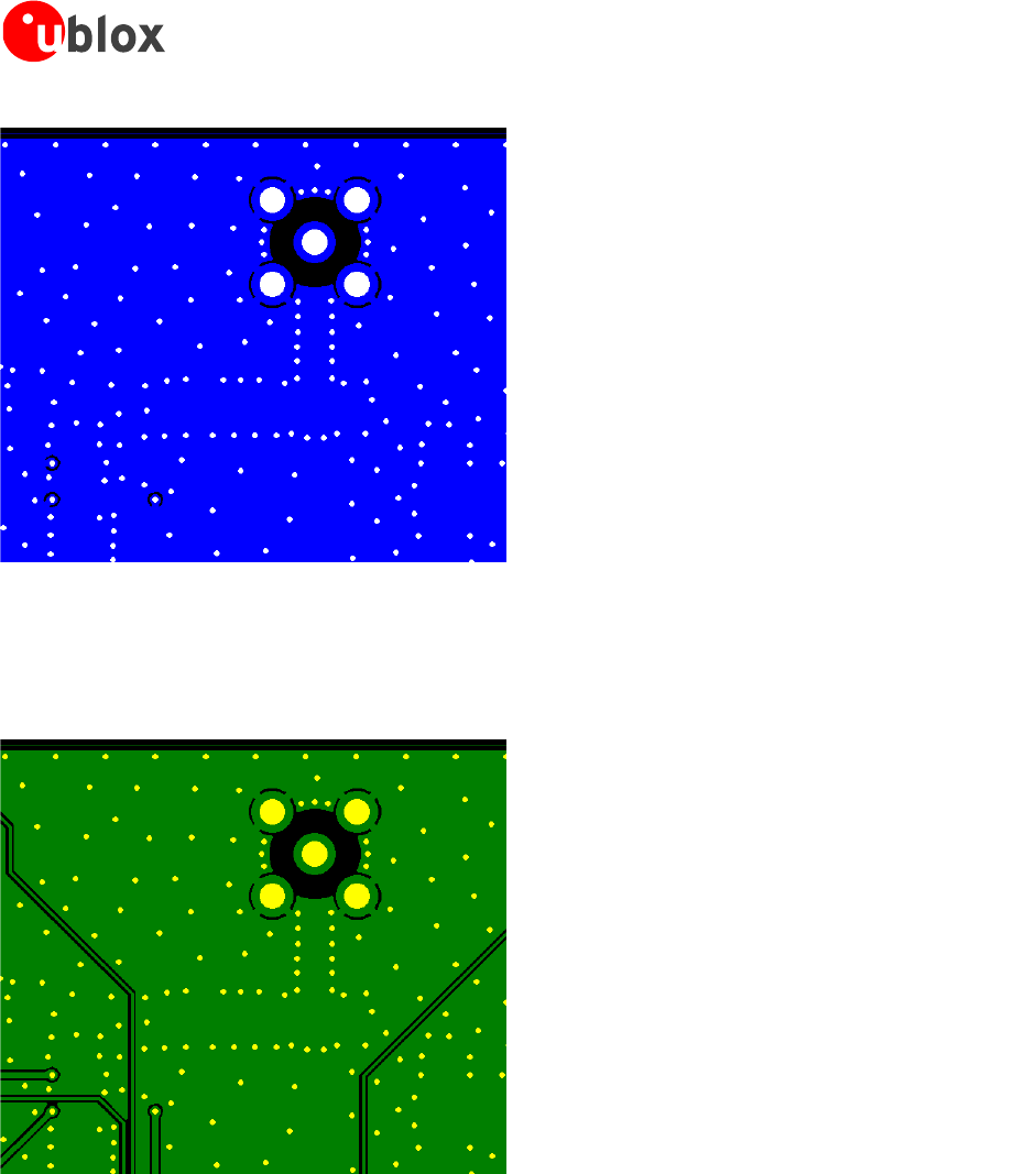
LISA-U1/LISA-H1 series - System Integration Manual
3G.G2-HW-10002-2 Advance Information Design-In
Page 88 of 116
Figure 49: Layer 2 (inner layer) of u-blox approved interface board for LISA-U1/LISA-H1 series modules
The thickness of the dielectric (FR4 Laminate 7628) from Layer 2 (inner layer) to Layer 3 (inner layer) is 0.76 mm.
The Layer 3 (inner layer, described in Figure 50) is designed for signals routing and GND plane.
Layer 3 thickness is 0.035 mm.
Figure 50: Layer 3 (inner layer) of u-blox approved interface board for LISA-U1/LISA-H1 series modules
The thickness of the dielectric (FR4 Prepreg 1080) from Layer 3 (inner layer) to Layer 4 (bottom layer) is 0.27 mm.
The Layer 4 (bottom layer, described in Figure 51) is designed for signals routing, components placement and
GND plane.
Layer 4 thickness is 0.035 mm.
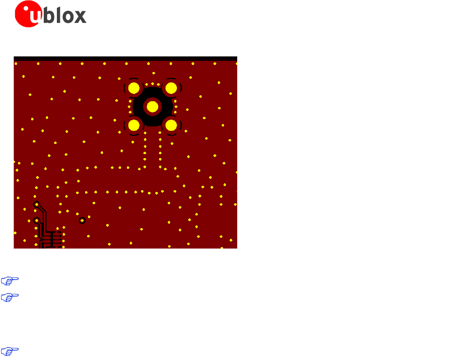
LISA-U1/LISA-H1 series - System Integration Manual
3G.G2-HW-10002-2 Advance Information Design-In
Page 89 of 116
Figure 51: Layer 4 (bottom layer) of u-blox approved interface board for LISA-U1/LISA-H1 series modules
The antenna must not exceed 3dBi gain to preserve the original u-blox FCC ID.
The antenna must be installed and operated with a minimum distance of 20 cm from all persons and
must not be co-located or operating in conjunction with any other antenna or transmitter.
Under the requirements of FCC Section 15.212(a)-iv, the module must contain a permanently attached antenna,
or contain a unique antenna connector, and be marketed and operated only with specific antenna(s).
In accordance with FCC Section 15.203, the antenna should use a unique coupling connector to the
approved reference design for LISA-U1/LISA-H1 series modules, in order to ensure that the design will
not be deployed with antenna of different characteristic from the approved type.
The use of standard SMA type connector is not permitted, as its standard usage allows easy replacement of the
attached antenna. However RP-SMA (Reverse-Polarized-SMA) connector type fulfills the minimum requirements
to prevent exchangeability of antenna on the reference design.
2.2.1.2 Main DC supply connection
The DC supply of LISA-U1/LISA-H1 series modules is very important for the overall performance and functionality
of the integrated product. For detailed description, check the design guidelines in section 1.5.2. Some main
characteristics are:
VCC pins are internally connected, but it is recommended to use all the available pins in order to minimize
the power loss due to series resistance
VCC connection may carry a maximum burst current in the order of 2.5 A. Therefore, it is typically
implemented as a wide PCB line with short routing from DC supply (DC-DC regulator, battery pack, etc)
The module automatically initiates an emergency shutdown if supply voltage drops below hardware
threshold. In addition, reduced supply voltage can set a worst case operation point for RF circuitry that may
behave incorrectly. It follows that each voltage drop in the DC supply track will restrict the operating margin
at the main DC source output. Therefore, the PCB connection must exhibit a minimum or zero voltage drop.
Avoid any series component with Equivalent Series Resistance (ESR) greater than a few milliohms
Given the large burst current, VCC line is a source of disturbance for other signals. Therefore route VCC
through a PCB area separated from sensitive analog signals. Typically it is good practice to interpose at least
one layer of PCB ground between VCC track and other signal routing
The VCC supply current supply flows back to main DC source through GND as ground current: provide
adequate return path with suitable uninterrupted ground plane to main DC source

LISA-U1/LISA-H1 series - System Integration Manual
3G.G2-HW-10002-2 Advance Information Design-In
Page 90 of 116
A tank capacitor with low ESR is often used to smooth current spikes. This is most effective when placed as
close as possible to VCC. From main DC source, first connect the capacitor and then VCC. If the main DC
source is a switching DC-DC converter, place the large capacitor close to the DC-DC output and minimize
the VCC track length. Otherwise consider using separate capacitors for DC-DC converter and LISA-U1/LISA-
H1 series module tank capacitor. Note that the capacitor voltage rating may be adequate to withstand the
charger over-voltage if battery-pack is used
VCC is directly connected to the RF power amplifiers. Add capacitor in the pF range from VCC to GND along
the supply path
Since VCC is directly connected to RF Power Amplifiers, voltage ripple at high frequency may result in
unwanted spurious modulation of transmitter RF signal. This is more likely to happen with switching DC-DC
converters, in which case it is better to select the highest operating frequency for the switcher and add a
large L-C filter before connecting to the LISA-U1/LISA-H1 series modules in the worst case
The large current generates a magnetic field that is not well isolated by PCB ground layers and which may
interact with other analog modules (e.g. VCO) even if placed on opposite side of PCB. In this case route VCC
away from other sensitive functional units
The typical GSM burst has a periodic nature of approx. 217 Hz, which lies in the audible audio range. Avoid
coupling between VCC and audio lines (especially microphone inputs)
If VCC is protected by transient voltage suppressor / reverse polarity protection diode to ensure that the
voltage maximum ratings are not exceeded, place the protecting device along the path from the DC source
toward the LISA-U1/LISA-H1 series module, preferably closer to the DC source (otherwise functionality may
be compromised)
VCC line should be wide and short.
Route away from sensitive analog signals.
2.2.1.3 USB signal
The LISA-U1/LISA-H1 series modules include a high-speed USB 2.0 compliant interface with a maximum
throughput of 480 Mb/s (see Section 1.9.3). Signals USB_D+ / USB_D- carry the USB serial data and signaling.
The lines are used in single ended mode for relatively low speed signaling handshake, as well as in differential
mode for fast signaling and data transfer. Characteristic impedance of USB_D+ / USB_D- lines is specified by
USB standard. The most important parameter is the differential characteristic impedance applicable for odd-
mode electromagnetic field, which should be as close as possible to 90 differential: signal integrity may be
degraded if PCB layout is not optimal, especially when the USB signaling lines are very long.
Route USB_D+ / USB_D- lines as a differential pair
Ensure the differential characteristic impedance is as close as possible to 90
Consider design rules for USB_D+ / USB_D- similar to RF transmission lines, being them coupled differential
micro-strip or buried stripline: avoid any stubs, abrupt change of layout, and route on clear PCB area
2.2.1.4 Analog audio (LISA-U120 / LISA-U130 only)
Accurate analog audio design is very important to obtain clear and high quality audio. The GSM signal burst has
a repetition rate of 217 Hz that lies in the audible range. A careful layout is required to reduce the risk of noise
from audio lines due to both VCC burst noise coupling and RF detection.
Analog audio is separated in the two paths,
1. Audio Input (uplink path): MIC_P / MIC_N
2. Audio Outputs (downlink path): SPK_P / SPK_N
The most sensitive is the uplink path, since the analog input signals are in the microVolts range.

LISA-U1/LISA-H1 series - System Integration Manual
3G.G2-HW-10002-2 Advance Information Design-In
Page 91 of 116
Avoid coupling of any noisy signals to microphone input lines
It is strongly recommended to route MIC signals away from battery and RF antenna lines. Try to skip fast
switching digital lines as well
Keep ground separation from other noisy signals. Use an intermediate GND layer or vias wall for coplanar
signals
MIC_P and MIC_N are sensed differentially within the module. Therefore they should be routed as a
differential pair up to the audio signal source
Cross other signals lines on adjacent layers with 90° crossing
Place bypass capacitor for RF very close to active microphone. The preferred microphone should be designed
for GSM applications which typically have internal built-in bypass capacitor for RF very close to active device.
If the integrated FET detects the RF burst, the resulting DC level will be in the pass-band of the audio
circuitry and cannot be filtered by any other device
The bias for an external electret active microphone is not provided by the module. Verify that microphone is
properly biased from an external low noise supply and verify that the supply noise is properly filtered
Output audio lines have two separated configurations.
SPK_P / SPK_N are high level balanced output. They are DC coupled and must be used with a speaker
connected in bridge configuration
Route SPK_P / SPK_N as differential pair, to reduce differential noise pick-up. The balanced configuration
will help reject the common mode noise
Consider enlarging PCB lines, to reduce series resistive losses, when the audio output is directly connected to
low impedance speaker transducer
Use twisted pair cables for balanced audio usage
If DC decoupling is required, a large capacitor needs to be used, typically in the microFarad range,
depending on the load impedance, in order to not increase the lower cut-off frequency of its High-Pass RC
filter response
2.2.1.5 Module grounding
Good connection of the module with application board solid ground layer is required for correct RF
performance. It significantly reduces EMC issues and provides a thermal heat sink for the module.
Connect each GND pin with application board solid GND layer. It is strongly recommended that each GND
pad surrounding VCC pins have one or more dedicated via down to the application board solid ground layer
The shielding metal tabs are connected to GND, and are a fundamental part of electrical grounding and
thermal heat-sink. Connect them to board solid ground layer, by soldering them on the baseboard using
PCB plated through holes connected to GND net
If the application board is a multilayer PCB, then it is required to connect together each GND area with
complete via stack down to main board ground layer
It is recommended to implement one layer of the application board as ground plane
Good grounding of GND pads will also ensure thermal heat sink. This is critical during call connection, when
the real network commands the module to transmit at maximum power: proper grounding helps prevent
module overheating
2.2.1.6 Other sensitive pins
A few other pins on the LISA-U1/LISA-H1 series modules requires careful layout.
RTC supply (V_BCKP): avoid injecting noise on this voltage domain as it may affect the stability of sleep
oscillator

LISA-U1/LISA-H1 series - System Integration Manual
3G.G2-HW-10002-2 Advance Information Design-In
Page 92 of 116
Power On (PWR_ON): is the digital input to switch-on the LISA-U1/LISA-H1 series modules. Ensure that the
voltage level is well defined during operation and no transient noise is coupled on this line, otherwise the
module might detect a spurious power on request
2.2.1.7 High-speed digital pins
The Serial Peripheral Interface Bus (SPI) interface can be used for high speed data transfer (UMTS/HSPA) between
the LISA-U1/LISA-H1 series modules and the host processor, with a data rate up to 20 Mb/s (see Section 1.9.3).
The high-speed data rate is carried by signals SPI_SCLK, SPI_MISO and SPI_MOSI, while SPI_SRDY and
SPI_MRDY behave as handshake signals with relatively low activity.
High-speed signals become sources of digital noise, route away from RF and other sensitive analog signals
Keep routing short and minimize parasitic capacitance to preserve digital signal integrity
2.2.1.8 Digital pins and supplies
External Reset (RESET_N): input for external reset, a logic low voltage will reset the module
SIM Card Interface (VSIM, SIM_CLK, SIM_IO, SIM_RST): the SIM layout may be critical if the SIM card is
placed far away from the LISA-U1/LISA-H1 series modules or in close proximity to the RF antenna. In the first
case the long connection can cause the radiation of some harmonics of the digital data frequency. In the
second case the same harmonics can be picked up and create self-interference that can reduce the sensitivity
of GSM Receiver channels whose carrier frequency is coincidental with harmonic frequencies. The latter
case, placing the RF bypass capacitors, suggested in Figure 20, near the SIM connector will mitigate the
problem. In addition, since the SIM card is typically accessed by the end user, it can be subjected to ESD
discharges: add adequate ESD protection to protect module SIM pins near the SIM connector.
Digital Audio (I2S_CLK, I2S_RX, I2S_TX, I2S_WA): the I2S interface requires the same consideration
regarding electro-magnetic interference as the SIM card. Keep the traces short and avoid coupling with RF
line or sensitive analog inputs
DDC (SCL, SDA): the DDC interface requires the same consideration regarding electro-magnetic
interference as the SIM card. Keep the traces short and avoid coupling with RF line or sensitive analog inputs
UART (TXD, RXD, CTS, RTS, DSR, RI, DCD, DTR): the serial interface requires the same consideration
regarding electro-magnetic interference as the SIM card. Keep the traces short and avoid coupling with RF
line or sensitive analog inputs
General Purpose I/O (GPIOx): the general purpose input/output pins are generally not critical for layout
Reserved pins: these pins are reserved for future use. Leave them unconnected on the baseboard
USB detection (VUSB_DET): this input will generate an interrupt to the baseband processor for USB
detection. The USB supply (5.0 V typ.) must be provided to VUSB_DET by the connected USB host to enable
the USB interface of the module
Interfaces Supply (V_INT): this supply output is generated by an integrated switching step down converter,
used internally to supply the digital interfaces. Because of this, it can be a source of noise: avoid coupling
with sensitive signals
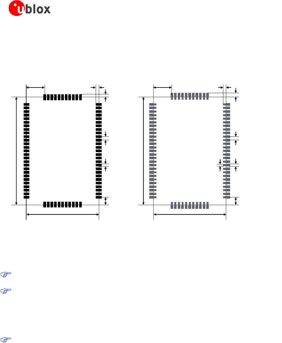
LISA-U1/LISA-H1 series - System Integration Manual
3G.G2-HW-10002-2 Advance Information Design-In
Page 93 of 116
2.2.2 Footprint and paste mask
The following figure describes the footprint and provides recommendations for the paste mask for LISA-U1/LISA-
H1 series modules. These are recommendations only and not specifications. Note that the copper and solder
masks have the same size and position.
33.2 mm [1307.1 mil]
22.4 mm [881.9 mil]
2.3 mm
[90.6 mil]
0.8 mm
[31.5 mil]
1.1 mm
[43.3 mil]
0.8 mm
[31.5 mil]
1.0 mm
[39.3 mil]
5.7 mm
[224.4 mil]
33.2 mm [1307.1 mil]
22.4 mm [881.9 mil]
2.3 mm
[90.6 mil]
1.2 mm
[47.2 mil]
1.1 mm
[43.3 mil]
0.8 mm
[31.5 mil]
0.9 mm
[35.4 mil]
5.7 mm
[224.4 mil]
0.6 mm
[23.6 mil]
Stencil: 120 µm
Figure 52: LISA-U1/LISA-H1 series modules suggested footprint and paste mask
To improve the wetting of the half vias, reduce the amount of solder paste under the module and increase the
volume outside of the module by defining the dimensions of the paste mask to form a T-shape (or equivalent)
extending beyond the copper mask. The solder paste should have a total thickness of 120 µm.
The paste mask outline needs to be considered when defining the minimal distance to the next
component.
The exact geometry, distances, stencil thicknesses and solder paste volumes must be adapted to the
specific production processes (e.g. soldering etc.) of the customer.
The bottom layer of LISA-U1/LISA-H1 series modules shows an unprotected copper area for GND described in
Figure 53.
Consider “No-routing” area for the LISA-U1/LISA-H1 series modules footprint as follows: signals keep-
out area on the top layer of the application board, below LISA-U1/LISA-H1 series modules, due to GND
opening on module bottom layer (see Figure 53).
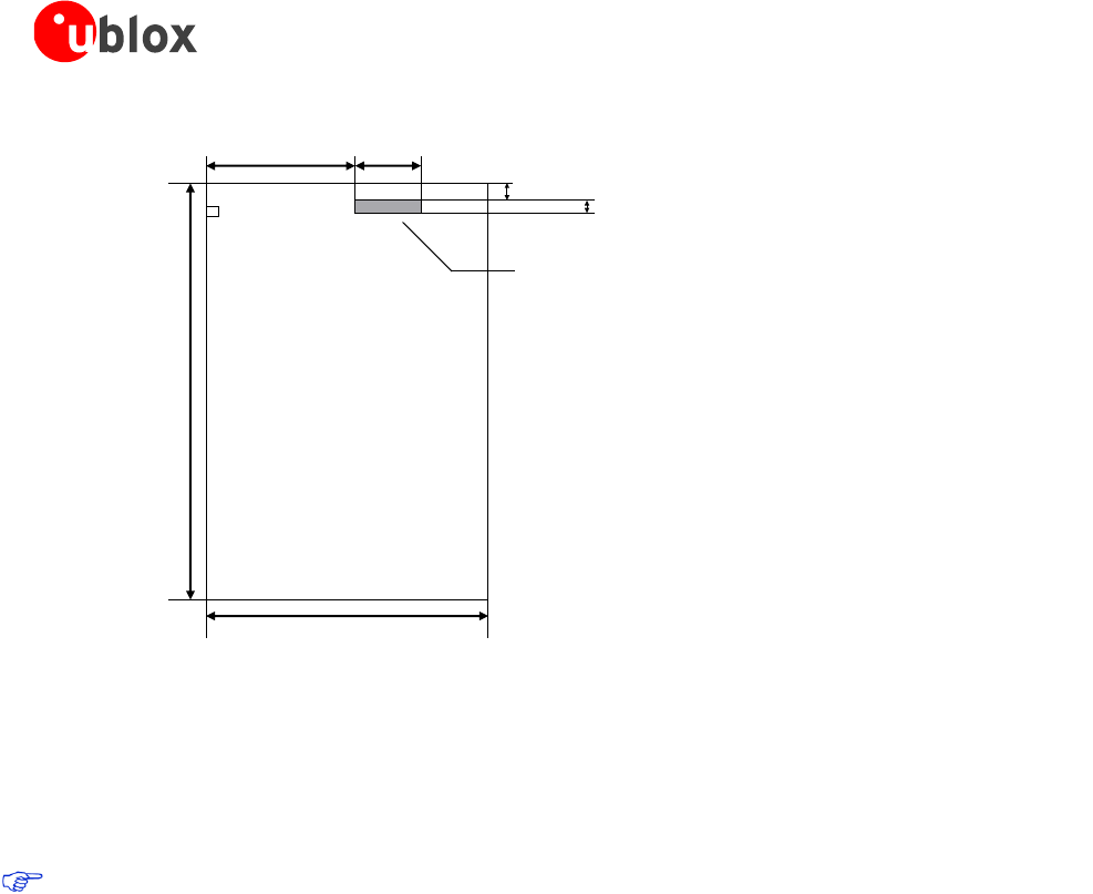
LISA-U1/LISA-H1 series - System Integration Manual
3G.G2-HW-10002-2 Advance Information Design-In
Page 94 of 116
5.3 mm11.85 mm
33.2 mm
1.0 mm
1.4 mm
PIN 1
Bottom side
(through module view)
22.40 mm
Exposed GND on LISA module bottom layer
Signals keep-out area on application board
Figure 53: Signals keep-out area on the top layer of the application board, below LISA-U1/LISA-H1 series modules
2.2.3 Placement
Optimize placement for minimum length of RF line and closer path from DC source for VCC.
The heat dissipation during continuous transmission at maximum power can significantly raise the
temperature of the application base-board below the LISA-U1/LISA-H1 series modules: avoid placing
temperature sensitive devices (e.g. GPS receiver) close to the module.

LISA-U1/LISA-H1 series - System Integration Manual
3G.G2-HW-10002-2 Advance Information Design-In
Page 95 of 116
2.3 Thermal aspects
The operating temperature range is specified in the LISA-U1/LISA-H1 series Data Sheet [1].
The most critical condition concerning thermal performance is the uplink transmission at maximum power (data
upload or voice call in connected mode), when the baseband processor runs at full speed, radio circuits are all
active and the RF power amplifier is driven to higher output RF power. This scenario is not often encountered in
real networks; however the application should be correctly designed to cope with it.
During transmission at maximum RF power the LISA-U1/LISA-H1 series modules generate thermal power that
can exceed 2 W: this is an indicative level since the exact generated power strictly depends on operating
condition such as the number of allocated TX slot and modulation (GMSK or 8PSK) or data rate (WCDMA),
transmitting frequency band, etc. The generated thermal power must be adequately dissipated through the
thermal and mechanical design of the application.
The increase of thermal dissipation, i.e. reducing the thermal resistance, will reduce the operating temperature
for internal circuitry of LISA-U1/LISA-H1 series modules for the same operating ambient temperature. This
improves the device long-term reliability for applications operating at high ambient temperature.
A few techniques may be used to reduce the thermal resistance in the application:
Forced ventilation air-flow within mechanical enclosure
Usage of thermal transfer material (e.g. greases and pastes)
Heat sink attached to the module top side, with electrically insulated / high thermal conductivity adhesive
Connect each GND pin with solid ground layer of the application board and connect each ground area of
the multilayer application board with complete via stack down to main ground layer

LISA-U1/LISA-H1 series - System Integration Manual
3G.G2-HW-10002-2 Advance Information Design-In
Page 96 of 116
2.4 Antenna guidelines
Antenna characteristics are essential for good functionality of the module. Antenna radiating performance has
direct impact on the reliability of connections over the Air Interface. A bad termination of ANT can result in poor
performance of the module.
The following parameters should be checked:
Item
Recommendations
Impedance
50 Ω nominal characteristic impedance
Frequency Range
Depends on the LISA-U1/LISA-H1 series module version and on the Mobile Network used.
LISA-U100/U120/H100:
- GSM 850: 824..894 MHz = UMTS B5: 824..894 MHz
- GSM 1900: 1850..1990 MHz = UMTS B2: 1850..1990 MHz
LISA-U110/U130/H110:
- GSM 900: 880..960 MHz = UMTS B8: 880..960 MHz
- GSM 1800: 1710..1880 MHz
- UMTS B1: 1920..2170 MHz
Input Power
>2 W peak
V.S.W.R
<2:1 recommended, <3:1 acceptable
Return Loss
S11<-10 dB recommended, S11<-6 dB acceptable
Gain
<3 dBi
Table 35: General recommendation for GSM antenna
To preserve the original u-blox FCC ID antenna gain shall remain below 3 dBi.
Please note that some 2G and 3G bands are overlapping. This depends on worldwide band allocation for
telephony services, where different bands are deployed for different geographical regions.
If the LISA-U110/U130 modules are planned for use on the entire supported bands, then a tri-band antenna
(880..960 MHz, 1710..1880 MHz, 1920..2170 MHz) should be selected. If the LISA-U100/U120 modules are
planned for use on the entire supported bands, then a dual-band antenna (824..894 MHz, 1850..1990 MHz)
should be selected. Otherwise, for fixed applications in specific geographical region, antenna requirements can
be relaxed for non-deployed frequency bands.
GSM antennas are typically available as:
Linear monopole: typical for fixed applications. The antenna extends mostly as a linear element with a
dimension comparable to lambda/4 of the lowest frequency of the operating band. Magnetic base may be
available. Cable or direct RF connectors are common options. The integration normally requires the
fulfillment of some minimum guidelines suggested by antenna manufacturer
Patch-like antenna: better suited for integration in compact designs (e.g. mobile phone). These are mostly
custom designs where the exact definition of the PCB and product mechanical design is fundamental for
tuning of antenna characteristics
For integration observe these recommendations:
Ensure 50 Ω antenna termination, minimize the V.S.W.R. or return loss, as this will optimize the electrical
performance of the module. See section 2.4.1
Select antenna with best radiating performance. See section 2.4.2
If a cable is used to connect the antenna radiating element to application board, select a short cable with
minimum insertion loss. The higher the additional insertion loss due to low quality or long cable, the lower
the connectivity
Follow the recommendations of the antenna manufacturer for correct installation and deployment
Do not include antenna within closed metal case
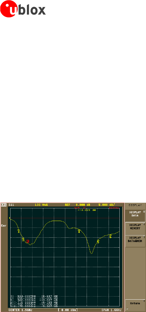
LISA-U1/LISA-H1 series - System Integration Manual
3G.G2-HW-10002-2 Advance Information Design-In
Page 97 of 116
Do not place antenna in close vicinity to end user since the emitted radiation in human tissue is limited by
S.A.R. regulatory requirements
Do not use directivity antenna since the electromagnetic field radiation intensity is limited in some countries
Take care of interaction between co-located RF systems since the GSM transmitted power may interact or
disturb the performance of companion systems
Place antenna far from sensitive analog systems or employ countermeasures to reduce electromagnetic
compatibility issues that may arise
2.4.1 Antenna termination
The LISA-U1/LISA-H1 series modules are designed to work on a 50 load. However, real antennas have no
perfect 50 load on all the supported frequency bands. Therefore, in order to as much as possible reduce
performance degradation due to antenna mismatch, the following requirements should be met:
Measure the antenna termination with a network analyzer: connect the antenna through a coaxial cable to the
measurement device, the |S11| indicates which portion of the power is delivered to antenna and which portion is
reflected by the antenna back to the module output.
A good antenna should have an |S11| below -10 dB over the entire frequency band. Due to miniaturization,
mechanical constraints and other design issues, this value will not be achieved. An |S11| value of about -6 dB - (in
the worst case) - is acceptable.
Figure 54 shows an example of this measurement:
Figure 54: |S11| sample measurement of a penta-band antenna that covers in a small form factor the 4 GSM bands (850 MHz, 900
MHz, 1800 MHz and 1900 MHz) and the UMTS Band I
Figure 55 shows comparable measurements performed on a wideband antenna. The termination is better, but
the size of the antenna is considerably larger.
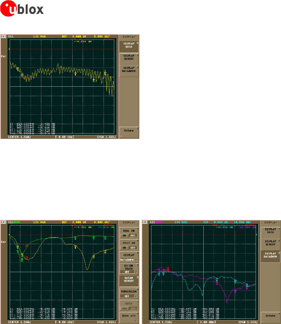
LISA-U1/LISA-H1 series - System Integration Manual
3G.G2-HW-10002-2 Advance Information Design-In
Page 98 of 116
Figure 55: |S11| sample measurement of a wideband antenna
2.4.2 Antenna radiation
An indication of the antenna’s radiated power can be approximated by measuring the |S21| from a target antenna
to the measurement antenna, using a network analyzer with a wideband antenna. Measurements should be
done at a fixed distance and orientation, and results compared to measurements performed on a known good
antenna. Figure 56 through Figure 57 show measurement results. A wideband log periodic-like antenna was
used, and the comparison was done with a half lambda dipole tuned at 900 MHz frequency. The measurements
show both the |S11| and |S21| for the penta-band internal antenna and for the wideband antenna.
Figure 56: |S11| and |S21| comparison between a 900 MHz tuned half wavelength dipole (green/purple) and a penta-band internal
antenna (yellow/cyan)
The half lambda dipole tuned at 900 MHz is known and has good radiation performance (both for gain and
directivity). Then, by comparing the |S21| measurement with antenna under investigation for the frequency where
the half dipole is tuned (e.g. marker 3 in Figure 56) it is possible to make a judgment on the antenna under test:
if the performance is similar then the target antenna is good.
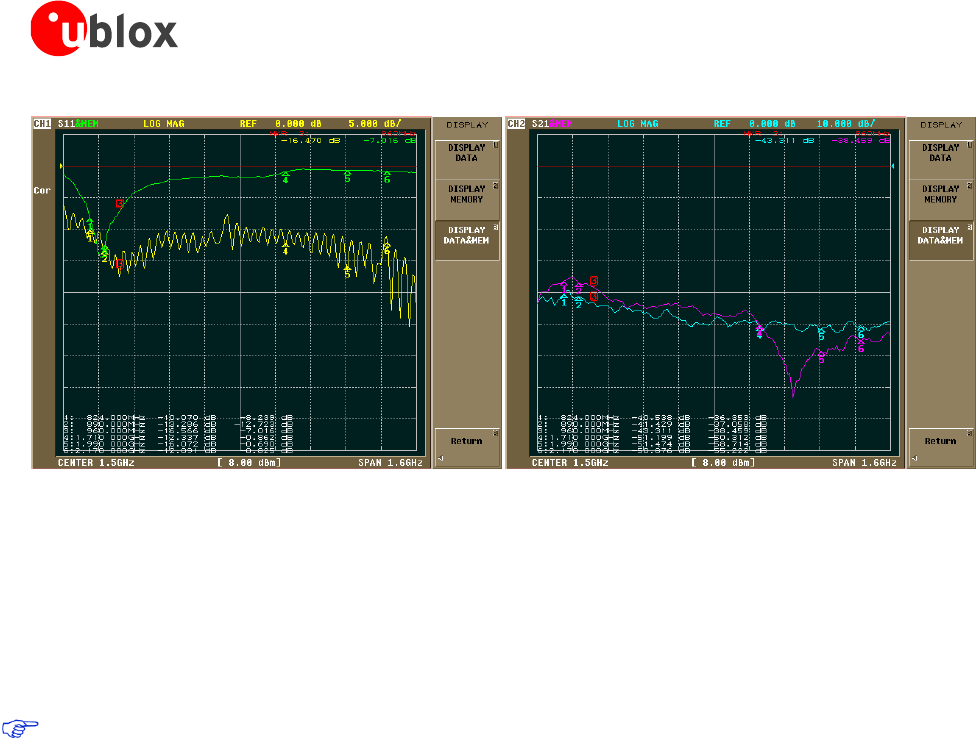
LISA-U1/LISA-H1 series - System Integration Manual
3G.G2-HW-10002-2 Advance Information Design-In
Page 99 of 116
Figure 57: |S11| and |S21| comparison between a 900 MHz tuned half wavelength dipole (green/purple) and a wideband
commercial antenna (yellow/cyan)
Instead if |S21| values for the tuned dipole are much better than the antenna under evaluation (like for marker 1/2
area of Figure 57, where dipole is 5 dB better), then it can be argued that the radiation of the target antenna
(the wideband dipole in this case) is considerably less.
The same procedure should be repeated on other bands with half wavelength dipole re-tuned to the band under
investigation.
For good antenna radiation performance, antenna dimensions should be comparable to a quarter of the
wavelength. Different antenna types can be used for the module, many of them (e.g. patch antennas,
monopole) are based on a resonating element that works in combination with a ground plane. The
ground plane, ideally infinite, can be reduced down to a minimum size that must be similar to one
quarter of the wavelength of the minimum frequency that has to be radiated (transmitted/received).
Numerical sample: frequency = 1 GHz wavelength = 30 cm minimum ground plane (or antenna
size) = 7.5 cm. Below this size, the antenna efficiency is reduced.
2.4.3 Antenna detection functionality
The internal antenna detect circuit is based on ADC measurement at ANT: the RF port is DC coupled to the ADC
unit in the baseband chip which injects a DC current (10 µA for 128 µs) on ANT and measures the resulting DC
voltage to evaluate the resistance from ANT pad to GND.
The antenna detection is forced by the +UANTR AT command: refer to the u-blox AT Commands Manual [2] for
more details on how to access this feature.
To achieve antenna detection functionality, use an RF antenna with built-in resistor from ANT signal to GND, or
implement an equivalent solution with a circuit between the antenna cable connection and the radiating
element as shown in Figure 58.
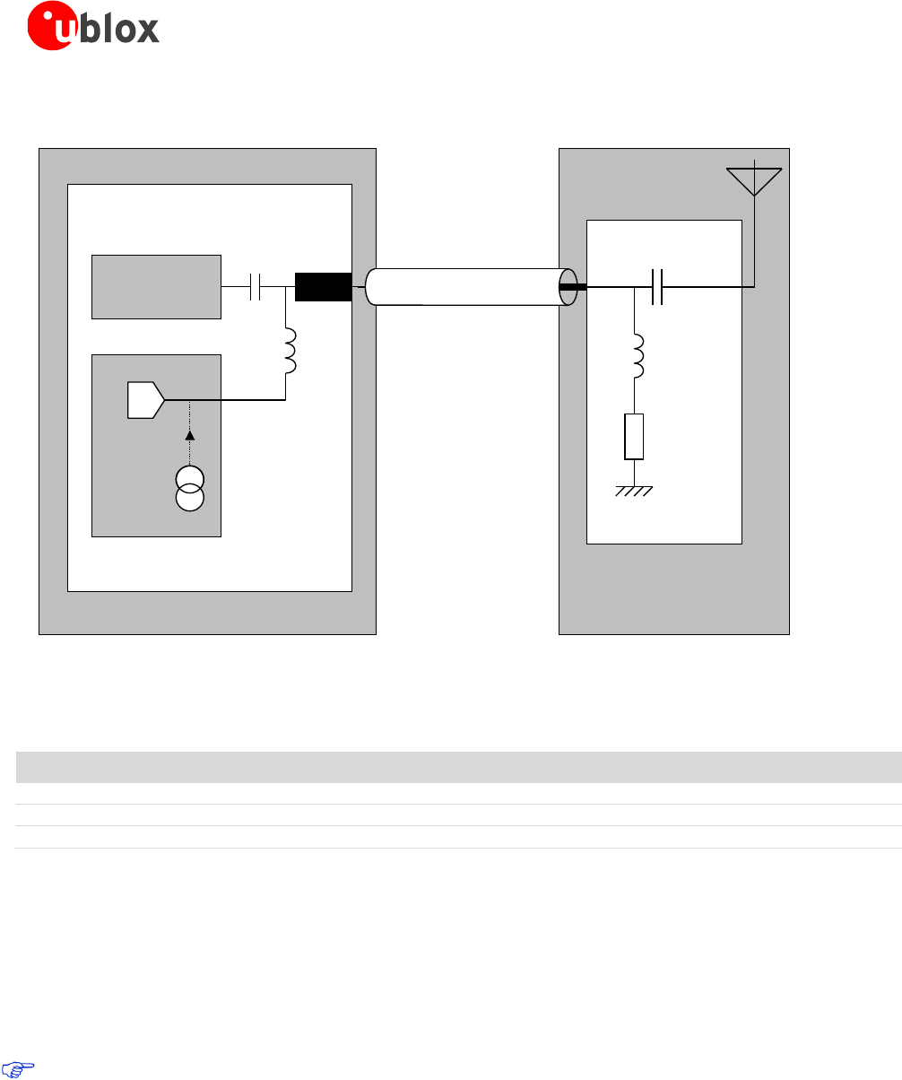
LISA-U1/LISA-H1 series - System Integration Manual
3G.G2-HW-10002-2 Advance Information Design-In
Page 100 of 116
Application Board Antenna Assembly
Diagnostic Circuit
LISA-U1/LISA-H1 series
ADC
Current
Source
RF
Choke
DC
Blocking
Front-End
RF Module
RF
Choke
DC
Blocking
Radiating
Element
Zo=50 Ω
Resistor for
Diagnostic
Coaxial Antenna Cable
ANT
Figure 58: Antenna detection circuit and antenna with diagnostic resistor
Examples of components for the antenna detection diagnostic circuit are reported in the following table:
Description
Part Number - Manufacturer
DC Blocking Capacitor
Murata GRM1555C1H220JA01 or equivalent
RF Choke Inductor
Murata LQG15HS68NJ02, LQG15HH68NJ02 or equivalent (Self Resonance Frequency ~1GHz)
Resistor for Diagnostic
15 k 5%, various Manufacturers
Table 36: Example of components for the antenna detection diagnostic circuit
Please note that the DC impedance at RF port for some antennas may be a DC open (e.g. linear monopole) or a
DC short to reference GND (e.g. PIFA antenna). For those antennas, without the diagnostic circuit of Figure 58,
the measured DC resistance will always be at the limits of the measurement range (respectively open or short),
and there will be no mean to distinguish between a defect on antenna path with similar characteristics
(respectively: removal of linear antenna or RF cable shorted to GND for PIFA antenna).
Furthermore, any other DC signal injected to the RF connection from ANT connector to radiating element will
alter the measurement and produce invalid results for antenna detection.
It is recommended to use an antenna with a built-in diagnostic resistor in the range from 5 kΩ to 30 kΩ
to assure good antenna detection functionality and to avoid a reduction of module RF performance. The
choke inductor should exhibit a parallel Self Resonance Frequency (SRF) in the range of 1 GHz to
improve the RF isolation of load resistor.
For example:
Consider a GSM antenna with built-in DC load resistor of 15 k. Using the +UANTR AT command, the module
reports the resistance value evaluated from ANT connector to GND:

LISA-U1/LISA-H1 series - System Integration Manual
3G.G2-HW-10002-2 Advance Information Design-In
Page 101 of 116
Reported values close to the used diagnostic resistor nominal value (i.e. values from 13 kΩ to 17 kΩ if a
15 kΩ diagnostic resistor is used) indicate that the antenna is properly connected
Values close to the measurement range maximum limit (approximately 50 kΩ) or an open-circuit
“over range” report (see u-blox AT Commands Manual [2]) means that that the antenna is not connected or
the RF cable is broken
Reported values below the measurement range minimum limit (1 kΩ) will highlight a short to GND at
antenna or along the RF cable
Measurement inside the valid measurement range and outside the expected range may indicate an improper
connection, damaged antenna or wrong value of antenna load resistor for diagnostic
Reported value could differ from the real resistance value of the diagnostic resistor mounted inside the
antenna assembly due to antenna cable length, antenna cable capacity and the used measurement method

LISA-U1/LISA-H1 series - System Integration Manual
3G.G2-HW-10002-2 Advance Information Design-In
Page 102 of 116
2.5 ESD immunity test precautions
The immunity to the EMS phenomenon Electrostatic Discharge of the device (i.e. the application board where
the LISA-U1/LISA-H1 series module is mounted) must be certified complying the testing requirements standard
[10] and the requirements for radio and digital cellular radio telecommunications system equipments standards
[11] [12].
The ESD test is performed at the enclosure port [11] referred as the physical boundary through which EM field
radiates. If the device implements an integral antenna [11] the enclosure is intended as all insulating surfaces
housing the device. If the device implements a removable antenna [11] the enclosure port is limited to the
antenna port [11] hence the enclosure port comprises the antenna element and its interconnecting cable
surfaces.
The applicability of the ESD test depends to the device classification [11], as well the test on other ports [11] or
on interconnecting cables to auxiliary equipments depends to the device accessible interfaces and manufacturer
requirements.
Contact discharges [10] are performed at conductive surfaces whereas air discharges [10] are performed at
insulating surfaces. Indirect contact discharges are performed on the measurement setup horizontal and vertical
coupling planes [10].
Some precautions should be implemented as described in the following sections in order to satisfy ESD immunity
test requirements [10] [11] [12] performed at device enclosure complying the category level [11] and shown in
the following table.
Category
Immunity Level
Contact Discharge to coupling planes (indirect contact discharge)
+2 kV / -2 kV
+4 kV / -4 kV
Contact Discharges to conducted surfaces (direct contact discharge)
Not Applicable2*
Air Discharge at insulating surfaces
+2 kV / -2 kV
+4 kV / -4 kV
+8 kV / -8 kV
Table 37: Enclosure ESD immunity level, standards “EN 61000-4-2, EN 301 489-1 V1.8.1, EN 301 489-7 V1.3.1”
2.5.1 General precautions
The following module interfaces could be involved in the ESD immunity test criticality depending on the
application board handling. Some precautions are herein suggested.
Sensitive interface is the reset line (RESET_N pin):
A 47 pF bypass capacitor (e.g. Murata GRM1555C1H470JA01) have to be mounted on the line termination
connected to the RESET_N pin to avoid a module reset caused by an electrostatic discharge applied to the
application board
A series ferrite bead (e.g. Murata BLM15HD182SN1) must be added on the line connected to the RESET_N
pin to avoid a module reset caused by an electrostatic discharge applied to the application board
2
LISA mounted on application reference design:
Applicability -> EUT with insulating surfaces, air discharges on interconnecting cables between EUT and antenna and auxiliary equipments
Not Applicability -> EUT with conductive surface, direct contact discharge
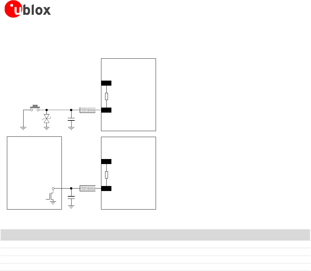
LISA-U1/LISA-H1 series - System Integration Manual
3G.G2-HW-10002-2 Advance Information Design-In
Page 103 of 116
It is recommended to keep the connection line to RESET_N as short as possible
LISA-U1/LISA-H1
series
2V_BCKP
22 RESET_N
Reset
push button
ESD
Open
Drain
Output
Application
Processor
LISA-U1/LISA-H1
series
2V_BCKP
22 RESET_N
Rint
Rint
FB1
C1
FB2
C2
Figure 59: RESET_N application circuits for ESD immunity test
Reference
Description
Remarks
ESD
Varistor for ESD protection.
CT0402S14AHSG - EPCOS
C1, C2
47 pF Capacitor Ceramic C0G 0402 5% 50 V
GRM1555C1H470JA01 - Murata
FB1, FB2
Chip Ferrite Bead for Noise/EMI Suppression
BLM15HD182SN1 - Murata
Rint
10 kΩ Resistor 0402 5% 0.1 W
Internal pull-up resistor
Table 38: Example of components as ESD immunity test precautions for the RESET_N line
Sensitive interface is the SIM interface (VSIM pin, SIM_RST pin, SIM_IO pin, SIM_CLK pin):
A 47 pF bypass capacitor (e.g. Murata GRM1555C1H470J) have to be mounted on the lines connected to
VSIM, SIM_RST, SIM_IO and SIM_CLK to assure SIM interface functionality when an electrostatic discharge
is applied to the application board
It is suggested to use as short as possible connection lines at SIM pins
2.5.2 Antenna interface precautions
The antenna interface ANT could be involved in the ESD immunity test criticality depending on the application
board handling. Antenna precaution is herein suggested.
If the device implements an embedded antenna and the device insulating enclosure avoids air discharge up
to +8 kV / -8 kV to the antenna interface, no further precautions to ESD immunity test should be needed
If the device implements an external antenna and the antenna and its connecting cable are provided with a
completely insulating enclosure to avoid air discharge up to +8 kV / -8 kV to the whole antenna and cable
surfaces, no further precautions to ESD immunity test should be needed

LISA-U1/LISA-H1 series - System Integration Manual
3G.G2-HW-10002-2 Advance Information Design-In
Page 104 of 116
If the device implements an external antenna and the antenna or its connecting cable are not provided with
completely insulating enclosure to avoid air discharge up to +8 kV / -8 kV to the whole antenna and cable
surfaces, precautions to ESD immunity test should be implemented on the application board
A higher protection level is required at the ANT port if the line is externally accessible on the application board.
2.5.3 Module interfaces precautions
All the module pins that are externally accessible should be included in the ESD immunity test since they are
considered to be a port [11]. Depending on applicability, and in order to satisfy ESD immunity test requirements
and ESD category level, pins connected to the port should be protected up to +4 kV / -4 kV for direct Contact
Discharge, and up to +8 kV / -8 kV for Air Discharge applied to the enclosure.
The maximum ESD rating of all the pins of the module, except the ANT pin, is 1 kV (HBM according MIL-Std
883D, method 3015.7, EOS/ESD Standard S5.1-1993). A higher protection level can be achieved by mounting an
ESD protection (e.g. EPCOS CA05P4S14THSG varistor array).

LISA-U1/LISA-H1 series - System Integration Manual
3G.G2-HW-10002-2 Advance Information Handling and soldering
Page 105 of 116
3 Handling and soldering
No natural rubbers, no hygroscopic materials or materials containing asbestos are employed.
3.1 Packaging, shipping, storage and moisture preconditioning
For information pertaining to reels and tapes, Moisture Sensitivity levels (MSD), shipment and storage
information, as well as drying for preconditioning see the LISA-U1/LISA-H1 series Data Sheet [1].
The LISA-U1/LISA-H1 series modules are Electro-Static Discharge (ESD) sensitive devices.
Ensure ESD precautions are implemented during handling of the module.
3.2 Soldering
3.2.1 Soldering paste
Use of "No Clean" soldering paste is strongly recommended, as it does not require cleaning after the soldering
process has taken place. The paste listed in the example below meets these criteria.
Soldering Paste: OM338 SAC405 / Nr.143714 (Cookson Electronics)
Alloy specification: 95.5% Sn / 3.9% Ag / 0.6% Cu (95.5% Tin / 3.9% Silver / 0.6% Copper)
95.5% Sn / 4.0% Ag / 0.5% Cu (95.5% Tin / 4.0% Silver / 0.5% Copper)
Melting Temperature: 217°C
Stencil Thickness: 120 µm for base boards
The final choice of the soldering paste depends on the approved manufacturing procedures.
The paste-mask geometry for applying soldering paste should meet the recommendations in section 2.2.2
The quality of the solder joints on the connectors (’half vias’) should meet the appropriate IPC
specification.
3.2.2 Reflow soldering
A convection type-soldering oven is strongly recommended over the infrared type radiation oven.
Convection heated ovens allow precise control of the temperature and all parts will be heated up evenly,
regardless of material properties, thickness of components and surface color.
Consider the "IPC-7530 Guidelines for temperature profiling for mass soldering (reflow and wave) processes,
published 2001".
Preheat phase
Initial heating of component leads and balls. Residual humidity will be dried out. Please note that this preheat
phase will not replace prior baking procedures.
Temperature rise rate: max 3°C/s If the temperature rise is too rapid in the preheat phase it may cause
excessive slumping.
Time: 60 – 120 s If the preheat is insufficient, rather large solder balls tend to be
generated. Conversely, if performed excessively, fine balls and large
balls will be generated in clusters.
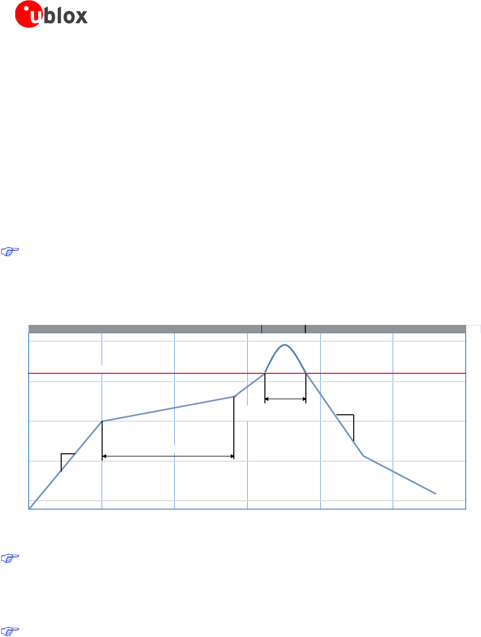
LISA-U1/LISA-H1 series - System Integration Manual
3G.G2-HW-10002-2 Advance Information Handling and soldering
Page 106 of 116
End Temperature: 150 - 200°C If the temperature is too low, non-melting tends to be caused in
areas containing large heat capacity.
Heating/ reflow phase
The temperature rises above the liquidus temperature of 217°C. Avoid a sudden rise in temperature as the slump
of the paste could become worse.
Limit time above 217°C liquidus temperature: 40 - 60 s
Peak reflow temperature: 245°C
Cooling phase
A controlled cooling avoids negative metallurgical effects (solder becomes more brittle) of the solder and
possible mechanical tensions in the products. Controlled cooling helps to achieve bright solder fillets with a good
shape and low contact angle.
Temperature fall rate: max 4°C / s
To avoid falling off, modules should be placed on the topside of the motherboard during soldering.
The final soldering temperature chosen at the factory depends on additional external factors like choice of
soldering paste, size, thickness and properties of the base board, etc. Exceeding the maximum soldering
temperature in the recommended soldering profile may permanently damage the module.
Preheat Heating Cooling
[°C] Peak Temp. 245°C [°C]
250 250
Liquidus Temperature
217 217
200 200
40 - 60 s
End Temp.
max 4°C/s
150 - 200°C
150 150
max 3°C/s
60 - 120 s
100 Typical Leadfree 100
Soldering Profile
50 50
050 100 150 200 250 300
Elapsed time [s]
Figure 60: Recommended soldering profile
When soldering lead-free LISA-U1/LISA-H1 series modules in a leaded process, check the following
temperatures:
PB- Technology Soaktime: 40-80 s
Time above Liquidus: 40-90 s
Peak temperature: 225-235°C
LISA-U1/LISA-H1 series modules must not be soldered with a damp heat process.

LISA-U1/LISA-H1 series - System Integration Manual
3G.G2-HW-10002-2 Advance Information Handling and soldering
Page 107 of 116
3.2.3 Optical inspection
After soldering the LISA-U1/LISA-H1 series modules, inspect the modules optically to verify that he module is
properly aligned and centered.
3.2.4 Cleaning
Cleaning the soldered modules is not recommended. Residues underneath the modules cannot be easily
removed with a washing process.
Cleaning with water will lead to capillary effects where water is absorbed in the gap between the baseboard
and the module. The combination of residues of soldering flux and encapsulated water leads to short circuits
or resistor-like interconnections between neighboring pads. Water will also damage the sticker and the ink-
jet printed text.
Cleaning with alcohol or other organic solvents can result in soldering flux residues flooding into the two
housings, areas that are not accessible for post-wash inspections. The solvent will also damage the sticker
and the ink-jet printed text.
Ultrasonic cleaning will permanently damage the module, in particular the quartz oscillators.
For best results use a "no clean" soldering paste and eliminate the cleaning step after the soldering.
3.2.5 Repeated reflow soldering
Only a single reflow soldering process is encouraged for boards with a LISA-U1/LISA-H1 series module populated
on it. The reason for this is the risk of the module falling off due to high weight in relation to the adhesive
properties of the solder.
3.2.6 Wave soldering
Boards with combined through-hole technology (THT) components and surface-mount technology (SMT) devices
require wave soldering to solder the THT components. Only a single wave soldering process is encouraged for
boards populated with LISA-U1/LISA-H1 series modules.
3.2.7 Hand soldering
Hand soldering is not recommended.
3.2.8 Rework
The LISA-U1/LISA-H1 series modules can be unsoldered from the baseboard using a hot air gun.
Avoid overheating the module.
After the module is removed, clean the pads before placing.
Never attempt a rework on the module itself, e.g. replacing individual components. Such
actions immediately terminate the warranty.
3.2.9 Conformal coating
Certain applications employ a conformal coating of the PCB using HumiSeal® or other related coating products.
These materials affect the HF properties of the LISA-U1/LISA-H1 series modules and it is important to prevent
them from flowing into the module.
The RF shields do not provide 100% protection for the module from coating liquids with low viscosity, therefore
care is required in applying the coating.
Conformal Coating of the module will void the warranty.

LISA-U1/LISA-H1 series - System Integration Manual
3G.G2-HW-10002-2 Advance Information Handling and soldering
Page 108 of 116
3.2.10 Casting
If casting is required, use viscose or another type of silicon pottant. The OEM is strongly advised to qualify such
processes in combination with the LISA-U1/LISA-H1 series modules before implementing this in the production.
Casting will void the warranty.
3.2.11 Grounding metal covers
Attempts to improve grounding by soldering ground cables, wick or other forms of metal strips directly onto the
EMI covers is done at the customer's own risk. The numerous ground pins should be sufficient to provide
optimum immunity to interferences and noise.
u-blox gives no warranty for damages to the LISA-U1/LISA-H1 series modules caused by soldering metal
cables or any other forms of metal strips directly onto the EMI covers.
3.2.12 Use of ultrasonic processes
Some components on the LISA-U1/LISA-H1 series modules are sensitive to Ultrasonic Waves. Use of any
Ultrasonic Processes (cleaning, welding etc.) may cause damage to the module.
u-blox gives no warranty against damages to the LISA-U1/LISA-H1 series modules caused by any
Ultrasonic Processes.
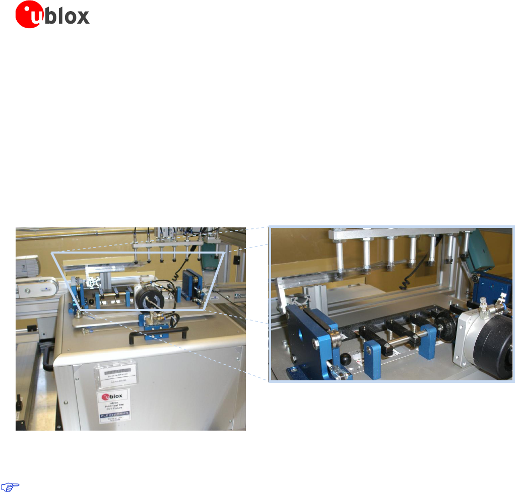
LISA-U1/LISA-H1 series - System Integration Manual
3G.G2-HW-10002-2 Advance Information Product Testing
Page 109 of 116
4 Product Testing
4.1 u-blox in-series production test
u-blox focuses on high quality for its products. All units produced are fully tested. Defective units are analyzed in
detail to improve the production quality.
This is achieved with automatic test equipment, which delivers a detailed test report for each unit. The following
measurements are done:
Digital self-test (Software Download, verification of FLASH firmware, etc.)
Measurement of voltages and currents
Measurement of RF characteristics
Figure 61: Automatic test equipment for module tests
4.2 Test parameters for OEM manufacturer
The chapter will be completed in the next releases.

LISA-U1/LISA-H1 series - System Integration Manual
3G.G2-HW-10002-2 Advance Information Appendix
Page 110 of 116
Appendix
A Extra Features
A.1 TCP/IP
Via the AT commands it’s possible to access the TCP/IP functionalities over the GPRS connection. For more
details about AT commands see the u-blox AT Commands Manual [2].
A.1.1 Multiple IP addresses and sockets
Using LISA’s embedded TCP/IP or UDP/IP stack, only 1 IP instance (address) is supported. The IP instance supports
up to 16 sockets. Using an external TCP/IP stack (on the application processor), it is possible to have 2 IP
instances (addresses).
A.2 FTP
LISA-U1/LISA-H1 series modules will support this feature in the upcoming version.
A.3 FTPS
LISA-U1/LISA-H1 series modules will support this feature in the upcoming version.
A.4 HTTP
LISA-U1/LISA-H1 series modules will support this feature in the upcoming version.
A.5 HTTPS
LISA-U1/LISA-H1 series modules will support this feature in the upcoming version.
A.6 SMTP
LISA-U1/LISA-H1 series modules will support this feature in the upcoming version.
A.7 AssistNow clients and GPS integration
For customers using u-blox GPS receivers, LISA-U1/LISA-H1 series modules feature embedded AssistNow Online
and AssistNow Offline clients. AssistNow A-GPS provides better GPS performance and faster Time-To-First-Fix.
The clients can be enabled / disabled with an AT command.
LISA-U1/LISA-H1 series modules act as a stand-alone AssistNow client, making AssistNow available with no
additional requirements for resources or software integration on an external host micro controller. Full access to
u-blox GPS receivers is available via the LISA-U1/LISA-H1 series, through a dedicated DDC (I2C) interface, while
the available GPIOs can handle the GPS device power on/off. This means that GSM/EDGE and GPS can be
controlled through a single serial port from any host processor.
A.8 In-Band modem (LISA-U130 only)
LISA-U130 Automotive grade version implements the in-Band modem solution for eCall according to the 3GPP
TS 26.267 specification [13].
According to the eCall (Pan-European automatic in-vehicle emergency call system) specification, an eCall must
be generated automatically or manually following an car accident using GSM cellular service “112”. When
activated, the in-vehicle eCall system (IVS) creates an emergency call carrying both voice and data (e.g. vehicle
GPS position) directly to the nearest 112 Public Safety Answering Point (PSAP) to quickly decide upon detaching
rescue services to the known position.
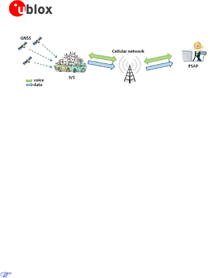
LISA-U1/LISA-H1 series - System Integration Manual
3G.G2-HW-10002-2 Advance Information Appendix
Page 111 of 116
Figure 62: In-Band modem diagram flow
In-band modem allows the fast and reliable transmission of vehicle Minimum Set of Data (MSD - 140 bytes) and
the establishment of a voice emergency call using the same physical channel (voice channel) without any
modifications of the existing cellular network architecture.
In-Band modem is a mandatory feature to meet the eCall requirements and to develop in vehicle devices fully
supporting eCall.
The in-Band modem functionality is delivered upon request.
A.9 Smart temperature supervision
An internal sensor is used to constantly monitor the board temperature of the LISA-U1/LISA-H1 series modules.
The measured value is compared with the internally predefined thresholds and it proceeds accordingly.
A warning notification is reported by the module when the temperature value is still inside the valid range (i.e.
the module is still in a valid and good working condition) but it is close to the limit (upper or lower).
A shutdown is notified and automatically forced by the module when the temperature value is outside the
specified range (i.e. the module is in a dangerous working condition). For security reasons the shutdown is
suspended in case of emergency call in progress: in this case the device will switch off at call termination.
The Smart Temperature Supervisor feature can be enabled or disabled through an AT command (for more details
please to u-blox AT commands manual [2], +USTS AT command). If the feature is disabled there is no embedded
protection against not allowed temperature working conditions.
The sensor measures board temperature inside the shields, which can differ from ambient temperature.

LISA-U1/LISA-H1 series - System Integration Manual
3G.G2-HW-10002-2 Advance Information Appendix
Page 112 of 116
B Glossary
ADC
Analog to Digital Converter
AP
Application Processor
AT
AT Command Interpreter Software Subsystem, or attention
CBCH
Cell Broadcast Channel
CS
Coding Scheme
CSD
Circuit Switched Data
CTS
Clear To Send
DC
Direct Current
DCD
Data Carrier Detect
DCE
Data Communication Equipment
DCS
Digital Cellular System
DDC
Display Data Channel
DSP
Digital Signal Processing
DSR
Data Set Ready
DTE
Data Terminal Equipment
DTM
Dual Transfer Mode
DTR
Data Terminal Ready
EBU
External Bus Interface Unit
EDGE
Enhanced Data rates for GSM Evolution
E-GPRS
Enhanced GPRS
FDD
Frequency Division Duplex
FEM
Front End Module
FOAT
Firmware Over AT commands
FTP
File Transfer Protocol
FTPS
FTP Secure
GND
Ground
GPIO
General Purpose Input Output
GPRS
General Packet Radio Service
GPS
Global Positioning System
GSM
Global System for Mobile Communication
HF
Hands-free
HSDPA
High Speed Downlink Packet Access
HTTP
HyperText Transfer Protocol
HTTPS
Hypertext Transfer Protocol over Secure Socket Layer
HW
Hardware
I/Q
In phase and Quadrature
I2C
Inter-Integrated Circuit
I2S
Inter IC Sound
IP
Internet Protocol
IPC
Inter Processor Communication
LNA
Low Noise Amplifier

LISA-U1/LISA-H1 series - System Integration Manual
3G.G2-HW-10002-2 Advance Information Appendix
Page 113 of 116
MCS
Modulation Coding Scheme
NOM
Network Operating Mode
PA
Power Amplifier
PBCCH
Packet Broadcast Control Channel
PCM
Pulse Code Modulation
PCS
Personal Communications Service
PFM
Pulse Frequency Modulation
PMU
Power Management Unit
RF
Radio Frequency
RI
Ring Indicator
RTC
Real Time Clock
RTS
Request To Send
RXD
RX Data
SAW
Surface Acoustic Wave
SIM
Subscriber Identification Module
SMS
Short Message Service
SMTP
Simple Mail Transfer Protocol
SPI
Serial Peripheral Interface
SRAM
Static RAM
TCP
Transmission Control Protocol
TDMA
Time Division Multiple Access
TXD
TX Data
UART
Universal Asynchronous Receiver-Transmitter
UDP
User Datagram Protocol
UMTS
Universal Mobile Telecommunications System
USB
Universal Serial Bus
UTRA
UMTS Terrestrial Radio Access
VC-TCXO
Voltage Controlled - Temperature Compensated Crystal Oscillator
WCDMA
Wideband CODE Division Multiple Access

LISA-U1/LISA-H1 series - System Integration Manual
3G.G2-HW-10002-2 Advance Information Related documents
Page 114 of 116
Related documents
[1] u-blox LISA-U1/LISA-H1 series Data Sheet, Docu No 3G.G1-HW-10001
[2] u-blox AT Commands Manual, Docu No WLS-SW-11000
[3] ITU-T Recommendation V.24, 02-2000. List of definitions for interchange circuits between data
terminal equipment (DTE) and data circuit-terminating equipment (DCE).
http://www.itu.int/rec/T-REC-V.24-200002-I/en
[4] 3GPP TS 27.007 - AT command set for User Equipment (UE) (Release 1999)
[5] 3GPP TS 27.005 - Use of Data Terminal Equipment - Data Circuit terminating; Equipment (DTE - DCE)
interface for Short Message Service (SMS) and Cell Broadcast Service (CBS) (Release 1999)
[6] 3GPP TS 27.010 - Terminal Equipment to User Equipment (TE-UE) multiplexer protocol (Release 1999)
[7] Universal Serial Bus Revision 2.0 specification, http://www.usb.org/developers/docs/
[8] I2C-Bus Specification Version 2.1 Philips Semiconductors (January 2000),
http://www.nxp.com/acrobat_download/literature/9398/39340011_21.pdf
[9] RFC3267 - Real-Time Transport Protocol (RTP) Payload Format and File Storage, Format for the
Adaptive Multi-Rate (AMR) and Adaptive Multi-Rate Wideband (AMR-WB) Audio Codecs
[10] CENELEC EN 61000-4-2 (2001): "Electromagnetic compatibility (EMC) - Part 4-2: Testing and
measurement techniques - Electrostatic discharge immunity test".
[11] ETSI EN 301 489-1 V1.8.1: “Electromagnetic compatibility and Radio spectrum Matters (ERM);
ElectroMagnetic Compatibility (EMC) standard for radio equipment and services; Part 1: Common
technical requirements”
[12] ETSI EN 301 489-7 V1.3.1 “Electromagnetic compatibility and Radio spectrum Matters (ERM);
ElectroMagnetic Compatibility (EMC) standard for radio equipment and services; Part 7: Specific
conditions for mobile and portable radio and ancillary equipment of digital cellular radio
telecommunications systems (GSM and DCS)“
[13] 3GPP TS 26.267 - Technical Specification Group Services and System Aspects; eCall Data Transfer; In-
band modem solution; General description (Release 9)
[15] GSM Mux Implementation Application Note, Docu No WLS-CS-11002
[17] Firmware Update Application Note, Docu No WLS-CS-11001
[18] SPI Interface application Note, Docu No 3G.G2-CS-11000
Some of the above documents can be downloaded from u-blox web-site (http://www.u-blox.com).
Revision history
Revision
Date
Name
Status / Comments
-
21/10/2010
sses
Initial Release
1
11/01/2011
sses
Thickness information added
GPIO description improved
2
26/04/2011
lpah
Update to Advance Information status
and paste mask

LISA-U1/LISA-H1 series - System Integration Manual
3G.G2-HW-10002-2 Advance Information
Page 115 of 116

LISA-U1/LISA-H1 series - System Integration Manual
3G.G2-HW-10002-2 Advance Information Contact
Page 116 of 116
Contact
For complete contact information visit us at www.u-blox.com
u-blox Offices
North, Central and South America
u-blox America, Inc.
Phone: +1 (703) 483 3180
E-mail: info_us@u-blox.com
Regional Office West Coast:
Phone: +1 (703) 483 3184
E-mail: info_us@u-blox.com
Technical Support:
Phone: +1 (703) 483 3185
E-mail: support_us@u-blox.com
Headquarters
Europe, Middle East, Africa
u-blox AG
Phone: +41 44 722 74 44
E-mail: info@u-blox.com
Support: support @u-blox.com
Asia, Australia, Pacific
u-blox Singapore Pte. Ltd.
Phone: +65 6734 3811
E-mail: info_ap@u-blox.com
Support: support_ap@u-blox.com
Regional Office China:
Phone: +86 10 68 133 545
E-mail: info_cn@u-blox.com
Support: support_cn@u-blox.com
Regional Office Japan:
Phone: +81 3 5775 3850
E-mail: info_jp@u-blox.com
Support: support_jp@u-blox.com
Regional Office Korea:
Phone: +82 2 542 0861
E-mail: info_kr@u-blox.com
Support: support_kr@u-blox.com
Regional Office Taiwan:
Phone: +886 2 2657 1090
E-mail: info_tw@u-blox.com
Support: support_tw@u-blox.com
and paste mask
and paste mask