u blox NINAB1 Bluetooth module NINAB1 User Manual NINA B1 series
u-blox AG Bluetooth module NINAB1 NINA B1 series
UserManual.wiki
>
u blox
>
NINAB1 User Manual
User Manual
Navigation menu
Upload a User Manual
Namespaces
Wiki Guide
HTML
PDF
Info
Views
User Manual
Discussion / Help
Navigation
![NINA-B1 series - Data Sheet UBX-15019243 - R05 Early Production Information Functional description Page 8 of 35 1.5 AT command support You can configure NINA-B1 modules through u-blox s-center toolbox software using AT commands. The s-center evaluation software is available free of charge and can be downloaded from the u-blox website. 1.6 Supported features Feature Description BLE v4.2 stack Embedded Bluetooth low energy stack for next generation Bluetooth solutions. GATT based services The u-blox Low Energy Serial Port Service as well as generic GATT server and GATT client services. NINA-B11x firmware Includes the u-blox Serial Port Service and allows configuration of the module using AT commands sent over the UART interface. Firmware update Over The Air (FOTA) Firmware module update over a wireless connection using BLE. Firmware update Over AT command (FOAT) Firmware module update over AT command interfaces (UART). The feature can be enabled and configured using AT commands. Power saving The NINA-B1 series modules support different power saving modes. The power saving configuration is by default disabled, but it can be enabled and configured using AT commands. See section 2.3 and the NINA-B1 series System Integration Manual [1] for more information on the different power saving modes. Battery monitor Can be used to read the voltage of the VCC pin and will automatically issue warnings and/or power-down the module if the voltage is too low. Android connectivity Supports Bluetooth low energy connections with Android devices (Android 4.3 & higher) iOS connectivity Supports Bluetooth low energy connections with iOS devices Table 3: NINA-B1 main supported features](https://usermanual.wiki/u-blox/NINAB1/User-Guide-3113481-Page-8.png)
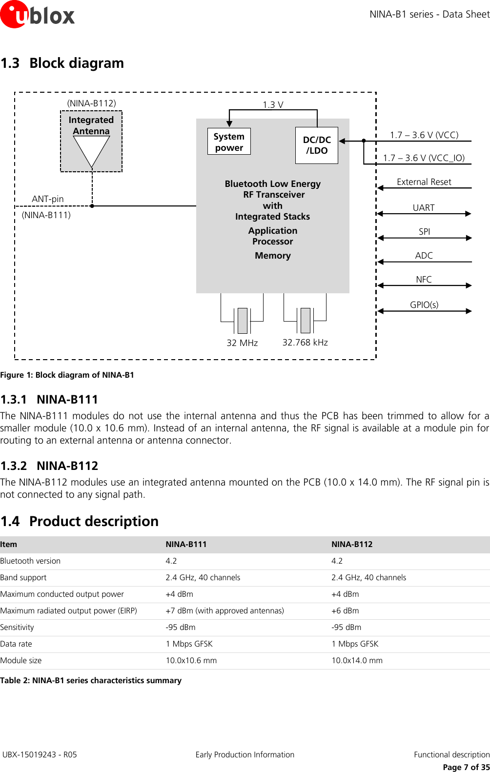
![NINA-B1 series - Data Sheet UBX-15019243 - R05 Early Production Information Interfaces Page 9 of 35 2 Interfaces 2.1 Power management 2.1.1 Module supply input (VCC) The NINA-B1 series uses an integrated DC/DC converter to transform the supply voltage presented at the VCC pin into a stable system voltage. Due to this, the NINA-B1 modules are compatible for use in battery powered designs. 2.1.2 Digital I/O interfaces reference voltage (VCC_IO) All modules in the u-blox NINA series provide an additional voltage supply input for setting the I/O voltage level. On the NINA-B1 series modules, the I/O voltage level is the same as the supply voltage and VCC_IO is internally connected to the supply input. Therefore only a single supply voltage is needed for NINA-B1, which makes it ideal for battery powered designs. This may not be the case for modules in the NINA series that will be released in the future. A design that should be pin compatible with other NINA-series modules should keep the VCC and VCC_IO supply rails separate. 2.2 RF antenna interfaces 2.2.1 2.4 GHz Bluetooth low energy (ANT) The two NINA-B1 model versions have their own 2.4 GHz antenna solutions respectively: The NINA-B111 modules provide an antenna pin (ANT) with a nominal characteristic impedance of 50 Ω. This pin can be connected to an on-board antenna or antenna connector using a controlled impedance trace. See the NINA-B1 series System Integration Manual [1] for more information. The NINA-B112 modules use an integrated antenna solution; no additional components are required. The ANT pin is internally disconnected on these models. 2.2.2 Near Field Communication (NFC) The NINA-B1 series modules include a Near Field Communication interface, capable of operating as a 13.56 MHz NFC tag at a bit rate of 106 kbps. As an NFC tag, data can be read from or written to the NINA-B1 modules using an NFC reader; however the NINA-B1 modules are not capable of reading other tags or initiating NFC communications. Two pins are available for connecting to an external NFC antenna: NFC1 and NFC2. See the NINA-B1 series System Integration Manual [1] for more information and NFC antenna design considerations. 2.3 System functions The NINA-B1 series modules are power efficient devices capable of operating in different power saving modes and configurations. Different sections of the module can be powered off when not needed and complex wake up events can be generated from different external and internal inputs. The radio part of the module operates independently from the CPU. The two main power saving modes are: Standby mode Sleep mode Depending on the application, the module should spend most of its time in sleep mode to conserve battery life. 2.3.1 Module power-on NINA-B1 modules can be switched on in one of the following ways and this will cause the module to reboot: Rising edge on the VCC pin to a valid supply voltage](https://usermanual.wiki/u-blox/NINAB1/User-Guide-3113481-Page-9.png)
![NINA-B1 series - Data Sheet UBX-15019243 - R05 Early Production Information Interfaces Page 10 of 35 Issuing a reset of the module A wake up event from sleep mode to active mode can be issued by: Changing the state of any digital I/O pin, may be enabled /disabled for each pin. If waking up from standby mode, an event can also be issued by: The on-board Real Time Counter (RTC) A programmable digital or analog sensor event. For example, rising voltage level on an analog comparator pin 2.3.2 Module power-off There is no dedicated pin to power off the NINA-B1 modules. You can configure any GPIO pin to enter or exit the sleep mode (see section 2.3.4), which essentially powers down the module. An under-voltage (brown-out) shutdown occurs on NINA-B1 modules when the VCC supply drops below the operating range minimum limit. If this occurs, it is not possible to store the current parameter settings in the module’s non-volatile memory. An over-temperature and under-temperature shutdown can be enabled on NINA-B1 modules, and is initiated if the temperature measured within the module is outside operating conditions. The temperature is measured by an integrated temperature sensor in the radio chip. For more details see the NINA-B1 series System Integration Manual [1]. 2.3.3 Standby mode Standby mode is one of the power saving modes in NINA-B1 modules that essentially powers down the module but keeps the system RAM intact and allows for a few low power digital interfaces (including SPI) and analog functions to run continuously. It also allows for more complex, autonomous power-up events including periodic RTC events and radio events. The following events can be used to bring the module out of the standby mode: External wake-up events Internal wake-up events from RTC, radio, NFC and so on Analog or digital sensor event (programmable voltage level or edge detection) During standby mode, the module is clocked at 32 kHz, which is generated by an internal 32 kHz crystal oscillator. 2.3.4 Sleep mode Sleep mode is the deepest power saving mode of NINA-B1 modules. During sleep mode, all functionality is stopped to ensure minimum power consumption. The module needs an external event in order to wake up from sleep mode. The following events can be used to wake up the module out of the sleep mode: External event on a digital pin External event on a low power comparator pin Detection of NFC field When using the NINA-B11x firmware, the module can be manually switched on or off with proper storage of current settings using the UART DSR pin. The module can be programmed to latch the digital values present at its GPIO pins during sleep. The module will keep the values latched, and a change of state on any of these pins will trigger a wake up to active mode. The module will always reboot after waking up from the sleep mode; however different sections of the RAM can be configured to remain intact during and after going into the sleep mode. 2.3.5 Module reset NINA-B1 modules can be reset in one of the following ways:](https://usermanual.wiki/u-blox/NINAB1/User-Guide-3113481-Page-10.png)
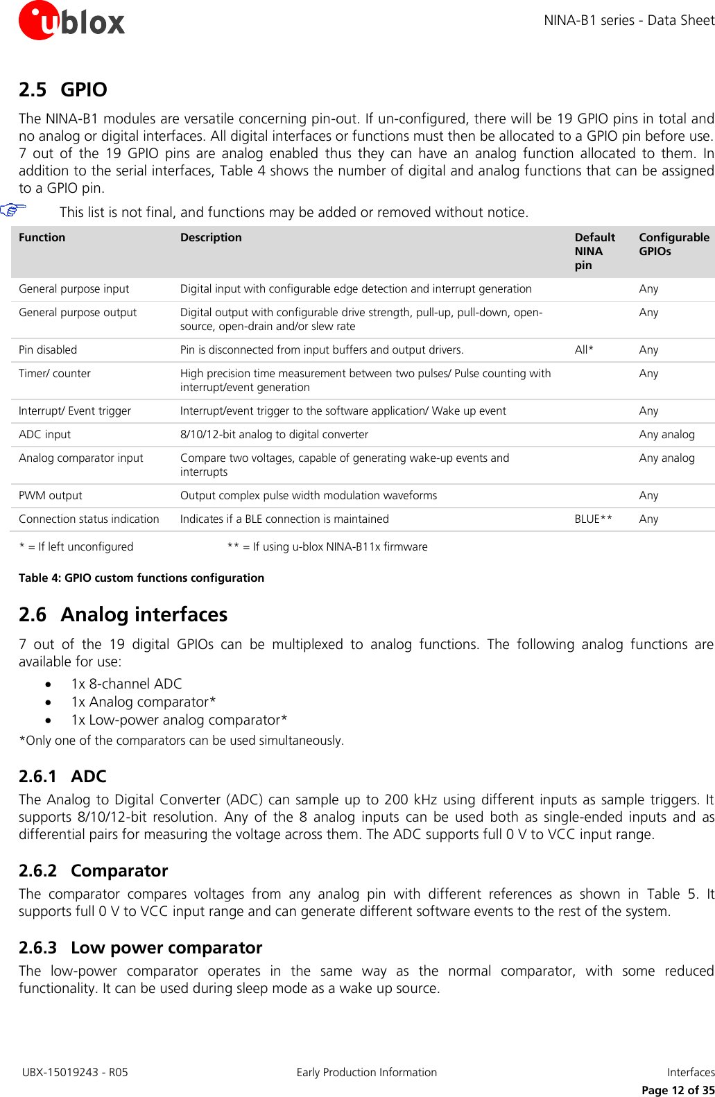
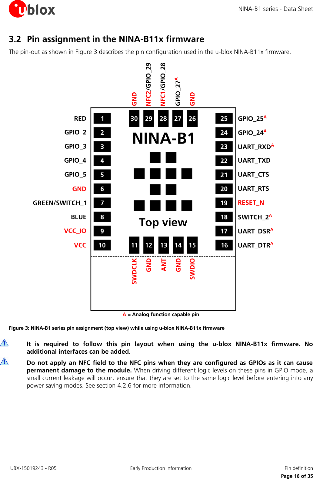
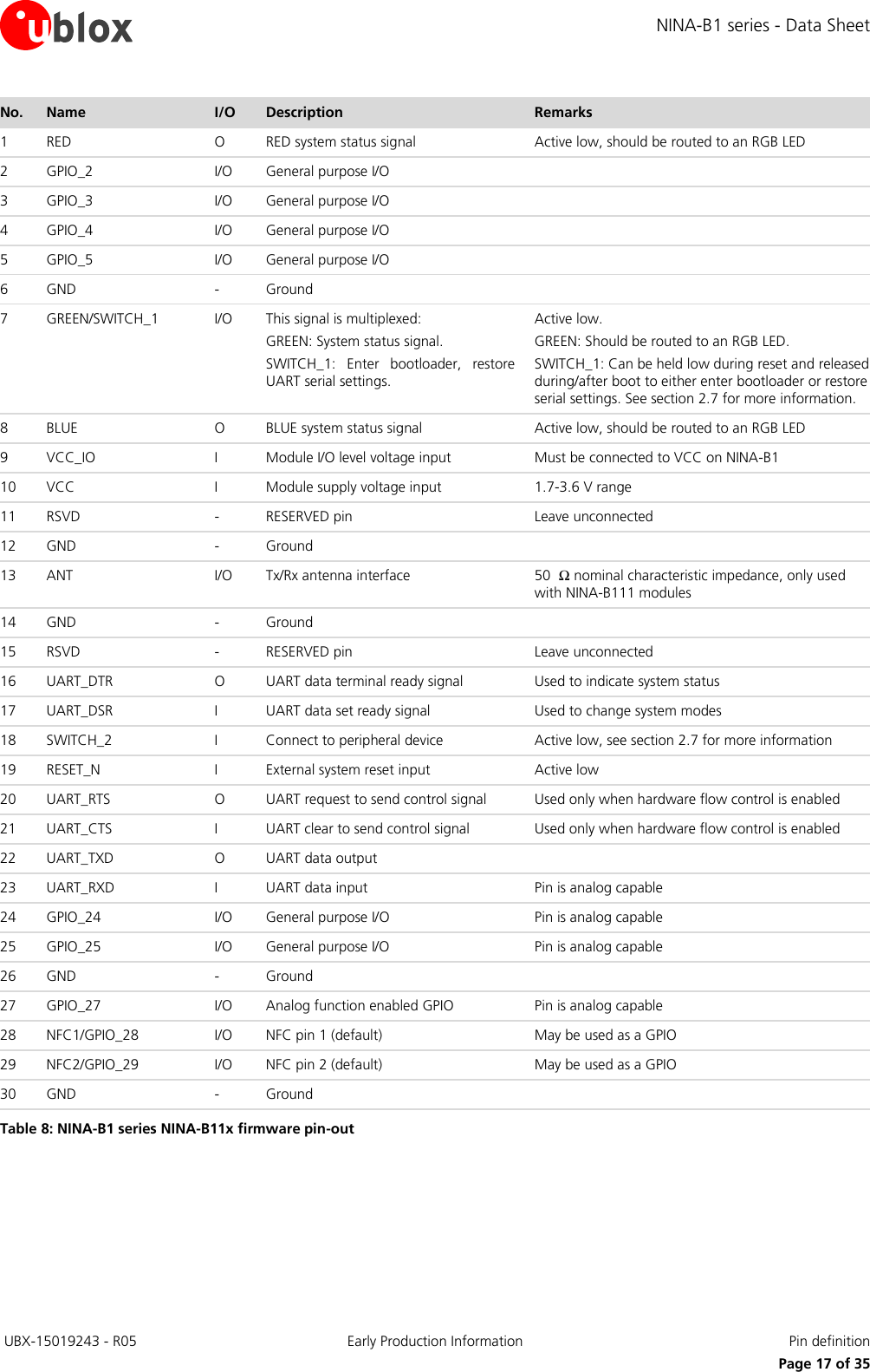
![NINA-B1 series - Data Sheet UBX-15019243 - R05 Early Production Information Interfaces Page 13 of 35 2.6.4 Analog pin options Table 5 shows the supported connections of the analog functions. An analog pin may not be simultaneously connected to multiple functions. Table 5: Possible uses of analog pin 2.7 NINA-B11x firmware features This section describes the available features when using the u-blox NINA-B11x firmware. For additional information, see the u-blox Short Range AT Commands Manual [3]. 2.7.1 System status signals The RED, GREEN and BLUE pins are used to signal the system status according to Table 6. They are active low and are intended to be routed to an RGB LED. Mode Status RGB LED Color GREEN BLUE RED Data mode IDLE Green LOW HIGH HIGH Command mode IDLE Orange LOW HIGH LOW Data mode, Command mode CONNECTING* Purple HIGH LOW LOW Data mode, Command mode CONNECTED* Blue HIGH HIGH LOW * = LED flashes on data activity Table 6: System status indication 2.7.2 System control signals The following input signals can be used to control the system. RESET_N is used to reset the system, see section 2.3.5. SWITCH_1 is used to enter the bootloader or to restore the UART serial settings to their default values. SWITCH_2 can be used to open a BLE connection to a peripheral device. If both SWITCH_1 and SWITCH_2 are driven low during start up, the system will restore all settings to their factory defaults. 2.7.3 UART signals In addition to the normal RXD, TXD, CTS, and RTS signals, the NINA-B11x firmware adds the DSR and DTR pins to the UART interface. Note that they are not used as originally intended, but to control the state of the NINA module. Depending on the current configuration, the DSR can be used to: Enter command mode Disconnect and/or toggle connectable status Enable/disable the rest of the UART interface Enter/wake up from sleep mode Analog function Can be connected to ADC single-ended input Any analog pin or VCC ADC differential input Any analog pin or VCC pair Comparator IN+ Any analog pin Comparator IN- Pin 24 or 25, VCC, 1.2 V, 1.8 V, 2.4 V Low-power comparator IN+ Any analog pin Low-power comparator IN- Pin 24 or 25, 1/16 to 15/16 VCC in steps of 1/16 VCC](https://usermanual.wiki/u-blox/NINAB1/User-Guide-3113481-Page-13.png)
![NINA-B1 series - Data Sheet UBX-15019243 - R05 Early Production Information Qualification and approvals Page 22 of 35 6 Qualification and approvals 6.1 Compliance with the RoHS directive The NINA-B1 series modules comply with the "Directive 2011/65/EU of the European Parliament and the Council on the Restriction of Use of certain Hazardous Substances in Electrical and Electronic Equipment" (RoHS). No natural rubbers, hygroscopic materials, or materials containing asbestos are employed. 6.2 European Union regulatory compliance The NINA-B1 series modules conform to the product specifications listed in Table 18. See the NINA-B1 Declaration of Conformity [4] for more information. Category Standard R&TTE Directive 1999/5/EC Effective use of frequency spectrum EN 300 328 V1.9.1 EN 302 291-1 EN 302 291-2 EMC EN 301 489-1 EN 301 489-3 EN 301 489-17 Health and safety EN 60950 Medical Electrical Equipment EN 60601-1-2 Prevention (RoHS Article 4.1) EN 50581 Table 18: NINA-B1 ETSI conformity 6.3 Safety Compliance In order to fulfill the safety standard EN 60950-1, the NINA-B1 series modules must be supplied with a Class-2 Limited Power Source. 6.4 FCC and IC Compliance 6.4.1 IC compliance This device complies with Industry Canada license-exempt RSS standard(s). Operation is subject to the following two conditions: 1. This device may not cause interference, and 2. This device must accept any interference, including interference that may cause undesired operation of the device. Under Industry Canada regulations, this radio transmitter may only operate using an antenna of a type and maximum (or lesser) gain approved for the transmitter by Industry Canada. To reduce potential radio interference to other users, the antenna type and its gain should be chosen in such a way that the equivalent isotropically radiated power (e.i.r.p.) is not more than that is necessary for successful communication. This equipment complies with IC RSS-102 radiation exposure limits set forth for an uncontrolled environment. This equipment should be installed and operated with a minimum distance of 20 cm between the radiator and your body. 6.4.2 Conformité aux norms d´IC Cet appareil est conforme à la(aux) norme(s) RSS sans licence d’Industry Canada.](https://usermanual.wiki/u-blox/NINAB1/User-Guide-3113481-Page-22.png)
![NINA-B1 series - Data Sheet UBX-15019243 - R05 Early Production Information Qualification and approvals Page 23 of 35 Son utilisation est soumise aux deux conditions suivantes: 1. Cet appareil ne doit pas causer d’interférences et 2. il doit accepter toutes interférences reçues, y compris celles susceptibles d’avoir des effets indésirables sur son fonctionnement. Conformément aux réglementations d’Industry Canada, cet émetteur radio ne peut fonctionner qu’à l’aide d’une antenne dont le type et le gain maximal (ou minimal) ont été approuvés pour cet émetteur par Industry Canada. Pour réduire le risque d’interférences avec d’autres utilisateurs, il faut choisir le type d’antenne et son gain de telle sorte que la puissance isotrope rayonnée équivalente (p.i.r.e) ne soit pas supérieure à celle requise pour obtenir une communication satisfaisante. Cet équipement respecte les limites d’exposition aux rayonnements IC RSS-102 définies pour un environnement non contrôlé. Il doit être installé et utilisé en maintenant une distance minimum de 20 cm entre le radiateur et votre corps. 6.4.3 FCC statement This device complies with Part 15 of the FCC Rules. Operation is subject to the following two conditions: 1. This device may not cause harmful interference, and 2. This device must accept any interference received, including interference that may cause undesired operation. This equipment has been tested and found to comply with the limits for a Class B digital device, pursuant to Part 15 of the FCC Rules. These limits are designed to provide reasonable protection against harmful interference in a residential installation. This equipment generates, uses and can radiate radio frequency energy and, if not installed and used in accordance with the instructions, may cause harmful interference to radio communications. However, there is no guarantee that the interference will not occur in a particular installation. If this equipment does cause harmful interference to radio or television reception, which can be determined by turning the equipment off and on, the user is encouraged to try to correct the interference by one or more of the following measures: Reorient or relocate the receiving antenna Increase the separation between the equipment and receiver Connect the equipment into an outlet on a circuit different from that to which the receiver is connected. Consult the dealer or an experienced radio/TV technician for help. The NINA-B1 series modules are for OEM integrations only. The end-user product will be professionally installed in such a manner that only the authorized antennas are used. For NINA-B111 an external antenna connector (U.FL. connector) reference design (see the NINA-B1 series System Integration Manual [1]) is available and must be followed to comply with the NINA-B1 FCC/IC modular approval. Any changes or modifications NOT explicitly APPROVED by u-blox could cause the module to cease to comply with FCC rules part 15, and thus void the user's authority to operate the equipment. 6.4.3.1 Cautions Any changes or modifications could cause the module to cease to comply with FCC rules part 15 and thus void the user's authority to operate the equipment. §15.407 statement; in case of absence of information to transmit or operational failure, the NINA-B1 module will automatically discontinue transmission.](https://usermanual.wiki/u-blox/NINAB1/User-Guide-3113481-Page-23.png)
![NINA-B1 series - Data Sheet UBX-15019243 - R05 Early Production Information Antennas Page 26 of 35 7 Antennas This chapter gives an overview of the different external antennas that can be used together with the module. This radio transmitter IC: 8595A-NINAB1 has been approved by Industry Canada to operate with the antenna types listed below with the maximum permissible gain and required antenna impedance for each antenna type indicated. Antenna types not included in this list, having a gain greater than the maximum gain indicated for that type, are strictly prohibited for use with this device. Cet émetteur radio IC: 8595A-NINAB1 été approuvé par Industry Canada pour fonctionner avec les types d’antenne énumérés ci-dessous avec le gain maximum autorisé et l’impédance nécessaire pour chaque type d’antenne indiqué. Les types d’antenne ne figurant pas dans cette liste et ayant un gain supérieur au gain maximum indiqué pour ce type-là sont strictement interdits d’utilisation avec cet appareil. 7.1 Approved antennas list # Antenna name Manufacturer Comment Gain [dBi] 1 u-blox internal antenna ProAnt SMD PIFA antenna on NINA-B112 +3 2 FlatWhip-2400 ProAnt Monopole, SMA/RSMA +3 3 InSide-2400 ProAnt Patch, 10cm cable/U.FL +3 4 Ex-IT 2400 -SMA 28-001 -RP-SMA 28-001 -MHF 28-001 ProAnt Monopole, SMA RSMA 10 cm cable/U.FL +3](https://usermanual.wiki/u-blox/NINAB1/User-Guide-3113481-Page-26.png)
![NINA-B1 series - Data Sheet UBX-15019243 - R05 Early Production Information Page 27 of 35 # Antenna name Manufacturer Comment Gain [dBi] 5 Ex-IT 2400 -SMA 70-002 -RP-SMA 70-002 ProAnt Monopole, SMA RSMA +3 6 GW26.0111.HT Taoglas Single-band monopole antenna +3 Table 21: List of antennas that are approved for use with NINA-B1](https://usermanual.wiki/u-blox/NINAB1/User-Guide-3113481-Page-27.png)
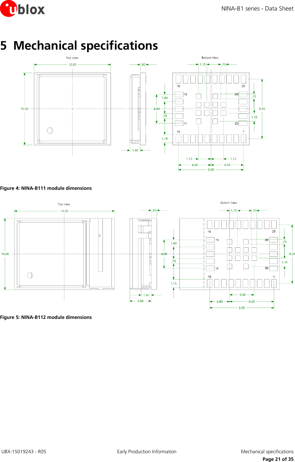
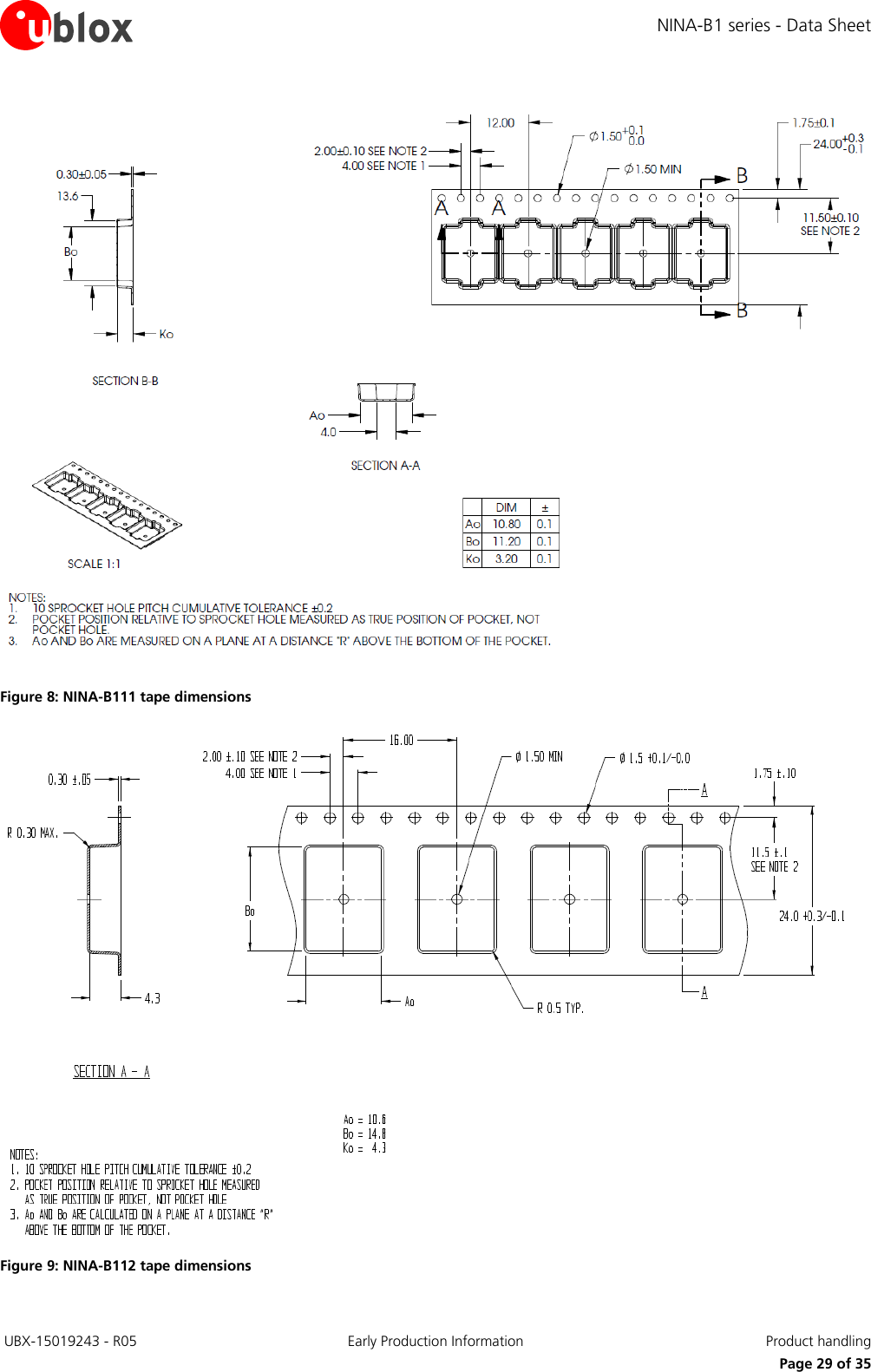
![NINA-B1 series - Data Sheet UBX-15019243 - R05 Early Production Information Product handling Page 28 of 35 8 Product handling 8.1 Packaging The NINA-B1 series modules are delivered as hermetically sealed, reeled tapes to enable efficient production, production lot set-up and tear-down. For more information about packaging, see the u-blox Package Information Guide [2]. 8.1.1 Reels NINA-B1 modules are deliverable in quantities of 500 pieces on a reel. The reel types for the NINA-B1 modules are provided in Table 22 and detailed information about the reel types are described in u-blox Package Information Guide [2]. Model Reel Type NINA-B111 B NINA-B112 A Table 22: Reel types for different models of the NINA-B1 series 8.1.2 Tapes Figure 6 and Figure 7 shows the position and orientation of the NINA-B1 modules as they are delivered on tape. The dimensions of the tapes are specified in Figure 8 and Figure 9. Figure 6: Orientation of NINA-B111 modules on tape Figure 7: Orientation of NINA-B112 modules on tape Feed direction Feed direction](https://usermanual.wiki/u-blox/NINAB1/User-Guide-3113481-Page-28.png)
![NINA-B1 series - Data Sheet UBX-15019243 - R05 Early Production Information Product handling Page 30 of 35 8.2 Moisture sensitivity levels The NINA-B1 series modules are Moisture Sensitive Devices (MSD) in accordance with the IPC/JEDEC specification. The Moisture Sensitivity Level (MSL) relates to the required packaging and handling precautions. The NINA-B1 series modules are rated at MSL level 4. For more information regarding moisture sensitivity levels, labeling and storage, see the u-blox Package Information Guide [2]. For MSL standards, see IPC/JEDEC J-STD-020, which can be downloaded from www.jedec.org. 8.3 Reflow soldering Reflow profiles are to be selected according to u-blox recommendations. See NINA-B1 series System Integration Manual [1] for more information. Failure to observe these recommendations can result in severe damage to the device. 8.4 ESD precautions The NINA-B1 series modules contain highly sensitive electronic circuitry and are Electrostatic Sensitive Devices (ESD). Handling the NINA-B1 series modules without proper ESD protection may destroy or damage them permanently. The NINA-B1 series modules are electrostatic sensitive devices (ESD) and require special ESD precautions typically applied to ESD sensitive components. Section 4.1.1 provides the maximum ESD ratings of the NINA-B1 series modules. Proper ESD handling and packaging procedures must be applied throughout the processing, handling and operation of any application that incorporates the NINA-B1 series module. The ESD precautions should be implemented on the application board where the module is mounted as described in the NINA-B1 series System Integration Manual [1]. Failure to observe these recommendations can result in severe damage to the device.](https://usermanual.wiki/u-blox/NINAB1/User-Guide-3113481-Page-30.png)
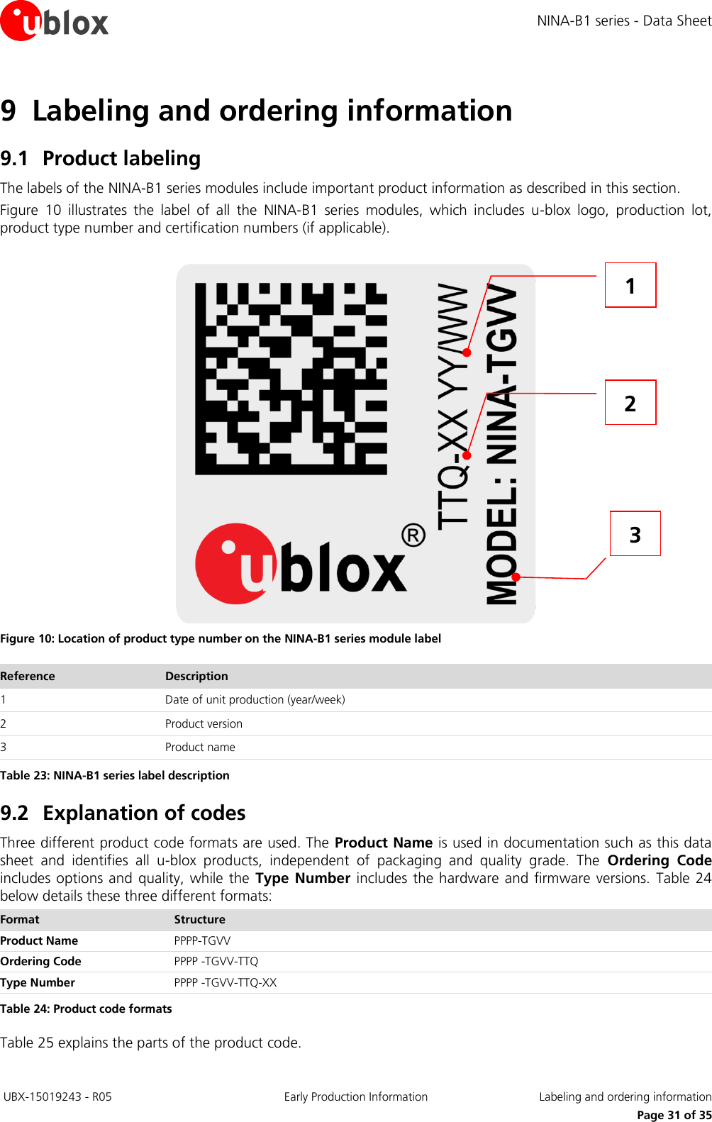
![NINA-B1 series - Data Sheet UBX-15019243 - R05 Early Production Information Labeling and ordering information Page 32 of 35 Code Meaning Example PPPP Form factor NINA TG Platform (Technology and Generation) T – Dominant technology, For example, W: Wi-Fi, B: Bluetooth G - Generation B1: Bluetooth Generation 1 VV Variant based on the same platform; range [00…99] 11: default mounting, with antenna pin TT Major Product Version 00: first revision Q Quality grade A: Automotive B: Professional C: Standard B: professional grade XX Minor product version (not relevant for certification) Default value is 00 Table 25: Part identification code 9.3 Ordering information Ordering Code Product NINA-B111-00B NINA-B1 module with antenna pin NINA-B112-00B NINA-B1 module with internal antenna Table 26: Product ordering codes](https://usermanual.wiki/u-blox/NINAB1/User-Guide-3113481-Page-32.png)
![NINA-B1 series - Data Sheet UBX-15019243 - R05 Early Production Information Related documents Page 34 of 35 Related documents [1] NINA-B1 Series System Integration Manual, document number UBX-15026175 [2] u-blox Package Information Guide, document number UBX-14001652 [3] u-blox Short Range AT Commands Manual, document number UBX-14044127 [4] NINA-B1 Declaration of Conformity, document number UBX-XXXXXX For regular updates to u-blox documentation and to receive product change notifications, register on our homepage (http://www.u-blox.com). Revision history Revision Date Name Status / Comments R01 5-Nov-2015 ajoh, fbro Initial release. R02 22-Feb-2016 ajoh In Figure 1, replaced GPIO(s) with NFC. Modified Figure 2. Added a new section for NFC (section 2.2.2) and included pin description for NFC in Table 7 and Table 8. Added Real Time Counter section (section 2.3.6). Modified sections 2.4.2, 2.5, and 2.6. Split the pin-out section into mbed/platform (section 3.1) and SPA (section 3.2) and updated these sections. Updated Figure 2. Updated NINA-B112 radio performance. Updated mechanical dimensions (section 5). Modified the number of pieces on a reel to 500 in section 8.1.1. R03 19-Apr-2016 ajoh Modified the supported Serial peripheral interface (section 2.4.2). R04 17-Jun-2016 ajoh, fbro, mhan, kgom Renamed Serial Port Application as NINA-B11x firmware. Updated the pin-out (section 3), added extra information about NFC pins and added section 2.7. Switched places of DSR and DTR pins in B11x firmware pin-out, updated system functions text (section 2.3), added measurements to electrical specifications (section 4), and a few minor changes. Included figures for tape orientation and tape dimensions in section 8.1.2. Added approved antennas list (Table 21). Document status changed to Advance Information. R05 09-Aug-2016 ajoh Updated Sections 6 and 7, document status changed to Early Production Information.](https://usermanual.wiki/u-blox/NINAB1/User-Guide-3113481-Page-34.png)