u blox NINAB22 Wireless Communication System Module User Manual NINA B2 series
u-blox AG Wireless Communication System Module NINA B2 series
UserManual.wiki
>
u blox
>
NINAB22 User Manual
Integration Manual
Navigation menu
Upload a User Manual
Namespaces
Wiki Guide
HTML
PDF
Info
Views
User Manual
Discussion / Help
Navigation
![NINA-B2 series - Data Sheet UBX-18006649 - R01 Functional description Page 6 of 41 1.4 Block diagram Figure 1: Block diagram of NINA-B2 series 1.5 Product variants The NINA-B2 series modules come with pre-flashed application software, supporting Bluetooth BR/EDR and Bluetooth low energy v4.2. The host system can set up and control the module through the AT command interface. See u-blox Short Range AT Commands Manual [3] for more information about AT commands. 1.5.1 NINA-B221 The NINA-B221 modules do not use the internal antenna and thus the PCB outline has been trimmed to 10.0 x 10.6 mm. Instead of an internal antenna, the RF signal is available at a module pin for routing to an external antenna or antenna connector. 1.5.2 NINA-B222 The NINA-B222 modules use an integrated antenna mounted on the PCB (10.0 x 14.0 mm). The RF signal pin is not connected to any signal path. Flash (16Mbit) Linear voltage regulators RF ROM IO Buffers 2xXtensa 32-bit LX6 MCU SRAM (4Mbit) Cryptographics hardware accelerations Antenna (NINA-B222) PLL Quad SPI VCC_IO VCC (3.0- 3.6V) 40 MHz Reset UART LPO (32.768 kHz, 0.7V) EFUSE * Planned feature and not supported in Software 1.0 GPIO BPF ANT (NINA-B221) Bluetooth baseband](https://usermanual.wiki/u-blox/NINAB22/User-Guide-3854277-Page-6.png)
![NINA-B2 series - Data Sheet UBX-18006649 - R01 Functional description Page 7 of 41 1.6 Radio performance The NINA-B221 and NINA-B222 modules support Bluetooth BR/EDR and Bluetooth low energy as explained in Table 2. Bluetooth BR/EDR Bluetooth low energy Bluetooth v4.2+EDR Maximum number of slaves: 7 Bluetooth 4.2 BLE dual-mode Band support 2.4 GHz, 79 channels Band support 2.4 GHz, 40 channels Maximum conducted output power 5 dBm Maximum conducted output power 5 dBm Maximum radiated output power 8 dBm EIRP* Maximum radiated output power 8 dBm EIRP* Conducted sensitivity -90 dBm Conducted sensitivity -90 dBm Data rates: 1 / 2 / 3 Mbit/s Data rates: 1 Mbit/s * RF power including maximum antenna gain (3 dBi). Table 2: NINA-B2 series Bluetooth characteristics 1.7 Software options The NINA-B2 series modules come with the pre-flashed application software, supporting Bluetooth BR/EDR and Bluetooth low energy. The host system can set up and control the module through the AT command interface. The NINA-B2 modules provide top grade security, thanks to secure boot, which ensures the module boots up only with original u-blox software. This makes NINA-B2 ideal for critical IoT applications where security is important. 1.7.1 AT command support You can configure the NINA-B221 and NINA-B222 modules with the u-blox s-center toolbox software using AT commands. See u-blox Short Range AT Commands Manual [3] for information about supported AT commands. The s-center evaluation software supporting the AT commands is also available free of charge and can be downloaded from the u-blox website. 1.7.2 Software upgrade Information on how to upgrade the software for NINA-B2 series is provided in section 2.6.2 and in the NINA-B2 series System Integration Manual [1].](https://usermanual.wiki/u-blox/NINAB22/User-Guide-3854277-Page-7.png)
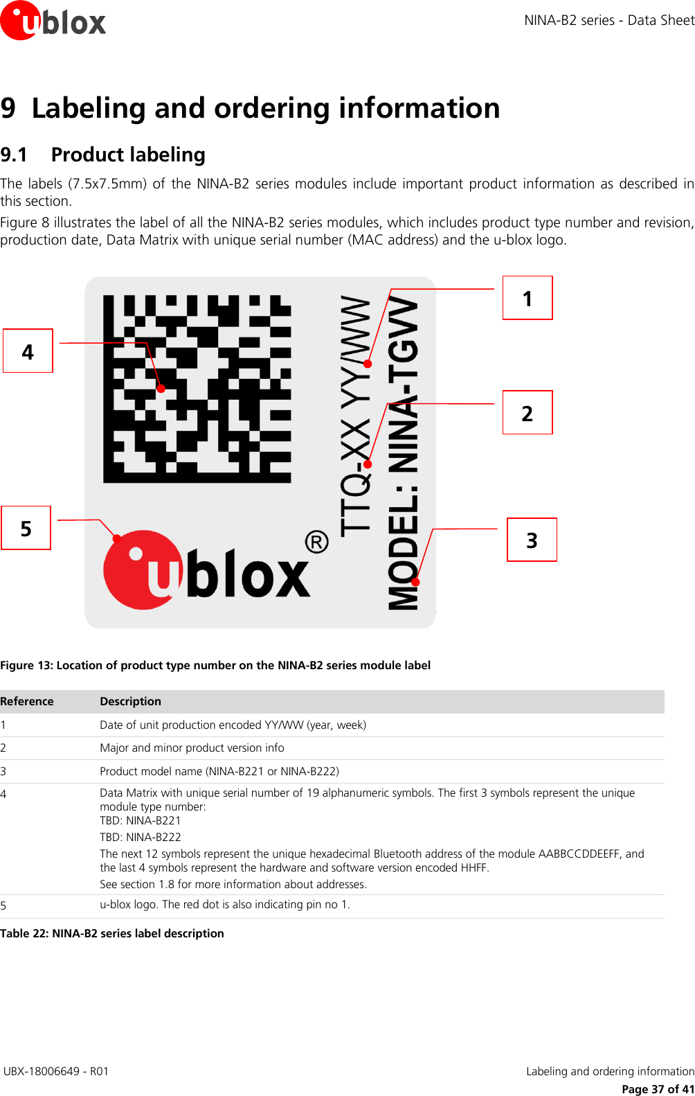
![NINA-B2 series - Data Sheet UBX-18006649 - R01 Functional description Page 8 of 41 1.8 MAC addresses The NINA-B2 module series has four unique consecutive MAC addresses reserved for each module and the addresses are stored in the configuration memory during production. The first Bluetooth address is available in the Data Matrix on the label (see section 9.1). MAC address Assignment Last bits of MAC address Example Module 1, address 1 Bluetooth 00 D4:CA:6E:90:04:90 Module 1, address 2 Reserved 01 D4:CA:6E:90:04:91 Module 1, address 3 Reserved 10 D4:CA:6E:90:04:92 Module 1, address 4 Reserved 11 D4:CA:6E:90:04:93 Module 2, address 1 Bluetooth 00 D4:CA:6E:90:04:94 Module 2, address 2 Reserved 01 D4:CA:6E:90:04:95 Module 2, address 3 Reserved 10 D4:CA:6E:90:04:96 Module 2, address 4 Reserved 11 D4:CA:6E:90:04:97 Table 3: Example MAC addresses assignment for two modules 1.9 Power modes The NINA-B2 series modules are power efficient devices capable of operating in different power saving modes and configurations. Different sections of the module can be powered off when not needed and complex wake up events can be generated from different external and internal inputs. For the lowest current consumption modes, an external LPO clock is required (see section 2.2). See the u-blox Short Range AT Commands Manual [3] and NINA-B2 series System Integration Manual [1] for more information about power modes.](https://usermanual.wiki/u-blox/NINAB22/User-Guide-3854277-Page-8.png)
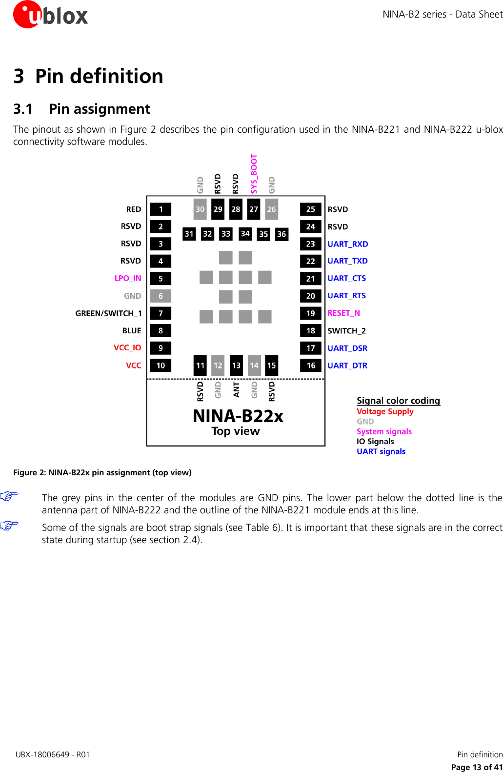
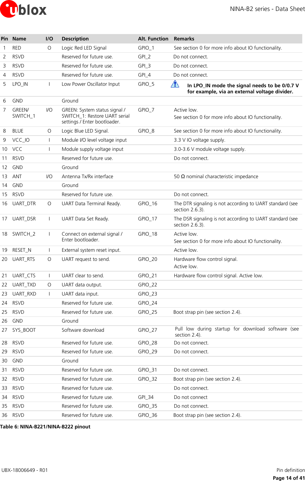
![NINA-B2 series - Data Sheet UBX-18006649 - R01 Interfaces Page 9 of 41 2 Interfaces 2.1 Power supply The power for NINA-B2 series modules is supplied through VCC and VCC_IO pins by DC voltage. The system power supply circuit must be able to support peak power (add 20% as margin over the listed type current consumption), as during operation, the current drawn from VCC and VCC_IO can vary significantly based on the use cases. 2.1.1 Module supply input (VCC) The NINA-B2 series modules use an integrated Linear Voltage converter to transform the supply voltage presented at the VCC pin into a stable system voltage. 2.1.2 Digital I/O interfaces reference voltage (VCC_IO) All modules in the NINA-B2 series provide an additional voltage supply input for setting the I/O voltage level. The separate VCC_IO pin enables integration of the module in many applications with different voltage levels (for example, 1.8 V or 3.3 V) without any level converters. The NINA-B2 modules support only 3.3 V as IO voltage level currently. 2.2 Low Power Clock The NINA-B2 series module does not have an internal low power oscillator (LPO), which is required for low power modes. An external 32.768 KHz LPO signal can be supplied externally via the LPO_CLK pin if low power modes are required. The low power clock voltage level is lower (0/0.7 V) compared to the digital signal levels and a voltage divider can be required (see section 4.2.4). 2.3 Module reset The NINA-B2 series modules can be reset (rebooted) in one of the following ways: Low level on the RESET_N pin, which is normally set high by an internal pull-up. This causes “hardware” reset of the module. The RESET_N signal should be driven by an open drain, open collector or contact switch. When RESET_N is low (off), the chip works at the minimum power. The NINA-B2 series modules can be reset using an AT command (see the u-blox Short Range AT Commands Manual [3]). This causes a “software” reset of the module. 2.4 Boot strapping pins There are several boot configuration pins available on the module that needs to have the correct settings during boot. It is important that they are in the default state (marked with bold in Table 4) during startup for normal operation. The default state is automatically selected (with internal pull-ups or pull-downs) if the pins are left unconnected. Pin State during boot Default Behavior Description 36 0 VDD_SDIO=3.3V Voltage of Internal Flash 1 10 kΩ pull-up VDD_SDIO=1.8V (VDD_SDIO should always be 1.8 V) 27, 25 00 Download Boot Booting Mode, see section 1.7 for information about 01 Reserved, do not use](https://usermanual.wiki/u-blox/NINAB22/User-Guide-3854277-Page-9.png)
![NINA-B2 series - Data Sheet UBX-18006649 - R01 Interfaces Page 10 of 41 Pin State during boot Default Behavior Description 10 Pull-up*, Pull-down* Normal Boot from internal Flash software upgrade. 11 Normal Boot from internal Flash 32 0 Silent Debugging Log on U0TXD during booting 1 Pull-up* U0TXD Toggling 32, 28 00 Falling-edge input, falling-edge output Timing of SDIO Slave 01 Falling-edge input, rising-edge output 10 Rising-edge input, falling-edge output 11 Pull-up*, Pull-up* Rising-edge input, rising-edge output * About 30 kΩ Table 4: NINA-B2 series boot strapping pins 2.5 RF antenna interface The RF antenna interface of the NINA-B2 series supports Bluetooth BR/EDR and Bluetooth low energy on the same RF antenna signal. The module is equipped with a 2.4 GHz bandpass filter between the radio chip and RF antenna interface (see section 1.4). The NINA-B2 series supports either an internal antenna (NINA-B222) or external antennas connected through an antenna pin (NINA-B221). 2.5.1 Internal antenna The NINA-B222 module has an internal (embedded) 2.4 GHz PIFA antenna. The internal antenna is a PIFA antenna specifically designed and optimized for the NINA form factor. Keep a minimum clearance of 5 mm between the antenna and the casing. Keep a minimum of 10 mm free space from the metal around the antenna including the area below. If a metal enclosure is required, use NINA-B221 and an external antenna. It is recommended to place the NINA-B222 modules in such a way that the internal antenna is in the corner of the host PCB (the corner closest to Pin 16 should be in the corner). The antenna side (short side closest to the antenna), positioned along one side of the host PCB ground plane is the second best option. It is beneficial to have a large solid ground plane on the host PCB and have a good grounding on the NINA-B222 module. Minimum ground plane size is 24x30 mm but recommended is more than 50x50 mm. See NINA-B2 series System Integration Manual [1] for more information about antenna related design. The ANT signal is not available on the solder pins of the NINA-B222 module. 2.5.2 External RF antenna interface The NINA-B221 module has an antenna signal (ANT) pin with a characteristic impedance of 50 Ω for using an external antenna. The antenna signal supports both Tx and Rx. The external antenna, for example, can be an SMD antenna (or PCB integrated antenna) on the host board. An antenna connector for using an external antenna via a coaxial cable could also be implemented. A cable antenna might be necessary if the module is mounted in a shielded enclosure such as a metal box or cabinet. An external antenna connector (U.FL. connector) reference design (see NINA-B2 series System Integration Manual [1]) is available and must be followed to comply with the NINA-B2 FCC/IC modular approvals. Also see the list of approved antennas (section 7.2).](https://usermanual.wiki/u-blox/NINAB22/User-Guide-3854277-Page-10.png)
![NINA-B2 series - Data Sheet UBX-18006649 - R01 Interfaces Page 11 of 41 2.6 IO signals 2.6.1 System status IO signals The RED, GREEN and BLUE pins are used to signal the status. They are active low and are intended to be routed to an RGB LED. See u-blox Short Range AT Commands Manual [3] for more information about connectivity software signals IOs. Mode Status RGB LED Color GREEN BLUE RED Data mode IDLE Green LOW HIGH HIGH Command mode IDLE Orange LOW HIGH LOW Data mode, Command mode CONNECTING* Purple HIGH LOW LOW Data mode, Command mode CONNECTED* Blue HIGH HIGH LOW * = LED flashes on data activity Table 5: System status indication 2.6.2 System control IO signals The following input signals are used to control the system (see u-blox Short Range AT Commands Manual [3] for more information about connectivity software signals IOs): RESET_N is used to reset the system. See section 0 for detailed information. If SWITCH_2 is driven low during start up, the UART serial settings are restored to their default values. SWITCH_2 can be used to open a connection to a peripheral device. If both SWITCH_1 and SWITCH_2 are driven low during start up, the system will enter the bootloader mode. If both SWITCH_1 and SWITCH_2 are driven low during start up and held low for 10 seconds, the system will exit the bootloader mode and restore all settings to their factory defaults. 2.6.3 UART IO signals In addition to the normal RXD, TXD, CTS, and RTS signals, the NINA-B221/NINA-B222 software adds the DSR and DTR pins to the UART interface. Note that they are not used as originally intended, but to control the state of the NINA module. Depending on the current configuration, the DSR pin can be used to: Enter command mode. Disconnect and/or toggle connectable status. Enable/disable the rest of the UART interface. Enter/wake up from sleep mode. 2.7 Data interfaces 2.7.1 UART The NINA-B221 and NINA-B222 modules include a 6-wire UART for communication with an application host processor (AT commands, Data communication, and software upgrades). The following UART signals are available: Data lines (RXD as input, TXD as output) Hardware flow control lines (CTS as input, RTS as output) Link status (DTR as output, DSR as input). The DTR/DSR signals behavior is adapted to the u-blox connectivity software functionality and differs from the UART standard, see section 2.6.3 for additional information. Programmable baud-rate generator allows most industry standard rates, as well as non-standard rates up to 921600 bps.](https://usermanual.wiki/u-blox/NINAB22/User-Guide-3854277-Page-11.png)
![NINA-B2 series - Data Sheet UBX-18006649 - R01 Mechanical specifications Page 19 of 41 5 Mechanical specifications 5.1 NINA-B221 Mechanical specification Figure 3: NINA-B221 mechanical outline Parameter Description Typical Tolerance A Module PCB Length [mm] 10.6 (417.3 mil) +0.20/-0.10 (+7.9/-3.9 mil) B Module PCB Width [mm] 10.0 (393.7 mil) +0.20/-0.10 (+7.9/-3.9 mil) C Module Thickness [mm] 2.2 (86.6 mil) +0.40/-0.20 (+15.8/-7.9 mil) ccc Seating Plane Coplanarity [mm] 0.10 (3.9 mil) +0.02/-0.10 (+0.8/-3.9 mil) D Horizontal Edge to Lateral Pin No 1 Edge [mm] 0.45 (17.7 mil) +0.10/-0.10 (+3.9/-3.9 mil) E Vertical and Horizontal Edge to Lateral Pin No 1 Edge [mm] 0.30 (11.8 mil) +0.10/-0.10 (+3.9/-3.9 mil) F Vertical Pin No1 Edge to Lateral Pin Edge [mm] 2.35 (92.5 mil) +0.05/-0.05 (+2.0/-2.0 mil) G Depanalizing Residual [mm] 0.10 (3.9 mil) +0.25/-0.10 (+9.8/-3.9 mil) H Lateral and Antenna Row Pin to Pin Pitch [mm] 1.0 (39.4 mil) +0.05/-0.05 (+2.0/-2.0 mil) I Lateral and Antenna Row Pin Width [mm] 0.70 (27.6 mil) +0.05/-0.05 (+2.0/-2.0 mil) J Lateral and Antenna Row Pin Height [mm] 1.15 (45.3 mil) +0.05/-0.05 (+2.0/-2.0 mil) K Horizontal Pin No1 Edge to Central Pin Edge [mm] 2.78 (109.4 mil) +0.05/-0.05 (+2.0/-2.0 mil) L Vertical Pin No1 Edge to Central Pin Edge [mm] 2.63 (103.5 mil) +0.05/-0.05 (+2.0/-2.0 mil) M Horizontal Pin No1 Edge to Inner Row Pin Edge [mm] 1.45 (57.1 mil) +0.05/-0.05 (+2.0/-2.0 mil) N Vertical Pin No1 Edge to Inner Row Pin Edge [mm] 1.6 (63.0 mil) +0.05/-0.05 (+2.0/-2.0 mil) O Central Pin and Inner Row Width and Height [mm] 0.70 (27.6 mil) +0.05/-0.05 (+2.0/-2.0 mil) P Central Pin to Central Pin Pitch [mm] 1.15 (45.3 mil) +0.05/-0.05 (+2.0/-2.0 mil) Q Inner Row Pin to Pin Pitch [mm] 1.1 (43.3 mil) +0.05/-0.05 (+2.0/-2.0 mil) R Horizontal Pin No1 Edge to Antenna Row Pin Edge [mm] 8.7 (342.5 mil) +0.05/-0.05 (+2.0/-2.0 mil) Module Weight [g] <1.0 Table 17: NINA-B221 mechanical outline data](https://usermanual.wiki/u-blox/NINAB22/User-Guide-3854277-Page-19.png)
![NINA-B2 series - Data Sheet UBX-18006649 - R01 Mechanical specifications Page 20 of 41 5.2 NINA-B222 Mechanical specification Figure 4: NINA-B222 mechanical outline Parameter Description Typical Tolerance A Module PCB Length [mm] 14.0 (551.2 mil) +0.20/-0.10 (+7.9/-3.9 mil) B Module PCB Width [mm] 10.0 (393.7 mil) +0.20/-0.10 (+7.9/-3.9 mil) C Module Thickness [mm] 3.8 (149.6 mil) +0.40/-0.20 (+15.8/-7.9 mil) ccc Seating Plane Coplanarity [mm] 0.10 (3.9 mil) +0.02/-0.10 (+0.8/-3.9 mil) D Horizontal Edge to Lateral Pin No 1 Edge [mm] 0.45 (17.7 mil) +0.10/-0.10 (+3.9/-3.9 mil) E Vertical and Horizontal Edge to Lateral Pin No 1 Edge [mm] 0.30 (11.8 mil) +0.10/-0.10 (+3.9/-3.9 mil) F Vertical Pin No1 Edge to Lateral Pin Edge [mm] 2.35 (92.5 mil) +0.05/-0.05 (+2.0/-2.0 mil) G Depanalizing Residual [mm] 0.10 (3.9 mil) +0.25/-0.10 (+9.8/-3.9 mil) H Lateral and Antenna Row Pin to Pin Pitch [mm] 1.0 (39.4 mil) +0.05/-0.05 (+2.0/-2.0 mil) I Lateral and Antenna Row Pin Width [mm] 0.70 (27.6 mil) +0.05/-0.05 (+2.0/-2.0 mil) J Lateral and Antenna Row Pin Height [mm] 1.15 (45.3 mil) +0.05/-0.05 (+2.0/-2.0 mil) K Horizontal Pin No1 Edge to Central Pin Edge [mm] 2.78 (109.4 mil) +0.05/-0.05 (+2.0/-2.0 mil) L Vertical Pin No1 Edge to Central Pin Edge [mm] 2.63 (103.5 mil) +0.05/-0.05 (+2.0/-2.0 mil) M Horizontal Pin No1 Edge to Inner Row Pin Edge [mm] 1.45 (57.1 mil) +0.05/-0.05 (+2.0/-2.0 mil) N Vertical Pin No1 Edge to Inner Row Pin Edge [mm] 1.6 (63.0 mil) +0.05/-0.05 (+2.0/-2.0 mil) O Central Pin and Inner Row Width and Height [mm] 0.70 (27.6 mil) +0.05/-0.05 (+2.0/-2.0 mil) P Central Pin to Central Pin Pitch [mm] 1.15 (45.3 mil) +0.05/-0.05 (+2.0/-2.0 mil) Q Inner Row Pin to Pin Pitch [mm] 1.1 (43.3 mil) +0.05/-0.05 (+2.0/-2.0 mil) R Horizontal Pin No1 Edge to Antenna Row Pin Edge [mm] 8.7 (342.5 mil) +0.05/-0.05 (+2.0/-2.0 mil) S PCB and Shield Cover Thickness [mm] 2.2 (86.6 mil) +0.40/-0.20 (+15.8/-7.9 mil) T Module Antenna Width [mm] 3.8 (149.6 mil) +0.20/-0.20 (+7.9/-7.9 mil) U Antenna overhang outside module outline on any side [mm] 0.0 (0.0 mil) +0.60 (+23.6 mil) Module Weight [g] <1.0 Table 18: NINA-B222 mechanical outline data](https://usermanual.wiki/u-blox/NINAB22/User-Guide-3854277-Page-20.png)
![NINA-B2 series - Data Sheet UBX-18006649 - R01 Qualification and approvals Page 22 of 41 6.3.1.1 FCC Compliance The NINA-B2 modules are for OEM integrations only. The end product must be professionally installed in such manner that only the authorized antennas can be used. For NINA-B221, an external antenna connector (U.FL. connector) reference design is available and must be followed to comply with the NINA-B2 FCC/IC modular approval (see the NINA-B2 series System Integration Manual [1]). 6.3.1.2 FCC statement This device complies with Part 15 of the FCC Rules. Operation is subject to the following two conditions: 1. This device may not cause harmful interference, and 2. This device must accept any interference received, including interference that may cause undesired operation. This equipment has been tested and found to comply with the limits for a Class B digital device, pursuant to Part 15 of the FCC Rules. These limits are designed to provide reasonable protection against harmful interference in a residential installation. This equipment generates, uses and can radiate radio frequency energy and, if not installed and used in accordance with the instructions, may cause harmful interference to radio communications. However, there is no guarantee that the interference will not occur in a particular installation. If this equipment does cause harmful interference to radio or television reception, which can be determined by turning the equipment off and on, the user is encouraged to try to correct the interference by one or more of the following measures: Reorient or relocate the receiving antenna Increase the separation between the equipment and receiver Connect the equipment into an outlet on a circuit different from that to which the receiver is connected. Consult the dealer or an experienced radio/TV technician for help. 6.3.2 RF-exposure statement 6.3.2.1 IC Compliance This equipment complies with the requirements of IC RSS-102 issue 5 radiation exposure limits set forth for an uncontrolled environment. Having a separation distance of minimum 30 mm between the user and/or bystander and the antenna and /or radiating element ensures that the output power (e.i.r.p.) of NINA-B221 and NINA-B222 is below the SAR evaluation Exemption limits defined in RSS-102 issue 5. 6.3.2.2 FCC Compliance This device complies with the FCC radiation exposure limits set forth for an uncontrolled environment. Having a separation distance of minimum 25 mm between the user and/or bystander and the antenna and /or radiating element ensures that maximum output power of NINA-B221 and NINA-B222 is below the SAR test exclusion limits presented in KDB 447498 D01v06.](https://usermanual.wiki/u-blox/NINAB22/User-Guide-3854277-Page-22.png)
![NINA-B2 series - Data Sheet UBX-18006649 - R01 Qualification and approvals Page 25 of 41 6.4 Japan radio equipment compliance Approvals are pending. The Japan certification is pending and the information in this section will be applicable when the module Japan certification is completed. TBD Figure 6: Giteki mark, R and the NINA-B2 MIC certification number For information about compliance of the NINA-B2 module with the Giteki certification, see the NINA-B2 Series System Integration Manual [1].](https://usermanual.wiki/u-blox/NINAB22/User-Guide-3854277-Page-25.png)
![NINA-B2 series - Data Sheet UBX-18006649 - R01 Qualification and approvals Page 27 of 41 6.6 Safety compliance In order to fulfill the safety standard EN 60950-1, the NINA-B2 series modules must be supplied with a Class-2 Limited Power Source. 6.7 Bluetooth qualification information Approvals are pending. The Bluetooth qualification is pending and the information in this section will be applicable when the qualification is completed. The NINA-B221/NINA-B222 modules have been qualified as a controller subsystem according to the Bluetooth 4.2 specification. Figure 7: Bluetooth logo indicating Bluetooth Qualification Product type QD ID Listing Date Controller Subsystem 107058 14-Mar-2018 Host Subsystem TBD TBD End Product TBD TBD Table 20: NINA-B221/NINA-B222 Bluetooth QD ID For information on how to list and declare your product, see the NINA-B2 Series System Integration Manual [1].](https://usermanual.wiki/u-blox/NINAB22/User-Guide-3854277-Page-27.png)
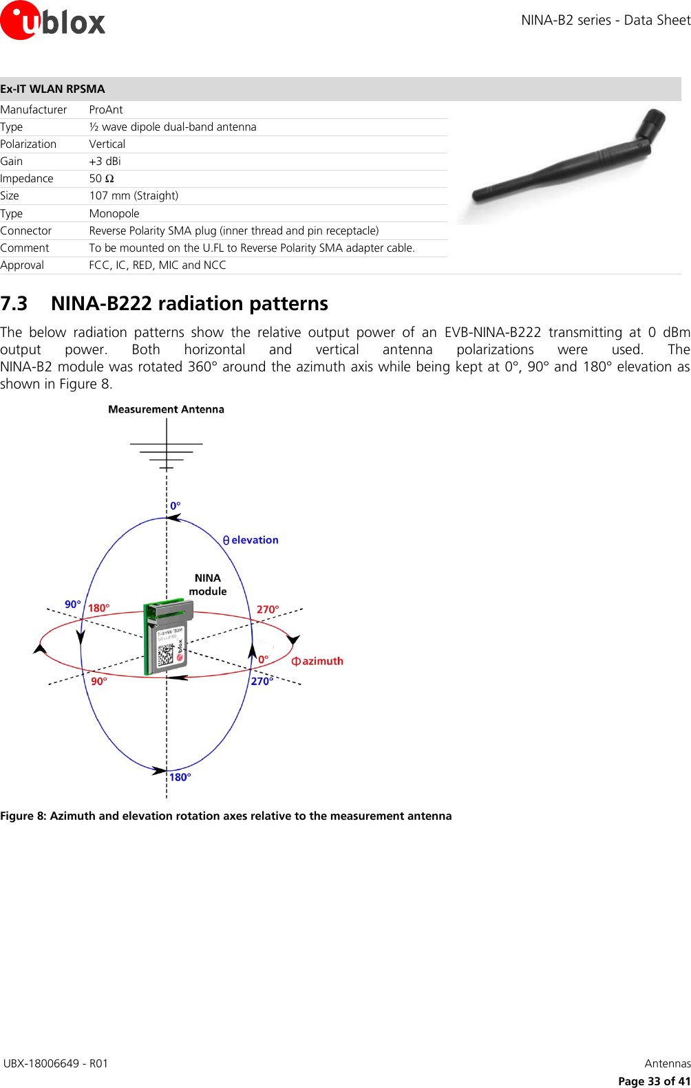
![NINA-B2 series - Data Sheet UBX-18006649 - R01 Antennas Page 28 of 41 7 Antennas This chapter gives an overview of the different external antennas that can be used together with the module. This radio transmitter IC: 8595A-NINAB22 has been approved by Industry Canada to operate with the antenna types listed below with the maximum permissible gain and required antenna impedance for each antenna type indicated. Antenna types not included in this list, having a gain greater than the maximum gain indicated for that type, are strictly prohibited for use with this device. Cet émetteur radio IC: 8595A-NINAB22 été approuvé par Industry Canada pour fonctionner avec les types d’antenne énumérés ci-dessous avec le gain maximum autorisé et l’impédance nécessaire pour chaque type d’antenne indiqué. Les types d’antenne ne figurant pas dans cette liste et ayant un gain supérieur au gain maximum indiqué pour ce type-là sont strictement interdits d’utilisation avec cet appareil. For each antenna, the "Approvals" field defines in which test reports the antenna is included. Definitions of the «Approvals» field are: FCC - The antenna is included in the FCC test reports and thus approved for use in countries that accept the FCC radio approvals, primarily US. IC - The antenna is included in the IC (Industrie Canada) test reports and thus approved for use in countries that accept the IC radio approvals, primarily Canada. RED - The antenna is included in the ETSI test reports and thus approved for use in countries that accept the Radio Equipment Directive, primarily the European countries. MIC - The antenna is included in the Japanese government affiliated MIC test reports and thus approved for use in the Japanese market. NCC - The antenna is included in the Taiwan NCC test reports and thus approved for use in Taiwan. In general, antennas with SMD connection, Reverse Polarity SMA connector or U.FL connector are included in FCC, IC, RED, NCC and MIC radio tests. The antennas with SMA connector are included in RED, NCC and MIC radio tests but not in the FCC or IC due to FCC/IC regulations. The external antennas are connected to the board through U.FL connectors. Some antennas are connected directly to the U.FL connector of the board while some are connected using an SMA or reversed polarity SMA connector through a short U.FL to SMA or reversed polarity SMA adapter cable. 7.1 Antenna accessories Name U.FL to SMA adapter cable Connector U.FL and SMA jack (outer thread and pin receptacle) Impedance 50 Ω Minimum cable loss 0.5 dB, The cable loss must be above the minimum cable loss to meet the regulatory requirements. Minimum cable length 100 mm. Comment The SMA connector can be mounted in a panel. See NINA-B2 series System Integration Manual [1] for information how to integrate the U.FL connector. Approval RED, MIC and NCC](https://usermanual.wiki/u-blox/NINAB22/User-Guide-3854277-Page-28.png)
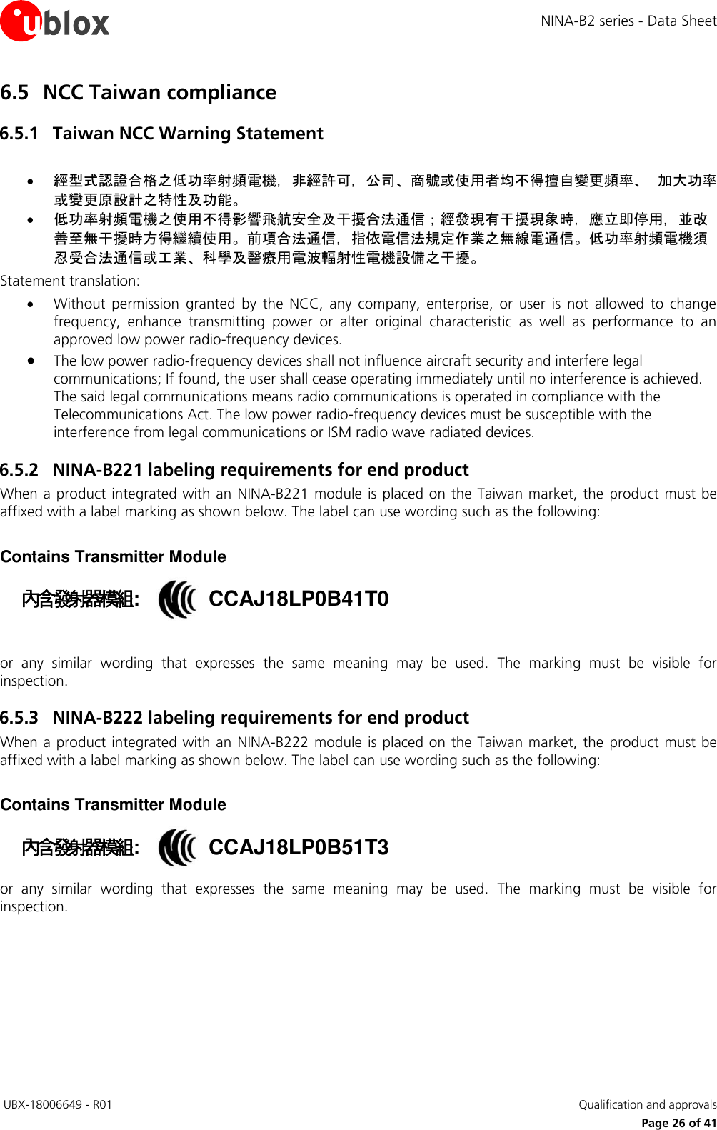
![NINA-B2 series - Data Sheet UBX-18006649 - R01 Antennas Page 29 of 41 Name U.FL to Reverse Polarity SMA adapter cable Connector U.FL and Reverse Polarity SMA jack (outer thread and pin) Impedance 50 Ω Minimum cable loss 0.5 dB, The cable loss must be above the minimum cable loss to meet the regulatory requirements. Minimum cable length 100 mm. Comment The Reverse Polarity SMA connector can be mounted in a panel. See NINA-B2 series System Integration Manual [1] for information how to integrate the U.FL connector. It is required to followed this reference design to comply with the NINA-B22 FCC/IC modular approvals. Approval FCC, IC, RED, MIC and NCC 7.2 Approved antennas 7.2.1 Single band antennas NINA-B222 Manufacturer ProAnt Gain +3 dBi Impedance 50 Ω Size (HxWxL) 3.0 x 3.8 x 9.9 mm Type PIFA Comment SMD PIFA antenna on NINA-B222. Should not be mounted inside a metal enclosure, see section for more info 2.5.1. Approval FCC, IC, RED, MIC and NCC GW.26.0111 Manufacturer Taoglas Polarization Vertical Gain +2.0 dBi Impedance 50 Ω Size Ø 7.9 x 30.0 mm Type Monopole Connector SMA (M) . Comment To be mounted on the U.FL to SMA adapter cable. Approval FCC, IC, RED, MIC, and NCC ANT-2.4-CW-RH-RPS Manufacturer Linx Polarization Vertical Gain -1.0 dBi Impedance 50 Ω Size Ø 7.4 x 27.0 mm Type Monopole Connector Reverse Polarity SMA plug (inner thread and pin receptacle). Comment To be mounted on the U.FL to Reverse Polarity SMA adapter cable. An SMA version antenna is also available but not recommended for use (ANT-2.4-CW-RH-SMA). Approval FCC, IC, RED, MIC and NCC](https://usermanual.wiki/u-blox/NINAB22/User-Guide-3854277-Page-29.png)
![NINA-B2 series - Data Sheet UBX-18006649 - R01 Antennas Page 30 of 41 Ex-IT 2400 RP-SMA 28-001 Manufacturer ProAnt Polarization Vertical Gain +3.0 dBi Impedance 50 Ω Size Ø 12.0 x 28.0 mm Type Monopole Connector Reverse Polarity SMA plug (inner thread and pin receptacle). Comment This antenna requires to be mounted on a metal ground plane for best performance. To be mounted on the U.FL to Reverse Polarity SMA adapter cable. An SMA version antenna is also available but not recommended for use (Ex-IT 2400 SMA 28-001). Approval FCC, IC, RED, MIC and NCC Ex-IT 2400 MHF 28 Manufacturer ProAnt Polarization Vertical Gain +2.0 dBi Impedance 50 Ω Size Ø 12.0 x 28.0 mm Type Monopole Cable length 100 mm Connector U.FL. connector Comment This antenna requires to be mounted on a metal ground plane for best performance. To be mounted on a U.FL connector. See NINA-B2 series System Integration Manual [1] for information how to integrate the U.FL connector. It is required to followed this reference design to comply with the NINA -W13 FCC/IC modular approvals. Approval FCC, IC, RED, MIC and NCC Ex-IT 2400 RP-SMA 70-002 Manufacturer ProAnt Polarization Vertical Gain +3.0 dBi Impedance 50 Ω Size Ø 10 x 83 mm Type Monopole Connector Reverse Polarity SMA plug (inner thread and pin receptacle) Comment To be mounted on the U.FL to Reverse Polarity SMA adapter cable. An SMA version antenna is also available but not recommended for use (Ex-IT 2400 SMA 70-002). Approval FCC, IC, RED, MIC and NCC](https://usermanual.wiki/u-blox/NINAB22/User-Guide-3854277-Page-30.png)
![NINA-B2 series - Data Sheet UBX-18006649 - R01 Antennas Page 31 of 41 Ex-IT 2400 MHF 70-001 Manufacturer ProAnt Polarization Vertical Gain +3.0 dBi Impedance 50 Ω Size Ø 9.4 x 70.5 mm Type Monopole Cable length 100 mm Connector U.FL. connector Comment To be mounted on a U.FL connector. See NINA-B2 series System Integration Manual [1] for information how to integrate the U.FL connector. It is required to followed this reference design to comply with the NINA-B2 FCC/IC modular approvals. Approval FCC, IC, RED, MIC and NCC InSide-2400 Manufacturer ProAnt Gain +3.0 dBi Impedance 50 Ω Size 27 x 12 mm (triangular) Type Patch Cable length 100 mm Connector U.FL. connector Comment Should be attached to a plastic enclosure or part for best performance. To be mounted on a U.FL connector. See NINA-B2 series System Integration Manual [1] for information how to integrate the U.FL connector. It is required to followed this reference design to comply with the NINA-B2 FCC/IC modular approvals. Approval FCC, IC, RED, MIC and NCC FlatWhip-2400 Manufacturer ProAnt Gain +3.0 dBi Impedance 50 Ω Size Ø 50.0 x 30.0 mm Type Monopole Connector SMA plug (inner thread and pin) Comment To be mounted on the U.FL to SMA adapter cable. Approval RED, MIC and NCC](https://usermanual.wiki/u-blox/NINAB22/User-Guide-3854277-Page-31.png)
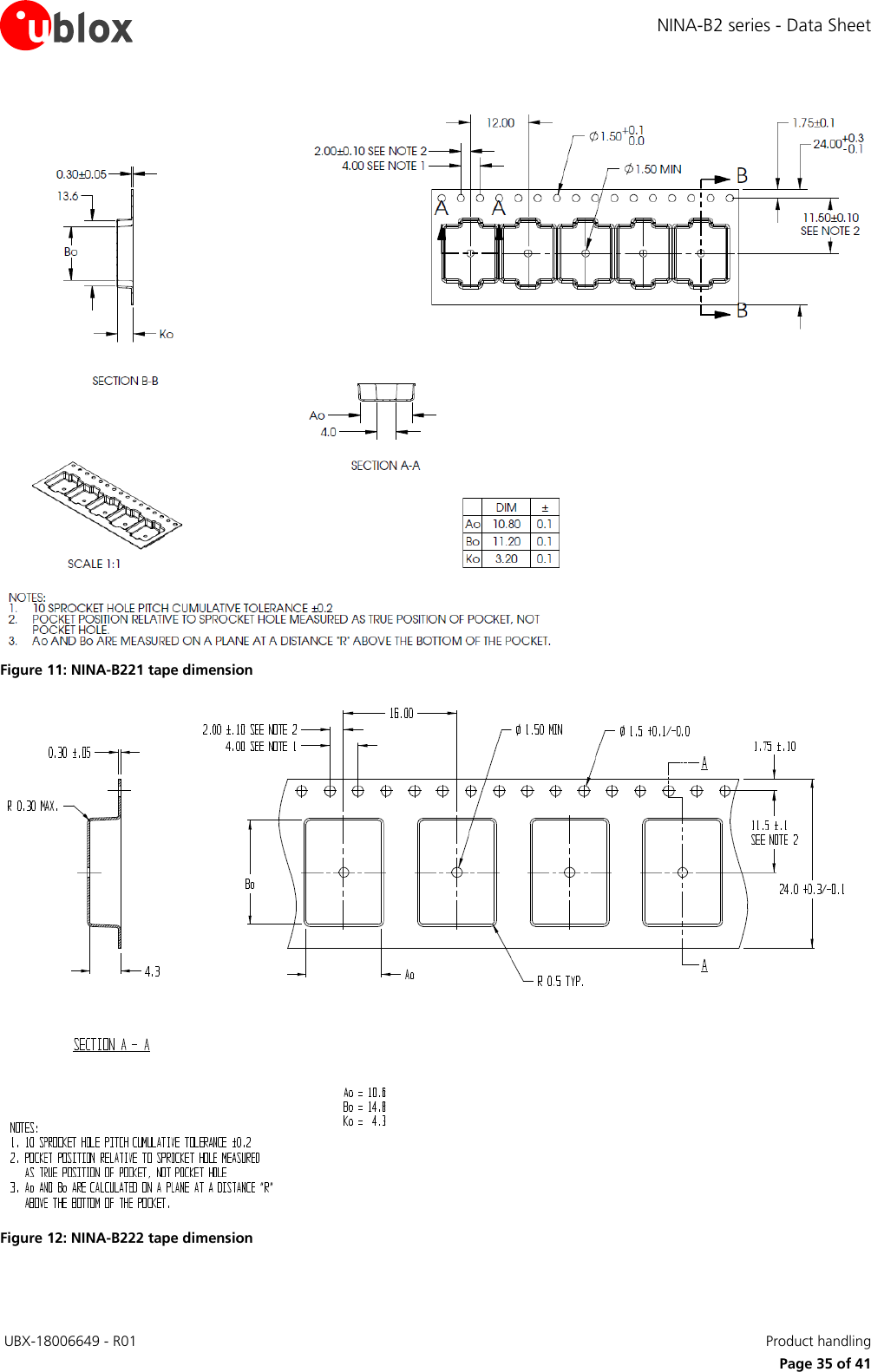
![NINA-B2 series - Data Sheet UBX-18006649 - R01 Antennas Page 32 of 41 Outside-2400 Manufacturer ProAnt Gain +3.0 dBi Impedance 50 Ω Size 36.0 x 18.0 x 16.0 mm Type Patch Cable length 70 mm Connector U.FL. connector Comment To be mounted on a U.FL connector. See NINA-B2 series System Integration Manual [1] for information how to integrate the U.FL connector. It is required to followed this reference design to comply with the NINA-B2 FCC/IC modular approvals. Approval FCC, IC, RED, MIC and NCC 7.2.2 Dual-band antennas InSide-WLAN Manufacturer ProAnt Gain +3.0 dBi Impedance 50 Ω Size 27 x 12 mm (triangular) Type Patch Cable length 100 mm Connector U.FL. connector Comment Should be attached to a plastic enclosure or part for best performance. Dual-band (2.4 GHz / 5 GHz) antenna to be mounted on a U.FL connector. See NINA-B2 series System Integration Manual [1] for information how to integrate the U.FL connector. It is required to followed this reference design to comply with the NINA-B2 FCC/IC modular approvals. Approval FCC, IC, RED, MIC and NCC InSide-WLAN Square Manufacturer ProAnt Gain +3.0 dBi Impedance 50 Ω Size 24x22x1 mm with mounting hole Type Patch Cable length 100 mm Connector U.FL. connector Comment Should be attached to a plastic enclosure or part for best performance. Dual-band (2.4 GHz / 5 GHz) antenna to be mounted on a U.FL connector. See NINA-B2 series System Integration Manual [1] for information on how to integrate the U.FL connector. It is required to followed this reference design to comply with the NINA-B2 FCC/IC modular approvals. Approval FCC, IC, RED, MIC and NCC](https://usermanual.wiki/u-blox/NINAB22/User-Guide-3854277-Page-32.png)
![NINA-B2 series - Data Sheet UBX-18006649 - R01 Product handling Page 34 of 41 8 Product handling 8.1 Packaging The NINA-B2 series modules are in development status as mentioned in the table on page 2. Hence, the information in this section will be applicable only when the module is fully tested and approved in the Initial Production stage. 8.1.1 Reels The NINA-B2 series modules are delivered as hermetically sealed, reeled tapes to enable efficient production, production lot set-up and tear-down. For more information about packaging, see the u-blox Package Information Guide [2]. NINA-B2 modules are deliverable in quantities of 500 pieces on a reel. The reel types for the NINA-B2 modules are provided in Table 21 and detailed information about the reel types are described in u-blox Package Information Guide [2]. Model Reel Type NINA-B221 B NINA-B222 A Table 21: Reel types for the different models of NINA-B2 series 8.1.2 Tapes Figure 9 and Figure 10 shows the position and orientation of the NINA-B2 modules as they are delivered on tape. The dimensions of the tapes are specified in Figure 11 and Figure 12. Figure 9: Orientation of NINA-B221 module on tape Figure 10: Orientation of NINA-B222 module on tape Feed direction Feed direction](https://usermanual.wiki/u-blox/NINAB22/User-Guide-3854277-Page-34.png)
![NINA-B2 series - Data Sheet UBX-18006649 - R01 Product handling Page 36 of 41 8.2 Moisture sensitivity levels The NINA-B2 series modules are Moisture Sensitive Devices (MSD) in accordance with the IPC/JEDEC specification. The Moisture Sensitivity Level (MSL) relates to the required packaging and handling precautions. The NINA-B2 series modules are rated at MSL level 4. For more information regarding moisture sensitivity levels, labeling and storage, see the u-blox Package Information Guide [2]. For MSL standards, see IPC/JEDEC J-STD-020, which can be downloaded from www.jedec.org. 8.3 Reflow soldering Reflow profiles are to be selected according to u-blox recommendations. See NINA-B2 series System Integration Manual [1] for more information. Failure to observe these recommendations can result in severe damage to the device. 8.4 ESD precautions The NINA-B2 series modules contain highly sensitive electronic circuitry and are Electrostatic Sensitive Devices (ESD). Handling the NINA-B2 series modules without proper ESD protection may destroy or damage them permanently. The NINA-B2 series modules are electrostatic sensitive devices (ESD) and require special ESD precautions typically applied to ESD sensitive components. Section 4.1.1 provides the maximum ESD ratings of the NINA-B2 series modules. Proper ESD handling and packaging procedures must be applied throughout the processing, handling and operation of any application that incorporates the NINA-B2 series module. The ESD precautions should be implemented on the application board where the module is mounted as described in the NINA-B2 series System Integration Manual [1]. Failure to observe these recommendations can result in severe damage to the device.](https://usermanual.wiki/u-blox/NINAB22/User-Guide-3854277-Page-36.png)
![NINA-B2 series - Data Sheet UBX-18006649 - R01 Labeling and ordering information Page 38 of 41 9.2 Explanation of codes Three different product code formats are used. The Product Name is used in documentation such as this data sheet and identifies all u-blox products, independent of packaging and quality grade. The Ordering Code includes options and quality, while the Type Number includes the hardware and software versions. Table 23 below details these three different formats: Format Structure Product Name PPPP-TGVV Ordering Code PPPP -TGVV-TTQ Type Number PPPP -TGVV-TTQ-XX Table 23: Product code formats Table 24 explains the parts of the product code. Code Meaning Example PPPP Form factor NINA TG Platform (Technology and Generation) T – Dominant technology, For example, W: Wi-Fi, B: Bluetooth G - Generation B2: Bluetooth Generation 2 VV Variant based on the same platform; range [00…99] 21: u-blox connectivity software product with antenna pin TT Major Product Version 00: first revision Q Quality grade A: Automotive B: Professional C: Standard B: professional grade XX Minor product version (not relevant for certification) Default value is 00 Table 24: Part identification code 9.3 Ordering information Ordering Code Product NINA-B221-00B-00 Bluetooth dual-mode module with antenna pin. With u-blox connectivity software including secure boot. NINA-B222-00B-00 Bluetooth dual-mode module module with internal onboard antenna. With u-blox connectivity software including secure boot. Table 25: Product ordering codes](https://usermanual.wiki/u-blox/NINAB22/User-Guide-3854277-Page-38.png)
![NINA-B2 series - Data Sheet UBX-18006649 - R01 Related documents Page 40 of 41 Related documents [1] NINA-B2 Series System Integration Manual, UBX-18011096 [2] u-blox Package Information Guide, document number UBX-14001652 [3] u-blox Short Range AT Commands Manual, document number UBX-14044127 For regular updates to u-blox documentation and to receive product change notifications, register on our homepage (http://www.u-blox.com).](https://usermanual.wiki/u-blox/NINAB22/User-Guide-3854277-Page-40.png)