u blox NINAB22 Wireless Communication System Module User Manual NINA B2 series
u-blox AG Wireless Communication System Module NINA B2 series
u blox >
Integration Manual
NINA-B2 series
Stand-alone Bluetooth dual-mode
modules
Data Sheet
www.u-blox.com
UBX-18006649 - R01
Abstract
This technical data sheet describes the NINA-B2 series stand-alone
Bluetooth® dual-mode modules. The NINA-B2 modules come with
pre-flashed application software, Bluetooth dual-mode (Bluetooth
BR/EDR and Bluetooth low energy). The module has a number of
important security features embedded, including secure boot, which
ensures that only authenticated software can run on the module.
This makes NINA-B2 ideal for critical IoT applications where security
is important.
NINA-B2 series - Data Sheet
UBX-18006649 - R01 Functional description
Page 2 of 41
Document Information
Title
NINA-B2 series
Subtitle
Stand-alone Bluetooth dual-mode modules
Document type
Data Sheet
Document number
UBX-18006649
Revision and date
R01
16-Mar-2018
Disclosure restriction
Product Status
Corresponding content status
Functional Sample
Draft
For functional testing. Revised and supplementary data will be published later.
In Development /
Prototype
Objective Specification
Target values. Revised and supplementary data will be published later.
Engineering Sample
Advance Information
Data based on early testing. Revised and supplementary data will be published later.
Initial Production
Early Prod. Information
Data from product verification. Revised and supplementary data may be published later.
Mass Production /
End of Life
Production Information
Final product specification.
This document applies to the following products:
Product name
Type number
u-blox connectivity software version
PCN reference
Product status
NINA-B221
NINA-B221-00B-00
1.0.0
N/A
In Development
NINA-B222
NINA-B222-00B-00
1.0.0
N/A
In Development
u-blox reserves all rights to this document and the information contained herein. Products, names, logos and designs described herein may in
whole or in part be subject to intellectual property rights. Reproduction, use, modification or disclosure to third parties of this document or
any part thereof without the express permission of u-blox is strictly prohibited.
The information contained herein is provided “as is” and u-blox assumes no liability for the use of the information. No warranty, either
express or implied, is given, including but not limited, with respect to the accuracy, correctness, reliability and fitness for a particular purpose
of the information. This document may be revised by u-blox at any time. For most recent documents, visit www.u-blox.com.
Copyright © 2018, u-blox AG.
u-blox is a registered trademark of u-blox Holding AG in the EU and other countries. Arm is the registered trademark of Arm Limited in the
EU and other countries.

NINA-B2 series - Data Sheet
UBX-18006649 - R01 Functional description
Page 3 of 41
Contents
1 Functional description .................................................................................................. 5
1.1 Overview .............................................................................................................................................. 5
1.2 Applications .......................................................................................................................................... 5
1.3 Product features ................................................................................................................................... 5
1.4 Block diagram ....................................................................................................................................... 6
1.5 Product variants .................................................................................................................................... 6
1.5.1 NINA-B221 .................................................................................................................................... 6
1.5.2 NINA-B222 .................................................................................................................................... 6
1.6 Radio performance ............................................................................................................................... 7
1.7 Software options .................................................................................................................................. 7
1.7.1 AT command support .................................................................................................................... 7
1.7.2 Software upgrade ......................................................................................................................... 7
1.8 MAC addresses ..................................................................................................................................... 8
1.9 Power modes ........................................................................................................................................ 8
2 Interfaces ...................................................................................................................... 9
2.1 Power supply ........................................................................................................................................ 9
2.1.1 Module supply input (VCC) ........................................................................................................... 9
2.1.2 Digital I/O interfaces reference voltage (VCC_IO) ........................................................................... 9
2.2 Low Power Clock .................................................................................................................................. 9
2.3 Module reset ........................................................................................................................................ 9
2.4 Boot strapping pins............................................................................................................................... 9
2.5 RF antenna interface ........................................................................................................................... 10
2.5.1 Internal antenna .......................................................................................................................... 10
2.5.2 External RF antenna interface ...................................................................................................... 10
2.6 IO signals ............................................................................................................................................ 11
2.6.1 System status IO signals ............................................................................................................... 11
2.6.2 System control IO signals ............................................................................................................. 11
2.6.3 UART IO signals ........................................................................................................................... 11
2.7 Data interfaces ................................................................................................................................... 11
2.7.1 UART ........................................................................................................................................... 11
3 Pin definition .............................................................................................................. 13
3.1 Pin assignment ................................................................................................................................... 13
4 Electrical specifications .............................................................................................. 15
4.1 Absolute maximum ratings ................................................................................................................. 15
4.1.1 Maximum ESD ratings ................................................................................................................. 15
4.2 Operating conditions .......................................................................................................................... 15
4.2.1 Operating temperature range ...................................................................................................... 15
4.2.2 Supply/Power pins ....................................................................................................................... 16
4.2.3 RESET_N pin ................................................................................................................................ 16
4.2.4 LPO clock .................................................................................................................................... 16
4.2.5 Digital pins .................................................................................................................................. 17

NINA-B2 series - Data Sheet
UBX-18006649 - R01 Functional description
Page 4 of 41
4.2.6 Current consumption .................................................................................................................. 17
4.2.7 Bluetooth radio characteristics ..................................................................................................... 17
4.2.8 Bluetooth low energy characteristics ........................................................................................... 18
5 Mechanical specifications .......................................................................................... 19
5.1 NINA-B221 Mechanical specification ................................................................................................... 19
5.2 NINA-B222 Mechanical specification ................................................................................................... 20
6 Qualification and approvals ...................................................................................... 21
6.1 Country approvals .............................................................................................................................. 21
6.2 European Union regulatory compliance .............................................................................................. 21
6.2.1 Radio Equipment Directive (RED) 2014/53/EU .............................................................................. 21
6.2.2 Compliance with the RoHS directive ............................................................................................ 21
6.3 FCC/IC Compliance............................................................................................................................. 21
6.4 Japan radio equipment compliance ..................................................................................................... 25
6.5 NCC Taiwan compliance ..................................................................................................................... 26
6.5.1 Taiwan NCC Warning Statement ................................................................................................. 26
6.5.2 NINA-B221 labeling requirements for end product ...................................................................... 26
6.5.3 NINA-B222 labeling requirements for end product ...................................................................... 26
6.6 Safety compliance ............................................................................................................................... 27
6.7 Bluetooth qualification information .................................................................................................... 27
7 Antennas ..................................................................................................................... 28
7.1 Antenna accessories ........................................................................................................................... 28
7.2 Approved antennas ............................................................................................................................ 29
7.2.1 Single band antennas .................................................................................................................. 29
7.2.2 Dual-band antennas .................................................................................................................... 32
7.3 NINA-B222 radiation patterns ............................................................................................................. 33
8 Product handling ........................................................................................................ 34
8.1 Packaging ........................................................................................................................................... 34
8.1.1 Reels ........................................................................................................................................... 34
8.1.2 Tapes .......................................................................................................................................... 34
8.2 Moisture sensitivity levels .................................................................................................................... 36
8.3 Reflow soldering ................................................................................................................................. 36
8.4 ESD precautions .................................................................................................................................. 36
9 Labeling and ordering information ........................................................................... 37
9.1 Product labeling .................................................................................................................................. 37
9.2 Explanation of codes........................................................................................................................... 38
9.3 Ordering information .......................................................................................................................... 38
Appendix .......................................................................................................................... 39
A Glossary ...................................................................................................................... 39
Related documents........................................................................................................... 40
Contact .............................................................................................................................. 41
NINA-B2 series - Data Sheet
UBX-18006649 - R01 Functional description
Page 5 of 41
1 Functional description
1.1 Overview
The NINA-B2 series are small, stand-alone Bluetooth dual-mode modules designed for ease-of-use and
integration in professional applications. The modules are delivered with u-blox connectivity software that
provides support for both peripheral and central roles, Serial Port Profile, GATT client and server, beacons, u-blox
Bluetooth low energy Serial Port Service – all configurable from a host using AT commands.
The NINA-B2 modules provide top grade security, thanks to secure boot, which ensures the module only boots
up with original u-blox software. Intended applications include industrial automation, wireless-connected and
configurable equipment, point-of-sales, and health devices. The NINA-B2 series is globally certified for use with
the internal antenna or a range of external antennas.
1.2 Applications
Internet of Things (IoT)
Bluetooth networks
Telematics
Point-of-sales
Medical and industrial networking
Access to laptops, mobile phones, and similar consumer devices
Home/building automation
Ethernet/Wireless Gateway
1.3 Product features
Table 1: NINA-B2 series main features summary
NINA-B2 series - Data Sheet
UBX-18006649 - R01 Functional description
Page 6 of 41
1.4 Block diagram
Figure 1: Block diagram of NINA-B2 series
1.5 Product variants
The NINA-B2 series modules come with pre-flashed application software, supporting Bluetooth BR/EDR and
Bluetooth low energy v4.2. The host system can set up and control the module through the AT command
interface. See u-blox Short Range AT Commands Manual [3] for more information about AT commands.
1.5.1 NINA-B221
The NINA-B221 modules do not use the internal antenna and thus the PCB outline has been trimmed to
10.0 x 10.6 mm. Instead of an internal antenna, the RF signal is available at a module pin for routing to an
external antenna or antenna connector.
1.5.2 NINA-B222
The NINA-B222 modules use an integrated antenna mounted on the PCB (10.0 x 14.0 mm). The RF signal pin is
not connected to any signal path.
Flash (16Mbit)
Linear voltage regulators
RF
ROM
IO Buffers
2xXtensa 32-bit LX6 MCU
SRAM (4Mbit)
Cryptographics
hardware
accelerations
Antenna
(NINA-B222)
PLL
Quad SPI
VCC_IO
VCC (3.0- 3.6V)
40 MHz
Reset
UART
LPO (32.768 kHz, 0.7V)
EFUSE
* Planned feature and not supported in Software 1.0
GPIO
BPF
ANT (NINA-B221)
Bluetooth
baseband

NINA-B2 series - Data Sheet
UBX-18006649 - R01 Functional description
Page 7 of 41
1.6 Radio performance
The NINA-B221 and NINA-B222 modules support Bluetooth BR/EDR and Bluetooth low energy as explained in
Table 2.
Bluetooth BR/EDR
Bluetooth low energy
Bluetooth v4.2+EDR
Maximum number of slaves: 7
Bluetooth 4.2 BLE dual-mode
Band support
2.4 GHz, 79 channels
Band support
2.4 GHz, 40 channels
Maximum conducted output power
5 dBm
Maximum conducted output power
5 dBm
Maximum radiated output power
8 dBm EIRP*
Maximum radiated output power
8 dBm EIRP*
Conducted sensitivity
-90 dBm
Conducted sensitivity
-90 dBm
Data rates:
1 / 2 / 3 Mbit/s
Data rates:
1 Mbit/s
* RF power including maximum antenna gain (3 dBi).
Table 2: NINA-B2 series Bluetooth characteristics
1.7 Software options
The NINA-B2 series modules come with the pre-flashed application software, supporting Bluetooth BR/EDR and
Bluetooth low energy. The host system can set up and control the module through the AT command interface.
The NINA-B2 modules provide top grade security, thanks to secure boot, which ensures the module boots up
only with original u-blox software. This makes NINA-B2 ideal for critical IoT applications where security is
important.
1.7.1 AT command support
You can configure the NINA-B221 and NINA-B222 modules with the u-blox s-center toolbox software using AT
commands. See u-blox Short Range AT Commands Manual [3] for information about supported AT commands.
The s-center evaluation software supporting the AT commands is also available free of charge and can be
downloaded from the u-blox website.
1.7.2 Software upgrade
Information on how to upgrade the software for NINA-B2 series is provided in section 2.6.2 and in the NINA-B2
series System Integration Manual [1].
NINA-B2 series - Data Sheet
UBX-18006649 - R01 Functional description
Page 8 of 41
1.8 MAC addresses
The NINA-B2 module series has four unique consecutive MAC addresses reserved for each module and the
addresses are stored in the configuration memory during production. The first Bluetooth address is available in
the Data Matrix on the label (see section 9.1).
MAC address
Assignment
Last bits of MAC address
Example
Module 1, address 1
Bluetooth
00
D4:CA:6E:90:04:90
Module 1, address 2
Reserved
01
D4:CA:6E:90:04:91
Module 1, address 3
Reserved
10
D4:CA:6E:90:04:92
Module 1, address 4
Reserved
11
D4:CA:6E:90:04:93
Module 2, address 1
Bluetooth
00
D4:CA:6E:90:04:94
Module 2, address 2
Reserved
01
D4:CA:6E:90:04:95
Module 2, address 3
Reserved
10
D4:CA:6E:90:04:96
Module 2, address 4
Reserved
11
D4:CA:6E:90:04:97
Table 3: Example MAC addresses assignment for two modules
1.9 Power modes
The NINA-B2 series modules are power efficient devices capable of operating in different power saving modes
and configurations. Different sections of the module can be powered off when not needed and complex wake
up events can be generated from different external and internal inputs. For the lowest current consumption
modes, an external LPO clock is required (see section 2.2).
See the u-blox Short Range AT Commands Manual [3] and NINA-B2 series System Integration Manual [1] for
more information about power modes.

NINA-B2 series - Data Sheet
UBX-18006649 - R01 Interfaces
Page 9 of 41
2 Interfaces
2.1 Power supply
The power for NINA-B2 series modules is supplied through VCC and VCC_IO pins by DC voltage.
The system power supply circuit must be able to support peak power (add 20% as margin over the listed
type current consumption), as during operation, the current drawn from VCC and VCC_IO can vary
significantly based on the use cases.
2.1.1 Module supply input (VCC)
The NINA-B2 series modules use an integrated Linear Voltage converter to transform the supply voltage
presented at the VCC pin into a stable system voltage.
2.1.2 Digital I/O interfaces reference voltage (VCC_IO)
All modules in the NINA-B2 series provide an additional voltage supply input for setting the I/O voltage level.
The separate VCC_IO pin enables integration of the module in many applications with different voltage levels
(for example, 1.8 V or 3.3 V) without any level converters. The NINA-B2 modules support only 3.3 V as IO
voltage level currently.
2.2 Low Power Clock
The NINA-B2 series module does not have an internal low power oscillator (LPO), which is required for low
power modes. An external 32.768 KHz LPO signal can be supplied externally via the LPO_CLK pin if low power
modes are required.
The low power clock voltage level is lower (0/0.7 V) compared to the digital signal levels and a
voltage divider can be required (see section 4.2.4).
2.3 Module reset
The NINA-B2 series modules can be reset (rebooted) in one of the following ways:
Low level on the RESET_N pin, which is normally set high by an internal pull-up. This causes
“hardware” reset of the module. The RESET_N signal should be driven by an open drain, open collector
or contact switch. When RESET_N is low (off), the chip works at the minimum power.
The NINA-B2 series modules can be reset using an AT command (see the u-blox Short Range AT
Commands Manual [3]). This causes a “software” reset of the module.
2.4 Boot strapping pins
There are several boot configuration pins available on the module that needs to have the correct settings during
boot. It is important that they are in the default state (marked with bold in Table 4) during startup for normal
operation. The default state is automatically selected (with internal pull-ups or pull-downs) if the pins are left
unconnected.
Pin
State during boot
Default
Behavior
Description
36
0
VDD_SDIO=3.3V
Voltage of Internal Flash
1
10 kΩ pull-up
VDD_SDIO=1.8V
(VDD_SDIO should always be 1.8 V)
27, 25
00
Download Boot
Booting Mode, see section
1.7 for information about
01
Reserved, do not use
NINA-B2 series - Data Sheet
UBX-18006649 - R01 Interfaces
Page 10 of 41
Pin
State during boot
Default
Behavior
Description
10
Pull-up*, Pull-down*
Normal Boot from internal Flash
software upgrade.
11
Normal Boot from internal Flash
32
0
Silent
Debugging Log on U0TXD
during booting
1
Pull-up*
U0TXD Toggling
32, 28
00
Falling-edge input, falling-edge output
Timing of SDIO Slave
01
Falling-edge input, rising-edge output
10
Rising-edge input, falling-edge output
11
Pull-up*, Pull-up*
Rising-edge input, rising-edge output
* About 30 kΩ
Table 4: NINA-B2 series boot strapping pins
2.5 RF antenna interface
The RF antenna interface of the NINA-B2 series supports Bluetooth BR/EDR and Bluetooth low energy on the
same RF antenna signal. The module is equipped with a 2.4 GHz bandpass filter between the radio chip and RF
antenna interface (see section 1.4).
The NINA-B2 series supports either an internal antenna (NINA-B222) or external antennas connected through an
antenna pin (NINA-B221).
2.5.1 Internal antenna
The NINA-B222 module has an internal (embedded) 2.4 GHz PIFA antenna. The internal antenna is a PIFA
antenna specifically designed and optimized for the NINA form factor.
Keep a minimum clearance of 5 mm between the antenna and the casing. Keep a minimum of 10 mm free
space from the metal around the antenna including the area below. If a metal enclosure is required, use
NINA-B221 and an external antenna.
It is recommended to place the NINA-B222 modules in such a way that the internal antenna is in the corner of
the host PCB (the corner closest to Pin 16 should be in the corner). The antenna side (short side closest to the
antenna), positioned along one side of the host PCB ground plane is the second best option. It is beneficial to
have a large solid ground plane on the host PCB and have a good grounding on the NINA-B222 module.
Minimum ground plane size is 24x30 mm but recommended is more than 50x50 mm.
See NINA-B2 series System Integration Manual [1] for more information about antenna related design.
The ANT signal is not available on the solder pins of the NINA-B222 module.
2.5.2 External RF antenna interface
The NINA-B221 module has an antenna signal (ANT) pin with a characteristic impedance of 50 Ω for using an
external antenna. The antenna signal supports both Tx and Rx.
The external antenna, for example, can be an SMD antenna (or PCB integrated antenna) on the host board. An
antenna connector for using an external antenna via a coaxial cable could also be implemented. A cable antenna
might be necessary if the module is mounted in a shielded enclosure such as a metal box or cabinet.
An external antenna connector (U.FL. connector) reference design (see NINA-B2 series System Integration
Manual [1]) is available and must be followed to comply with the NINA-B2 FCC/IC modular approvals.
Also see the list of approved antennas (section 7.2).

NINA-B2 series - Data Sheet
UBX-18006649 - R01 Interfaces
Page 11 of 41
2.6 IO signals
2.6.1 System status IO signals
The RED, GREEN and BLUE pins are used to signal the status. They are active low and are intended to be routed
to an RGB LED. See u-blox Short Range AT Commands Manual [3] for more information about connectivity
software signals IOs.
Mode
Status
RGB LED Color
GREEN
BLUE
RED
Data mode
IDLE
Green
LOW
HIGH
HIGH
Command mode
IDLE
Orange
LOW
HIGH
LOW
Data mode, Command mode
CONNECTING*
Purple
HIGH
LOW
LOW
Data mode, Command mode
CONNECTED*
Blue
HIGH
HIGH
LOW
* = LED flashes on data activity
Table 5: System status indication
2.6.2 System control IO signals
The following input signals are used to control the system (see u-blox Short Range AT Commands Manual [3] for
more information about connectivity software signals IOs):
RESET_N is used to reset the system. See section 0 for detailed information.
If SWITCH_2 is driven low during start up, the UART serial settings are restored to their default values.
SWITCH_2 can be used to open a connection to a peripheral device.
If both SWITCH_1 and SWITCH_2 are driven low during start up, the system will enter the bootloader
mode.
If both SWITCH_1 and SWITCH_2 are driven low during start up and held low for 10 seconds, the
system will exit the bootloader mode and restore all settings to their factory defaults.
2.6.3 UART IO signals
In addition to the normal RXD, TXD, CTS, and RTS signals, the NINA-B221/NINA-B222 software adds the DSR
and DTR pins to the UART interface. Note that they are not used as originally intended, but to control the state
of the NINA module. Depending on the current configuration, the DSR pin can be used to:
Enter command mode.
Disconnect and/or toggle connectable status.
Enable/disable the rest of the UART interface.
Enter/wake up from sleep mode.
2.7 Data interfaces
2.7.1 UART
The NINA-B221 and NINA-B222 modules include a 6-wire UART for communication with an application host
processor (AT commands, Data communication, and software upgrades).
The following UART signals are available:
Data lines (RXD as input, TXD as output)
Hardware flow control lines (CTS as input, RTS as output)
Link status (DTR as output, DSR as input). The DTR/DSR signals behavior is adapted to the u-blox
connectivity software functionality and differs from the UART standard, see section 2.6.3 for additional
information.
Programmable baud-rate generator allows most industry standard rates, as well as non-standard rates
up to 921600 bps.

NINA-B2 series - Data Sheet
UBX-18006649 - R01 Interfaces
Page 12 of 41
Frame format configuration:
o 8 data bits
o Even or no-parity bit
o 1 stop bit
Default frame configuration is 8N1, meaning eight (8) data bits, no (N) parity bit, and one (1) stop bit.
NINA-B2 series - Data Sheet
UBX-18006649 - R01 Pin definition
Page 13 of 41
3 Pin definition
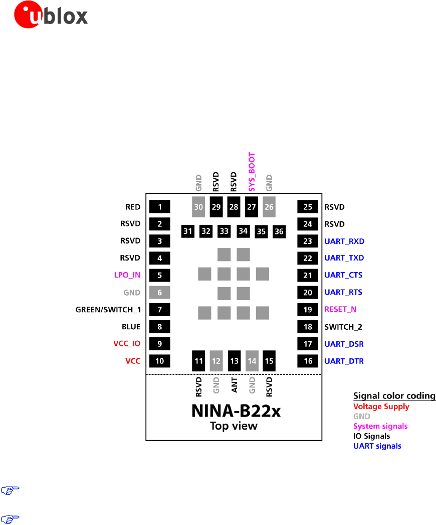
3.1 Pin assignment
The pinout as shown in Figure 2 describes the pin configuration used in the NINA-B221 and NINA-B222 u-blox
connectivity software modules.
Figure 2: NINA-B22x pin assignment (top view)
The grey pins in the center of the modules are GND pins. The lower part below the dotted line is the
antenna part of NINA-B222 and the outline of the NINA-B221 module ends at this line.
Some of the signals are boot strap signals (see Table 6). It is important that these signals are in the correct
state during startup (see section 2.4).

NINA-B2 series - Data Sheet
UBX-18006649 - R01 Pin definition
Page 14 of 41
Pin
Name
I/O
Description
Alt. Function
Remarks
1
RED
O
Logic Red LED Signal
GPIO_1
See section 0 for more info about IO functionality.
2
RSVD
Reserved for future use.
GPI_2
Do not connect.
3
RSVD
Reserved for future use.
GPI_3
Do not connect.
4
RSVD
Reserved for future use.
GPI_4
Do not connect.
5
LPO_IN
I
Low Power Oscillator Input
GPIO_5
In LPO_IN mode the signal needs to be 0/0.7 V
for example, via an external voltage divider.
6
GND
Ground
7
GREEN/
SWITCH_1
I/O
GREEN: System status signal /
SWITCH_1: Restore UART serial
settings / Enter bootloader.
GPIO_7
Active low.
See section 0 for more info about IO functionality.
8
BLUE
O
Logic Blue LED Signal.
GPIO_8
See section 0 for more info about IO functionality.
9
VCC_IO
I
Module I/O level voltage input
3.3 V IO voltage supply.
10
VCC
I
Module supply voltage input
3.0-3.6 V module voltage supply.
11
RSVD
Reserved for future use.
Do not connect.
12
GND
Ground
13
ANT
I/O
Antenna Tx/Rx interface
50 Ω nominal characteristic impedance
14
GND
Ground
15
RSVD
Reserved for future use.
Do not connect.
16
UART_DTR
O
UART Data Terminal Ready.
GPIO_16
The DTR signaling is not according to UART standard (see
section 2.6.3).
17
UART_DSR
I
UART Data Set Ready.
GPIO_17
The DSR signaling is not according to UART standard (see
section 2.6.3).
18
SWITCH_2
I
Connect on external signal /
Enter bootloader.
GPIO_18
Active low.
See section 0 for more info about IO functionality.
19
RESET_N
I
External system reset input.
Active low.
20
UART_RTS
O
UART request to send.
GPIO_20
Hardware flow control signal.
Active low.
21
UART_CTS
I
UART clear to send.
GPIO_21
Hardware flow control signal. Active low.
22
UART_TXD
O
UART data output.
GPIO_22
23
UART_RXD
I
UART data input.
GPIO_23
24
RSVD
Reserved for future use.
GPIO_24
25
RSVD
Reserved for future use.
GPIO_25
Boot strap pin (see section 2.4).
26
GND
Ground
27
SYS_BOOT
Software download
GPIO_27
Pull low during startup for download software (see
section 2.4).
28
RSVD
Reserved for future use.
GPIO_28
Do not connect.
29
RSVD
Reserved for future use.
GPIO_29
Do not connect.
30
GND
Ground
31
RSVD
Reserved for future use.
GPIO_31
Do not connect.
32
RSVD
Reserved for future use.
GPIO_32
Boot strap pin (see section 2.4).
33
RSVD
Reserved for future use.
Do not connect.
34
RSVD
Reserved for future use.
GPI_34
Do not connect
35
RSVD
Reserved for future use.
GPIO_35
Do not connect.
36
RSVD
Reserved for future use.
GPIO_36
Boot strap pin (see section 2.4).
Table 6: NINA-B221/NINA-B222 pinout
NINA-B2 series - Data Sheet
UBX-18006649 - R01 Electrical specifications
Page 15 of 41
4 Electrical specifications
Stressing the device above one or more of the ratings listed in the Absolute maximum rating
section may cause permanent damage. These are stress ratings only. Operating the module at
these or at any conditions other than those specified in the Operating conditions section of this
document should be avoided. Exposure to absolute maximum rating conditions for extended
periods may affect device reliability.
Operating condition ranges define those limits within which the functionality of the device is guaranteed.
Where application information is given, it is advisory only and does not form part of the specification.
4.1 Absolute maximum ratings
Symbol
Description
Condition
Min
Max
Unit
VCC/
VCC_IO
Module supply voltage
Input DC voltage at VCC and VCC_IO pins
-0.3
3.9
V
IVCC MAX +
IVCC_IO MAX
Absolute maximum power
consumption
500
mA
DPV
Digital pin voltage
Input DC voltage at any digital I/O pin
-0.3
3.9
V
P_ANT
Maximum power at receiver
Input RF power at antenna pin
+10
dBm
Tstr
Storage temperature
-40
+85
ºC
Table 7: Absolute maximum ratings
The product is not protected against overvoltage or reversed voltages. If necessary, voltage
spikes exceeding the power supply voltage specification, given in table above, must be limited to
values within the specified boundaries by using appropriate protection devices.
4.1.1 Maximum ESD ratings
Parameter
Min.
Typical
Max.
Unit
Remarks
ESD sensitivity
500
V
Human body model according to JEDEC JS001
250
V
Charged device model according to JESD22-C101
Table 8: Maximum ESD ratings
NINA-B2 series modules are Electrostatic Sensitive Devices and require special precautions while
handling. See section 8.4 for ESD handling instructions.
4.2 Operating conditions
Operation beyond the specified operating conditions is not recommended and extended
exposure beyond them may affect device reliability.
Unless otherwise specified, all operating condition specifications are at an ambient temperature of 25 °C
and at a supply voltage of 3.3 V.
4.2.1 Operating temperature range
Parameter
Min
Max
Unit
Operating temperature
-40
+85
°C
Table 9: Temperature range

NINA-B2 series - Data Sheet
UBX-18006649 - R01 Electrical specifications
Page 16 of 41
4.2.2 Supply/Power pins
Symbol
Parameter
Min
Typ
Max
Unit
VCC
Input supply voltage
3.0
3.3
3.6
V
VCC_IO
I/O reference voltage
3.0
3.3
3.6
V
Table 10: Input characteristics of voltage supply pins
4.2.3 RESET_N pin
Pin name
Parameter
Min
Typ
Max
Unit
RESET_N
Low-level input
0
0.3*VCC
V
Internal pull-up resistance
100
kΩ
Internal capacitance
10
nF
t_Startup
Startup time after release of reset
2.6
s
Table 11: RESET_N pin characteristics
4.2.4 LPO clock
The NINA-B2 series module does not have an internal low power oscillator (LPO) required for low power modes.
An LPO signal can be supplied to the LPO_IN pin from an external oscillator if low power modes are required.
The LPO_IN clock signal shall be limited to 0/0.7 V; for example, via an external voltage divider.
Symbol
Parameter
Min
Typ
Max
Unit
LPO32.768kHz
Input clock frequency
32.768
kHz
Input slow clock accuracy
(Initial + temp + aging)
±150
ppm
Tr/Tf
Input transition time Tr/Tf -10% to 90%
100
ns
Frequency input duty cycle
20
50
80
%
VIH
Input voltage limits
(Square wave, DC-coupled)
0.50
0.7
0.8
V
VIL
0.2
V
Input capacitance
10
pF
Table 12: External LPO clock characteristics

NINA-B2 series - Data Sheet
UBX-18006649 - R01 Electrical specifications
Page 17 of 41
4.2.5 Digital pins
Pin name
Parameter
Min
Typ
Max
Unit
Remarks
Any digital
pin
Input characteristic:
Low-level input
0
0.3*VCC_IO
V
Input characteristic:
high-level input
0.7*VCC_IO
VCC_IO
V
Output characteristic:
Low-level output
0
0.4
V
Normal drive strength
0
0.4
V
High drive strength
Output characteristic:
High-level output
VCC_IO-0.4
VCC_IO
V
Normal drive strength
VCC_IO-0.4
VCC_IO
V
High drive strength
Pull-up/pull-down resistance
30
kΩ.
Signals
rerouted
via the IO
MUX
Output signal speed
20
MHz
Input signal speed
10
MHz
The GPIO-Matrix delays the input-
signals by 2 cycles of the AHB-
clock typical 80MHz -> 25 ns
delay
Table 13: Digital pin characteristics
4.2.6 Current consumption
Typical current consumption (VCC+VCC_IO) of a NINA-B2 module is provided in Table 14.
Power mode
Activity
Min
Typ
Max
Unit
Remarks
Bluetooth
Bluetooth Tx
130
230
mA
Throughput 2.1 Mbit/s
Bluetooth Rx and listening
100
mA
Throughput 2.1 Mbit/s
Bluetooth low energy
Bluetooth Tx
130
225
mA
Throughput 240 kbit/s
Bluetooth Rx and listening
100
mA
Throughput 240 kbit/s
CPU idle mode
95
mA
Table 14: Current consumption during typical use cases
4.2.7 Bluetooth radio characteristics
VCC = 3.3 V, Tamb = 25 °C
Parameter
Operation Mode
Specification
Unit
RF Frequency Range
2.400 – 2.4835
GHz
Supported Modes
Bluetooth v4.2+EDR
Number of channels
79
Modulation
1 Mbps
GFSK (BDR)
2 Mbps
π/4-DQPSK (EDR)
3 Mbps
8-DPSK (EDR)
Conducted Transmit Power
(typical)
1 Mbps
5 ± 2
dBm
2/3 Mbps
5 ± 2
dBm
Receiver Sensitivity (typical)
1 Mbps
-90 ± 2
dBm
2 Mbps
-88 ± 2
dBm
3 Mbps
-83 ± 2
dBm
Table 15: Bluetooth radio characteristics
NINA-B2 series - Data Sheet
UBX-18006649 - R01 Electrical specifications
Page 18 of 41
4.2.8 Bluetooth low energy characteristics
VCC = 3.3 V, Tamb = 25 °C
Parameter
Specification
Unit
RF Frequency Range
2.400 – 2.4835
GHz
Supported Modes
Bluetooth v4.2
Number of channels
40
Modulation
GFSK
Transmit Power (typical)
5 ± 2
dBm
Receiver Sensitivity (typical)
-90 ± 2
dBm
Table 16: Bluetooth low energy characteristics
NINA-B2 series - Data Sheet
UBX-18006649 - R01 Mechanical specifications
Page 19 of 41
5 Mechanical specifications
5.1 NINA-B221 Mechanical specification
Figure 3: NINA-B221 mechanical outline
Parameter
Description
Typical
Tolerance
A
Module PCB Length [mm]
10.6
(417.3 mil)
+0.20/-0.10
(+7.9/-3.9 mil)
B
Module PCB Width [mm]
10.0
(393.7 mil)
+0.20/-0.10
(+7.9/-3.9 mil)
C
Module Thickness [mm]
2.2
(86.6 mil)
+0.40/-0.20
(+15.8/-7.9 mil)
ccc
Seating Plane Coplanarity [mm]
0.10
(3.9 mil)
+0.02/-0.10
(+0.8/-3.9 mil)
D
Horizontal Edge to Lateral Pin No 1 Edge [mm]
0.45
(17.7 mil)
+0.10/-0.10
(+3.9/-3.9 mil)
E
Vertical and Horizontal Edge to Lateral Pin No 1 Edge [mm]
0.30
(11.8 mil)
+0.10/-0.10
(+3.9/-3.9 mil)
F
Vertical Pin No1 Edge to Lateral Pin Edge [mm]
2.35
(92.5 mil)
+0.05/-0.05
(+2.0/-2.0 mil)
G
Depanalizing Residual [mm]
0.10
(3.9 mil)
+0.25/-0.10
(+9.8/-3.9 mil)
H
Lateral and Antenna Row Pin to Pin Pitch [mm]
1.0
(39.4 mil)
+0.05/-0.05
(+2.0/-2.0 mil)
I
Lateral and Antenna Row Pin Width [mm]
0.70
(27.6 mil)
+0.05/-0.05
(+2.0/-2.0 mil)
J
Lateral and Antenna Row Pin Height [mm]
1.15
(45.3 mil)
+0.05/-0.05
(+2.0/-2.0 mil)
K
Horizontal Pin No1 Edge to Central Pin Edge [mm]
2.78
(109.4 mil)
+0.05/-0.05
(+2.0/-2.0 mil)
L
Vertical Pin No1 Edge to Central Pin Edge [mm]
2.63
(103.5 mil)
+0.05/-0.05
(+2.0/-2.0 mil)
M
Horizontal Pin No1 Edge to Inner Row Pin Edge [mm]
1.45
(57.1 mil)
+0.05/-0.05
(+2.0/-2.0 mil)
N
Vertical Pin No1 Edge to Inner Row Pin Edge [mm]
1.6
(63.0 mil)
+0.05/-0.05
(+2.0/-2.0 mil)
O
Central Pin and Inner Row Width and Height [mm]
0.70
(27.6 mil)
+0.05/-0.05
(+2.0/-2.0 mil)
P
Central Pin to Central Pin Pitch [mm]
1.15
(45.3 mil)
+0.05/-0.05
(+2.0/-2.0 mil)
Q
Inner Row Pin to Pin Pitch [mm]
1.1
(43.3 mil)
+0.05/-0.05
(+2.0/-2.0 mil)
R
Horizontal Pin No1 Edge to Antenna Row Pin Edge [mm]
8.7
(342.5 mil)
+0.05/-0.05
(+2.0/-2.0 mil)
Module Weight [g]
<1.0
Table 17: NINA-B221 mechanical outline data
NINA-B2 series - Data Sheet
UBX-18006649 - R01 Mechanical specifications
Page 20 of 41
5.2 NINA-B222 Mechanical specification
Figure 4: NINA-B222 mechanical outline
Parameter
Description
Typical
Tolerance
A
Module PCB Length [mm]
14.0
(551.2 mil)
+0.20/-0.10
(+7.9/-3.9 mil)
B
Module PCB Width [mm]
10.0
(393.7 mil)
+0.20/-0.10
(+7.9/-3.9 mil)
C
Module Thickness [mm]
3.8
(149.6 mil)
+0.40/-0.20
(+15.8/-7.9 mil)
ccc
Seating Plane Coplanarity [mm]
0.10
(3.9 mil)
+0.02/-0.10
(+0.8/-3.9 mil)
D
Horizontal Edge to Lateral Pin No 1 Edge [mm]
0.45
(17.7 mil)
+0.10/-0.10
(+3.9/-3.9 mil)
E
Vertical and Horizontal Edge to Lateral Pin No 1 Edge [mm]
0.30
(11.8 mil)
+0.10/-0.10
(+3.9/-3.9 mil)
F
Vertical Pin No1 Edge to Lateral Pin Edge [mm]
2.35
(92.5 mil)
+0.05/-0.05
(+2.0/-2.0 mil)
G
Depanalizing Residual [mm]
0.10
(3.9 mil)
+0.25/-0.10
(+9.8/-3.9 mil)
H
Lateral and Antenna Row Pin to Pin Pitch [mm]
1.0
(39.4 mil)
+0.05/-0.05
(+2.0/-2.0 mil)
I
Lateral and Antenna Row Pin Width [mm]
0.70
(27.6 mil)
+0.05/-0.05
(+2.0/-2.0 mil)
J
Lateral and Antenna Row Pin Height [mm]
1.15
(45.3 mil)
+0.05/-0.05
(+2.0/-2.0 mil)
K
Horizontal Pin No1 Edge to Central Pin Edge [mm]
2.78
(109.4 mil)
+0.05/-0.05
(+2.0/-2.0 mil)
L
Vertical Pin No1 Edge to Central Pin Edge [mm]
2.63
(103.5 mil)
+0.05/-0.05
(+2.0/-2.0 mil)
M
Horizontal Pin No1 Edge to Inner Row Pin Edge [mm]
1.45
(57.1 mil)
+0.05/-0.05
(+2.0/-2.0 mil)
N
Vertical Pin No1 Edge to Inner Row Pin Edge [mm]
1.6
(63.0 mil)
+0.05/-0.05
(+2.0/-2.0 mil)
O
Central Pin and Inner Row Width and Height [mm]
0.70
(27.6 mil)
+0.05/-0.05
(+2.0/-2.0 mil)
P
Central Pin to Central Pin Pitch [mm]
1.15
(45.3 mil)
+0.05/-0.05
(+2.0/-2.0 mil)
Q
Inner Row Pin to Pin Pitch [mm]
1.1
(43.3 mil)
+0.05/-0.05
(+2.0/-2.0 mil)
R
Horizontal Pin No1 Edge to Antenna Row Pin Edge [mm]
8.7
(342.5 mil)
+0.05/-0.05
(+2.0/-2.0 mil)
S
PCB and Shield Cover Thickness [mm]
2.2
(86.6 mil)
+0.40/-0.20
(+15.8/-7.9 mil)
T
Module Antenna Width [mm]
3.8
(149.6 mil)
+0.20/-0.20
(+7.9/-7.9 mil)
U
Antenna overhang outside module outline on any side [mm]
0.0
(0.0 mil)
+0.60
(+23.6 mil)
Module Weight [g]
<1.0
Table 18: NINA-B222 mechanical outline data

NINA-B2 series - Data Sheet
UBX-18006649 - R01 Qualification and approvals
Page 21 of 41
6 Qualification and approvals
6.1 Country approvals
The NINA-B2 module series is certified for use in the following countries/regions:
Europe (RED)
Canada (IC)
USA (FCC)
Japan (MIC) (pending)
Taiwan (NCC)
6.2 European Union regulatory compliance
6.2.1 Radio Equipment Directive (RED) 2014/53/EU
The NINA-B2 series modules comply with the essential requirements and other relevant provisions of Radio
Equipment Directive (RED) 2014/53/EU.
6.2.2 Compliance with the RoHS directive
The NINA-B2 series modules comply with the "Directive 2011/65/EU of the European Parliament and the Council
on the Restriction of Use of certain Hazardous Substances in Electrical and Electronic Equipment" (RoHS).
6.3 FCC/IC Compliance
This device complies with Part 15 of the FCC Rules and with Industry Canada license-exempt RSS standard(s).
Any changes or modifications NOT explicitly APPROVED by u-blox AG may cause the module to
cease to comply with the FCC rules part 15 thus void the user's authority to operate the
equipment.

NINA-B2 series - Data Sheet
UBX-18006649 - R01 Qualification and approvals
Page 22 of 41
6.3.1.1 FCC Compliance
The NINA-B2 modules are for OEM integrations only. The end product must be professionally installed in such
manner that only the authorized antennas can be used.
For NINA-B221, an external antenna connector (U.FL. connector) reference design is available and must be
followed to comply with the NINA-B2 FCC/IC modular approval (see the NINA-B2 series System Integration
Manual [1]).
6.3.1.2 FCC statement
This device complies with Part 15 of the FCC Rules. Operation is subject to the following two conditions:
1. This device may not cause harmful interference, and
2. This device must accept any interference received, including interference that may cause undesired
operation.
This equipment has been tested and found to comply with the limits for a Class B digital device,
pursuant to Part 15 of the FCC Rules. These limits are designed to provide reasonable protection against
harmful interference in a residential installation. This equipment generates, uses and can radiate radio
frequency energy and, if not installed and used in accordance with the instructions, may cause harmful
interference to radio communications. However, there is no guarantee that the interference will not
occur in a particular installation. If this equipment does cause harmful interference to radio or television
reception, which can be determined by turning the equipment off and on, the user is encouraged to try
to correct the interference by one or more of the following measures:
Reorient or relocate the receiving antenna
Increase the separation between the equipment and receiver
Connect the equipment into an outlet on a circuit different from that to which the receiver is
connected.
Consult the dealer or an experienced radio/TV technician for help.
6.3.2 RF-exposure statement
6.3.2.1 IC Compliance
This equipment complies with the requirements of IC RSS-102 issue 5 radiation exposure limits set forth for an
uncontrolled environment.
Having a separation distance of minimum 30 mm between the user and/or bystander and the antenna and /or
radiating element ensures that the output power (e.i.r.p.) of NINA-B221 and NINA-B222 is below the SAR
evaluation Exemption limits defined in RSS-102 issue 5.
6.3.2.2 FCC Compliance
This device complies with the FCC radiation exposure limits set forth for an uncontrolled environment.
Having a separation distance of minimum 25 mm between the user and/or bystander and the antenna and /or
radiating element ensures that maximum output power of NINA-B221 and NINA-B222 is below the SAR test
exclusion limits presented in KDB 447498 D01v06.

NINA-B2 series - Data Sheet
UBX-18006649 - R01 Qualification and approvals
Page 23 of 41
6.3.3 End-product user manual instructions
6.3.3.1 IC Compliance
User manuals for license-exempt radio apparatus shall contain the following text, or an equivalent notice
that shall be displayed in a conspicuous location, either in the user manual or on the device, or both:
This device complies with Industry Canada’s license-exempt RSSs. Operation is subject to the
following two conditions:
(1) This device may not cause interference; and
(2) This device must accept any interference, including interference that may cause undesired
operation of the device.
Under Industry Canada regulations, this radio transmitter can only operate using an antenna of a type and
maximum (or lesser) gain approved for the transmitter by Industry Canada. To reduce potential radio
interference to other users, the antenna type and its gain should be chosen in such a way that the equivalent
isotropically radiated power (e.i.r.p.) is not more than that is necessary for successful communication.
Le manuel d’utilisation des appareils radio exempts de licence doit contenir l’énoncé qui suit, ou
l’équivalent, à un endroit bien en vue dans le manuel d’utilisation ou sur l’appareil, ou encore aux deux
endroits.
Le présent appareil est conforme aux CNR d’Industrie Canada applicables aux appareils radio
exempts de licence. L’exploitation est autorisée aux deux conditions suivantes :
(1) l’appareil ne doit pas produire de brouillage;
(2) l’utilisateur de l’appareil doit accepter tout brouillage radioélectrique subi, même si le
brouillage est susceptible d’en compromettre le fonctionnement.
Conformément aux réglementations d’Industry Canada, cet émetteur radio ne peut fonctionner qu’à l’aide
d’une antenne dont le type et le gain maximal (ou minimal) ont été approuvés pour cet émetteur par Industry
Canada. Pour réduire le risque d’interférences avec d’autres utilisateurs, il faut choisir le type d’antenne et son
gain de telle sorte que la puissance isotrope rayonnée équivalente (p.i.r.e) ne soit pas supérieure à celle requise
pour obtenir une communication satisfaisante.
6.3.4 End-product labeling requirements
6.3.4.1 IC Compliance
The host product shall be properly labelled to identify the modules within the host product.
The Innovation, Science and Economic Development Canada certification label of a module shall be clearly visible
at all times when installed in the host product; otherwise, the host product must be labelled to display the
Innovation, Science and Economic Development Canada certification number for the module, preceded by the
word “Contains” or similar wording expressing the same meaning, as shown in Figure 5.
Le produit hôte devra être correctement étiqueté, de façon à permettre l’identification des modules qui s’y
trouvent.
L’étiquette d’homologation d’un module d’Innovation, Sciences et Développement économique Canada devra
être posée sur le produit hôte à un endroit bien en vue, en tout temps. En l’absence d’étiquette, le produit hôte
doit porter une étiquette sur laquelle figure le numéro d’homologation du module d’Innovation, Sciences et
Développement économique Canada, précédé du mot « contient », ou d’une formulation similaire allant dans le
même sens et qui va comme suit:
NINA-B2 series - Data Sheet
UBX-18006649 - R01 Qualification and approvals
Page 24 of 41
This device contains
FCC ID: XPYNINAB22
IC: 8595A-NINAB22
Figure 5 Example of an end product label
6.3.4.2 FCC Compliance
For an end product that uses the NINA-B221 or NINA-B222 modules, there must be a label containing, at least,
the information shown in Figure 5:
The label must be affixed on an exterior surface of the end product such that it will be visible upon inspection in
compliance with the modular approval guidelines developed by the FCC.
In accordance with 47 CFR § 15.19, the end product shall bear the following statement in a
conspicuous location on the device:
"This device complies with Part 15 of the FCC Rules. Operation is subject to the following two
conditions;
(1) this device may not cause harmful interference, and
(2) this device must accept any interference received, including interference that may cause
undesired operation."
When the device is so small or for such use that it is not practicable to place the statement above on it, the
information shall be placed in a prominent location in the instruction manual or pamphlet supplied to the user
or, alternatively, shall be placed on the container in which the device is marketed.
In case, where the final product will be installed in locations where the end-user is not able to see the FCC ID
and/or this statement, the FCC ID and the statement shall also be included in the end product manual.
Model
FCC ID
ISED Certification Number
NINA-B221
XPYNINAB22
8595A-NINAB22
NINA-B222
XPYNINAB22
8595A-NINAB22
Table 19: FCC and ISED Certification Number for the NINA-B2 series modules
6.3.5 End-product compliance
6.3.5.1 General requirements
Any changes to hardware, hosts or co-location configuration may require new radiated emission and
SAR evaluation and/or testing.
The regulatory compliance of NINA-B221 and NINA-B222 does not exempt the end product from being
evaluated against applicable regulatory demands; for example, FCC Part 15B criteria for unintentional
radiators.
Only authorized antenna(s) may be used.
Any notification to the end user about how to install or remove the integrated radio module is NOT
allowed.
6.3.5.2 Co-location (simultaneous transmission)
If the module is to be co-located with another transmitter, additional measurements for simultaneous
transmission are required.
NINA-B2 series - Data Sheet
UBX-18006649 - R01 Qualification and approvals
Page 25 of 41
6.4 Japan radio equipment compliance
Approvals are pending.
The Japan certification is pending and the information in this section will be applicable when the
module Japan certification is completed.
TBD
Figure 6: Giteki mark, R and the NINA-B2 MIC certification number
For information about compliance of the NINA-B2 module with the Giteki certification, see the NINA-B2 Series
System Integration Manual [1].

NINA-B2 series - Data Sheet
UBX-18006649 - R01 Qualification and approvals
Page 26 of 41
6.5 NCC Taiwan compliance
6.5.1 Taiwan NCC Warning Statement
經型式認證合格之低功率射頻電機,非經許可,公司、商號或使用者均不得擅自變更頻率、 加大功率
或變更原設計之特性及功能。
低功率射頻電機之使用不得影響飛航安全及干擾合法通信;經發現有干擾現象時,應立即停用,並改
善至無干擾時方得繼續使用。前項合法通信,指依電信法規定作業之無線電通信。低功率射頻電機須
忍受合法通信或工業、科學及醫療用電波輻射性電機設備之干擾。
Statement translation:
Without permission granted by the NCC, any company, enterprise, or user is not allowed to change
frequency, enhance transmitting power or alter original characteristic as well as performance to an
approved low power radio-frequency devices.
The low power radio-frequency devices shall not influence aircraft security and interfere legal
communications; If found, the user shall cease operating immediately until no interference is achieved.
The said legal communications means radio communications is operated in compliance with the
Telecommunications Act. The low power radio-frequency devices must be susceptible with the
interference from legal communications or ISM radio wave radiated devices.
6.5.2 NINA-B221 labeling requirements for end product
When a product integrated with an NINA-B221 module is placed on the Taiwan market, the product must be
affixed with a label marking as shown below. The label can use wording such as the following:
Contains Transmitter Module
內含發射器模組::
CCAJ18LP0B41T0
or any similar wording that expresses the same meaning may be used. The marking must be visible for
inspection.
6.5.3 NINA-B222 labeling requirements for end product
When a product integrated with an NINA-B222 module is placed on the Taiwan market, the product must be
affixed with a label marking as shown below. The label can use wording such as the following:
Contains Transmitter Module
內含發射器模組::
CCAJ18LP0B51T3
or any similar wording that expresses the same meaning may be used. The marking must be visible for
inspection.

NINA-B2 series - Data Sheet
UBX-18006649 - R01 Qualification and approvals
Page 27 of 41
6.6 Safety compliance
In order to fulfill the safety standard EN 60950-1, the NINA-B2 series modules must be supplied with a Class-2
Limited Power Source.
6.7 Bluetooth qualification information
Approvals are pending.
The Bluetooth qualification is pending and the information in this section will be applicable when
the qualification is completed.
The NINA-B221/NINA-B222 modules have been qualified as a controller subsystem according to the
Bluetooth 4.2 specification.
Figure 7: Bluetooth logo indicating Bluetooth Qualification
Product type
QD ID
Listing Date
Controller Subsystem
107058
14-Mar-2018
Host Subsystem
TBD
TBD
End Product
TBD
TBD
Table 20: NINA-B221/NINA-B222 Bluetooth QD ID
For information on how to list and declare your product, see the NINA-B2 Series System Integration
Manual [1].

NINA-B2 series - Data Sheet
UBX-18006649 - R01 Antennas
Page 28 of 41
7 Antennas
This chapter gives an overview of the different external antennas that can be used together with the module.
This radio transmitter IC: 8595A-NINAB22 has been approved by Industry Canada to operate with
the antenna types listed below with the maximum permissible gain and required antenna
impedance for each antenna type indicated. Antenna types not included in this list, having a gain
greater than the maximum gain indicated for that type, are strictly prohibited for use with this
device.
Cet émetteur radio IC: 8595A-NINAB22 été approuvé par Industry Canada pour fonctionner avec
les types d’antenne énumérés ci-dessous avec le gain maximum autorisé et l’impédance nécessaire
pour chaque type d’antenne indiqué. Les types d’antenne ne figurant pas dans cette liste et ayant
un gain supérieur au gain maximum indiqué pour ce type-là sont strictement interdits d’utilisation
avec cet appareil.
For each antenna, the "Approvals" field defines in which test reports the antenna is included. Definitions of the
«Approvals» field are:
FCC - The antenna is included in the FCC test reports and thus approved for use in countries that accept
the FCC radio approvals, primarily US.
IC - The antenna is included in the IC (Industrie Canada) test reports and thus approved for use in
countries that accept the IC radio approvals, primarily Canada.
RED - The antenna is included in the ETSI test reports and thus approved for use in countries that accept
the Radio Equipment Directive, primarily the European countries.
MIC - The antenna is included in the Japanese government affiliated MIC test reports and thus approved
for use in the Japanese market.
NCC - The antenna is included in the Taiwan NCC test reports and thus approved for use in Taiwan.
In general, antennas with SMD connection, Reverse Polarity SMA connector or U.FL connector are included in
FCC, IC, RED, NCC and MIC radio tests. The antennas with SMA connector are included in RED, NCC and MIC
radio tests but not in the FCC or IC due to FCC/IC regulations.
The external antennas are connected to the board through U.FL connectors. Some antennas are connected
directly to the U.FL connector of the board while some are connected using an SMA or reversed polarity SMA
connector through a short U.FL to SMA or reversed polarity SMA adapter cable.
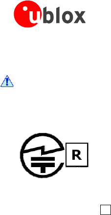
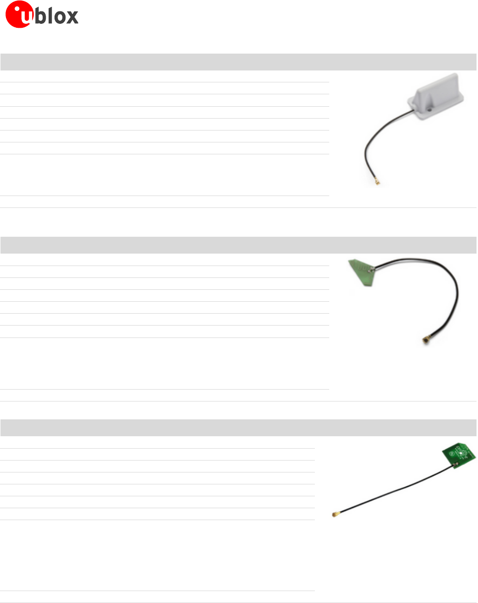
7.1 Antenna accessories
Name
U.FL to SMA adapter cable
Connector
U.FL and SMA jack (outer thread and pin receptacle)
Impedance
50 Ω
Minimum cable loss
0.5 dB, The cable loss must be above the minimum cable
loss to meet the regulatory requirements. Minimum cable
length 100 mm.
Comment
The SMA connector can be mounted in a panel.
See NINA-B2 series System Integration Manual [1] for
information how to integrate the U.FL connector.
Approval
RED, MIC and NCC
NINA-B2 series - Data Sheet
UBX-18006649 - R01 Antennas
Page 29 of 41
Name
U.FL to Reverse Polarity SMA adapter cable
Connector
U.FL and Reverse Polarity SMA jack (outer thread and pin)
Impedance
50 Ω
Minimum cable loss
0.5 dB, The cable loss must be above the minimum cable
loss to meet the regulatory requirements. Minimum cable
length 100 mm.
Comment
The Reverse Polarity SMA connector can be mounted in a
panel.
See NINA-B2 series System Integration Manual [1] for
information how to integrate the U.FL connector. It is
required to followed this reference design to comply with
the NINA-B22 FCC/IC modular approvals.
Approval
FCC, IC, RED, MIC and NCC
7.2 Approved antennas
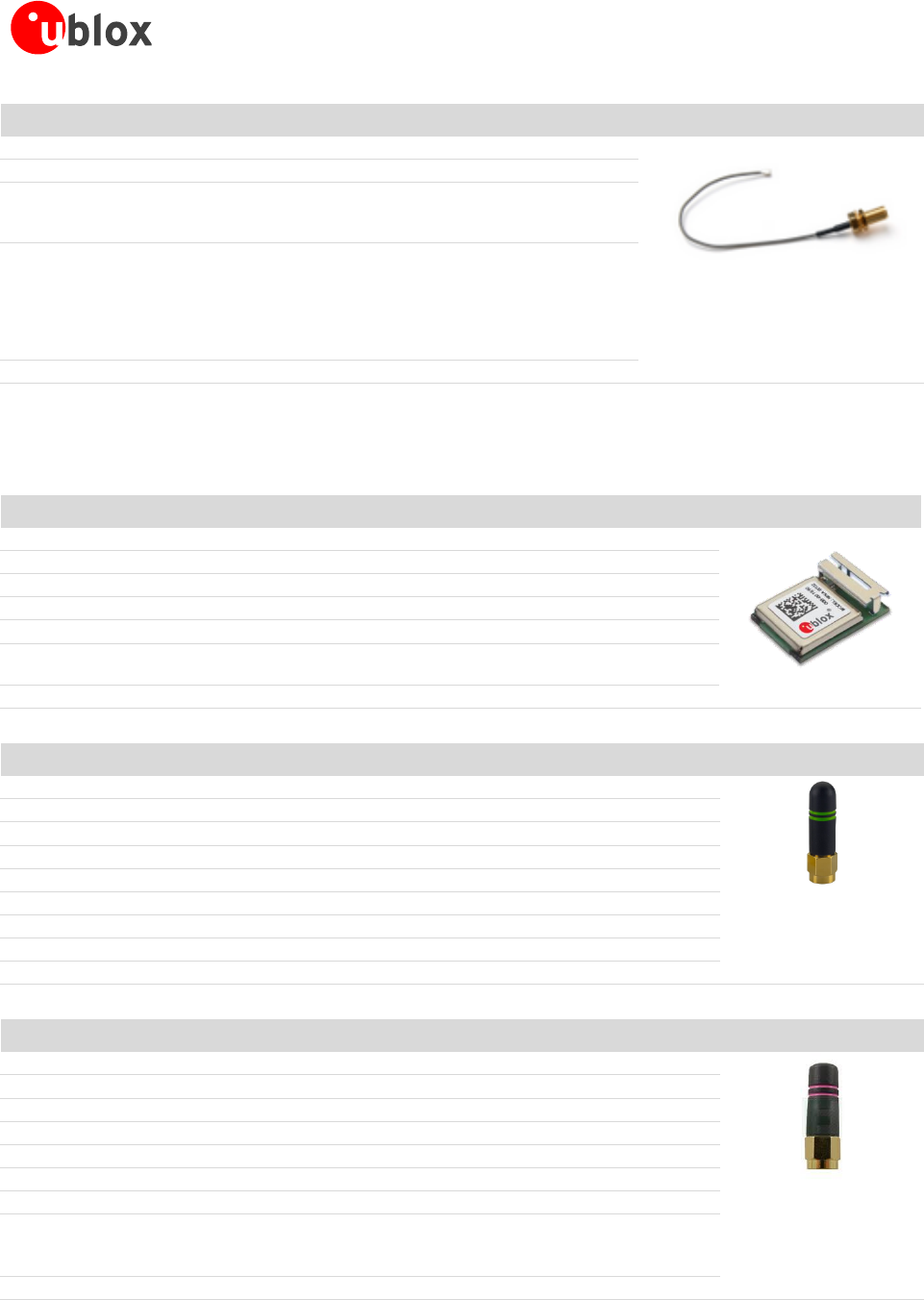
7.2.1 Single band antennas
NINA-B222
Manufacturer
ProAnt
Gain
+3 dBi
Impedance
50 Ω
Size (HxWxL)
3.0 x 3.8 x 9.9 mm
Type
PIFA
Comment
SMD PIFA antenna on NINA-B222. Should not be mounted inside a metal enclosure, see
section for more info 2.5.1.
Approval
FCC, IC, RED, MIC and NCC
GW.26.0111
Manufacturer
Taoglas
Polarization
Vertical
Gain
+2.0 dBi
Impedance
50 Ω
Size
Ø 7.9 x 30.0 mm
Type
Monopole
Connector
SMA (M) .
Comment
To be mounted on the U.FL to SMA adapter cable.
Approval
FCC, IC, RED, MIC, and NCC
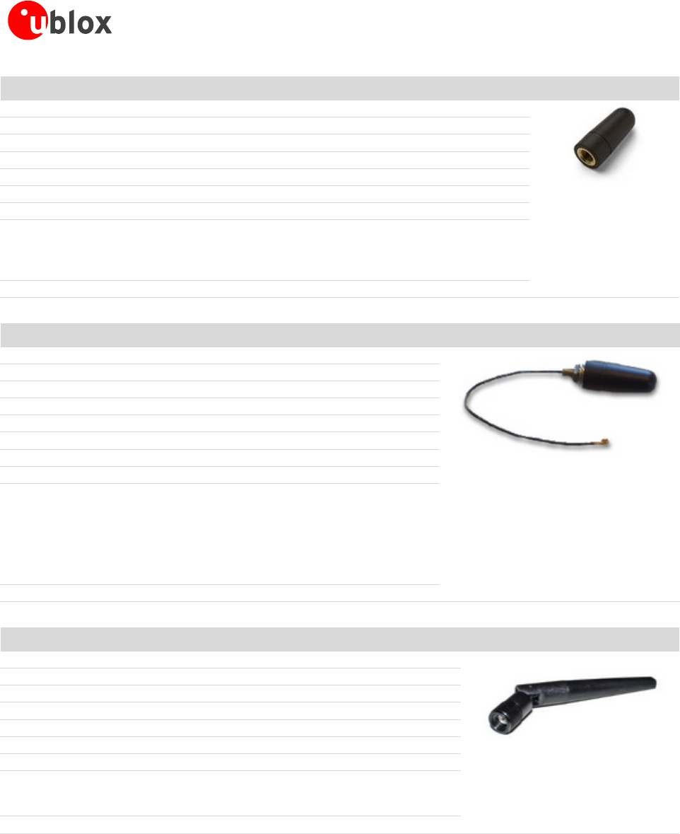
ANT-2.4-CW-RH-RPS
Manufacturer
Linx
Polarization
Vertical
Gain
-1.0 dBi
Impedance
50 Ω
Size
Ø 7.4 x 27.0 mm
Type
Monopole
Connector
Reverse Polarity SMA plug (inner thread and pin receptacle).
Comment
To be mounted on the U.FL to Reverse Polarity SMA adapter cable.
An SMA version antenna is also available but not recommended for use (ANT-2.4-CW-
RH-SMA).
Approval
FCC, IC, RED, MIC and NCC
NINA-B2 series - Data Sheet
UBX-18006649 - R01 Antennas
Page 30 of 41
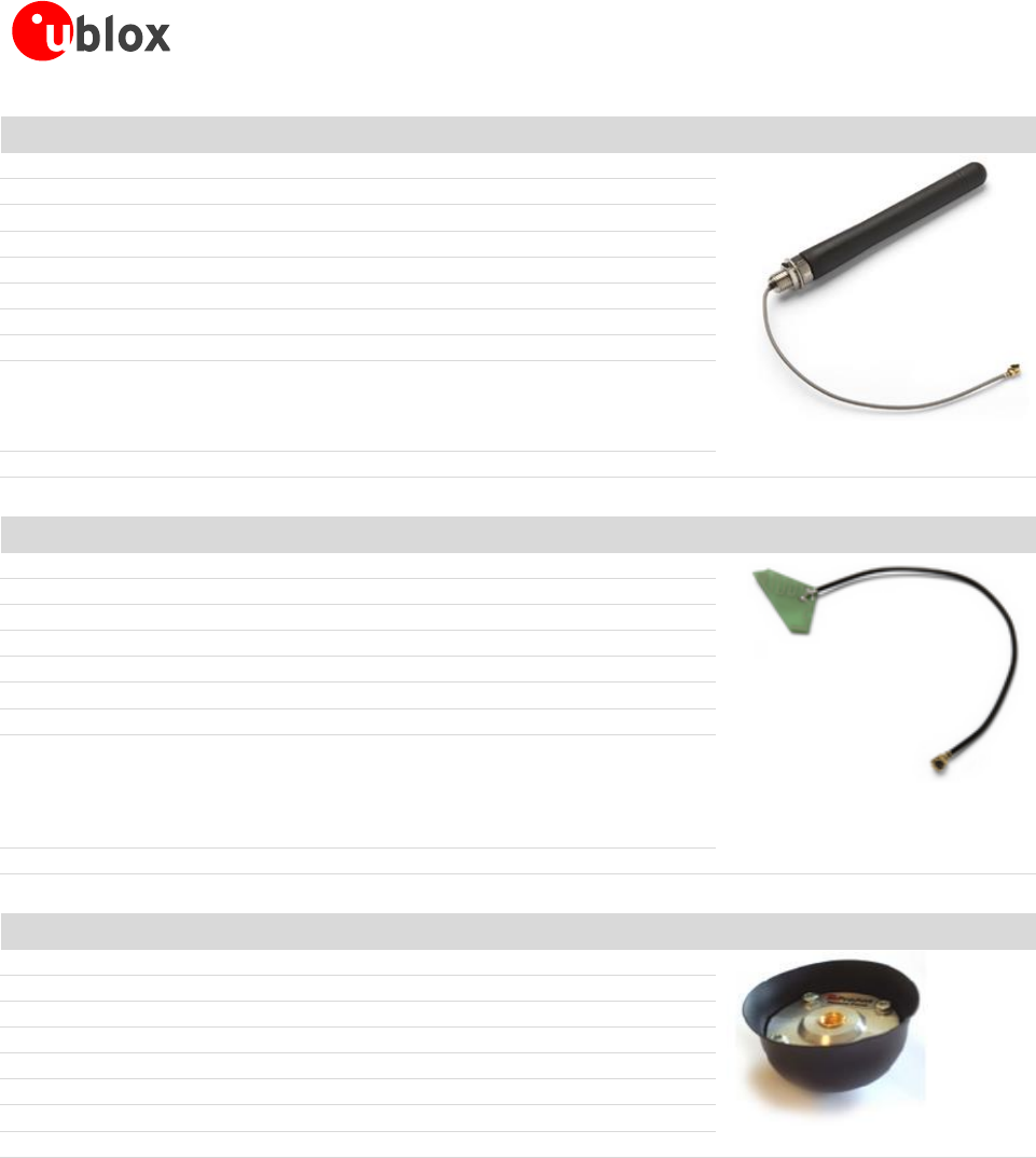
Ex-IT 2400 RP-SMA 28-001
Manufacturer
ProAnt
Polarization
Vertical
Gain
+3.0 dBi
Impedance
50 Ω
Size
Ø 12.0 x 28.0 mm
Type
Monopole
Connector
Reverse Polarity SMA plug (inner thread and pin receptacle).
Comment
This antenna requires to be mounted on a metal ground plane for best performance.
To be mounted on the U.FL to Reverse Polarity SMA adapter cable.
An SMA version antenna is also available but not recommended for use (Ex-IT 2400
SMA 28-001).
Approval
FCC, IC, RED, MIC and NCC
Ex-IT 2400 MHF 28
Manufacturer
ProAnt
Polarization
Vertical
Gain
+2.0 dBi
Impedance
50 Ω
Size
Ø 12.0 x 28.0 mm
Type
Monopole
Cable length
100 mm
Connector
U.FL. connector
Comment
This antenna requires to be mounted on a metal ground plane for
best performance.
To be mounted on a U.FL connector.
See NINA-B2 series System Integration Manual [1] for information
how to integrate the U.FL connector. It is required to followed this
reference design to comply with the NINA -W13 FCC/IC modular
approvals.
Approval
FCC, IC, RED, MIC and NCC
Ex-IT 2400 RP-SMA 70-002
Manufacturer
ProAnt
Polarization
Vertical
Gain
+3.0 dBi
Impedance
50 Ω
Size
Ø 10 x 83 mm
Type
Monopole
Connector
Reverse Polarity SMA plug (inner thread and pin receptacle)
Comment
To be mounted on the U.FL to Reverse Polarity SMA adapter cable.
An SMA version antenna is also available but not recommended for use
(Ex-IT 2400 SMA 70-002).
Approval
FCC, IC, RED, MIC and NCC
NINA-B2 series - Data Sheet
UBX-18006649 - R01 Antennas
Page 31 of 41
Ex-IT 2400 MHF 70-001
Manufacturer
ProAnt
Polarization
Vertical
Gain
+3.0 dBi
Impedance
50 Ω
Size
Ø 9.4 x 70.5 mm
Type
Monopole
Cable length
100 mm
Connector
U.FL. connector
Comment
To be mounted on a U.FL connector.
See NINA-B2 series System Integration Manual [1] for information how to
integrate the U.FL connector. It is required to followed this reference design
to comply with the NINA-B2 FCC/IC modular approvals.
Approval
FCC, IC, RED, MIC and NCC
InSide-2400
Manufacturer
ProAnt
Gain
+3.0 dBi
Impedance
50 Ω
Size
27 x 12 mm (triangular)
Type
Patch
Cable length
100 mm
Connector
U.FL. connector
Comment
Should be attached to a plastic enclosure or part for best performance.
To be mounted on a U.FL connector.
See NINA-B2 series System Integration Manual [1] for information how to
integrate the U.FL connector. It is required to followed this reference design
to comply with the NINA-B2 FCC/IC modular approvals.
Approval
FCC, IC, RED, MIC and NCC
FlatWhip-2400
Manufacturer
ProAnt
Gain
+3.0 dBi
Impedance
50 Ω
Size
Ø 50.0 x 30.0 mm
Type
Monopole
Connector
SMA plug (inner thread and pin)
Comment
To be mounted on the U.FL to SMA adapter cable.
Approval
RED, MIC and NCC
NINA-B2 series - Data Sheet
UBX-18006649 - R01 Antennas
Page 32 of 41
Outside-2400
Manufacturer
ProAnt
Gain
+3.0 dBi
Impedance
50 Ω
Size
36.0 x 18.0 x 16.0 mm
Type
Patch
Cable length
70 mm
Connector
U.FL. connector
Comment
To be mounted on a U.FL connector.
See NINA-B2 series System Integration Manual [1] for information how to
integrate the U.FL connector. It is required to followed this reference design
to comply with the NINA-B2 FCC/IC modular approvals.
Approval
FCC, IC, RED, MIC and NCC
7.2.2 Dual-band antennas
InSide-WLAN
Manufacturer
ProAnt
Gain
+3.0 dBi
Impedance
50 Ω
Size
27 x 12 mm (triangular)
Type
Patch
Cable length
100 mm
Connector
U.FL. connector
Comment
Should be attached to a plastic enclosure or part for best performance.
Dual-band (2.4 GHz / 5 GHz) antenna to be mounted on a U.FL connector.
See NINA-B2 series System Integration Manual [1] for information how to
integrate the U.FL connector. It is required to followed this reference design
to comply with the NINA-B2 FCC/IC modular approvals.
Approval
FCC, IC, RED, MIC and NCC
InSide-WLAN Square
Manufacturer
ProAnt
Gain
+3.0 dBi
Impedance
50 Ω
Size
24x22x1 mm with mounting hole
Type
Patch
Cable length
100 mm
Connector
U.FL. connector
Comment
Should be attached to a plastic enclosure or part for best performance.
Dual-band (2.4 GHz / 5 GHz) antenna to be mounted on a U.FL
connector.
See NINA-B2 series System Integration Manual [1] for information on
how to integrate the U.FL connector. It is required to followed this
reference design to comply with the NINA-B2 FCC/IC modular
approvals.
Approval
FCC, IC, RED, MIC and NCC
NINA-B2 series - Data Sheet
UBX-18006649 - R01 Antennas
Page 33 of 41
Ex-IT WLAN RPSMA
Manufacturer
ProAnt
Type
½ wave dipole dual-band antenna
Polarization
Vertical
Gain
+3 dBi
Impedance
50 Ω
Size
107 mm (Straight)
Type
Monopole
Connector
Reverse Polarity SMA plug (inner thread and pin receptacle)
Comment
To be mounted on the U.FL to Reverse Polarity SMA adapter cable.
Approval
FCC, IC, RED, MIC and NCC
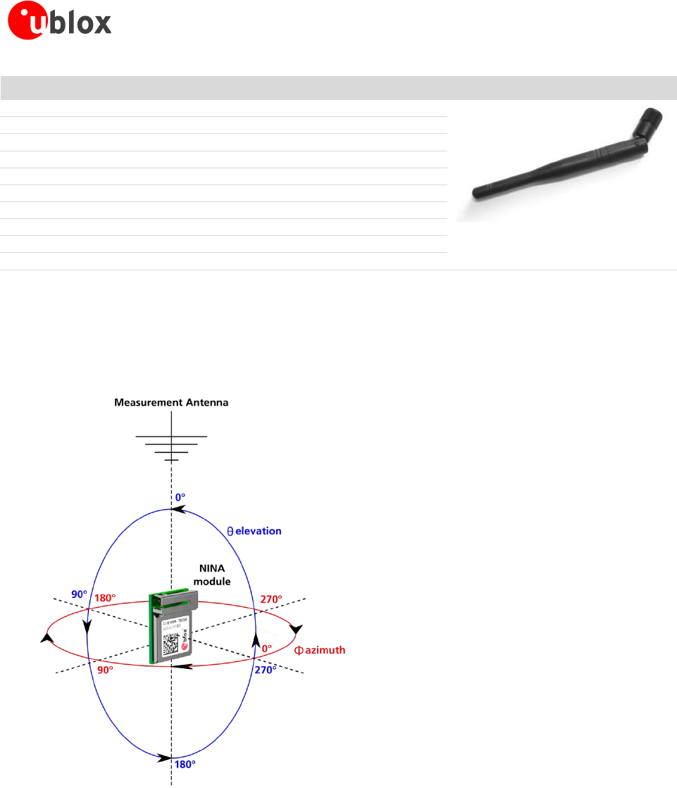
7.3 NINA-B222 radiation patterns
The below radiation patterns show the relative output power of an EVB-NINA-B222 transmitting at 0 dBm
output power. Both horizontal and vertical antenna polarizations were used. The
NINA-B2 module was rotated 360° around the azimuth axis while being kept at 0°, 90° and 180° elevation as
shown in Figure 8.
Figure 8: Azimuth and elevation rotation axes relative to the measurement antenna
NINA-B2 series - Data Sheet
UBX-18006649 - R01 Product handling
Page 34 of 41
8 Product handling
8.1 Packaging
The NINA-B2 series modules are in development status as mentioned in the table on page 2.
Hence, the information in this section will be applicable only when the module is fully tested and
approved in the Initial Production stage.
8.1.1 Reels
The NINA-B2 series modules are delivered as hermetically sealed, reeled tapes to enable efficient production,
production lot set-up and tear-down. For more information about packaging, see the u-blox Package
Information Guide [2].
NINA-B2 modules are deliverable in quantities of 500 pieces on a reel. The reel types for the NINA-B2 modules
are provided in Table 21 and detailed information about the reel types are described in u-blox Package
Information Guide [2].
Model
Reel Type
NINA-B221
B
NINA-B222
A
Table 21: Reel types for the different models of NINA-B2 series
8.1.2 Tapes
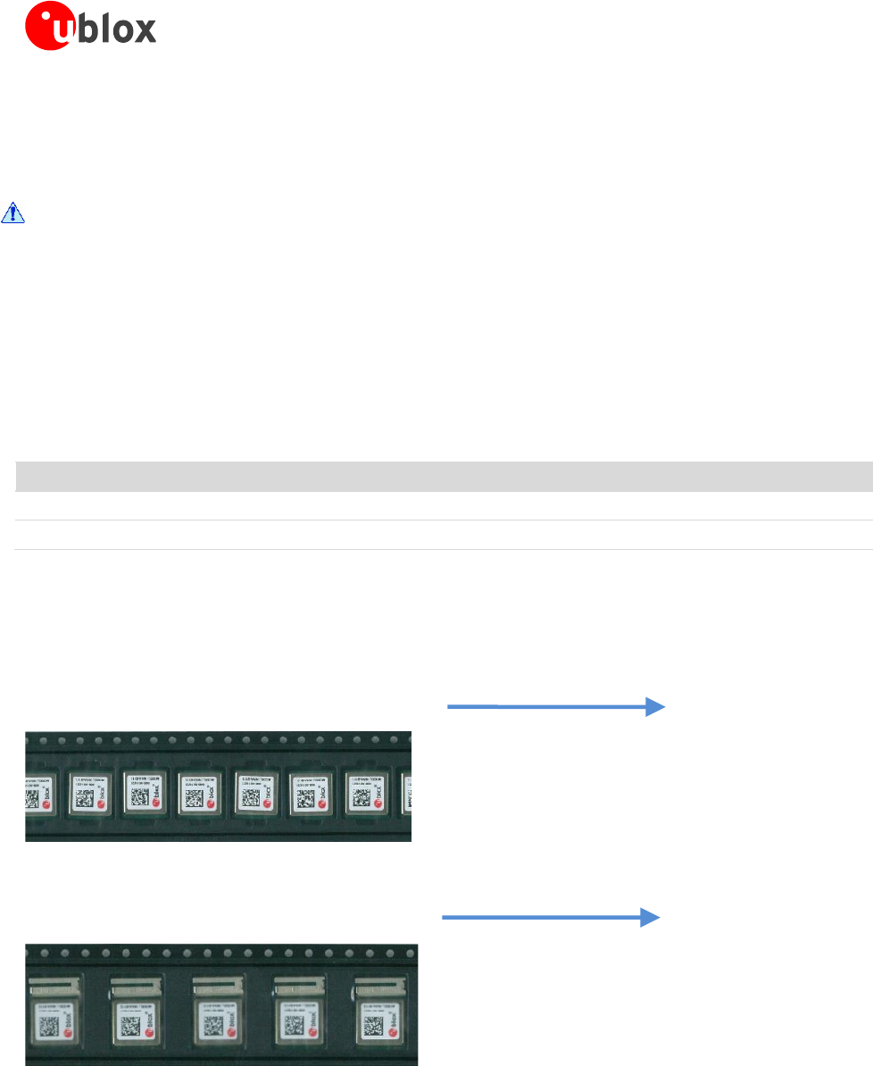
Figure 9 and Figure 10 shows the position and orientation of the NINA-B2 modules as they are delivered on
tape. The dimensions of the tapes are specified in Figure 11 and Figure 12.
Figure 9: Orientation of NINA-B221 module on tape
Figure 10: Orientation of NINA-B222 module on tape
Feed direction
Feed direction
NINA-B2 series - Data Sheet
UBX-18006649 - R01 Product handling
Page 35 of 41
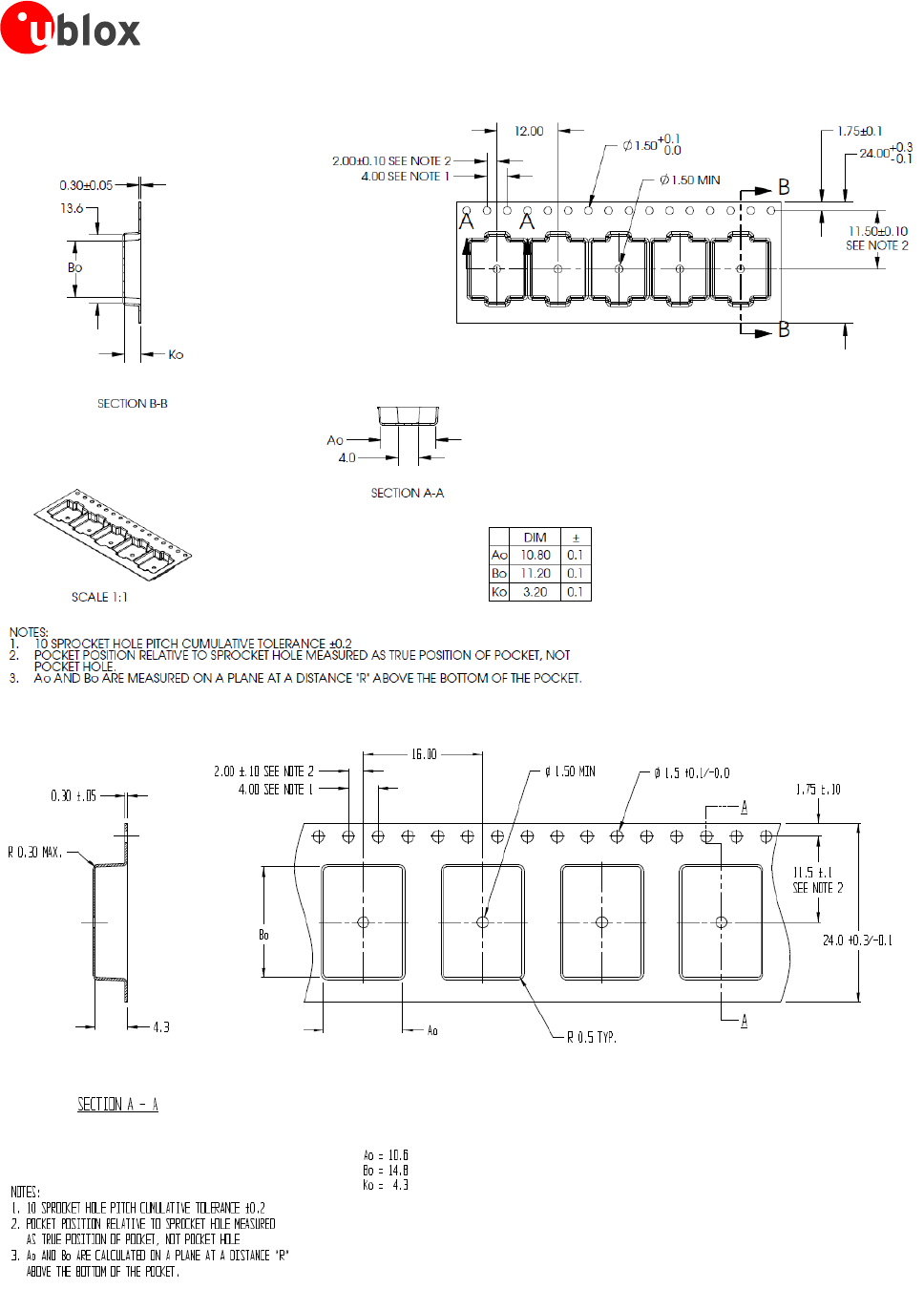
Figure 11: NINA-B221 tape dimension
Figure 12: NINA-B222 tape dimension

NINA-B2 series - Data Sheet
UBX-18006649 - R01 Product handling
Page 36 of 41
8.2 Moisture sensitivity levels
The NINA-B2 series modules are Moisture Sensitive Devices (MSD) in accordance with the
IPC/JEDEC specification.
The Moisture Sensitivity Level (MSL) relates to the required packaging and handling precautions. The NINA-B2
series modules are rated at MSL level 4. For more information regarding moisture sensitivity levels, labeling and
storage, see the u-blox Package Information Guide [2].
For MSL standards, see IPC/JEDEC J-STD-020, which can be downloaded from www.jedec.org.
8.3 Reflow soldering
Reflow profiles are to be selected according to u-blox recommendations. See NINA-B2 series System Integration
Manual [1] for more information.
Failure to observe these recommendations can result in severe damage to the device.
8.4 ESD precautions
The NINA-B2 series modules contain highly sensitive electronic circuitry and are Electrostatic
Sensitive Devices (ESD). Handling the NINA-B2 series modules without proper ESD protection may
destroy or damage them permanently.
The NINA-B2 series modules are electrostatic sensitive devices (ESD) and require special ESD precautions typically
applied to ESD sensitive components. Section 4.1.1 provides the maximum ESD ratings of the
NINA-B2 series modules.
Proper ESD handling and packaging procedures must be applied throughout the processing, handling and
operation of any application that incorporates the NINA-B2 series module. The ESD precautions should be
implemented on the application board where the module is mounted as described in the
NINA-B2 series System Integration Manual [1].
Failure to observe these recommendations can result in severe damage to the device.
NINA-B2 series - Data Sheet
UBX-18006649 - R01 Labeling and ordering information
Page 37 of 41
9 Labeling and ordering information
9.1 Product labeling
The labels (7.5x7.5mm) of the NINA-B2 series modules include important product information as described in
this section.
Figure 8 illustrates the label of all the NINA-B2 series modules, which includes product type number and revision,
production date, Data Matrix with unique serial number (MAC address) and the u-blox logo.
Figure 13: Location of product type number on the NINA-B2 series module label
Reference
Description
1
Date of unit production encoded YY/WW (year, week)
2
Major and minor product version info
3
Product model name (NINA-B221 or NINA-B222)
4
Data Matrix with unique serial number of 19 alphanumeric symbols. The first 3 symbols represent the unique
module type number:
TBD: NINA-B221
TBD: NINA-B222
The next 12 symbols represent the unique hexadecimal Bluetooth address of the module AABBCCDDEEFF, and
the last 4 symbols represent the hardware and software version encoded HHFF.
See section 1.8 for more information about addresses.
5
u-blox logo. The red dot is also indicating pin no 1.
Table 22: NINA-B2 series label description
3
1
2
4
5
NINA-B2 series - Data Sheet
UBX-18006649 - R01 Labeling and ordering information
Page 38 of 41
9.2 Explanation of codes
Three different product code formats are used. The Product Name is used in documentation such as this data
sheet and identifies all u-blox products, independent of packaging and quality grade. The Ordering Code
includes options and quality, while the Type Number includes the hardware and software versions. Table 23
below details these three different formats:
Format
Structure
Product Name
PPPP-TGVV
Ordering Code
PPPP -TGVV-TTQ
Type Number
PPPP -TGVV-TTQ-XX
Table 23: Product code formats
Table 24 explains the parts of the product code.
Code
Meaning
Example
PPPP
Form factor
NINA
TG
Platform (Technology and Generation)
T – Dominant technology, For example, W: Wi-Fi, B: Bluetooth
G - Generation
B2: Bluetooth Generation 2
VV
Variant based on the same platform; range [00…99]
21: u-blox connectivity software product with antenna pin
TT
Major Product Version
00: first revision
Q
Quality grade
A: Automotive
B: Professional
C: Standard
B: professional grade
XX
Minor product version (not relevant for certification)
Default value is 00
Table 24: Part identification code
9.3 Ordering information
Ordering Code
Product
NINA-B221-00B-00
Bluetooth dual-mode module with antenna pin. With u-blox connectivity software including secure boot.
NINA-B222-00B-00
Bluetooth dual-mode module module with internal onboard antenna. With u-blox connectivity software including
secure boot.
Table 25: Product ordering codes

NINA-B2 series - Data Sheet
UBX-18006649 - R01 Appendix
Page 39 of 41
Appendix
A Glossary
Abbreviation
Definition
ADC
Analog to Digital Converter
BLE
Bluetooth Low Energy
BPF
Band Pass Filter
BT
Bluetooth
CTS
Clear To Send
DAC
Digital to Analog Converter
DC
Direct Current
DSR
Data Set Ready
DTR
Data Terminal Ready
ESD
Electro Static Discharge
FCC
Federal Communications Commission
GND
Ground
GPIO
General Purpose Input/Output
I
Input (means that this is an input port of the module)
I2C
Inter-Integrated Circuit
IC
Industry Canada
IEEE
Institute of Electrical and Electronics Engineers
IoT
Internet of Things
L
Low
LPO
Low Power Oscillator
MCU
Micro Controller Unit
MDIO
Management Data Input / Output
MII
Media-Independent Interface
MRD
Market Requirement Document
MSD
Moisture Sensitive Device
N/A
Not Applicable
O
Output (means that this is an output port of the module)
PCN
Product Change Notification
PD
Pull-Down
PU
Pull-Up
QSPI
Quad Serial Peripheral Interface
RTS
Request To Send
RXD
Receive Data
SDIO
Secure Digital Input Output
SDK
Software Development Kit
SPI
Serial Peripheral Interface
TBD
To Be Defined
TXD
Transmit Data
UART
Universal Asynchronous Receiver/Transmitter
Table 26: Explanation of abbreviations used

NINA-B2 series - Data Sheet
UBX-18006649 - R01 Related documents
Page 40 of 41
Related documents
[1] NINA-B2 Series System Integration Manual, UBX-18011096
[2] u-blox Package Information Guide, document number UBX-14001652
[3] u-blox Short Range AT Commands Manual, document number UBX-14044127
For regular updates to u-blox documentation and to receive product change notifications, register on our
homepage (http://www.u-blox.com).

NINA-B2 series - Data Sheet
UBX-18006649 - R01 Contact
Page 41 of 41
Contact
For complete contact information visit us at www.u-blox.com.
u-blox Offices
North, Central and South America
u-blox America, Inc.
Phone: +1 703 483 3180
E-mail: info_us@u-blox.com
Regional Office West Coast:
Phone: +1 408 573 3640
E-mail: info_us@u-blox.com
Technical Support:
Phone: +1 703 483 3185
E-mail: support_us@u-blox.com
Headquarters
Europe, Middle East, Africa
u-blox AG
Phone: +41 44 722 74 44
E-mail: info@u-blox.com
Support: support@u-blox.com
Asia, Australia, Pacific
u-blox Singapore Pte. Ltd.
Phone: +65 6734 3811
E-mail: info_ap@u-blox.com
Support: support_ap@u-blox.com
Regional Office Australia:
Phone: +61 2 8448 2016
E-mail: info_anz@u-blox.com
Support: support_ap@u-blox.com
Regional Office China (Beijing):
Phone: +86 10 68 133 545
E-mail: info_cn@u-blox.com
Support: support_cn@u-blox.com
Regional Office China (Chongqing):
Phone: +86 23 6815 1588
E-mail: info_cn@u-blox.com
Support: support_cn@u-blox.com
Regional Office China (Shanghai):
Phone: +86 21 6090 4832
E-mail: info_cn@u-blox.com
Support: support_cn@u-blox.com
Regional Office China (Shenzhen):
Phone: +86 755 8627 1083
E-mail: info_cn@u-blox.com
Support: support_cn@u-blox.com
Regional Office India:
Phone: +91 80 4050 9200
E-mail: info_in@u-blox.com
Support: support_in@u-blox.com
Regional Office Japan (Osaka):
Phone: +81 6 6941 3660
E-mail: info_jp@u-blox.com
Support: support_jp@u-blox.com
Regional Office Japan (Tokyo):
Phone: +81 3 5775 3850
E-mail: info_jp@u-blox.com
Support: support_jp@u-blox.com
Regional Office Korea:
Phone: +82 2 542 0861
E-mail: info_kr@u-blox.com
Support: support_kr@u-blox.com
Regional Office Taiwan:
Phone: +886 2 2657 1090
E-mail: info_tw@u-blox.com
Support: support_tw@u-blox.com