u blox TOBYL201 UMTS/LTE Data Module User Manual TOBY L2 series
u-blox AG UMTS/LTE Data Module TOBY L2 series
UserManual.wiki
>
u blox
>
TOBYL201 User Manual
>
Datasheet
Contents
1.
Datasheet
2.
Integrators Manual
3.
TempConfidential_TOBY-L2-MPCI-L2_SysIntegrManual_UBX-13004618
Datasheet
Navigation menu
Upload a User Manual
Namespaces
Wiki Guide
HTML
PDF
Info
Views
User Manual
Discussion / Help
Navigation
![TOBY-L2 series - Data Sheet UBX-13004573 - R07 Objective Specification Functional description Page 8 of 47 4G LTE 3G UMTS/HSDPA/HSUPA 2G GSM/GPRS/EDGE LTE Power Class Power Class 3 (23 dBm) for LTE mode WCDMA/HSDPA/HSUPA Power Class Power Class 3 (24 dBm) for UMTS/HSDPA/HSUPA mode GSM/GPRS (GMSK) Power Class Power Class 4 (33 dBm) for GSM/E-GSM bands Power Class 1 (30 dBm) for DCS/PCS bands EDGE (8-PSK) Power Class Power Class E2 (27 dBm) for GSM/E-GSM bands Power Class E2 (26 dBm) for DCS/PCS bands Data rate LTE category 4: up to 150 Mb/s DL, 50 Mb/s UL Data Rate TOBY-L200 and TOBY-L201: HSDPA cat.14, up to 21 Mb/s DL1 HSUPA cat.6, up to 5.6 Mb/s UL TOBY-L210 and TOBY-L280: HSDPA cat.24, up to 42 Mb/s DL HSUPA cat.6, up to 5.6 Mb/s UL Data Rate2 GPRS multi-slot class 123, CS1-CS4, up to 85.6 kb/s DL/UL EDGE multi-slot class 123, MCS1-MCS9, up to 236.8 kb/s DL/UL Table 2: TOBY-L2 series LTE, 3G and 2G characteristics 1.5 AT command support The TOBY-L2 series modules support AT commands according to 3GPP standards TS 27.007 [10], TS 27.005 [11] and the u-blox AT command extension. For the complete list of all supported AT commands and their syntax, see the u-blox AT Commands Manual [1]. RIL (Radio Interface Layer) software for Android and Embedded Windows is available for TOBY-L2 series modules free of charge; see the Android RIL Production delivery [3] and Windows Embedded RIL Production delivery [4] application notes for the supported software deliveries and more information. 1 HSDPA category 24 capable 2 GPRS/EDGE multi-slot class determines the number of timeslots available for upload and download and thus the speed at which data can be transmitted and received, with higher classes typically allowing faster data transfer rates. 3 GPRS/EDGE multi-slot class 12 implies a maximum of 4 slots in DL (reception) and 4 slots in UL (transmission) with 5 slots in total.](https://usermanual.wiki/u-blox/TOBYL201.Datasheet/User-Guide-2644987-Page-8.png)
![TOBY-L2 series - Data Sheet UBX-13004573 - R07 Objective Specification Functional description Page 9 of 47 1.6 Supported features Table 3 lists the main features supported by TOBY-L2 modules. For more details see TOBY-L2 / MPCI-L2 series System Integration Manual [2] and u-blox AT Commands Manual [1]. Feature Description Network Indication4 GPIO configured to indicate the network status: registered home network, registered roaming, voice or data call enabled, no service. The feature can be enabled through the +UGPIOC AT command. Antenna Detection5 The ANT_DET pin provides antenna presence detection capability, evaluating the resistance from ANT1 and ANT2 pins to GND by means of an external antenna detection circuit implemented on the application board. The antenna detection feature can be enabled through the +UANTR AT command. Jamming detection5 Detects “artificial” interference that obscures the operator’s carriers entitled to give access to the radio service and reports the start and stop of such conditions to the application processor (AP). The AP can react appropriately by e.g. switching off the radio transceiver to reduce power consumption and monitoring the environment at regular intervals. The feature can be enabled and configured through the +UCD AT command. Embedded TCP and UDP stack6 Embedded TCP/IP and UDP/IP stack including direct link mode for TCP and UDP sockets. Sockets can be set in Direct Link mode to establish a transparent end to end communication with an already connected TCP or UDP socket via serial interface. FTP6, FTPS5 File Transfer Protocol as well as Secure File Transfer Protocol (SSL encryption of FTP control channel) functionalities are supported via AT commands. HTTP6, HTTPS5 Hyper-Text Transfer Protocol as well as Secure Hyper-Text Transfer Protocol (SSL encryption) functionalities are supported via AT commands. HEAD, GET, POST, DELETE and PUT operations are available. GNSS via modem5 Full access to u-blox positioning chips and modules is available through a dedicated DDC (I2C) interface. This means that from any host processor a single serial port can control the cellular module and the positioning chip or module. For more details see the GNSS Implementation Application Note [5]. Embedded AssistNow Software5 Embedded AssistNow Online and AssistNow Offline clients are available to provide better GNSS performance and faster Time-to-First-Fix. An AT command can enable / disable the clients. CellLocate®5 Enables the estimation of device position based on the parameters of the mobile network cells visible to the specific device based on the CellLocate® database: Normal scan: only the parameters of the visible home network cells are sent Deep scan: the parameters of all surrounding cells of all mobile operators are sent CellLocate® is available via a set of AT commands for CellLocate® service configuration and position request. Hybrid Positioning5 The current module position is provided by a u-blox positioning chip or module or the estimated position from CellLocate® depending on which method provides the best and fastest solution according to the user configuration. Hybrid positioning is available via a set of AT commands that allow the configuration and the position request. Wi-Fi via modem7 Full access to u-blox short range communication Wi-Fi modules is available through a dedicated SDIO interface. This means that from any host processor a single serial port can control the cellular module and the short range communication module. All the management software for the Wi-Fi module operations runs inside the cellular module in addition to those required for cellular-only operation: Wi-Fi driver, Web User Interface (WebUI), Connection Config Manager. For more details see the Wi-Fi / Cellular Integration Application Note [8]. Firmware update Over AT commands (FOAT) Firmware module update over AT command interfaces (UART, USB). The feature can be enabled and configured through the +UFWUPD AT command. Firmware update Over The Air (FOTA)6 Firmware module update over the LTE/3G/2G air interface. The feature can be enabled and configured through the +UFWINSTALL AT command. LTE DL MIMO 2x2 and 3G DL Rx Diversity Improved cellular link quality and reliability on all operating bands. 4 Not supported by “50” product versions 5 Not supported by “00”, “01” and “50” product versions. 6 Not supported by “00” and “50” product versions. 7 Not supported by “00” and “01” product versions.](https://usermanual.wiki/u-blox/TOBYL201.Datasheet/User-Guide-2644987-Page-9.png)
![TOBY-L2 series - Data Sheet UBX-13004573 - R07 Objective Specification Functional description Page 10 of 47 Feature Description Smart Temperature Supervisor8 Constant monitoring of the module board temperature: Warning notification when the temperature approaches an upper or lower predefined threshold Shutdown notified and forced when the temperature value is outside the specified range (shutdown suspended in case of an emergency call in progress) The Smart Temperature Supervisor feature can be enabled and configured through the +USTS AT command. The sensor measures board temperature, which can differ from ambient temperature. SIM Access Profile (SAP)8 Allows access and use of a remote SIM card/chip instead of the local SIM card/chip directly connected to the module SIM interface. The module acts as an SAP client establishing a connection and performing data exchange to an SAP server directly connected to the remote SIM. The modules provide a dedicated USB SAP channel and dedicated multiplexer SAP channel over UART for communication with the remote SIM card. In-Band Modem8 In-Band modem solution for eCall and ERA-GLONASS emergency call applications over cellular networks implemented according to the 3GPP TS 26.267 specification [13] When activated, the in-vehicle eCall / ERA-GLONASS system (IVS) creates an emergency call carrying both voice and data (including vehicle position data) directly to the nearest Public Safety Answering Point (PSAP) to determine whether rescue services should be dispatched to the known position. Power saving The power saving configuration is by default disabled, but it can be enabled and configured using the +UPSV AT command. When the power saving is enabled, the module automatically enters the low power idle-mode whenever possible, reducing current consumption. During idle-mode, the module processor core runs with the RTC 32 kHz reference clock, which is generated by the internal 32 kHz oscillator. SMS via IMS9 Allows SMS via embedded IP Multimedia Subsystem Table 3: TOBY-L2 series main supported features u-blox is extremely mindful of user privacy. When a position is sent to the CellLocate® server u-blox is unable to track the SIM used or the specific device. 8 Not supported by “00”, “01” and “50” product versions. 9 Not supported by “00” and “50” product versions.](https://usermanual.wiki/u-blox/TOBYL201.Datasheet/User-Guide-2644987-Page-10.png)
![TOBY-L2 series - Data Sheet UBX-13004573 - R07 Objective Specification Interfaces Page 11 of 47 2 Interfaces 2.1 Power management 2.1.1 Module supply input (VCC) TOBY-L2 series modules must be supplied through the VCC pins by a DC power supply. Voltage must be stable, because during operation the current drawn from VCC can vary significantly, based on the power consumption profile of the LTE/3G/2G technologies (described in the TOBY-L2 / MPCI-L2 series System Integration Manual [2]). 2.1.2 RTC supply input / output (V_BCKP) When VCC voltage is within the valid operating range, the internal Power Management Unit (PMU) supplies the Real Time Clock (RTC) and the same supply voltage is available on the V_BCKP pin. If the VCC voltage is under the minimum operating limit (e.g. during not powered mode), the V_BCKP pin can externally supply the RTC. 2.1.3 Generic digital interfaces supply output (V_INT) TOBY-L2 series modules provide a 1.8 V supply rail output on the V_INT pin, which is internally generated when the module is switched on. The same voltage domain is used internally to supply the generic digital interfaces of the modules. The V_INT supply output can be used in place of an external discrete regulator. 2.2 Antenna interfaces 2.2.1 Antenna RF interfaces The modules have two RF pins with a characteristic impedance of 50 . The primary antenna pin (ANT1) supports both Tx and Rx, providing the main antenna interface, while the secondary antenna pin (ANT2) supports Rx only for the LTE MIMO 2x2 and 3G Rx diversity configurations. 2.2.2 Antenna detection The antenna detection is not supported by “00”, “01” and “50” product versions. The ANT_DET pin is an Analog to Digital Converter (ADC) input with a current source provided by TOBY-L2 modules to sense the antenna presence (as an optional feature). It evaluates the resistance from ANT1 and ANT2 pins to GND by means of an external antenna detection circuit implemented on the application board. (For more details, see the TOBY-L2 / MPCI-L2 series System Integration Manual [2] and the u-blox AT Commands Manual [1].) 2.3 System functions 2.3.1 Module power-on TOBY-L2 series can be switched on in one of the following ways: Rising edge on the VCC pin to a valid voltage for module supply, i.e. applying module supply Low level on the PWR_ON pin, which is normally set high by an internal pull-up, for a valid time period when the applied VCC voltage is within the valid operating range (see section 4.2.8). The PWR_ON line should be driven by open drain, open collector or contact switch.](https://usermanual.wiki/u-blox/TOBYL201.Datasheet/User-Guide-2644987-Page-11.png)
![TOBY-L2 series - Data Sheet UBX-13004573 - R07 Objective Specification Interfaces Page 12 of 47 Low level on the RESET_N pin, which is normally set high by an internal pull-up, for a valid time period when the applied VCC voltage is within the valid operating range (see section 4.2.9). The RESET_N line should be driven by open drain, open collector or contact switch. RTC alarm, i.e. pre-programmed scheduled time by AT+CALA command 2.3.2 Module power-off TOBY-L2 series can be properly switched off by: AT+CPWROFF command (see the u-blox AT Commands Manual [1]). The current parameter settings are saved in the module’s non-volatile memory and a proper network detach is performed. An abrupt under-voltage shutdown occurs on TOBY-L2 series modules when the VCC supply is removed. If this occurs, it is not possible to store the current parameter settings in the module’s non-volatile memory or to perform the proper network detach. An abrupt shutdown occurs on TOBY-L2 series modules when a low level is applied on the RESET_N pin, which is normally set high by an internal pull-up, for a valid time period (see the section 4.2.9). This causes an abrupt shutdown of the module: the current parameter settings are not saved in the module’s non-volatile memory and a proper network detach is not performed. An over-temperature or an under-temperature shutdown occurs on TOBY-L2 modules when the temperature measured within the cellular module reaches the dangerous area, if the optional Smart Temperature Supervisor feature is enabled and configured by the dedicated AT command. For more details see the TOBY-L2 / MPCI-L2 series System Integration Manual [2] and the u-blox AT Commands Manual [1], +USTS AT command. Smart Temperature Supervisor is not supported by “00”, “01” and “50” product versions. 2.3.3 Module reset TOBY-L2 series modules can be reset (rebooted) by: AT+CFUN command (see the u-blox AT Commands Manual [1]). This causes an “internal” or “software” reset of the module. The current parameter settings are saved in the module’s non-volatile memory and a proper network detach is performed. An abrupt “external” or “hardware” reset occurs when a low level is applied to the RESET_N pin, which is normally set high by an internal pull-up, for a valid time period (see the section 4.2.9). This causes an “external” or “hardware” reset of the module. The current parameter settings are not saved in the module’s non-volatile memory and a proper network detach is not performed. The RESET_N line should be driven by open drain, open collector or contact switch. 2.3.4 Module configuration selection by host processor The selection of the module configuration by the host application processor over HOST_SELECT0 and HOST_SELECT1 pins is not supported by “00”, “01” and “50” product versions. TOBY-L2 series modules include two input pins (HOST_SELECT0, HOST_SELECT1) for the selection of the module configuration by the host application processor.](https://usermanual.wiki/u-blox/TOBYL201.Datasheet/User-Guide-2644987-Page-12.png)
![TOBY-L2 series - Data Sheet UBX-13004573 - R07 Objective Specification Interfaces Page 13 of 47 2.4 SIM 2.4.1 SIM interface A SIM card interface is provided on the VSIM, SIM_IO, SIM_CLK, SIM_RST pins: the high-speed SIM/ME interface is implemented as well as the automatic detection of the required SIM supporting voltage. Both 1.8 V and 3 V SIM types are supported (1.8 V and 3 V ME). Activation and deactivation with automatic voltage switch from 1.8 V to 3 V is implemented, according to ISO-IEC 7816-3 specifications. The SIM driver supports the PPS procedure for baud-rate selection, according to the values proposed by the SIM card/chip. 2.4.2 SIM detection The SIM detection is not supported by “00”, “01” and “50” product versions. TOBY-L2 series modules provide the SIM detection function over GPIO to sense the SIM card physical presence (as an optional feature) when the specific GPIO pin of the module is properly connected to the mechanical switch of the SIM car holder (for more details see the TOBY-L2 / MPCI-L2 series System Integration Manual [2]). 2.5 Serial communication TOBY-L2 series provides the following serial communication interfaces: UART interface: asynchronous serial interface available for the communication with a DTE host application processor (AT commands, data communication, FW update by means of FOAT) and for diagnostic USB interface: High-Speed USB 2.0 compliant interface available for the communication with a USB host application processor (AT commands, data communication, FW update by means of the FOAT feature), for FW update by means of the u-blox EasyFlash tool and for diagnostic DDC interface: I2C bus compatible interface available for the communication with u-blox GNSS positioning chips/modules and with external I2C devices as an audio codec SDIO interface: Secure Digital Input Output interface available for the communication with an external Wi-Fi chip or module 2.5.1 UART interface The UART interface is not supported by TOBY-L200-00S and TOBY-L210-00S modules versions. The DTR, DSR and DCD signals are not supported by TOBY-L200-50S, TOBY-L210-50S modules versions. TOBY-L2 series modules include a 9-wire unbalanced asynchronous serial interface (UART) for communication with an application host processor (AT commands, data communication, FW update by means of the FOAT feature) and for diagnostic purpose. UART features are: Complete serial port with RS-232 functionality conforming to the ITU-T V.24 Recommendation [17], with CMOS compatible signal levels (0 V for low data bit or ON state and 1.8 V for high data bit or OFF state) Data lines (RXD as output, TXD as input), hardware flow control lines (CTS as output, RTS as input), modem status and control lines (DTR as input, DSR as output, DCD as output, RI as output) are provided Hardware flow control (default value), software flow control, or none flow control are supported Software flow control is not supported by “00”, “01” and “50” module product versions.](https://usermanual.wiki/u-blox/TOBYL201.Datasheet/User-Guide-2644987-Page-13.png)
![TOBY-L2 series - Data Sheet UBX-13004573 - R07 Objective Specification Interfaces Page 14 of 47 Power saving indication available on the hardware flow control output (CTS line): the line is driven to the OFF state when the module is not prepared to accept data by the UART interface Power saving control over the RTS input or the DSR input can be enabled via AT+UPSV command (for more details see u-blox AT Commands Manual [1] and TOBY-L2 / MPCI-L2 series System Integration Manual [2]) The following baud rates are supported: 9600, 19200, 38400, 57600, 115200 (default baud rate when autobauding is disabled or not supported), 230400, 460800 and 921600 b/s One-shot autobauding is supported and it is by default enabled: automatic baud rate detection is performed only once, at module start up. After the detection, the module works at the fixed baud rate (the detected one) and the baud rate can only be changed via AT command (see u-blox AT Commands Manual [1], +IPR). The automatic baud rate recognition (autobauding) is not supported by “50” module product version. Frame format can be: o 8N2 (8 data bits, no parity, 2 stop bits) o 8N1 (8 data bits, no parity, 1 stop bit), default frame configuration o 8E1 (8 data bits, even parity, 1 stop bit) o 8O1 (8 data bits, odd parity, 1 stop bit) o 7N2 (7 data bits, no parity, 2 stop bits) o 7N1 (7 data bits, no parity, 1 stop bit) o 7E1 (7 data bits, even parity, 1 stop bit) o 7O1 (7 data bits, odd parity, 1 stop bit) Automatic frame format recognition is not supported by “00”, “01” and “50” module product versions. UART serial interface can be conveniently configured through AT commands. For more details see the u-blox AT Commands Manual [1] (+IPR, +ICF, +IFC, &K, \Q, +UPSV AT command) and TOBY-L2 / MPCI-L2 series System Integration Manual [2]. 2.5.1.1 Multiplexer protocol The GNSS tunneling and the SIM Access Profile (SAP) multiplexer virtual channels are not supported by “00”, “01” and “50” modules product version. TOBY-L2 series modules include multiplexer functionality as per 3GPP TS 27.010 [12] on the UART physical link. This is a data link protocol which uses HDLC-like framing and operates between the module (DCE) and the application processor (DTE), allowing a number of simultaneous sessions over the physical link (UART): the user can concurrently use AT interface on one MUX channel and data communication on another MUX channel. The following virtual channels are defined (for more details, see the Mux Implementation Application Note [6]): Channel 0: control Channel 1 – 5: AT commands / data connection Channel 6: GNSS tunneling Channel 7: SIM Access Profile (SAP)](https://usermanual.wiki/u-blox/TOBYL201.Datasheet/User-Guide-2644987-Page-14.png)
![TOBY-L2 series - Data Sheet UBX-13004573 - R07 Objective Specification Interfaces Page 15 of 47 2.5.2 USB interface TOBY-L2 series modules include a high-speed USB 2.0 compliant interface with maximum 480 Mb/s data rate, representing the main interface for transferring high speed data with a host application processor. The module itself acts as a USB device and can be connected to any USB host equipped with compatible drivers. The USB_D+ / USB_D- lines carry the USB data and signaling, providing all the functionalities for the bus attachment, configuration, enumeration, suspension or remote wakeup according to USB 2.0 specification [18]. The additional VUSB_DET input is available as an optional feature to sense the host VBUS voltage (5.0 V typical). The VUSB_DET functionality is not supported by “00”, “01” and “50” product versions: the pin should be left unconnected or it should not be driven high by any external device, because a high logic level applied to the pin will represent a module switch-on event (additional to the ones listed in section 2.3.1) and will prevent reaching the minimum possible consumption with power saving enabled. TOBY-L2 series modules provide by default the following set of USB functions: CDC-ACM modem: AT commands interface is available over this modem COM port RNDIS network adapter: Ethernet-over-USB connection is available over this network adapter The USB of TOBY-L2 series modules can be configured by the AT+UUSBCONF command to select different sets of USB functions available in a mutually exclusive way. The configured USB profile can thus consist of a specific set of functions with various capabilities and purposes, such as: CDC-ACM for AT commands and data CDC-ACM for GNSS tunneling CDC-ACM for SIM Access Profile (SAP) CDC-ACM for diagnostic RNDIS for Ethernet-over-USB CDC-ECM for Ethernet-over-USB CDC-NCM for Ethernet-over-USB MBIM for Ethernet-over-USB CDC-ACM for GNSS tunneling, CDC-ACM for SIM Access Profile (SAP), CDC-NCM and MBIM are not supported by “00”, “01” and “50” product versions. For more details regarding the USB configurations and capabilities, see the TOBY-L2 / MPCI-L2 series System Integration Manual [2] and the u-blox AT Commands Manual [1], +UUSBCONF AT command. USB drivers are available for the following operating system platforms: Windows Vista Windows 7 Windows 8 Windows 8.1 Windows Embedded Compact 7 TOBY-L2 series modules are compatible with standard Linux/Android USB kernel drivers.](https://usermanual.wiki/u-blox/TOBYL201.Datasheet/User-Guide-2644987-Page-15.png)
![TOBY-L2 series - Data Sheet UBX-13004573 - R07 Objective Specification Interfaces Page 16 of 47 2.5.3 DDC (I2C) interface The DDC (I2C) interface is not supported by “00”, “01” and “50” product versions. TOBY-L2 series modules include an I2C-bus compatible DDC interface (SDA, SCL) available to communicate with a u-blox GNSS receiver and with external I2C devices as an audio codec: the TOBY-L2 module acts as an I2C master which can communicate with I2C slaves in accordance with the I2C bus specifications [19]. For more details regarding the DDC (I2C) interface usage and the integration with a u-blox GNSS receiver see the TOBY-L2 / MPCI-L2 series System Integration Manual [2], the GNSS Implementation Application Note [7], and the I2C and GNSS AT commands description in the u-blox AT Commands Manual [1]. 2.5.4 SDIO interface The SDIO interface is not supported by “00”, “01” modules product versions. TOBY-L2 series modules include a 4-bit Secure Digital Input Output interface (SDIO_D0, SDIO_D1, SDIO_D2, SDIO_D3, SDIO_CLK, SDIO_CMD) designed to communicate with an external u-blox short range Wi-Fi module: the TOBY-L2 cellular module acts as an SDIO host controller which can communicate over the SDIO bus with a compatible u-blox short range Wi-Fi module acting as SDIO device. The SDIO interface is the only one interface of TOBY-L2 cellular modules available for communication between the u-blox cellular module and the u-blox short range Wi-Fi module. The AT commands interface is not available on the SDIO interface of TOBY-L2 series modules. The SDIO interface supports 50 MHz bus clock frequency, which allows a data throughput of 200 Mb/s. For more details regarding the SDIO interface usage and the integration with a u-blox Wi-Fi module see the TOBY-L2 / MPCI-L2 series System Integration Manual [2], the Wi-Fi / Cellular Integration Application Note [8], and the Wi-Fi AT commands description in the u-blox AT Commands Manual [1]. 2.6 Audio Audio is not supported by “00”, “01” and “50” product versions. TOBY-L2 series modules include a 4-wire I2S digital audio interface (I2S_TXD, I2S_RXD, I2S_CLK, I2S_WA) that can be configured by AT command to transfer digital audio data with an external device as an audio codec. For more details regarding the I2S digital audio interface usage and the integration with an external digital audio device as an audio codec see the TOBY-L2 / MPCI-L2 series System Integration Manual [2] and the audio AT commands description in the u-blox AT Commands Manual [1].](https://usermanual.wiki/u-blox/TOBYL201.Datasheet/User-Guide-2644987-Page-16.png)
![TOBY-L2 series - Data Sheet UBX-13004573 - R07 Objective Specification Interfaces Page 17 of 47 2.7 GPIO GPIOs are not supported by “00”, “01” and “50” modules product version except for: o Wireless Wide Area Network status indication configured on GPIO1 of “00” and “01” product versions o Wi-Fi enable function configured on the GPIO1 of “50” product version TOBY-L2 series modules include 14 pins (GPIO1-GPIO6, I2S_TXD, I2S_RXD, I2S_CLK, I2S_WA, DTR, DSR, DCD, RI) that can be configured as general purpose input/output or to provide custom functions as summarized in Table 4 (for further details see the TOBY-L2 / MPCI-L2 series System Integration Manual [2] and the u-blox AT Commands Manual [1]). Function Description Default GPIO Configurable GPIOs Network status indication Network status: registered home network, registered roaming, data transmission, no service GPIO1 GPIO1 GNSS supply enable Enable/disable the supply of u-blox GNSS receiver connected to the cellular module GPIO2 GPIO2 GNSS data ready Sense when u-blox GNSS receiver connected to the module is ready for sending data by the DDC (I2C) GPIO3 GPIO3 GNSS RTC sharing Real Time Clock synchronization signal to u-blox GNSS receiver connected to the cellular module GPIO4 GPIO4 SIM card detection SIM card physical presence detection GPIO5 GPIO5 SIM card hot insertion/removal SIM card hot insertion/removal -- GPIO5 I2S digital audio interface I2S digital audio interface I2S_RXD, I2S_TXD, I2S_CLK, I2S_WA I2S_RXD, I2S_TXD, I2S_CLK, I2S_WA 26 MHz clock output 26 MHz clock output for an external audio codec or an external Wi-Fi chip/module GPIO6 GPIO6 Wi-Fi enable Enable/disable the supply of the external Wi-Fi chip or module connected to the cellular module -- GPIO1, GPIO4, DSR Wi-Fi data ready Sense when the external Wi-Fi chip/module connected to the cellular module is ready for sending data by the SDIO, waking up the cellular module from low power idle mode -- GPIO3, DTR Wi-Fi reset Reset the external Wi-Fi chip or module connected to the cellular module -- GPIO3, DCD Wi-Fi power saving Enable/disable the low power mode of the external Wi-Fi chip/module connected to the cellular module -- GPIO2, RI 32 kHz clock output 32 kHz clock output for an external Wi-Fi chip or module -- GPIO6 Antenna tuning 4-bit tunable antenna control signals mapping the actual operating RF band over a 4-pin interface provided for the implementation of external antenna tuning solutions -- I2S_RXD, I2S_TXD, I2S_CLK, I2S_WA DSR, DTR, DCD, RI DSR UART data set ready output DSR DSR DTR UART data terminal ready input DTR DTR DCD UART data carrier detect output DCD DCD RI UART ring indicator output RI RI General purpose input Input to sense high or low digital level -- All General purpose output Output to set the high or the low digital level -- All Pin disabled Tri-state with an internal active pull-down enabled -- All Table 4: GPIO custom functions configuration](https://usermanual.wiki/u-blox/TOBYL201.Datasheet/User-Guide-2644987-Page-17.png)
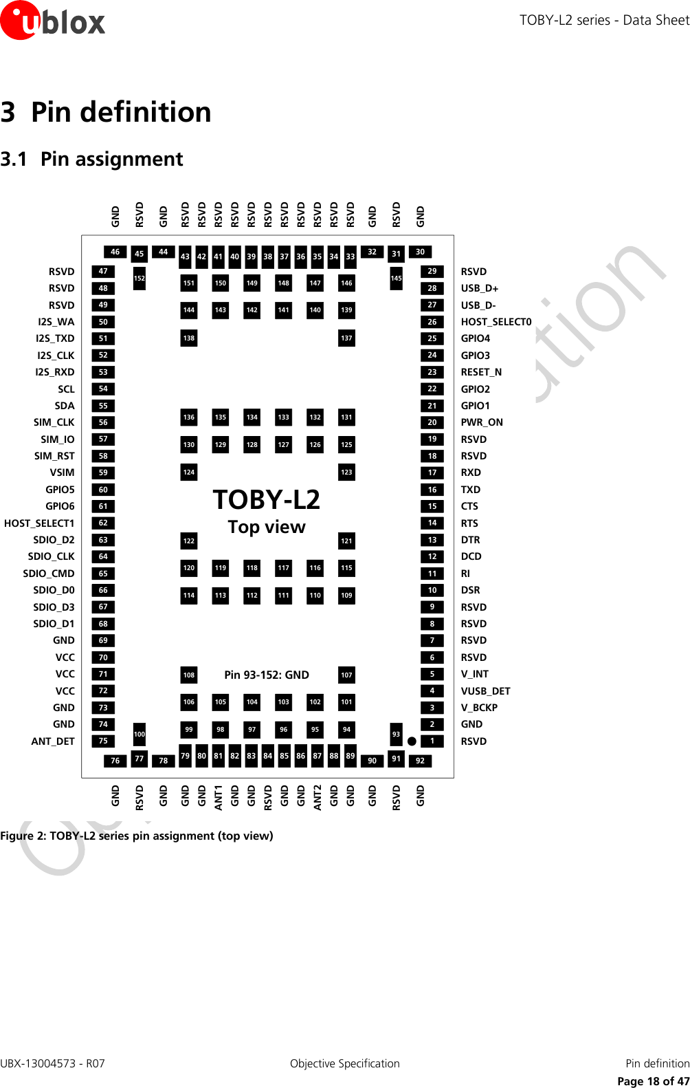
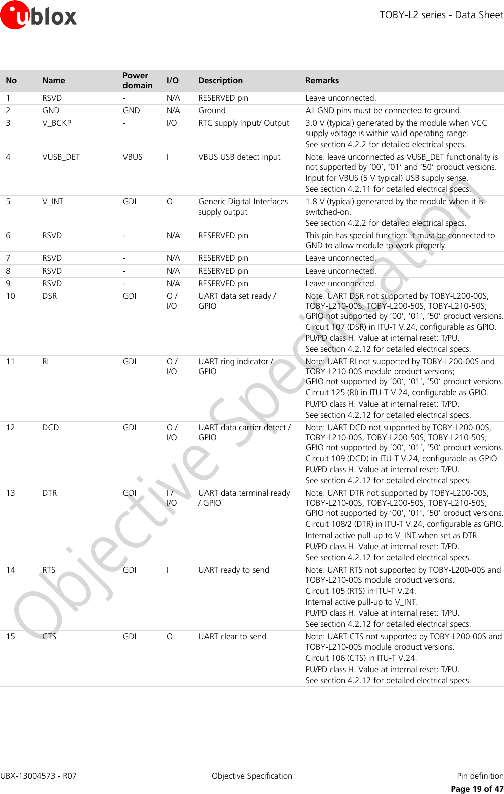
![TOBY-L2 series - Data Sheet UBX-13004573 - R07 Objective Specification Pin definition Page 20 of 47 No Name Power domain I/O Description Remarks 16 TXD GDI I UART data input Note: UART TXD not supported by TOBY-L200-00S and TOBY-L210-00S module product versions. Circuit 103 (TxD) in ITU-T V.24. Internal active pull-up to V_INT. PU/PD class M. Value at internal reset: T/PD. See section 4.2.12 for detailed electrical specs. 17 RXD GDI O UART data output Note: UART RXD not supported by TOBY-L200-00S and TOBY-L210-00S module product versions. Circuit 104 (RxD) in ITU-T V.24. PU/PD class M. Value at internal reset: T/PU. See section 4.2.12 for detailed electrical specs. 18 RSVD - N/A RESERVED pin Leave unconnected. 19 RSVD - N/A RESERVED pin Leave unconnected. 20 PWR_ON POS I Power-on input Internal active pull-up to VCC enabled. See section 4.2.8 for detailed electrical specs. 21 GPIO1 GDI I/O GPIO Note: not supported by ‘00’, ‘01’, ‘50’ product versions PU/PD class M. Value at internal reset: T/PD. See section 4.2.12 for detailed electrical specs. 22 GPIO2 GDI I/O GPIO Note: not supported by ‘00’, ‘01’, ‘50’ product versions PU/PD class M. Value at internal reset: T/PD. See section 4.2.12 for detailed electrical specs. 23 RESET_N ERS I External reset input Internal active pull-up to VCC enabled. See section 4.2.9 for detailed electrical specs. 24 GPIO3 GDI I/O GPIO Note: not supported by ‘00’, ‘01’, ‘50’ product versions PU/PD class M. Value at internal reset: T/PD. See section 4.2.12 for detailed electrical specs. 25 GPIO4 GDI I/O GPIO Note: not supported by ‘00’, ‘01’, ‘50’ product versions PU/PD class M. Value at internal reset: T/PD. See section 4.2.12 for detailed electrical specs. 26 HOST_SELECT0 GDI I Input for the selection of module configuration by the host processor Note: not supported by ‘00’, ‘01’, ‘50’ product versions PU/PD class M. Value at internal reset: T/PD. See section 4.2.12 for detailed electrical specs. 27 USB_D- USB I/O USB Data Line D- 90 nominal differential impedance Pull-up, pull-down and series resistors as required by the USB Revision 2.0 specification [18] are part of the USB pin driver and need not be provided externally. See section 4.2.11 for detailed electrical specs. 28 USB_D+ USB I/O USB Data Line D+ 90 nominal differential impedance Pull-up, pull-down and series resistors as required by the USB Revision 2.0 specification [18] are part of the USB pin driver and need not be provided externally. See section 4.2.11 for detailed electrical specs. 29 RSVD - N/A RESERVED pin Leave unconnected. 30 GND GND N/A Ground All GND pins must be connected to ground. 31 RSVD - N/A RESERVED pin Leave unconnected. 32 GND GND N/A Ground All GND pins must be connected to ground. 33 RSVD - N/A RESERVED pin Leave unconnected. 34 RSVD - N/A RESERVED pin Leave unconnected. 35 RSVD - N/A RESERVED pin Leave unconnected. 36 RSVD - N/A RESERVED pin Leave unconnected. 37 RSVD - N/A RESERVED pin Leave unconnected. 38 RSVD - N/A RESERVED pin Leave unconnected. 39 RSVD - N/A RESERVED pin Leave unconnected. 40 RSVD - N/A RESERVED pin Leave unconnected. 41 RSVD - N/A RESERVED pin Leave unconnected. 42 RSVD - N/A RESERVED pin Leave unconnected.](https://usermanual.wiki/u-blox/TOBYL201.Datasheet/User-Guide-2644987-Page-20.png)
![TOBY-L2 series - Data Sheet UBX-13004573 - R07 Objective Specification Pin definition Page 21 of 47 No Name Power domain I/O Description Remarks 43 RSVD - N/A RESERVED pin Leave unconnected. 44 GND GND N/A Ground All GND pins must be connected to ground. 45 RSVD - N/A RESERVED pin Leave unconnected. 46 GND GND N/A Ground All GND pins must be connected to ground. 47 RSVD - N/A RESERVED pin Leave unconnected. 48 RSVD - N/A RESERVED pin Leave unconnected. 49 RSVD - N/A RESERVED pin Leave unconnected. 50 I2S_WA GDI I/O / I/O I2S word alignment / GPIO Note: not supported by ‘00’, ‘01’, ‘50’ product versions I2S word alignment, otherwise configurable as GPIO. PU/PD class M. Value at internal reset: T/PD. See section 4.2.12 for detailed electrical specs. 51 I2S_TXD GDI O / I/O I2S transmit data / GPIO Note: not supported by ‘00’, ‘01’, ‘50’ product versions I2S transmit data out, otherwise configurable as GPIO. PU/PD class M. Value at internal reset: T/PD. See section 4.2.12 for detailed electrical specs. 52 I2S_CLK GDI I/O / I/O I2S clock / GPIO Note: not supported by ‘00’, ‘01’, ‘50’ product versions I2S serial clock, otherwise configurable as GPIO. PU/PD class M. Value at internal reset: T/PD. See section 4.2.12 for detailed electrical specs. 53 I2S_RXD GDI I / I/O I2S receive data / GPIO Note: not supported by ‘00’, ‘01’, ‘50’ product versions I2S receive data in, otherwise configurable as GPIO. PU/PD class M. Value at internal reset: T/PD. See section 4.2.12 for detailed electrical specs 54 SCL DDC O I2C bus clock line Note: not supported by ‘00’, ‘01’, ‘50’ product versions Fixed open drain. No internal pull-up. Value at internal reset: T. See section 4.2.13 for detailed electrical specs. 55 SDA DDC I/O I2C bus data line Note: not supported by ‘00’, ‘01’, ‘50’ product versions Fixed open drain. No internal pull-up. Value at internal reset: T. See section 4.2.13 for detailed electrical specs. 56 SIM_CLK SIM O SIM clock See section 4.2.10 for detailed electrical specs. 57 SIM_IO SIM I/O SIM data Internal 4.7 k pull-up resistor to VSIM. See section 4.2.10 for detailed electrical specs. 58 SIM_RST SIM O SIM reset See section 4.2.10 for detailed electrical specs. 59 VSIM - O SIM supply output VSIM = 1.8 V typical or 3.0 V typical generated by the module according to the SIM card/chip voltage type. See section 4.2.2 for detailed electrical specs. 60 GPIO5 GDI I/O GPIO Note: not supported by ‘00’, ‘01’, ‘50’ product versions PU/PD class M. Value at internal reset: T/PD. See section 4.2.12 for detailed electrical specs. 61 GPIO6 GDI I/O GPIO Note: not supported by ‘00’, ‘01’, ‘50’ product versions PU/PD class M. Value at internal reset: T/PD. See section 4.2.12 for detailed electrical specs. 62 HOST_SELECT1 GDI I Input for the selection of module configuration by the host processor Note: not supported by ‘00’, ‘01’, ‘50’ product versions PU/PD class M. Value at internal reset: T/PD. See section 4.2.12 for detailed electrical specs. 63 SDIO_D2 GDI I/O SDIO serial data [2] Note: not supported by ‘00’, ‘01’ product versions. PU/PD class M. Value at internal reset: T/PD. See section 4.2.12 for detailed electrical specs. 64 SDIO_CLK GDI O SDIO serial clock Note: not supported by ‘00’, ‘01’ product versions. PU/PD class M. Value at internal reset: T/PD. See section 4.2.12 for detailed electrical specs. 65 SDIO_CMD GDI I/O SDIO command Note: not supported by ‘00’, ‘01’ product versions. PU/PD class M. Value at internal reset: T/PD. See section 4.2.12 for detailed electrical specs.](https://usermanual.wiki/u-blox/TOBYL201.Datasheet/User-Guide-2644987-Page-21.png)
![TOBY-L2 series - Data Sheet UBX-13004573 - R07 Objective Specification Pin definition Page 22 of 47 No Name Power domain I/O Description Remarks 66 SDIO_D0 GDI I/O SDIO serial data [0] Note: not supported by ‘00’, ‘01’ product versions. PU/PD class M. Value at internal reset: T/PD. See section 4.2.12 for detailed electrical specs. 67 SDIO_D3 GDI I/O SDIO serial data [3] Note: not supported by ‘00’, ‘01’ product versions. PU/PD class M. Value at internal reset: T/PD. See section 4.2.12 for detailed electrical specs. 68 SDIO_D1 GDI I/O SDIO serial data [1] Note: not supported by ‘00’, ‘01’ product versions. PU/PD class M. Value at internal reset: T/PD. See section 4.2.12 for detailed electrical specs. 69 GND GND N/A Ground All GND pins must be connected to ground. 70 VCC VCC I Module supply input All VCC pins must be connected to external supply. See sections 4.2.2 / 4.2.3 for detailed electrical specs. 71 VCC VCC I Module supply input All VCC pins must be connected to external supply. See sections 4.2.2 / 4.2.3 for detailed electrical specs. 72 VCC VCC I Module supply input All VCC pins must be connected to external supply. See sections 4.2.2 / 4.2.3 for detailed electrical specs. 73 GND GND N/A Ground All GND pins must be connected to ground. 74 GND GND N/A Ground All GND pins must be connected to ground. 75 ANT_DET ADC I Antenna detection Note: not supported by ‘00’, ‘01’, ‘50’ product versions 76 GND GND N/A Ground All GND pins must be connected to ground. 77 RSVD - N/A RESERVED pin Leave unconnected. 78 GND GND N/A Ground All GND pins must be connected to ground. 79 GND GND N/A Ground All GND pins must be connected to ground. 80 GND GND N/A Ground All GND pins must be connected to ground. 81 ANT1 ANT I/O Primary antenna 50 nominal characteristic impedance. Main Tx / Rx antenna interface. See section 4.2.4 / 4.2.5 / 4.2.6 for details. 82 GND GND N/A Ground All GND pins must be connected to ground. 83 GND GND N/A Ground All GND pins must be connected to ground. 84 RSVD - N/A RESERVED pin Leave unconnected. 85 GND GND N/A Ground All GND pins must be connected to ground. 86 GND GND N/A Ground All GND pins must be connected to ground. 87 ANT2 ANT I Secondary antenna 50 nominal characteristic impedance Rx only for Down-Link MIMO 2x2 and Rx diversity. See section 4.2.4 / 4.2.5 / 4.2.6 for details. 88 GND GND N/A Ground All GND pins must be connected to ground. 89 GND GND N/A Ground All GND pins must be connected to ground. 90 GND GND N/A Ground All GND pins must be connected to ground. 91 RSVD - N/A RESERVED pin Leave unconnected. 92 GND GND N/A Ground All GND pins must be connected to ground. 93-152 GND GND N/A Ground All GND pins must be connected to ground. Table 5: TOBY-L2 series pin-out For more information about the pin-out, see the TOBY-L2 / MPCI-L2 series System Integration Manual [2]. See Appendix A for an explanation of abbreviations and terms used.](https://usermanual.wiki/u-blox/TOBYL201.Datasheet/User-Guide-2644987-Page-22.png)
![TOBY-L2 series - Data Sheet UBX-13004573 - R07 Objective Specification Electrical specifications Page 27 of 47 4.2.4 LTE RF characteristics The LTE bands supported by each TOBY-L2 series module are defined in Table 2, while the following Table 12 describes the Transmitting and Receiving frequencies for each LTE band according to 3GPP TS 36.521-1 [14]. Parameter Min. Max. Unit Remarks Frequency range Band 17 (700 MHz) Uplink 704 716 MHz Module transmit Downlink 734 746 MHz Module receive Frequency range Band 13 (750 MHz) Uplink 777 787 MHz Module transmit Downlink 746 756 MHz Module receive Frequency range Band 28 (750 MHz) Uplink 703 748 MHz Module transmit Downlink 758 803 MHz Module receive Frequency range Band 20 (800 MHz) Uplink 832 862 MHz Module transmit Downlink 791 821 MHz Module receive Frequency range Band 5 (850 MHz) Uplink 824 849 MHz Module transmit Downlink 869 894 MHz Module receive Frequency range Band 8 (900 MHz) Uplink 880 915 MHz Module transmit Downlink 925 960 MHz Module receive Frequency range Band 4 (1700 MHz) Uplink 1710 1755 MHz Module transmit Downlink 2110 2155 MHz Module receive Frequency range Band 3 (1800 MHz) Uplink 1710 1785 MHz Module transmit Downlink 1805 1880 MHz Module receive Frequency range Band 2 (1900 MHz) Uplink 1850 1910 MHz Module transmit Downlink 1930 1990 MHz Module receive Frequency range Band 1 (2100 MHz) Uplink 1920 1980 MHz Module transmit Downlink 2110 2170 MHz Module receive Frequency range Band 7 (2600 MHz) Uplink 2500 2570 MHz Module transmit Downlink 2620 2690 MHz Module receive Table 12: LTE operating RF frequency bands TOBY-L2 series modules include a UE Power Class 3 LTE transmitter (see Table 2), with output power and characteristics according to 3GPP TS 36.521-1 [14]. TOBY-L2 series modules LTE receiver characteristics are compliant to 3GPP TS 36.521-1 [14], with LTE conducted receiver sensitivity performance described in Table 13.](https://usermanual.wiki/u-blox/TOBYL201.Datasheet/User-Guide-2644987-Page-27.png)
![TOBY-L2 series - Data Sheet UBX-13004573 - R07 Objective Specification Electrical specifications Page 28 of 47 Parameter Min. Typical Max. Unit Remarks Receiver input sensitivity Band 17 (700 MHz) –103.5 dBm Channel bandwidth = 5 MHz –100.5 dBm Channel bandwidth = 10 MHz Receiver input sensitivity Band 20 (800 MHz) –103.0 dBm Channel bandwidth = 5 MHz –97.0 dBm Channel bandwidth = 20 MHz Receiver input sensitivity Band 5 (850 MHz) –109.0 dBm Channel bandwidth = 1.4 MHz –103.0 dBm Channel bandwidth = 5 MHz –100.5 dBm Channel bandwidth = 10 MHz Receiver input sensitivity Band 8 (900 MHz) –110.0 dBm Channel bandwidth = 1.4 MHz –104.5 dBm Channel bandwidth = 5 MHz –101.5 dBm Channel bandwidth = 10 MHz Receiver input sensitivity Band 4 (1700 MHz) –109.5 dBm Channel bandwidth = 1.4 MHz –103.5 dBm Channel bandwidth = 5 MHz –98.0 dBm Channel bandwidth = 20 MHz Receiver input sensitivity Band 3 (1800 MHz) –110.0 dBm Channel bandwidth = 1.4 MHz –104.5 dBm Channel bandwidth = 5 MHz –98.5 dBm Channel bandwidth = 20 MHz Receiver input sensitivity Band 2 (1900 MHz) –110.0 dBm Channel bandwidth = 1.4 MHz –104.0 dBm Channel bandwidth = 5 MHz –98.0 dBm Channel bandwidth = 20 MHz Receiver input sensitivity Band 1 (2100 MHz) –104.5 dBm Channel bandwidth = 5 MHz –98.5 dBm Channel bandwidth = 20 MHz Receiver input sensitivity Band 7 (2600 MHz) –102.5 dBm Channel bandwidth = 5 MHz –97.0 dBm Channel bandwidth = 20 MHz Condition: 50 source, Throughput > 95%, dual receiver, QPSK modulation, Other settings as per 3GPP TS 36.521-1 [14] Table 13: LTE receiver sensitivity performance](https://usermanual.wiki/u-blox/TOBYL201.Datasheet/User-Guide-2644987-Page-28.png)
![TOBY-L2 series - Data Sheet UBX-13004573 - R07 Objective Specification Electrical specifications Page 29 of 47 4.2.5 3G RF characteristics The 3G bands supported by each TOBY-L2 series module are defined in Table 2, while the following Table 14 describes the Transmitting and Receiving frequencies for each 3G band according to 3GPP TS 34.121-1 [15]. Parameter Min. Max. Unit Remarks Frequency range Band 5 (850 MHz) Uplink 824 849 MHz Module transmit Downlink 869 894 MHz Module receive Frequency range Band 8 (900 MHz) Uplink 880 915 MHz Module transmit Downlink 925 960 MHz Module receive Frequency range Band 4 (AWS, 1700 MHz) Uplink 1710 1755 MHz Module transmit Downlink 2110 2155 MHz Module receive Frequency range Band 2 (1900 MHz) Uplink 1850 1910 MHz Module transmit Downlink 1930 1990 MHz Module receive Frequency range Band 1 (2100 MHz) Uplink 1920 1980 MHz Module transmit Downlink 2110 2170 MHz Module receive Table 14: 3G operating RF frequency bands TOBY-L2 series modules include a UE Power Class 3 3G transmitter (see Table 2), with output power and characteristics according to 3GPP TS 34.121-1 [15]. TOBY-L2 series modules 3G receiver characteristics are compliant to 3GPP TS 34.121-1 [15], with 3G conducted receiver sensitivity performance described in Table 15. Parameter Min. Typical Max. Unit Remarks Receiver input sensitivity Band 5 (850 MHz) –112.0 dBm Downlink RF level for RMC @ BER < 0.1 % Receiver input sensitivity Band 8 (900 MHz) –112.0 dBm Downlink RF level for RMC @ BER < 0.1 % Receiver input sensitivity Band 4 (AWS, 1700 MHz) –111.0 dBm Downlink RF level for RMC @ BER < 0.1 % Receiver input sensitivity Band 2 (1900 MHz) –111.0 dBm Downlink RF level for RMC @ BER < 0.1 % Receiver input sensitivity Band 1 (2100 MHz) –111.0 dBm Downlink RF level for RMC @ BER < 0.1 % Condition: 50 source, other settings as per 3GPP TS 34.121-1 [15] Table 15: 3G receiver sensitivity performance](https://usermanual.wiki/u-blox/TOBYL201.Datasheet/User-Guide-2644987-Page-29.png)
![TOBY-L2 series - Data Sheet UBX-13004573 - R07 Objective Specification Electrical specifications Page 30 of 47 4.2.6 2G RF characteristics The 2G bands supported by each TOBY-L2 series module are defined in Table 2, while the following Table 16 describes the Transmitting and Receiving frequencies for each 2G band according to 3GPP TS 51.010-1 [16]. Parameter Min. Max. Unit Remarks Frequency range GSM 850 Uplink 824 849 MHz Module transmit Downlink 869 894 MHz Module receive Frequency range E-GSM 900 Uplink 880 915 MHz Module transmit Downlink 925 960 MHz Module receive Frequency range DCS 1800 Uplink 1710 1785 MHz Module transmit Downlink 1805 1880 MHz Module receive Frequency range PCS 1900 Uplink 1850 1910 MHz Module transmit Downlink 1930 1990 MHz Module receive Table 16: 2G operating RF frequency bands TOBY-L2 series modules include a GMSK Power Class 4 transmitter for GSM/E-GSM bands, GMSK Power Class 1 transmitter for DCS/PCS bands, 8-PSK Power Class E2 transmitter for all 2G bands (see Table 2), with output power and characteristics according to 3GPP TS 51.010-1 [16]. TOBY-L2 series modules 2G receiver characteristics are compliant to 3GPP TS 51.010-1 [16], with conducted receiver sensitivity performance described in Table 17. Parameter Min. Typical Max. Unit Remarks Receiver input sensitivity GSM 850 / E-GSM 900 –110.0 dBm Downlink RF level @ BER Class II < 2.4 % Receiver input sensitivity DCS 1800 / PCS 1900 –109.0 dBm Downlink RF level @ BER Class II < 2.4 % Condition: 50 source, other settings as per 3GPP TS 51.010-1 [16] Table 17: 2G receiver sensitivity performance 4.2.7 ANT_DET pin Antenna detection (ANT_DET) is not supported by “00”, “01” and “50” product versions. Pin Name Parameter Min. Typical Max. Unit Remarks ANT_DET Output DC current pulse value 26 µA Generated by means of the AT+UANTR command Output DC current pulse time length 3.6 ms Generated by means of the AT+UANTR command Table 18: ANT_DET pin characteristics](https://usermanual.wiki/u-blox/TOBYL201.Datasheet/User-Guide-2644987-Page-30.png)
![TOBY-L2 series - Data Sheet UBX-13004573 - R07 Objective Specification Electrical specifications Page 32 of 47 4.2.10 SIM pins The SIM pins are a dedicated interface to the external SIM card/chip. The electrical characteristics fulfill regulatory specification requirements. The values in Table 21 are for information only. Parameter Min. Typical Max. Unit Remarks Low-level input –0.30 0.63 V VSIM = 1.8 V –0.30 0.80 V VSIM = 3.0 V High-level input 1.17 2.10 V VSIM = 1.8 V 2.00 3.30 V VSIM = 3.0 V Low-level output 0.00 0.45 V VSIM = 1.8 V, Max value at IOL = +2.0 mA 0.00 0.40 V VSIM = 3.0 V, Max value at IOL = +2.0 mA High-level output 1.35 1.80 V VSIM = 1.8 V, Min value at IOH = –2.0 mA 2.60 2.90 V VSIM = 3.0 V, Min value at IOH = –2.0 mA Input / Output leakage current –500 500 nA 0 V < VIN < 0.63 V or 1.17 V < VIN < 2.10 V 0 V < VIN < 0.80 V or 2.00 V < VIN < 3.30 V Clock frequency on SIM_CLK 3.25 MHz Internal pull-up resistor on SIM_IO 4.7 k Internal pull-up to VSIM supply Table 21: SIM pins characteristics 4.2.11 USB pins USB data lines (USB_D+ / USB_D–) are compliant to the USB 2.0 high-speed specification. See the Universal Serial Bus Revision 2.0 specification [18] for detailed electrical characteristics. Parameter Min. Typical Max. Unit Remarks VUSB_DET pin, High-level input 4.40 5.00 5.25 V VUSB_DET pin, Low-level input 0.00 1.30 V VUSB_DET pin, Current sink 100 µA High-speed squelch detection threshold (input differential signal amplitude) 100 150 mV High speed disconnect detection threshold (input differential signal amplitude) 525 625 mV High-speed data signaling input common mode voltage range –50 500 mV High-speed idle output level –10 10 mV High-speed data signaling output high level 360 440 mV High-speed data signaling output low level –10 10 mV Chirp J level (output differential voltage) 700 1100 mV Chirp K level (output differential voltage) –900 –500 mV Table 22: USB pins characteristics](https://usermanual.wiki/u-blox/TOBYL201.Datasheet/User-Guide-2644987-Page-32.png)
![TOBY-L2 series - Data Sheet UBX-13004573 - R07 Objective Specification Electrical specifications Page 33 of 47 4.2.12 Generic Digital Interfaces pins Parameter Min Typical Max Unit Remarks Internal supply for GDI domain 1.80 V Digital I/O Interfaces supply (V_INT) Low-level input –0.30 0.63 V High-level input 1.17 2.10 V Low-level output 0.00 0.45 V Max value at IOL = +2.0 mA High-level output 1.35 1.80 V Min value at IOH = –2.0 mA Input/output leakage current –500 500 nA 0 V < VIN < 0.63 V or 1.17 V < VIN < 2.10 V Internal active pull-up resistance 30 130 k Pull-Up class H 30 180 k Pull-Up class M Internal active pull-down resistance 30 150 k Pull-Down class H 30 180 k Pull-Down class M Table 23: GDI pin characteristics 4.2.13 DDC (I2C) pins The DDC (I2C) interface is not supported by “00”, “01” and “50” product versions. DDC (I2C) lines (SCL and SDA) are compliant to the I2C-bus standard mode specification. See the I2C-Bus Specification [19] for detailed electrical characteristics. Parameter Min Typical Max Unit Remarks Internal supply for GDI domain 1.80 V Digital I/O Interfaces supply (V_INT) Low-level input –0.30 0.63 V High-level input 1.17 2.10 V Low-level output 0.00 0.45 V Max value at IOL = +2.0 mA Input/output leakage current –500 500 nA 0 V < VIN < 0.63 V or 1.17 V < VIN < 2.10 V Clock frequency on SCL 100 kHz Table 24: DDC (I2C) pins characteristics](https://usermanual.wiki/u-blox/TOBYL201.Datasheet/User-Guide-2644987-Page-33.png)
![TOBY-L2 series - Data Sheet UBX-13004573 - R07 Objective Specification Electrical specifications Page 34 of 47 4.3 Parameters for ATEX applications This section provides useful parameters and information to integrate TOBY-L2 series modules in applications intended for use in areas with potentially explosive atmospheres (ATEX), describing: Total internal capacitance and inductance of TOBY-L2 series modules (see Table 25) Maximum RF output power and voltage at the antenna pin of TOBY-L2 series modules (see Table 26) Any specific applicable requirement for the implementation of the apparatus integrating TOBY-L2 series modules, intended for use in potentially explosive atmospheres, must be fulfilled according to the exact applicable standards: check the detailed requisites on the pertinent normative for the application, as for example the IEC 60079-0 [20], IEC 60079-11 [21], IEC 60079-26 [22] standards. The certification of the application device that integrates a TOBY-L2 series module and the compliance of the application device with all the applicable certification schemes, directives and standards required for use in potentially explosive atmospheres are the sole responsibility of the application device manufacturer. Table 25 describes the maximum total internal capacitance and the maximum total internal inductance, considering internal parts tolerance, provided by TOBY-L2 series modules. Module Parameter Description Value Unit TOBY-L200, TOBY-L201 Ci Maximum total internal capacitance 267 µF Li Maximum total internal inductance 12.8 µH TOBY-L210, TOBY-L280 Ci Maximum total internal capacitance 267 µF Li Maximum total internal inductance 12.9 µH Table 25: TOBY-L2 series maximum total internal capacitance and maximum total internal inductance Table 26 describes the maximum RF output power transmitted by TOBY-L2 series modules from the primary antenna (ANT1) pin as Power Class 4 Mobile Stations for GSM 850 / E-GSM 900 bands, and the corresponding maximum voltage into a 50 system load. Module Parameter Description Value Unit All ANT1 Pout Maximum RF output power from ANT1 pin 35.0 dBm ANT1 Vout on 50 Maximum voltage from ANT1 pin into a 50 system load 12.6 Vrms Table 26: TOBY-L2 series maximum RF output power and corresponding maximum voltage into a 50 load The TOBY-L2 series modules do not contain internal blocks which increase the input voltage (e.g. like step-up, duplicators, boosters, etc.) except for the primary antenna (ANT1) pin which maximum RF output power and corresponding maximum voltage into a 50 system is illustrated in Table 26.](https://usermanual.wiki/u-blox/TOBYL201.Datasheet/User-Guide-2644987-Page-34.png)
![TOBY-L2 series - Data Sheet UBX-13004573 - R07 Objective Specification Mechanical specifications Page 35 of 47 5 Mechanical specifications CIAGH1 J1D FKM1 M1 M2 P2BGH1J1H2J2J2 H2ANT1 pinOOLNH2J2J2 H2ANT2 pinM1 M1 M3IIIOH1J1J1J1EP3FP1H1IOPin 1 Indicator Figure 3: TOBY-L2 series dimensions (Bottom and Sides views) Parameter Description Typical Tolerance A Module Height [mm] 35.6 (1401.6 mil) +0.20/–0.20 (+7.9/–7.9 mil) B Module Width [mm] 24.8 (976.4 mil) +0.20/–0.20 (+7.9/–7.9 mil) C Module Thickness [mm] 2.6 (102.4 mil) +0.27/–0.17 (+10.6/–6.7 mil) D Horizontal Edge to Lateral Pin Pitch [mm] 2.4 (94.5 mil) +0.20/–0.20 (+7.9/–7.9 mil) E Vertical Edge to Lateral Pin Pitch [mm] 2.25 (88.6 mil) +0.20/–0.20 (+7.9/–7.9 mil) F Edge to Lateral Pin Pitch [mm] 1.45 (57.1 mil) +0.20/–0.20 (+7.9/–7.9 mil) G Lateral Pin to Pin Pitch [mm] 1.1 (43.3 mil) +0.02/–0.02 (+0.8/–0.8 mil) H1 Lateral Pin Height [mm] 0.8 (31.5 mil) +0.02/–0.02 (+0.8/–0.8 mil) H2 Lateral Pin close to ANT1 and ANT2 Height [mm] 0.9 (35.4 mil) +0.02/–0.02 (+0.8/–0.8 mil) I Lateral Pin Width [mm] 1.5 (59.1 mil) +0.02/–0.02 (+0.8/–0.8 mil) J1 Lateral Pin to Pin Distance [mm] 0.3 (11.8 mil) +0.02/–0.02 (+0.8/–0.8 mil) J2 Lateral Pin to Pin close to ANT Distance [mm] 0.2 (7.9 mil) +0.02/–0.02 (+0.8/–0.8 mil) K Horizontal Edge to Central Pin Pitch [mm] 3.15 (124.0 mil) +0.20/–0.20 (+7.9/–7.9 mil) L Vertical Edge to Central Pin Pitch [mm] 7.15 (281.5 mil) +0.20/–0.20 (+7.9/–7.9 mil) M1 Central Pin to Pin Horizontal Pitch [mm] 1.8 (70.9 mil) +0.02/–0.02 (+0.8/–0.8 mil) M2 Central Pin to Pin Horizontal Pitch [mm] 5.2 (204.7 mil) +0.02/–0.02 (+0.8/–0.8 mil) M3 Central Pin to Pin Horizontal Pitch [mm] 4.5 (177.2 mil) +0.02/–0.02 (+0.8/–0.8 mil) N Central Pin to Pin Vertical Pitch [mm] 2.1 (82.7 mil) +0.02/–0.02 (+0.8/–0.8 mil) O Central Pin Height and Width [mm] 1.1 (43.3 mil) +0.02/–0.02 (+0.8/–0.8 mil) P1 Horizontal Edge to Corner Pin Pitch [mm] 1.1 (43.3 mil) +0.20/–0.20 (+7.9/–7.9 mil) P2 Horizontal Edge to Corner Pin Pitch [mm] 1.25 (49.2 mil) +0.20/–0.20 (+7.9/–7.9 mil) P3 Horizontal Edge to Corner Pin Pitch [mm] 2.85 (112.2 mil) +0.20/–0.20 (+7.9/–7.9 mil) Weight Module Weight [g] < 7 Table 27: TOBY-L2 series dimensions](https://usermanual.wiki/u-blox/TOBYL201.Datasheet/User-Guide-2644987-Page-35.png)
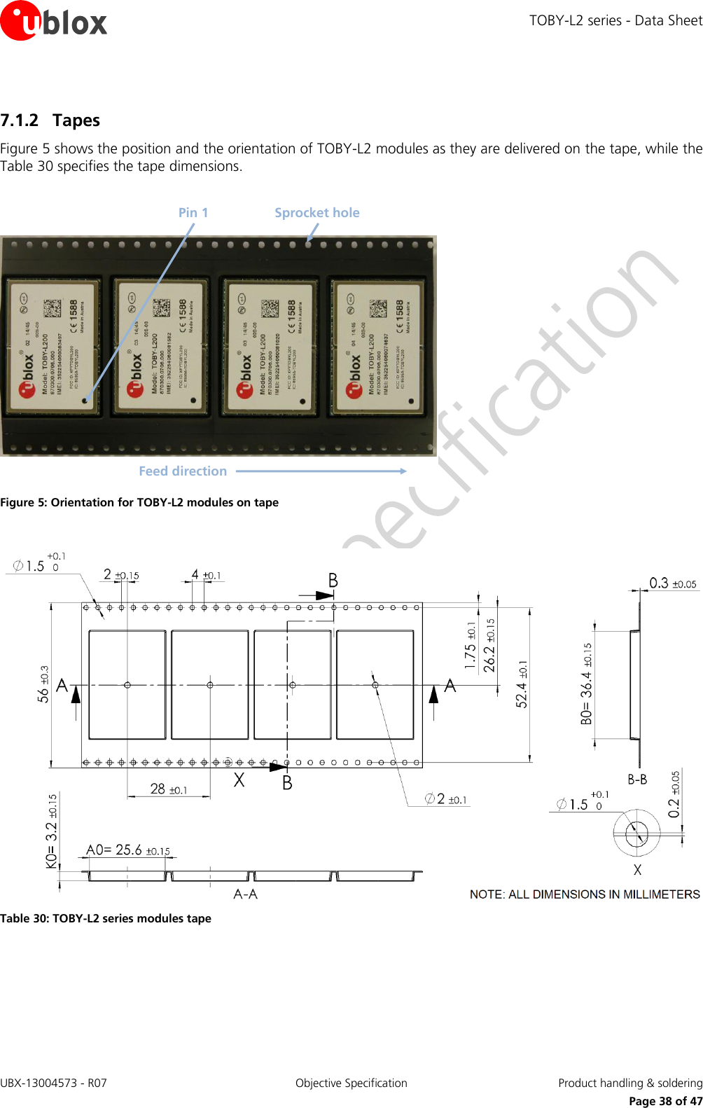
![TOBY-L2 series - Data Sheet UBX-13004573 - R07 Objective Specification Product handling & soldering Page 37 of 47 7 Product handling & soldering 7.1 Packaging TOBY-L2 series modules are delivered as hermetically sealed, reeled tapes to enable efficient production, production lot set-up and tear-down. For more information about packaging, see the u-blox Package Information User Guide [9]. 7.1.1 Reels TOBY-L2 series modules are deliverable in quantities of 150 pieces on a reel. The modules are delivered using the reel Type B described in the Figure 4 and in the u-blox Package Information Guide [9]. Figure 4: TOBY-L2 series modules reel Parameter Specification Reel Type B Delivery Quantity 150 Table 29: Reel information for TOBY-L2 series modules Quantities of less than 150 pieces are also available. Contact u-blox for more information.](https://usermanual.wiki/u-blox/TOBYL201.Datasheet/User-Guide-2644987-Page-37.png)
![TOBY-L2 series - Data Sheet UBX-13004573 - R07 Objective Specification Product handling & soldering Page 39 of 47 7.2 Moisture Sensitivity Levels TOBY-L2 series modules are Moisture Sensitive Devices (MSD) in accordance to the IPC/JEDEC specification. The Moisture Sensitivity Level (MSL) relates to the packaging and handling precautions required. TOBY-L2 series modules are rated at MSL level 4. For more information regarding moisture sensitivity levels, labeling, storage and drying see the u-blox Package Information Guide [9]. For MSL standard see IPC/JEDEC J-STD-020 (can be downloaded from www.jedec.org). 7.3 Reflow soldering Reflow profiles are to be selected according to u-blox recommendations (see TOBY-L2 / MPCI-L2 series System Integration Manual [2]). Failure to observe these recommendations can result in severe damage to the device! 7.4 ESD precautions TOBY-L2 series modules contain highly sensitive electronic circuitry and are Electrostatic Sensitive Devices (ESD). Handling TOBY-L2 series modules without proper ESD protection may destroy or damage them permanently. TOBY-L2 series modules are Electrostatic Sensitive Devices (ESD) and require special ESD precautions typically applied to ESD sensitive components. Table 7 reports the maximum ESD ratings of the TOBY-L2 series modules. Proper ESD handling and packaging procedures must be applied throughout the processing, handling and operation of any application that incorporates TOBY-L2 series module. ESD precautions should be implemented on the application board where the module is mounted, as described in the TOBY-L2 / MPCI-L2 series System Integration Manual [2]. Failure to observe these recommendations can result in severe damage to the device!](https://usermanual.wiki/u-blox/TOBYL201.Datasheet/User-Guide-2644987-Page-39.png)
![TOBY-L2 series - Data Sheet UBX-13004573 - R07 Objective Specification Default settings Page 40 of 47 8 Default settings Item AT Settings Comments USB interface Enabled TOBY-L2 series modules provide by default the following set of USB functions: CDC-ACM for AT command and data RNDIS for Ethernet-over-USB connection The USB can be configured by the AT+UUSBCONF command to select different sets of USB functions available in mutually exclusive way, configuring the active USB profile consisting of a specific set of functions with various capabilities and purposes (for more details, see the TOBY-L2 / MPCI-L2 series System Integration Manual [2] and the u-blox AT Commands Manual [1], +UUSBCONF AT command). Power Saving AT+UPSV=0 Disabled Network registration AT+COPS=0 Self network registration Table 31: Default settings](https://usermanual.wiki/u-blox/TOBYL201.Datasheet/User-Guide-2644987-Page-40.png)
![TOBY-L2 series - Data Sheet UBX-13004573 - R07 Objective Specification Labeling and ordering information Page 42 of 47 Code Meaning Example TOBY Form factor TOBY TG Platform (Technology and Generation) Technology: G:GSM; U: HSUPA; L:LTE, C:CDMA 1xRTT; D:EV-DO Generation: 1…9 L2 VV Variant function set based on the same platform [00…99] 00 TT Major product version [00…99] 00 Q Quality grade S = professional A = automotive S XX Minor product version (not relevant for certification) Default value is 00 Table 33: Part identification code 9.3 Ordering information Ordering No. Product TOBY-L200-00S LTE bands 2 / 4 / 5 / 7 / 17, DC-HSPA+ bands 1 / 2 / 4 / 5 / 8, (E)GPRS bands 850 / 900 / 1800 / 1900 module, mainly designed for operation in America, 35.6 x 24.8 x 2.6 mm, 150 pcs/reel TOBY-L200-50S LTE bands 2 / 4 / 5 / 7 / 17, DC-HSPA+ bands 1 / 2 / 4 / 5 / 8, (E)GPRS bands 850 / 900 / 1800 / 1900 module, mainly designed for operation in America, supporting UART and SDIO interfaces, 35.6 x 24.8 x 2.6 mm, 150 pcs/reel TOBY-L201-01S LTE bands 2 / 4 / 5 / 13 / 17, DC-HSPA+ bands 2 / 5 module, mainly designed for operation in America, supporting UART and embedded TCP/UDP, HTTP/FTP, 35.6 x 24.8 x 2.6 mm, 150 pcs/reel TOBY-L210-00S LTE bands 1 / 3 / 5 / 7 / 8 / 20, DC-HSPA+ bands 1 / 2 / 5 / 8, (E)GPRS bands 850 / 900 / 1800 / 1900 module, mainly designed for operation in Europe, Asia and other countries, 35.6 x 24.8 x 2.6 mm, 150 pcs/reel TOBY-L210-50S LTE bands 1 / 3 / 5 / 7 / 8 / 20, DC-HSPA+ bands 1 / 2 / 5 / 8, (E)GPRS bands 850 / 900 / 1800 / 1900 module, mainly designed for operation in Europe, Asia and other countries, supporting UART and SDIO interfaces, 35.6 x 24.8 x 2.6 mm, 150 pcs/reel TOBY-L280-00S LTE bands 1 / 3 / 5 / 7 / 8 / 28, DC-HSPA+ bands 1 / 2 / 5 / 8, (E)GPRS bands 850 / 900 / 1800 / 1900 module, mainly designed for operation in South East-Asia and Oceania, supporting UART, 35.6 x 24.8 x 2.6 mm, 150 pcs/reel Table 34: Product ordering codes](https://usermanual.wiki/u-blox/TOBYL201.Datasheet/User-Guide-2644987-Page-42.png)
![TOBY-L2 series - Data Sheet UBX-13004573 - R07 Objective Specification Related documents Page 45 of 47 Related documents [1] u-blox AT Commands Manual, Docu No UBX-13002752 [2] u-blox TOBY-L2 / MPCI-L2 series System Integration Manual, Docu No UBX-13004618 [3] u-blox Android RIL Production delivery Application note, Docu No UBX-13002041 [4] u-blox Windows Embedded RIL Production delivery Application note, Docu No UBX-13002043 [5] u-blox GNSS Implementation Application Note, Docu No UBX-13001849 [6] u-blox Mux Implementation Application Note, Docu No UBX-13001887 [7] u-blox GNSS Implementation Application Note, Docu No UBX-13001849 [8] u-blox Wi-Fi / Cellular Integration Application Note, Docu No UBX-14003264 [9] u-blox Package Information User Guide, Docu No UBX-14001652 [10] 3GPP TS 27.007 - AT command set for User Equipment (UE) [11] 3GPP TS 27.005 - Use of Data Terminal Equipment - Data Circuit terminating Equipment (DTE - DCE) interface for Short Message Service (SMS) and Cell Broadcast Service (CBS) [12] 3GPP TS 27.010 - Terminal Equipment to User Equipment (TE-UE) multiplexer protocol [13] 3GPP TS 26.267 - Technical Specification Group Services and System Aspects; eCall Data Transfer; In-band modem solution; General description [14] 3GPP TS 36.521-1 - Evolved Universal Terrestrial Radio Access; User Equipment conformance specification; Radio transmission and reception; Part 1: Conformance Testing [15] 3GPP TS 34.121-1 - User Equipment conformance specification; Radio transmission and reception (FDD); Part 1: Conformance specification [16] 3GPP TS 51.010-1 - Mobile Station conformance specification; Part 1: Conformance specification [17] ITU-T Recommendation V24, 02-2000. List of definitions for interchange circuits between Data Terminal Equipment (DTE) and Data Connection Equipment (DCE) [18] Universal Serial Bus Revision 2.0 specification, http://www.usb.org/developers/docs/usb20_docs/ [19] I2C-bus specification and user manual - Rev. 5 - 9 October 2012 - NXP Semiconductors, http://www.nxp.com/documents/user_manual/UM10204.pdf [20] IEC 60079-0 - Explosive atmospheres, Part 0: Equipment general requirements [21] IEC 60079-11 - Explosive atmospheres, Part 11: Equipment protection by intrinsic safety 'i' [22] IEC 60079-26 - Explosive atmospheres, Part 26: Equipment with EPL Ga For regular updates to u-blox documentation and to receive product change notifications please register on our homepage (www.u-blox.com).](https://usermanual.wiki/u-blox/TOBYL201.Datasheet/User-Guide-2644987-Page-45.png)