u blox TOBYL280 GSM/UMTS/LTE Data Module User Manual TOBY L2 series
u-blox AG GSM/UMTS/LTE Data Module TOBY L2 series
u blox >
Contents
- 1. System Integrators Manual
- 2. TempConfidential_TOBY-L2-MPCI-L2_SysIntegrManual_UBX-13004618
System Integrators Manual
![TOBY-L2 and MPCI-L2 series - System Integration Manual UBX-13004618 - R08 Early Production Information System description Page 13 of 158 Function Pin Name Pin No I/O Description Remarks SIM VSIM 59 O SIM supply output VSIM = 1.8 V / 3 V output as per the connected SIM type. See section 1.8 for functional description. See section 2.5 for external circuit design-in. SIM_IO 57 I/O SIM data Data input/output for 1.8 V / 3 V SIM Internal 4.7 k pull-up to VSIM. See section 1.8 for functional description. See section 2.5 for external circuit design-in. SIM_CLK 56 O SIM clock 3.25 MHz clock output for 1.8 V / 3 V SIM See section 1.8 for functional description. See section 2.5 for external circuit design-in. SIM_RST 58 O SIM reset Reset output for 1.8 V / 3 V SIM See section 1.8 for functional description. See section 2.5 for external circuit design-in. USB VUSB_DET 4 I USB detect input Note: leave unconnected, as VBUS detect is not supported. Input for VBUS (5 V typical) USB supply sense. See section 1.9.1 for functional description. See section 2.6.1 for external circuit design-in. USB_D- 27 I/O USB Data Line D- USB interface for AT commands, data communication, FOAT, FW update by u-blox EasyFlash tool and diagnostic. 90 nominal differential impedance (Z0) 30 nominal common mode impedance (ZCM) Pull-up or pull-down resistors and external series resistors as required by the USB 2.0 specifications [4] are part of the USB pad driver and need not be provided externally. See section 1.9.1 for functional description. See section 2.6.1 for external circuit design-in. USB_D+ 28 I/O USB Data Line D+ USB interface for AT commands, data communication, FOAT, FW update by u-blox EasyFlash tool and diagnostic. 90 nominal differential impedance (Z0) 30 nominal common mode impedance (ZCM) Pull-up or pull-down resistors and external series resistors as required by the USB 2.0 specifications [4] are part of the USB pad driver and need not be provided externally. See section 1.9.1 for functional description. See section 2.6.1 for external circuit design-in.](https://usermanual.wiki/u-blox/TOBYL280.System-Integrators-Manual/User-Guide-2664029-Page-13.png)
![TOBY-L2 and MPCI-L2 series - System Integration Manual UBX-13004618 - R08 Early Production Information System description Page 15 of 158 Function Pin Name Pin No I/O Description Remarks DDC SCL 54 O I2C bus clock line Note: not supported by “00”, “01”, “50” product versions. 1.8 V open drain, for communication with u-blox GNSS receivers and other I2C-slave devices as an audio codec. External pull-up required. See section 1.9.3 for functional description. See section 2.6.3 for external circuit design-in. SDA 55 I/O I2C bus data line Note: not supported by “00”, “01”, “50” product versions. 1.8 V open drain, for communication with u-blox GNSS receivers and other I2C-slave devices as an audio codec. External pull-up required. See section 1.9.3 for functional description. See section 2.6.3 for external circuit design-in. SDIO SDIO_D0 66 I/O SDIO serial data [0] Note: not supported by “00”, “01” product versions. SDIO interface for communication with external Wi-Fi chip See section 1.9.4 for functional description. See section 2.6.4 for external circuit design-in. SDIO_D1 68 I/O SDIO serial data [1] Note: not supported by “00”, “01” product versions. SDIO interface for communication with external Wi-Fi chip See section 1.9.4 for functional description. See section 2.6.4 for external circuit design-in. SDIO_D2 63 I/O SDIO serial data [2] Note: not supported by “00”, “01” product versions. SDIO interface for communication with external Wi-Fi chip See section 1.9.4 for functional description. See section 2.6.4 for external circuit design-in. SDIO_D3 67 I/O SDIO serial data [3] Note: not supported by “00”, “01” product versions. SDIO interface for communication with external Wi-Fi chip See section 1.9.4 for functional description. See section 2.6.4 for external circuit design-in. SDIO_CLK 64 O SDIO serial clock Note: not supported by “00”, “01” product versions. SDIO interface for communication with external Wi-Fi chip See section 1.9.4 for functional description. See section 2.6.4 for external circuit design-in. SDIO_CMD 65 I/O SDIO command Note: not supported by “00”, “01” product versions. SDIO interface for communication with external Wi-Fi chip See section 1.9.4 for functional description. See section 2.6.4 for external circuit design-in. Audio I2S_TXD 51 O / I/O I2S transmit data / GPIO Note: not supported by “00”, “01”, “50” product versions. I2S transmit data output, alternatively configurable as GPIO. See sections 1.10 and 1.11 for functional description. See sections 2.7 and 2.8 for external circuit design-in. I2S_RXD 53 I / I/O I2S receive data / GPIO Note: not supported by “00”, “01”, “50” product versions. I2S receive data input, alternatively configurable as GPIO. See sections 1.10 and 1.11 for functional description. See sections 2.7 and 2.8 for external circuit design-in. I2S_CLK 52 I/O / I/O I2S clock / GPIO Note: not supported by “00”, “01”, “50” product versions. I2S serial clock, alternatively configurable as GPIO. See sections 1.10 and 1.11 for functional description. See sections 2.7 and 2.8 for external circuit design-in. I2S_WA 50 I/O / I/O I2S word alignment / GPIO Note: not supported by “00”, “01”, “50” product versions. I2S word alignment, alternatively configurable as GPIO. See sections 1.10 and 1.11 for functional description. See sections 2.7 and 2.8 for external circuit design-in.](https://usermanual.wiki/u-blox/TOBYL280.System-Integrators-Manual/User-Guide-2664029-Page-15.png)
![TOBY-L2 and MPCI-L2 series - System Integration Manual UBX-13004618 - R08 Early Production Information System description Page 18 of 158 Function Pin Name Pin No I/O Description Remarks USB USB_D- 36 I/O USB Data Line D- USB interface for AT commands, data communication, FOAT, FW update by u-blox EasyFlash tool and diagnostic. 90 nominal differential impedance (Z0) 30 nominal common mode impedance (ZCM) Pull-up or pull-down resistors and external series resistors as required by the USB 2.0 specifications [4] are part of the USB pad driver and need not be provided externally. See section 1.9.1 for functional description. See section 2.6.1 for external circuit design-in. USB_D+ 38 I/O USB Data Line D+ USB interface for AT commands, data communication, FOAT, FW update by u-blox EasyFlash tool and diagnostic. 90 nominal differential impedance (Z0) 30 nominal common mode impedance (ZCM) Pull-up or pull-down resistors and external series resistors as required by the USB 2.0 specifications [4] are part of the USB pad driver and need not be provided externally. See section 1.9.1 for functional description. See section 2.6.1 for external circuit design-in. Specific Signals LED_WWAN# 42 O LED indicator output Open drain active low output. See section 1.12 for functional description. See section 2.9 for external circuit design-in. W_DISABLE# 20 I Wireless radio disable input Internal 22 k pull-up to 3.3Vaux. See section 1.12 for functional description. See section 2.9 for external circuit design-in. Not Connected NC 1, 3, 5-7, 11, 13, 16, 17, 19, 23, 25, 28, 30-33, 44-46, 47-49, 51 N/A Not connected Internally not connected. See section 1.14 for the description. Table 4: MPCI-L2 series module pin definition, grouped by function](https://usermanual.wiki/u-blox/TOBYL280.System-Integrators-Manual/User-Guide-2664029-Page-18.png)
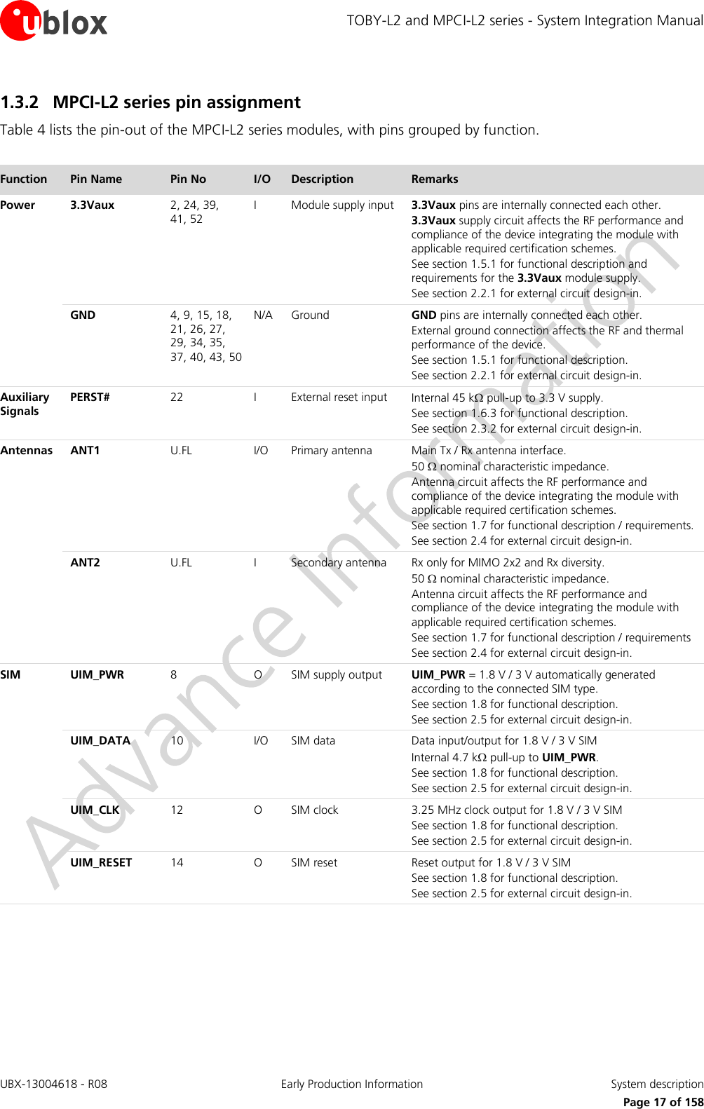
![TOBY-L2 and MPCI-L2 series - System Integration Manual UBX-13004618 - R08 Early Production Information System description Page 19 of 158 1.4 Operating modes TOBY-L2 and MPCI-L2 series modules have several operating modes. The operating modes are defined in Table 5 and described in detail in Table 6, providing general guidelines for operation. General Status Operating Mode Definition Power-down Not-Powered Mode VCC or 3.3Vaux supply not present or below operating range: module is switched off. Power-Off Mode VCC or 3.3Vaux supply within operating range and module is switched off. Normal Operation Idle-Mode Module processor core runs with 32 kHz reference generated by the internal oscillator. Active-Mode Module processor core runs with 26 MHz reference generated by the internal oscillator. Connected-Mode RF Tx/Rx data connection enabled and processor core runs with 26 MHz reference. Table 5: TOBY-L2 and MPCI-L2 series modules operating modes definition Operating Mode Description Transition between operating modes Not-Powered Mode Module is switched off. Application interfaces are not accessible. When VCC or 3.3Vaux supply is removed, the modules enter not-powered mode. When in not-powered mode, TOBY-L2 modules cannot be switched on by PWR_ON, RESET_N or RTC alarm and enter active-mode after applying VCC supply (see 1.6.1). When in not-powered mode, MPCI-L2 modules cannot be switched on by RTC alarm and enter active-mode after applying 3.3Vaux supply (see 1.6.1). Power-Off Mode Module is switched off: normal shutdown by an appropriate power-off event (see 1.6.2). Application interfaces are not accessible. MPCI-L2 modules do not support Power-Off Mode but halt mode (see 1.6.2 and u-blox AT Commands Manual [3], AT+CFUN=127 command). When the modules are switched off by an appropriate power-off event (see 1.6.2), the modules enter power-off mode from active-mode. When in power-off mode, TOBY-L2 modules can be switched on by PWR_ON, RESET_N or an RTC alarm. When in power-off mode, TOBY-L2 modules enter the not-powered mode after removing VCC supply. Idle-Mode Module is switched on with application interfaces disabled or suspended: the module is temporarily not ready to communicate with an external device by means of the application interfaces as configured to reduce the current consumption. The module enters the low power idle-mode whenever possible if power saving is enabled by AT+UPSV (see u-blox AT Commands Manual [3]) reducing current consumption (see 1.5.1.5). With HW flow control enabled and AT+UPSV=1 or AT+UPSV=3, the UART CTS line indicates when the UART is enabled (see 1.9.2.3, 1.9.2.4). With HW flow control disabled, the UART CTS line is fixed to ON state (see 1.9.2.3). Power saving configuration is not enabled by default: it can be enabled by the AT+UPSV command (see the u-blox AT Commands Manual [3]). The modules automatically switch from active-mode to low power idle-mode whenever possible if power saving is enabled (see sections 1.5.1.5, 1.9.1.4, 1.9.2.4 and u-blox AT Commands Manual [3], AT+UPSV). The modules wake up from idle-mode to active-mode in the following events: Automatic periodic monitoring of the paging channel for the paging block reception according to network conditions (see 1.5.1.5) The connected USB host forces a remote wakeup of the module as USB device (see 1.9.1.4) Automatic periodic enable of the UART interface to receive / send data, with AT+UPSV=1 (see 1.9.2.4) Data received on UART interface, with HW flow control disabled and AT+UPSV=1 (see 1.9.2.4) RTS input set ON by the host DTE, with HW flow control disabled and AT+UPSV=2 (see 1.9.2.4) DTR input set ON by the host DTE, with AT+UPSV=3 (see 1.9.2.4) The connected SDIO device forces a wakeup of the module as SDIO host (see 1.9.4) A preset RTC alarm occurs (see u-blox AT Commands Manual [3], AT+CALA)](https://usermanual.wiki/u-blox/TOBYL280.System-Integrators-Manual/User-Guide-2664029-Page-19.png)
![TOBY-L2 and MPCI-L2 series - System Integration Manual UBX-13004618 - R08 Early Production Information System description Page 20 of 158 Operating Mode Description Transition between operating modes Active-Mode Module is switched on with application interfaces enabled or not suspended: the module is ready to communicate with an external device by means of the application interfaces unless power saving configuration is enabled by AT+UPSV (see 1.9.1.4, 1.9.2.4 and u-blox AT Commands Manual [3]). When the modules are switched on by an appropriate power-on event (see 1.6.1), the module enter active-mode from power-off mode. If power saving configuration is enabled by the AT+UPSV command, the module automatically switches from active to idle-mode whenever possible and the module wakes up from idle to active-mode in the events listed above (see idle-mode to active-mode transition description above). When a RF Tx/Rx data connection is initiated or when RF Tx/Rx is required due to a connection previously initiated, the module switches from active to connected-mode. Connected-Mode RF Tx/Rx data connection is in progress. The module is prepared to accept data signals from an external device unless power saving configuration is enabled by AT+UPSV (see sections 1.9.1.4, 1.9.2.4 and u-blox AT Commands Manual [3]). When a data connection is initiated, the module enters connected-mode from idle-mode. If power saving configuration is enabled by the AT+UPSV command, the module automatically switches from connected to active and then idle-mode whenever possible and the module wakes up from idle to active and then connected mode if RF Transmission/Reception is necessary. When a data connection is terminated, the module returns to the active-mode. Table 6: TOBY-L2 and MPCI-L2 series modules operating modes description Figure 3 describes the transition between the different operating modes. TOBY-L2 Switch ON:•Apply VCCMPCI-L2 Switch ON:•Apply 3.3VauxIf power saving is enabled and there is no activity for a defined time intervalAny wake up event described in the module operating modes summary table aboveIncoming/outgoing call or other dedicated device network communicationNo RF Tx/Rx in progress, Call terminated, Communication droppedTOBY-L2 Switch ON:•PWR_ON•RESET_N•RTC alarmNot poweredPower offActiveConnected IdleTOBY-L2 Switch OFF:•AT+CPWROFF•RESET_NMPCI-L2:•AT+CFUN=127 and then remove 3.3VauxTOBY-L2:•Remove VCC Figure 3: TOBY-L2 and MPCI-L2 series modules operating modes transition](https://usermanual.wiki/u-blox/TOBYL280.System-Integrators-Manual/User-Guide-2664029-Page-20.png)
![TOBY-L2 and MPCI-L2 series - System Integration Manual UBX-13004618 - R08 Early Production Information System description Page 21 of 158 1.5 Supply interfaces 1.5.1 Module supply input (VCC or 3.3Vaux) TOBY-L2 modules are supplied via the three VCC pins, and MPCI-L2 modules are supplied via the five 3.3Vaux pins. All supply voltages used inside the modules are generated from the VCC or the 3.3Vaux supply input by integrated voltage regulators, including the V_BCKP RTC supply, the V_INT generic digital interface supply, and the VSIM or UIM_PWR SIM interface supply. The current drawn by the TOBY-L2 and MPCI-L2 series modules through the VCC or 3.3Vaux pins can vary by several orders of magnitude depending on radio access technology, operation mode and state. It is important that the supply source is able to support both the high peak of current consumption during 2G transmission at maximum RF power level (as described in the section 1.5.1.2) and the high average current consumption during 3G and LTE transmission at maximum RF power level (as described in the sections 1.5.1.3 and 1.5.1.4). 1.5.1.1 VCC or 3.3Vaux supply requirements Table 7 summarizes the requirements for the VCC or 3.3Vaux modules supply. See section 2.2.1 for suggestions to properly design a VCC or 3.3Vaux supply circuit compliant with the requirements listed in Table 7. The supply circuit affects the RF compliance of the device integrating TOBY-L2 and MPCI-L2 series modules with applicable required certification schemes as well as antenna circuit design. Compliance is guaranteed if the requirements summarized in the Table 7 are fulfilled. Item Requirement Remark VCC or 3.3Vaux nominal voltage Within VCC or 3.3Vaux normal operating range: See “Supply/Power pins” section in the TOBY-L2 Data Sheet [1] or in the MPCI-L2 Data Sheet [2]. The modules cannot be switched on if the supply voltage is below the normal operating range minimum limit. VCC or 3.3Vaux voltage during normal operation Within VCC or 3.3Vaux extended operating range: See “Supply/Power pins” section in the TOBY-L2 Data Sheet [1] or in the MPCI-L2 Data Sheet [2]. The modules may switch off if the supply voltage drops below the extended operating range minimum limit. VCC or 3.3Vaux average current Support with adequate margin the highest averaged current consumption value in connected-mode conditions specified for VCC in TOBY-L2 Data Sheet [1] or specified for 3.3Vaux in MPCI-L2 Data Sheet [2]. The maximum average current consumption can be greater than the specified value according to the actual antenna mismatching, temperature and supply voltage. Sections 1.5.1.2, 1.5.1.3 and 1.5.1.4 describe current consumption profiles in 2G, 3G and LTE connected-mode. VCC or 3.3Vaux peak current Support with margin the highest peak current consumption value in 2G connected-mode conditions specified for VCC in TOBY-L2 Data Sheet [1] or specified for 3.3Vaux in MPCI-L2 Data Sheet [2]. The specified maximum peak of current consumption occurs during GSM single transmit slot in 850/900 MHz connected-mode, in case of mismatched antenna. Section 1.5.1.2 describes 2G Tx peak/pulse current. VCC or 3.3Vaux voltage drop during 2G Tx slots Lower than 400 mV Supply voltage drop values greater than recommended during 2G TDMA transmission slots directly affect the RF compliance with applicable certification schemes. Figure 5 describes supply voltage drop during 2G Tx slots. VCC or 3.3Vaux voltage ripple during RF transmission Noise in the supply has to be minimized High supply voltage ripple values during LTE/3G/2G RF transmissions in connected-mode directly affect the RF compliance with applicable certification schemes. Figure 5 describes supply voltage ripple during RF Tx. VCC or 3.3Vaux under/over-shoot at start/end of Tx slots Absent or at least minimized Supply voltage under-shoot or over-shoot at the start or the end of 2G TDMA transmission slots directly affect the RF compliance with applicable certification schemes. Figure 5 describes supply voltage under/over-shoot Table 7: Summary of VCC or 3.3Vaux modules supply requirements](https://usermanual.wiki/u-blox/TOBYL280.System-Integrators-Manual/User-Guide-2664029-Page-21.png)
![TOBY-L2 and MPCI-L2 series - System Integration Manual UBX-13004618 - R08 Early Production Information System description Page 22 of 158 1.5.1.2 VCC or 3.3Vaux current consumption in 2G connected-mode When a GSM call is established, the VCC or 3.3Vaux module current consumption is determined by the current consumption profile typical of the GSM transmitting and receiving bursts. The peak of current consumption during a transmission slot is strictly dependent on the RF transmitted power, which is regulated by the network. The transmitted power in the transmit slot is also the more relevant factor for determining the average current consumption. If the module is transmitting in 2G single-slot mode in the 850 or 900 MHz bands, at the maximum RF power level (approximately 2 W or 33 dBm in the allocated transmit slot/burst) the current consumption can reach an high peak (see the “Current consumption” section in the TOBY-L2 Data Sheet [1] or the MPCI-L2 Data Sheet [2]) for 576.9 µs (width of the transmit slot/burst) with a periodicity of 4.615 ms (width of 1 frame = 8 slots/burst), so with a 1/8 duty cycle according to GSM TDMA (Time Division Multiple Access). If the module is transmitting in 2G single-slot mode in the 1800 or 1900 MHz bands, the current consumption figures are quite less high than the one in the low bands, due to 3GPP transmitter output power specifications. During a GSM call, current consumption is not so significantly high in receiving or in monitor bursts and is low in the inactive unused bursts. Figure 4 shows an example of the module current consumption profile versus time in 2G single-slot mode. Time [ms]RX slotunused slotunused slotTX slotunused slotunused slotMON slotunused slotRX slotunused slotunused slotTX slotunused slotunused slotMON slotunused slotGSM frame 4.615 ms (1 frame = 8 slots)Current [A]200 mA60-120 mA1900 mAPeak current depends on TX power and actual antenna loadGSM frame 4.615 ms (1 frame = 8 slots)60-120 mA10-40 mA0.01.51.00.52.02.5 Figure 4: VCC or 3.3Vaux current consumption profile versus time during a 2G single-slot call (1 TX slot, 1 RX slot) Figure 5 illustrates VCC or 3.3Vaux voltage profile versus time during a 2G single-slot call, according to the relative VCC or 3.3Vaux current consumption profile described in Figure 4. Time [ms]undershootovershootrippledropVoltage [mV]3.8 V (typ)RX slotunused slotunused slotTX slotunused slotunused slotMON slotunused slotRX slotunused slotunused slotTX slotunused slotunused slotMON slotunused slotGSM frame 4.615 ms (1 frame = 8 slots)GSM frame 4.615 ms (1 frame = 8 slots) Figure 5: VCC or 3.3Vaux voltage profile versus time during a 2G single-slot call (1 TX slot, 1 RX slot)](https://usermanual.wiki/u-blox/TOBYL280.System-Integrators-Manual/User-Guide-2664029-Page-22.png)
![TOBY-L2 and MPCI-L2 series - System Integration Manual UBX-13004618 - R08 Early Production Information System description Page 23 of 158 When a GPRS connection is established, more than one slot can be used to transmit and/or more than one slot can be used to receive. The transmitted power depends on network conditions, which set the peak current consumption, but following the 3GPP specifications the maximum Tx RF power is reduced if more than one slot is used to transmit, so the maximum peak of current is not as high as can be in case of a 2G single-slot call. If the module transmits in GPRS class 12 in the 850 or 900 MHz bands, at the maximum RF power control level, the current consumption can reach a quite high peak but lower than the one achievable in 2G single-slot mode. This happens for 2.307 ms (width of the 4 transmit slots/bursts) with a periodicity of 4.615 ms (width of 1 frame = 8 slots/bursts), so with a 1/2 duty cycle, according to 2G TDMA. If the module is in GPRS connected mode in the 1800 or 1900 MHz bands, the current consumption figures are quite less high than the one in the low bands, due to 3GPP transmitter output power specifications. Figure 6 reports the current consumption profiles in GPRS class 12 connected mode, in the 850 or 900 MHz bands, with 4 slots used to transmit and 1 slot used to receive. Time [ms]RX slotunused slotTX slotTX slotTX slotTX slotMON slotunused slotRX slotunused slotTX slotTX slotTX slotTX slotMON slotunused slotGSM frame 4.615 ms (1 frame = 8 slots)Current [A]200mA60-130mAPeak current depends on TX power and actual antenna loadGSM frame 4.615 ms (1 frame = 8 slots)1600 mA0.01.51.00.52.02.5 Figure 6: VCC or 3.3Vaux current consumption profile during a 2G GPRS/EDGE multi-slot connection (4 TX slots, 1 RX slot) In case of EDGE connections the VCC current consumption profile is very similar to the GPRS current profile, so the image shown in Figure 6, representing the current consumption profile in GPRS class 12 connected mode, is valid for the EDGE class 12 connected mode as well.](https://usermanual.wiki/u-blox/TOBYL280.System-Integrators-Manual/User-Guide-2664029-Page-23.png)
![TOBY-L2 and MPCI-L2 series - System Integration Manual UBX-13004618 - R08 Early Production Information System description Page 24 of 158 1.5.1.3 VCC or 3.3Vaux current consumption in 3G connected mode During a 3G connection, the module can transmit and receive continuously due to the Frequency Division Duplex (FDD) mode of operation with the Wideband Code Division Multiple Access (WCDMA). The current consumption depends again on output RF power, which is always regulated by network commands. These power control commands are logically divided into a slot of 666 µs, thus the rate of power change can reach a maximum rate of 1.5 kHz. There are no high current peaks as in the 2G connection, since transmission and reception are continuously enabled due to FDD WCDMA implemented in the 3G that differs from the TDMA implemented in the 2G case. In the worst scenario, corresponding to a continuous transmission and reception at maximum output power (approximately 250 mW or 24 dBm), the average current drawn by the module at the VCC pins is high (see the “Current consumption” section in TOBY-L2 Data Sheet [1] or in MPCI-L2 Data Sheet [2]). Even at lowest output RF power (approximately 0.01 µW or -50 dBm), the current is still not so low due to module baseband processing and transceiver activity. Figure 7 shows an example of current consumption profile of the module in 3G WCDMA/DC-HSPA+ continuous transmission mode. Time [ms]3G frame 10 ms (1 frame = 15 slots)Current [mA]Current consumption value depends on TX power and actual antenna load170 mA1 slot 666 µs850 mA0300200100500400600700 Figure 7: VCC or 3.3Vaux current consumption profile versus time during a 3G connection (TX and RX continuously enabled)](https://usermanual.wiki/u-blox/TOBYL280.System-Integrators-Manual/User-Guide-2664029-Page-24.png)
![TOBY-L2 and MPCI-L2 series - System Integration Manual UBX-13004618 - R08 Early Production Information System description Page 25 of 158 1.5.1.4 VCC or 3.3Vaux current consumption in LTE connected-mode During a LTE connection, the module can transmit and receive continuously due to LTE radio access technology. The current consumption is strictly dependent on the transmitted RF output power, which is always regulated by network commands. These power control commands are logically divided into a slot of 0.5 ms (time length of one Resource Block), thus the rate of power change can reach a maximum rate of 2 kHz. Figure 8 shows an example of the module current consumption profile versus time in LTE connected-mode. Detailed current consumption values can be found in TOBY-L2 Data Sheet [1] and in MPCI-L2 Data Sheet [2]. Time [ms]Current [mA]Current consumption value depends on TX power and actual antenna load1 Slot1 Resource Block (0.5 ms) 1 LTE Radio Frame (10 ms)0300200100500400600700 Figure 8: VCC or 3.3Vaux current consumption profile versus time during LTE connection (TX and RX continuously enabled)](https://usermanual.wiki/u-blox/TOBYL280.System-Integrators-Manual/User-Guide-2664029-Page-25.png)
![TOBY-L2 and MPCI-L2 series - System Integration Manual UBX-13004618 - R08 Early Production Information System description Page 26 of 158 1.5.1.5 VCC or 3.3Vaux current consumption in cyclic idle/active mode (power saving enabled) The power saving configuration is by default disabled, but it can be enabled using the AT+UPSV command (see the u-blox AT Commands Manual [3]). When power saving is enabled, the module automatically enters the low power idle-mode whenever possible, reducing current consumption. During low power idle-mode, the module processor runs with 32 kHz reference clock frequency. When the power saving configuration is enabled and the module is registered or attached to a network, the module automatically enters the low power idle-mode whenever possible, but it must periodically monitor the paging channel of the current base station (paging block reception), in accordance to the 2G/3G/LTE system requirements, even if connected-mode is not enabled by the application. When the module monitors the paging channel, it wakes up to the active-mode, to enable the reception of paging block. In between, the module switches to low power idle-mode. This is known as discontinuous reception (DRX). The module processor core is activated during the paging block reception, and automatically switches its reference clock frequency from 32 kHz to the 26 MHz used in active-mode. The time period between two paging block receptions is defined by the network. This is the paging period parameter, fixed by the base station through broadcast channel sent to all users on the same serving cell: In case of 2G radio access technology, the paging period can vary from 470.8 ms (DRX = 2, length of 2 x 51 2G frames = 2 x 51 x 4.615 ms) up to 2118.4 ms (DRX = 9, length of 9 x 51 2G frames = 9 x 51 x 4.615 ms) In case of 3G radio access technology, the paging period can vary from 640 ms (DRX = 6, i.e. length of 26 3G frames = 64 x 10 ms) up to 5120 ms (DRX = 9, length of 29 3G frames = 512 x 10 ms). In case of LTE radio access technology, the paging period can vary from 320 ms (DRX = 5, i.e. length of 25 LTE frames = 32 x 10 ms) up to 2560 ms (DRX = 8, length of 28 LTE frames = 256 x 10 ms). Figure 9 illustrates a typical example of the module current consumption profile when power saving is enabled. The module is registered with network, automatically enters the low power idle-mode and periodically wakes up to active-mode to monitor the paging channel for the paging block reception. Detailed current consumption values can be found in TOBY-L2 Data Sheet [1] and in MPCI-L2 Data Sheet [2]. ~50 msIDLE MODE ACTIVE MODE IDLE MODEActive Mode EnabledIdle Mode Enabled2G case: 0.44-2.09 s 3G case: 0.61-5.09 s LTE case: 0.27-2.51 sIDLE MODE~50 msACTIVE MODETime [s]Current [mA]Time [ms]Current [mA]RX Enabled01000100 Figure 9: VCC or 3.3Vaux current consumption profile with power saving enabled and module registered with the network: the module is in idle-mode and periodically wakes up to active-mode to monitor the paging channel for paging block reception](https://usermanual.wiki/u-blox/TOBYL280.System-Integrators-Manual/User-Guide-2664029-Page-26.png)
![TOBY-L2 and MPCI-L2 series - System Integration Manual UBX-13004618 - R08 Early Production Information System description Page 27 of 158 1.5.1.6 VCC or 3.3Vaux current consumption in fixed active-mode (power saving disabled) When power saving is disabled, the module does not automatically enter the low power idle-mode whenever possible: the module remains in active-mode. Power saving configuration is by default disabled. It can also be disabled using the AT+UPSV command (see u-blox AT Commands Manual [3] for detail usage). The module processor core is activated during idle-mode, and the 26 MHz reference clock frequency is used. It would draw more current during the paging period than that in the power saving mode. Figure 10 illustrates a typical example of the module current consumption profile when power saving is disabled. In such case, the module is registered with the network and while active-mode is maintained, the receiver is periodically activated to monitor the paging channel for paging block reception. Detailed current consumption values can be found in TOBY-L2 Data Sheet [1] and in MPCI-L2 Data Sheet [2]. ACTIVE MODE2G case: 0.44-2.09 s 3G case: 0.61-5.09 sLTE case: 0.32-2.56 sPaging periodTime [s]Current [mA]Time [ms]Current [mA]RX Enabled01000100 Figure 10: VCC or 3.3Vaux current consumption profile with power saving disabled and module registered with the network: active-mode is always held and the receiver is periodically activated to monitor the paging channel for paging block reception](https://usermanual.wiki/u-blox/TOBYL280.System-Integrators-Manual/User-Guide-2664029-Page-27.png)
![TOBY-L2 and MPCI-L2 series - System Integration Manual UBX-13004618 - R08 Early Production Information System description Page 28 of 158 1.5.2 RTC supply input/output (V_BCKP) The RTC supply V_BCKP pin is not available on MPCI-L2 series modules. The V_BCKP pin of TOBY-L2 series modules connects the supply for the Real Time Clock (RTC). A linear LDO regulator integrated in the Power Management Unit internally generates this supply, as shown in Figure 11, with low current capability (see the TOBY-L2 series Data Sheet [1]). The output of this regulator is always enabled when the main module voltage supply applied to the VCC pins is within the valid operating range. Baseband Processor70VCC71VCC72VCC3V_BCKPLinear LDOPower ManagementTOBY-L2 series32 kHzRTC Figure 11: TOBY-L2 series RTC supply (V_BCKP) simplified block diagram The RTC provides the module time reference (date and time) that is used to set the wake-up interval during the low power idle-mode periods, and is able to make available the programmable alarm functions. The RTC functions are available also in power-down mode when the V_BCKP voltage is within its valid range (specified in the “Input characteristics of Supply/Power pins” table in TOBY-L2 series Data Sheet [1]). The RTC can be supplied from an external back-up battery through the V_BCKP, when the main module voltage supply is not applied to the VCC pins. This lets the time reference (date and time) run until the V_BCKP voltage is within its valid range, even when the main supply is not provided to the module. Consider that the module cannot switch on if a valid voltage is not present on VCC even when the RTC is supplied through V_BCKP (meaning that VCC is mandatory to switch on the module). The RTC has very low current consumption, but is highly temperature dependent. For example, V_BCKP current consumption at the maximum operating temperature can be higher than the typical value at 25 °C specified in the “Input characteristics of Supply/Power pins” table in the TOBY-L2 series Data Sheet [1]. If V_BCKP is left unconnected and the module main supply is not applied to the VCC pins, the RTC is supplied from the bypass capacitor mounted inside the module. However, this capacitor is not able to provide a long buffering time: within few milliseconds the voltage on V_BCKP will go below the valid range (1.4 V min). This has no impact on cellular connectivity, as all the module functionalities do not rely on date and time setting.](https://usermanual.wiki/u-blox/TOBYL280.System-Integrators-Manual/User-Guide-2664029-Page-28.png)
![TOBY-L2 and MPCI-L2 series - System Integration Manual UBX-13004618 - R08 Early Production Information System description Page 29 of 158 1.5.3 Generic digital interfaces supply output (V_INT) The generic digital interfaces supply V_INT pin is not available on MPCI-L2 series modules. The V_INT output pin of the TOBY-L2 series modules is connected to an internal 1.8 V supply with current capability specified in the TOBY-L2 series Data Sheet [1]. This supply is internally generated by a switching step-down regulator integrated in the Power Management Unit and it is internally used to source the generic digital I/O interfaces of the TOBY-L2 module, as described in Figure 12. The output of this regulator is enabled when the module is switched on and it is disabled when the module is switched off. Baseband Processor70VCC71VCC72VCC5V_INTSwitchingStep-DownPower ManagementTOBY-L2 seriesDigital I/O Figure 12: TOBY-L2 series generic digital interfaces supply output (V_INT) simplified block diagram The switching regulator operates in Pulse Width Modulation (PWM) mode for greater efficiency at high output loads and it automatically switches to Pulse Frequency Modulation (PFM) power save mode for greater efficiency at low output loads. The V_INT output voltage ripple is specified in the TOBY-L2 series Data Sheet [1].](https://usermanual.wiki/u-blox/TOBYL280.System-Integrators-Manual/User-Guide-2664029-Page-29.png)
![TOBY-L2 and MPCI-L2 series - System Integration Manual UBX-13004618 - R08 Early Production Information System description Page 30 of 158 1.6 System function interfaces 1.6.1 Module power-on The PWR_ON input pin is not available on MPCI-L2 series modules. When the TOBY-L2 and MPCI-L2 series modules are in the not-powered mode (switched off, i.e. the VCC or 3.3Vaux module supply is not applied), they can be switched on as following: Rising edge on the VCC or 3.3Vaux supply input to a valid voltage for module supply, so that the module switches on applying a proper VCC or 3.3Vaux supply within the normal operating range. Alternately, the RESET_N or PERST# pin can be held to the low level during the VCC or 3.3Vaux rising edge, so that the module switches on releasing the RESET_N or PERST# pin when the VCC or 3.3Vaux module supply voltage stabilizes at its proper nominal value within the normal operating range. The status of the PWR_ON input pin of TOBY-L2 modules while applying the VCC module supply is not relevant: during this phase the PWR_ON pin can be set high or low by the external circuit. When the TOBY-L2 modules are in the power-off mode (i.e. switched off with valid VCC module supply applied), they can be switched on as following: Low level on the PWR_ON pin, which is normally set high by an internal pull-up, for a valid time period. Low level on the RESET_N pin, which is normally set high by an internal pull-up, for a valid time period. RTC alarm, i.e. pre-programmed alarm by AT+CALA command (see u-blox AT Commands Manual [3]). As described in Figure 13, the TOBY-L2 series PWR_ON input is equipped with an internal active pull-up resistor to the VCC module supply: the PWR_ON input voltage thresholds are different from the other generic digital interfaces. Detailed electrical characteristics are described in TOBY-L2 series Data Sheet [1]. Baseband Processor20PWR_ONTOBY-L2 seriesVCCPower-onPower ManagementPower-on50k Figure 13: TOBY-L2 series PWR_ON input description](https://usermanual.wiki/u-blox/TOBYL280.System-Integrators-Manual/User-Guide-2664029-Page-30.png)
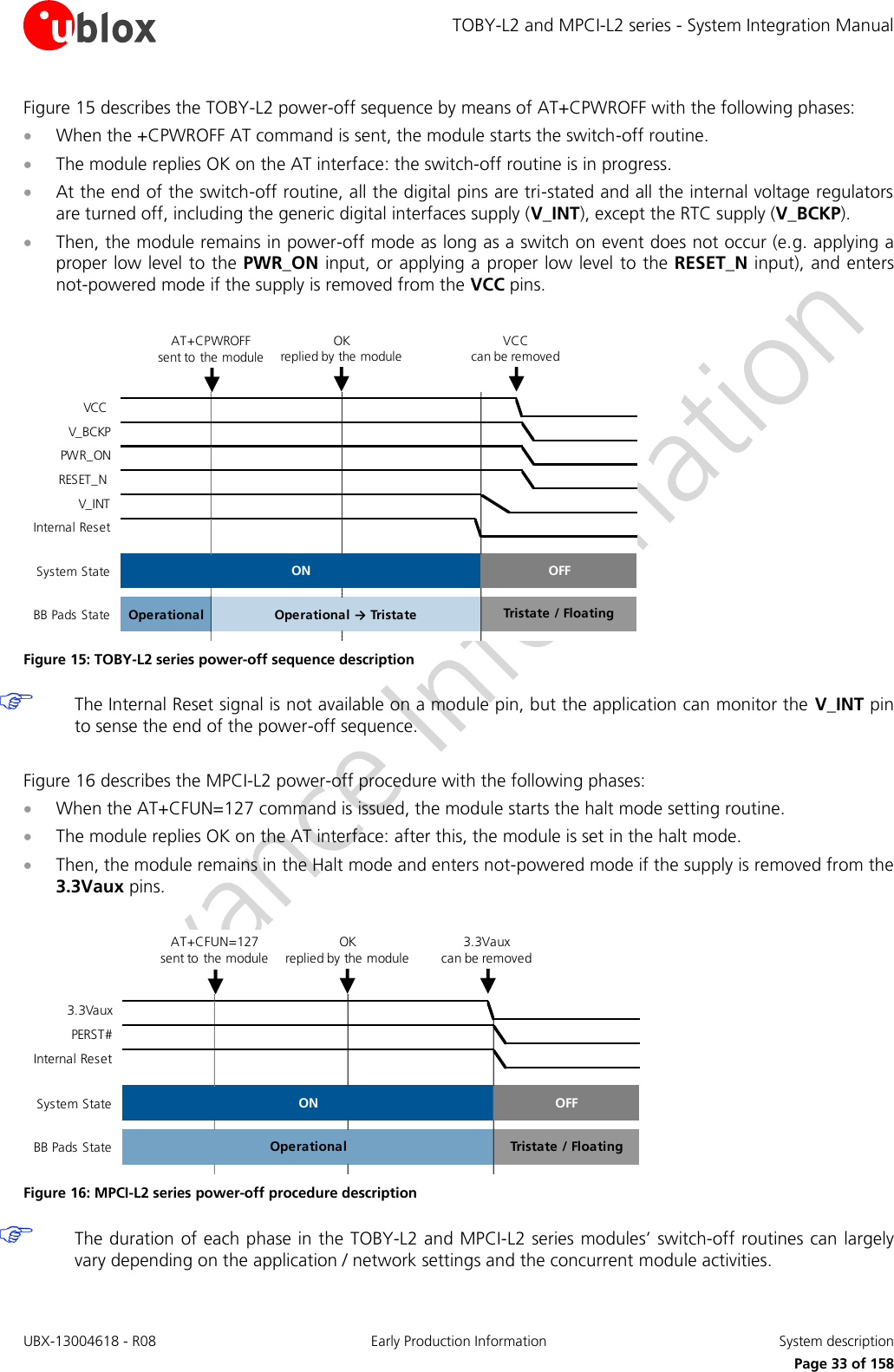
![TOBY-L2 and MPCI-L2 series - System Integration Manual UBX-13004618 - R08 Early Production Information System description Page 31 of 158 Figure 14 shows the module power-on sequence from the not-powered mode, describing the following phases: The external supply is applied to the VCC or 3.3Vaux module supply inputs, representing the start-up event. The PWR_ON and the RESET_N or PERST# pins suddenly rise to high logic level due to internal pull-ups. The V_BCKP RTC supply output is suddenly enabled by the module as VCC reaches a valid voltage value. All the generic digital pins of the module are tri-stated until the switch-on of their supply source (V_INT). The internal reset signal is held low: the baseband core and all the digital pins are held in the reset state. The reset state of all the digital pins is reported in the pin description table of TOBY-L2 Series Data Sheet [1]. When the internal reset signal is released, any digital pin is set in a proper sequence from the reset state to the default operational configured state. The duration of this pins’ configuration phase differs within generic digital interfaces and the USB interface due to host / device enumeration timings (see section 1.9.1). The module is fully ready to operate after all interfaces are configured. VCC or 3.3VauxV_BCKPPWR_ONRESET_N or PERST#V_INTInternal ResetSystem StateBB Pads StateInternal Reset → Operational OperationalTristate / Floating Internal ResetOFFON0 ms~10 ms~20 sStart of interface configurationModule interfaces are configuredStart-up event~5 ms Figure 14: TOBY-L2 and MPCI-L2 series power-on sequence description The Internal Reset signal is not available on a module pin, but the host application can monitor: The V_INT pin to sense the start of the TOBY-L2 module power-on sequence. The USB interface to sense the start of the MPCI-L2 module power-on sequence: the module, as USB device, informs the host of the attach event via a reply on its status change pipe for proper bus enumeration process according to Universal Serial Bus Revision 2.0 specification [6]. Before the switch-on of the generic digital interface supply source (V_INT) of the module, no voltage driven by an external application should be applied to any generic digital interface of TOBY-L2 module. Before the TOBY-L2 and MPCI-L2 series module is fully ready to operate, the host application processor should not send any AT command over the AT communication interfaces (USB, UART) of the module.](https://usermanual.wiki/u-blox/TOBYL280.System-Integrators-Manual/User-Guide-2664029-Page-31.png)
![TOBY-L2 and MPCI-L2 series - System Integration Manual UBX-13004618 - R08 Early Production Information System description Page 32 of 158 1.6.2 Module power-off TOBY-L2 series can be properly switched off by: AT+CPWROFF command (see u-blox AT Commands Manual [3]). The current parameter settings are saved in the module’s non-volatile memory and a proper network detach is performed. The MPCI-L2 series modules do not switch off by the AT+CPWROFF command as the TOBY-L2 modules, but the AT+CPWROFF command causes a reset (reboot) of the module due to the MPCI-L2 module’s internal configuration: the command stores the actual parameter settings in the non-volatile memory of MPCI-L2 modules and performs a network detach, with a subsequent reset (reboot) of the module. An abrupt under-voltage shutdown occurs on TOBY-L2 and MPCI-L2 series modules when the VCC or 3.3Vaux module supply is removed. If this occurs, it is not possible to perform the storing of the current parameter settings in the module’s non-volatile memory or to perform the proper network detach. It is highly recommended to avoid an abrupt removal of the VCC supply during TOBY-L2 modules normal operations: the power off procedure must be started by the AT+CPWROFF command, waiting the command response for a proper time period (see u-blox AT Commands Manual [3]), and then a proper VCC supply has to be held at least until the end of the modules’ internal power off sequence, which occurs when the generic digital interfaces supply output (V_INT) is switched off by the module. It is highly recommended to avoid an abrupt removal of the 3.3Vaux supply during MPCI-L2 modules normal operations: the power off procedure must be started by setting the MPCI-L2 module in the halt mode by the AT+CFUN=127 command (which stores the actual parameter settings in the non-volatile memory of the module and performs a network detach), waiting the command response for a proper time period (see the u-blox AT Commands Manual [3]), and then the 3.3Vaux supply can be removed. An abrupt hardware shutdown occurs on TOBY-L2 series modules when a low level is applied on the RESET_N pin for a specific time period. In this case, the current parameter settings are not saved in the module’s non-volatile memory and a proper network detach is not performed. It is highly recommended to avoid an abrupt hardware shutdown of the module by forcing a low level on the RESET_N input pin during module normal operation: the RESET_N line should be set low only if reset or shutdown via AT commands fails or if the module does not reply to a specific AT command after a time period longer than the one defined in the u-blox AT Commands Manual [3]. An over-temperature or an under-temperature shutdown occurs on TOBY-L2 and MPCI-L2 series modules when the temperature measured within the cellular module reaches the dangerous area, if the optional Smart Temperature Supervisor feature is enabled and configured by the dedicated AT command. For more details see u-blox AT Commands Manual [3], +USTS AT command. The Smart Temperature Supervisor feature is not supported by the “00”, “01”, and “50” product versions.](https://usermanual.wiki/u-blox/TOBYL280.System-Integrators-Manual/User-Guide-2664029-Page-32.png)
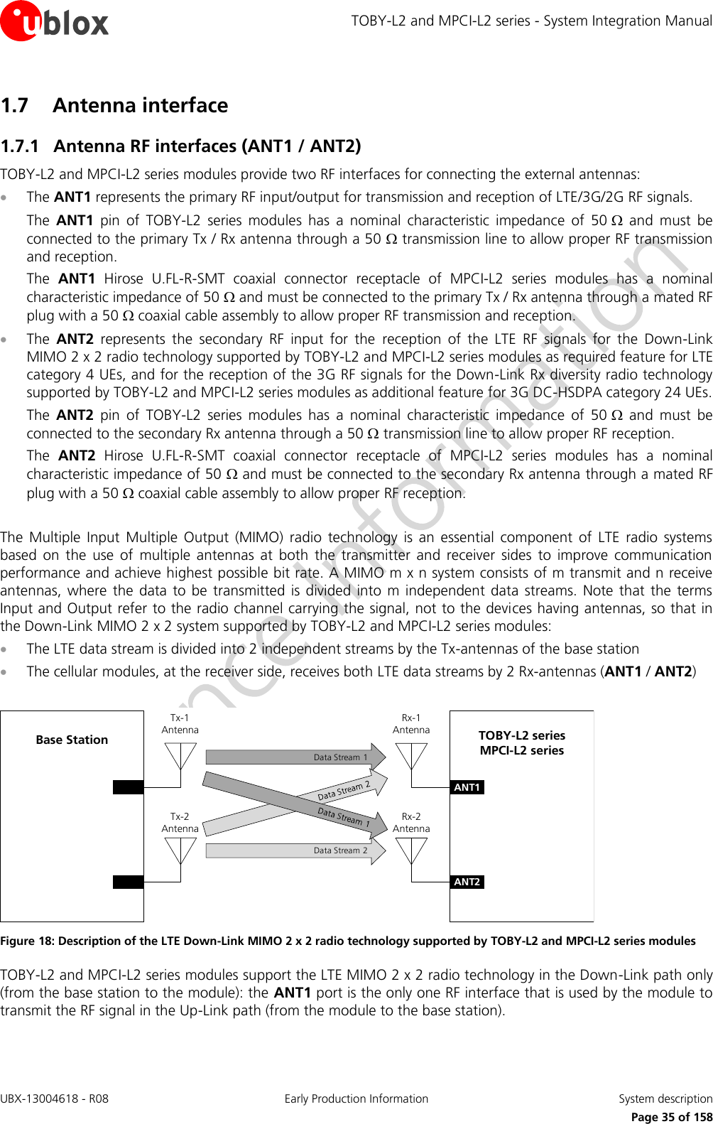
![TOBY-L2 and MPCI-L2 series - System Integration Manual UBX-13004618 - R08 Early Production Information System description Page 34 of 158 1.6.3 Module reset TOBY-L2 and MPCI-L2 series modules can be properly reset (rebooted) by: AT+CFUN command (see u-blox AT Commands Manual [3]). MPCI-L2 series modules can be additionally properly reset (rebooted) by: AT+CPWROFF command (see u-blox AT Commands Manual [3]): the behavior differs than TOBY-L2 series, as MPCI-L2 modules will reboot rather than remain switched off due to modules’ internal configuration. In the cases listed above an “internal” or “software” reset of the module is executed: the current parameter settings are saved in the module’s non-volatile memory and a proper network detach is performed. An abrupt hardware reset occurs on TOBY-L2 and MPCI-L2 series modules when a low level is applied on the RESET_N or PERST# input pin for a specific time period. In this case, the current parameter settings are not saved in the module’s non-volatile memory and a proper network detach is not performed. It is highly recommended to avoid an abrupt hardware reset of the module by forcing a low level on the RESET_N or PERST# input during modules normal operation: the RESET_N or PERST# line should be set low only if reset or shutdown via AT commands fails or if the module does not provide a reply to a specific AT command after a time period longer than the one defined in the u-blox AT Commands Manual [3]. As described in Figure 17, the RESET_N and PERST# input pins are equipped with an internal pull-up to the VCC supply in the TOBY-L2 series and to the 3.3 V in the MPCI-L2 series. Baseband Processor23RESET_NTOBY-L2 seriesVCCResetPower ManagementReset50kBaseband Processor22PERST#MPCI-L2 seriesResetPower ManagementReset45k3.3 V Figure 17: TOBY-L2 and MPCI-L2 series RESET_N and PERST# input equivalent circuit description For more electrical characteristics details see TOBY-L2 Data Sheet [1] and MPCI-L2 Data Sheet [2]. 1.6.4 Module configuration selection by host processor The HOST_SELECT0 and HOST_SELECT1 pins are not available on MPCI-L2 series modules. The selection of the module configuration by the host application processor over the HOST_SELECT0 and HOST_SELECT1 pins is not supported by TOBY-L2 “00”, “01”, and “50” product versions. TOBY-L2 series modules include two input pins (HOST_SELECT0 and HOST_SELECT1) for the selection of the module configuration by the host application processor.](https://usermanual.wiki/u-blox/TOBYL280.System-Integrators-Manual/User-Guide-2664029-Page-34.png)
![TOBY-L2 and MPCI-L2 series - System Integration Manual UBX-13004618 - R08 Early Production Information System description Page 36 of 158 1.7.1.1 Antenna RF interfaces requirements Table 8, Table 9 and Table 10 summarize the requirements for the antennas RF interfaces (ANT1 / ANT2). See section 2.4.1 for suggestions to properly design antennas circuits compliant with these requirements. The antenna circuits affect the RF compliance of the device integrating TOBY-L2 and MPCI-L2 series modules with applicable required certification schemes (for more details see section 4). Compliance is guaranteed if the antenna RF interfaces (ANT1 / ANT2) requirements summarized in Table 8, Table 9 and Table 10 are fulfilled. Item Requirements Remarks Impedance 50 nominal characteristic impedance The impedance of the antenna RF connection must match the 50 impedance of the ANT1 port. Frequency Range See the TOBY-L2 series Data Sheet [1] and the MPCI-L2 series Data Sheet [2] The required frequency range of the antenna connected to ANT1 port depends on the operating bands of the used cellular module and the used mobile network. Return Loss S11 < -10 dB (VSWR < 2:1) recommended S11 < -6 dB (VSWR < 3:1) acceptable The Return loss or the S11, as the VSWR, refers to the amount of reflected power, measuring how well the primary antenna RF connection matches the 50 characteristic impedance of the ANT1 port. The impedance of the antenna termination must match as much as possible the 50 nominal impedance of the ANT1 port over the operating frequency range, reducing as much as possible the amount of reflected power. Efficiency > -1.5 dB ( > 70% ) recommended > -3.0 dB ( > 50% ) acceptable The radiation efficiency is the ratio of the radiated power to the power delivered to antenna input: the efficiency is a measure of how well an antenna receives or transmits. The radiation efficiency of the antenna connected to the ANT1 port needs to be enough high over the operating frequency range to comply with the Over-The-Air (OTA) radiated performance requirements, as Total Radiated Power (TRP) and the Total Isotropic Sensitivity (TIS), specified by applicable related certification schemes. Maximum Gain According to radiation exposure limits The power gain of an antenna is the radiation efficiency multiplied by the directivity: the gain describes how much power is transmitted in the direction of peak radiation to that of an isotropic source. The maximum gain of the antenna connected to ANT1 port must not exceed the herein stated value to comply with regulatory agencies radiation exposure limits. For additional info see the section 4.2.2. Input Power > 33 dBm ( > 2 W ) The antenna connected to the ANT1 port must support with adequate margin the maximum power transmitted by the modules. Table 8: Summary of primary Tx/Rx antenna RF interface (ANT1) requirements](https://usermanual.wiki/u-blox/TOBYL280.System-Integrators-Manual/User-Guide-2664029-Page-36.png)
![TOBY-L2 and MPCI-L2 series - System Integration Manual UBX-13004618 - R08 Early Production Information System description Page 37 of 158 Item Requirements Remarks Impedance 50 nominal characteristic impedance The impedance of the antenna RF connection must match the 50 impedance of the ANT2 port. Frequency Range See the TOBY-L2 series Data Sheet [1] and the MPCI-L2 series Data Sheet [2] The required frequency range of the antennas connected to ANT2 port depends on the operating bands of the used cellular module and the used Mobile Network. Return Loss S11 < -10 dB (VSWR < 2:1) recommended S11 < -6 dB (VSWR < 3:1) acceptable The Return loss or the S11, as the VSWR, refers to the amount of reflected power, measuring how well the secondary antenna RF connection matches the 50 characteristic impedance of the ANT2 port. The impedance of the antenna termination must match as much as possible the 50 nominal impedance of the ANT2 port over the operating frequency range, reducing as much as possible the amount of reflected power. Efficiency > -1.5 dB ( > 70% ) recommended > -3.0 dB ( > 50% ) acceptable The radiation efficiency is the ratio of the radiated power to the power delivered to antenna input: the efficiency is a measure of how well an antenna receives or transmits. The radiation efficiency of the antenna connected to the ANT2 port needs to be enough high over the operating frequency range to comply with the Over-The-Air (OTA) radiated performance requirements, as the TIS, specified by applicable related certification schemes. Table 9: Summary of secondary Rx antenna RF interface (ANT2) requirements Item Requirements Remarks Efficiency imbalance < 0.5 dB recommended < 1.0 dB acceptable The radiation efficiency imbalance is the ratio of the primary (ANT1) antenna efficiency to the secondary (ANT2) antenna efficiency: the efficiency imbalance is a measure of how much better an antenna receives or transmits compared to the other antenna. The radiation efficiency of the secondary antenna needs to be roughly the same of the radiation efficiency of the primary antenna for good RF performance. Envelope Correlation Coefficient < 0.4 recommended < 0.5 acceptable The Envelope Correlation Coefficient (ECC) between the primary (ANT1) and the secondary (ANT2) antenna is an indicator of 3D radiation pattern similarity between the two antennas: low ECC results from antenna patterns with radiation lobes in different directions. The ECC between primary and secondary antenna needs to be enough low to comply with radiated performance requirements specified by related certification schemes. Isolation > 15 dB recommended > 10 dB acceptable The antenna to antenna isolation is the loss between the primary (ANT1) and the secondary (ANT2) antenna: high isolation results from low coupled antennas. The isolation between primary and secondary antenna needs to be high for good RF performance. Table 10: Summary of primary (ANT1) and secondary (ANT2) antennas relationship requirements](https://usermanual.wiki/u-blox/TOBYL280.System-Integrators-Manual/User-Guide-2664029-Page-37.png)
![TOBY-L2 and MPCI-L2 series - System Integration Manual UBX-13004618 - R08 Early Production Information System description Page 38 of 158 1.7.2 Antenna detection interface (ANT_DET) Antenna detection (ANT_DET) is not available on MPCI-L2 series modules. Antenna detection (ANT_DET) is not supported by TOBY-L2 “00”, “01”, and “50” product versions. The antenna detection is based on ADC measurement. The ANT_DET pin is an Analog to Digital Converter (ADC) provided to sense the antenna presence. The antenna detection function provided by ANT_DET pin is an optional feature that can be implemented if the application requires it. The antenna detection is forced by the +UANTR AT command. See the u-blox AT Commands Manual [3] for more details on this feature. The ANT_DET pin generates a DC current (for detailed characteristics see the TOBY-L2 series Data Sheet [1]) and measures the resulting DC voltage, thus determining the resistance from the antenna connector provided on the application board to GND. So, the requirements to achieve antenna detection functionality are the following: an RF antenna assembly with a built-in resistor (diagnostic circuit) must be used an antenna detection circuit must be implemented on the application board See section 2.4.2 for antenna detection circuit on application board and diagnostic circuit on antenna assembly design-in guidelines. 1.8 SIM interface 1.8.1 SIM interface TOBY-L2 and MPCI-L2 series modules provide high-speed SIM/ME interface including automatic detection and configuration of the voltage required by the connected SIM card or chip. Both 1.8 V and 3 V SIM types are supported. Activation and deactivation with automatic voltage switch from 1.8 V to 3 V are implemented, according to ISO-IEC 7816-3 specifications. The VSIM or UIM_PWR supply output provides internal short circuit protection to limit start-up current and protect the SIM to short circuits. The SIM driver supports the PPS (Protocol and Parameter Selection) procedure for baud-rate selection, according to the values determined by the SIM card or chip. 1.8.2 SIM detection interface SIM detection (GPIO5) is not available on MPCI-L2 series modules. SIM detection (GPIO5) is not supported by TOBY-L2 “00”, “01”, and “50” product versions. The GPIO5 pin is by default configured to detect the SIM card mechanical / physical presence. The pin is configured as input with an internal active pull-down enabled, and it can sense SIM card presence only if properly connected to the mechanical switch of a SIM card holder as described in section 2.5: Low logic level at GPIO5 input pin is recognized as SIM card not present High logic level at GPIO5 input pin is recognized as SIM card present The SIM card detection function provided by GPIO5 pin is an optional feature that can be implemented / used or not according to the application requirements: an Unsolicited Result Code (URC) is generated each time that there is a change of status (for more details see the u-blox AT Commands Manual [3]). The optional function “SIM card hot insertion/removal” can be additionally enabled on the GPIO5 pin by specific AT command (see the u-blox AT Commands Manual [3]).](https://usermanual.wiki/u-blox/TOBYL280.System-Integrators-Manual/User-Guide-2664029-Page-38.png)
![TOBY-L2 and MPCI-L2 series - System Integration Manual UBX-13004618 - R08 Early Production Information System description Page 39 of 158 1.9 Data communication interfaces TOBY-L2 and MPCI-L2 series modules provide the following serial communication interface: USB interface: High-Speed USB 2.0 compliant interface available for the communication with an external host application processor, for AT commands, data communication, FW upgrade by means of the FOAT feature, FW upgrade by means of the u-blox EasyFlash tool and for diagnostic purpose (see section 1.9.1 for functional description) TOBY-L2 series modules additionally provide the following serial communication interfaces: UART interface: asynchronous serial interface available for the communication with an external host application processor, for AT commands, data communication, FW upgrade by means of the FOAT feature (see section 1.9.2 for functional description) DDC interface: I2C bus compatible interface available for the communication with u-blox GNSS positioning chips/modules and with external I2C devices as an audio codec (see section 1.9.3 for functional description) SDIO interface: Secure Digital Input Output interface available for the communication with an external Wi-Fi chip or module (see section 1.9.4 for functional description) 1.9.1 Universal Serial Bus (USB) 1.9.1.1 USB features TOBY-L2 and MPCI-L2 series modules include a High-Speed USB 2.0 compliant interface with maximum data rate of 480 Mb/s, representing the main interface for transferring high speed data with a host application processor: the USB interface is available for AT commands, data communication, FW upgrade by means of the FOAT feature, FW upgrade by means of the u-blox EasyFlash tool and for diagnostic purpose. The module itself acts as a USB device and can be connected to a USB host such as a Personal Computer or an embedded application microprocessor equipped with compatible drivers. The USB_D+ / USB_D- lines carry the USB serial bus data and signaling, providing all the functionalities for the bus attachment, configuration, enumeration, suspension or remote wakeup according to the Universal Serial Bus Revision 2.0 specification [6] The additional VUSB_DET input is available as an optional feature to sense the host VBUS voltage (5.0 V typical). The VUSB_DET functionality is not supported by TOBY-L2 “00”, “01”, and “50” product versions: the pin should be left unconnected or it should not be driven high by any external device, because a high logic level applied to the pin will represent a module switch-on event (additional to the ones listed in section 1.6.1) and will prevent reaching the minimum possible consumption with power saving enabled. The VUSB_DET pin is not available on MPCI-L2 series modules. The USB interface is controlled and operated with: AT commands according to 3GPP TS 27.007 [8], 3GPP TS 27.005 [9], 3GPP TS 27.010 [10] u-blox AT commands For the complete list of supported AT commands and their syntax see u-blox AT Commands Manual [3].](https://usermanual.wiki/u-blox/TOBYL280.System-Integrators-Manual/User-Guide-2664029-Page-39.png)
![TOBY-L2 and MPCI-L2 series - System Integration Manual UBX-13004618 - R08 Early Production Information System description Page 40 of 158 TOBY-L2 and MPCI-L2 modules provide by default the following USB profile with the listed set of USB functions: 1 RNDIS for Ethernet-over-USB connection 1 CDC-ACM for AT commands and data communication The USB profile of TOBY-L2 and MPCI-L2 modules identifies itself by its VID (Vendor ID) and PID (Product ID) combination, included in the USB device descriptor according to the USB 2.0 specifications [6]. The VID and PID of the default USB profile configuration with the set of functions described above (1 RNDIS for Ethernet-over-USB and 1 CDC-ACM for AT commands and data) are the following: VID = 0x1546 PID = 0x1146 Figure 19 summarizes the USB end-points available with the default USB profile configuration. Default profile configurationInterface 0 Wireless Controller –Remote NDISInterface 1 Communication DataEndPoint Transfer: InterruptEndPoint Transfer: BulkEndPoint Transfer: BulkInterface 2 Communication Control –AT commandsEndPoint Transfer: InterruptInterface 3 Communication DataEndPoint Transfer: BulkEndPoint Transfer: BulkFunction RNDISFunction CDC Serial Figure 19: TOBY-L2 and MPCI-L2 series USB End-Points summary for the default USB profile configuration The USB of the modules can be configured by the AT+UUSBCONF command (for more details see the u-blox AT Commands Manual [3]) to select different sets of USB functions available in mutually exclusive way, selecting the active USB profile consisting of a specific set of functions with various capabilities and purposes, such as: CDC-ACM for AT commands and data CDC-ACM for GNSS tunneling CDC-ACM for SIM Access Profile (SAP) CDC-ACM for diagnostic RNDIS for Ethernet-over-USB CDC-ECM for Ethernet-over-USB CDC-NCM for Ethernet-over-USB MBIM for Ethernet-over-USB CDC-ACM for GNSS tunneling, CDC-ACM for SIM Access Profile (SAP), and CDC-NCM and MBIM functions are not supported by TOBY-L2 “00”, “01”, and “50” product versions.](https://usermanual.wiki/u-blox/TOBYL280.System-Integrators-Manual/User-Guide-2664029-Page-40.png)
![TOBY-L2 and MPCI-L2 series - System Integration Manual UBX-13004618 - R08 Early Production Information System description Page 41 of 158 For example, the default USB profile configuration which provides 2 functions (1 RNDIS for Ethernet-over-USB and 1 CDC-ACM for AT commands and data) can be changed by means of the AT+UUSBCONF command switching to a USB profile configuration which provides the following 6 functions: 3 CDC-ACM for AT commands and data 1 CDC-ACM for GNSS tunneling 1 CDC-ACM for SIM Access Profile (SAP) 1 CDC-ACM for diagnostic As each USB profile of TOBY-L2 and MPCI-L2 modules identifies itself by its specific VID and PID combination included in the USB device descriptor according to the USB 2.0 specifications [6], the VID and PID combination changes as following by switching the active USB profile configuration to the set of 6 functions described above: VID = 0x1546 PID = 0x1141 Alternatively, as another example, the USB profile configuration can be changed by means of the AT+UUSBCONF command switching to a USB profile configuration which provides the following 4 functions: 1 CDC-ECM for Ethernet-over-USB 3 CDC-ACM for AT commands and data In case of this USB profile with the set of 4 functions described above, the VID and PID are the following: VID = 0x1546 PID = 0x1143 The switch of the active USB profile selected by the AT+UUSBCONF command is not performed immediately. The settings are saved in the non-volatile memory of the module at the power off, and the new configuration is effective at the subsequent reboot of the module. If the USB is connected to the host before the module is switched on, or if the module is reset (rebooted) with the USB connected to the host, the VID and PID are automatically updated during the boot of the module. First, VID and PID are the following: VID = 0x1546 PID = 0x1140 This VID and PID combination identifies a USB profile where no USB function described above is available: AT commands must not be sent to the module over the USB profile identified by this VID and PID combination. Then, after a time period (roughly 20 s, depending on the host / device enumeration timings), the VID and PID are updated to the ones related to the USB profile selected by the AT+UUSBCONF command. For more details regarding the TOBY-L2 and MPCI-L2 series modules USB configurations and capabilities, see the u-blox AT Commands Manual [3], +UUSBCONF AT command.](https://usermanual.wiki/u-blox/TOBYL280.System-Integrators-Manual/User-Guide-2664029-Page-41.png)
![TOBY-L2 and MPCI-L2 series - System Integration Manual UBX-13004618 - R08 Early Production Information System description Page 42 of 158 1.9.1.2 USB in Windows The USB drivers (INF files) are provided for Windows systems and should be installed properly by following the step-by-step instruction in EVK-L20 / EVK-L21 User Guide [4]. USB drivers are available for the following operating system platforms: Windows Vista Windows 7 Windows 8 Windows 8.1 Windows Embedded Compact 7 The module firmware can be upgraded over the USB interface by means of the FOAT feature, or using the u-blox EasyFlash tool (for more details see Firmware Update Application Note [4]). 1.9.1.3 USB in Linux/Android It is not required to install a specific driver for each Linux-based or Android-based operating system (OS) to use the module USB interface, which is compatible with standard Linux/Android USB kernel drivers. The full capability and configuration of the module USB interface can be reported by running “lsusb –v” or an equivalent command available in the host operating system when the module is connected. 1.9.1.4 USB and power saving The modules automatically enter the USB suspended state when the device has observed no bus traffic for a specific time period according to the USB 2.0 specification [6]. In suspended state, the module maintains any USB internal status as device. In addition, the module enters the suspended state when the hub port it is attached to is disabled. This is referred to as USB selective suspend. If the USB is suspended and a power saving configuration is enabled by the AT+UPSV command, the module automatically enters the low power idle-mode whenever possible but it wakes up to active-mode according to any required activity related to the network (e.g. the periodic paging reception described in section 1.5.1.5) or any other required activity related to the functions / interfaces of the module. The USB exits suspend mode when there is bus activity. If the USB is connected and not suspended, the module is forced to stay in active-mode, therefore the AT+UPSV settings are overruled but they have effect on the power saving configuration of the other interfaces. The modules are capable of USB remote wake-up signaling: i.e. it may request the host to exit suspend mode or selective suspend by using electrical signaling to indicate remote wake-up, for example due to incoming call, URCs, data reception on a socket. The remote wake-up signaling notifies the host that it should resume from its suspended mode, if necessary, and service the external event. Remote wake-up is accomplished using electrical signaling described in the USB 2.0 specifications [6]. For the module current consumption description with power saving enabled and USB suspended, or with power saving disabled and USB not suspended, see the sections 1.5.1.5, 1.5.1.6 and the TOBY-L2 Data Sheet [1] or the MPCI-L2 Data Sheet [2].](https://usermanual.wiki/u-blox/TOBYL280.System-Integrators-Manual/User-Guide-2664029-Page-42.png)
![TOBY-L2 and MPCI-L2 series - System Integration Manual UBX-13004618 - R08 Early Production Information System description Page 43 of 158 1.9.2 Asynchronous serial interface (UART) The UART interface is not available on MPCI-L2 series modules. The UART interface is not supported by TOBY-L200-00S and TOBY-L210-00S modules versions. The DTR, DSR and DCD signals are not supported by TOBY-L200-50S, TOBY-L210-50S modules versions. 1.9.2.1 UART features The UART interface is a 9-wire 1.8 V unbalanced asynchronous serial interface (UART) that can be connected to an application host processor for AT commands and data communication. The module firmware can be upgraded over the UART interface by means of the Firmware upgrade over AT (FOAT) feature only: for more details see section 1.15 and Firmware update application note [4]. UART interface provides RS-232 functionality conforming to the ITU-T V.24 Recommendation [7], with CMOS compatible signal levels: 0 V for low data bit or ON state, and 1.8 V for high data bit or OFF state (for detailed electrical characteristics see TOBY-L2 Data Sheet [1]), providing: data lines (RXD as output, TXD as input), hardware flow control lines (CTS as output, RTS as input), modem status and control lines (DTR as input, DSR as output, DCD as output, RI as output). TOBY-L2 modules are designed to operate as LTE/3G/2G cellular modems, i.e. as the data circuit-terminating equipment (DCE) according to the ITU-T V.24 Recommendation [7]. A host application processor connected to the module through the UART interface represents the data terminal equipment (DTE). UART signal names of TOBY-L2 modules conform to the ITU-T V.24 Recommendation [7]: e.g. TXD line represents data transmitted by the DTE (host processor output) and received by the DCE (module input). The UART interface is controlled and operated with: AT commands according to 3GPP TS 27.007 [8], 3GPP TS 27.005 [9], 3GPP TS 27.010 [10] u-blox AT commands For the complete list of supported AT commands and their syntax see u-blox AT Commands Manual [3], and in particular for the UART configuration see the +IPR, +ICF, +IFC, &K, \Q, +UPSV AT commands. Flow control handshakes are supported by the UART interface and can be set by appropriate AT commands (see u-blox AT Commands Manual [3], &K, +IFC, \Q AT commands): hardware flow control (over the RTS / CTS lines), software flow control (XON/XOFF), or none flow control. Hardware flow control is enabled by default. Software flow control is not supported by “00”, “01” and “50” module product versions. The one-shot autobauding is supported: the automatic baud rate detection is performed only once, at module start up. After the detection, the module works at the detected baud rate and the baud rate can only be changed by AT command (see u-blox AT Commands Manual [3], +IPR). One-shot automatic baud rate recognition (autobauding) is enabled by default. The automatic baud rate recognition (autobauding) is not supported by “50” product version.](https://usermanual.wiki/u-blox/TOBYL280.System-Integrators-Manual/User-Guide-2664029-Page-43.png)
![TOBY-L2 and MPCI-L2 series - System Integration Manual UBX-13004618 - R08 Early Production Information System description Page 44 of 158 The following baud rates can be configured by AT command (see u-blox AT Commands Manual [3], +IPR): 9600 b/s 19200 b/s 38400 b/s 57600 b/s 115200 b/s, default value for “50” modules product version or when one-shot autobauding is disabled 230400 b/s 460800 b/s 921600 b/s The following frame formats can be configured by AT command (see u-blox AT Commands Manual [3], +ICF): 8N2 (8 data bits, no parity, 2 stop bits) 8N1 (8 data bits, no parity, 1 stop bit), default frame format 8E1 (8 data bits, even parity, 1 stop bit) 8O1 (8 data bits, odd parity, 1 stop bit) 7N2 (7 data bits, no parity, 2 stop bits) 7N1 (7 data bits, no parity, 1 stop bit) 7E1 (7 data bits, even parity, 1 stop bit) 7O1 (7 data bits, odd parity, 1 stop bit) Automatic frame format recognition is not supported by “00”, “01” and “50” module product versions. Figure 20 describes the 8N1 frame format, which is the default frame format configuration. D0 D1 D2 D3 D4 D5 D6 D7Start of 1-BytetransferStart Bit(Always 0)Possible Start ofnext transferStop Bit(Always 1)tbit = 1/(Baudrate)Normal Transfer, 8N1 Figure 20: Description of UART default frame format (8N1, i.e. 8 data bits, no parity, 1 stop bit)](https://usermanual.wiki/u-blox/TOBYL280.System-Integrators-Manual/User-Guide-2664029-Page-44.png)
![TOBY-L2 and MPCI-L2 series - System Integration Manual UBX-13004618 - R08 Early Production Information System description Page 45 of 158 1.9.2.2 UART interface configuration The UART interface of TOBY-L2 series modules is available as AT command interface with the default configuration described in Table 11 (for more details and information about further settings, see the u-blox AT Commands Manual [3]). Interface AT Settings Comments UART interface AT interface: enabled AT command interface is enabled by default on the UART physical interface AT+IPR=0 AT+IPR=115200 One-shot autobauding enabled by default on the modules, except “50” product version. 115200 b/s baud rate enabled by default on “50” modules product version. AT+ICF=3,1 8N1 frame format enabled by default AT&K3 HW flow control enabled by default AT&S1 DSR line (Circuit 107 in ITU-T V.24) set ON in data mode4 and set OFF in command mode7 AT&D1 Upon an ON-to-OFF transition of DTR line (Circuit 108/2 in ITU-T V.24), the module (DCE) enters online command mode7 and issues an OK result code AT&C1 DCD line (Circuit 109 in ITU-T V.24) changes in accordance with the Carrier detect status; ON if the Carrier is detected, OFF otherwise MUX protocol: disabled Multiplexing mode is disabled by default and it can be enabled by AT+CMUX command. For more details, see the Mux Implementation Application Note [11]. The following virtual channels are defined: Channel 0: Control channel Channel 1 – 5: AT commands / data connection Channel 6: GNSS tunneling (not supported by “00”, “01”, “50” product versions) Channel 7: SIM Access Profile (not supported by “00”, “01”, “50” product versions) Table 11: Default UART interface configuration 1.9.2.3 UART signals behavior At the module switch-on, before the UART interface initialization (as described in the power-on sequence reported in Figure 14), each pin is first tri-stated and then is set to its relative internal reset state5. At the end of the boot sequence, the UART interface is initialized, the module is by default in active-mode, and the UART interface is enabled as AT commands interface. The configuration and the behavior of the UART signals after the boot sequence are described below. See section 1.4 for definition and description of module operating modes referred to in this section. RXD signal behavior The module data output line (RXD) is set by default to the OFF state (high level) at UART initialization. The module holds RXD in the OFF state until the module does not transmit some data. TXD signal behavior The module data input line (TXD) is set by default to the OFF state (high level) at UART initialization. The TXD line is then held by the module in the OFF state if the line is not activated by the DTE: an active pull-up is enabled inside the module on the TXD input. 4 For the definition of the interface data mode, command mode and online command mode see the u-blox AT Commands Manual [3] 5 See the pin description table in the TOBY-L2 series Data Sheet [1]](https://usermanual.wiki/u-blox/TOBYL280.System-Integrators-Manual/User-Guide-2664029-Page-45.png)
![TOBY-L2 and MPCI-L2 series - System Integration Manual UBX-13004618 - R08 Early Production Information System description Page 46 of 158 CTS signal behavior The module hardware flow control output (CTS line) is set to the ON state (low level) at UART initialization. If the hardware flow control is enabled, as it is by default, the CTS line indicates when the UART interface is enabled (data can be sent and received). The module drives the CTS line to the ON state or to the OFF state when it is either able or not able to accept data from the DTE over the UART interface (for more details see section 1.9.2.4 and in particular Figure 22). If hardware flow control is enabled, then when the CTS line is OFF it does not necessarily mean that the module is in low power idle-mode, but only that the UART is not enabled, as the module could be forced to stay in active-mode for other activities, e.g. related to the network or related to other interfaces. If hardware flow control is enabled and the multiplexer protocol is active, then the CTS line state is mapped to FCon / FCoff MUX command for flow control matters outside the power saving configuration while the physical CTS line is still used as a UART power state indicator. For more details, see the Mux Implementation Application Note [11]. The CTS hardware flow control setting can be changed by AT commands (for more details, see the u-blox AT Commands Manual [3], AT&K, AT\Q, AT+IFC AT commands). If the hardware flow control is not enabled, the CTS line still indicates when the UART interface is enabled, as it does when hardware flow control is enabled. The module drives the CTS line to the ON state or to the OFF state when it is either able or not able to accept data from the DTE over the UART interface, as described in Figure 22. When the power saving configuration is enabled by AT+UPSV command and the hardware flow-control is not implemented in the DTE/DCE connection, data sent by the DTE can be lost: the first character sent when the module is in low power idle-mode will not be a valid communication character (see section 1.9.2.4 and in particular the sub-section “Wake up via data reception” for further details). RTS signal behavior The hardware flow control input (RTS line) is set by default to the OFF state (high level) at UART initialization. The module then holds the RTS line in the OFF state if the line is not activated by the DTE: an active pull-up is enabled inside the module on the RTS input. If the HW flow control is enabled, as it is by default, the module monitors the RTS line to detect permission from the DTE to send data to the DTE itself. If the RTS line is set to the OFF state, any on-going data transmission from the module is interrupted until the RTS line changes to the ON state. The DTE must still be able to accept a certain number of characters after the RTS line is set to the OFF state: the module guarantees the transmission interruption within two characters from RTS state change. The module behavior according to the RTS hardware flow control status can be configured by AT commands (for more details, see the u-blox AT Commands Manual [3], AT&K, AT\Q, AT+IFC AT commands). If AT+UPSV=2 is set and HW flow control is disabled, the module monitors the RTS line to manage the power saving configuration (for more details, see section 1.9.2.4 and u-blox AT Commands Manual [3], AT+UPSV): When an OFF-to-ON transition occurs on the RTS input, the UART is enabled and the module is forced to active-mode; after ~5 ms from the transition the switch is completed and data can be received without loss. The module cannot enter low power idle-mode and the UART is keep enabled as long as the RTS input line is held in the ON state If the RTS input line is set to the OFF state by the DTE, the UART is disabled (held in low power mode) and the module automatically enters low power idle-mode whenever possible](https://usermanual.wiki/u-blox/TOBYL280.System-Integrators-Manual/User-Guide-2664029-Page-46.png)
![TOBY-L2 and MPCI-L2 series - System Integration Manual UBX-13004618 - R08 Early Production Information System description Page 47 of 158 DSR signal behavior If AT&S1 is set, as it is by default, the DSR module output line is set by default to the OFF state (high level) at UART initialization. The DSR line is then set to the OFF state when the module is in command mode6 or in online command mode6 and is set to the ON state when the module is in data mode6. If AT&S0 is set, the DSR module output line is set by default to the ON state (low level) at UART initialization and is then always held in the ON state. DTR signal behavior The DTR module input line is set by default to the OFF state (high level) at UART initialization. The module then holds the DTR line in the OFF state if the line is not activated by the DTE: an active pull-up is enabled inside the module on the DTR input. Module behavior according to DTR status can be changed by AT command configuration (for more details see the u-blox AT Commands Manual [3], &D AT command description). If AT+UPSV=3 is set, the DTR line is monitored by the module to manage the power saving configuration (for more details, see section 1.9.2.4 and u-blox AT Commands Manual [3], AT+UPSV): When an OFF-to-ON transition occurs on the DTR input, the UART is enabled and the module is forced to active-mode; after ~5 ms from the transition, the switch is completed and data can be received without loss. The module cannot enter low power idle-mode and the UART is keep enabled as long as the DTR input line is held in the ON state If the DTR input line is set to the OFF state by the DTE, the UART is disabled (held in low power mode) and the module automatically enters low power idle-mode whenever possible DCD signal behavior If AT&C1 is set, as it is by default, the DCD module output line is set by default to the OFF state (high level) at UART initialization. The module then sets the DCD line according to the carrier detect status: ON if the carrier is detected, OFF otherwise. If a Packet Switched Data call occurs before activating the PPP protocol (data mode), a dial-up application must provide the ATD*99***<context_number># to the module: with this command the module switches from command mode6 to data mode6 and can accept PPP packets. The module sets the DCD line to the ON state, then answers with a CONNECT to confirm the ATD*99 command. The DCD ON is not related to the context activation but with the data mode. The DCD is set to ON during the execution of the +CMGS, +CMGW, +USOWR, +USODL AT commands requiring input data from the DTE: the DCD line is set to the ON state as soon as the switch to binary/text input mode is completed and the prompt is issued; DCD line is set to OFF as soon as the input mode is interrupted or completed (for more details see the u-blox AT Commands Manual [3]). The DCD line is kept in the ON state, even during the online command mode6, to indicate that the data call is still established even if suspended, while if the module enters command mode6, the DSR line is set to the OFF state. For more details see DSR signal behavior description. For scenarios when the DCD line setting is requested for different reasons (e.g. SMS texting during online command mode6), the DCD line changes to guarantee the correct behavior for all the scenarios. For example, in case of SMS texting in online command mode6, if the data call is released, DCD is kept ON till the SMS command execution is completed (even if the data call release would request DCD set OFF). If AT&C0 is set, the DCD module output line is set by default to the ON state (low level) at UART initialization and is then always held in the ON state. 6 For the definition of the interface data mode, command mode and online command mode see the u-blox AT Commands Manual [3]](https://usermanual.wiki/u-blox/TOBYL280.System-Integrators-Manual/User-Guide-2664029-Page-47.png)
![TOBY-L2 and MPCI-L2 series - System Integration Manual UBX-13004618 - R08 Early Production Information System description Page 48 of 158 RI signal behavior The RI module output line is set by default to the OFF state (high level) at UART initialization. The RI output line can notify an SMS arrival. When the SMS arrives, the RI line switches from OFF to ON for 1 s (see Figure 21), if the feature is enabled by the proper AT command (see the u-blox AT Commands Manual [3], AT+CNMI command). Figure 21: RI behavior at SMS arrival This behavior allows the DTE to stay in power saving mode until the DCE related event requests service. For SMS arrival, if several events coincidently occur or in quick succession each event independently triggers the RI line, although the line will not be deactivated between each event. As a result, the RI line may stay to ON for more than 1 s, so that: RI line monitoring cannot be used by the DTE to determine the number of received SMSes. For multiple events, the RI line cannot be used to discriminate the two events, but the DTE must rely on the subsequent URCs and interrogate the DCE with the proper commands. 1.9.2.4 UART and power-saving The power saving configuration is controlled by the AT+UPSV command (for the complete description, see the u-blox AT Commands Manual [3]). When power saving is enabled, the module automatically enters low power idle-mode whenever possible, and otherwise the active-mode is maintained by the module (see section 1.4 for definition and description of module operating modes referred to in this section). The AT+UPSV command configures both the module power saving and also the UART behavior in relation to the power saving. The conditions for the module entering low power idle-mode also depend on the UART power saving configuration, as the module does not enter the low power idle-mode according to any required activity related to the network (within or outside an active call) or any other required concurrent activity related to the functions and interfaces of the module, including the UART interface. The AT+UPSV command can set these different power saving configurations: AT+UPSV=0, power saving disabled (default configuration) AT+UPSV=1, power saving enabled cyclically AT+UPSV=2, power saving enabled and controlled by the UART RTS input line AT+UPSV=3, power saving enabled and controlled by the UART DTR input line The different power saving configurations that can be set by the +UPSV AT command are described in details in the following subsections. Table 12 summarizes the UART interface communication process in the different power saving configurations, in relation with the hardware flow control settings and the RTS input line status. For more details on the +UPSV AT command description, see u-blox AT commands Manual [3]. SMS arrives time [s] 0 RI ON RI OFF 1s time [s] 0 RI ON RI OFF 1s](https://usermanual.wiki/u-blox/TOBYL280.System-Integrators-Manual/User-Guide-2664029-Page-48.png)
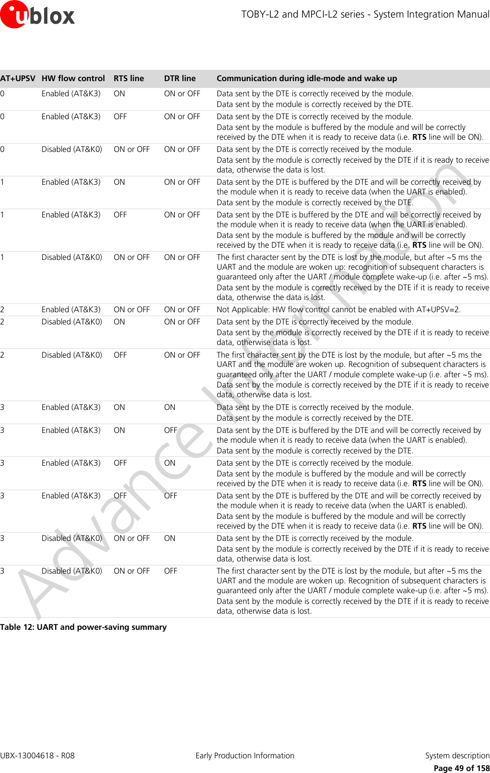
![TOBY-L2 and MPCI-L2 series - System Integration Manual UBX-13004618 - R08 Early Production Information System description Page 50 of 158 AT+UPSV=0: power saving disabled, fixed active-mode The module does not enter low power idle-mode and the UART interface is enabled (data can be sent and received): the CTS line is always held in the ON state after UART initialization. This is the default configuration. AT+UPSV=1: power saving enabled, cyclic idle/active-mode When the AT+UPSV=1 command is issued by the DTE, then the UART is immediately disabled by the module. Afterwards, the UART is enabled again, and the module does not enter low power idle-mode, as following: Periodically, during each paging reception (see section 1.5.1.5), to temporarily receive or send data over the UART, e.g. data buffered by the DTE with HW flow control enabled will be correctly received by the module If the module needs to transmit some data over the UART (e.g. URC), the UART is temporarily enabled If a data call with external context is activated, the UART is kept enabled If the DTE send data with HW flow control disabled, the first character sent causes the UART and module wake-up after ~5 ms: recognition of subsequent characters is guaranteed only after the complete wake-up (see the following subsection “wake up via data reception”) The module automatically enters the low power idle-mode whenever possible but it wakes up to active-mode according to the UART periodic wake up so that the module cyclically enters the low power idle-mode and the active-mode. Additionally, the module wakes up to active-mode according to any required activity related to the network (e.g. for the periodic paging reception described in section 1.5.1.5, or for any other required RF Tx / Rx) or any other required activity related to module functions / interfaces (including the UART itself). When the UART interface is enabled, data can be received. When a character is received, it forces the UART interface to stay enabled for a longer time and it forces the module to stay in the active-mode for a longer time, according to the timeout configured by the second parameter of the +UPSV AT command. The timeout can be set from 40 2G-frames (i.e. 40 x 4.615 ms = 184 ms) up to 65000 2G-frames (i.e. 65000 x 4.615 ms = 300 s). Default value is 2000 2G-frames (i.e. 2000 x 4.615 ms = 9.2 s). Every subsequent character received during the active-mode, resets and restarts the timer; hence the active-mode duration can be extended indefinitely. The hardware flow-control output (CTS line) indicates when the UART interface is enabled (data can be sent and received), as illustrated in Figure 22. time [s]UART disabled~ 20 msUART enabled~9.2 s (default)UART enabledData inputCTS ONCTS OFF2G: 0.45-2.10 s 3G: 0.62-5.10 s LTE: 0.30-2.52 s Figure 22: CTS output pin indicates when module’s UART is enabled (CTS = ON = low level) or disabled (CTS = OFF = high level)](https://usermanual.wiki/u-blox/TOBYL280.System-Integrators-Manual/User-Guide-2664029-Page-50.png)
![TOBY-L2 and MPCI-L2 series - System Integration Manual UBX-13004618 - R08 Early Production Information System description Page 51 of 158 AT+UPSV=2: power saving enabled and controlled by the RTS line This configuration can only be enabled with the module hardware flow control disabled (i.e. AT&K0 setting). The UART interface is immediately disabled after the DTE sets the RTS line to OFF. Afterwards, the UART is enabled again, and the module does not enter low power idle-mode, as following: If an OFF-to-ON transition occurs on the RTS input line, this causes the UART / module wake-up after ~5 ms: recognition of subsequent characters is guaranteed only after the complete wake-up, and the UART is kept enabled as long as the RTS input line is set to ON. If the module needs to transmit some data over the UART (e.g. URC) If a data call with external context is activated If the DTE sends data, the first character sent causes the UART and module wake-up after ~5 ms: the recognition of subsequent characters is guaranteed only after the complete wake-up, and the UART will be then kept enabled after the last data received according to the timeout previously set with the AT+UPSV=1 configuration (see the following subsection “wake up via data reception”) The module automatically enters the low power idle-mode whenever possible but it wakes up to active-mode according to any required activity related to the network (e.g. for the periodic paging reception described in section 1.5.1.5, or for any other required RF transmission / reception) or any other required activity related to the module functions / interfaces (including the UART itself). The hardware flow-control output (CTS line) indicates when the UART interface is enabled (data can be sent and received) as illustrated in Figure 22, even if hardware flow control is disabled with AT+UPSV=2 configuration. AT+UPSV=3: power saving enabled and controlled by the DTR line The UART interface is immediately disabled after the DTE sets the DTR line to OFF. Afterwards, the UART is enabled again, and the module does not enter low power idle-mode, as following: If an OFF-to-ON transition occurs on the DTR input line, this causes the UART / module wake-up after ~5 ms: recognition of subsequent characters is guaranteed only after the complete wake-up, and the UART is kept enabled as long as the DTR input line is set to ON If the module needs to transmit some data over the UART (e.g. URC) If a data call with external context is activated If the DTE sends data, the first character sent causes the UART and module wake-up after ~5 ms: recognition of subsequent characters is guaranteed only after the complete wake-up, and the UART will be then kept enabled after the last data received according to the timeout previously set with the AT+UPSV=1 configuration (see the following subsection “wake up via data reception”) The module automatically enters the low power idle-mode whenever possible but it wakes up to active-mode according to any required activity related to the network (e.g. for the periodic paging reception described in section 1.5.1.5, or for any other required RF signal transmission or reception) or any other required activity related to the functions / interfaces of the module. The AT+UPSV=3 configuration can be enabled regardless the flow control setting on UART. In particular, the HW flow control can be enabled (AT&K3) or disabled (AT&K0) on UART during this configuration. In both cases, the CTS line indicates the UART power saving state as illustrated in Figure 22. When the AT+UPSV=3 configuration is enabled, the DTR input line can still be used by the DTE to control the module behavior according to AT&D command configuration (see u-blox AT commands Manual [3]).](https://usermanual.wiki/u-blox/TOBYL280.System-Integrators-Manual/User-Guide-2664029-Page-51.png)
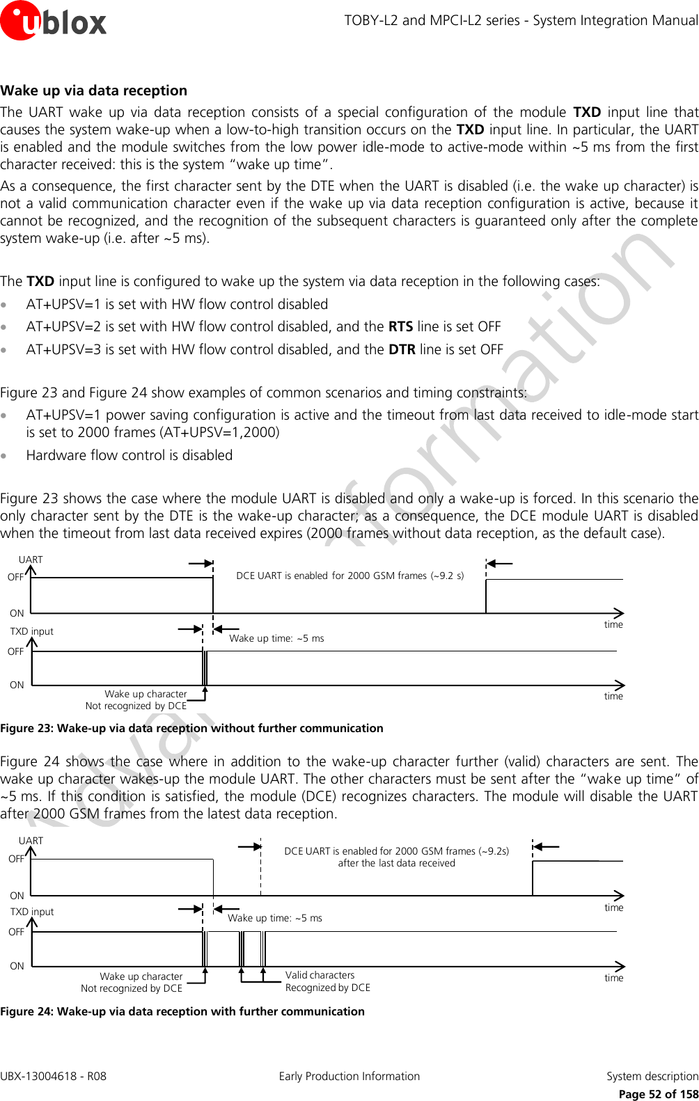
![TOBY-L2 and MPCI-L2 series - System Integration Manual UBX-13004618 - R08 Early Production Information System description Page 53 of 158 The “wake-up via data reception” feature cannot be disabled. In command mode7, if autobauding is enabled and the DTE does not implement HW flow control, the DTE must always send a character to the module before the “AT” prefix set at the beginning of each command line: the first character is ignored if the module is in active-mode, or it represents the wake-up character if the module is in idle-mode. In command mode7, the DTE should always send a dummy “AT” before each command line: the first character is not ignored if the module is in active-mode (i.e. the module replies “OK”), or it represents the wake up character if the module is in low power idle-mode (i.e. the module does not reply). No wake-up character or dummy “AT” is required from the DTE during a data call with external context since the module UART interface continues to be enabled and does not need to be woken-up. Furthermore in data mode7 a dummy “AT” would affect the data communication. Additional considerations If the USB is connected and not suspended, the module is forced to stay in active-mode, therefore the AT+UPSV settings are overruled but they have effect on the UART behavior (they configure UART power saving, so that UART is enabled / disabled according to the AT+UPSV settings). 1.9.2.5 UART multiplexer protocol TOBY-L2 series modules include multiplexer functionality as per 3GPP TS 27.010 [10], on the UART physical link. This is a data link protocol which uses HDLC-like framing and operates between the module (DCE) and the application processor (DTE) and allows a number of simultaneous sessions over the used physical link (UART): the user can concurrently use AT interface on one MUX channel and data communication on another MUX channel. The following virtual channels are defined (for more details, see Mux implementation Application Note [11]): Channel 0: control channel Channel 1 – 5: AT commands / data connection Channel 6: GNSS tunneling (not supported by “00”, “01”, “50” product versions) Channel 7: SIM Access Profile (SAP, not supported by “00”, “01”, “50” product versions) 7 See the u-blox AT Commands Manual [3] for the definition of the interface data mode, command mode and online command mode.](https://usermanual.wiki/u-blox/TOBYL280.System-Integrators-Manual/User-Guide-2664029-Page-53.png)
![TOBY-L2 and MPCI-L2 series - System Integration Manual UBX-13004618 - R08 Early Production Information System description Page 54 of 158 1.9.3 DDC (I2C) interface The I2C bus compatible Display Data Channel interface is not available on the MPCI-L2 series modules, as AssistNow embedded GNSS positioning aiding, CellLocate® positioning through cellular information and custom functions over GPIOs for the integration with u-blox positioning chips / modules. The I2C bus compatible Display Data Channel interface is not supported by the TOBY-L2 series modules “00”, “01” and “50” product versions, as the AssistNow embedded GNSS positioning aiding, CellLocate® positioning through cellular information and custom functions over GPIOs for the integration with u-blox positioning chips / modules. The SDA and SCL pins of TOBY-L2 series modules represent an I2C bus compatible Display Data Channel (DDC) interface for the communication with u-blox GNSS receivers and with other external I2C devices as audio codecs: an I2C master can communicate with more I2C slaves in accordance to the I2C bus specifications [12]. The DDC (I2C) interface is the only one interface dedicated for communication between u-blox cellular module and u-blox positioning receivers. The AT commands interface is not available on the DDC (I2C) interface. The DDC (I2C) interface pads of the module, serial data (SDA) and serial clock (SCL), are open drain output and external pull up resistors must be used conforming to the I2C bus specifications [12]. u-blox has implemented special features in the cellular modules to ease the design effort for the integration of a u-blox cellular module with a u-blox GNSS receiver (details in GNSS Implementation Application Note [13]). Combining a u-blox cellular module with a u-blox GNSS receiver allows designers to full access the GNSS receiver directly via the cellular module: it relays control messages to the GNSS receiver via a dedicated DDC (I2C) interface. A 2nd interface connected to the GNSS receiver is not necessary: AT commands via the AT interfaces of the cellular module (UART, USB) allows a full control of the GNSS receiver from any host processor. u-blox cellular modules feature embedded GNSS aiding that is a set of specific features developed by u-blox to enhance GNSS performance, decreasing Time To First Fix (TTFF), thus allowing to calculate the position in a shorter time with higher accuracy. Additional custom functions over GPIO pins are designed to improve the integration with u-blox GNSS receivers: GNSS receiver power-on/off: “GNSS supply enable” function over the GPIO2 pin improves the positioning receiver power consumption. When the GNSS functionality is not required, the positioning receiver can be completely switched off by the cellular module controlled by the application processor over AT commands The wake up from idle-mode when the GNSS receiver is ready to send data: “GNSS data ready” function over the GPIO3 pin improves the cellular module power consumption. When power saving is enabled in the cellular module by the AT+UPSV command and the GNSS receiver does not send data by the DDC (I2C) interface, the module automatically enters idle-mode whenever possible. With the “GNSS data ready” function the GNSS receiver can indicate to the cellular module that it is ready to send data: the positioning receiver can wake up the cellular module to avoid data loss even if power saving is enabled. The RTC synchronization signal to the GNSS receiver: “GNSS RTC sharing” function over the GPIO4 pin improves GNSS receiver performance, decreasing the Time To First Fix (TTFF), and thus allowing to calculate the position in a shorter time with higher accuracy. When GNSS local aiding is enabled, the cellular module automatically uploads data such as position, time, ephemeris, almanac, health and ionospheric parameter from the positioning receiver into its local memory, and restores this to the GNSS receiver at the next power up of the positioning receiver](https://usermanual.wiki/u-blox/TOBYL280.System-Integrators-Manual/User-Guide-2664029-Page-54.png)
![TOBY-L2 and MPCI-L2 series - System Integration Manual UBX-13004618 - R08 Early Production Information System description Page 55 of 158 1.9.4 Secure Digital Input Output interface (SDIO) Secure Digital Input Output interface is not available on MPCI-L2 series modules. Secure Digital Input Output interface is not supported by TOBY-L2 “00” and “01” product versions. TOBY-L2 series modules include a 4-bit Secure Digital Input Output interface (SDIO_D0, SDIO_D1, SDIO_D2, SDIO_D3, SDIO_CLK, SDIO_CMD) designed to communicate with an external u-blox short range Wi-Fi module: the TOBY-L2 cellular module acts as an SDIO host controller which can communicate over the SDIO bus with a compatible u-blox short range Wi-Fi module acting as SDIO device. The SDIO interface is the only one interface of TOBY-L2 series modules dedicated for communication between the u-blox cellular module and the u-blox short range Wi-Fi module. The AT commands interface is not available on the SDIO interface of TOBY-L2 series modules. The SDIO interface supports 50 MHz bus clock frequency, which allows a data throughput of 200 Mb/s. Combining a u-blox cellular module with a u-blox short range communication module gives designers full access to the Wi-Fi module directly via the cellular module, so that a second interface connected to the Wi-Fi module is not necessary. AT commands via the AT interfaces of the cellular module (UART, USB) allows a full control of the Wi-Fi module from any host processor, because Wi-Fi control messages are relayed to the Wi-Fi module via the dedicated SDIO interface (for more details, see the Wi-Fi AT commands in the u-blox AT Commands Manual [3]). u-blox has implemented special features in the cellular modules to ease the design effort for the integration of a u-blox cellular module with a u-blox short range Wi-Fi module to provide both Bridge and Router functionality (for more details, see the Wi-Fi / Cellular Integration Application Note [14]). Additional custom functions over GPIO pins are designed to improve the integration with u-blox Wi-Fi modules: Wi-Fi enable Switch-on / switch-off the Wi-Fi Wi-Fi reset Reset the Wi-Fi Wi-Fi data ready Cellular module wake-up when the Wi-Fi is ready for sending data over SDIO Wi-Fi power saving Enable/disable the low power mode of the Wi-Fi 32 kHz output Clock for the Wi-Fi 26 MHz output Clock for the Wi-Fi GPIOs are not supported by TOBY-L2 “00”, “01”, and “50” product versions, except for: Wireless Wide Area Network status indication configured on GPIO1 of “00”, “01” product versions Wi-Fi enable function configured on the GPIO1 of “50“ product version GPIOs are not available on MPCI-L2 series modules. 1.10 Audio 1.10.1 Digital audio over I2S interface Digital audio over I2S interface is not available on MPCI-L2 series modules. Digital audio over I2S interface is not supported by TOBY-L2 modules ”00”, “01”, “50” product versions. TOBY-L2 series modules include a 4-wire I2S digital audio interface (I2S_TXD, I2S_RXD, I2S_CLK, I2S_WA) that can be configured by AT command to transfer digital audio data with an external device as an audio codec (for more details see u-blox AT Commands Manual [3]).](https://usermanual.wiki/u-blox/TOBYL280.System-Integrators-Manual/User-Guide-2664029-Page-55.png)
![TOBY-L2 and MPCI-L2 series - System Integration Manual UBX-13004618 - R08 Early Production Information System description Page 56 of 158 1.11 General Purpose Input/Output GPIOs are not supported by TOBY-L2 series modules “00”, “01” and “50” product versions, except for: Wireless Wide Area Network status indication configured on GPIO1 of “00”, “01” product versions Wi-Fi enable function configured on the GPIO1 of “50” product version GPIOs are not available on MPCI-L2 series modules. TOBY-L2 series modules include 14 pins (GPIO1-GPIO6, I2S_TXD, I2S_RXD, I2S_CLK, I2S_WA, DTR, DSR, DCD, RI) that can be configured as General Purpose Input/Output or to provide custom functions via u-blox AT commands (see the u-blox AT Commands Manual [3]), as summarized in Table 13. Function Description Default GPIO Configurable GPIOs Network status indication Network status: registered home network, registered roaming, data transmission, no service GPIO1 GPIO1 GNSS supply enable Enable/disable the supply of u-blox GNSS receiver connected to cellular module GPIO2 GPIO2 GNSS data ready Sense when u-blox GNSS receiver connected to the module is ready for sending data by the DDC (I2C) GPIO3 GPIO3 GNSS RTC sharing Real Time Clock synchronization signal to u-blox GNSS receiver connected to cellular module GPIO4 GPIO4 SIM card detection SIM card physical presence detection GPIO5 GPIO5 SIM card hot insertion/removal SIM card hot insertion/removal -- GPIO5 I2S digital audio interface I2S digital audio interface I2S_RXD, I2S_TXD, I2S_CLK, I2S_WA I2S_RXD, I2S_TXD, I2S_CLK, I2S_WA 26 MHz clock output 26 MHz clock output for an external audio codec or an external Wi-Fi chip/module GPIO6 GPIO6 Wi-Fi enable Enable/disable the supply of the external Wi-Fi chip or module connected to the cellular module -- GPIO1, GPIO4, DSR Wi-Fi data ready Sense when the external Wi-Fi chip/module connected to the cellular module is ready for sending data by the SDIO, waking up the cellular module from low power idle mode -- GPIO3, DTR Wi-Fi reset Reset the external Wi-Fi chip or module connected to the cellular module -- GPIO3, DCD Wi-Fi power saving Enable/disable the low power mode of the external Wi-Fi chip/module connected to the cellular module -- GPIO2, RI 32 kHz clock output 32 kHz clock output for an external Wi-Fi chip or module -- GPIO6 Antenna tuning 4-bit tunable antenna control signals mapping the actual operating RF band over a 4-pin interface provided for the implementation of external antenna tuning solutions -- I2S_RXD, I2S_TXD, I2S_CLK, I2S_WA DSR, DTR, DCD, RI DSR UART data set ready output DSR DSR DTR UART data terminal ready input DTR DTR DCD UART data carrier detect output DCD DCD RI UART ring indicator output RI RI General purpose input Input to sense high or low digital level -- All General purpose output Output to set the high or the low digital level -- All Pin disabled Tri-state with an internal active pull-down enabled -- All Table 13: TOBY-L2 series GPIO custom functions configuration](https://usermanual.wiki/u-blox/TOBYL280.System-Integrators-Manual/User-Guide-2664029-Page-56.png)
![TOBY-L2 and MPCI-L2 series - System Integration Manual UBX-13004618 - R08 Early Production Information System description Page 57 of 158 1.12 Mini PCIe specific signals (W_DISABLE#, LED_WWAN#) Mini PCI Express specific signals (W_DISABLE#, LED_WWAN#) are not available on TOBY-L2 series. MPCI-L2 series modules include the W_DISABLE# active-low input signal to disable the radio operations as specified by the PCI Express Mini Card Electromechanical Specification [15]. As described in Figure 25, the W_DISABLE# input is equipped with an internal pull-up to the 3.3Vaux supply. The W_DISABLE# input detailed electrical characteristics are described in the MPCI-L2 series Data Sheet [2]. Baseband Processor20W_DISABLE#MPCI-L2 series3.3VauxW_DISABLE#22k Figure 25: MPCI-L2 series modules W_DISABLE# input circuit description MPCI-L2 series modules include the LED_WWAN# active-low open drain output to provide the Wireless Wide Area Network status indication as specified by the PCI Express Mini Card Electromechanical Specification [15]. For more electrical characteristics details see the MPCI-L2 Data Sheet [2]. 1.13 Reserved pins (RSVD) Pins reserved for future use, marked as RSVD, are not available on MPCI-L2 series. TOBY-L2 series modules have pins reserved for future use, marked as RSVD: they can all be left unconnected on the application board, except the RSVD pin number 6 that must be externally connected to ground. 1.14 Not connected pins (NC) Pins internally not connected, marked as NC, are not available on TOBY-L2 series. MPCI-L2 series modules have pins internally not connected, marked as NC: they can be left unconnected or they can be connected on the application board according to any application requirement, given that none function is provided by the modules over these pins.](https://usermanual.wiki/u-blox/TOBYL280.System-Integrators-Manual/User-Guide-2664029-Page-57.png)
![TOBY-L2 and MPCI-L2 series - System Integration Manual UBX-13004618 - R08 Early Production Information System description Page 58 of 158 1.15 System features 1.15.1 Network indication Network status indication over GPIO1 is not available on MPCI-L2 series modules which include the LED_WWAN# active-low open drain output to provide the Wireless Wide Area Network status indication as specified by the PCI Express Mini Card Electromechanical Specification [15]. GPIOs are not supported by TOBY-L2 modules “00”, “01”, “50” product versions, but the Wireless Wide Area Network status indication is by default configured on the GPIO1 of “00”, “01” product version. The GPIO1 can be configured by the AT+UGPIOC command (for further details see the u-blox AT Commands Manual [3]), to indicate network status as described below: No service (no network coverage or not registered) Registered 2G / 3G / LTE home network Registered 2G / 3G / LTE visitor network (roaming) Call enabled (RF data transmission / reception) 1.15.2 Antenna supervisor Antenna supervisor (i.e. antenna detection) is not available on MPCI-L2 series. Antenna supervisor (i.e. antenna detection) is not supported by TOBY-L2 series modules “00”, “01” and “50” product versions. The antenna detection function provided by the ANT_DET pin is based on an ADC measurement as optional feature that can be implemented if the application requires it. The antenna supervisor is forced by the +UANTR AT command (see the u-blox AT Commands Manual [3] for more details). The requirements to achieve antenna detection functionality are the following: an RF antenna assembly with a built-in resistor (diagnostic circuit) must be used an antenna detection circuit must be implemented on the application board See section 1.7.2 for detailed antenna detection interface functional description and see section 2.4.2 for detection circuit on application board and diagnostic circuit on antenna assembly design-in guidelines. 1.15.3 Jamming detection Congestion detection (i.e. jamming detection) is not supported by “00”, “01” and “50” product versions. In real network situations modules can experience various kind of out-of-coverage conditions: limited service conditions when roaming to networks not supporting the specific SIM, limited service in cells which are not suitable or barred due to operators’ choices, no cell condition when moving to poorly served or highly interfered areas. In the latter case, interference can be artificially injected in the environment by a noise generator covering a given spectrum, thus obscuring the operator’s carriers entitled to give access to the LTE/3G/2G service. The congestion (i.e. jamming) detection feature can be enabled and configured by the +UCD AT command: the feature consists of detecting an anomalous source of interference and signaling the start and stop of such conditions to the host application processor with an unsolicited indication, which can react appropriately by e.g. switching off the radio transceiver of the module (i.e. configuring the module in “airplane mode” by means of the +CFUN AT command) in order to reduce power consumption and monitoring the environment at constant periods (for more details see the u-blox AT Commands Manual [3]).](https://usermanual.wiki/u-blox/TOBYL280.System-Integrators-Manual/User-Guide-2664029-Page-58.png)
![TOBY-L2 and MPCI-L2 series - System Integration Manual UBX-13004618 - R08 Early Production Information System description Page 59 of 158 1.15.4 IP modes of operation IP modes of operation refer to the TOBY-L2 and MPCI-L2 series modules configuration related to the network IP termination and network interfaces settings in general. IP modes of operation are the following: Bridge mode: In bridge mode the module acts as a cellular modem dongle connected to the host over serial interface. The IP termination of the network is placed on the host IP stack. The module is configured as a bridge which means the network IP address is assigned to the host (host IP termination). Router mode: In router mode the module acts as a cellular modem router which means the IP termination of the network is placed on the internal IP stack of the module (on-target IP termination). In particular, in this configuration the application processor belongs to a private network and is not aware of the mobile connectivity setup of the module. For more details about IP modes of operation see the u-blox AT Commands Manual [3]. 1.15.5 Dual stack IPv4/IPv6 TOBY-L2 and MPCI-L2 series support both Internet Protocol version 4 and Internet Protocol version 6 in parallel. For more details about dual stack IPv4/IPv6 see the u-blox AT Commands Manual [3]. 1.15.6 TCP/IP and UDP/IP Embedded TCP/IP and UDP/IP stack as well as Direct Link mode are not supported by the “00” and “50” product versions. TOBY-L2 and MPCI-L2 series modules provide embedded TCP/IP and UDP/IP protocol stack: a PDP context can be configured, established and handled via the data connection management packet switched data commands. TOBY-L2 and MPCI-L2 series modules provide Direct Link mode to establish a transparent end-to-end communication with an already connected TCP or UDP socket via serial interfaces (USB, UART). In Direct Link mode, data sent to the serial interface from an external application processor is forwarded to the network and vice-versa. For more details about embedded TCP/IP and UDP/IP functionalities see the u-blox AT Commands Manual [3]. 1.15.7 FTP Embedded FTP services as well as Direct Link mode are not supported by “00” and “50” product versions. TOBY-L2 and MPCI-L2 series provide embedded File Transfer Protocol (FTP) services. Files are read and stored in the local file system of the module. FTP files can also be transferred using FTP Direct Link: FTP download: data coming from the FTP server is forwarded to the host processor via USB / UART serial interfaces (for FTP without Direct Link mode the data is always stored in the module’s Flash File System) FTP upload: data coming from the host processor via USB / UART serial interface is forwarded to the FTP server (for FTP without Direct Link mode the data is read from the module’s Flash File System) When Direct Link is used for a FTP file transfer, only the file content pass through USB / UART serial interface, whereas all the FTP commands handling is managed internally by the FTP application. For more details about embedded FTP functionalities see u-blox AT Commands Manual [3].](https://usermanual.wiki/u-blox/TOBYL280.System-Integrators-Manual/User-Guide-2664029-Page-59.png)
![TOBY-L2 and MPCI-L2 series - System Integration Manual UBX-13004618 - R08 Early Production Information System description Page 60 of 158 1.15.8 HTTP Embedded HTTP services are not supported by “00” and “50” product versions. TOBY-L2 and MPCI-L2 series modules provide the embedded Hyper-Text Transfer Protocol (HTTP) services via AT commands for sending requests to a remote HTTP server, receiving the server response and transparently storing it in the module’s Flash File System (FFS). For more details about embedded HTTP functionalities see the u-blox AT Commands Manual [3]. 1.15.9 SSL Embedded Transport Layer Security (TLS) / Secure Sockets Layer (SSL) protocols are not supported by the “00”, “01” and “50” product versions. TOBY-L2 and MPCI-L2 series modules provide the Transport Layer Security (TLS) / Secure Sockets Layer (SSL) encryption protocols to enable security over the FTP and HTTP protocols via AT commands, implementing Secure File Transfer Protocol (FTPS, i.e. FTP with TLS / SSL encryption) and Secure Hyper-Text Transfer Protocol (HTTPS, i.e. HTTP with TLS / SSL encryption) services. For more details about embedded TLS / SSL functionalities see the u-blox AT Commands Manual [3]. 1.15.10 AssistNow clients and GNSS integration AssistNow clients and u-blox GNSS receiver integration are not available on the MPCI-L2 series modules. AssistNow clients and u-blox GNSS receiver integration are not supported by the TOBY-L2 series modules “00”, “01” and “50” product versions. For customers using u-blox GNSS receivers, TOBY-L2 series cellular modules feature embedded AssistNow clients. AssistNow A-GPS provides better GNSS performance and faster Time-To-First-Fix. The clients can be enabled and disabled with an AT command (see the u-blox AT Commands Manual [3]). TOBY-L2 series cellular modules act as a stand-alone AssistNow client, making AssistNow available with no additional requirements for resources or software integration on an external host micro controller. Full access to u-blox GNSS receivers is available via the TOBY-L2 series cellular module, through the DDC (I2C) interface, while the available GPIOs can handle the positioning chipset / module power-on/off. This means that cellular module and GNSS receiver can be controlled through a single serial port from any host processor. 1.15.11 Hybrid positioning and CellLocate® Hybrid positioning and CellLocate® are not available on MPCI-L2 series. Hybrid positioning and CellLocate® are not supported by the TOBY-L2 series modules “00”, “01” and “50” product versions. Although GNSS is a widespread technology, its reliance on the visibility of extremely weak GNSS satellite signals means that positioning is not always possible. Especially difficult environments for GNSS are indoors, in enclosed or underground parking garages, as well as in urban canyons where GNSS signals are blocked or jammed by multipath interference. The situation can be improved by augmenting GNSS receiver data with cellular network information to provide positioning information even when GNSS reception is degraded or absent. This additional information can benefit numerous applications.](https://usermanual.wiki/u-blox/TOBYL280.System-Integrators-Manual/User-Guide-2664029-Page-60.png)
![TOBY-L2 and MPCI-L2 series - System Integration Manual UBX-13004618 - R08 Early Production Information System description Page 63 of 158 The use of hybrid positioning requires a connection via the DDC (I2C) bus between the TOBY-L2 series cellular module and the u-blox GNSS receiver (see sections 1.9.3 and 2.6.3). See GNSS Implementation Application Note [13] for the complete description of the feature. u-blox is extremely mindful of user privacy. When a position is sent to the CellLocate® server u-blox is unable to track the SIM used or the specific device. 1.15.12 Wi-Fi integration u-blox short range communication Wi-Fi modules integration is not available for MPCI-L2 series modules. u-blox short range communication Wi-Fi modules integration is not supported by the TOBY-L2 series modules “00” and “01” product versions. Full access to u-blox short range communication Wi-Fi modules is available through a dedicated SDIO interface (see sections 1.9.4 and 2.6.4). This means that combining a TOBY-L2 series cellular module with a u-blox short range communication module gives designers full access to the Wi-Fi module directly via the cellular module, so that a second interface connected to the Wi-Fi module is not necessary. AT commands via the AT interfaces of the cellular module (UART, USB) allows a full control of the Wi-Fi module from any host processor, because Wi-Fi control messages are relayed to the Wi-Fi module via the dedicated SDIO interface (for more details, see the Wi-Fi AT commands in the u-blox AT Commands Manual [3]). All the management software for Wi-Fi module operations runs inside the cellular module in addition to those required for cellular-only operation: Wi-Fi driver, Web User Interface (WebUI), Connection Config Manager. For more details, see the Wi-Fi / Cellular Integration Application Note [14]. 1.15.13 Firmware update Over AT (FOAT) This feature allows upgrading the module firmware over USB / UART serial interfaces, using AT commands. The +UFWUPD AT command triggers a reboot followed by the upgrade procedure at specified a baud rate A special boot loader on the module performs firmware installation, security verifications and module reboot Firmware authenticity verification is performed via a security signature during the download. The firmware is then installed, overwriting the current version. In case of power loss during this phase, the boot loader detects a fault at the next wake-up, and restarts the firmware download. After completing the upgrade, the module is reset again and wakes-up in normal boot For more details about Firmware update Over AT procedure see the Firmware Update Application Note [4] and the u-blox AT Commands Manual [3], +UFWUPD AT command. 1.15.14 Firmware update Over The Air (FOTA) Firmware update Over The Air (FOTA) is not supported by “00” and “50” product versions. This feature allows upgrading the module firmware over the LTE/3G/2G air interface. In order to reduce the amount of data to be transmitted over the air, the implemented FOTA feature requires downloading only a “delta file” instead of the full firmware. The delta file contains only the differences between the two firmware versions (old and new), and is compressed. The firmware update procedure can be triggered using dedicated AT command with the delta file stored in the module file system via over the air FTP. For more details about Firmware update Over The Air procedure see the Firmware Update Application Note [4] and the u-blox AT Commands Manual [3], +UFWINSTALL AT command.](https://usermanual.wiki/u-blox/TOBYL280.System-Integrators-Manual/User-Guide-2664029-Page-63.png)
![TOBY-L2 and MPCI-L2 series - System Integration Manual UBX-13004618 - R08 Early Production Information System description Page 64 of 158 1.15.15 In-band Modem (eCall / ERA-GLONASS) In-band modem for eCall / ERA-GLONASS emergency applications is not supported by TOBY-L2 series modules “00”, “01”, and “50” product versions and by MPCI-L2 series modules. In-band Modem solution for eCall and ERA-GLONASS emergency call applications over cellular networks is implemented according to 3GPP TS 26.267 [16], BS EN 16062:2011 [17] and ETSI TS 122 101 [18] specifications. eCall (European) and ERA-GLONASS (Russian) are initiatives to combine mobile communications and satellite positioning to provide rapid assistance to motorists in the event of a collision, implementing automated emergency response system based the first on GPS the latter on GLONASS positioning system. When activated, the in-vehicle systems (IVS) automatically initiate an emergency call carrying both voice and data (including location data) directly to the nearest Public Safety Answering Point (PSAP) to determine whether rescue services should be dispatched to the known position. Figure 26: eCall and ERA-GLONASS automated emergency response systems diagram flow For more details regarding the In-band Modem solution for the European eCall and the Russian ERA-GLONASS emergency call applications, see the u-blox eCall / ERA-GLONASS Application Note [19]. 1.15.16 SIM Access Profile (SAP) SIM Access Profile (SAP) is not supported by TOBY-L2 “00”, “01”, and “50” product versions or by MPCI-L2 series modules. SIM access profile (SAP) feature allows accessing and using a remote SIM card / chipping instead of the local SIM directly connected to the module SIM interface. A dedicated SAP channel over USB and a dedicated multiplexed SAP channel over UART are implemented for communication with the remote SIM card/chip. Communication between TOBY-L2 series module and the remote SIM is conformed to client-server paradigm: The module is the SAP client establishing a connection and performing data exchange to a SAP server directly connected to the remote SIM that is used by the module for LTE/3G/2G network-related operations. The SAP communication protocol is based on the SIM Access Profile Interoperability Specification [20]. A typical application using the SAP feature is the scenario where a device such as an embedded car-phone with an integrated TOBY-L2 series module uses a remote SIM included in an external user device (e.g. a simple SIM card reader or a portable phone), which is brought into the car. The car-phone accesses the LTE/3G/2G network using the remote SIM in the external device.](https://usermanual.wiki/u-blox/TOBYL280.System-Integrators-Manual/User-Guide-2664029-Page-64.png)
![TOBY-L2 and MPCI-L2 series - System Integration Manual UBX-13004618 - R08 Early Production Information System description Page 65 of 158 TOBY-L2 series modules, acting as an SAP client, can be connected to an SAP server by a completely wired connection, as shown in Figure 27. Device including TOBY-L2LTE/3G/2G InterfaceLocal SIM(optional)TOBY-L2SAP ClientApplicationProcessorDevice including SIMSAP Serial InterfaceRemote SIMMobileEquipmentSAP ServerSAP Serial Interface(SAP channel over USB or UART) Figure 27: Remote SIM access via completely wired connection As stated in the SIM Access Profile Interoperability Specification [20], the SAP client can be connected to the SAP server by means of a Bluetooth wireless link, using additional Bluetooth transceivers. In this case, the application processor wired to TOBY-L2 series module establishes and controls the Bluetooth connection using the SAP profile, and routes data received over a serial interface channel to data transferred over a Bluetooth interface and vice versa, as shown in Figure 28. Device including TOBY-L2SAP Serial Interface(SAP channel over USB or UART)LTE/3G/2G InterfaceLocal SIM(optional)TOBY-L2SAP ClientApplicationProcessorSAP Bluetooth InterfaceBluetoothTransceiverDevice including SIMRemote SIMMobileEquipmentSAP ServerBluetoothTransceiver Figure 28: Remote SIM access via Bluetooth and wired connection The application processor can start an SAP connection negotiation between TOBY-L2 series module SAP client and an SAP server using custom AT command (for more details see u-blox AT Commands Manual [3]). While the connection with the SAP server is not fully established, the TOBY-L2 series module continues to operate with the attached (local) SIM, if present. Once the connection is established and negotiated, the module performs a detach operation from the local SIM followed by an attach operation to the remote one. Then the remotely attached SIM is used for any LTE/3G/2G network operation. URC indications are provided to inform the user about the state of both the local and remote SIM. The insertion and the removal of the local SIM card are notified if a proper card presence detection circuit using the GPIO5 of TOBY-L2 series modules is implemented as shown in section 2.5, and if the related “SIM card detection” and “SIM hot insertion/removal” functions described in section 1.8.2 are enabled by AT commands (for more details see u-blox AT Commands Manual [3]). Upon SAP deactivation, the TOBY-L2 series modules perform a detach operation from the remote SIM followed by an attach operation to the local one, if present.](https://usermanual.wiki/u-blox/TOBYL280.System-Integrators-Manual/User-Guide-2664029-Page-65.png)
![TOBY-L2 and MPCI-L2 series - System Integration Manual UBX-13004618 - R08 Early Production Information System description Page 66 of 158 1.15.17 Smart temperature management Smart temperature management is not supported by “00”, “01”, and “50” product versions. Cellular modules – independent of the specific model – always have a well defined operating temperature range. This range should be respected to guarantee full device functionality and long life span. Nevertheless there are environmental conditions that can affect operating temperature, e.g. if the device is located near a heating/cooling source, if there is/isn’t air circulating, etc. The module itself can also influence the environmental conditions; such as when it is transmitting at full power. In this case its temperature increases very quickly and can raise the temperature nearby. The best solution is always to properly design the system where the module is integrated. Nevertheless an extra check/security mechanism embedded into the module is a good solution to prevent operation of the device outside of the specified range. Smart Temperature Supervisor (STS) The Smart Temperature Supervisor is activated and configured by a dedicated AT+USTS command. See the u-blox AT Commands Manual [3] for more details. The cellular module measures the internal temperature (Ti) and its value is compared with predefined thresholds to identify the actual working temperature range. Temperature measurement is done inside the cellular module: the measured value could be different from the environmental temperature (Ta). Warningareat-1 t+1 t+2t-2Valid temperature rangeSafeareaDangerousarea Dangerousarea Warningarea Figure 29: Temperature range and limits The entire temperature range is divided into sub-regions by limits (see Figure 29) named t-2, t-1, t+1 and t+2. Within the first limit, (t-1 < Ti < t+1), the cellular module is in the normal working range, the Safe Area In the Warning Area, (t-2 < Ti < t.1) or (t+1 < Ti < t+2), the cellular module is still inside the valid temperature range, but the measured temperature approaches the limit (upper or lower). The module sends a warning to the user (through the active AT communication interface), which can take, if possible, the necessary actions to return to a safer temperature range or simply ignore the indication. The module is still in a valid and good working condition Outside the valid temperature range, (Ti < t-2) or (Ti > t+2), the device is working outside the specified range and represents a dangerous working condition. This condition is indicated and the device shuts down to avoid damage For security reasons the shutdown is suspended in case an emergency call in progress. In this case the device will switch off at call termination. The user can decide at anytime to enable/disable the Smart Temperature Supervisor feature. If the feature is disabled there is no embedded protection against disallowed temperature conditions.](https://usermanual.wiki/u-blox/TOBYL280.System-Integrators-Manual/User-Guide-2664029-Page-66.png)
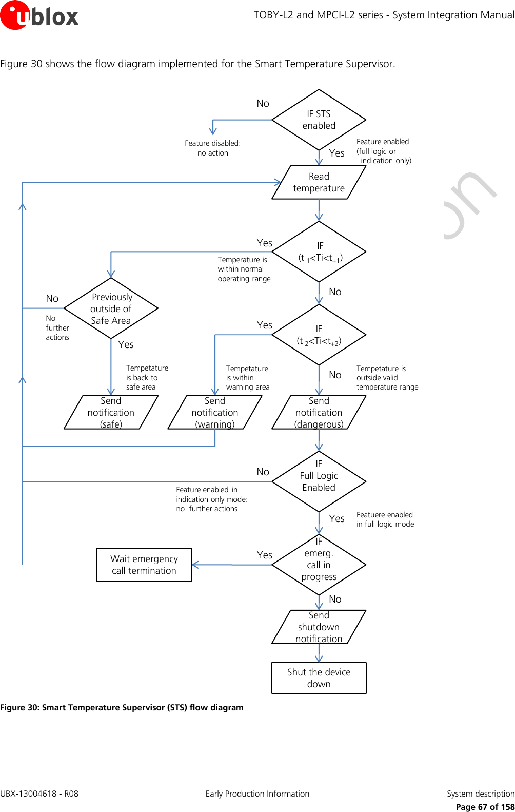
![TOBY-L2 and MPCI-L2 series - System Integration Manual UBX-13004618 - R08 Early Production Information System description Page 68 of 158 Threshold Definitions When the application of cellular module operates at extreme temperatures with Smart Temperature Supervisor enabled, the user should note that outside the valid temperature range the device will automatically shut down as described above. The input for the algorithm is always the temperature measured within the cellular module (Ti, internal). This value can be higher than the working ambient temperature (Ta, ambient), as (for example) during transmission at maximum power a significant fraction of DC input power is dissipated as heat This behavior is partially compensated by the definition of the upper shutdown threshold (t+2) that is slightly higher than the declared environmental temperature limit. The sensor measures board temperature inside the shields, which can differ from ambient temperature. 1.15.18 Power saving The power saving configuration is by default disabled, but it can be enabled using the AT+UPSV command (for the complete description of the AT+UPSV command, see the u-blox AT Commands Manual [3]). When power saving is enabled, the module automatically enters the low power idle-mode whenever possible, reducing current consumption (see section 1.5.1.5, TOBY-L2 Data Sheet [1] and MPCI-L2 Data Sheet [2]). During the low power idle-mode, the module is not ready to communicate with an external device, as it is configured to reduce power consumption. The module wakes up from low power idle-mode to active-mode in the following events: Automatic periodic monitoring of the paging channel for the reception of the paging block sent by the base station according to network conditions (see section 1.5.1.5) The connected USB host forces a remote wakeup of the module as USB device (see section 1.9.1.4) Automatic periodic enable of the UART interface to receive / send data, with AT+UPSV=1 (see 1.9.2.4) Data received on UART interface, with HW flow control disabled and AT+UPSV=1 (see 1.9.2.4) RTS input set ON by the host DTE, with HW flow control disabled and AT+UPSV=2 (see 1.9.2.4) DTR input set ON by the host DTE, with AT+UPSV=3 (see 1.9.2.4) The connected SDIO device forces a wakeup of the module as SDIO host (see 1.9.4) A preset RTC alarm occurs (see u-blox AT Commands Manual [3], AT+CALA) For the definition and the description of TOBY-L2 and MPCI-L2 series modules operating modes, including the events forcing transitions between the different operating modes, see the section 1.4.](https://usermanual.wiki/u-blox/TOBYL280.System-Integrators-Manual/User-Guide-2664029-Page-68.png)
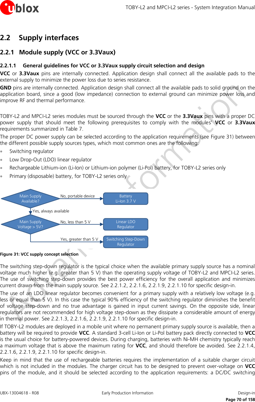
![TOBY-L2 and MPCI-L2 series - System Integration Manual UBX-13004618 - R08 Early Production Information Design-in Page 71 of 158 charger is the typical choice when the charging source has an high nominal voltage (e.g. ~12 V), whereas a linear charger is the typical choice when the charging source has a relatively low nominal voltage (~5 V). If both a permanent primary supply / charging source (e.g. ~12 V) and a rechargeable back-up battery (e.g. 3.7 V Li-Pol) are available at the same time in the application as possible supply source, then a proper charger / regulator with integrated power path management function can be selected to supply the module while simultaneously and independently charging the battery. See 2.2.1.7, 2.2.1.8 and 2.2.1.6, 2.2.1.9, 2.2.1.10 for specific design-in. The use of a primary (not rechargeable) battery is in general uncommon, but appropriate parts can be selected given that the most cells available are seldom capable of delivering the maximum current specified in TOBY-L2 series Data Sheet [1] during connected-mode. Carefully evaluate the usage of super-capacitors as supply source since aging and temperature conditions significantly affect the actual capacitor characteristics. See 2.2.1.5 and 2.2.1.6, 2.2.1.9, 2.2.1.10 for specific design-in. Rechargeable 3-cell Li-Ion or Li-Pol and Ni-MH chemistry batteries reach a maximum voltage that is above the maximum rating for the 3.3Vaux supply of MPCI-L2 modules, and should therefore be avoided. The use of rechargeable, not-rechargeable battery or super-capacitors is very uncommon for Mini PCI Express applications, so that these supply sources types are not considered for MPCI-L2 modules. The usage of more than one DC supply at the same time should be carefully evaluated: depending on the supply source characteristics, different DC supply systems can result as mutually exclusive. The following sections highlight some design aspects for each of the supplies listed above providing application circuit design-in compliant with the module VCC requirements summarized in Table 7. 2.2.1.2 Guidelines for VCC or 3.3Vaux supply circuit design using a switching regulator The use of a switching regulator is suggested when the difference from the available supply rail to the VCC or the 3.3Vaux value is high, since switching regulators provide good efficiency transforming a 12 V or greater voltage supply to the typical 3.8 V value of the VCC supply or the typical 3.3 V value of the 3.3Vaux supply. The characteristics of the switching regulator connected to VCC or 3.3Vaux pins should meet the following prerequisites to comply with the module VCC or 3.3Vaux requirements summarized in Table 7: Power capability: the switching regulator with its output circuit must be capable of providing a voltage value to the VCC or 3.3Vaux pins within the specified operating range and must be capable of delivering to VCC or 3.3Vaux pins the maximum peak / pulse current consumption during Tx burst at maximum Tx power specified in the TOBY-L2 series Data Sheet [1] or in the MPCI-L2 series Data Sheet [2]. Low output ripple: the switching regulator together with its output circuit must be capable of providing a clean (low noise) VCC or 3.3Vaux voltage profile. High switching frequency: for best performance and for smaller applications it is recommended to select a switching frequency ≥ 600 kHz (since L-C output filter is typically smaller for high switching frequency). The use of a switching regulator with a variable switching frequency or with a switching frequency lower than 600 kHz must be carefully evaluated since this can produce noise in the VCC or 3.3Vaux voltage profile and therefore negatively impact LTE/3G/2G modulation spectrum performance. An additional L-C low-pass filter between the switching regulator output to VCC or 3.3Vaux supply pins can mitigate the ripple at the input of the module, but adds extra voltage drop due to resistive losses on series inductors. PWM mode operation: it is preferable to select regulators with Pulse Width Modulation (PWM) mode. While in connected-mode, the Pulse Frequency Modulation (PFM) mode and PFM/PWM modes transitions must be avoided to reduce the noise on the VCC or 3.3Vaux voltage profile. Switching regulators can be used that are able to switch between low ripple PWM mode and high ripple PFM mode, provided that the mode transition occurs when the module changes status from the idle/active-modes to connected-mode. It is permissible to use a regulator that switches from the PWM mode to the burst or PFM mode at an appropriate current threshold.](https://usermanual.wiki/u-blox/TOBYL280.System-Integrators-Manual/User-Guide-2664029-Page-71.png)
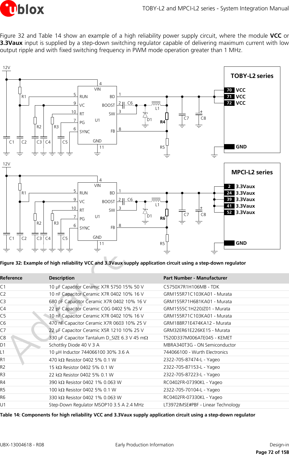
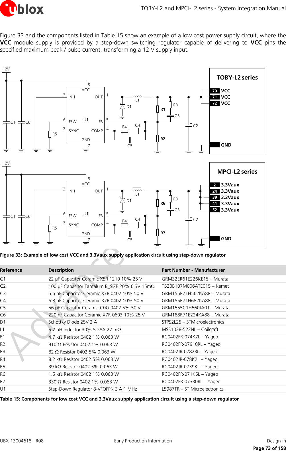
![TOBY-L2 and MPCI-L2 series - System Integration Manual UBX-13004618 - R08 Early Production Information Design-in Page 74 of 158 2.2.1.3 Guidelines for VCC or 3.3Vaux supply circuit design using a Low Drop-Out linear regulator The use of a linear regulator is suggested when the difference from the available supply rail and the VCC or the 3.3Vaux value is low. The linear regulators provide high efficiency when transforming a 5 VDC supply to a voltage value within the module VCC or 3.3Vaux normal operating range. The characteristics of the Low Drop-Out (LDO) linear regulator connected to VCC or 3.3Vaux pins should meet the following prerequisites to comply with the module VCC or 3.3Vaux requirements summarized in Table 7: Power capabilities: the LDO linear regulator with its output circuit must be capable of providing a voltage value to the VCC or 3.3Vaux pins within the specified operating range and must be capable of delivering to VCC or 3.3Vaux pins the maximum peak / pulse current consumption during Tx burst at maximum Tx power specified in TOBY-L2 series Data Sheet [1] or in MPCI-L2 series Data Sheet [2]. Power dissipation: the power handling capability of the LDO linear regulator must be checked to limit its junction temperature to the maximum rated operating range (i.e. check the voltage drop from the max input voltage to the minimum output voltage to evaluate the power dissipation of the regulator). Figure 34 and the components listed in Table 16 show an example of a power supply circuit, where the VCC or 3.3Vaux module supply is provided by an LDO linear regulator capable of delivering the required current, with proper power handling capability. It is recommended to configure the LDO linear regulator to generate a voltage supply value slightly below the maximum limit of the module VCC or 3.3Vaux normal operating range (e.g. ~4.1 V for the VCC and ~3.44 V for the 3.3Vaux as in the circuits described in Figure 34 and Table 16). This reduces the power on the linear regulator and improves the thermal design of the circuit. 5VC1 R1IN OUTADJGND12453C2R2R3U1SHDNTOBY-L2 series71 VCC72 VCC70 VCCGNDC35VC1 R1IN OUTADJGND12453C2R4R5U1SHDNMPCI-L2 seriesGNDC324 3.3Vaux39 3.3Vaux23.3Vaux41 3.3Vaux52 3.3Vaux Figure 34: Suggested schematic design for the VCC and 3.3Vaux supply application circuit using an LDO linear regulator Reference Description Part Number - Manufacturer C1, C2 10 µF Capacitor Ceramic X5R 0603 20% 6.3 V GRM188R60J106ME47 - Murata C3 330 µF Capacitor Tantalum D_SIZE 6.3 V 45 m T520D337M006ATE045 - KEMET R1 47 k Resistor 0402 5% 0.1 W RC0402JR-0747KL - Yageo Phycomp R2 9.1 k Resistor 0402 5% 0.1 W RC0402JR-079K1L - Yageo Phycomp R3 3.9 k Resistor 0402 5% 0.1 W RC0402JR-073K9L - Yageo Phycomp R4 3.3 k Resistor 0402 5% 0.1 W RC0402JR-073K3L - Yageo Phycomp R5 1.8 k Resistor 0402 5% 0.1 W RC0402JR-071K8L - Yageo Phycomp U1 LDO Linear Regulator ADJ 3.0 A LT1764AEQ#PBF - Linear Technology Table 16: Suggested components for VCC and 3.3Vaux supply application circuit using an LDO linear regulator](https://usermanual.wiki/u-blox/TOBYL280.System-Integrators-Manual/User-Guide-2664029-Page-74.png)
![TOBY-L2 and MPCI-L2 series - System Integration Manual UBX-13004618 - R08 Early Production Information Design-in Page 75 of 158 Figure 35 and the components listed in Table 17 show an example of a low cost power supply circuit, where the VCC module supply is provided by an LDO linear regulator capable of delivering the specified highest peak / pulse current, with proper power handling capability. The regulator described in this example supports a limited input voltage range and it includes internal circuitry for current and thermal protection. It is recommended to configure the LDO linear regulator to generate a voltage supply value slightly below the maximum limit of the module VCC normal operating range (e.g. ~4.1 V as in the circuit described in Figure 35 and Table 17). This reduces the power on the linear regulator and improves the whole thermal design of the supply circuit. 5VC1IN OUTADJGND12453C2R1R2U1ENTOBY-L2 series71 VCC72 VCC70 VCCGNDC35VC1IN OUTADJGND12453C2R3R4U1ENMPCI-L2 seriesGNDC324 3.3Vaux39 3.3Vaux23.3Vaux41 3.3Vaux52 3.3Vaux Figure 35: Suggested schematic design for the VCC and 3.3Vaux supply application circuit using an LDO linear regulator Reference Description Part Number - Manufacturer C1, C2 10 µF Capacitor Ceramic X5R 0603 20% 6.3 V GRM188R60J106ME47 - Murata C3 330 µF Capacitor Tantalum D_SIZE 6.3 V 45 m T520D337M006ATE045 - KEMET R1 27 k Resistor 0402 5% 0.1 W RC0402JR-0727KL - Yageo Phycomp R2 4.7 k Resistor 0402 5% 0.1 W RC0402JR-074K7L - Yageo Phycomp R3 12 k Resistor 0402 5% 0.1 W RC0402JR-0712KL - Yageo Phycomp R4 2.7 k Resistor 0402 5% 0.1 W RC0402JR-072K7L - Yageo Phycomp U1 LDO Linear Regulator ADJ 3.0 A LP38501ATJ-ADJ/NOPB - Texas Instrument Table 17: Suggested components for VCC voltage supply application circuit using an LDO linear regulator 2.2.1.4 Guidelines for VCC supply circuit design using a rechargeable Li-Ion or Li-Pol battery Rechargeable Li-Ion or Li-Pol batteries connected to the VCC pins should meet the following prerequisites to comply with the module VCC requirements summarized in Table 7: Maximum pulse and DC discharge current: the rechargeable Li-Ion battery with its related output circuit connected to the VCC pins must be capable of delivering a pulse current as the maximum peak current consumption during Tx burst at maximum Tx power specified in TOBY-L2 series Data Sheet [1] and must be capable of extensively delivering a DC current as the maximum average current consumption specified in TOBY-L2 series Data Sheet [1]. The maximum discharge current is not always reported in battery data sheets, but the maximum DC discharge current is typically almost equal to the battery capacity in Amp-hours divided by 1 hour. DC series resistance: the rechargeable Li-Ion battery with its output circuit must be capable of avoiding a VCC voltage drop below the operating range summarized in Table 7 during transmit bursts.](https://usermanual.wiki/u-blox/TOBYL280.System-Integrators-Manual/User-Guide-2664029-Page-75.png)
![TOBY-L2 and MPCI-L2 series - System Integration Manual UBX-13004618 - R08 Early Production Information Design-in Page 76 of 158 2.2.1.5 Guidelines for VCC supply circuit design using a primary (disposable) battery The characteristics of a primary (non-rechargeable) battery connected to VCC pins should meet the following prerequisites to comply with the module VCC requirements summarized in Table 7: Maximum pulse and DC discharge current: the non-rechargeable battery with its related output circuit connected to the VCC pins must be capable of delivering a pulse current as the maximum peak current consumption during Tx burst at maximum Tx power specified in TOBY-L2 series Data Sheet [1] and must be capable of extensively delivering a DC current as the maximum average current consumption specified in TOBY-L2 series Data Sheet [1]. The maximum discharge current is not always reported in battery data sheets, but the maximum DC discharge current is typically almost equal to the battery capacity in Amp-hours divided by 1 hour. DC series resistance: the non-rechargeable battery with its output circuit must be capable of avoiding a VCC voltage drop below the operating range summarized in Table 7 during transmit bursts. 2.2.1.6 Additional guidelines for VCC or 3.3Vaux supply circuit design To reduce voltage drops, use a low impedance power source. The series resistance of the power supply lines (connected to the modules’ VCC / 3.3Vaux and GND pins) on the application board and battery pack should also be considered and minimized: cabling and routing must be as short as possible to minimize power losses. Three pins are allocated to VCC supply and five pins to 3.3Vaux supply. Several pins are designated for GND connection. Even if all the VCC / 3.3Vaux pins and all the GND pins are internally connected within the module, it is recommended to properly connect all of them to supply the module to minimize series resistance losses. To avoid voltage drop undershoot and overshoot at the start and end of a transmit burst during a GSM call (when current consumption on the VCC or 3.3Vaux supply can rise up as specified in TOBY-L2 series Data Sheet [1] or in MPCI-L2 series Data Sheet [2]), place a bypass capacitor with large capacitance (at least 100 µF) and low ESR near the VCC pins, for example: 330 µF capacitance, 45 m ESR (e.g. KEMET T520D337M006ATE045, Tantalum Capacitor) To reduce voltage ripple and noise, improving RF performance especially if the application device integrates an internal antenna, place the following bypass capacitors near the VCC / 3.3Vaux pins: 68 pF capacitor with Self-Resonant Frequency in the 800/900 MHz range (e.g. Murata GRM1555C1H680J) to filter EMI in the RF low frequencies bands 15 pF capacitor with Self-Resonant Frequency in 1800/1900 MHz range (e.g. Murata GRM1555C1E150J) to filter EMI in the RF high frequencies bands 8.2 pF capacitor with Self-Resonant Frequency in 2500/2600 MHz range (e.g. Murata GRM1555C1H8R2D) to filter EMI in the RF very high frequencies band 10 nF capacitor (e.g. Murata GRM155R71C103K) to filter digital logic noise from clocks and data sources 100 nF capacitor (e.g. Murata GRM155R61C104K) to filter digital logic noise from clocks and data sources A suitable series ferrite bead can be properly placed on the VCC / 3.3Vaux line for additional noise filtering if required by the specific application according to the whole application board design. The necessity of each part depends on the specific design, but it is recommended to provide all the bypass capacitors described in Figure 36 / Table 18 if the application device integrates an internal antenna.](https://usermanual.wiki/u-blox/TOBYL280.System-Integrators-Manual/User-Guide-2664029-Page-76.png)
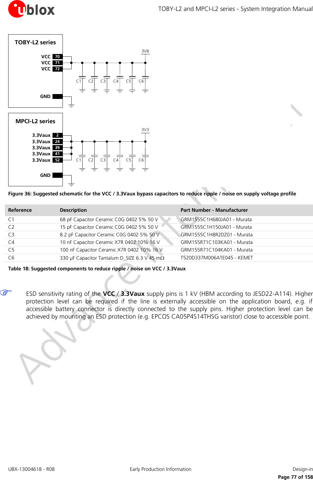
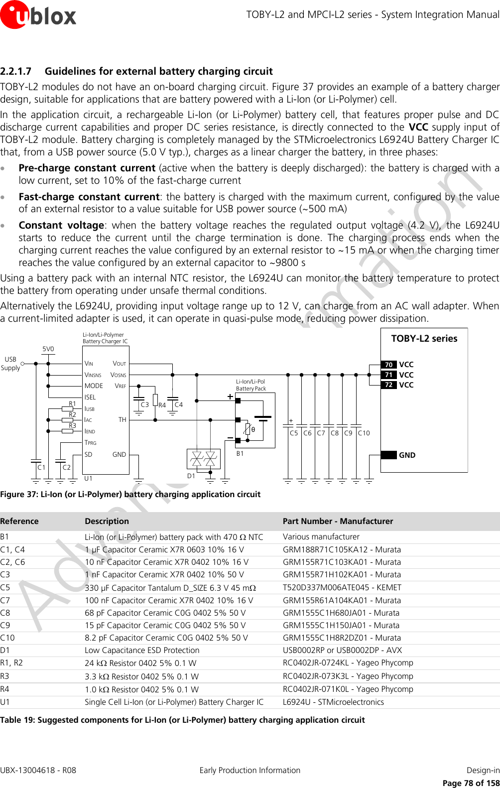
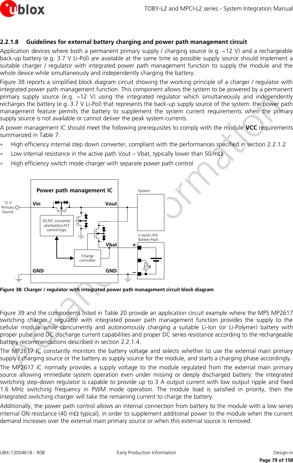
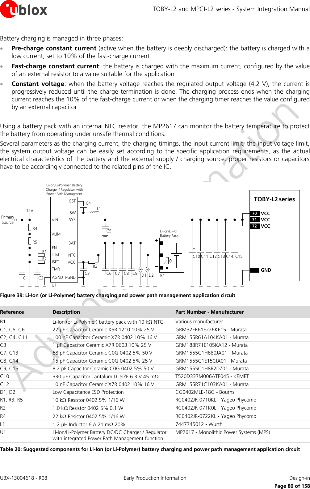
![TOBY-L2 and MPCI-L2 series - System Integration Manual UBX-13004618 - R08 Early Production Information Design-in Page 82 of 158 2.2.2 RTC supply output (V_BCKP) The RTC supply V_BCKP pin is not available on MPCI-L2 series modules. 2.2.2.1 Guidelines for V_BCKP circuit design TOBY-L2 series modules provide the V_BCKP RTC supply input/output, which can be mainly used to: Provide RTC back-up when VCC supply is removed If RTC timing is required to run for a time interval of T [s] when VCC supply is removed, place a capacitor with a nominal capacitance of C [µF] at the V_BCKP pin. Choose the capacitor using the following formula: C [µF] = (Current_Consumption [µA] x T [s]) / Voltage_Drop [V] = 1.25 x T [s] For example, a 100 µF capacitor can be placed at V_BCKP to provide RTC backup holding the V_BCKP voltage within its valid range for around 80 s at 25 °C, after the VCC supply is removed. If a longer buffering time is required, a 70 mF super-capacitor can be placed at V_BCKP, with a 4.7 k series resistor to hold the V_BCKP voltage within its valid range for approximately 15 hours at 25 °C, after the VCC supply is removed. The purpose of the series resistor is to limit the capacitor charging current due to the large capacitor specifications, and also to let a fast rise time of the voltage value at the V_BCKP pin after VCC supply has been provided. These capacitors allow the time reference to run during battery disconnection. TOBY-L2 seriesC1(a)3V_BCKPR2TOBY-L2 seriesC2(superCap)(b)3V_BCKPD3TOBY-L2 seriesB3(c)3V_BCKP Figure 40: Real time clock supply (V_BCKP) application circuits: (a) using a 100 µF capacitor to let the RTC run for ~80 s after VCC removal; (b) using a 70 mF capacitor to let RTC run for ~15 hours after VCC removal; (c) using a non-rechargeable battery Reference Description Part Number - Manufacturer C1 100 µF Tantalum Capacitor GRM43SR60J107M - Murata R2 4.7 kΩ Resistor 0402 5% 0.1 W RC0402JR-074K7L - Yageo Phycomp C2 70 mF Capacitor XH414H-IV01E - Seiko Instruments Table 21: Example of components for V_BCKP buffering If very long buffering time is required to allow the RTC time reference to run during a disconnection of the VCC supply, then an external battery can be connected to V_BCKP pin. The battery should be able to provide a proper nominal voltage and must never exceed the maximum operating voltage for V_BCKP (specified in the Input characteristics of Supply/Power pins table in TOBY-L2 series Data Sheet [1]). The connection of the battery to V_BCKP should be done with a suitable series resistor for a rechargeable battery, or with an appropriate series diode for a non-rechargeable battery. The purpose of the series resistor is to limit the battery charging current due to the battery specifications, and also to allow a fast rise time of the voltage value at the V_BCKP pin after the VCC supply has been provided. The purpose of the series diode is to avoid a current flow from the module V_BCKP pin to the non-rechargeable battery.](https://usermanual.wiki/u-blox/TOBYL280.System-Integrators-Manual/User-Guide-2664029-Page-82.png)
![TOBY-L2 and MPCI-L2 series - System Integration Manual UBX-13004618 - R08 Early Production Information Design-in Page 83 of 158 If the RTC timing is not required when the VCC supply is removed, it is not needed to connect the V_BCKP pin to an external capacitor or battery. In this case the date and time are not updated when VCC is disconnected. If VCC is always supplied, then the internal regulator is supplied from the main supply and there is no need for an external component on V_BCKP. Combining a cellular module with a u-blox GNSS positioning receiver, the positioning receiver VCC supply is controlled by the cellular module by means of the “GNSS supply enable” function provided by the GPIO2 of the cellular module. In this case the V_BCKP supply output of the cellular module can be connected to the V_BCKP backup supply input pin of the GNSS receiver to provide the supply for the positioning real time clock and backup RAM when the VCC supply of the cellular module is within its operating range and the VCC supply of the GNSS receiver is disabled. This enables the u-blox GNSS receiver to recover from a power breakdown with either a hot start or a warm start (depending on the duration of the positioning VCC outage) and to maintain the configuration settings saved in the backup RAM. See section 2.6.3 for more details regarding the application circuit with a u-blox GNSS receiver. V_BCKP supply output pin provides internal short circuit protection to limit start-up current and protect the device in short circuit situations. No additional external short circuit protection is required. Do not apply loads which might exceed the limit for maximum available current from V_BCKP supply (see TOBY-L2 series Data Sheet [1]) as this can cause malfunctions in internal circuitry. ESD sensitivity rating of the V_BCKP supply pin is 1 kV (Human Body Model according to JESD22-A114). Higher protection level could be required if the line is externally accessible and it can be achieved by mounting an ESD protection (e.g. EPCOS CA05P4S14THSG varistor array) close to the accessible point. 2.2.2.2 Guidelines for V_BCKP layout design V_BCKP supply requires careful layout: avoid injecting noise on this voltage domain as it may affect the stability of the internal circuitry.](https://usermanual.wiki/u-blox/TOBYL280.System-Integrators-Manual/User-Guide-2664029-Page-83.png)
![TOBY-L2 and MPCI-L2 series - System Integration Manual UBX-13004618 - R08 Early Production Information Design-in Page 84 of 158 2.2.3 Generic digital interfaces supply output (V_INT) The generic digital interfaces supply V_INT pin is not available on MPCI-L2 series modules. 2.2.3.1 Guidelines for V_INT circuit design TOBY-L2 series provide the V_INT generic digital interfaces 1.8 V supply output, which can be mainly used to: Indicate when the module is switched on (as described in sections 1.6.1, 1.6.2) Pull-up SIM detection signal (see section 2.5 for more details) Supply voltage translators to connect 1.8 V module generic digital interfaces to 3.0 V devices (e.g. see 2.6.2) Pull-up DDC (I2C) interface signals (see section 2.6.3 for more details) Supply a 1.8 V u-blox 6 or subsequent u-blox GNSS receiver generation (see section 2.6.3 for more details) V_INT supply output pin provides internal short circuit protection to limit start-up current and protect the device in short circuit situations. No additional external short circuit protection is required. Do not apply loads which might exceed the limit for maximum available current from V_INT supply (see the TOBY-L2 series Data Sheet [1]) as this can cause malfunctions in internal circuitry. Since the V_INT supply is generated by an internal switching step-down regulator, the V_INT voltage ripple can range as specified in the TOBY-L2 series Data Sheet [1]: it is not recommended to supply sensitive analog circuitry without adequate filtering for digital noise. V_INT can only be used as an output: do not connect any external supply source on V_INT. ESD sensitivity rating of the V_INT supply pin is 1 kV (Human Body Model according to JESD22-A114). Higher protection level could be required if the line is externally accessible and it can be achieved by mounting an ESD protection (e.g. EPCOS CA05P4S14THSG varistor array) close to the accessible point. It is recommended to provide direct access to the V_INT pin on the application board by means of an accessible test point directly connected to the V_INT pin. 2.2.3.2 Guidelines for V_INT layout design V_INT supply output is generated by an integrated switching step-down converter. Because of this, it can be a source of noise: avoid coupling with sensitive signals.](https://usermanual.wiki/u-blox/TOBYL280.System-Integrators-Manual/User-Guide-2664029-Page-84.png)
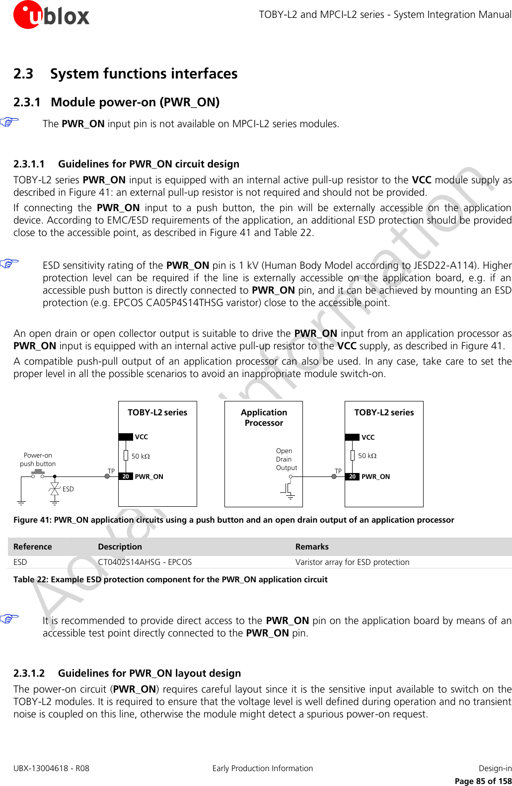
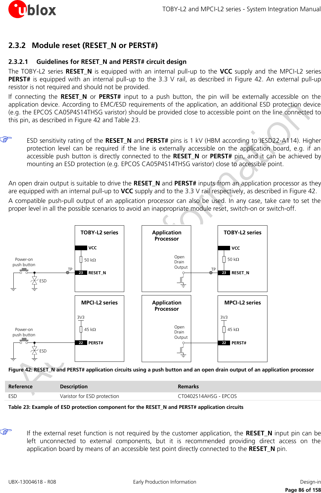
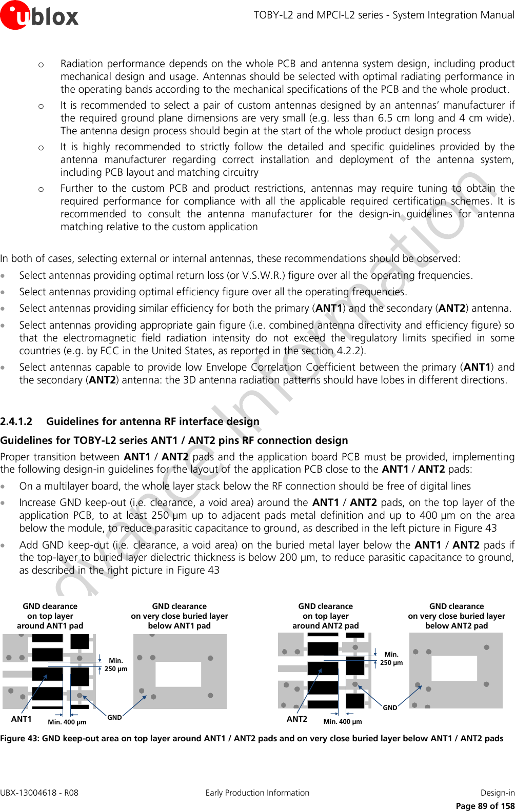
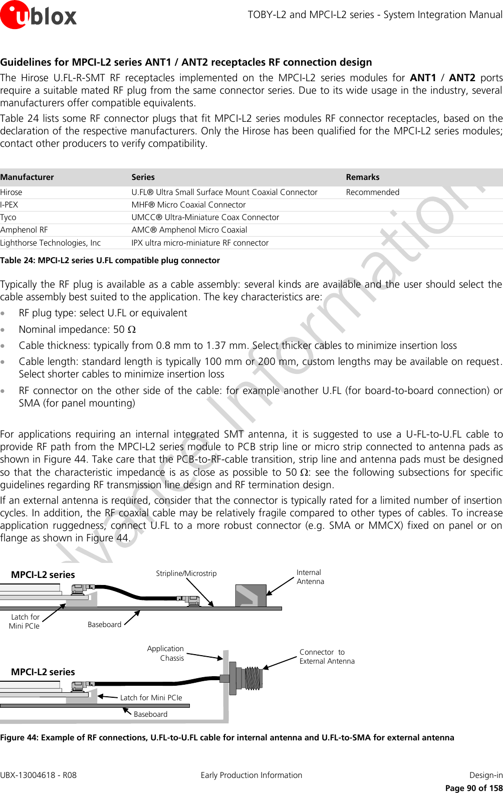
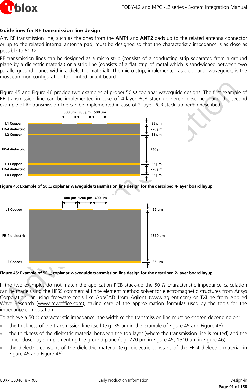
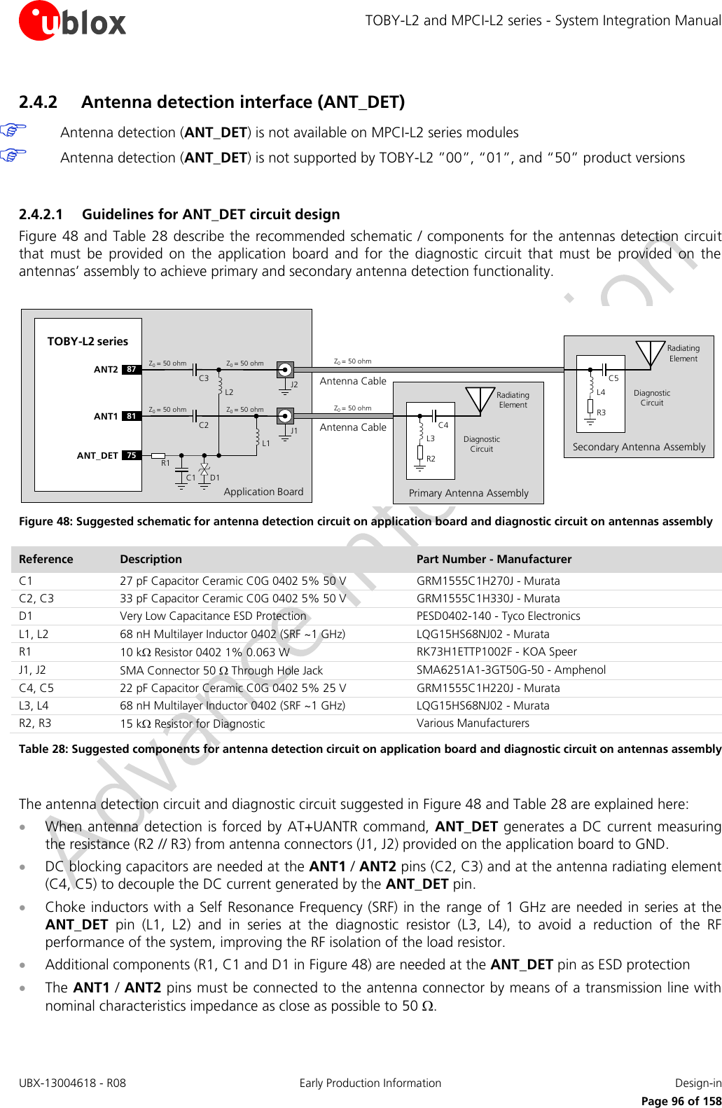
![TOBY-L2 and MPCI-L2 series - System Integration Manual UBX-13004618 - R08 Early Production Information Design-in Page 97 of 158 The DC impedance at RF port for some antennas may be a DC open (e.g. linear monopole) or a DC short to reference GND (e.g. PIFA antenna). For those antennas, without the diagnostic circuit of Figure 48, the measured DC resistance is always at the limits of the measurement range (respectively open or short), and there is no means to distinguish between a defect on antenna path with similar characteristics (respectively: removal of linear antenna or RF cable shorted to GND for PIFA antenna). Furthermore, any other DC signal injected to the RF connection from ANT connector to radiating element will alter the measurement and produce invalid results for antenna detection. It is recommended to use an antenna with a built-in diagnostic resistor in the range from 5 k to 30 k to assure good antenna detection functionality and avoid a reduction of module RF performance. The choke inductor should exhibit a parallel Self Resonance Frequency (SRF) in the range of 1 GHz to improve the RF isolation of load resistor. For example: Consider an antenna with built-in DC load resistor of 15 k. Using the +UANTR AT command, the module reports the resistance value evaluated from the antenna connector provided on the application board to GND: Reported values close to the used diagnostic resistor nominal value (i.e. values from 13 k to 17 k if a 15 k diagnostic resistor is used) indicate that the antenna is properly connected. Values close to the measurement range maximum limit (approximately 50 k) or an open-circuit “over range” report (see u-blox AT Commands Manual [3]) means that that the antenna is not connected or the RF cable is broken. Reported values below the measurement range minimum limit (1 k) highlights a short to GND at antenna or along the RF cable. Measurement inside the valid measurement range and outside the expected range may indicate an improper connection, damaged antenna or wrong value of antenna load resistor for diagnostic. Reported value could differ from the real resistance value of the diagnostic resistor mounted inside the antenna assembly due to antenna cable length, antenna cable capacity and the used measurement method. If the primary / secondary antenna detection function is not required by the customer application, the ANT_DET pin can be left not connected and the ANT1 / ANT2 pins can be directly connected to the related antenna connector by means of a 50 transmission line as described in Figure 47. 2.4.2.1 Guidelines for ANT_DET layout design The recommended layout for the primary antenna detection circuit to be provided on the application board to achieve the primary antenna detection functionality, implementing the recommended schematic described in Figure 48 and Table 28, is explained here: The ANT1 / ANT2 pins have to be connected to the antenna connector by means of a 50 transmission line, implementing the design guidelines described in section 2.4.1 and the recommendations of the SMA connector manufacturer. DC blocking capacitor at ANT1 / ANT2 pins (C2, C3) has to be placed in series to the 50 RF line. The ANT_DET pin has to be connected to the 50 transmission line by means of a sense line. Choke inductors in series at the ANT_DET pin (L1, L2) have to be placed so that one pad is on the 50 transmission line and the other pad represents the start of the sense line to the ANT_DET pin. The additional components (R1, C1 and D1) on the ANT_DET line have to be placed as ESD protection.](https://usermanual.wiki/u-blox/TOBYL280.System-Integrators-Manual/User-Guide-2664029-Page-97.png)
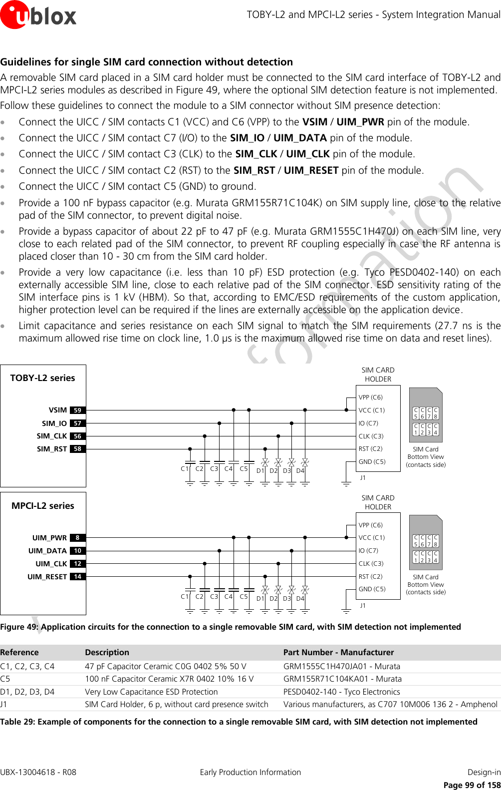
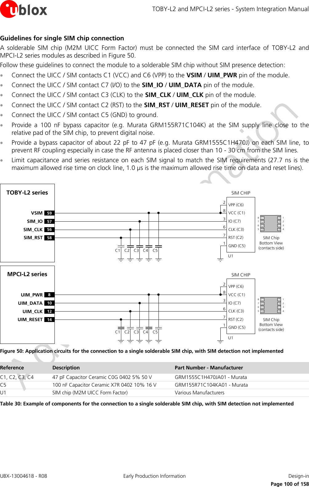
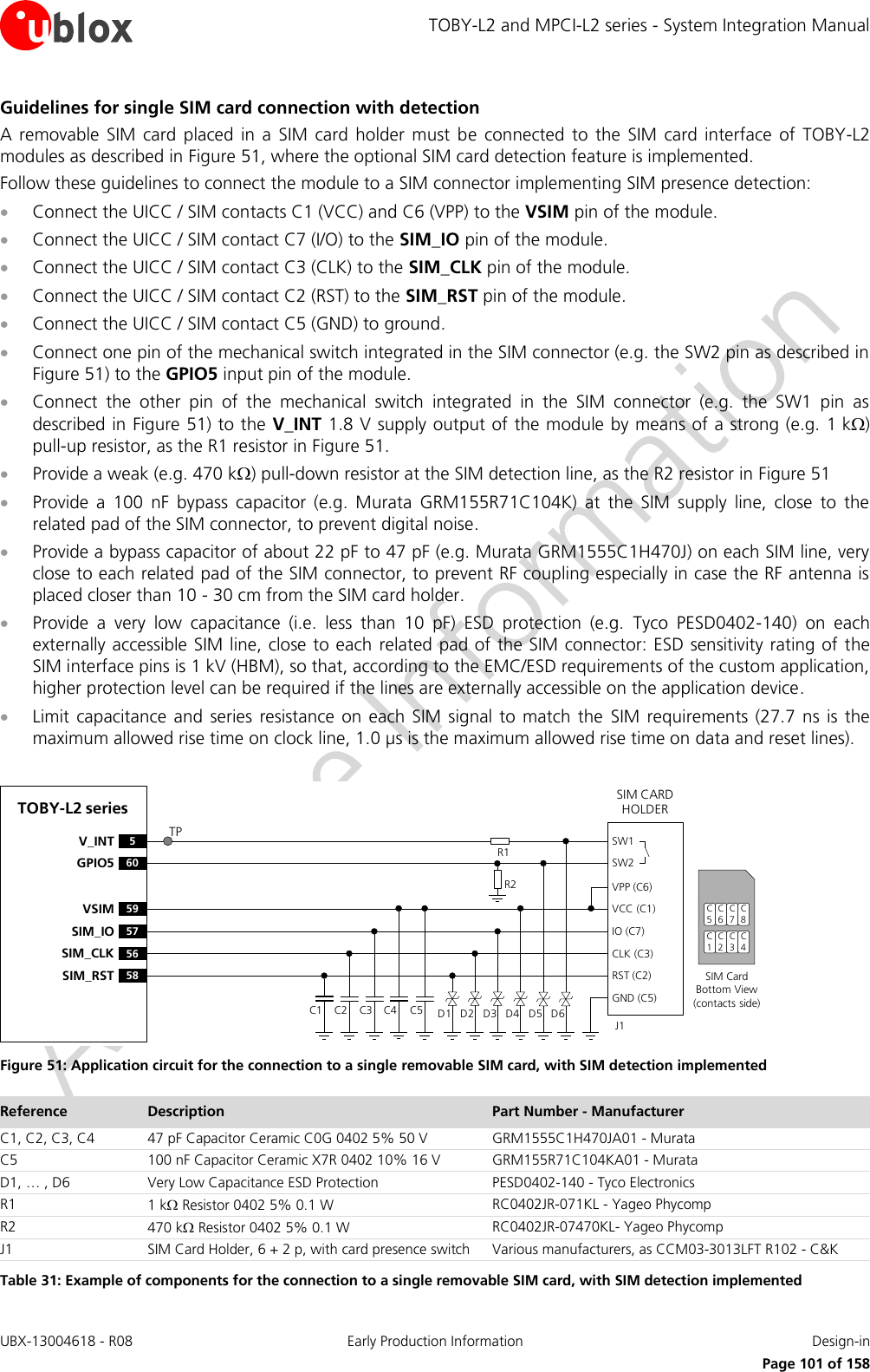
![TOBY-L2 and MPCI-L2 series - System Integration Manual UBX-13004618 - R08 Early Production Information Design-in Page 102 of 158 Guidelines for dual SIM card / chip connection Two SIM card / chip can be connected to the SIM interface of TOBY-L2 and MPCI-L2 series modules as described in the application circuits of Figure 52. TOBY-L2 and MPCI-L2 series modules do not support the usage of two SIM at the same time, but two SIM can be populated on the application board, providing a proper switch to connect only the first or only the second SIM at a time to the SIM interface of the modules, as described in Figure 52. TOBY-L2 “00”, “01”, and “50” product versions and MPCI-L2 modules do not support SIM hot insertion / removal functionality: the physical connection between the external SIM and the module has to be provided before the module boot and then held for normal operation. Switching from one SIM to another can only be properly done within one of these two time periods: after module switch-off by the AT+CPWROFF and before module switch-on by PWR_ON after network deregistration by AT+COPS=2 and before module reset by AT+CFUN=16 TOBY-L2 modules (except “00”, “01”, “50” product versions) support SIM hot insertion / removal on the GPIO5 pin: if the feature is enabled using the specific AT commands (see sections 1.8.2 and 1.11, and u-blox AT Commands Manual [3], +UGPIOC, +UDCONF commands), the switch from first SIM to the second SIM can be properly done when a Low logic level is present on the GPIO5 pin (“SIM not inserted” = SIM interface not enabled), without the necessity of a module re-boot, so that the SIM interface will be re-enabled by the module to use the second SIM when a high logic level is re-applied on the GPIO5 pin. In the application circuit example represented in Figure 52, the application processor will drive the SIM switch using its own GPIO to properly select the SIM that is used by the module. Another GPIO may be used to handle the SIM hot insertion / removal function of TOBY-L2 modules, which can also be handled by other external circuits or by the cellular module GPIO according to the application requirements. The dual SIM connection circuit described in Figure 52 can be implemented for SIM chips as well, providing proper connection between SIM switch and SIM chip as described in Figure 50. If it is required to switch between more than 2 SIM, a circuit similar to the one described in Figure 52 can be implemented: in case of 4 SIM circuit, using proper 4-throw switch instead of the suggested 2-throw switches. Follow these guidelines to connect the module to two external SIM connectors: Use a proper low on resistance (i.e. few ohms) and low on capacitance (i.e. few pF) 2-throw analog switch (e.g. Fairchild FSA2567) as SIM switch to ensure high-speed data transfer according to SIM requirements. Connect the contacts C1 (VCC) and C6 (VPP) of the two UICC / SIM to the VSIM / UIM_PWR pin of the module by means of a proper 2-throw analog switch (e.g. Fairchild FSA2567). Connect the contact C7 (I/O) of the two UICC / SIM to the SIM_IO / UIM_DATA pin of the module by means of a proper 2-throw analog switch (e.g. Fairchild FSA2567). Connect the contact C3 (CLK) of the two UICC / SIM to the SIM_CLK / UIM_CLK pin of the module by means of a proper 2-throw analog switch (e.g. Fairchild FSA2567). Connect the contact C2 (RST) of the two UICC / SIM to the SIM_RST / UIM_RESET pin of the module by means of a proper 2-throw analog switch (e.g. Fairchild FSA2567). Connect the contact C5 (GND) of the two UICC / SIM to ground. Provide a 100 nF bypass capacitor (e.g. Murata GRM155R71C104K) at the SIM supply (VSIM / UIM_PWR), close to the related pad of the two SIM connectors, to prevent digital noise. Provide a bypass capacitor of about 22 pF to 47 pF (e.g. Murata GRM1555C1H470J) on each SIM line, very close to each related pad of the two SIM connectors, to prevent RF coupling especially in case the RF antenna is placed closer than 10 - 30 cm from the SIM card holders. Provide a very low capacitance (i.e. less than 10 pF) ESD protection (e.g. Tyco Electronics PESD0402-140) on each externally accessible SIM line, close to each pad of the two SIM connectors, according to the EMC/ESD requirements of the custom application. Limit capacitance and series resistance on each SIM signal to match the SIM requirements (27.7 ns is the maximum allowed rise time on clock line, 1.0 µs is the maximum allowed rise time on data and reset lines).](https://usermanual.wiki/u-blox/TOBYL280.System-Integrators-Manual/User-Guide-2664029-Page-102.png)
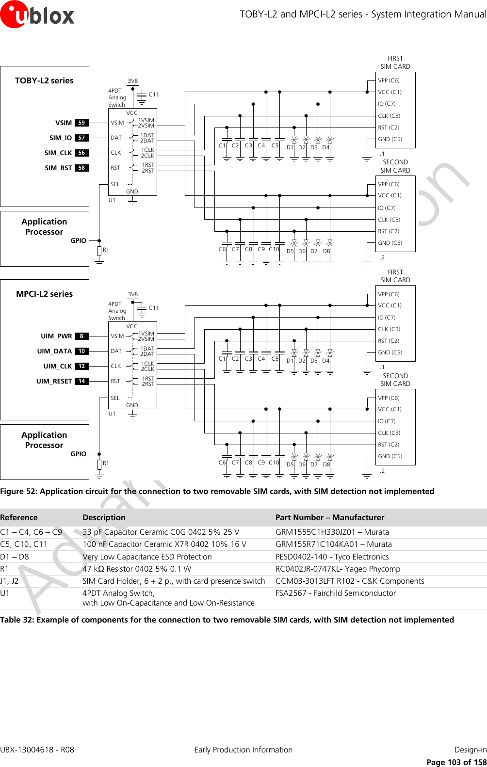
![TOBY-L2 and MPCI-L2 series - System Integration Manual UBX-13004618 - R08 Early Production Information Design-in Page 105 of 158 2.6 Data communication interfaces 2.6.1 Universal Serial Bus (USB) 2.6.1.1 Guidelines for USB circuit design The USB_D+ and USB_D- lines carry the USB serial data and signaling. The lines are used in single ended mode for full speed signaling handshake, as well as in differential mode for high speed signaling and data transfer. USB pull-up or pull-down resistors and external series resistors on USB_D+ and USB_D- lines as required by the USB 2.0 specification [6] are part of the module USB pin driver and do not need to be externally provided. The additional VUSB_DET input is available as optional feature to sense the host VBUS voltage (5.0 V typical). The VUSB_DET functionality is not supported by TOBY-L2 “00”, “01”, and “50” product versions: the pin should be left unconnected or it should not be driven high (for more details, see section 1.9.1.1). The VUSB_DET pin is not available on MPCI-L2 series modules. Routing the USB pins to a connector, they will be externally accessible on the application device. According to EMC/ESD requirements of the application, an additional ESD protection device with very low capacitance should be provided close to accessible point on the line connected to this pin, as described in Figure 53 and Table 33. The USB interface pins ESD sensitivity rating is 1 kV (Human Body Model according to JESD22-A114F). Higher protection level could be required if the lines are externally accessible and it can be achieved by mounting a very low capacitance (i.e. less or equal to 1 pF) ESD protection (e.g. Tyco Electronics PESD0402-140 ESD protection device) on the lines connected to these pins, close to accessible points. The USB_D+ and USB_D- pins of the modules can be directly connected to the USB host application processor without additional ESD protections if they are not externally accessible or according to EMC/ESD requirements. D+D-GND28 USB_D+27 USB_D-GNDUSB DEVICE CONNECTORVBUSD+D-GND28 USB_D+27 USB_D-GNDUSB HOST PROCESSORD+D-GND38 USB_D+36 USB_D-GNDUSB DEVICE CONNECTORVBUSTOBY-L2 series TOBY-L2 series MPCI-L2 series MPCI-L2 series D+D-GND38 USB_D+36 USB_D-GNDUSB HOST PROCESSORVBUS 4VUSB_DET4VUSB_DETD1 D2D1 D2VBUS Figure 53: USB Interface application circuits Reference Description Part Number - Manufacturer D1, D2 Very Low Capacitance ESD Protection PESD0402-140 - Tyco Electronics Table 33: Component for USB application circuits](https://usermanual.wiki/u-blox/TOBYL280.System-Integrators-Manual/User-Guide-2664029-Page-105.png)
![TOBY-L2 and MPCI-L2 series - System Integration Manual UBX-13004618 - R08 Early Production Information Design-in Page 106 of 158 If the USB interface pins are not used, they can be left unconnected on the application board, but it is recommended providing accessible test points directly connected to USB_D+ and USB_D- pins. 2.6.1.2 Guidelines for USB layout design The USB_D+ / USB_D- lines require accurate layout design to achieve reliable signaling at the high speed data rate (up to 480 Mb/s) supported by the USB serial interface. The characteristic impedance of the USB_D+ / USB_D- lines is specified by the Universal Serial Bus Revision 2.0 specification [6]. The most important parameter is the differential characteristic impedance applicable for the odd-mode electromagnetic field, which should be as close as possible to 90 differential. Signal integrity may be degraded if PCB layout is not optimal, especially when the USB signaling lines are very long. Use the following general routing guidelines to minimize signal quality problems: Route USB_D+ / USB_D- lines as a differential pair Route USB_D+ / USB_D- lines as short as possible Ensure the differential characteristic impedance (Z0) is as close as possible to 90 Ensure the common mode characteristic impedance (ZCM) is as close as possible to 30 Consider design rules for USB_D+ / USB_D- similar to RF transmission lines, being them coupled differential micro-strip or buried stripline: avoid any stubs, abrupt change of layout, and route on clear PCB area Figure 54 and Figure 55 provide two examples of coplanar waveguide designs with differential characteristic impedance close to 90 and common mode characteristic impedance close to 30 . The first transmission line can be implemented in case of 4-layer PCB stack-up herein described, the second transmission line can be implemented in case of 2-layer PCB stack-up herein described. 35 µm35 µm35 µm35 µm270 µm270 µm760 µmL1 CopperL3 CopperL2 CopperL4 CopperFR-4 dielectricFR-4 dielectricFR-4 dielectric350 µm 400 µm400 µm350 µm400 µm Figure 54: Example of USB line design, with Z0 close to 90 and ZCM close to 30 , for the described 4-layer board layup 35 µm35 µm1510 µmL2 CopperL1 CopperFR-4 dielectric740 µm 410 µm410 µm740 µm410 µm Figure 55: Example of USB line design, with Z0 close to 90 and ZCM close to 30 , for the described 2-layer board layup](https://usermanual.wiki/u-blox/TOBYL280.System-Integrators-Manual/User-Guide-2664029-Page-106.png)
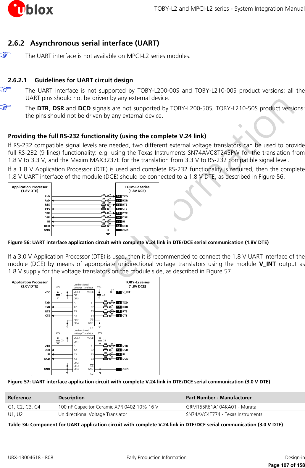
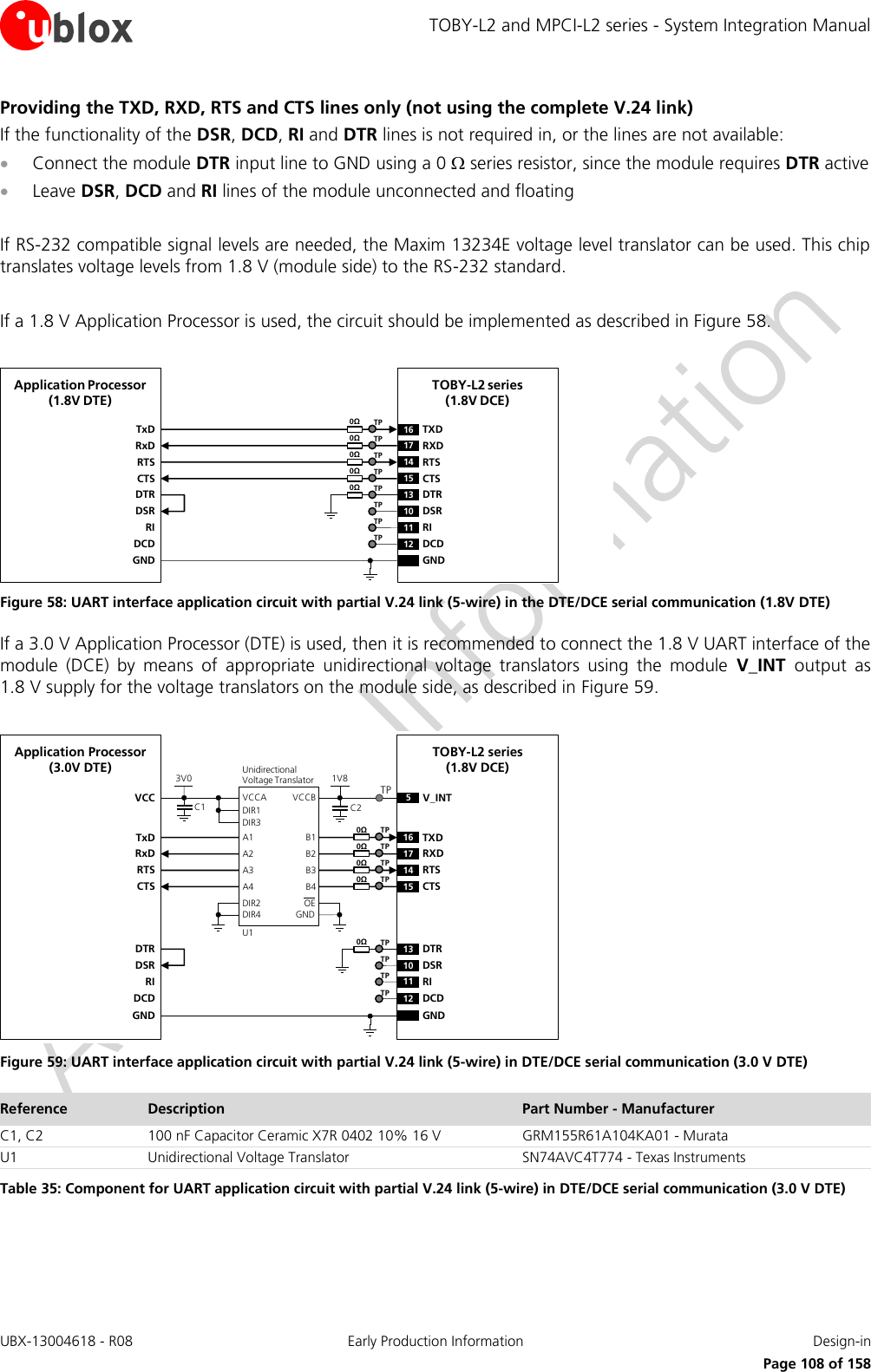
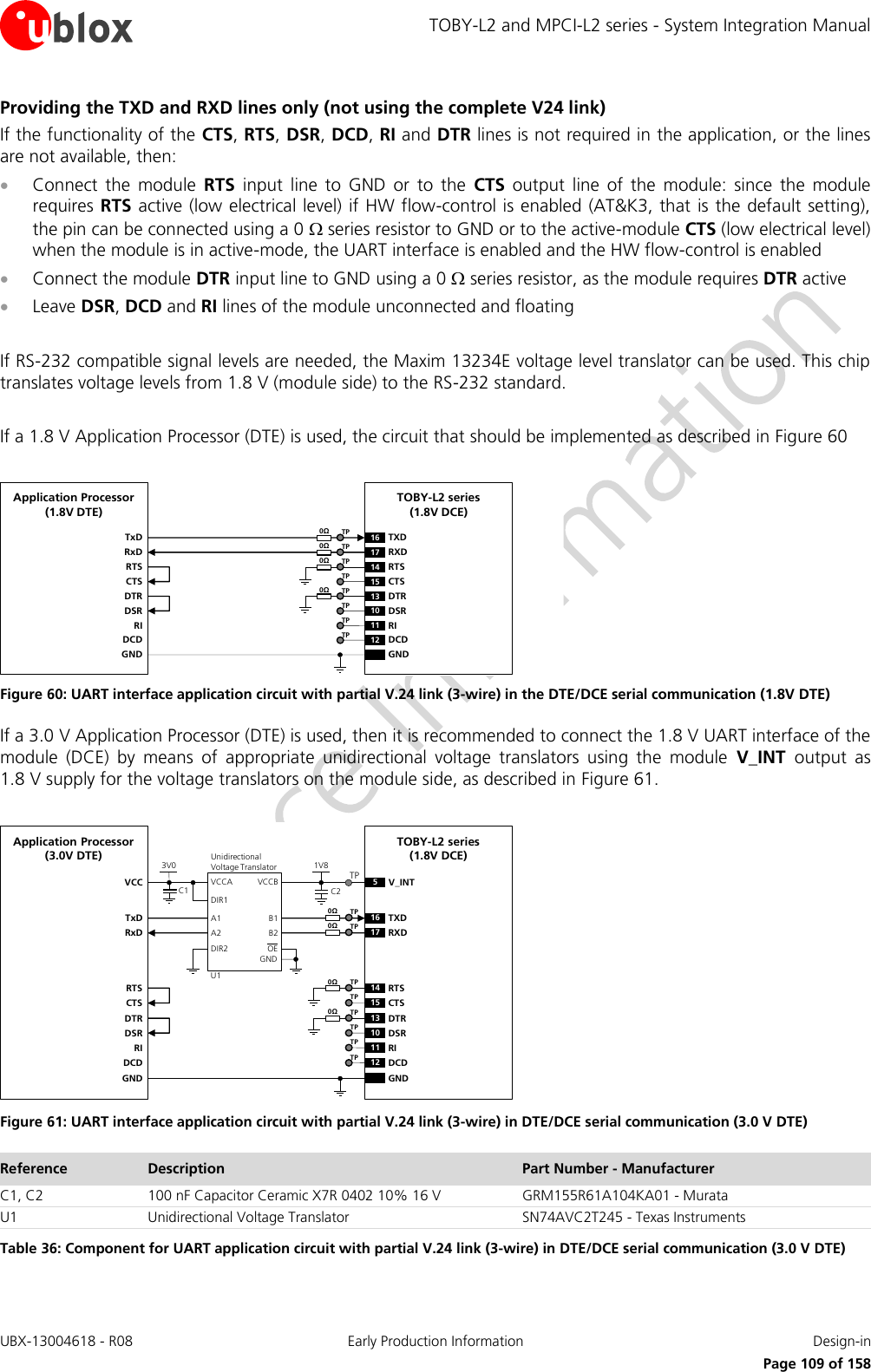
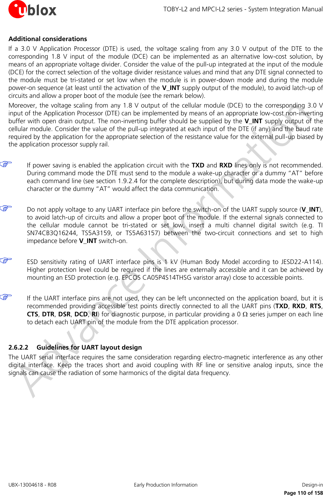
![TOBY-L2 and MPCI-L2 series - System Integration Manual UBX-13004618 - R08 Early Production Information Design-in Page 111 of 158 2.6.3 DDC (I2C) interface The I2C bus compatible Display Data Channel interface is not available on MPCI-L2 series modules. 2.6.3.1 Guidelines for DDC (I2C) circuit design I2C bus function is not supported by TOBY-L2 “00”, “01”, and “50” product versions: the pins should not be driven by any external device. General considerations The DDC I2C-bus master interface can be used to communicate with u-blox GNSS receivers and other external I2C-bus slaves as an audio codec. Beside the general considerations reported below, see: the following parts of this section for specific guidelines for the connection to u-blox GNSS receivers the section 2.7.1 for an application circuit example with an external audio codec I2C-bus slave To be compliant with the I2C bus specifications, the module bus interface pads are open drain output and pull up resistors must be mounted externally. Resistor values must conform to I2C bus specifications [12]: for example, 4.7 k resistors can be commonly used. Pull-ups must be connected to a supply voltage of 1.8 V (typical), since this is the voltage domain of the DDC pins which are not tolerant to higher voltage values (e.g. 3.0 V). Connect the DDC (I2C) pull-ups to the V_INT 1.8 V supply source, or another 1.8 V supply source enabled after V_INT (e.g., as the GNSS 1.8 V supply present in Figure 62 application circuit), as any external signal connected to the DDC (I2C) interface must not be set high before the switch-on of the V_INT supply of DDC pins, to avoid latch-up of circuits and let a proper boot of the module. The signal shape is defined by the values of the pull-up resistors and the bus capacitance. Long wires on the bus will increase the capacitance. If the bus capacitance is increased, use pull-up resistors with nominal resistance value lower than 4.7 k, to match the I2C bus specifications [12] regarding rise and fall times of the signals. Capacitance and series resistance must be limited on the bus to match the I2C specifications (1.0 µs is the maximum allowed rise time on the SCL and SDA lines): route connections as short as possible. If the pins are not used as DDC bus interface, they can be left unconnected. ESD sensitivity rating of the DDC (I2C) pins is 1 kV (Human Body Model according to JESD22-A114). Higher protection level could be required if the lines are externally accessible and it can be achieved by mounting an ESD protection (e.g. EPCOS CA05P4S14THSG varistor array) close to accessible points.](https://usermanual.wiki/u-blox/TOBYL280.System-Integrators-Manual/User-Guide-2664029-Page-111.png)
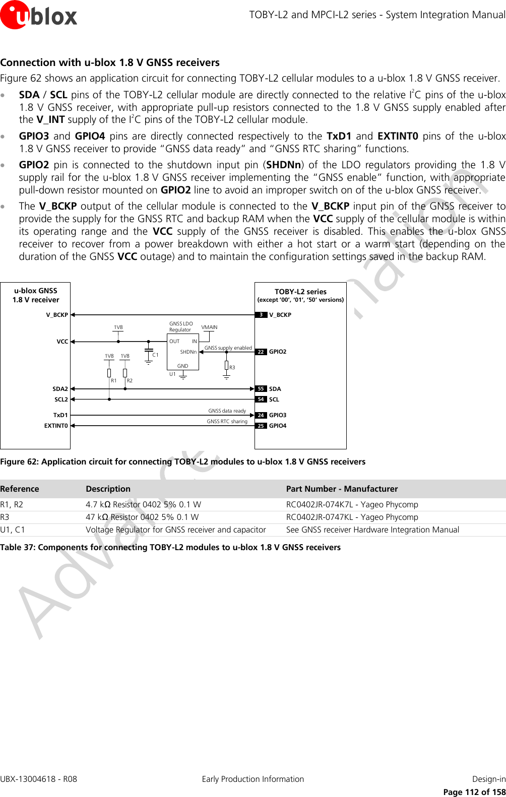
![TOBY-L2 and MPCI-L2 series - System Integration Manual UBX-13004618 - R08 Early Production Information Design-in Page 113 of 158 Figure 63 illustrates an alternative application circuit solution in which the TOBY-L2 supplies a u-blox 1.8 V GNSS receiver. The V_INT 1.8 V regulated supply output of a TOBY-L2 module can be used as supply source for a u-blox 1.8 V GNSS receiver (u-blox 6 generation receiver or newer) instead of using an external voltage regulator, as shown in Figure 62. The V_INT supply is able to support the maximum current consumption of these positioning receivers. The internal switching step-down regulator that generates the V_INT supply is set to 1.8 V (typical) when the cellular module is switched on and it is disabled when the module is switched off. The supply of the u-blox 1.8 V GNSS receiver can be switched off using an external p-channel MOS controlled by the GPIO2 pin of TOBY-L2 cellular modules by means of a proper inverting transistor as shown in Figure 63, implementing the “GNSS supply enable” function. If this feature is not required, the V_INT supply output can be directly connected to the u-blox 1.8 V GNSS receiver, so that it will switch on when V_INT output is enabled. According to the V_INT supply output voltage ripple characteristic specified in the TOBY-L2 Data Sheet [1]: Additional filtering may be needed to properly supply an external LNA, depending on the characteristics of the used LNA, adding a series ferrite bead and a bypass capacitor (e.g. the Murata BLM15HD182SN1 ferrite bead and the Murata GRM1555C1H220J 22 pF capacitor) at the input of the external LNA supply line u-blox GNSS1.8 V receiverTxD1EXTINT0V_BCKP V_BCKP3SDA2SCL2VCC1V8C1R35V_INTR5R4TPT2T1R1 R21V8 1V8GNSS data readyGNSS RTC sharingGNSS supply enabled 22 GPIO2SDASCLGPIO3GPIO455542425TOBY-L2 series(except ‘00’, ‘01’, ‘50’ versions) Figure 63: Application circuit for connecting TOBY-L2 modules to u-blox 1.8 V GNSS receivers using V_INT as supply Reference Description Part Number - Manufacturer R1, R2 4.7 k Resistor 0402 5% 0.1 W RC0402JR-074K7L - Yageo Phycomp R3 47 k Resistor 0402 5% 0.1 W RC0402JR-0747KL - Yageo Phycomp R4 10 k Resistor 0402 5% 0.1 W RC0402JR-0710KL - Yageo Phycomp R5 100 k Resistor 0402 5% 0.1 W RC0402JR-07100KL - Yageo Phycomp T1 P-Channel MOSFET Low On-Resistance IRLML6401 - International Rectifier or NTZS3151P - ON Semi T2 NPN BJT Transistor BC847 - Infineon C1 100 nF Capacitor Ceramic X7R 0402 10% 16 V GRM155R71C104KA01 - Murata Table 38: Components for connecting TOBY-L2 modules to u-blox 1.8 V GNSS receivers using V_INT as supply For additional guidelines regarding the design of applications with u-blox 1.8 V GNSS receivers see the GNSS Implementation Application Note [13] and the Hardware Integration Manual of the u-blox GNSS receivers.](https://usermanual.wiki/u-blox/TOBYL280.System-Integrators-Manual/User-Guide-2664029-Page-113.png)
![TOBY-L2 and MPCI-L2 series - System Integration Manual UBX-13004618 - R08 Early Production Information Design-in Page 114 of 158 Connection with u-blox 3.0 V GNSS receivers Figure 64 shows an application circuit for connecting TOBY-L2 cellular modules to a u-blox 3.0 V GNSS receiver: As the SDA and SCL pins of the TOBY-L2 cellular module are not tolerant up to 3.0 V, the connection to the related I2C pins of the u-blox 3.0 V GNSS receiver must be provided using a proper I2C-bus Bidirectional Voltage Translator with proper pull-up resistors (e.g. the TI TCA9406 additionally provides the partial power down feature so that the GNSS 3.0 V supply can be ramped up before the V_INT 1.8 V cellular supply). As the GPIO3 and GPIO4 pins of the TOBY-L2 cellular module are not tolerant up to 3.0 V, the connection to the related pins of the u-blox 3.0 V GNSS receiver must be provided using a proper Unidirectional General Purpose Voltage Translator (e.g. TI SN74AVC2T245, which additionally provides the partial power down feature so that the 3.0 V GNSS supply can be also ramped up before the V_INT 1.8 V cellular supply). GPIO2 pin is connected to the shutdown input pin (SHDNn) of the LDO regulators providing the 3.0 V supply rail for the u-blox 3.0 V GNSS receiver implementing the “GNSS enable” function, with appropriate pull-down resistor mounted on GPIO2 line to avoid an improper switch on of the u-blox GNSS receiver. The V_BCKP supply output of the cellular module can be directly connected to the V_BCKP backup supply input pin of the GNSS receiver as in the application circuit for a u-blox 1.8 V GNSS receiver. u-blox GNSS 3.0 V receiver24 GPIO325 GPIO41V8B1 A1GNDU3B2A2VCCBVCCAUnidirectionalVoltage TranslatorC4 C53V0TxD1EXTINT0R1INOUTGNSS LDO RegulatorSHDNnR2VMAIN3V0U122 GPIO255 SDA54 SCLR4 R51V8SDA_A SDA_BGNDU2SCL_ASCL_BVCCAVCCBI2C-bus Bidirectional Voltage Translator2V_INTC1C2 C3R3SDA2SCL2VCCDIR1DIR23V_BCKPV_BCKPOEnOEGNSS data readyGNSS RTC sharingGNSS supply enabledTOBY-L2 series (except ‘00’, ‘01’, ‘50’ versions)GND Figure 64: Application circuit for connecting TOBY-L2 modules to u-blox 3.0 V GNSS receivers Reference Description Part Number - Manufacturer R1, R2, R4, R5 4.7 kΩ Resistor 0402 5% 0.1 W RC0402JR-074K7L - Yageo Phycomp R3 47 kΩ Resistor 0402 5% 0.1 W RC0402JR-0747KL - Yageo Phycomp C2, C3, C4, C5 100 nF Capacitor Ceramic X5R 0402 10% 10V GRM155R71C104KA01 - Murata U1, C1 Voltage Regulator for GNSS receiver and capacitor See GNSS receiver Hardware Integration Manual U2 I2C-bus Bidirectional Voltage Translator TCA9406DCUR - Texas Instruments U3 Generic Unidirectional Voltage Translator SN74AVC2T245 - Texas Instruments Table 39: Components for connecting TOBY-L2 modules to u-blox 3.0 V GNSS receivers For additional guidelines regarding the design of applications with u-blox 3.0 V GNSS receivers see the GNSS Implementation Application Note [13] and the Hardware Integration Manual of the u-blox GNSS receivers. 2.6.3.2 Guidelines for DDC (I2C) layout design The DDC (I2C) serial interface requires the same consideration regarding electro-magnetic interference as any other digital interface. Keep the traces short and avoid coupling with RF line or sensitive analog inputs, since the signals can cause the radiation of some harmonics of the digital data frequency.](https://usermanual.wiki/u-blox/TOBYL280.System-Integrators-Manual/User-Guide-2664029-Page-114.png)
![TOBY-L2 and MPCI-L2 series - System Integration Manual UBX-13004618 - R08 Early Production Information Design-in Page 115 of 158 2.6.4 Secure Digital Input Output interface (SDIO) The SDIO Secure Digital Input Output interface is not available on MPCI-L2 series modules. 2.6.4.1 Guidelines for SDIO circuit design The functionality of the SDIO Secure Digital Input Output interface pins is not supported by TOBY-L2 “00” and “01” product versions: the pins should not be driven by any external device. TOBY-L2 series modules include a 4-bit Secure Digital Input Output interface (SDIO_D0, SDIO_D1, SDIO_D2, SDIO_D3, SDIO_CLK, SDIO_CMD) designed to communicate with an external u-blox short range Wi-Fi module. Combining a u-blox cellular module with a u-blox short range communication module gives designers full access to the Wi-Fi module directly via the cellular module, so that a second interface connected to the Wi-Fi module is not necessary. AT commands via the AT interfaces of the cellular module (UART, USB) allows full control of the Wi-Fi module from any host processor, because Wi-Fi control messages are relayed to the Wi-Fi module via the dedicated SDIO interface (for more details, see the Wi-Fi AT commands in the u-blox AT Commands Manual [3] and see the Wi-Fi / Cellular Integration Application Note [14]). Figure 65 and Table 40 show an application circuit for connecting TOBY-L2 series cellular modules “50” product version to u-blox ELLA-W1 series short range Wi-Fi 802.11 b/g/n modules: The SDIO pins of the cellular module are connected to the related SDIO pins of the u-blox ELLA-W1 series short range Wi-Fi module, with appropriate low value series damping resistors to avoid reflections and other losses in signal integrity, which may create ringing and loss of a square wave shape. The most appropriate value for the series damping resistors on the SDIO lines depends on the specific line lengths and layout implemented. In general, the SDIO series resistors are not strictly required, but it is recommended to slow the SDIO signal, for example with 22 or 33 resistors, and avoid any possible ringing problem without violating the rise / fall time requirements. The V_INT supply output pin of the cellular module is connected to the shutdown input pin (SHDNn) of the two LDO regulators providing the 3.3 V and 1.8 V supply rails for the u-blox ELLA-W1 series Wi-Fi module, with appropriate pull-down resistors to avoid an improper switch on of the Wi-Fi module before the switch-on of the V_INT supply source of the cellular module SDIO interface pins. The GPIO1 pin of the cellular module is connected to the active low full power down input pin (PDn) of the u-blox ELLA-W1 series Wi-Fi module, implementing the Wi-Fi enable function. The configuration pin (CFG) of the u-blox ELLA-W1 series Wi-Fi module is connected to ground by means of a proper pull-down resistor for operation without sleep clock The sleep clock input pin (SLEEP_CLK) of the u-blox ELLA-W1 series Wi-Fi module is left not connected, because an external clock source is not required for full power mode and automotive use. The WLAN LED open drain output pin (LED_0) of the u-blox ELLA-W1 series Wi-Fi module is connected to an LED with appropriate current limiting resistor, indicating Wi-Fi activity as additional optional feature. The WLAN antenna RF input/output (ANT1) of the u-blox ELLA-W1 series Wi-Fi module is connected to a Wi-Fi antenna with an appropriate series Wi-Fi band-pass filter specifically designed for the coexistence between the Wi-Fi RF signals (2402...2482 MHz) and the LTE band 7 RF signals (2500...2690 MHz), as for example the Wi-Fi BAW band-pass filter TDK EPCOS B9604, or the TriQuint 885071, or the TriQuint 885032 or the Avago ACPF-7424, or the Taiyo Yuden F6HF2G441AF46. All GND pins of the cellular module and the u-blox ELLA-W1 series Wi-Fi module are connected to ground. All the other pins of the u-blox ELLA-W1 series Wi-Fi module are intended to be not connected.](https://usermanual.wiki/u-blox/TOBYL280.System-Integrators-Manual/User-Guide-2664029-Page-115.png)
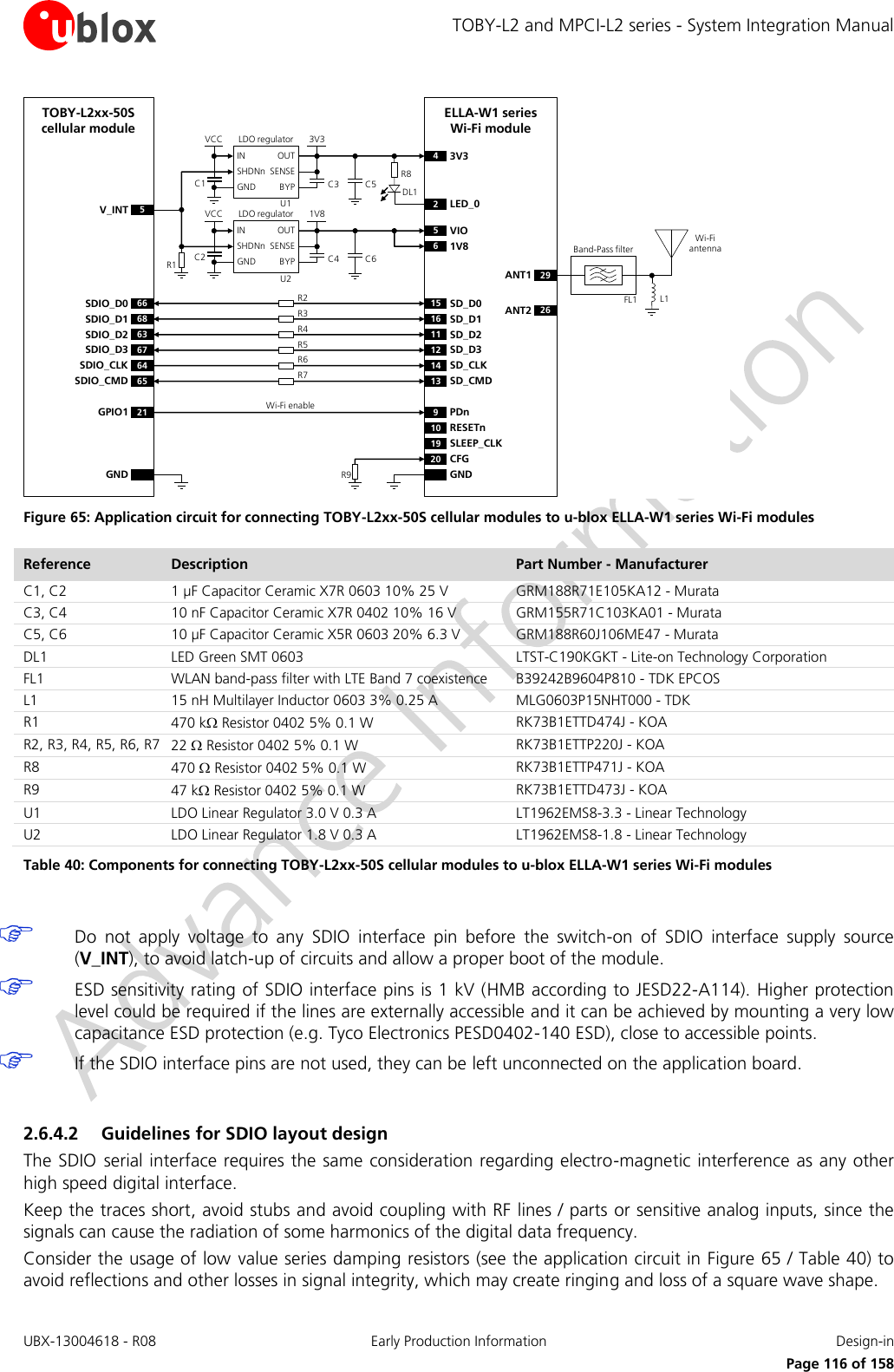
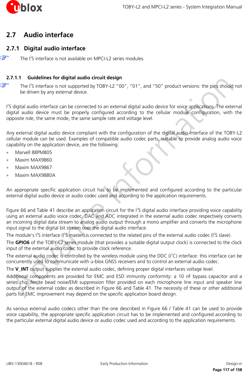
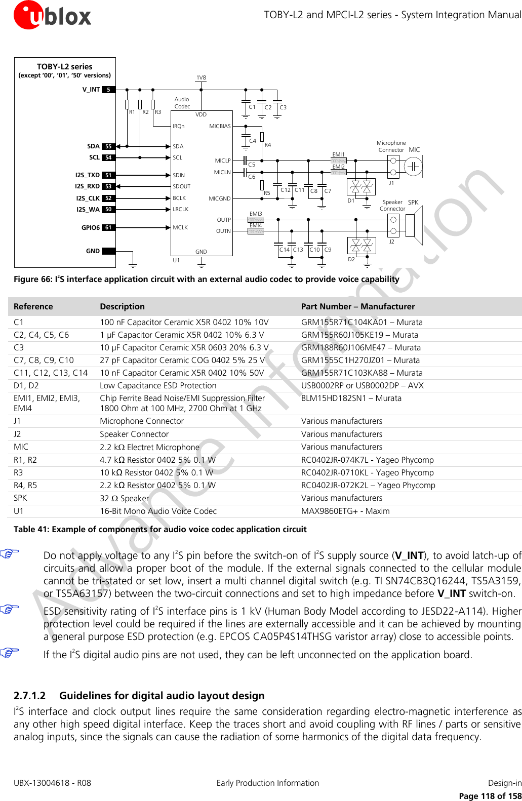
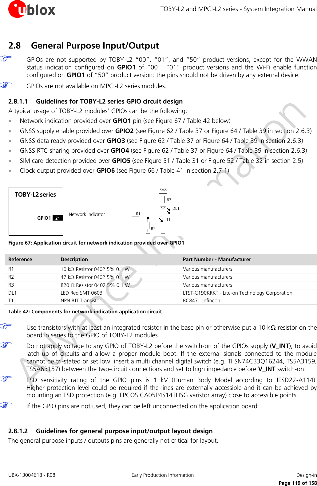
![TOBY-L2 and MPCI-L2 series - System Integration Manual UBX-13004618 - R08 Early Production Information Design-in Page 121 of 158 2.9.1.2 Guidelines for LED_WWAN# circuit design As described in Figure 69 and Table 44, the MPCI-L2 series modules LED_WWAN# active-low open drain output can be directly connected to a system-mounted LED to provide the Wireless Wide Area Network status indication as specified by the PCI Express Mini Card Electromechanical Specification [15]. Open Drain OutputR3V3DL42LED_WWAN#MPCI-L2 series Figure 69: LED_WWAN# application circuit Reference Description Remarks DL LED Green SMT 0603 LTST-C190KGKT - Lite-on Technology Corporation R 470 Resistor 0402 5% 0.1 W Various manufacturers Table 44: Example of components for the LED_WWAN# application circuit ESD sensitivity rating of the LED_WWAN# pin is 1 kV (Human Body Model according to JESD22-A114). Higher protection level could be required if the line is externally accessible and it can be achieved by mounting an ESD protection (e.g. EPCOS CA05P4S14THSG varistor) close to accessible point. If the LED_WWAN# functionality is not required by the application, the pin can be left unconnected. 2.9.1.3 Guidelines for W_DISABLE# and LED_WWAN# layout design The W_DISABLE# and LED_WWAN# circuits are generally not critical for layout. 2.10 Reserved pins (RSVD) Pins reserved for future use, marked as RSVD, are not available on MPCI-L2 series. TOBY-L2 series modules have pins reserved for future use. All the RSVD pins are to be left unconnected on the application board except the RSVD pin number 6 which must be connected to ground as described in Figure 70. TOBY-L2 seriesRSVD6RSVD Figure 70: Application circuit for the reserved pins (RSVD)](https://usermanual.wiki/u-blox/TOBYL280.System-Integrators-Manual/User-Guide-2664029-Page-121.png)
![TOBY-L2 and MPCI-L2 series - System Integration Manual UBX-13004618 - R08 Early Production Information Design-in Page 124 of 158 2.13 MPCI-L2 series module installation MPCI-L2 series modules are fully compliant with the 52-pin PCI Express Full-Mini Card Type F2 form factor, i.e., top-side and bottom-side keep-out areas, 50.95 mm nominal length, 30 mm nominal width, and all the other dimensions as defined by the PCI Express Mini Card Electromechanical Specification [15], except for the card thickness (which nominal value is 3.7 mm), as described in Figure 72. 3.7 mmSide ViewPin 1 Pin 51ANT1ANT2Top ViewHole GND HoleGND 30 mmPin 52 Pin 2Bottom ViewHole GND HoleGND50.95 mm Figure 72: MPCI-L2 series mechanical description (top, side and bottom views) MPCI-L2 series modules are fully compliant with the 52-pin PCI Express Full-Mini card edge type system connector as defined by the PCI Express Mini Card Electromechanical Specification [15]. Table 46 describes some examples of 52-pin mating system connectors for the MPCI-L2 series PCI Express Full-Mini card modules. Manufacturer Part Number Description JAE Electronics MM60 series 52-circuit, 0.8 mm pitch, PCI Express Mini card edge female connector Molex 67910 series 52-circuit, 0.8 mm pitch, PCI Express Mini card edge female connector TE Connectivity / AMP 2041119 series 52-circuit, 0.8 mm pitch, PCI Express Mini card edge female connector FCI 10123824 series 52-circuit, 0.8 mm pitch, PCI Express Mini card edge female connector Table 46: MPCI-L2 series PCI Express Full-Mini card compatible connector It is recommended to use the two mounting holes described in Figure 72 to fix (ground) the MPCI-L2 module to the main ground of the application board with suitable screws and fasteners. Follow the recommendations provided by the connector manufacturer and the guidelines available in the PCI Express Mini Card Electromechanical Specification [15] for the development of the footprint (i.e. the copper mask) PCB layout for the mating edge system connector. The exact geometries, distances and stencil thicknesses should be adapted to the specific production processes (e.g. soldering etc.). Follow the recommendations provided by the connector manufacturer to properly insert and remove the MPCI-L2 series modules.](https://usermanual.wiki/u-blox/TOBYL280.System-Integrators-Manual/User-Guide-2664029-Page-124.png)
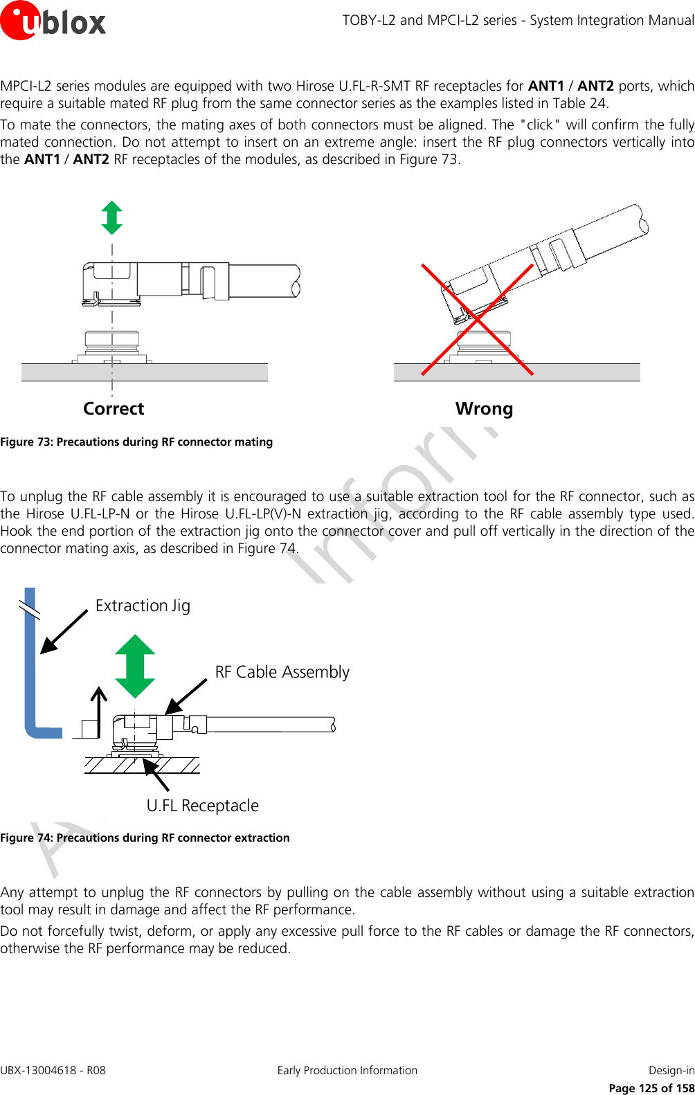
![TOBY-L2 and MPCI-L2 series - System Integration Manual UBX-13004618 - R08 Early Production Information Design-in Page 126 of 158 2.14 Thermal guidelines Modules’ operating temperature range is specified in TOBY-L2 Data Sheet [1] and MPCI-L2 Data Sheet [2]. The most critical condition concerning module thermal performance is the uplink transmission at maximum power (data upload in connected-mode), when the baseband processor runs at full speed, radio circuits are all active and the RF power amplifier is driven to higher output RF power. This scenario is not often encountered in real networks (for example, see the Terminal Tx Power distribution for WCDMA, taken from operation on a live network, described in the GSMA TS.09 Battery Life Measurement and Current Consumption Technique [21]); however the application should be correctly designed to cope with it. During transmission at maximum RF power the TOBY-L2 and MPCI-L2 series modules generate thermal power that may exceed 3 W: this is an indicative value since the exact generated power strictly depends on operating condition such as the actual antenna return loss, the number of allocated TX resource blocks, the transmitting frequency band, etc. The generated thermal power must be adequately dissipated through the thermal and mechanical design of the application. The spreading of the Module-to-Ambient thermal resistance (Rth,M-A) depends on the module operating condition. The overall temperature distribution is influenced by the configuration of the active components during the specific mode of operation and their different thermal resistance toward the case interface. The Module-to-Ambient thermal resistance value and the relative increase of module temperature will differ according to the specific mechanical deployments of the module, e.g. application PCB with different dimensions and characteristics, mechanical shells enclosure, or forced air flow. The increase of the thermal dissipation, i.e. the reduction of the Module-to-Ambient thermal resistance, will decrease the temperature of the modules’ internal circuitry for a given operating ambient temperature. This improves the device long-term reliability in particular for applications operating at high ambient temperature. A few hardware techniques may be used to reduce the Module-to-Ambient thermal resistance in the application: Connect each GND pin with solid ground layer of the application board and connect each ground area of the multilayer application board with complete thermal via stacked down to main ground layer. Use the two mounting holes described in Figure 72 to fix (ground) the MPCI-L2 modules to the main ground of the application board with suitable screws and fasteners. Provide a ground plane as wide as possible on the application board. Optimize antenna return loss, to optimize overall electrical performance of the module including a decrease of module thermal power. Optimize the thermal design of any high-power components included in the application, such as linear regulators and amplifiers, to optimize overall temperature distribution in the application device. Select the material, the thickness and the surface of the box (i.e. the mechanical enclosure) of the application device that integrates the module so that it provides good thermal dissipation. Force ventilation air-flow within mechanical enclosure. Provide a heat sink component attached to the module top side, with electrically insulated / high thermal conductivity adhesive, or on the backside of the application board, below the cellular module, as a large part of the heat is transported through the GND pads of the TOBY-L2 series LGA modules and dissipated over the backside of the application board. Follow the thermal guidelines for integrating wireless wide area network mini card add-in cards, such as the MPCI-L2 series modules, as provided in the PCI Express Mini Card Electromechanical Specification [15]](https://usermanual.wiki/u-blox/TOBYL280.System-Integrators-Manual/User-Guide-2664029-Page-126.png)
![TOBY-L2 and MPCI-L2 series - System Integration Manual UBX-13004618 - R08 Early Production Information Design-in Page 127 of 158 For example, the Module-to-Ambient thermal resistance (Rth,M-A) is strongly reduced with forced air ventilation and a heat-sink installed on the back of the application board, decreasing the module temperature variation. Beside the reduction of the Module-to-Ambient thermal resistance implemented by proper application hardware design, the increase of module temperature can be moderated by proper application software implementation: Enable power saving configuration using the AT+UPSV command (see section 1.15.18). Enable module connected-mode for a given time period and then disable it for a time period enough long to properly mitigate temperature increase. 2.15 ESD guidelines The sections 2.15.1 and 2.15.2 are related to EMC / ESD immunity. The modules are ESD sensitive devices. The ESD sensitivity for each pin (as Human Body Model according to JESD22-A114F) is specified in TOBY-L2 series Data Sheet [1] or MPCI-L2 series Data Sheet [2]. Special precautions are required when handling the pins; for ESD handling guidelines see section 3.2. 2.15.1 ESD immunity test overview The immunity of devices integrating TOBY-L2 and MPCI-L2 series modules to Electro-Static Discharge (ESD) is part of the Electro-Magnetic Compatibility (EMC) conformity which is required for products bearing the CE marking, compliant with the R&TTE Directive (99/5/EC), the EMC Directive (89/336/EEC) and the Low Voltage Directive (73/23/EEC) issued by the Commission of the European Community. Compliance with these directives implies conformity to the following European Norms for device ESD immunity: ESD testing standard CENELEC EN 61000-4-2 [22] and the radio equipment standards ETSI EN 301 489-1 [23], ETSI EN 301 489-7 [24], ETSI EN 301 489-24 [25], which requirements are summarized in Table 47. The ESD immunity test is performed at the enclosure port, defined by ETSI EN 301 489-1 [23] as the physical boundary through which the electromagnetic field radiates. If the device implements an integral antenna, the enclosure port is seen as all insulating and conductive surfaces housing the device. If the device implements a removable antenna, the antenna port can be separated from the enclosure port. The antenna port includes the antenna element and its interconnecting cable surfaces. The applicability of ESD immunity test to the whole device depends on the device classification as defined by ETSI EN 301 489-1 [23]. Applicability of ESD immunity test to the relative device ports or the relative interconnecting cables to auxiliary equipment, depends on device accessible interfaces and manufacturer requirements, as defined by ETSI EN 301 489-1 [23]. Contact discharges are performed at conductive surfaces, while air discharges are performed at insulating surfaces. Indirect contact discharges are performed on the measurement setup horizontal and vertical coupling planes as defined in CENELEC EN 61000-4-2 [22]. For the definition of integral antenna, removable antenna, antenna port and device classification see ETSI EN 301 489-1 [23]. For the contact / air discharges definitions see CENELEC EN 61000-4-2 [22]. Application Category Immunity Level All exposed surfaces of the radio equipment and ancillary equipment in a representative configuration Contact Discharge 4 kV Air Discharge 8 kV Table 47: EMC / ESD immunity requirements as defined by CENELEC EN 61000-4-2 and ETSI EN 301 489-1, 301 489-7, 301 489-24](https://usermanual.wiki/u-blox/TOBYL280.System-Integrators-Manual/User-Guide-2664029-Page-127.png)
![TOBY-L2 and MPCI-L2 series - System Integration Manual UBX-13004618 - R08 Early Production Information Design-in Page 128 of 158 2.15.2 ESD immunity test of TOBY-L2 and MPCI-L2 series reference designs Although EMC / ESD certification is required for customized devices integrating TOBY-L2 and MPCI-L2 series modules for R&TTED and European Conformance CE mark, EMC certification (including ESD immunity) has been successfully performed on TOBY-L2 and MPCI-L2 series modules reference design according to European Norms summarized in Table 47. The EMC / ESD approved u-blox reference designs consist of a TOBY-L2 and MPCI-L2 series module installed onto a motherboard which provides supply interface, SIM card and communication port. External LTE/3G/2G antennas are connected to the provided connectors. Since external antennas are used, the antenna port can be separated from the enclosure port. The reference design is not enclosed in a box so that the enclosure port is not identified with physical surfaces. Therefore, some test cases cannot be applied. Only the antenna port is identified as accessible for direct ESD exposure. Table 48 reports the u-blox TOBY-L2 and MPCI-L2 series reference designs ESD immunity test results, according to test requirements stated in the CENELEC EN 61000-4-2 [22], ETSI EN 301 489-1 [23], ETSI EN 301 489-7 [24] and ETSI EN 301 489-24 [25]. Category Application Immunity Level Remarks Contact Discharge to coupling planes (indirect contact discharge) Enclosure +4 kV / -4 kV Contact Discharges to conducted surfaces (direct contact discharge) Enclosure port Not Applicable Test not applicable to u-blox reference design because it does not provide enclosure surface. The test is applicable only to equipment providing conductive enclosure surface. Antenna ports +4 kV / -4 kV Test applicable to u-blox reference design because it provides antennas with conductive & insulating surfaces. The test is applicable only to equipment providing antennas with conductive surface. Air Discharge at insulating surfaces Enclosure port Not Applicable Test not applicable to the u-blox reference design because it does not provide an enclosure surface. The test is applicable only to equipment providing insulating enclosure surface. Antenna ports +8 kV / -8 kV Test applicable to u-blox reference design because it provides antennas with conductive & insulating surfaces. The test is applicable only to equipment providing antennas with insulating surface. Table 48: Enclosure ESD immunity level of u-blox TOBY-L2 and MPCI-L2 series modules reference designs TOBY-L2 and MPCI-L2 reference design implement all the ESD precautions described in section 2.15.3. 2.15.3 ESD application circuits The application circuits described in this section are recommended and should be implemented in the device integrating TOBY-L2 and MPCI-L2 series modules, according to the application device classification (see ETSI EN 301 489-1 [23]), to satisfy the requirements for ESD immunity test summarized in Table 47. Antenna interface The ANT1 and ANT2 ports of TOBY-L2 and MPCI-L2 series modules provide ESD immunity up to ±4 kV for direct Contact Discharge and up to ±8 kV for Air Discharge: no further precaution to ESD immunity test is needed, as implemented in the EMC / ESD approved reference design of TOBY-L2 and MPCI-L2 series modules.](https://usermanual.wiki/u-blox/TOBYL280.System-Integrators-Manual/User-Guide-2664029-Page-128.png)
![TOBY-L2 and MPCI-L2 series - System Integration Manual UBX-13004618 - R08 Early Production Information Design-in Page 129 of 158 The antenna interface application circuit implemented in the EMC / ESD approved reference designs of TOBY-L2 and MPCI-L2 series modules is described in Figure 47 in case of antennas detection circuit not implemented, and is described in Figure 48 and Table 28 in case of antennas detection circuit implemented (section 2.4). RESET_N and PERST# pin The following precautions are suggested for the RESET_N and the PERST# line of TOBY-L2 and MPCI-L2 series modules, depending on the application board handling, to satisfy ESD immunity test requirements: It is recommended to keep the connection line to RESET_N and PERST# as short as possible Maximum ESD sensitivity rating of the RESET_N and the PERST# pin is 1 kV (Human Body Model according to JESD22-A114). Higher protection level could be required if the RESET_N or PERST# pin is externally accessible on the application board. The following precautions are suggested to achieve higher protection level: A general purpose ESD protection device (e.g. EPCOS CA05P4S14THSG varistor array or EPCOS CT0402S14AHSG varistor) should be mounted on the RESET_N or PERST# line, close to accessible point The RESET_N and PERST# application circuit implemented in the EMC / ESD approved reference designs of TOBY-L2 and MPCI-L2 series modules is described in Figure 42 and Table 23 (section 2.3.2). SIM interface The following precautions are suggested for TOBY-L2 and MPCI-L2 series modules SIM interface, depending on the application board handling, to satisfy ESD immunity test requirements: A bypass capacitor of about 22 pF to 47 pF (e.g. Murata GRM1555C1H470J) must be mounted on the lines connected to the SIM interface pins to assure SIM interface functionality when an electrostatic discharge is applied to the application board enclosure It is suggested to use as short as possible connection lines at SIM pins Maximum ESD sensitivity rating of SIM interface pins is 1 kV (Human Body Model according to JESD22-A114). Higher protection level could be required if SIM interface pins are externally accessible on the application board. The following precautions are suggested to achieve higher protection level: A low capacitance (i.e. less than 10 pF) ESD protection device (e.g. Tyco Electronics PESD0402-140) should be mounted on each SIM interface line, close to accessible points (i.e. close to the SIM card holder) The SIM interface application circuit implemented in the EMC / ESD approved reference designs of TOBY-L2 and MPCI-L2 series modules is described in Figure 49 and Table 29 (section 2.5). Other pins and interfaces All the module pins that are externally accessible on the device integrating TOBY-L2 and MPCI-L2 series module should be included in the ESD immunity test since they are considered to be a port as defined in ETSI EN 301 489-1 [23]. Depending on applicability, to satisfy ESD immunity test requirements according to ESD category level, all the module pins that are externally accessible should be protected up to ±4 kV for direct Contact Discharge and up to ±8 kV for Air Discharge applied to the enclosure surface. The maximum ESD sensitivity rating of all the other pins of the module is 1 kV (Human Body Model according to JESD22-A114). Higher protection level could be required if the relative pin is externally accessible on the application board. The following precautions are suggested to achieve higher protection level: USB interface: a very low capacitance (i.e. less or equal to 1 pF) ESD protection device (e.g. Tyco Electronics PESD0402-140 ESD protection device) should be mounted on the USB_D+ and USB_D- lines, close to the accessible points (i.e. close to the USB connector) Other pins: a general purpose ESD protection device (e.g. EPCOS CA05P4S14THSG varistor array or EPCOS CT0402S14AHSG varistor) should be mounted on the related line, close to accessible point](https://usermanual.wiki/u-blox/TOBYL280.System-Integrators-Manual/User-Guide-2664029-Page-129.png)
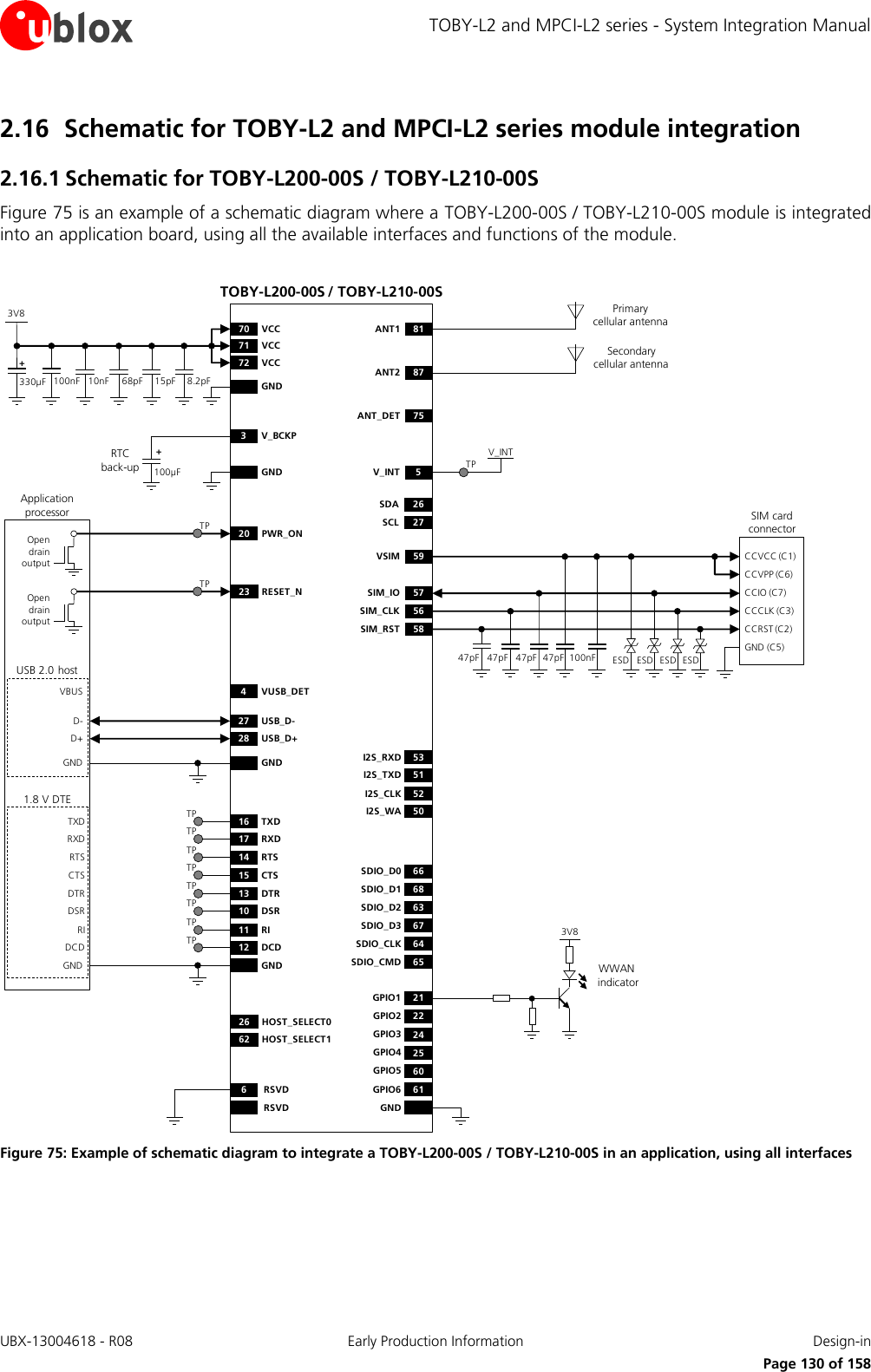
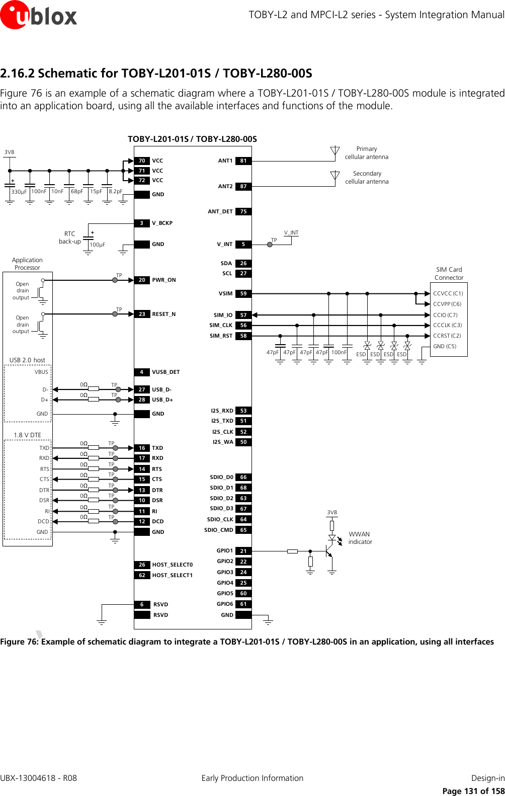
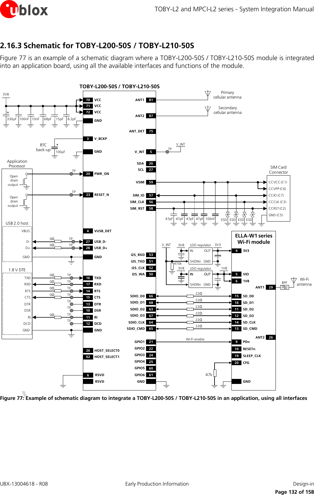
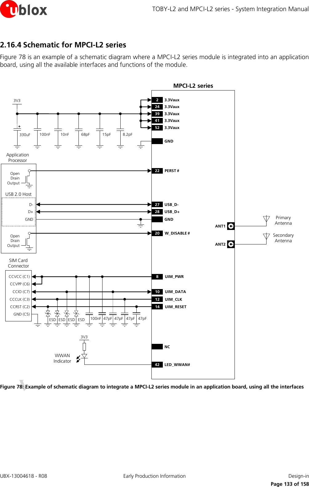
![TOBY-L2 and MPCI-L2 series - System Integration Manual UBX-13004618 - R08 Early Production Information Design-in Page 134 of 158 2.17 Design-in checklist This section provides a design-in checklist. 2.17.1 Schematic checklist The following are the most important points for a simple schematic check: DC supply must provide a nominal voltage at VCC / 3.3Vaux pin within the operating range limits. DC supply must be capable of supporting both the highest peak and the highest averaged current consumption values in connected-mode, as specified in the TOBY-L2 series Data Sheet [1] or in the MPCI-L2 series Data Sheet [2]. VCC / 3.3Vaux voltage supply should be clean, with very low ripple/noise: provide the suggested bypass capacitors, in particular if the application device integrates an internal antenna. Do not apply loads which might exceed the limit for maximum available current from V_INT supply. Check that voltage level of any connected pin does not exceed the relative operating range. Check USB_D+ / USB_D- signal lines as well as very low capacitance ESD protections if accessible. Capacitance and series resistance must be limited on each SIM signal to match the SIM specifications. Insert the suggested capacitors on each SIM signal and low capacitance ESD protections if accessible. Check UART signals direction, as the TOBY-L2 signal names follow the ITU-T V.24 Recommendation [7]. Consider providing appropriate low value series damping resistors on SDIO lines to avoid reflections. Provide accessible test points directly connected to the following pins of the TOBY-L2 series modules: V_INT, PWR_ON and RESET_N for diagnostic purpose. Provide accessible test points directly connected to all the UART pins of the TOBY-L2 series modules (TXD, RXD, RTS, CTS, DTR, DSR, DCD, RI) for diagnostic purpose, in particular providing a 0 series jumper on each line to detach each UART pin of the module from the DTE application processor. If the USB is not used, provide accessible test points directly connected to the USB_D+ and USB_D- pins Provide proper precautions for EMC / ESD immunity as required on the application board. Do not apply voltage to any generic digital interface pin of TOBY-L2 series modules before the switch-on of the generic digital interface supply source (V_INT). All unused pins can be left unconnected except the RSVD pin number 6 of TOBY-L2 series modules, which must be connected to GND.](https://usermanual.wiki/u-blox/TOBYL280.System-Integrators-Manual/User-Guide-2664029-Page-134.png)
![TOBY-L2 and MPCI-L2 series - System Integration Manual UBX-13004618 - R08 Early Production Information Design-in Page 135 of 158 2.17.2 Layout checklist The following are the most important points for a simple layout check: Check 50 nominal characteristic impedance of the RF transmission line connected to the ANT1 and the ANT2 ports (antenna RF interfaces). Ensure no coupling occurs between the RF interface and noisy or sensitive signals (primarily USB signals, digital input/output signals, SIM signals, high-speed digital lines such as SDIO and other data lines). Optimize placement for minimum length of RF line. Check the footprint and paste mask designed for TOBY-L2 module as illustrated in section 2.12. VCC / 3.3Vaux line should be wide and as short as possible. Route VCC / 3.3Vaux supply line away from RF lines / parts and other sensitive analog lines / parts. The VCC / 3.3Vaux bypass capacitors in the picoFarad range should be placed as close as possible to the VCC / 3.3Vaux pins, in particular if the application device integrates an internal antenna. Ensure an optimal grounding connecting each GND pin with application board solid ground layer. Use as many vias as possible to connect the ground planes on multilayer application board, providing a dense line of vias at the edges of each ground area, in particular along RF and high speed lines. Keep routing short and minimize parasitic capacitance on the SIM lines to preserve signal integrity. USB_D+ / USB_D- traces should meet the characteristic impedance requirement (90 differential and 30 common mode) and should not be routed close to any RF line / part. Keep the SDIO traces short, avoid stubs, avoid coupling with any RF line / part and consider low value series damping resistors to avoid reflections and other losses in signal integrity. Ensure appropriate RF precautions for the Wi-Fi and Cellular technologies coexistence as described in section 2.6.4 and in the Wi-Fi / Cellular Integration Application Note [14]. Ensure appropriate RF precautions for the GNSS and Cellular technologies coexistence as described in the GNSS Implementation Application Note [13]. 2.17.3 Antenna checklist Antenna termination should provide 50 characteristic impedance with V.S.W.R at least less than 3:1 (recommended 2:1) on operating bands in deployment geographical area. Follow the recommendations of the antenna producer for correct antenna installation and deployment (PCB layout and matching circuitry). Ensure compliance with any regulatory agency RF radiation requirement, as reported in section 4.2.2 for products marked with the FCC. Ensure high and similar efficiency for both the primary (ANT1) and the secondary (ANT2) antenna. Ensure high isolation between the primary (ANT1) and the secondary (ANT2) antenna. Ensure low Envelope Correlation Coefficient between the primary (ANT1) and the secondary (ANT2) antenna: the 3D antenna radiation patterns should have radiation lobes in different directions. Ensure high isolation between the cellular antennas and any other antenna or transmitter.](https://usermanual.wiki/u-blox/TOBYL280.System-Integrators-Manual/User-Guide-2664029-Page-135.png)
![TOBY-L2 and MPCI-L2 series - System Integration Manual UBX-13004618 - R08 Early Production Information Handling and soldering Page 136 of 158 3 Handling and soldering No natural rubbers, no hygroscopic materials or materials containing asbestos are employed. 3.1 Packaging, shipping, storage and moisture preconditioning For information pertaining to TOBY-L2 series reels / tapes, MPCI-L2 series trays, Moisture Sensitivity levels (MSD), shipment and storage information, as well as drying for preconditioning, see the TOBY-L2 series Data Sheet [1], the MPCI-L2 series Data Sheet [2] and the u-blox Package Information Guide [31]. 3.2 Handling The TOBY-L2 and MPCI-L2 series modules are Electro-Static Discharge (ESD) sensitive devices. Ensure ESD precautions are implemented during handling of the module. Electrostatic discharge (ESD) is the sudden and momentary electric current that flows between two objects at different electrical potentials caused by direct contact or induced by an electrostatic field. The term is usually used in the electronics and other industries to describe momentary unwanted currents that may cause damage to electronic equipment. The ESD sensitivity for each pin of TOBY-L2 and MPCI-L2 series modules (as Human Body Model according to JESD22-A114F) is specified in the TOBY-L2 series Data Sheet [1] or the MPCI-L2 series Data Sheet [2]. ESD prevention is based on establishing an Electrostatic Protective Area (EPA). The EPA can be a small working station or a large manufacturing area. The main principle of an EPA is that there are no highly charging materials near ESD sensitive electronics, all conductive materials are grounded, workers are grounded, and charge build-up on ESD sensitive electronics is prevented. International standards are used to define typical EPA and can be obtained for example from International Electrotechnical Commission (IEC) or American National Standards Institute (ANSI). In addition to standard ESD safety practices, the following measures should be taken into account whenever handling the TOBY-L2 and MPCI-L2 series modules: Unless there is a galvanic coupling between the local GND (i.e. the work table) and the PCB GND, then the first point of contact when handling the PCB must always be between the local GND and PCB GND. Before mounting an antenna patch, connect ground of the device. When handling the module, do not come into contact with any charged capacitors and be careful when contacting materials that can develop charges (e.g. patch antenna, coax cable, soldering iron,…). To prevent electrostatic discharge through the RF pin, do not touch any exposed antenna area. If there is any risk that such exposed antenna area is touched in non ESD protected work area, implement proper ESD protection measures in the design. When soldering the module and patch antennas to the RF pin, make sure to use an ESD safe soldering iron. For more robust designs, employ additional ESD protection measures on the application device integrating the TOBY-L2 and MPCI-L2 series modules, as described in section 2.15.3.](https://usermanual.wiki/u-blox/TOBYL280.System-Integrators-Manual/User-Guide-2664029-Page-136.png)
![TOBY-L2 and MPCI-L2 series - System Integration Manual UBX-13004618 - R08 Early Production Information Handling and soldering Page 138 of 158 To avoid falling off, modules should be placed on the topside of the motherboard during soldering. The soldering temperature profile chosen at the factory depends on additional external factors like choice of soldering paste, size, thickness and properties of the base board, etc. Exceeding the maximum soldering temperature and the maximum liquidus time limit in the recommended soldering profile may permanently damage the module. Preheat Heating Cooling[°C] Peak Temp. 245°C [°C]250 250Liquidus Temperature217 217200 20040 - 60 sEnd Temp.max 4°C/s150 - 200°C150 150max 3°C/s60 - 120 s100 Typical Leadfree 100Soldering Profile50 50Elapsed time [s] Figure 79: Recommended soldering profile The modules must not be soldered with a damp heat process. 3.3.3 Optical inspection After soldering the TOBY-L2 series modules, inspect the modules optically to verify that the module is properly aligned and centered. 3.3.4 Cleaning Cleaning the modules is not recommended. Residues underneath the modules cannot be easily removed with a washing process. Cleaning with water will lead to capillary effects where water is absorbed in the gap between the baseboard and the module. The combination of residues of soldering flux and encapsulated water leads to short circuits or resistor-like interconnections between neighboring pads. Water will also damage the sticker and the ink-jet printed text. Cleaning with alcohol or other organic solvents can result in soldering flux residues flooding into the two housings, areas that are not accessible for post-wash inspections. The solvent will also damage the sticker and the ink-jet printed text. Ultrasonic cleaning will permanently damage the module, in particular the quartz oscillators. For best results use a "no clean" soldering paste and eliminate the cleaning step after the soldering.](https://usermanual.wiki/u-blox/TOBYL280.System-Integrators-Manual/User-Guide-2664029-Page-138.png)
![TOBY-L2 and MPCI-L2 series - System Integration Manual UBX-13004618 - R08 Early Production Information Approvals Page 140 of 158 4 Approvals For the complete list of all the certification schemes approvals of TOBY-L2 and MPCI-L2 series modules and the corresponding declarations of conformity, see the u-blox web-site (http://www.u-blox.com/). 4.1 Product certification approval overview Product certification approval is the process of certifying that a product has passed all tests and criteria required by specifications, typically called “certification schemes” that can be divided into three distinct categories: Regulatory certification o Country specific approval required by local government in most regions and countries, such as: CE (Conformité Européenne) marking for European Union FCC (Federal Communications Commission) approval for United States Industry certification o Telecom industry specific approval verifying the interoperability between devices and networks: GCF (Global Certification Forum), partnership between European device manufacturers and network operators to ensure and verify global interoperability between devices and networks PTCRB (PCS Type Certification Review Board), created by United States network operators to ensure and verify interoperability between devices and North America networks Operator certification o Operator specific approval required by some mobile network operator, such as: AT&T network operator in United States Even if TOBY-L2 and MPCI-L2 series modules are approved under all major certification schemes, the application device that integrates TOBY-L2 and MPCI-L2 series modules must be approved under all the certification schemes required by the specific application device to be deployed in the market. The required certification scheme approvals and relative testing specifications differ depending on the country or the region where the device that integrates TOBY-L2 and MPCI-L2 series modules must be deployed, on the relative vertical market of the device, on type, features and functionalities of the whole application device, and on the network operators where the device must operate. The certification of the application device that integrates a TOBY-L2 module and the compliance of the application device with all the applicable certification schemes, directives and standards are the sole responsibility of the application device manufacturer. TOBY-L2 and MPCI-L2 series modules are certified according to all capabilities and options stated in the Protocol Implementation Conformance Statement document (PICS) of the module. The PICS, according to the 3GPP TS 51.010-2 [26], 3GPP TS 34.121-2 [27], 3GPP TS 36.521-2 [28] and 3GPP TS 36.523-2 [29], is a statement of the implemented and supported capabilities and options of a device. The PICS document of the application device integrating TOBY-L2 and MPCI-L2 series modules must be updated from the module PICS statement if any feature stated as supported by the module in its PICS document is not implemented or disabled in the application device. For more details regarding the AT commands settings that affect the PICS, see the u-blox AT Commands Manual [3]. Check the specific settings required for mobile network operators approvals as they may differ from the AT commands settings defined in the module as integrated in the application device.](https://usermanual.wiki/u-blox/TOBYL280.System-Integrators-Manual/User-Guide-2664029-Page-140.png)
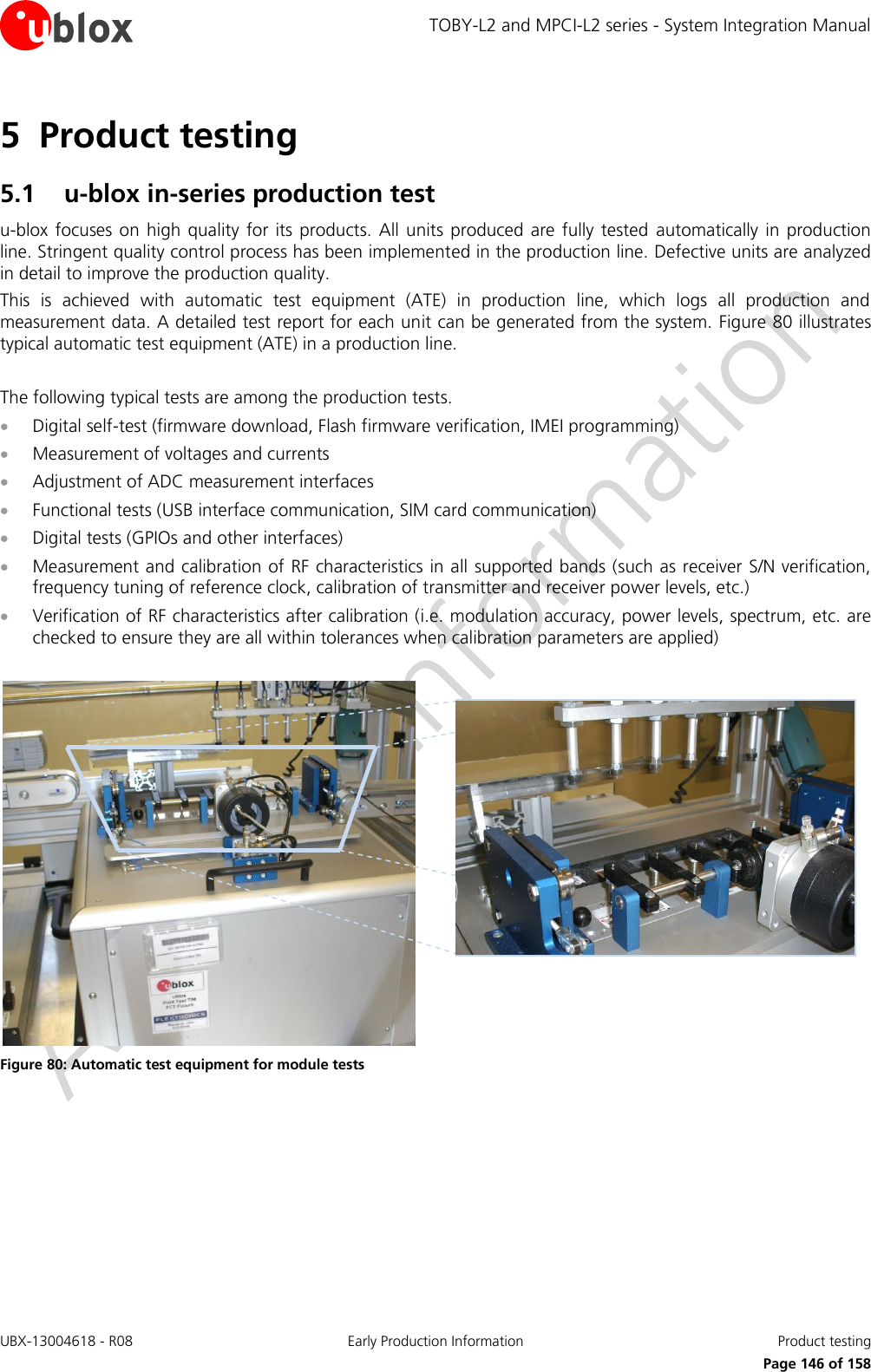
![TOBY-L2 and MPCI-L2 series - System Integration Manual UBX-13004618 - R08 Early Production Information Product testing Page 147 of 158 5.2 Test parameters for OEM manufacturer Because of the testing done by u-blox (with 100% coverage), an OEM manufacturer does not need to repeat firmware tests or measurements of the module RF performance or tests over analog and digital interfaces in their production test. However, an OEM manufacturer should focus on: Module assembly on the device; it should be verified that: o Soldering and handling process did not damage the module components o All module pins are well soldered on device board o There are no short circuits between pins Component assembly on the device; it should be verified that: o Communication with host controller can be established o The interfaces between module and device are working o Overall RF performance test of the device including antenna Dedicated tests can be implemented to check the device. For example, the measurement of module current consumption when set in a specified status can detect a short circuit if compared with a “Golden Device” result. In addition, module AT commands can be used to perform functional tests (communication with host controller, check SIM interface, GPIOs, etc.) and to perform RF performance tests: see the following two sections for details. 5.2.1 “Go/No go” tests for integrated devices A “Go/No go” test is typically to compare the signal quality with a “Golden Device” in a location with excellent network coverage and known signal quality. This test should be performed after data connection has been established. AT+CSQ is the typical AT command used to check signal quality in term of RSSI. See the u-blox AT Commands Manual [3] for detail usage of the AT command. These kinds of test may be useful as a “go/no go” test but not for RF performance measurements. This test is suitable to check the functionality of communication with host controller, SIM card as well as power supply. It is also a means to verify if components at antenna interface are well soldered. 5.2.2 RF functional tests The overall RF functional test of the device including the antenna can be performed with basic instruments such as a spectrum analyzer (or an RF power meter) and a signal generator with the assistance of AT+UTEST command over AT command user interface. The AT+UTEST command provides a simple interface to set the module to Rx or Tx test modes ignoring the LTE/3G/2G signaling protocol. The command can set the module into: transmitting mode in a specified channel and power level in all supported modulation schemes and bands receiving mode in a specified channel to returns the measured power level in all supported bands See the u-blox AT Commands Manual [3] and the End user test Application Note [26], for the AT+UTEST command syntax description and detail guide of usage.](https://usermanual.wiki/u-blox/TOBYL280.System-Integrators-Manual/User-Guide-2664029-Page-147.png)
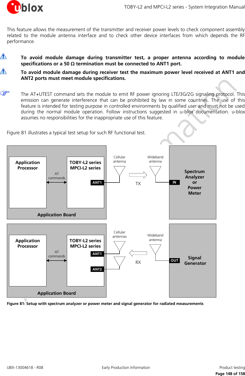
![TOBY-L2 and MPCI-L2 series - System Integration Manual UBX-13004618 - R08 Early Production Information Appendix Page 151 of 158 B Migration between TOBY-L1 and TOBY-L2 B.1 Overview TOBY-L1 and TOBY-L2 series cellular modules have exactly the same TOBY form factor (35.6 x 24.8 mm LGA) with exactly the same 152-pin layout as described in Figure 82, so that the modules can be alternatively mounted on a single application board using exactly the same copper mask, solder mask and paste mask. 11107542121191816151312292726242386322201714282596566697172747555575860616364474950525368707354565962485167RSVDRSVDGNDVCCVCCGNDRSVDRSVDSIM_IOSIM_RSTGPIO5GPIO6RSVDRSVDRSVDRSVDRSVDRSVDRSVDRSVDVCCGNDRSVDSIM_CLKVSIMRSVDRSVDRSVDRSVDRSVDRSVDRSVDV_INTRSVDGNDRSVDGPIO1RSVDRSVDRSVDRSVDRSVDRSVDRSVDUSB_D-RSVDGPIO3RESET_NRSVDRSVDV_BCKPGPIO2PWR_ONRSVDRSVDUSB_D+GPIO4RSVD90 91 927877769310079 80 83 85 86 88 8982 84 8781GNDRSVDGNDGNDRSVDGNDGNDGNDGNDGNDGNDGNDGNDGNDRSVDANT2ANT132 31 3044454614515243 42 39 37 36 34 3340 38 3541GNDRSVDGNDGNDRSVDGNDRSVDRSVDRSVDRSVDRSVDRSVDRSVDRSVDRSVDRSVDRSVD99 98 97 96 95 94106 105 104 103 102 101108 107124 123130 129 128 127 126 125136 135 134 133 132 131138 137144 143 142 141 140 139151 150 149 148 147 146114 113 112 111 110 109120 119 118 117 116 115122 121Pin 93-152: GNDTOBY-L1Top view11107542121191816151312292726242386322201714282596566697172747555575860616364474950525368707354565962485167SDIO_CMDSDIO_D0GNDVCCVCCGNDANT_DETSDASIM_IOSIM_RSTGPIO5GPIO6SDIO_D2SDIO_CLKRSVDRSVDI2S_WAI2S_CLKI2S_RXDSDIO_D1VCCGNDSCLSIM_CLKVSIMHOST_SELECT1RSVDI2S_TXDSDIO_D3RIDSRRSVDV_INTVUSB_DETGNDRSVDGPIO1RSVDRSVDTXDCTSDTRDCDRSVDUSB_D-HOST_SELECT0GPIO3RESET_NRSVDRSVDV_BCKPGPIO2PWR_ONRXDRTSUSB_D+GPIO4RSVD90 91 927877769310079 80 83 85 86 88 8982 84 8781GNDRSVDGNDGNDRSVDGNDGNDGNDGNDGNDGNDGNDGNDGNDRSVDANT2ANT132 31 3044454614515243 42 39 37 36 34 3340 38 3541GNDRSVDGNDGNDRSVDGNDRSVDRSVDRSVDRSVDRSVDRSVDRSVDRSVDRSVDRSVDRSVD99 98 97 96 95 94106 105 104 103 102 101108 107124 123130 129 128 127 126 125136 135 134 133 132 131138 137144 143 142 141 140 139151 150 149 148 147 146114 113 112 111 110 109120 119 118 117 116 115122 121Pin 93-152: GNDTOBY-L2Top view Figure 82: TOBY-L1 and TOBY-L2 series modules pad layout and pin assignment TOBY modules are also form-factor compatible with the u-blox LISA and SARA cellular module families: although TOBY modules, LISA modules (33.2 x 22.4 mm, 76-pin LCC) and SARA modules (26.0 x 16.0 mm, 96-pin LGA) each have different form factors, the footprints for the TOBY, LISA and SARA modules have been developed to ensure layout compatibility. With the u-blox “nested design” solution, any TOBY, LISA or SARA module can be alternatively mounted on the same space of a single “nested” application board as described in Figure 83. Guidelines in order to implement a nested application board, description of the u-blox reference design as nested application board and comparison between TOBY, LISA and SARA modules are provided in the Nested Design Application Note [32]. TOBY cellular moduleLISA cellular moduleSARA cellular moduleNested application board Figure 83: TOBY, LISA, SARA modules’ layout compatibility: the nested design accommodates all modules on the same footprint](https://usermanual.wiki/u-blox/TOBYL280.System-Integrators-Manual/User-Guide-2664029-Page-151.png)
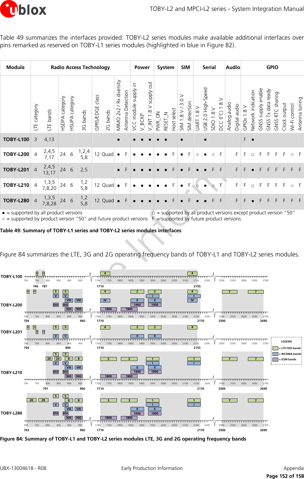
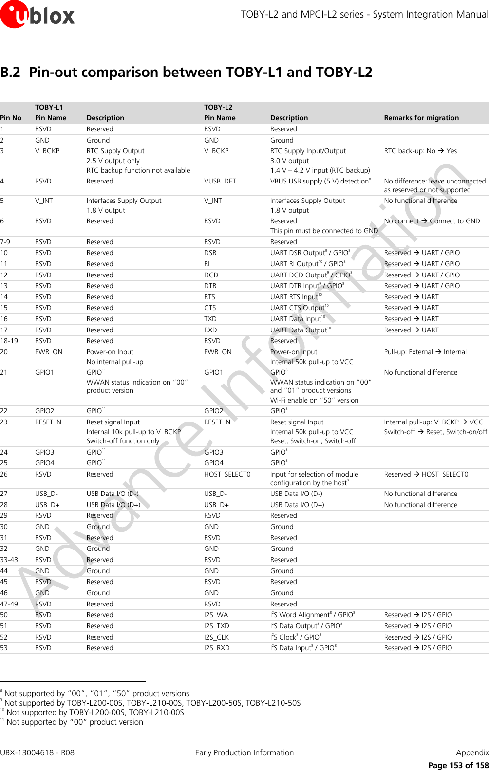
![TOBY-L2 and MPCI-L2 series - System Integration Manual UBX-13004618 - R08 Early Production Information Appendix Page 154 of 158 TOBY-L1 TOBY-L2 Pin No Pin Name Description Pin Name Description Remarks for migration 54 RSVD Reserved SCL I2C Clock Output12 Reserved I2C 55 RSVD Reserved SDA I2C Data I/O12 Reserved I2C 56 SIM_CLK SIM Clock Output SIM_CLK SIM Clock Output No functional difference 57 SIM_IO SIM Data I/O SIM_IO SIM Data I/O No functional difference 58 SIM_RST SIM Reset Output SIM_RST SIM Reset Output No functional difference 59 VSIM SIM Supply Output VSIM SIM Supply Output No functional difference 60 GPIO5 GPIO13 GPIO5 GPIO12 SIM detection 61 GPIO6 GPIO13 GPIO6 GPIO12 62 RSVD Reserved HOST_SELECT1 Input for selection of module configuration by the host12 Reserved HOST_SELECT1 63 RSVD Reserved SDIO_D2 SDIO serial data [2]14 Reserved SDIO 64 RSVD Reserved SDIO_CLK SDIO serial clock14 Reserved SDIO 65 RSVD Reserved SDIO_CMD SDIO command14 Reserved SDIO 66 RSVD Reserved SDIO_D0 SDIO serial data [0]14 Reserved SDIO 67 RSVD Reserved SDIO_D3 SDIO serial data [3]14 Reserved SDIO 68 RSVD Reserved SDIO_D1 SDIO serial data [1]14 Reserved SDIO 69 GND Ground GND Ground 70-72 VCC Module Supply Input 3.40 V – 4.50 V normal range No 2G current pulses No switch-on applying VCC VCC Module Supply Input 3.40 V – 4.35 V normal range High 2G current pulses Switch-on applying VCC No VCC functional difference 73-74 GND Ground GND Ground 75 RSVD Reserved ANT_DET Antenna Detection Input12 Reserved ANT_DET 76 GND Ground GND Ground 77 RSVD Reserved RSVD Reserved 78-80 GND Ground GND Ground 81 ANT1 RF Antenna Input/Output Two LTE bands No 3G bands No 2G bands ANT1 RF Antenna Input/Output Up to six LTE bands Up to five 3G bands Four 2G bands No RF functional difference Different operating bands support 82-83 GND Ground GND Ground 84 RSVD Reserved RSVD Reserved 85-86 GND Ground GND Ground 87 ANT2 RF Antenna Input LTE MIMO 2x2 No 3G Rx diversity ANT2 RF Antenna Input LTE MIMO 2x2 3G Rx diversity No RF functional difference Different operating bands support 88-90 GND Ground GND Ground 91 RSVD Reserved RSVD Reserved 92-152 GND Ground GND Ground Table 50: TOBY-L1 and TOBY-L2 pin assignment with remarks for migration 12 Not supported by “00”, “01”, “50” product versions 13 Not supported by “00” product version 14 Not supported by “00”, “01” product versions](https://usermanual.wiki/u-blox/TOBYL280.System-Integrators-Manual/User-Guide-2664029-Page-154.png)
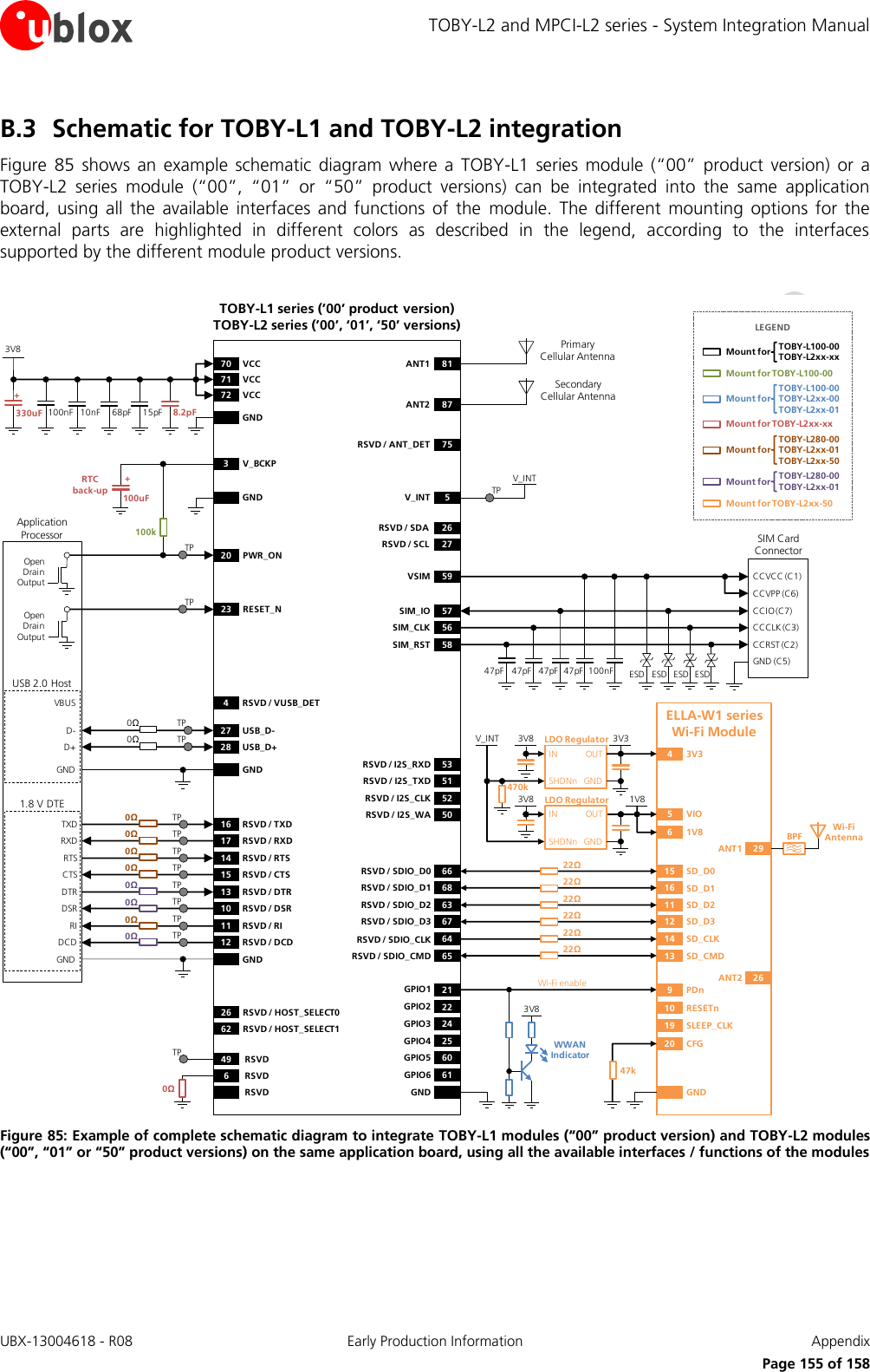
![TOBY-L2 and MPCI-L2 series - System Integration Manual UBX-13004618 - R08 Early Production Information Related documents Page 156 of 158 Related documents [1] u-blox TOBY-L2 series Data Sheet, Docu No UBX-13004573 [2] u-blox MPCI-L2 series Data Sheet, Docu No UBX-13004749 [3] u-blox AT Commands Manual, Docu No UBX-13002752 [4] u-blox EVK-L20 / EVK-L21 User Guide, Docu No UBX-14000422 [5] u-blox Firmware Update Application Note, Docu No UBX-13001845 [6] Universal Serial Bus Revision 2.0 specification, http://www.usb.org/developers/docs/usb20_docs/ [7] ITU-T Recommendation V.24 - 02-2000 - List of definitions for interchange circuits between Data Terminal Equipment (DTE) and Data Circuit-terminating Equipment (DCE), http://www.itu.int/rec/T-REC-V.24-200002-I/en [8] 3GPP TS 27.007 - AT command set for User Equipment (UE) [9] 3GPP TS 27.005 - Use of Data Terminal Equipment - Data Circuit terminating; Equipment (DTE - DCE) interface for Short Message Service (SMS) and Cell Broadcast Service (CBS) [10] 3GPP TS 27.010 - Terminal Equipment to User Equipment (TE-UE) multiplexer protocol [11] u-blox Mux Implementation Application Note, Docu No UBX-13001887 [12] I2C-bus specification and user manual - Rev. 5 - 9 October 2012 - NXP Semiconductors, http://www.nxp.com/documents/user_manual/UM10204.pdf [13] u-blox GNSS Implementation Application Note, Docu No UBX-13001849 [14] u-blox Wi-Fi / Cellular Integration Application Note, Docu No UBX-14003264 [15] PCI Express Mini Card Electromechanical Specification, Revision 2.0, April 21, 2012 [16] 3GPP TS 26.267 – eCall Data Transfer; In-band modem solution; General description [17] BS EN 16062:2011 – Intelligent transport systems – eSafety – eCall high level application requirements [18] ETSI TS 122 101 – Service aspects; Service principles (3GPP TS 22.101) [19] u-blox eCall / ERA-GLONASS Application Note, Docu No UBX-13001924 [20] SIM Access Profile Interoperability Specification, http://www.bluetooth.org/ [21] GSM Association TS.09 - Battery Life Measurement and Current Consumption Technique http://www.gsma.com/newsroom/wp-content/uploads/2013/09/TS.09-v7.6.pdf [22] CENELEC EN 61000-4-2 (2001): "Electromagnetic compatibility (EMC) – Part 4-2: Testing and measurement techniques – Electrostatic discharge immunity test". [23] ETSI EN 301 489-1 V1.8.1: “Electromagnetic compatibility and Radio spectrum Matters (ERM); EMC standard for radio equipment and services; Part 1: Common technical requirements” [24] ETSI EN 301 489-7 V1.3.1 “Electromagnetic compatibility and Radio spectrum Matters (ERM); EMC standard for radio equipment and services; Part 7: Specific conditions for mobile and portable radio and ancillary equipment of digital cellular radio telecommunications systems“ [25] ETSI EN 301 489-24 V1.4.1 "Electromagnetic compatibility and Radio spectrum Matters (ERM); EMC standard for radio equipment and services; Part 24: Specific conditions for IMT-2000 CDMA Direct Spread (UTRA) for Mobile and portable (UE) radio and ancillary equipment" [26] 3GPP TS 51.010-2 - Technical Specification Group GSM/EDGE Radio Access Network; Mobile Station (MS) conformance specification; Part 2: Protocol Implementation Conformance Statement (PICS) [27] 3GPP TS 34.121-2 - Technical Specification Group Radio Access Network; User Equipment (UE) conformance specification; Radio transmission and reception (FDD); Part 2: Implementation Conformance Statement (ICS) [28] 3GPP TS 36.521-2 - Evolved Universal Terrestrial Radio Access (E-UTRA); User Equipment conformance specification; Radio transmission and reception; Part 2: Implementation Conformance Statement (ICS) [29] 3GPP TS 36.523-2 - Evolved Universal Terrestrial Radio Access (E-UTRA) and Evolved Packet Core (EPC); User Equipment conformance specification; Part 2: Implementation Conformance Statement (ICS) [30] u-blox End user test Application Note, Docu No UBX-13001922 [31] u-blox Package Information Guide, Docu No UBX-14001652 [32] u-blox Nested Design Application Note, Docu No UBX-13002795 Some of the above documents can be downloaded from u-blox web-site (http://www.u-blox.com/).](https://usermanual.wiki/u-blox/TOBYL280.System-Integrators-Manual/User-Guide-2664029-Page-156.png)