u blox VERAP174 Host-based V2X transceiver module User Manual Antenna trace layout
u-blox AG Host-based V2X transceiver module Antenna trace layout
UserManual.wiki
>
u blox
>
VERAP174 User Manual
>
Antenna trace layout
Contents
1.
Antenna trace layout
2.
User Manual
Antenna trace layout
Navigation menu
Upload a User Manual
Namespaces
Wiki Guide
HTML
PDF
Info
Views
User Manual
Discussion / Help
Navigation
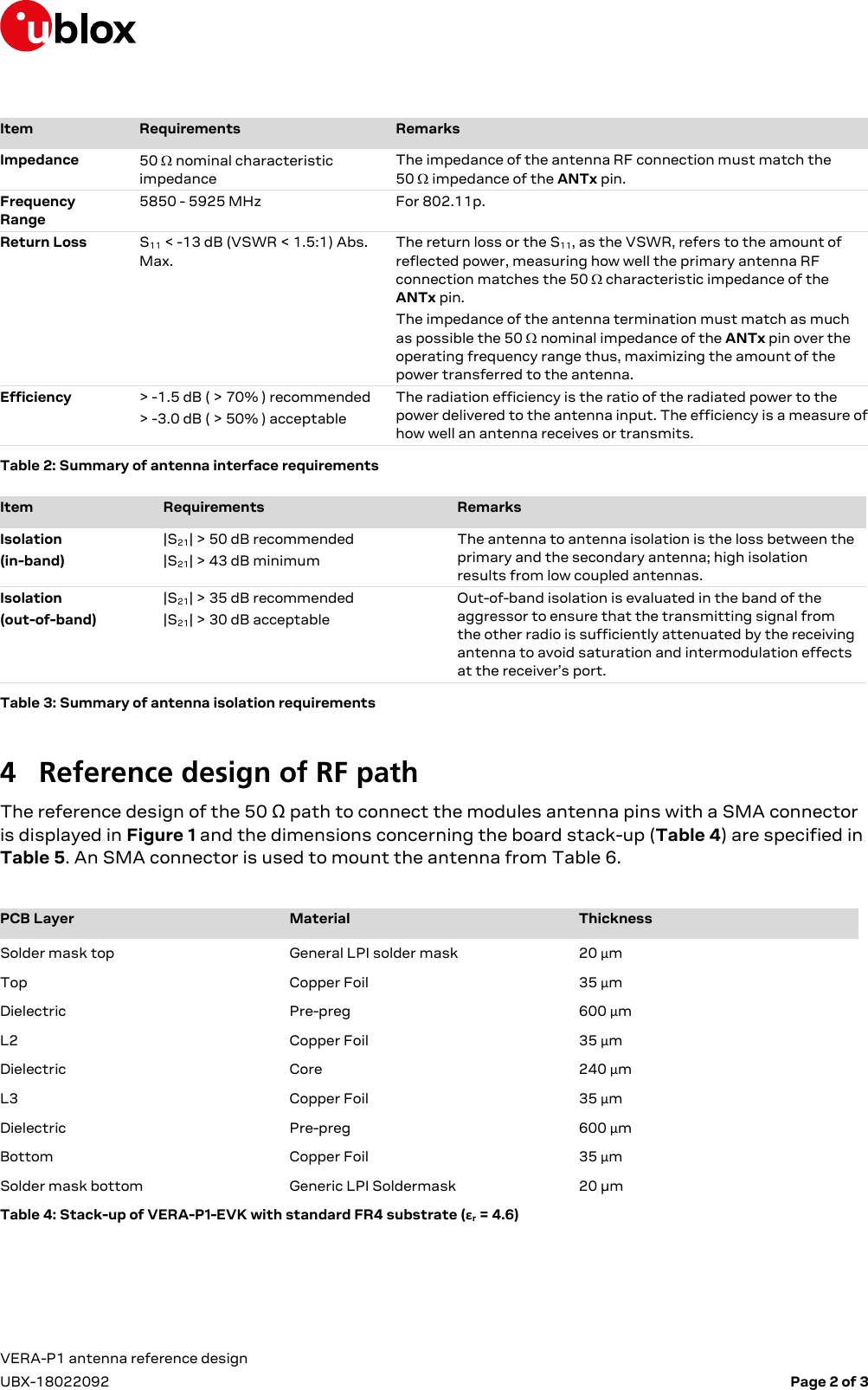
![VERA-P1 antenna reference design UBX-18022092 Page 3 of 3 Figure 1: Coplanar waveguide with ground dimension specification Item Value S 400 µm W 900 µm T 35 µm H 600 µm Spacing between ANT1 and ANT2 waveguides 16 mm Table 5: Coplanar waveguide with ground specification 5 Antenna The module has been approved for use with any dipole antenna with less or equal to 6 dBi peak gain. An example of an approved antenna is listed in Table 6. Model name Manufacturer and description Gain [dBi] (peak) TD.10.5113 Taoglas, Dipole Terminal Antenna SMA Connector 5.88 dBi Table 6: Approved antenna example](https://usermanual.wiki/u-blox/VERAP174.Antenna-trace-layout/User-Guide-3919004-Page-3.png)