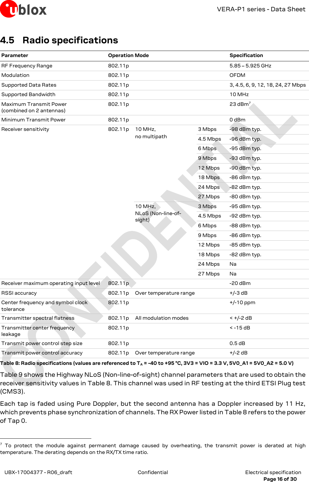
u blox VERAP174 Host-based V2X transceiver module User Manual VERA P1 series
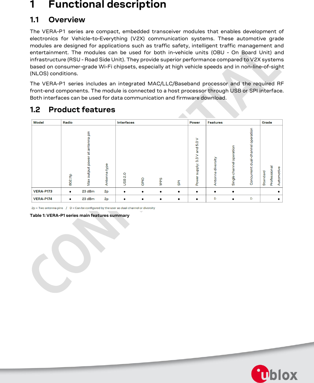
u-blox AG Host-based V2X transceiver module VERA P1 series
UserManual.wiki
>
u blox
>
VERAP174 User Manual
>
User Manual
Contents
1.
Antenna trace layout
2.
User Manual
User Manual
Navigation menu
Upload a User Manual
Namespaces
Wiki Guide
HTML
PDF
Info
Views
User Manual
Discussion / Help
Navigation
![VERA-P1 series - Data Sheet UBX-17004377 - R06_draft Qualification and approvals Page 20 of 30 Confidential 6 Qualification and approvals 6.1 Approvals8 Products marked with this lead-free symbol on the product label comply with the "Directive 2002/95/EC of the European Parliament and the Council on the Restriction of Use of certain Hazardous Substances in Electrical and Electronic Equipment" (RoHS). VERA-P1 series V2X modules are RoHS compliant. 6.1.1 European Union regulatory compliance TBD 6.1.2 FCC compliance The VERA-P1 series modules comply with Part 95, Subpart L and Part 90, Subpart M of the FCC Rules. Operation is subject to the following two conditions: 1. This device may not cause harmful interference, and 2. This device must accept any interference received, including interference that may cause undesired operation. ⚠ Non authorized modification could void authority to use this equipment. The internal / external antenna(s) used for this module must provide a separation distance of at least 20 cm from all persons and must not be co-located or operating in conjunction with any other antenna or transmitter. These limits are designed to provide reasonable protection against harmful interference in a residential installation. This equipment generates, uses and can radiate radio frequency energy and, if not installed and used in accordance with the manufacturer’s instructions, may cause harmful interference to radio communications. ☞ The outside of final product that contains the VERA-P173 or VERA-P174 module must display in a user accessible area a label referring to the enclosed module. This exterior label can use wording such as the following: “Contains Transmitter Module FCC ID: XPYVERAP174” or “Contains FCC ID: XPYVERAP174”. 6.1.3 FCC IDs Model FCC ID VERA-P173 XPYVERAP174 VERA-P174 XPYVERAP174 Table 14: FCC IDs for different models of VERA-P1 series 6.1.4 Certification in other countries TBD 6.2 Approved antennas Please refer to the VERA-P1 series antenna reference design [2] for the essential specifications to be fulfilled in the end-product design to make use of the module’s radio type approval. It provides PCB layout details and electrical specifications as well as information about approved antennas. 8 These approvals are pending.](https://usermanual.wiki/u-blox/VERAP174.User-Manual/User-Guide-3919019-Page-20.png)
![VERA-P1 series - Data Sheet UBX-17004377 - R06_draft Product handling & soldering Page 22 of 30 Confidential 7 Product handling & soldering 7.1 Packaging The VERA-P1 series modules are delivered as hermetically sealed, reeled tapes to enable efficient production, production lot set-up and tear-down. For more information about packaging, see the u-blox Package Information Guide [1]. 7.1.1 Reels The VERA-P1 series modules are deliverable in quantities of 250 pieces on a reel. The VERA-P1 series modules are shipped on reel Type A as specified in the u-blox Package Information Guide [1]. 7.1.2 Tapes Figure 4 shows the position and orientation of the VERA-P1 modules as they are delivered on tape. The dimensions of the tapes are specified in Figure 5. Figure 4: Orientation of VERA-P1 module on tape Figure 5: VERA-P1 tape dimensions Feed direction](https://usermanual.wiki/u-blox/VERAP174.User-Manual/User-Guide-3919019-Page-22.png)
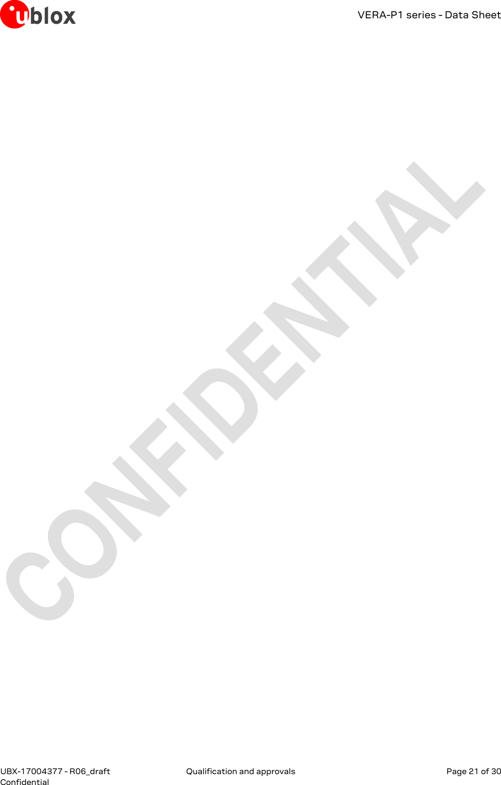
![VERA-P1 series - Data Sheet UBX-17004377 - R06_draft Product handling & soldering Page 23 of 30 Confidential 7.2 Shipment, storage and handling For more information regarding shipment, storage and handling see the u-blox Package Information Guide [1]. 7.2.1 Moisture sensitivity levels The VERA-P1 series modules are rated at moisture sensitivity level 3. See moisture sensitive warning label on each shipping bag for detailed information. After opening the dry pack, modules must be mounted within 168 hours in factory conditions of maximum 30 °C/60%RH or must be stored at less than 10%RH. Modules require baking if the humidity indicator card shows more than 10% when read at 23±5°C or if the conditions mentioned above are not met. Please refer to J-STD-033B standard for bake procedure. 7.2.2 Mounting process and soldering recommendations The VERA-P1 series module is a surface mount module supplied on an 8-layer FR4-type PCB with gold plated connection pins and produced in a lead-free process with a lead-free soldering paste. The wrap page of the PCB is max. 0.75% according to IPC-A-610E. The thickness of solder resist on the host PCB top side and the JODY-W1 bottom side must be considered for the soldering process. This module is compatible with industrial reflow profile for RoHS/Pb-free solders, Sn96.5/Ag3.0/Cu0.5 solder is a right choice. Use of "No Clean" soldering paste is strongly recommended, cleaning the populated modules is strongly discouraged - residuals under the module cannot be easily removed with any cleaning process. Cleaning with water can lead to capillary effects where water is absorbed into the gap between the host board and module. The combination of soldering flux residuals and encapsulated water could lead to short circuits between neighboring pins. Only a single reflow soldering process is permitted for host boards with the VERA-P1 series modules. The reflow profile used is dependent on the thermal mass of the entire populated PCB, heat transfer efficiency of the oven and particular type of solder paste used. Since the profile used is process and layout dependent, the optimum profile should be studied case by case. Recommendations below should be taken as a starting point guide. In case of basic information necessity, refer to J-STD-020C standard. Profile feature Sn-Pb eutectic (Sn63/Pb37) RoHS/Pb-free (Sn96.5/Ag3.0/Cu0.5) Ramp up rate (TSMAX to TP) 3 °C/sec max 3 °C/sec max Minimum soak temperature (TSMIN) 100 °C 150 °C Maximum soak temperature (TSMAX) 150 °C 200 °C Soak time (ts) 60 - 120 sec 60 - 180 sec Liquidus temperature (TL) 183 °C 217 °C Time above TL (tL) 60 - 150 sec 60 - 150 sec Peak temperature (TP) 215 – 225 °C 235 – 245 °C Time within +0 / -5°C of actual TP (tp) 10 - 30 sec 20 - 40 sec Ramp down rate 6 °C/sec max 6 °C/sec max Time from 25°C to TP 6 min max 8 min max Table 15: Recommended reflow profile ☞ The lowest value of TP and slower ramp down rate (2 – 3 °C/sec) is preferred.](https://usermanual.wiki/u-blox/VERAP174.User-Manual/User-Guide-3919019-Page-23.png)
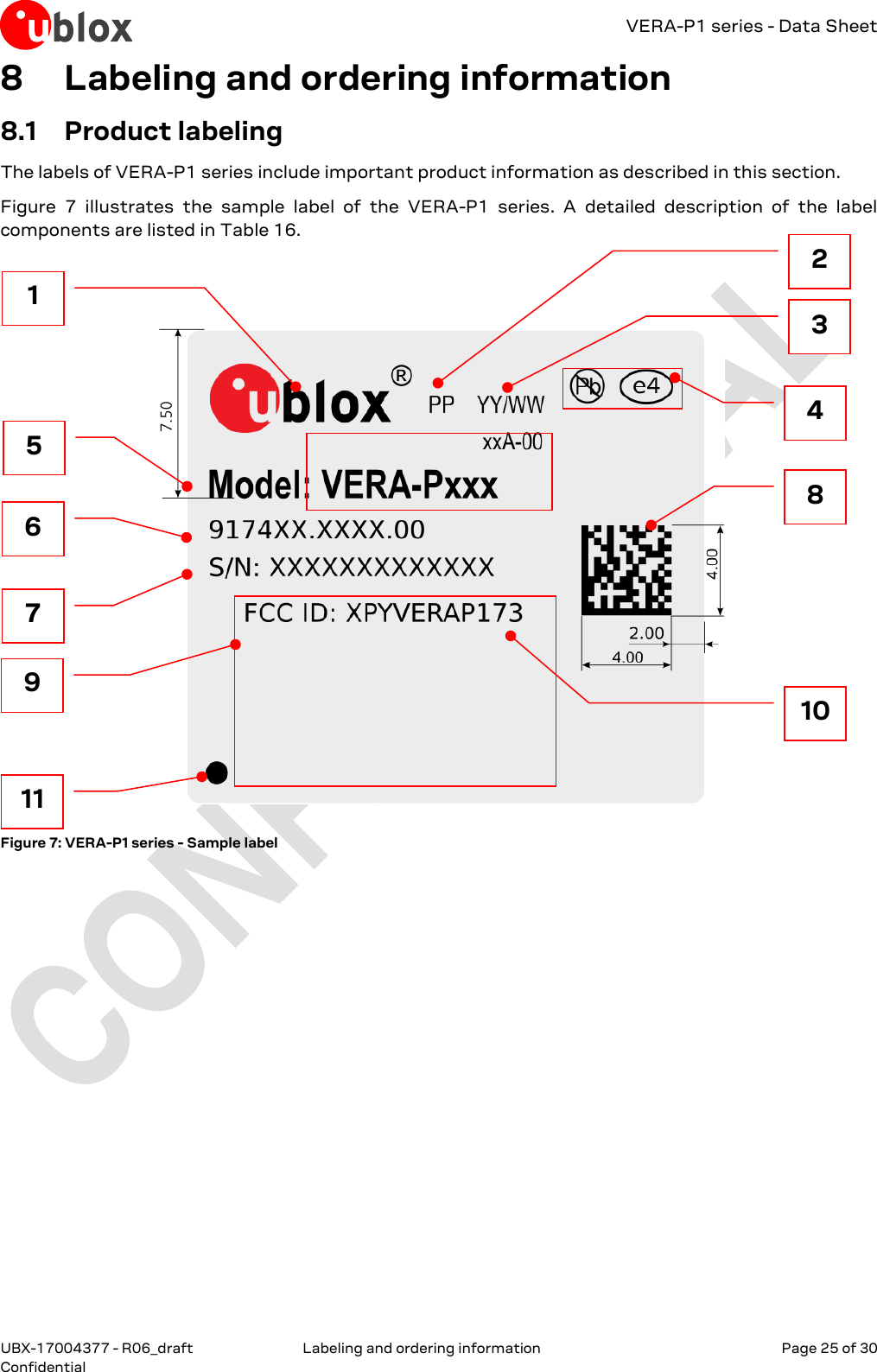
![VERA-P1 series - Data Sheet UBX-17004377 - R06_draft Labeling and ordering information Page 26 of 30 Confidential Reference Description 1 Company logo and trademark 2 Panel position number 3 Production date YY/WW (year/week) 4 Pb-Free, Platin Spec IPC-1066/JESD97 5 Type number (format PPPP-TGVV-TTQ-XX), e.g. VERA-P173-00A-00 “Model:” PPPP-TGVV TTQ-XX 6 Datacode 7 Serial number “S/N:” MAC address (Format of MAC address: D4-CA-6E-01-02-03) 8 DataMatrix (product identifier, serial number, datacode) Product identifier: 3 digits Serial number: MAC address Datacode: 4 digits 9 Text box containing approval IDs 10 FCC ID: XPYVERA173 (example) 11 Pin 1 marker Table 16: VERA-P1 series label description 8.2 Explanation of codes Three different product code formats are used. The Product Name is used in documentation such as this data sheet and identifies all u-blox products, independent of packaging and quality grade. The Ordering Code includes options and quality, while the Type Number includes the hardware and firmware versions. Table 17 below details these three different formats: Format Structure Product Name PPPP-TGVV Ordering Code PPPP-TGVV-TTQ Type Number PPPP-TGVV-TTQ-XX Table 17: Product Code Formats Code Meaning Example PPPP Form factor VERA TG Platform T – Dominant technology, For example, W: Wi-Fi, B: Bluetooth G – Generation P1 VV Variant based on the same platform; range [00…99] 73 TT Major Product Version 00 Q Quality grade A: Automotive B: Professional C: Standard A XX Minor product version (not relevant for certification) 00 Table 18: Part identification code](https://usermanual.wiki/u-blox/VERAP174.User-Manual/User-Guide-3919019-Page-26.png)
![VERA-P1 series - Data Sheet UBX-17004377 - R06_draft Related documents Page 29 of 30 Confidential Related documents [1] u-blox Package Information Guide, document number UBX-14001652 [2] VERA-P1 series antenna reference design, document number UBX-18022092 ☞ For regular updates to u-blox documentation and to receive product change notifications, register on our homepage (www.u-blox.com). Revision history Revision Date Name Comments R01 23-Feb-2017 ishe, kgom Initial release. R02 5-May-2017 ddie, kgom Added VERA-P174 product variant and included block diagram, FCC/IC ID, and ordering code for this variant. R03 11-Sep-2017 mzes, kgom, ddie Updated Table 1. Included footnotes in section 1.5. Updated the ordering codes (section 8.3). Added reel size (section 7.1) and tape dimensions (Figure 5). R04 17-Oct-2017 ddie, kgom Removed references to VERA-P175 variant. Updated Table 1. R05 4-June-2018 smay, kgom Updated total power consumption in section 1.5. Added SPI limitation in section 2.2. Added peak current consumption in Table 7. Extended worst case dimension D in section 5.1. Added position and orientation in section 7.1.2. Added product labeling in section 8.1. Update lowest TX power level. Removed all references to VERA-P171 variant. R06 22-June-2018 ddie Added clarification that 23 dBm max output power is the combined output power of two antennas. Added FCC approvals section (6.1.2).](https://usermanual.wiki/u-blox/VERAP174.User-Manual/User-Guide-3919019-Page-29.png)