u blox WIBEAR11N-DF1 WLAN & Bluetooth Module User Manual WiBear11n DS
u-blox AG WLAN & Bluetooth Module WiBear11n DS
u blox >
Contents
user manual

The information in this document is subject to change without notice. Please download latest version from www.lesswire.com
Copyright © 2013 lesswire AG
www.lesswire.com
WiBear11n
IEEE 802.11a/b/g/n WLAN, Bluetooth 3.0+EDR Module
Data Sheet
Version 1.18
December 2013
WiBear11n Data Sheet
Version 1.18
Copyright © 2013 lesswire AG
www.lesswire.com
Page 2 of 20
Introduction
The WiBear11n industrial universal module is targeted
for integration into different OEM products. The module
is designed for both simultaneous and independent
operation of the following:
IEEE 802.11a/b/g/n payload data rates for Wireless
Local Area Network (WLAN), Bluetooth 3.0+High
Speed (HS) and Bluetooth 2.1+EDR.
It provides a complete end-to-end solution for low-
power applications. It includes an integrated
MAC/Baseband processor and RF front-end
components and can connect to a host processor
through an SDIO interface.
The WiBear11n modules are offered in four versions
(see ordering information and block diagram).
Host drivers for common operating systems such as
Linux and Windows 7 are available.
The modules are radio type approved for Europe (CE),
US (FCC) and Industry Canada (IC) (pending).
Applications
WLAN and Bluetooth networks
Audio/video devices and accessories
Access to laptops, mobile phones etc.
Automotive and industrial networking
Home / building automation
Key Features
Standards: IEEE 802.11a/b/g/n/e/i/h/d/k/r/w
WLAN 802.11a/b/g/n station and micro access point operation (up to 8 clients supported)
Support of Wi-Fi direct mode
802.11n 1x1 SISO
802.11 PHY data rates up to 72 Mbps (20 MHz channel) and up to 150 Mbps (40 MHz channel)
Hardware 64- and 128-bit encryption AES engine performance
Embedded security supplicant
WAPI encryption is supported by hardware
Background scan mode
Bluetooth 3.0 + HS (High Speed)
Bluetooth 2.1 + EDR (backward compatibility)
Wide temperature operation range -40ºC to +85ºC
Compact 14.8mm x 14.8mm footprint, surface mounting
SDIO high-speed interface
Support for low-power modes
CE/FCC/IC compliant
RoHS compliant
Automotive qualification tests (climatic, mechanical, and operating life tests) according to VW 80000 /
ISO 16750-4 (report pending)
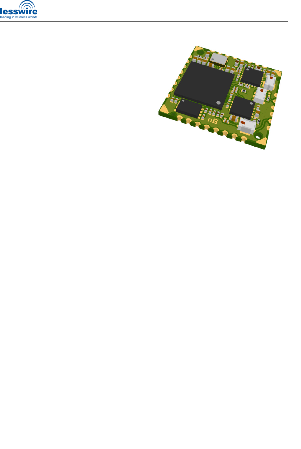
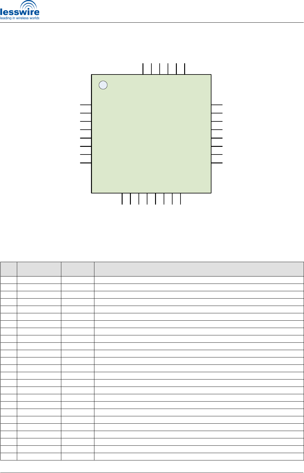
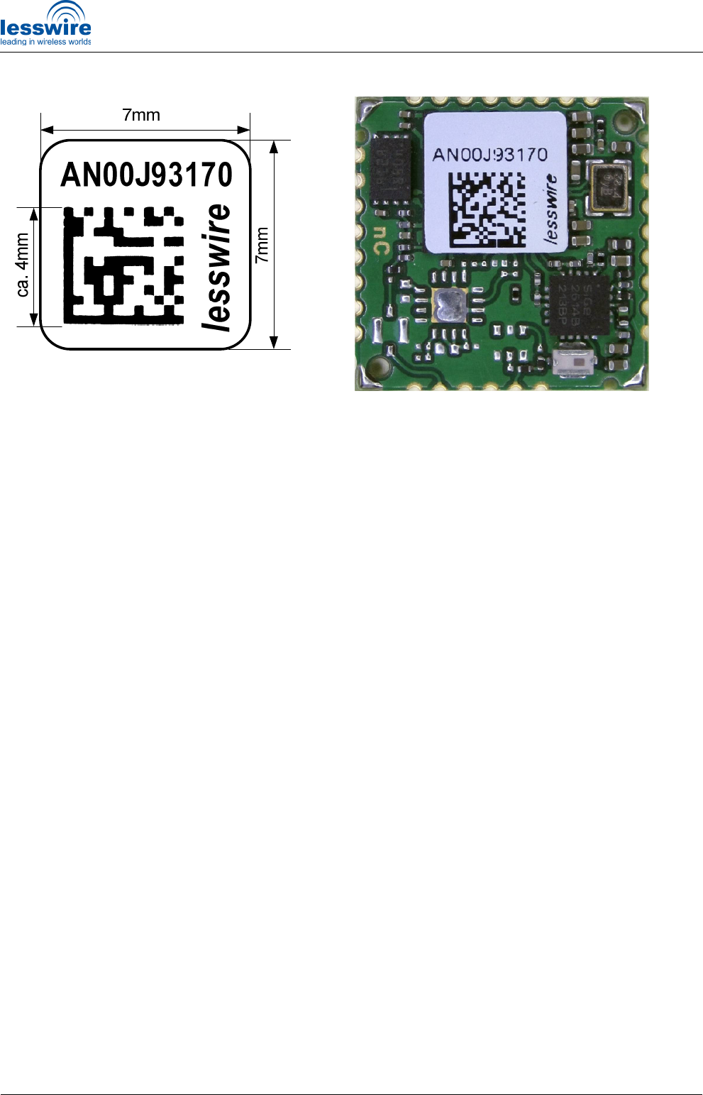
Figure 1: Physical outlook
WiBear11n Data Sheet
Version 1.18
Copyright © 2013 lesswire AG
www.lesswire.com
Page 3 of 20
Ordering Information
Table 1: Ordering information
Order Number Model Description
AN00J93170 WiBear11n-SF1 WiBear-SF1 Module
AN00J93174 WiBear11n-SF2 WiBear-SF2 Module
AN00J93172 WiBear11n-DF1 WiBear-DF1 Module
AN00J93176 WiBear11n-DF2 WiBear-DF2 Module
AN00J94359 WiBear11n-SF1 WiBear-SF1 Module, tape&reel package (500 pcs)
AN00J94361 WiBear11n-SF2 WiBear-SF2 Module, tape&reel package (500 pcs)
AN00J94360 WiBear11n-DF1 WiBear-DF1 Module, tape&reel package (500 pcs)
AN00J94362 WiBear11n-DF2 WiBear-DF2 Module, tape&reel package (500 pcs)
AN00J93704 WiBear11n-DF1_EK Evaluation Kit with WiBear11n-DF1 Module
AN00J93705 WiBear11n-DF2_EK Evaluation Kit with WiBear11n-DF2 Module
Note: Shielded modules available on special request.
IMDS number: 355902511
Customs Tariff Numbers:
HTC / TARIC: 85177090
ECCN number: 3A001
EORI no.: DE4665759
Product Variants
Table 2: Product variants
Model Description
WiBear11n-SF1 Single band WLAN (802.11 b/g/n, 2.4 GHz only) and Bluetooth module. Module has one
joint antenna connector for WLAN and Bluetooth operation (see block diagram).
WiBear11n-SF1/-DF1 is recommended for cost effective AP solution, AP without or rare
Bluetooth traffic or cost effective station with one system antenna.
WiBear11n-SF2 Single band WLAN (802.11 b/g/n, 2.5 GHz only) and Bluetooth module. Module has
separated antenna connectors for WLAN and Bluetooth operation (see block diagram).
Overall performance (throughput) is maximized for AP mode with simultaneous Bluetooth
traffic. Two system antennas are required (one for WLAN and one for Bluetooth) with 30
dB or better isolation between antennas (orthogonal oriented antennas with more than
50…60 mm. distance between). May be recommended for higher performance of AP.
WiBear11n-DF1 Dual band WLAN (802.11 a/b/g/n, 2.5 and 5 GHz) and Bluetooth module with one joint
antenna connector for WLAN and Bluetooth. Similar to WiBear11n-SF1.
WiBear11n-DF2 Dual band WLAN (802.11 a/b/g/n, 2.5 and 5 GHz) and Bluetooth module which has
separated antenna connectors for WLAN and Bluetooth. Similar to WiBear11n-SF2.
Note: For maximum throughput during simultaneous WLAN (AP) and Bluetooth operation, the Bluetooth
Coexistence Arbiter (BCA) settings should be optimized by the host system software.
WiBear11n Data Sheet
Version 1.18
Copyright © 2013 lesswire AG
www.lesswire.com
Page 4 of 20
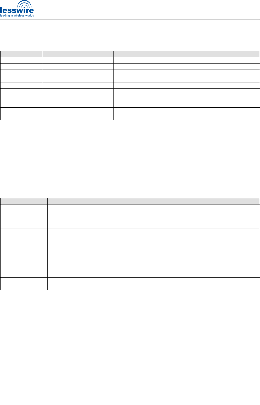
Block Diagrams
WiBear11n-SF1
WiBear11n-SF2
802.11b/g/n MAC/BB/RADIO
BLUETOOTH 3.0+HS
2.4 GHz
RF FRONT
END
2.5GHz WLAN TX
2.5GHz WLAN/BT RX
BT TX
WLAN &
BT ANT
VIO
1.8V
3.3V
2.5GHz
2.4GHz
BPF
WiBear11n-SF1
EEPROM
38.4
MHz
Crystal
SDIO
RESETn
PDn
SLEEP
CLOCK
GPIOs
802.11b/g/n MAC/BB/RADIO
BLUETOOTH 3.0+HS
EEPROM
SDIO
38.4
MHz
Crystal
2.4 GHz
RF FRONT
END
2.5GHz WLAN TX
2.5GHz WLAN RX
BT TX/RX
WLAN ANT
RESETn
PDn
VIO
1.8V
3.3V
2.5GHz
2.4GHz
BPF
SLEEP
CLOCK
WiBear11n-SF2
BT ANT
2.4GHz
BPF
GPIOs
Figure 2: Block diagram of WiBear11n-SF1
Figure 3: Block diagram of WiBear11n-SF2
WiBear11n Data Sheet
Version 1.18
Copyright © 2013 lesswire AG
www.lesswire.com
Page 5 of 20
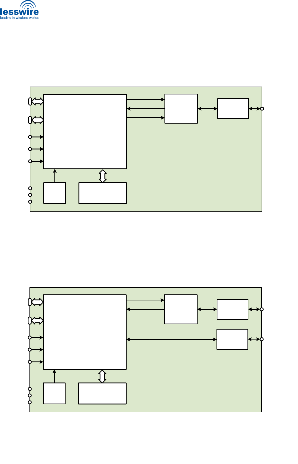
WiBear11n-DF1
WiBear11n-DF2
802.11a/b/g/n MAC/BB/RADIO
BLUETOOTH 3.0+HS
2.4 GHz
RF FRONT
END
2.5GHz WLAN TX
2.5GHz WLAN/BT RX
BT TX
WLAN &
BT ANT
VIO
1.8V
3.3V
5GHz WLAN TX
5GHz WLAN RX
5 GHz
RF FRONT
END
5GHz BPF
&
DIPLEXER
5GHz
2.5GHz
2.4GHz
BPF
WiBear11n-DF1
EEPROM
SDIO
38.4
MHz
Crystal
RESETn
PDn
SLEEP
CLOCK
GPIOs
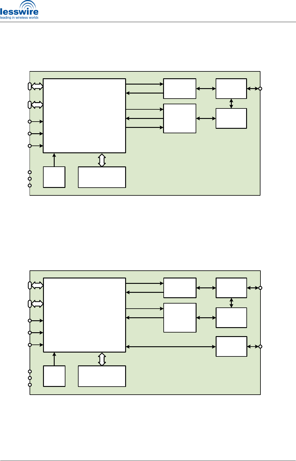
802.11a/b/g/n MAC/BB/RADIO
BLUETOOTH 3.0+HS
2.4 GHz
RF FRONT
END
2.5GHz WLAN TX
2.5GHz WLAN RX
BT TX/RX
WLAN ANT
VIO
1.8V
3.3V
5GHz WLAN TX
5GHz WLAN RX
5 GHz
RF FRONT
END
5GHz BPF
&
DIPLEXER
5GHz
2.5GHz
2.4GHz
BPF
WiBear11n-DF2
BT ANT
2.4GHz
BPF
EEPROM
SDIO
38.4
MHz
Crystal
RESETn
PDn
SLEEP
CLOCK
GPIOs
Figure 4: Block diagram of WiBear11n-DF1
Figure 5: Block diagram of WiBear11n-DF2
WiBear11n Data Sheet
Version 1.18
Copyright © 2013 lesswire AG
www.lesswire.com
Page 6 of 20
Pin Description
Table 3: Pin description
Pin
No.
Pin Name Pin Type Description
1 GND Ground Ground
2 LED_0 I/O LED output (GPIO_1 of Radio/Baseband processor), WLAN activity
1
3 LED_1 I/O LED output (GPIO_17 of Radio/Baseband processor), Bluetooth activity
1
4 3V3 Power 3.3V Power supply (3.0V...3.6V)
5 VIO Power VIO Supply (1.8V or 3.3V)
6 1V8 Power 1.8V Supply (1.7V...1.9V)
7 GND Ground Ground
8 GND Ground Ground
9 PDn I Full power down (active low), has internal pull-up to VIO pin
10 RESETn I Reset (active low), has weak internal pull-up to VIO pin
11 SD_D2 I/O SDIO Data line bit [2]
12 SD_D3 I/O SDIO Data line bit [3]
13 SD_CMD I/O SDIO Command
14 SD_CLK I SDIO Clock input
15 SD_D0 I/O SDIO Data line bit [0]
16 SD_D1 I/O SDIO Data line bit [1]
17 GND Ground Ground
18 GND Ground Ground
19 SLEEP_CLK I Clock input for external sleep clock source (32.768kHz)
2
20 CFG I/O Configuration pin
3
21 PCM_SYNC I/O GPIO_14 of Radio/Baseband processor, output if master, input if slave
22 PCM_CLK I/O GPIO_13 of Radio/Baseband processor, output if master, input if slave
23 PCM_DOUT O GPIO_12 of Radio/Baseband processor, output
24 PCM_DIN I GPIO_11 of Radio/Baseband processor, input
25 GND Ground Ground
GND
LED_0
LED_1
3V3
VIO
1V8
GND
GND
1
2
3
4
5
6
7
8
PDn
RESETn
SD_D2
SD_D3
SD_CMD
SD_CLK
SD_D0
SD_D1
14
15
16
10
11
12
13
9
24
23
22
21
20
19
18
17
GND
GND
SLEEP_CLK
CFG
PCM_SYNC
PCM_CLK
PCM_DOUT
PCM_DIN
30
29
28
27
26
25
GND
ANT2
GND
GND
ANT1
GND
Figure 6: Module pinout

WiBear11n Data Sheet
Version 1.18
Copyright © 2013 lesswire AG
www.lesswire.com
Page 7 of 20
26 ANT2 I/O, RF Bluetooth antenna for WiBear11n-SF2/-DF2 module, at WiBear-SF1/-DF1
not connected
27 GND Ground Ground
28 GND Ground Ground
29 ANT1 I/O, RF WLAN + Bluetooth antenna for WiBear11n-SF1/-DF1 module, WLAN only
antenna for WiBear11n-SF2/-DF2 module
30 GND Ground Ground
NOTES:
1
Possible to use as a LED output depend on firmware (driver) version. Regardless of the I/O supply
(1.8V or 3.3V), the supply to the actual board LED always need to use 3.3V on the other end of the
LED and works as open drain circuitry in that case. LED current limiting resistor should be used.
Maximum sink to the ground current - 10 mA.
2
Should be provided from external source in case of power save operation modes necessity. Not
required for full power mode and for automotive use (firmware & driver version 14.44). Mandatory
for all other releases with sleep mode support. Sleep clock signal requirements: frequency
32.768kHz ±250ppm, low level from 0 to 0.25V, high level from 0.8 to 2.0V, duty cycle 20-80%,
slew rate less than 100nS (10-90%).
3
Leave it unconnected when 32.768KHz Sleep Clock provided, pull down by 47K resistor for Sleep
Clock less operation.
WiBear11n Data Sheet
Version 1.18
Copyright © 2013 lesswire AG
www.lesswire.com
Page 8 of 20
Electrical Specifications
Absolute Maximum Ratings
Table 4: Absolute maximum ratings
Name Parameter Min Max Units
3V3 Power supply voltage 3.3V -0.3 3.6 V
1V8 Power supply voltage 1.8V -0.3 2.0 V
VIO I/O supply voltage 1.8V/2.6/3.3V -0.3 3.6 V
T
STORAGE
Storage temperature -40 +85 ºC
Operating Conditions
Table 5: Operating conditions
Name Parameter Min Typ Max Units
3V3 Power supply voltage 3.3V 3.1 3.3 3.6 V
1V8 Power supply voltage 1.8V 1.74 1.8 1.89 V
1.62 1.8 1.98 V VIO I/O supply voltage 1.8V/3.3V
3.0 3.3 3.6 V
T
A
Ambient operating temperature -40 - +85 ºC
Ripple
Noise
Peak-to-peak voltage ripple on 3V3 and 1V8 supply
lines.
- - 10 mV
Digital Pad Ratings
Table 6: Digital pad ratings
Name Parameter Mode
1
Min Max Units
1.8V 0.8*1V8 1V8+0.3 V V
IH
Input high voltage
3.3V 0.7*3V3 3V3+0.3 V
1.8V -0.3 0.3*1V8 V V
IL
Input low voltage
3.3V -0.3 0.3*3V3 V
1.8V 150 - mV V
HYS
Input hysteresis
3.3V 200 - mV
1.8V 1V8-0.4 - V V
OH
Output high voltage
3.3V 3V3-0.4 - V
1.8V - 0.4 V V
OH
Output low voltage
3.3V - 0.4 V
Note:
1
IO voltage, see table above for possible IO voltage range.
Current Consumption
Table 7: Current consumption
Current, mA
1
Operation mode 1.8V VIO
2
3.3V
2.4GHz 145 10 0.1
RX 5GHz 150 10 14
+18dBm 140 10 200
+15dBm 140 10 170
+12dBm 140 10 145
2.4GHz
+6dBm 140 10 120
+15dBm 150 10 200
+12dBm 150 10 170
TX
5GHz
+6dBm 150 10 150
Notes:
1
Peak values shown, average current for full operation mode (not a power save mode) strongly
depend on RX/TX time ratio and remain in range between peak values of RX and TX.
2
VIO current shown for 3.3V I/O voltage.
WiBear11n Data Sheet
Version 1.18
Copyright © 2013 lesswire AG
www.lesswire.com
Page 9 of 20
Radio Specifications
WLAN
Module supports dual-band 802.11b/g/n and 802.11a/n operation in both 2.4 GHz and 5 GHz radio bands,
respectively. Therefore the module is designed to operate in only one frequency band at time.
Table 8: WLAN radio specifications
Parameter Operation mode Specification
802.11b/g/n 2.400 – 2.500 GHz
RF Frequency Range 802.11a/n 4.900 – 5.825 GHz
802.11b CCK and DSSS
Modulation 802.11a/g/n OFDM
802.11b 1, 2, 5.5, 11 Mbps
802.11a/g 6, 9, 12, 18, 24, 36, 48, 54 Mbps
Supported Data Rates
802.11n MCS0 - MCS7
Supported Bandwidth 802.11n 20, 40 MHz
Supported Guard Interval 802.11n 400, 800 mS
802.11b 18 dBm ± 1 dB
Maximum Transmit Power 802.11a/g/n 15 dBm ± 1 dB
1 Mbps -96 dBm ± 1 dB
802.11b 11 Mbps -87 dBm ± 1 dB
6 Mbps -89 dBm ± 1 dB
802.11g 54 Mbps -71 dBm ± 1 dB
MCS0 -88 dBm ± 1 dB
20 MHz MCS7 -69 dBm ± 1 dB
MCS0 -85 dBm ± 1 dB
2.4 GHz
802.11n
40 MHz MCS7 -66 dBm ± 1 dB
6 Mbps -92 dBm ± 1 dB
802.11a 54 Mbps -75 dBm ± 1 dB
MCS0 -91 dBm ± 1 dB
20 MHz MCS7 -72 dBm ± 1 dB
MCS0 -89 dBm ± 1 dB
Receiver Sensitivity
5 GHz
802.11n
40 MHz MCS7 -69 dBm ± 1 dB
Table 9: 2.4 GHz Band Supported Channels, 20MHz bandwidth
Channel Frequency,
GHz Channel Frequency,
GHz Channel Frequency,
GHz
1 2.412 6 2.437 11 2.462
2 2.417 7 2.442 12 2.467
3 2.422 8 2.447 13 2.472
4 2.427 9 2.452 14
1
2.484
5 2.432 10 2.457
Note:
1
Channel 14 supported at 802.11b mode only
Table 10: 2.4 GHz Band Supported Channels, 40MHz bandwidth
Channel Frequency,
GHz Channel Frequency,
GHz Channel Frequency,
GHz
1 5 2.422 4 8 2.437 7 11 2.452
2 6 2.427 5 9 2.442
3 7 2.432 6 10 2.447
WiBear11n Data Sheet
Version 1.18
Copyright © 2013 lesswire AG
www.lesswire.com
Page 10 of 20
Table 11: 5 GHz Band Supported Channels, 20MHz bandwidth
Channel Frequency,
GHz Channel Frequency,
GHz Channel Frequency,
GHz
36 5.180 100 5.500 132 5.660
40 5.200 104 5.520 136 5.680
44 5.220 108 5.540 140 5.700
48 5.240 112 5.560 149 5.745
52 5.260 116 5.580 153 5.765
56 5.280 120 5.600 157 5.785
60 5.300 124 5.620 161 5.805
64 5.320 128 5.640 165 5.825
Table 12: 5 GHz Band Supported Channels, 40MHz bandwidth
Channel Frequency,
GHz Channel Frequency,
GHz Channel Frequency,
GHz
36 40 5.190 100 104 5.510 132 136 5.670
44 48 5.230 108 112 5.550 149 153 5.755
52 56 5.270 116 120 5.590 157 161 5.795
60 64 5.310 124 128 5.630
Bluetooth
Table 13: Bluetooth Radio specifications
Parameter Specification
RF Frequency Range 2.400 – 2.4835 GHz
Supported Modes BT 2.1 EDR, BT3.0 HS
Number of channels 79
Modulation 1 Mbps: GFSK (BDR)
2 Mbps: π/4 DQPSK (EDR)
3 Mbps: 8DQPSK (EDR)
Transmit Power +8 dBm ± 1.5 dB
Receiver Sensitivity BDR: -90 dBm ± 1.5 dB
EDR: -87 dBm ± 1.5 dB
WiBear11n Data Sheet
Version 1.18
Copyright © 2013 lesswire AG
www.lesswire.com
Page 11 of 20
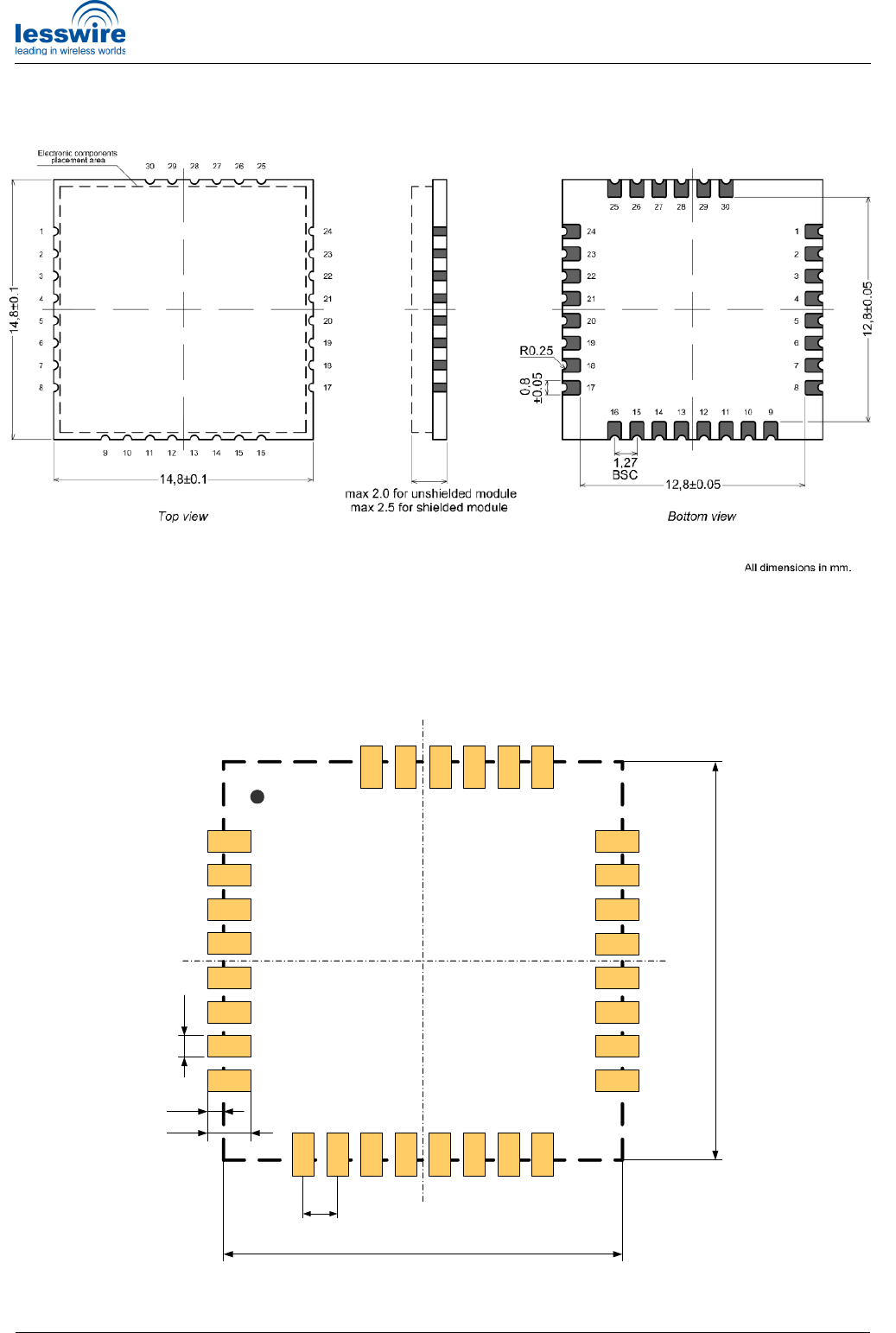
Physical Dimensions
Note: The tolerances +/- 0.1 mm may be exceeded in the corners of the PCB due to the cutting process. In
worst case, the outer dimensions could reach 15.1 mm.
Recommended Footprint
Figure 7: Physical dimensions
Figure 8: Recommended footprint
14
2
15 1610 11 12 139
3
4
5
6
7
8
1
23
22
21
20
19
18
17
24
26 25
1.6
0.6
0.8
14.8
Pitch=1.27
14.8
27282930
WiBear11n Data Sheet
Version 1.18
Copyright © 2013 lesswire AG
www.lesswire.com
Page 12 of 20
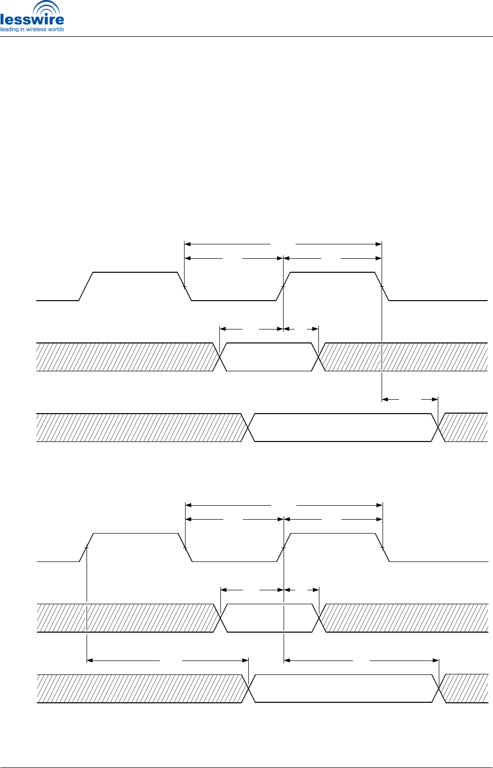
Host Interfaces
SDIO Interface
WiBear11n module supports a SDIO device interface that conforms to the industry standard SDIO Full-Speed
specification and allows a host controller using the SDIO bus protocol to access the WLAN and Bluetooth
functions. The module also supports High Speed mode as defined in the SDIO 1.2 specification.
The module's SDIO host interface pins are powered from the VIO voltage supply.
A module acts as the device on the SDIO bus. The SDIO interface supports SDIO modes at the full clock range
of 0 to 50 MHz which allows a maximum throughput of 200Mbps.
Clock
T
WH
f
PP
Input
Output
T
WL
T
ISU
T
IH
T
ODLY
T
OH
Clock
T
WH
f
PP
Input
Output
T
WL
T
ISU
T
IH
T
ODLY
Figure 9: SDIO Protocol Timing Diagram
Figure 10: SDIO Protocol Timing Diagram at High Speed Mode

WiBear11n Data Sheet
Version 1.18
Copyright © 2013 lesswire AG
www.lesswire.com
Page 13 of 20
Table 14: SDIO Host Interface Timing Data
Symbol
Parameter Condition Min Typ Max Units
Normal 0 - 25 MHz f
PP
Clock Frequency
High Speed 0 - 50 MHz
Normal 10 - - ns T
WL
Clock Low Time
High Speed 7 - - ns
Normal 10 - - ns T
WH
Clock High Time
High Speed 7 - - ns
Normal 5 - - ns T
ISU
Input Setup Time
High Speed 6 - - ns
Normal 5 - - ns T
IH
Input Hold Time
High Speed 2 - - ns
Normal - - 14 ns T
ODLY
Output Delay Time
High Speed - - 14 ns
T
OH
Output Hold Time High Speed 2.5 - - ns
WiBear11n Data Sheet
Version 1.18
Copyright © 2013 lesswire AG
www.lesswire.com
Page 14 of 20
Reference Design
Overview
Reference design shows how to connect a WiBear11n module to the host controller. WLAN and Bluetooth
(BT3.0 HS + EDR) may be connected to the host simultaneously over the SDIO bus. The layout is equipped
with the possibility to either use an onboard antenna or an external antenna connected via coaxial connector by
means of setting of jumper R7 or R8. Host interface voltage can also be changed by jumper J6. The ready-
made reference design is available as WiBear11n Evaluation Kit from Lesswire AG.
Schematic Diagram
C1
100nF
D3
Blue
D1
Green
D2
Orange
J2
IN
1
EN
3
GND
2NC 4
OUT 5
U2
MCP1824T-1802E
DAT2 9
DAT3 1
CMD 2
GND 3
VDD 4
CLK 5
GND 6
DAT0 7
DAT1 8
SDIO
1 2
3 4
5 6
7 8
9 10
12
14
11
13
J1
R1
360 R2
620
C2
10uF
3V3
R3
3.6k
3V3
MAIN
J3
AUX
LED_1LED_0
3V3
1V83V3
RESET
SD_D2
SD_D3
CMD
CLK
SD_D0
SD_D1
3V3
3V3
SD_D2
SD_D3
CMD
CLK
SD_D0
SD_D1
SD_D2
SD_D3
CMD
CLK
SD_D0
SD_D1
SDIO
Assembly
Option Description
WLAN and Bluetooth at the same antenna terminal (U1:Pin 44)
WLAN and Bluetooth at the different antenna terminals
1
2
J3
"Supply" "WLAN" "BT"
DNP
+
R7
0
U1
WiBear11n-DF1
(U1:Pin 29 and U1:Pin 26 correspondingly) for uAP functionality
WiBear11n-SF1
RESET
WiBear11n-DF2
WiBear11n-SF2
SLP_CLK
SLP_CLK
C3
10uF
RESET 1
MR
3
GND 2
CT
4
SENSE
5VDD 6
U3
TPS3808G30
LED_0
LED_1
1V8
J6
J4
R6
47K
CFG
CFG
A1
Dual Band
Antenna
J5
R4
10K
C4
100nF
3V3 VIO
R5
10K
RESET
1V8
3V3
VIO
J7
J8
R8
DNP
20mS Reset Pulse
C7
2.2pF
L1
6.8nH L2
12nH
EN
1GND 2
OUT 3
VCC
4
Y1
32.768kHz
C6
100nF
10mS Start Up Time
SD_D2
11
SD_D3
12
SD_CMD
13
SD_CLK
14
SD_D0
15
SD_D1
16
RESET
10 PD
9
3V3
4
VIO
5
1V8
6
GND 1
GND 7
SLP_CLK
19
LED_1
3
PCM_DOUT
23 PCM_CLK
22
GND 8
LED_0
2
CFG
20
PCM_SYNC
21
GND 17
ANT2 26
GND 18
PCM_DIN
24
ANT1 29
GND 25
GND 27
GND 28
GND 30
U1
WiBear11n
C5
DNP
Antenna matching components (L1, C7, L2)
values depend on antenna type,
layout, PCB material and PCB thickness
1
2
3
1
2
3
Figure 11: Evaluation Kit outlook
Figure 12: Evaluation kit schematic diagram
WiBear11n Data Sheet
Version 1.18
Copyright © 2013 lesswire AG
www.lesswire.com
Page 15 of 20
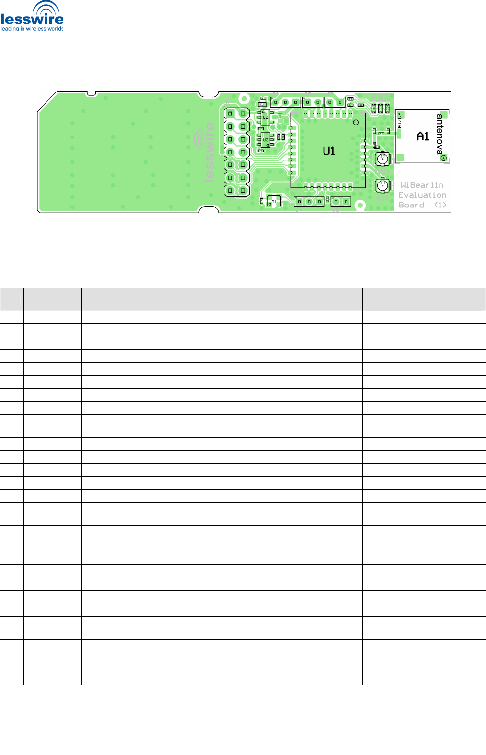
Assembly diagram
Bill of Materials
Table 15: Bill of materials
Qty
Designator
Part Description Manufacturer Part
Number
1
A1 Antenna CHIP 2.45 & 5 GHz, 10.4x10.4x0.8mm Antenova: A10194
3
C1, C4, C6 CAP, CER, 100nF, 10%, X7R, 16V, SMD 0402 Generic Components
2
C2, C3 CAP, CER, 10uF, 20%, X5R, 6.3V, SMD 0603 Generic Components
1
C5 DNP Generic Components
1
C7 CAP, CER, 2.2pF, +/-0.25pF, C0G, 50V, SMD 0402 Generic Components
1
D1 LED, Green, SMD 0603 Avago: HSMG-C190
1
D2 LED, Orange, SMD 0603 Avago: HSMD-C190
1
D3 LED, Blue, SMD 0603 Avago: HSMR-C190
1
J1
Pin Header, Double Row, 2.54mm pitch, Straight, 2x7 Way,
Through Hole Generic Components
2
J2, J3 Coaxial Connector, 0 - 6GHz, SMD Hirose: U.FL-R-SMT
2
J4, J6 Pin Header, Pitch 2.0mm, 1x3 Way, Through Hole Samtec: TMM-103-01-G-S
3
J5, J7, J8 Pin Header, Pitch 2.0mm, 1x2 Way, Through Hole Samtec: TMM-102-01-G-S
1
L1 IND, Multilayer Ceramic, 6.8nH, +/-5%, 300mA, SMD 0402 Generic Components
1
L2 IND, Multilayer Ceramic, 12nH, +/-5%, 300mA, SMD 0402 Generic Components
1
PCB PCB, Dual side, 82x24x1.5mm, Rev.1A
Lesswire AG:
WiBear11n_EK_R1
1
R1 RES, 360 Ohm, 5%, 1/16W, SMD 0402 Generic Components
1
R2 RES, 620 Ohm, 5%, 1/16W, SMD 0402 Generic Components
1
R3 RES, 3.6k, 5%, 1/16W, SMD 0402 Generic Components
2
R4, R5 RES, 10k, 5%, 1/16W, SMD 0402 Generic Components
1
R6 RES, 47K, 5%, 1/16W, SMD 0402 Generic Components
2
R7, R8 RES, 0 Ohm, 1/16W, SMD 0402 Generic Components
1
U1 WLAN 802.11a/b/g/n and Bluetooth Module, 14.8x14.8x2.5mm
Lesswire AG: WiBear11n
1
U2 CMOS LDO Voltage Regulator 1.8V 300mA, SOT23-5
Microchip: MCP1824T-
1802E/OT
1
U3
Voltage supervisor, programmable reset time, threshold
voltage 2.79V, SOT23-6
Texas Instruments:
TPS3808G30
1
Y1
Quartz Oscillator, 32.768kHz, 1.8V, +/-50ppm, -40...+85C,
SMD 3.2x2.5x1.0mm Pericom: KK3270049
Figure 13: Evaluation kit assembly diagram
WiBear11n Data Sheet
Version 1.18
Copyright © 2013 lesswire AG
www.lesswire.com
Page 16 of 20
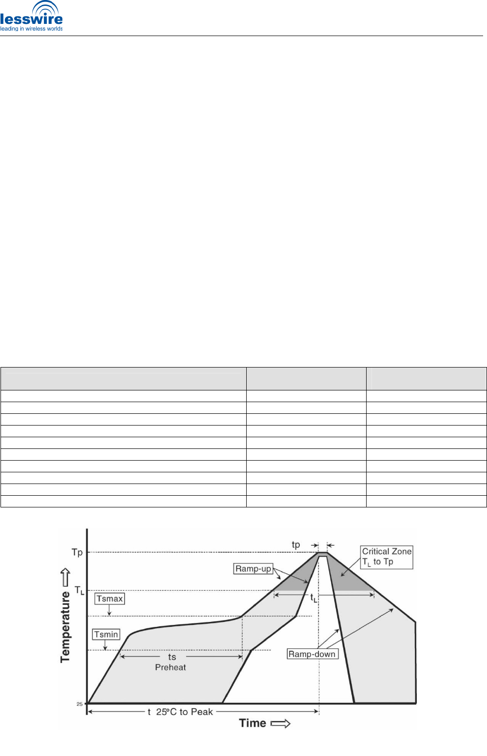
Mounting process
The WiBear11n is a surface mount module supplied on a 6-layer FR4-type PCB with gold plated connection
pads and produced in a lead-free process with a lead-free soldering paste. The warpage of the PCB is max.
0,75% according to IPC-A-610E. The thickness of solder resist on the host PCB top side and the WiBear11n
bottom side must be considered for the soldering process.
Modules rated at moisture sensitivity level 3. See moisture sensitive warning label on each shipping bag for
detailed information. After opening the dry pack, modules must be mounted within 168 hours in factory
conditions of maximum 30°C/60%RH or must be stored at less than 10%RH. Modules require baking if the
humidity indicator card shows more than 10% when read at 23±5°C or if the conditions mentioned above are
not met. Please refer to J-STD-033B standard for bake procedure.
Module is compatible with industrial reflow profile for RoHS/Pb-free solders, Sn96.5/Ag3.0/Cu0.5 solder is a
right choice. Use of "No Clean" soldering paste is strongly recommended, cleaning the populated modules is
strongly discouraged - residuals under the module cannot be easily removed with any cleaning process.
Cleaning with water can lead to capillary effects where water is absorbed into the gap between the host board
and module. The combination of soldering flux residuals and encapsulated water could lead to short circuits
between neighboring pads.
Only a single reflow soldering process is permitted for host boards with WiBear11n modules.
The reflow profile used is dependent on the thermal mass of the entire populated PCB, heat transfer efficiency
of the oven and particular type of solder paste used. Since the profile used is process and layout dependent,
the optimum profile should be studied case by case. Recommendations below should be taken as a starting
point guide. In case of basic information necessity please refer to J-STD-020C standard.
Table 16: Recommended reflow profile
Profile feature Sn-Pb eutectic
(Sn63/Pb37)
RoHS/Pb-free
(Sn96.5/Ag3.0/Cu0.5)
Ramp up rate (T
SMAX
to T
P
) 3°C/sec max 3°C/sec max
Minimum soak temperature (T
SMIN
) 100°C 150°C
Maximum soak temperature (T
SMAX
) 150°C 200°C
Soak time (ts) 60 - 120 sec 60 - 180 sec
Liquidus temperature (T
L
) 183°C 217°C
Time above T
L
(t
L
) 60 - 150 sec 60 - 150 sec
Peak temperature (T
P
) 215 - 225°C 235 - 245°C
Time within +0 / -5°C of actual T
P
(tp) 10 - 30 sec 20 - 40 sec
Ramp down rate 6°C/sec max 6°C/sec max
Time from 25°C to T
P
6 min max 8 min max
Note: lowest value of T
P
and slower ramp down rate (2 - 3°C/sec) is preferred.
Figure 14: Reflow profile

WiBear11n Data Sheet
Version 1.18
Copyright © 2013 lesswire AG
www.lesswire.com
Page 17 of 20
Installation and Regulatory Information
General
The purpose of this guide is to explain how to integrate the WiBear11n module into the end product. The
module has to be installed and used in accordance with the technical instructions provided by the
manufacturer. The module may only be implemented in the configuration that was authorized. Note that any
modifications of this equipment not expressly approved by the manufacturer could void the user’s authority to
operate the equipment.
European Union Regulatory Compliance
The WiBear11n module has been tested and complies with the regulatory standards EN 300 328 and EN 301
489-1/-17. We declare that the human exposure of this module is below the SAR limits specified in the EU
recommendations 1999/519/EC.
IMPORTANT: The ‘CE’ marking must be affixed to a visible location on the OEM product, where this module is
installed in, and has to be labeled in accordance to R&TTE Directive 1999/5/EC.
FCC Compliance
This device complies with Part 15 of the FCC Rules
1
. Operation is subject to the following two conditions:
(1) This device may not cause harmful interference, and
(2) this device must accept any interference received, including interference that may cause undesired
operation.
Not authorized modification could void authority to use this equipment.
The internal / external antenna(s) used for this module must provide a separation distance of at least 20 cm
from all persons and must not be co-located or operating in conjunction with any other antenna or transmitter.
NOTE: The outside of final product that contain a WiBear11n module must display in a user accessible area a
label referring to the enclosed module. This exterior label can use wording such as the following: “Contains
Transmitter Module FCC ID: PV7-WIBEAR11N-SF1”
2
or “Contains FCC ID: PV7-WIBEAR11N-SF1”.
IMPORTANT: The approval type for the WiBear11n variants is a limited modular approval due to the absence
of a shielding. This requires any manufacturer of original equipment containing the WiBear11n module to ask
for an approval of their design by the manufacturer of the WiBear11n module.
IC Compliance
This device complies with Industry Canada RSS-210 (Rev. 8). Operation is subject to the following two
conditions:
(1) this device may not cause interference, and
(2) this device must accept any interference, including interference that may cause undesired operation of the
device.
Le présent appareil est conforme aux CNR d'Industrie Canada applicables aux appareils radio exempts de
licence. L'exploitation est autorisée aux deux conditions suivantes:
(1) l'appareil ne doit pas produire de brouillage, et
(2) l'utilisateur de l'appareil doit accepter tout brouillage radioélectrique subi, même si le brouillage est
susceptible d'en compromettre le fonctionnement.
The installer of this radio equipment must ensure that the antenna is located or pointed such that it does not
emit RF field in excess of Health Canada limits for the general population; consult Safety Code 6, obtainable
from Health Canada.
Not authorized modification could void authority to use this equipment.
1
Limited modular approval has been applied for the module variant WiBear11n-SF1, the certification process for the other
module variants is ongoing.
2
FCC and IC IDs for the WiBear11n module variants are shown in Table 19. Select the applicable ID.
WiBear11n Data Sheet
Version 1.18
Copyright © 2013 lesswire AG
www.lesswire.com
Page 18 of 20
The internal / external antenna(s) used for this module must provide a separation distance of at least 20 cm
from all persons and must not be co-located or operating in conjunction with any other antenna or transmitter.
NOTE: The outside of final product that contain a WiBear11n module must display in a user accessible area a
label referring to the enclosed module. This exterior label can use wording such as the following: “Contains
Transmitter Module IC ID: 7738A-WB11NSF1”
2
or “Contains IC ID: 7738A-WB11NSF1”.
IMPORTANT: The approval type for the WiBear11n variants is a limited modular approval due to the absence
of a shielding. Due to Industry Canada Modular Approval Requirements (Source: RSS-Gen / Issue 3 / Dec.
2010) any application which includes the WiBear11n module must be approved by the module manufacturer
(lesswire AG). The application manufacturer must provide design data for the review procedure.
Approved Antennas List
For Bluetooth and WLAN operation in the 2.4 GHz band, the module has been tested and approved for use
with the antenna listed in the table below.
Table 17: Approved antennas list, single-band operation
Model Name Manufacturer and description Gain [dBi]
2450AT45A100 Johanson Technology, Chip antenna, 2400 – 2500 MHz 3.0 (peak)
For Bluetooth, WLAN operation in the 2.4 GHz band, and WLAN operation in the 5 GHz band, the module has
been tested and approved for use with the antenna listed in the table below.
Table 18: Approved antennas list, dual-band operation
Model Name Manufacturer and description Gain [dBi]
A10194 Antenova, dual-band SMD antenna, 2.4 – 2.5 GHz and
4.9 – 5.9 GHz
1.8 (peak)
The module may be integrated with other antennas which the OEM installer must authorize with respective
regulatory agencies and after approval of the module manufacturer.
FCC and IC IDs
Table 19: FCC and IC IDs for WiBear11n module variants
Model Model number FCC ID IC ID
WiBear11n-SF1 AN00J93170 PV7-WIBEAR11N-SF1 7738A-WB11NSF1
WiBear11n-SF2 AN00J93174 PV7-WIBEAR11N-SF2 7738A-WB11NSF2
WiBear11n-DF1 AN00J93172 PV7-WIBEAR11N-DF1 7738A-WB11NDF1
WiBear11n-DF2 AN00J93176 PV7-WIBEAR11N-DF2 7738A-WB11NDF2
Label
Due to the small module size, the FCC and IC IDs cannot be displayed on the label. The corresponding FCC
and IC IDs for the module variants are shown in the table above.
WiBear11n Data Sheet
Version 1.18
Copyright © 2013 lesswire AG
www.lesswire.com
Page 19 of 20
Label drawing: Label location:
Figure 15: Label and label location
WiBear11n Data Sheet
Version 1.18
Copyright © 2013 lesswire AG
www.lesswire.com
Page 20 of 20
Revision History
Table 20: Revision history
Date Version
Author Description
20-Jun-2012 1.00 Igor Shevchenko Preliminary release
22-Jun-2012 1.01
Igor Shevchenko
Andras Varadi
Andreas Beierer
Some minor mistakes fixed
16-Jul-2012 1.02 Igor Shevchenko PCM interface description added, Supported channels
presented in region independent form.
01-Oct-2012 1.03 Igor Shevchenko Minor mistakes fixed, Evaluation Kit information added
05-Dec-2012 1.04 Daniel Dietterle Updated order codes for latest hardware revision C
11-Jan-2013 1.05 Daniel Dietterle Added installation and regulatory information
16-Jan-2013 1.06 Daniel Dietterle Added label information and table with FCC/IC IDs
18-Jan-2013 1.07 Igor Shevchenko Added Wi-Fi Direct mode support
18-Jan-2013 1.08 Igor Shevchenko Requirements (Note 2) for Sleep Mode updated
22-Jan-2013 1.09 Daniel Dietterle Added paragraph on IC compliance
06-Feb-2013 1.10 Daniel Dietterle Added paragraph on IC compliance in French language
22-Feb-2013 1.11 Igor Shevchenko Dimension drawing improved (tolerances added)
25-Feb-2013 1.12 Daniel Dietterle FCC ID's and IC ID's with cross-reference to model numbers
28-Mar-2013 1.13 Daniel Dietterle Added: RoHS compliance; mounting process (warpage);
custom tariff numbers; IMDS number
07-May-2013 1.14 Daniel Dietterle
Electrical specification updated: minimum supply voltage and
ripple noise, digital pad ratings corrected
Physical dimensions: Contour tolerances in corners of the PCB
added
14-May-2013 1.15 Daniel Dietterle Added order information for tape&reel packing
15-May-2013 1.16 Daniel Dietterle Corrected ordering information for variants DF1 and SF2 (T&R)
21-May-2013 1.17 Daniel Dietterle Release, no changes.
19-Dec-2013 1.18 Daniel Dietterle Approved antenna list extended