u blox WIBEAR11N-DF1 WLAN & Bluetooth Module User Manual WiBear11n DS
u-blox AG WLAN & Bluetooth Module WiBear11n DS
UserManual.wiki
>
u blox
>
WIBEAR11N-DF1 User Manual
>
user manual
Contents
1.
user manual
2.
User Manual
3.
ELLA-W1_Antenna TraceDesigns_(UBX-16016269)
user manual
Navigation menu
Upload a User Manual
Namespaces
Wiki Guide
HTML
PDF
Info
Views
User Manual
Discussion / Help
Navigation
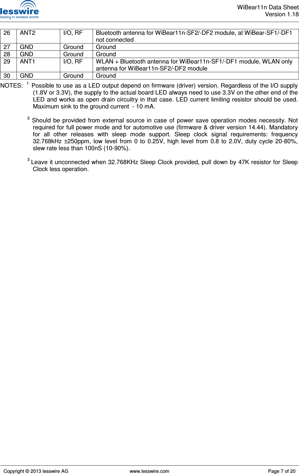
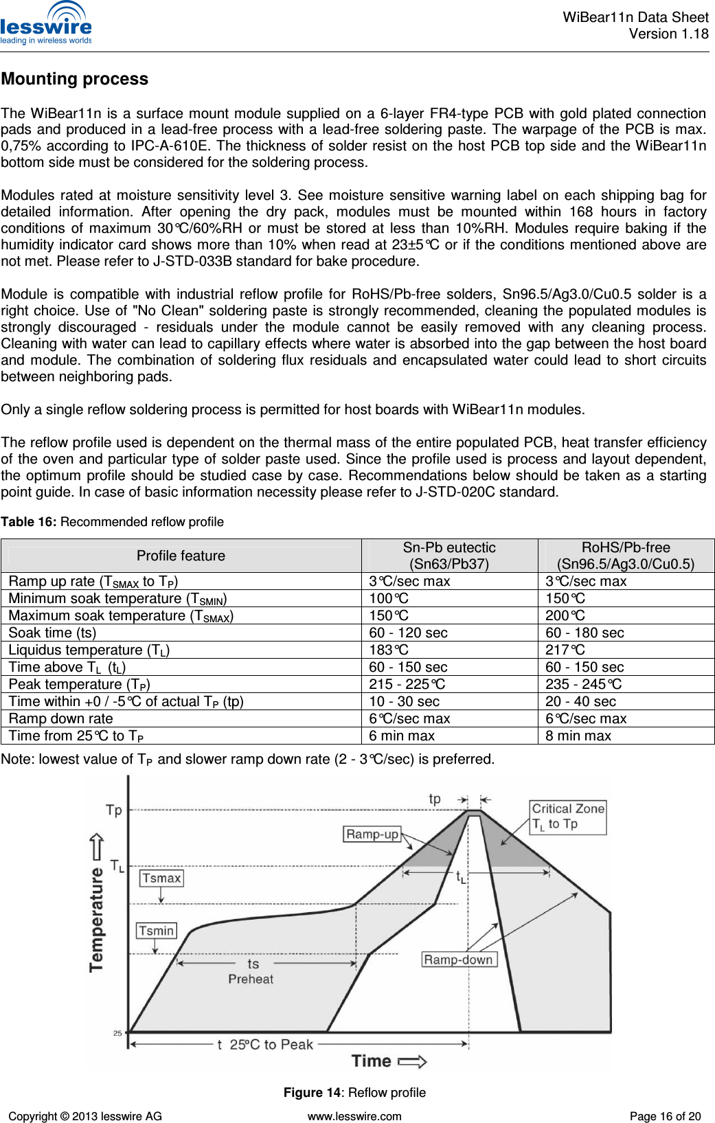
![WiBear11n Data SheetVersion 1.18 Copyright © 2013 lesswire AG www.lesswire.com Page 6 of 20 Pin Description Table 3: Pin description Pin No. Pin Name Pin Type Description 1 GND Ground Ground 2 LED_0 I/O LED output (GPIO_1 of Radio/Baseband processor), WLAN activity 1 3 LED_1 I/O LED output (GPIO_17 of Radio/Baseband processor), Bluetooth activity 1 4 3V3 Power 3.3V Power supply (3.0V...3.6V) 5 VIO Power VIO Supply (1.8V or 3.3V) 6 1V8 Power 1.8V Supply (1.7V...1.9V) 7 GND Ground Ground 8 GND Ground Ground 9 PDn I Full power down (active low), has internal pull-up to VIO pin 10 RESETn I Reset (active low), has weak internal pull-up to VIO pin 11 SD_D2 I/O SDIO Data line bit [2] 12 SD_D3 I/O SDIO Data line bit [3] 13 SD_CMD I/O SDIO Command 14 SD_CLK I SDIO Clock input 15 SD_D0 I/O SDIO Data line bit [0] 16 SD_D1 I/O SDIO Data line bit [1] 17 GND Ground Ground 18 GND Ground Ground 19 SLEEP_CLK I Clock input for external sleep clock source (32.768kHz) 2 20 CFG I/O Configuration pin 3 21 PCM_SYNC I/O GPIO_14 of Radio/Baseband processor, output if master, input if slave 22 PCM_CLK I/O GPIO_13 of Radio/Baseband processor, output if master, input if slave 23 PCM_DOUT O GPIO_12 of Radio/Baseband processor, output 24 PCM_DIN I GPIO_11 of Radio/Baseband processor, input 25 GND Ground Ground GNDLED_0LED_13V3VIO1V8GNDGND12345678PDnRESETnSD_D2SD_D3SD_CMDSD_CLKSD_D0SD_D11415161011121392423222120191817GNDGNDSLEEP_CLKCFGPCM_SYNCPCM_CLKPCM_DOUTPCM_DIN302928272625GNDANT2GNDGNDANT1GNDFigure 6: Module pinout](https://usermanual.wiki/u-blox/WIBEAR11N-DF1.user-manual/User-Guide-2237875-Page-6.png)
![WiBear11n Data SheetVersion 1.18 Copyright © 2013 lesswire AG www.lesswire.com Page 18 of 20 The internal / external antenna(s) used for this module must provide a separation distance of at least 20 cm from all persons and must not be co-located or operating in conjunction with any other antenna or transmitter. NOTE: The outside of final product that contain a WiBear11n module must display in a user accessible area a label referring to the enclosed module. This exterior label can use wording such as the following: “Contains Transmitter Module IC ID: 7738A-WB11NSF1”2 or “Contains IC ID: 7738A-WB11NSF1”. IMPORTANT: The approval type for the WiBear11n variants is a limited modular approval due to the absence of a shielding. Due to Industry Canada Modular Approval Requirements (Source: RSS-Gen / Issue 3 / Dec. 2010) any application which includes the WiBear11n module must be approved by the module manufacturer (lesswire AG). The application manufacturer must provide design data for the review procedure. Approved Antennas List For Bluetooth and WLAN operation in the 2.4 GHz band, the module has been tested and approved for use with the antenna listed in the table below. Table 17: Approved antennas list, single-band operation Model Name Manufacturer and description Gain [dBi] 2450AT45A100 Johanson Technology, Chip antenna, 2400 – 2500 MHz 3.0 (peak) For Bluetooth, WLAN operation in the 2.4 GHz band, and WLAN operation in the 5 GHz band, the module has been tested and approved for use with the antenna listed in the table below. Table 18: Approved antennas list, dual-band operation Model Name Manufacturer and description Gain [dBi] A10194 Antenova, dual-band SMD antenna, 2.4 – 2.5 GHz and 4.9 – 5.9 GHz 1.8 (peak) The module may be integrated with other antennas which the OEM installer must authorize with respective regulatory agencies and after approval of the module manufacturer. FCC and IC IDs Table 19: FCC and IC IDs for WiBear11n module variants Model Model number FCC ID IC ID WiBear11n-SF1 AN00J93170 PV7-WIBEAR11N-SF1 7738A-WB11NSF1 WiBear11n-SF2 AN00J93174 PV7-WIBEAR11N-SF2 7738A-WB11NSF2 WiBear11n-DF1 AN00J93172 PV7-WIBEAR11N-DF1 7738A-WB11NDF1 WiBear11n-DF2 AN00J93176 PV7-WIBEAR11N-DF2 7738A-WB11NDF2 Label Due to the small module size, the FCC and IC IDs cannot be displayed on the label. The corresponding FCC and IC IDs for the module variants are shown in the table above.](https://usermanual.wiki/u-blox/WIBEAR11N-DF1.user-manual/User-Guide-2237875-Page-18.png)