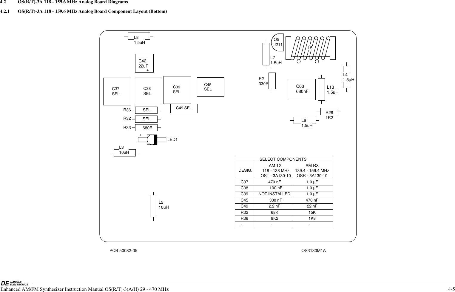
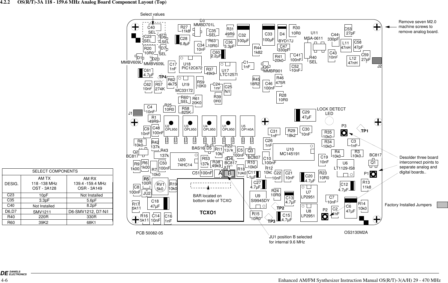
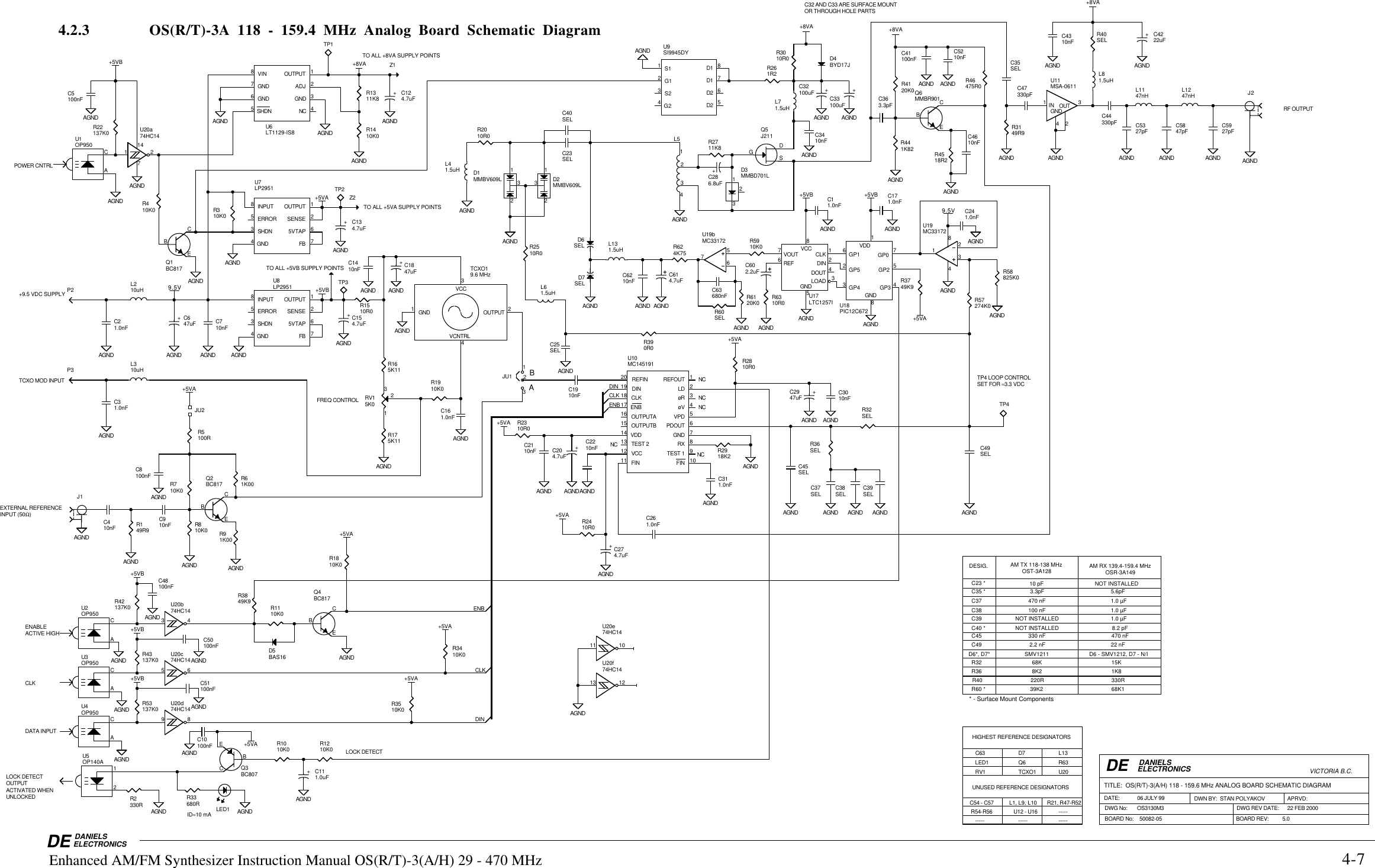
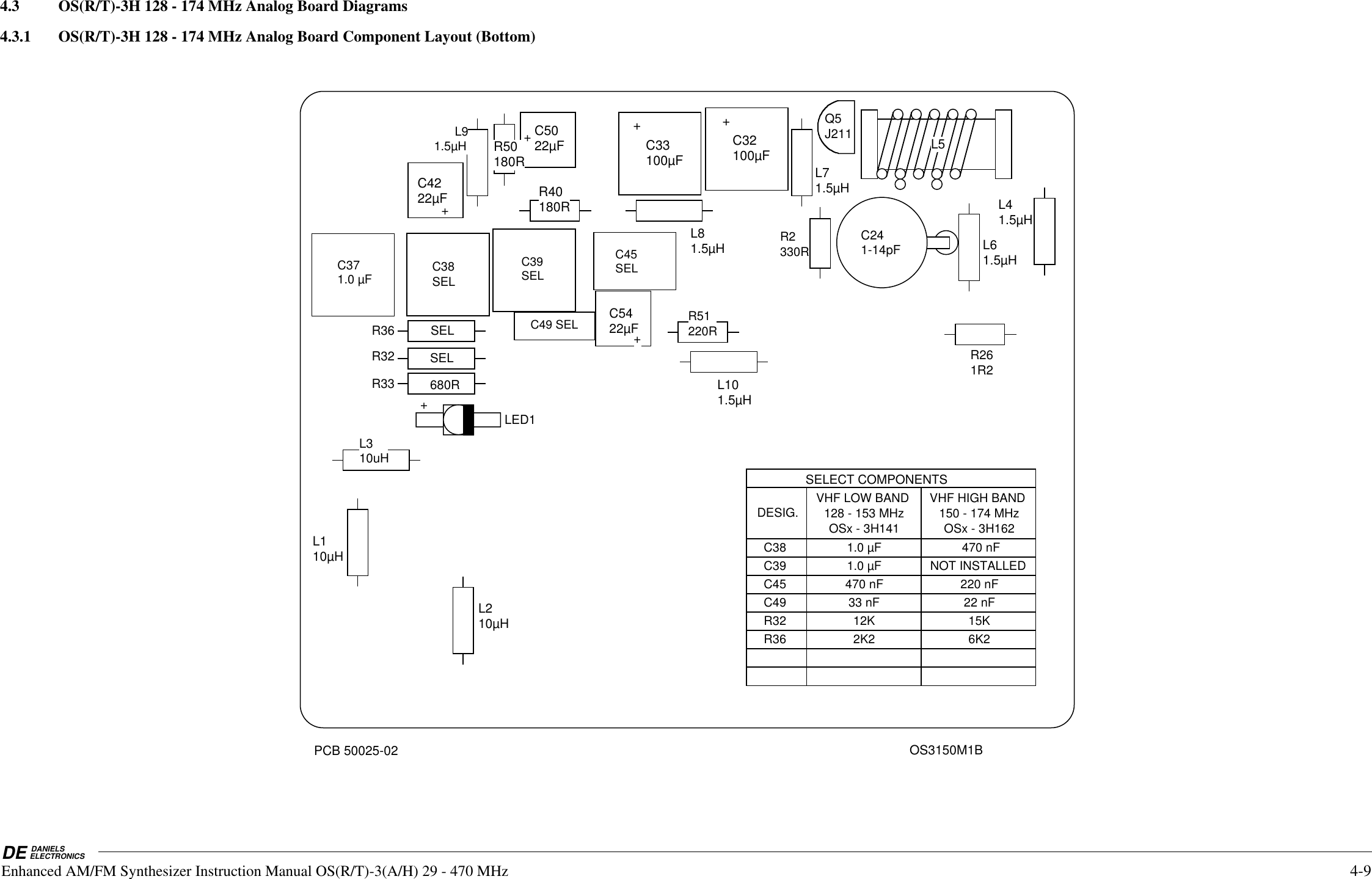
Codan Radio Communications VT-3A130-S-FSH Transmitter User Manual Enhanced AM FM Synthesizer Instruction Manual
Codan Radio Communications Transmitter Enhanced AM FM Synthesizer Instruction Manual
Contents
Enhanced AM FM Synthesizer Instruction Manual
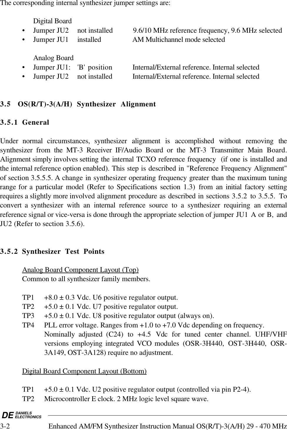
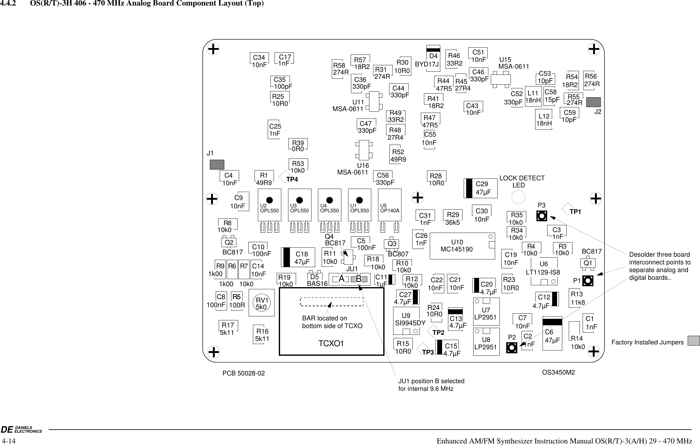
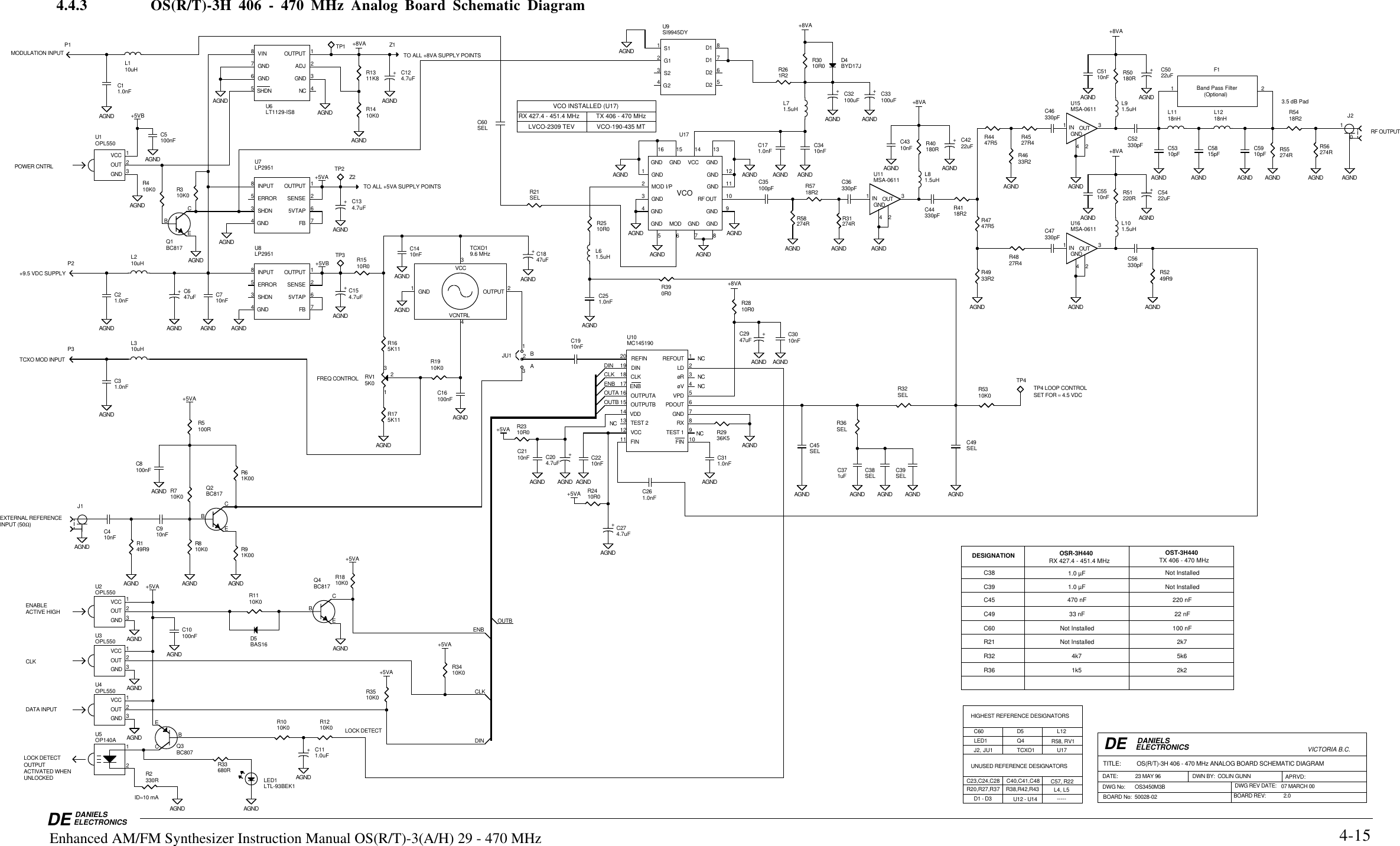
![DEDANIELSELECTRONICSEnhanced AM/FM Synthesizer Instruction Manual OS(R/T)-3(A/H) 29 - 470 MHz 1-31.3 Performance SpecificationsType: NBFM Single loop synthesizer module. Utilizing low noiseVCO and PLL technology. Compatible with Daniels MT-3series transmitter and receiver modules.Frequency Range: 29 MHz - 38 MHz [± 0.5 MHz] (OST-3H035)Tuning range with no adjustment 38 MHz - 50 MHz [± 1.0 MHz] (OST-3H045)shown in [ ] brackets. 50.4 MHz - 71.4 MHz [± 1.0 MHz] (OSR-3H061)118 MHz -138 MHz [Full band] (OST-3A128)128 MHz – 152.6 MHz [± 2.0 MHz] (OST-3H141, OSR-3H141)139.4 MHz - 159.4 MHz [Full band] (OSR-3A149)150 MHz - 174 MHz [± 2.0 MHz] (OST-3H162, OSR-3H162)406 MHz - 470 MHz [Full band] (OST-3H440)427.4 MHz - 451.4 MHz [Full band] (OSR-3H440)Output Power: +5 dBm ±2 dBm into 50ΩHarmonics: <-30 dBcSpurious: <-90 dBc<-70 dBc above 400 MHzAttack Time: <50 ms (Power down mode)Hum and Noise: -55 dBModulation Sensitivity: 3.0 kHz peak deviation / 400 mVrms inputExternal Reference Input: External reference input signal via SMB connector J1Input level 0 dBm ± 3 dB.Input impedance 50ΩInput frequency 10.0 MHz or 9.6 MHz selected throughdigital board jumper JU1.Power Requirements: +9.5 Vdc @ 160 mA for FM and 65 mA for AMStandby mode, TCXO enabled:+9.5 Vdc @ 14 mA for FM and 4 mA for AM](https://usermanual.wiki/Codan-Radio-Communications/VT-3A130-S-FSH.Enhanced-AM-FM-Synthesizer-Instruction-Manual/User-Guide-95210-Page-7.png)
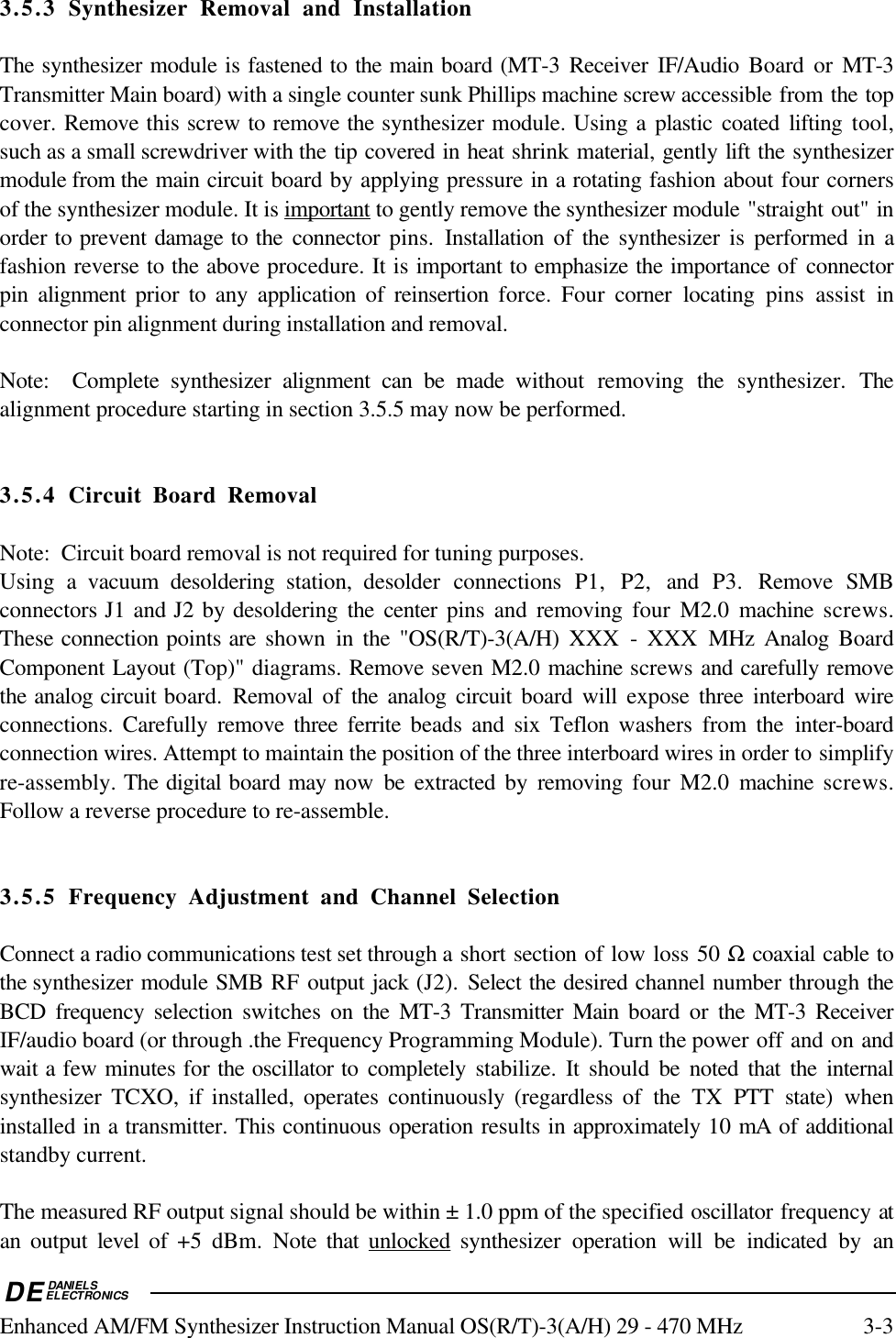
![DE DANIELSELECTRONICS2-8 Enhanced AM/FM Synthesizer Instruction Manual OS(R/T)-3(A/H) 29 - 470 MHz2.6 5.0/6.25 kHz Channelization.The operating frequency is determined as follows for Synthesizers having 5.0/6.25 kHz channelincrement capability;• for BCD switch settings (in the range of 0000 to 4999 , multiply the switchsetting by 5.0 kHz and add it to the synthesizer base frequency.Example: An OST-3H141 synthesizer has a base frequency of 128 MHz. Theselected channel number is 0988. The synthesizer output frequency is:((988 x 5 kHz) + 128 MHz) = 132.940 MHz• for BCD switch settings in the range of 5000 to 9999 , subtract 5000 from theswitch setting, multiplying the result by 6.25 kHz and add it to the synthesizerbase frequency.Example: An OSR-3H162 synthesizer has a base frequency of 150 MHz. Theselected channel number is 7205. The synthesizer output frequency is:((7205-5000) x 6.25 kHz) + 150 MHz) = 163.78125 MHzThe key point to remember is that 5.0 kHz channel increments are selected with BCDchannel switch settings in the range of #0000 through #4999 and 6.25 kHz channelincrements are selected with BCD switch settings in the range of #5000 through #9999.2.7 8.333 kHz Channelization.The operating frequency is determined as follows for Synthesizers having 8.333 kHz channelincrement capability;• Multiply the BCD switch setting by 8.333 kHz and add it to the synthesizerbase frequency.Example: An OST-3A128 synthesizer has a base frequency of 118 MHz. Theselected channel number is 0231. The synthesizer output frequency is:[(1200 x 8.333 kHz) + 118 MHz] = 128.000 MHz](https://usermanual.wiki/Codan-Radio-Communications/VT-3A130-S-FSH.Enhanced-AM-FM-Synthesizer-Instruction-Manual/User-Guide-95210-Page-16.png)