Codan Radio Communications VT-3A130-S-FSH Transmitter User Manual VT3A130 Amplifier Instruction Manual
Codan Radio Communications Transmitter VT3A130 Amplifier Instruction Manual
UserManual.wiki
>
Codan Radio Communications
>
VT-3A130-S-FSH User Manual
>
VT3A130 Amplifier Instruction Manual
Contents
1.
Enhanced AM FM Synthesizer Instruction Manual
2.
Frequency Select Handle Instruction Manual
3.
VHF AM Receiver and Transmitter Channel Designation Tables
4.
MT 3 AM Transmitter Main Board Instruction Manual
5.
VHF AM Transmitter Instruction Manual
6.
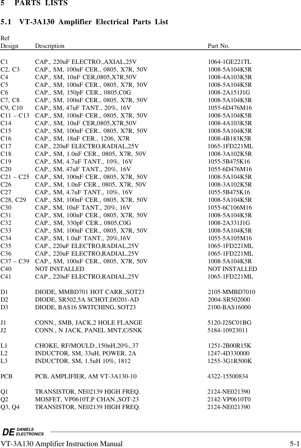
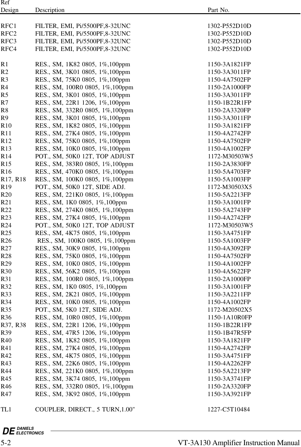
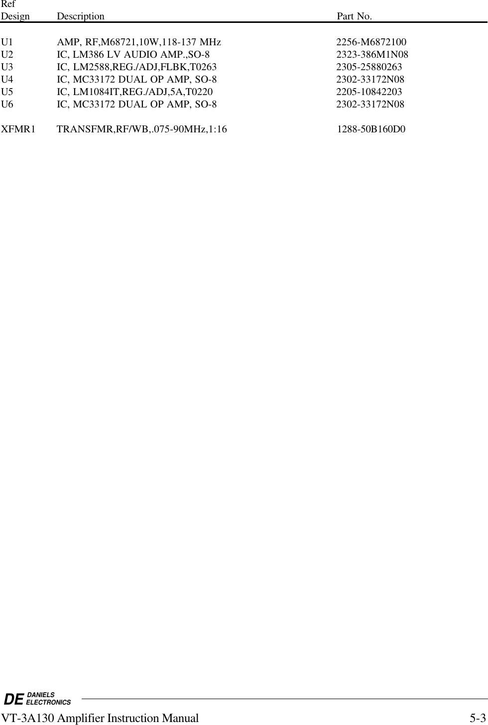
VT3A130 Amplifier Instruction Manual
VT3A130 Amplifier Instruction Manual
Navigation menu
Upload a User Manual
Namespaces
Wiki Guide
HTML
PDF
Info
Views
User Manual
Discussion / Help
Navigation