Codan Radio Communications VT-3A130-S-FSH Transmitter User Manual VT3A130 Amplifier Instruction Manual
Codan Radio Communications Transmitter VT3A130 Amplifier Instruction Manual
Contents
VT3A130 Amplifier Instruction Manual

DANIELS
ELECTRONICS LTD.
TM
MT-3 RADIO SYSTEMS
VT-3A130 AMPLIFIER
INSTRUCTION MANUAL
118 - 138 MHz
Covers the following:
Amplifier portion of VT-3A130-SYD410
Copyright © 2000 Daniels Electronics Ltd. All rights reserved. No part of this publication may be
reproduced, stored in a retrieval system or transmitted in any form or by any means, electronic,
mechanical, photocopying, recording or otherwise, without the prior written consent of Daniels
Electronics Ltd.
DE™ is a registered trademark of Daniels Electronics Ltd. registered in the United States Patent and
Trademark Office.
Issue: 4 Previous Issue: 3
Issue Date: March 2000 Previous Issue Date: March 98 Daniels Electronics Ltd.
Printing Date: March 2000 Victoria, BC.
Part No.: IM22-VT3A130AMP PRINTED IN CANADA

DE DANIELS
ELECTRONICS
ii VT-3A130 Amplifier Instruction Manual
Reviewed By:
Quality Assurance:
Claudia
Boorman
_________________
Name Signature Date
NOTE:
The user's authority to operate this equipment could be revoked through any
changes or modifications not expressly approved by Daniels Electronics Ltd.
The design of this equipment is subject to change due to continuous
development. This equipment may incorporate minor changes in detail from the
information contained in this manual.

DE DANIELS
ELECTRONICS
VT-3A130 Amplifier Instruction Manual iii
TABLE OF CONTENTS Page
1 GENERAL.................................................................................1-1
1.1 Introduction ..........................................................................1-1
1.2 Performance Specification..........................................................1-1
2 THEORY OF OPERATION.............................................................2-1
2.1 General ...............................................................................2-1
2.2 Power Requirements................................................................2-1
2.3 RF Circuitry..........................................................................2-1
2.3.1 VT-3/150 Lowpass Filter .......................................................2-2
2.4 Power Supply Circuitry. ...........................................................2-2
3 VT-3A130 AMPLIFIER ALIGNMENT ...............................................3-1
3.1 General ...............................................................................3-1
3.2 Repair Note ..........................................................................3-1
3.3 Printed Circuitboard Numbering Convention....................................3-1
3.4 Recommended Test Equipment List...............................................3-2
3.5 VT-3A130 Amplifier Alignment...................................................3-2
3.5.1 General ............................................................................3-2
3.5.2 VT-3A130 Amplifier Adjustment ..............................................3-2
3.5.3 Changing Power Output.........................................................3-3
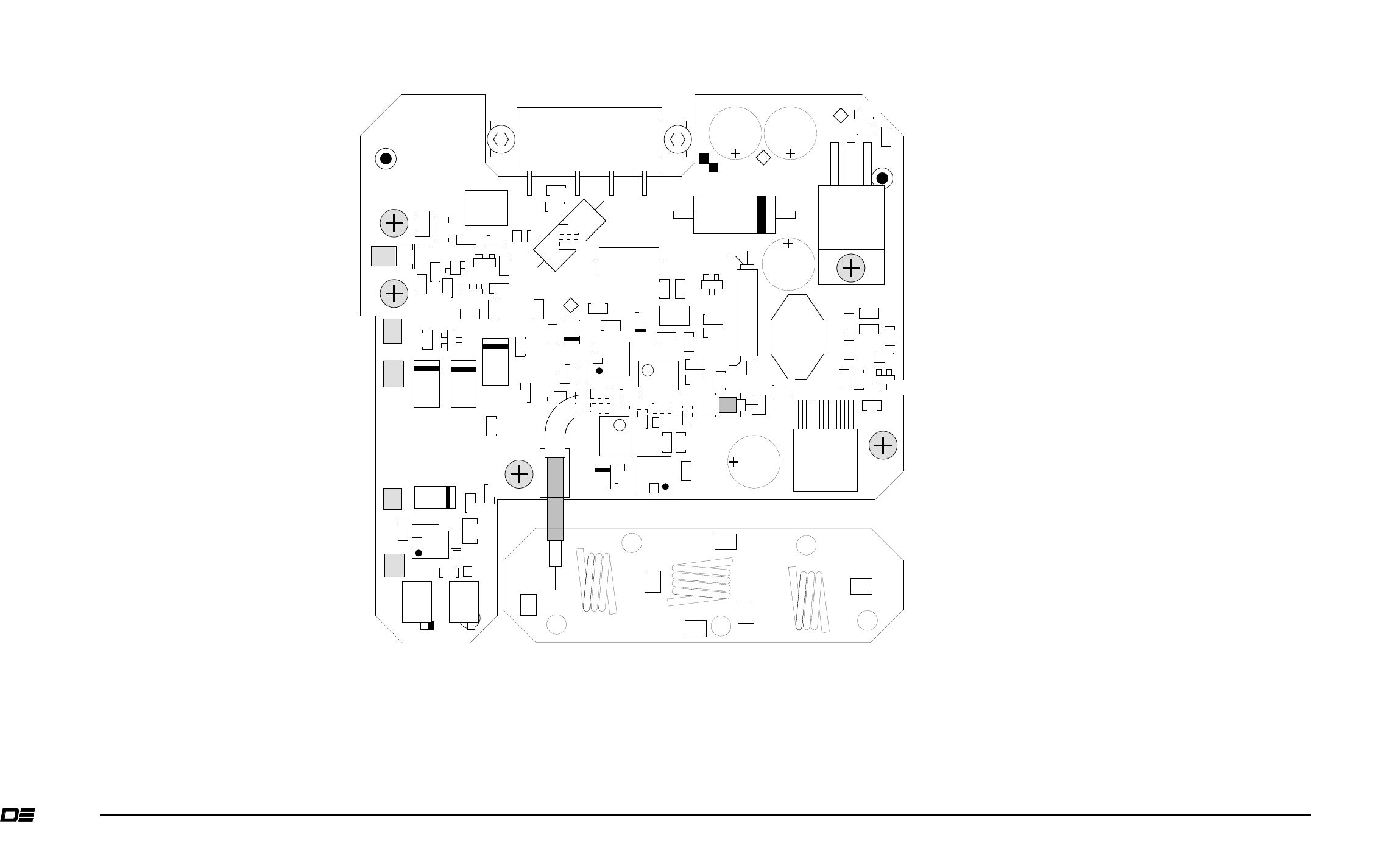
4 ILLUSTRATIONS AND SCHEMATIC DIAGRAMS ..............................4-1
4.1 VT-3A130 Amplifier................................................................4-1
4.1.1 VT-3A130 Amplifier Component Layout .....................................4-2
4.1.2 VT-3A130 Amplifier Schematic Diagram .....................................4-3
4.2 VT-3A130 Lowpass Filter .........................................................4-5
4.2.1 VT-3A130 Lowpass Filter Component Layout...............................4-5
4.2.2 VT-3A130 Lowpass Filter Schematic Diagram...............................4-5
5 PARTS LISTS ............................................................................5-1
5.1 VT-3A130 Amplifier Electrical Parts List ........................................5-1
5.2 VT-3A130 Lowpass Filter Electrical Parts List..................................5-4
5.3 VT-3A130 Amplifier Mechanical Parts List......................................5-4
6 REVISION HISTORY ...................................................................6-1

DE DANIELS
ELECTRONICS
iv VT-3A130 Amplifier Instruction Manual
This Page Intentionally Left Blank

DE DANIELS
ELECTRONICS
VT-3A130 Amplifier Instruction Manual 1-1
1 GENERAL
1.1 Introduction
The VT-3A130 Amplifier provides the final stage of RF amplification and filtering for the VT-3A
Transmitters. The output power is 1.0 - 4.0 Watt adjustable (carrier only). The amplifier operates
over 118MHz - 138 MHz frequency range without tuning.
Output filtering for the VT-3A130 Amplifier is provided by an Output Lowpass Filter Board. The
Output Lowpass Filter Board is mounted in a separate compartment of the amplifier case in order to
provided maximum attenuation of harmonic and other spurious signals.
Refer to section 4.1.2 "VT-3A130 Amplifier Schematic Diagram" for the Amplifier schematic
diagram and section 4.1.3 for the Output Lowpass Filter component layout and schematic diagram.
1.2 Performance Specification
Type: VT-3 series VHF Amplifier module
Family: VT-3A130
Frequency Range: 118.0 MHz to 138.0 MHz
RF Power Output: 1.0 - 4.0 Watts adjustable (carrier only)
RF Power Input Nominal level from -5 dBm to +5 dBm
System Impedance: 50 Ω
Spurious and Harmonics Emissions: More than 90 dB below carrier
Modulation: 6K00A3 (Amplitude Modulation)
Transmitted Noise More than 45 dBc below carrier
Audio Response: Flat audio; +1/-3 dB: 300 Hz - 3 kHz
Audio Distortion: Less than 3% -40˚C to +60˚C at 30% modulation
Less than 5% -40˚C to +60˚C at 90% modulation
Load VSWR tolerance: Z load = 20:1:
Operating Voltage: +13.8 Vdc Nominal (range +10 to +17 Vdc),
+9.5 Vdc Regulated.
Active Current: +13.8 Vdc supply less than 1.5 A at Pout=4
Standby Current: Typically less than 4 mA

DE DANIELS
ELECTRONICS
1-2 VT-3A130 Amplifier Instruction Manual
Amplifier Enable: Active to ground.
Output Power Rise Time (10-90% of Less than 20 ms
steady state value)
Output Power Fall Time (90-10% of Less than 10ms
Steady state value)
Key-On/Key-off Spectral Mask Transients are at least 80 dBc for frequencies
± 400 kHz from carrier.
Operating Temperature Range: -30˚C to +60˚C, optional - 40˚C temperature test.
Operating Humidity: 95% Relative Humidity (Non-condensing) at
+25°C

DE DANIELS
ELECTRONICS
VT-3A130 Amplifier Instruction Manual 2-1
2 THEORY OF OPERATION
2.1 General
VT-3A130 Amplifier is a Class A linear amplifier with a low level AM modulator. A built in
regulated power supply provides approximately 15.0Vdc output voltage with the input voltage
range of 10.0 Vdc to 17 Vdc. This amplifier utilizes a 10 Watt hybrid power amplifier module
manufactured by Mitsubishi. The module is mounted directly to the heatsink with its leads soldered
to a circuit board where DC supply voltage and RF input and output connections are made.
Power for the VT-3A130 Amplifier is provided from +13.8 Vdc and 9.5Vdc supplies. The
supplies can be continuously connected to the amplifier. The VT-3A130 Amplifier will draw only
about 4 mA of current from +13.8 Vdc and about 0.1 mA from 9.5Vdc until the AMPLIFIER
ENABLE pin is grounded.
The VT-3A130 Amplifier is housed in a machined aluminum case that ensures optimum RF
shielding, provides a good ground, and also acts as a heatsink.
2.2 Power Requirements
The current drawn from the +9.5 Vdc supply should not exceed 10 mA. Current consumption of
the +13.8 Vdc line is dependent on transmitter frequency, output power, temperature, and supply
voltage and can range from 800 mA to 1500 mA. The current drawn from the +13.8 Vdc supply
should not exceed 1500 mA under normal circumstances and should never be allowed to exceed
1700 mA.
2.3 RF Circuitry
Refer to Section 4.1.2 "VT-3A130 Amplifier Schematic Diagram". The RF input signal with a
level of -5 dBm to +5 dBm is fed to the VT-3A130 Amplifier Board and then is modulated by a
balanced AM Modulator which consists of Q1, Q3, Q4, and a wide band RF transformer XFMR1.
Q1, Q3 collectors are supplied by 15.0 Vdc in order to increase the modulation linearity. On the
contrary, the base circuitry of Q1, Q3 and Q4 are biased by 9.5 Vdc. The typical output power
from the Modulator is about 3dBm to 5 dBm. The signal is then amplified further by a Hybrid
Power Amplifier Module U1, which is the class A, 10 watt linear amplifier. The U1 is supplied
from a 15.0Vdc internal regulated power supply. Maximum carrier power output is 4 - 5 watt for
the input voltage range from 10 Vdc to 17 Vdc. Output filtering for the VT-3A130 Amplifier is
provided by a Low Pass Filter Board. The Low Pass filter assembly is mounted in a separate
compartment of the amplifier case in order to provided maximum attenuation of harmonic and other
spurious signals. Refer to Section 4.1.1 "VT-3A130 Amplifier Component Layout"

DE DANIELS
ELECTRONICS
2-2 VT-3A130 Amplifier Instruction Manual
The part of the output RF energy is coupled by a directional detector circuit TL1 which provides a
means of linearization of the audio and leveling of the output power over the frequency range 118
MHz to 138 MHz.
The AC coupled audio signal is applied to the inverting input of U4a in order to provide
predistortions to the input modulation audio signal, which is supplied from the audio amplifier U2
to the non-inverting input of U4a.
On the contrary the DC coupled part of the detected audio is passed through the 50Hz low pass
filter U6a, U6b, and than compared with a certain DC level which is set by R19. The difference of
the signals is amplified by U4b and applied to pin 2 of the Power Amplifier Module in order to
keep the output power relatively constant over the frequency range of 118MHz to 138MHz.
2.3.1 VT-3/150 Lowpass Filter
The VT-3/150 Output Lowpass Filter is a 50 ohm, 6 pole, reciprocal filter with a 3 dB cutoff
frequency of approximately 150 MHz. The low pass filter assembly attenuates the desired signal's
harmonics as well as any other out-of-band emissions so that a 'clean' RF signal is output to the
antenna connector.
2.4 Power Supply Circuitry.
The VT-3A130 Amplifier has shutdown circuitry based on Q2 that allows decrease power
consumption, less than 0.1 mA from 9.5Vdc, in standby mode. The voltage level on the amplifier
enable line of less than +2.0 Vdc turns on the transistor Q2. Q2 supplies the base circuitry of Q1,
Q3, Q4, and operational amplifiers U2, U4, and U6.
The U3 LM2588 used as a step-up (boost) regulator. This is a switching regulator that produces an
output voltage greater than the input supply voltage. The following is the LM1084ADJ, a low
dropout voltage (LDO) positive adjustable regulators with a maximum dropout of 1.5V at 5A of
load current. The LM1084 used as a postregulator that reduces the ripple current and also prevents
the output voltage level from overshooting the maximum of 16Vdc.

DE DANIELS
ELECTRONICS
VT-3A130 Amplifier Instruction Manual 3-1
3 VT-3A130 AMPLIFIER ALIGNMENT
3.1 General
Connections to the power supply, audio input and transmit enable line are clearly marked on the
amplifier case. The amplifier is enabled when the enable line (AMPLIFIER ENABLE pin) is
grounded.
If the amplifier is installed in the transmitter, alignment is simplified by using the SR-3 Subrack,
SM-3 System Monitor, and RF extender cable to provide transmitter power and signal
interconnection (see the Transmitter Main Board Manual for details). For complete transmitter
alignment, the Transmitter Main Board, Synthesizer, Amplifier, and Audio Processor should be
tuned in the aforementioned order. Please refer the corresponding manuals for each module.
3.2 Repair Note
The VT-3A130 Amplifier is mainly made up of surface mount devices which should not be
removed or replaced using an ordinary soldering iron. Removal and replacement of surface mount
components should be performed only with specifically designed surface mount rework and repair
stations complete with ElectroStatic Dissipative (ESD) protection.
When removing Surface Mount Solder Jumpers, it is recommended to use solder braid in place of
manual vacuum type desoldering tools when removing jumpers. This will help prevent damage to
the circuit boards.
3.3 Printed Circuitboard Numbering Convention
To ease troubleshooting and maintenance procedures, Daniels Electronics Limited has adopted a
printed circuitboard (PCB) numbering convention in which the last two digits of the circuitboard
number represent the circuitboard version. For example:
• PCB number 43-9120
10
indicates circuitboard version 1.0;
• PCB number 50002-
02
indicates circuitboard version 2.0.
All PCB's manufactured by Daniels Electronics are identified by one of the above conventions.

DE DANIELS
ELECTRONICS
3-2 VT-3A130 Amplifier Instruction Manual
3.4 Recommended Test Equipment List
Alignment of the transmitter requires the following test equipment or its equivalent.
Dual Power Supply: Regulated +9.5 Vdc at 0.1 A.
Regulated +13.8 Vdc at 2 A - Topward TPS-4000
Oscilloscope / Multimeter: Fluke 97 Scopemeter
Current Meter: Fluke 75 multimeter
Radio communications test set: Marconi Instruments 2955R
VSWR 3:1 mismatch load: JFW 50T-035-3.0:1
Alignment Tool: Johanson 8766
3.5 VT-3A130 Amplifier Alignment
3.5.1 General
The VT-3A130 Amplifier is a module that is factory assembled to operate in the frequency band:
118MHz to 138MHz. The amplifier requires -5 dBm to 5 dBm of input power and is continuously
adjustable over its power range of 1.0 to 4.0 Watts.
3.5.2 VT-3A130 Amplifier Adjustment
1. Apply power to the amplifier's +13.8 Vdc and +9.5Vdc pins. The +9.5 Vdc power
supply must be well regulated.
2. Connect the amplifier's antenna output connector to the type N input of the radio
communications test set through a short section of low loss 50 Ω coaxial cable.
3. Turn the two of the adjustment potentiometers POWER ADJUST pot R19 and
AUDIO ADJUST pot R35 fully counterclockwise.
4. Turn DISTORTION ADJUST pot R14 and POWER CONTROL ADJUST pot R24
to its center position
6. Apply a non-modulated 118 MHz RF signal of - 5 dBm / +5 dBm to the RF INPUT
connector.
7. Turn on the amplifier by applying a ground to the amplifier ENABLE INPUT pin.
8. Adjust POWER ADJUST pot R19 so that the output power is about 4Watt by turning
it clockwise. Do not let the current through the transistor U1 exceed 1.5 A on the
+13.8 Vdc line.

DE DANIELS
ELECTRONICS
VT-3A130 Amplifier Instruction Manual 3-3
9. Apply a 1000 Hz signal with 0.200 Vrms level to the amplifier's
MODULATION INPUT and adjust AUDIO ADJUST pot R35 to obtain 90% of AM
modulation.
10. Adjust the DISTORTION ADJUST pot R14 to the lowest distortion (less than 5%)
11. Change the RF signal frequency to 128 MHz, 138 MHz and control the Modulation
Level and Output Power (with no modulation).
12. Re-adjust the AUDIO ADJUST pot R35 (if it necessarily) so that the modulation level
do not exceed 90% at 128 MHz and 138 MHz frequencies.
13. Re-adjust the POWER ADJUST pot R19 (if it necessarily) to achieve a minimum
tolerance of the output power (4 Watt +/- 1dB).
3.5.3 Changing Power Output
The power amplifier's carrier output level can be adjusted from 1.0 to 4.0 watts. To
change the RF output level, follow the procedures described below.
1. Apply power to the amplifier's +13.8 Vdc and +9.5Vdc pins. The +9.5 Vdc power
supply must be well regulated.
2. Connect the amplifier's antenna output connector to the type N input of the radio
communications test set through a short section of low loss 50 Ω coaxial cable.
3. The amplifier requires -5 dBm to 5 dBm of RF power
4. Turn on the amplifier by applying a ground to the AMPLIFIER ENABLE pin.
5. Adjust the POWER ADJUST pot R19 to achieve the desired RF carrier power output
between 1.0 Watt and 4.0 Watt.
6. Apply a 1000 Hz signal with 0.200Vrms level to the power amplifier's
MODULATION INPUT and adjust AUDIO ADJUST pot R35 to obtain 90% of modulation.

DE DANIELS
ELECTRONICS
3-4 VT-3A130 Amplifier Instruction Manual
This Page Intentionally Left Blank

DE DANIELS
ELECTRONICS
VT-3A130 Amplifier Instruction Manual 4-1
4 ILLUSTRATIONS AND SCHEMATIC DIAGRAMS
4.1 VT-3A130 Amplifier
This Page Intentionally Left Blank
VICTORIA B.C .
DANIELS
ELECTRONICS
D
DATE: 04 MAY 99 DRAWN BY: SHANE A
DWG No: 50083AS1 DWG REV DATE: 22 FEB 2000
TITLE: AM WIDEBAND TX AMP
PCB 50083-04
TITLE: AM WIDEBAND TX AMP SURFACE MOUNT LAYOUT
R35
5k0 R19
50k0
R22
274k
R21
1k0
U2
LM386 R36
10R0
C15
100nF
C30
10µF C21
100nF
R20
221k
C9
47µF
C20
47µF
C10
47µF
Q2
VP0610T
C39
100nF
R46
332R R45
3k74
U3
LM2588
R6
N\I
R40
1k82
C40
N\I
D3
BAS16
R44
221k
R43
22k6
R42
4k75
R41
27k4
C7
100nF
C8
100nF
D1
MMBD701
L3
1.5µH
C38
100nF
C25
100nF
R16
470k
C22
100nF
R4
100R
R17
100k
C24
100nF
C16
18nF
C28
100nF
R15
383R
C37
100nF
C14
10nF
C18
1nF
C19
4.7µF
R12
75k R28
75k
U4
MC33172
U6
MC33172
R24
50k0
R14
50k0
C27
4.7µF
C26
1nF
R18
100k
C23
100nF
C29
100nF
C34
1µF
R5
3k01 C6
150pF
R29
10k
R26
100k
R13
10k R3
75k R11
27k4 R25
4k75
C31
100nF
R27
30k9
R23
27k4
R32
1k0
R33
2k21
R34
10k0
R31
100R
R10
1k82
C13
100nF
R7
22R1
C4 10nF
R1
1k82
R2
3k01
C11
100nF R8
332R
R9
3k01
Q4
NE02139
Q1
NE02139
Q3
NE02139
XFMR1
TTWB
R37
22R1
R38
22R1
R39
47R5
R30
56k2
C12
100nF
C2
100nF
C3
100nF
C33
100nF
L2
33µH
C5
100nF C32
330pF
R47
3k92
DWG No: 50083AS2
TITLE: AM WIDEBAND TX AMP THROUGH HOLE LAYOUT & DESIG
U1
M68721
TL1
C17
220µH
C36
220µH
C41
220µH
C35
220µH
D2
SR502 U5
LM1084
L1
1.5µH
C1
220µH
DWG No: 50083AT1
TP1
TP3
TP2
R3
75k R11
27k4 R25
4k75
R27
30k9
C5
100nF C32
330pF
ELECTRONICS LTD.
DANIELS TM
4-2
4.1.1 VT-3A130 Amplifier Component Layout
VT-3A130 Amplifier Instruction Manual
PCB 50086-01 VT3A130AMPM1B
C33
100nF
C3
100nF
C1
C2
C5
VT-3A130 Lowpass Filter Assembly
VICTORIA B.C.
ELECTRONICS LTD.
DANIELS
ELECTRONICS LTD.
DANIELS
Appr. 15.5 Vdc
Appr. 16.5 Vdc
TITLE: VT-3A-130 AMPLIFIER SCHEMATIC DIAGRAM
DWG No: VT3A130AMPM2B
4-3
VT-3A130 Amplifier Instruction Manual
4.1.2 VT-3A130 Amplifier Schematic Diagram
DWG REV DATE: 9 MARCH 2000
C42
R47
-----
----- ----- -----
TL1, TP3
D3
BOARD No: 50083-04 BOARD REV: 04
L3
8dB Att.
DATE: 23 JUNE 1999
U6, XFMR1
RFC4
Q4
J2
DWN BY: STAN POLYAKOV
Power control adjust
2.5Vdc - 3.5Vdc
Power adjust
Distortion adjust
50Hz Low Pass Filter
APRVD:
HIGHEST REFERENCE DESIGNATORS
UNUSED REFERENCE DESIGNATORS
-----
-----
-----
-----
-----
D1
MMBD701
C6
150pF
1
9.5Vdc
RFC1
5500PF
RFC2
5500PF
1
AMPLIFIER ENABLE
C13
100nF
RFC3
5500PF
1
10 - 17 Vdc
4
3
2
1
8
U4
MC33172
a
9.5V
C18
1.0nF C19
4.7uF
75K0
R12
123
50K0
R14
75K0
R3
8
3
21
4
U6
MC33172
a
R17
100K0
6
5
7
U6
MC33172
b
6
5
7
U4
MC33172
b
R16
470K0
9.5V
C26
1.0nF C27
4.7uF
123
50K0
R24
R26
100K0
RFC4
5500PF
1
AUDIO IN
C25
100nF
1
2
SMA
J2
L3
1.5uH
9.5V
75K0
R28
TP2
R25
4K75
R21
1K0
R22
274K0
R23
27K4
R29
10K0
R30
56K2
C4
10nF
G
DS
Q2
VP0610T
12
FIL1
LOW PASS FILTER
E
B
C
Q1
NE02139
E
B
C
Q3
NE02139
R1
1K82
R2
3K01 R7
22R1
R9
3K01
R10
1K82
R31
100R0
R33
2K21
R34
10K0
E
B
C
Q4
NE02139
9.5V
47uF
C10 47uF
C20
C11
100nF
1
2
SMB
J1
TO ALL 9.5V SUPPLY POINTS
47uF
C9
100nF
C3
L1
150nH
10nF
C14
R11
27K4
1
2
3
4
5
6
7
8LM386
U2
1
2
35K0
R35
100nF
C15
9.5V
18nF
C16
10R0
R36
100nF
C28
10uF
C30
C21
100nF
118-138 MHz
RF RF
OUTIN
23
14
M68721
U1
13
645
XFMR1
TTWB-4-B
12
34
TL1
0.5" COAX
1
2
350K0
R19
332R0
R8
330pF
C32
10K0
R13
30K9
R27
100nF
C12
100nF
C2
100nF
C5
R18
100K0
C31
100nF
C23
100nF
C29
100nF
C22
100nF
22R1
R37 22R1
R38
R39
47R5
15V
SR502
D2
383R0
R15
C37
100nF
C38
100nF
100R0
R4
3K01
R5
GND
FEED
BACK
COMP
IN SWITCH
ON/OFF
2
4
3
75
1
LM2588
U3
100nF
C8
D3
BAS16
15V
N/I
R6
33uH
L2
ADJ
OUT
IN
3
21
LM1084
U5 TO ALL 15V
220uF
C35
220uF
C36
27K4
R41
TP1 TP3
220uF
C17
C39
100nF
100nF
C7
1K82
R40
N/I
C40
220uF
C41
R46
332R0
100nF
C33
C24
100nF
3K74
R45
R20
221K0
1.0uF
C34
R44
221K0
R43
22K6
4K75
R42 3K92
R47
220uF
C1
R32
1K00

DE DANIELS
ELECTRONICS
4-4 VT-3A130 Amplifier Instruction Manual
This Page Intentionally Left Blank
DE DANIELS
ELECTRONICS
VT-3A130 Amplifier Instruction Manual 4-5
4.2 VT-3A130 Lowpass Filter
4.2.1 VT-3A130 Lowpass Filter Component Layout
PCB 50086-01
C1
15pF
C2
7.5pF
C5
4.7pF
24pF
C6
30pF
C4
30pF
C3
L1
L2
L3
VT3A130AMPM3A
4.2.2 VT-3A130 Lowpass Filter Schematic Diagram
VICTORIA B.C.
ELECTRONICS LTD.
DANIELS
DWG No: VT3A130AMPM4A
DATE: 02 JUNE 1999
TITLE: VT-3A130 LOW PASS FILTER
DWN BY: STAN POLYAKOV
L3C6
BOARD No: 50086-01 BOARD REV: 01
DWG REV DATE:
RF INPUT RF OUTPUT
HIGHEST REFERENCE DESIGNATORS
UNUSED REFERENCE DESIGNATORS
-----
-----
-----
-----
-----
-----
-----
-----
-----
-----
-----
-----
-----
-----
-----
-----
APRVD:
C1
15pF
L1
3.0 TURNS
C3
30pF C4
30pF
L2
4.0 TURNS
C5
4.7pF
L3
3.0 TURNS
C2
7.5pF C6
24pF

DE DANIELS
ELECTRONICS
4-6 VT-3A130 Amplifier Instruction Manual
This Page Intentionally Left Blank

DE DANIELS
ELECTRONICS
VT-3A130 Amplifier Instruction Manual 5-1
5 PARTS LISTS
5.1 VT-3A130 Amplifier Electrical Parts List
Ref
Design Description Part No.
C1 CAP., 220uF ELECTRO.,AXIAL,25V 1064-1GE221TL
C2, C3 CAP., SM, 100nF CER., 0805, X7R, 50V 1008-5A104K5R
C4 CAP., SM, 10nF CER,0805,X7R,50V 1008-4A103K5R
C5 CAP., SM, 100nF CER., 0805, X7R, 50V 1008-5A104K5R
C6 CAP., SM, 150pF CER., 0805,C0G 1008-2A151J1G
C7, C8 CAP., SM, 100nF CER., 0805, X7R, 50V 1008-5A104K5R
C9, C10 CAP., SM, 47uF TANT., 20%, 16V 1055-6D476M16
C11 – C13 CAP., SM, 100nF CER., 0805, X7R, 50V 1008-5A104K5R
C14 CAP., SM, 10nF CER,0805,X7R,50V 1008-4A103K5R
C15 CAP., SM, 100nF CER., 0805, X7R, 50V 1008-5A104K5R
C16 CAP., SM, 18nF CER., 1206, X7R 1008-4B183K5R
C17 CAP., 220uF ELECTRO,RADIAL,25V 1065-1FD221ML
C18 CAP., SM, 1.0nF CER., 0805, X7R, 50V 1008-3A102K5R
C19 CAP., SM, 4.7uF TANT., 10%, 16V 1055-5B475K16
C20 CAP., SM, 47uF TANT., 20%, 16V 1055-6D476M16
C21 – C25 CAP., SM, 100nF CER., 0805, X7R, 50V 1008-5A104K5R
C26 CAP., SM, 1.0nF CER., 0805, X7R, 50V 1008-3A102K5R
C27 CAP., SM, 4.7uF TANT., 10%, 16V 1055-5B475K16
C28, C29 CAP., SM, 100nF CER., 0805, X7R, 50V 1008-5A104K5R
C30 CAP., SM, 10uF TANT., 20%, 16V 1055-6C106M16
C31 CAP., SM, 100nF CER., 0805, X7R, 50V 1008-5A104K5R
C32 CAP., SM, 330pF CER., 0805,C0G 1008-2A331J1G
C33 CAP., SM, 100nF CER., 0805, X7R, 50V 1008-5A104K5R
C34 CAP., SM, 1.0uF TANT., 20%,16V 1055-5A105M16
C35 CAP., 220uF ELECTRO,RADIAL,25V 1065-1FD221ML
C36 CAP., 220uF ELECTRO,RADIAL,25V 1065-1FD221ML
C37 – C39 CAP., SM, 100nF CER., 0805, X7R, 50V 1008-5A104K5R
C40 NOT INSTALLED NOT INSTALLED
C41 CAP., 220uF ELECTRO,RADIAL,25V 1065-1FD221ML
D1 DIODE, MMBD701 HOT CARR.,SOT23 2105-MMBD7010
D2 DIODE, SR502,5A SCHOT,D0201-AD 2004-SR502000
D3 DIODE, BAS16 SWITCHING, SOT23 2100-BAS16000
J1 CONN., SMB, JACK,2 HOLE FLANGE 5120-J2SC01BG
J2 CONN., N JACK, PANEL MNT,C/SNK 5184-10923011
L1 CHOKE, RF/MOULD.,150nH,20%,.37 1251-2B00R15K
L2 INDUCTOR, SM, 33uH, POWER, 2A 1247-4D330000
L3 INDUCTOR, SM, 1.5uH 10%, 1812 1255-3G1R500K
PCB PCB, AMPLIFIER, AM VT-3A130-10 4322-15500834
Q1 TRANSISTOR, NE02139 HIGH FREQ. 2124-NE021390
Q2 MOSFET, VP0610T,P CHAN.,SOT-23 2142-VP0610T0
Q3, Q4 TRANSISTOR, NE02139 HIGH FREQ. 2124-NE021390

DE DANIELS
ELECTRONICS
5-2 VT-3A130 Amplifier Instruction Manual
Ref
Design Description Part No.
RFC1 FILTER, EMI, Pi/5500PF,8-32UNC 1302-P552D10D
RFC2 FILTER, EMI, Pi/5500PF,8-32UNC 1302-P552D10D
RFC3 FILTER, EMI, Pi/5500PF,8-32UNC 1302-P552D10D
RFC4 FILTER, EMI, Pi/5500PF,8-32UNC 1302-P552D10D
R1 RES., SM, 1K82 0805, 1%,100ppm 1150-3A1821FP
R2 RES., SM, 3K01 0805, 1%,100ppm 1150-3A3011FP
R3 RES., SM, 75K0 0805, 1%,100ppm 1150-4A7502FP
R4 RES., SM, 100R0 0805, 1%,100ppm 1150-2A1000FP
R5 RES., SM, 3K01 0805, 1%,100ppm 1150-3A3011FP
R7 RES., SM, 22R1 1206, 1%,100ppm 1150-1B22R1FP
R8 RES., SM, 332R0 0805, 1%,100ppm 1150-2A3320FP
R9 RES., SM, 3K01 0805, 1%,100ppm 1150-3A3011FP
R10 RES., SM, 1K82 0805, 1%,100ppm 1150-3A1821FP
R11 RES., SM, 27K4 0805, 1%,100ppm 1150-4A2742FP
R12 RES., SM, 75K0 0805, 1%,100ppm 1150-4A7502FP
R13 RES., SM, 10K0 0805, 1%,100ppm 1150-4A1002FP
R14 POT., SM, 50K0 12T, TOP ADJUST 1172-M30503W5
R15 RES., SM, 383R0 0805, 1%,100ppm 1150-2A3830FP
R16 RES., SM, 470K0 0805, 1%,100ppm 1150-5A4703FP
R17, R18 RES., SM, 100K0 0805, 1%,100ppm 1150-5A1003FP
R19 POT., SM, 50K0 12T, SIDE ADJ. 1172-M30503X5
R20 RES., SM, 221K0 0805, 1%,100ppm 1150-5A2213FP
R21 RES., SM, 1K0 0805, 1%,100ppm 1150-3A1001FP
R22 RES., SM, 274K0 0805, 1%,100ppm 1150-5A2743FP
R23 RES., SM, 27K4 0805, 1%,100ppm 1150-4A2742FP
R24 POT., SM, 50K0 12T, TOP ADJUST 1172-M30503W5
R25 RES., SM, 4K75 0805, 1%,100ppm 1150-3A4751FP
R26 RES., SM, 100K0 0805, 1%,100ppm 1150-5A1003FP
R27 RES., SM, 30K9 0805, 1%,100ppm 1150-4A3092FP
R28 RES., SM, 75K0 0805, 1%,100ppm 1150-4A7502FP
R29 RES., SM, 10K0 0805, 1%,100ppm 1150-4A1002FP
R30 RES., SM, 56K2 0805, 1%,100ppm 1150-4A5622FP
R31 RES., SM, 100R0 0805, 1%,100ppm 1150-2A1000FP
R32 RES., SM, 1K0 0805, 1%,100ppm 1150-3A1001FP
R33 RES., SM, 2K21 0805, 1%,100ppm 1150-3A2211FP
R34 RES., SM, 10K0 0805, 1%,100ppm 1150-4A1002FP
R35 POT., SM, 5K0 12T, SIDE ADJ. 1172-M20502X5
R36 RES., SM, 10R0 0805, 1%,100ppm 1150-1A10R0FP
R37, R38 RES., SM, 22R1 1206, 1%,100ppm 1150-1B22R1FP
R39 RES., SM, 47R5 1206, 1%,100ppm 1150-1B47R5FP
R40 RES., SM, 1K82 0805, 1%,100ppm 1150-3A1821FP
R41 RES., SM, 27K4 0805, 1%,100ppm 1150-4A2742FP
R42 RES., SM, 4K75 0805, 1%,100ppm 1150-3A4751FP
R43 RES., SM, 22K6 0805, 1%,100ppm 1150-4A2262FP
R44 RES., SM, 221K0 0805, 1%,100ppm 1150-5A2213FP
R45 RES., SM, 3K74 0805, 1%,100ppm 1150-3A3741FP
R46 RES., SM, 332R0 0805, 1%,100ppm 1150-2A3320FP
R47 RES., SM, 3K92 0805, 1%,100ppm 1150-3A3921FP
TL1 COUPLER, DIRECT., 5 TURN,1.00" 1227-C5T10484

DE DANIELS
ELECTRONICS
VT-3A130 Amplifier Instruction Manual 5-3
Ref
Design Description Part No.
U1 AMP, RF,M68721,10W,118-137 MHz 2256-M6872100
U2 IC, LM386 LV AUDIO AMP.,SO-8 2323-386M1N08
U3 IC, LM2588,REG./ADJ,FLBK,T0263 2305-25880263
U4 IC, MC33172 DUAL OP AMP, SO-8 2302-33172N08
U5 IC, LM1084IT,REG./ADJ,5A,T0220 2205-10842203
U6 IC, MC33172 DUAL OP AMP, SO-8 2302-33172N08
XFMR1 TRANSFMR,RF/WB,.075-90MHz,1:16 1288-50B160D0

DE DANIELS
ELECTRONICS
5-4 VT-3A130 Amplifier Instruction Manual
5.2 VT-3A130 Lowpass Filter Electrical Parts List
Ref
Desig Description Part No.
C1 CAP., SM, 15pF PORCEL.,+-5%500V 1036-1B2150J5
C2 CAP., SM, 7.5pF PORCEL.,+-.25pF 1036-0B2759C5
C3, C4 CAP., SM, 30pF PORCEL., 5%,500V 1036-1B2300J5
C5 CAP., SM, 4.7pF PORCEL.,+-.25pF 1036-0B2479C5
C6 CAP., SM, 24pF PORCEL., 5%,500V 1036-1B2240J5
PCB PCB, LPF,TX AMP,AM VT-3A130-10 4322-16500861
L1 COIL, 3 TURNS,18AWG,6.35 mm ID 1220-3T001622
L2 COIL, 4 TURNS,18ANG,6.35 mm ID 1220-4T001622
L3 COIL, 3 TURNS,18AWG,6.35 mm ID 1220-3T001622
5.3 VT-3A130 Amplifier Mechanical Parts List
Ref
Description Part No. Qty.
CABLE, COAX, RG316, TFE, WHITE, 6.1cm 7405-RG316000 1 LPF I/P to PA O/P
CASE, MT-3 VHF/UHF AMPLIFIER 3702-66102130 1
CAP SCREW,8-32x1/4,HX BUT-9/64 5806-832BH04S 1
CAP SCREW, M3x8 HEX SOCK-M2.5 5816-3M0SH08S 2 for U1
INSULATOR, THERM. COND.,TO-220 5622-1T220701 1 for U5
LID, CASE, MT-3 AMPLIFIER,ALUM 3702-66102151 1
SCREW, M2 X 6, PAN/PHILLIPS,A2 5812-2M0PP06S 2
SCREW, M2.5 X 6, PAN/PHIL., A2 5812-2M5PP06S 5 LPF to case
SCREW, M3 X 6, FLAT/PHIL., A2 5812-3M0FP06S 4 connector to case
SCREW, M3 x 8, PAN/PHIL, A2 5812-3M0PP08S 5 PCB to case,
SET SCREW, M3x3, HEX SOCKET,A2 5817-3M0AC03S 1
SHOULDER WASHER, M3,.24"OD,NYL 5674-120N2440 1 for U5
TURRET TERMINAL, 4-40,.188L,Tn 5053-144M188T 1
WIRE, PVC/STRAND., 22AWG,BLACK, 11.5cm 7110-22S07300 1 ground
WIRE, PVC/STRAND., 22AWG, RED, 10cm 7110-22S07300 1 13.8V power
WIRE, PVC/STRAND., 22AWG, ORG., 10cm 7110-22S07303 1 9.5V power
WIRE, PVC/STRAND.,22AWG,YELLOW, 10.5cm 7110-22S07304 1 modulation I/P
WIRE, PVC/STRAND., 22AWG, BLUE, 10.5cm 7110-22S07306 1 enable

DE DANIELS
ELECTRONICS
VT-3A130 Amplifier Instruction Manual 6-1
6 REVISION HISTORY
ISSUE
DATE
DESCRIPTION
AND
(REASON)
1 May 97 • First Issue.
2 Mar 98 • To improve the performance at -40˚C. ECO #546.
C35 was 2.2µF now not installed.
R19 was 274R now not installed.
R20 was 274R now not installed.
R21 was 18R2 now 0R00.
PCB was 50048-01 now 50048-02.
3 Mar 98 • Updated the PCB to make it easier to assemble. ECO #551.
PCB was 50048-02 now 50048-03.
4 Mar 00 • Corrected the instruction manual part number on the title page.
Part number was IM20-VT3A130AMP now IM22-VT3A130AMP
• The Amplifier is now capable of working over the whole AM Frequency
band (118 – 138 MHz) without being re-tuned.

DE DANIELS
ELECTRONICS
6-2 VT-3A130 VHF Amplifier Instruction Manual
This Page Intentionally Left Blank