Codan Radio Communications VT-3A130-S-FSH Transmitter User Manual MT 3 AM Transmitter Main Board Instruction Manual
Codan Radio Communications Transmitter MT 3 AM Transmitter Main Board Instruction Manual
Contents
MT 3 AM Transmitter Main Board Instruction Manual

DANIELS
ELECTRONICS LTD.
TM
MT-3 RADIO SYSTEMS
MT-3 AM TRANSMITTER
MAIN BOARD
INSTRUCTION MANUAL
Covers:
A22-VAP130 AM Audio Processor Version 04
A21-TX3-00 TXMAIN/FPB Common Asembly Version 1.7
Copyright © 1998 Daniels Electronics Ltd. All rights reserved. No part of this publication may be
reproduced, stored in a retrieval system or transmitted in any form or by any means, electronic,
mechanical, photocopying, recording or otherwise, without the prior written consent of Daniels
Electronics Ltd.
DE™ is a registered trademark of Daniels Electronics Ltd. registered in the United States Patent
and Trademark Office.
Issue: 3 Previous Issue: 2
Issue Date: December 98 Previous Issue Date: March 98 Daniels Electronics Ltd.
Printing Date: N/A Victoria, BC
Part No.: IM22-MT3AMTXMN PRINTED IN CANADA

DE DANIELS
ELECTRONICS
ii MT-3 AM Transmitter Main Board Instruction Manual
Reviewed By:
Quality Assurance:
Larry
Freeman
_________________
Name Signature Date
NOTE:
The user's authority to operate this equipment could be revoked through any
changes or modifications not expressly approved by Daniels Electronics Ltd.
The design of this equipment is subject to change due to continuous
development. This equipment may incorporate minor changes in detail from the
information contained in this manual.

DE DANIELS
ELECTRONICS
MT-3 AM Transmitter Main Board Instruction Manual iii
TABLE OF CONTENTS
Page
1 GENERAL......................................................................................1-1
1.1 Introduction...........................................................................1-1
1.2 Performance Specifications .........................................................1-1
1.2.1 General .......................................................................1-1
1.2.2 Audio Specifications........................................................1-2
2 THEORY OF OPERATION ..................................................................2-1
2.1 MT-3 AM Transmitter Main Board ................................................2-1
2.1.1 General .......................................................................2-1
2.1.2 Transmitter Push-To-Talk..................................................2-1
2.1.2.1 Microphone PTT ...................................................2-1
2.1.2.2 PTT With Time-Out-Timer........................................2-2
2.1.2.3 PTT No Time-Out-Timer..........................................2-2
2.1.2.4 Optional Relay......................................................2-2
2.1.2.5 PTT Output .........................................................2-3
2.1.2.6 PTT Voltage Switching............................................2-3
2.1.2.7 Transmitter Standby Modes.......................................2-3
2.1.3 Audio Circuits...............................................................2-4
2.1.3.1 Microphone Audio .................................................2-5
2.1.3.2 Received Audio.....................................................2-5
2.1.4 Channel Selection ...........................................................2-5
2.1.4.1 Synthesized Transmitter...........................................2-5
2.1.4.2 Crystal Controlled Transmitter ...................................2-5
2.1.5 Amplifier Circuits ...........................................................2-6
2.2 MT-3 Front Panel Board ............................................................2-6
2.3 MT-3 AM Audio Processor.........................................................2-6
2.3.1 General .......................................................................2-6
2.3.2 Power Requirements........................................................2-6
2.3.3 Audio Circuitry..............................................................2-7
2.3.4 PTT Time-Out-Timer .......................................................2-8
3 TRANSMITTER ALIGNMENT.............................................................3-1
3.1 General ................................................................................3-1
3.2 Repair Note ...........................................................................3-1
3.3 Printed Circuitboard Numbering Convention.....................................3-1
3.4 Recommended Test Equipment List ...............................................3-1
3.5 Standard Factory Settings and Jumper Configuration ...........................3-2
3.5.1 MT-3 AM Transmitter Board Factory Configuration ...................3-2
3.5.2 MT-3 AM Audio Processor Factory Configuration.....................3-3
3.6 MT-3 AM Transmitter Board Alignment ..........................................3-3

DE DANIELS
ELECTRONICS
iv MT-3 AM Transmitter Main Board Instruction Manual
3.6.1 General....................................................................... 3-3
3.6.2 MT-3 AM Transmitter Board Test Points................................ 3-4
3.7 Module Installation and Removal.................................................. 3-4
3.8 MT-3 AM Audio Processor Alignment ........................................... 3-5
3.8.1 General....................................................................... 3-5
3.8.2 MT-3 AM Audio Processor Adjustment ................................ 3-5
4 TRANSMITTER INTERCONNECT PIN DEFINITIONS.............................. 4-1
5 ILLUSTRATIONS AND SCHEMATIC DIAGRAMS ................................... 5-1
5.1 MT-3 AM Transmitter Block Diagram ............................................ 5-1
5.2 MT-3 AM Transmitter Board Electrical Assembly............................... 5-3
5.2.1 MT-3 AM Transmitter Main Board Component Layout (Top)........ 5-3
5.2.2 MT-3 AM Transmitter Main Board Component Layout (Bottom) ... 5-4
5.2.3 MT-3 AM Transmitter Main Board Schematic Diagram ............... 5-5
5.3 MT-3 Front Panel Board............................................................ 5-6
5.3.1 MT-3 Front Panel Board Component Layout ........................... 5-6
5.3.2 MT-3 Front Panel Board Schematic...................................... 5-7
5.4 MT-3 AM Audio Processor Electrical Assembly ................................ 5-8
5.4.1 MT-3 AM Audio Processor Component Layout........................ 5-8
5.4.2 MT-3 AM Audio Processor Schematic Diagram........................ 5-9
6 PARTS LISTS................................................................................. 6-1
6.1 Transmitter Main Board Parts List................................................. 6-1
6.1.1 Transmitter Main Board Electrical Parts List ............................ 6-1
6.1.2 Transmitter Main Board Mechanical Parts List.......................... 6-3
6.1.3 MT-3 Front Panel Board Electrical Parts List ........................... 6-4
6.2 MT-3 AM Audio Processor Parts List ............................................ 6-4
6.2.1 MT-3 AM Audio Processor Electrical Parts List........................ 6-4
7 REVISION HISTORY........................................................................ 7-1

DE DANIELS
ELECTRONICS
MT-3 AM Transmitter Main Board Instruction Manual 1-1
1 GENERAL
1.1 Introduction
The MT-3 AM Transmitter Main Board integrates the MT-3 Front Panel Board, MT-3 AM Audio
Processor, Synthesizer or Crystal Control module and Amplifier module together to make a
working MT-3 AM series transmitter (see section 5.1: MT-3 AM Transmitter Block Diagram). The
Front Panel Board and the Audio Processor are soldered directly to the Transmitter Main Board
while the Amplifier and the Synthesizer or Crystal Control module are frequency band sensitive,
plug-in modules. Circuitry and jumpers on the Transmitter Main Board control the operation of the
modules as well as the overall operation of the MT-3 transmitter. Power and signal connections are
made to the 48 pin type 'F' connector on the rear of the Transmitter Main Board and are routed to
the other modules. The front and rear back plates are attached to the Transmitter Main Board and
together with the extruded aluminum shell, as discussed in the assembly section of the Transmitter
Manual, form the transmitter enclosure.
1.2 Performance Specifications
1.2.1 General
Type: MT-3 AM Series Transmitter
Compatibility: VT-3A Series Amplifier, OCT-3 Crystal Oscillator, OST-3
Frequency Synthesizer.
Modulation: 6K00A3 (Amplitude Modulation)
Operating Temperature Range: -30˚C to +60˚C, optional - 40˚C temperature test.
Operating Humidity: 95% RH (non-condensing) at +25°C.
Operating Voltage: +13.8Vdc , +9.5 Vdc Regulated.
Front Panel Control: One 3 position switch
• NORM (repeat mode)
• OFF
• KEY TX
PTT Activation: • Active to ground with or without time-out-timer;
• Microphone activated with or without time-out-timer;
• Front Panel switch: KEY TX - without time-out-timer;
• NORM - with or without time-out-timer.
• Isolated (optional relay) with or without time-out-timer.
PTT Time-Out-Timer: Selectable from 1 sec. to 8 hrs. (factory set 5 min.).

DE DANIELS
ELECTRONICS
1-2 MT-3 AM Transmitter Main Board Instruction Manual
1.2.2 Audio Specifications
Audio Input: -30 to 0 dBm into a 600Ω balanced load.
Audio Response: Flat audio; +1/-3 dB: 300 Hz - 3 kHz
Audio Distortion: Less than 3% -40˚C to +60˚C at 30% modulation
Less than 5% -40˚C to +60˚C at 90% modulation

DE DANIELS
ELECTRONICS
MT-3 AM Transmitter Main Board Instruction Manual 2-1
2 THEORY OF OPERATION
2.1 MT-3 AM Transmitter Main Board
2.1.1 General
Switch SW1 on the Front Panel Board is a DPDT switch which controls the operation of the
transmitter as discussed in the operations section of the Transmitter Manual. When SW1 is in the
'OFF' position the transmitter is turned off; however, +13.8 Vdc is still present on the Transmitter
Main Board as the +13.8 Vdc supply is not switched. When SW1 is in the 'KEYED' position,
+9.5 Vdc is supplied to the transmitter circuitry and the transmitter is continuously turned on.
When SW1 is in the 'NORM' position, +9.5 Vdc is supplied to the transmitter circuitry and the
transmitter can be keyed from several Push-To-Talk inputs.
Refer to section 5.2.3 Transmitter Main Board Schematic Diagram".
2.1.2 Transmitter Push-To-Talk
All three of the Push-To-Talk (PTT) inputs that key the transmitter are active low (< +2.0 Vdc).
One PTT input is on the front panel microphone connector. The other two PTT inputs: PTT WTO
(PTT With Time-Out-Timer) and PTT NTO (PTT No Time-Out-Timer), are on the backplane
connector of the transmitter board. If required, the microphone's PTT input can be configured to
activate the transmitter's Time-Out-Timer (TOT). An isolated PTT input can be made available by
installing an optional relay (RELAY1) and configuring jumpers J2 to J4 so that the relay controls
the PTT circuitry.
2.1.2.1 Microphone PTT
Jumper J1 on the MT-3 Front Panel Board configures the microphone's PTT input (MIC PTT) to
either bypass or activate the transmitter's TOT. Soldering jumper J1 in the 'x' position (default)
selects the MIC PTT NTO line which bypasses the TOT. Soldering J1 to the 'y' position selects
the MIC PTT WTO line which activates the transmitter's TOT. When SW1 is in the 'KEYED'
position the MIC PTT NTO line is automatically grounded. Refer to Section 5.3.1, "MT-3 Front
Panel Board Component Layout" for the location of jumper J1.

DE DANIELS
ELECTRONICS
2-2 MT-3 AM Transmitter Main Board Instruction Manual
2.1.2.2 PTT With Time-Out-Timer
Pins B10 and Z10 of the backplane connector are the PTT WTO input. When the PTT WTO
signal, which is normally high, falls below +2.0 Vdc, the transmitter is keyed. The transmitter is
disabled when the PTT WTO input rises above +2.3 Vdc or if the TOT's time-out period is
exceeded. If the time-out period is exceeded the PTT WTO input must go high (>+2.3 Vdc) and
then low again in order to rekey the transmitter.
The PTT WTO threshold of approximately +2 Vdc (0.3 Vdc hysteresis) is set by U1a, R1, R2,
R3, R4, R9, and R10 while diodes D1 and D2 provide overvoltage protection for U1a. The PTT
WTO signal output from U1a is 'AND'ed with the MIC PTT WTO by U2a. When either the PTT
WTO or the MIC PTT WTO is activated the output of U2a goes low which triggers the
transmitter's TOT located on the MT-3 Audio Processor. The TOT's output is 'AND'ed with the
MIC PTT NTO signal (U2c) and the PTT NTO signal (U2d). When any one of the preceding
three signals (TOT's output, MIC PTT NTO, PTT NTO) go low the transmitter is activated by
transistors Q1 to Q7 which switch power to the various modules.
2.1.2.3 PTT No Time-Out-Timer
Pins B14 and Z14 of the backplane connector are the PTT NTO input. When the PTT NTO signal,
which is normally high, falls below +2.0 Vdc, the transmitter is keyed. As long as the PTT NTO
signal remains below +2.0 Vdc the transmitter will remain keyed. The transmitter is disabled when
the PTT NTO signal rises above +2.3 Vdc.
The PTT NTO threshold of approximately +2 Vdc (0.3 Vdc hysteresis) is set by U1b, R5, R6,
R7, R8, R9, and R10 while diodes D3 and D4 provide overvoltage protection for U1b. The PTT
NTO signal is 'AND'ed with the output of U2c (MIC PTT NTO signal 'AND'ed with the TOT
output) by U2d. When the output of U2d goes low the transmitter is activated by transistors Q1 to
Q7 which switch power to the various modules.
2.1.2.4 Optional Relay
The transmitter's PTT circuitry can be completely isolated by installing RELAY1. Jumpers J2 to
J4 configure the relay to provide an isolated PTT input for either the PTT WTO line or PTT NTO
line. The isolated PTT input is enabled by energizing the relay. The transmitter board will accept
any of the Aromat TF2E line relays. These relays are DPDT, single side stable, and have coil
voltages ranging from +3 Vdc to +48 Vdc. Only one set of relay contacts are used to activate the
PTT circuitry, the other set of contacts are brought out to the backplane connector.
To configure the isolated input for PTT WTO operation jumpers J2, J4 must be in the 'y'position,
J3 must be in the 'x' position. In this mode, pins B10 and Z10 no longer function as the PTT
WTO input; however, pins B14 and Z14 continue to function as the normal PTT NTO input.

DE DANIELS
ELECTRONICS
MT-3 AM Transmitter Main Board Instruction Manual 2-3
To configure the isolated input for PTT NTO operation jumpers J2, J4, must be in the 'x' position
J3 must be in the 'y' position. In this mode, pins B14 and Z14 no longer function as the PTT NTO
input; however, pins B10 and Z10 continue to function as the normal PTT WTO input.
2.1.2.5 PTT Output
Pin B24 on the backplane connector is an open drain output (Q9) which is pulled low anytime the
transmitter is keyed and the synthesizer is locked. A crystal controlled transmitter does not have a
locked condition so pin B24 is pulled low anytime the transmitter is keyed. Q9, an N-channel
MOSFET capable of sinking currents up to 2 Amps, is activated by Q8 which is activated by the
Qualified PTT signal (JS2-6) of the synthesizer or crystal control module. The Qualified PTT
signal also controls the LED ENA line for diode D1 on the front panel board and enable line for the
VT-3A Amplifier Module (JP1-1).
2.1.2.6 PTT Voltage Switching
The PTT voltage switching circuitry is comprised of transistors Q1 through Q7 and the associated
resistors. The base of Q1 is driven by the output of U2d which is the combined PTT signal from
all of the PTT inputs. When the transmitter is keyed, Q1 is turned off and subsequently transistors
Q3, Q4, and Q6 are turned on. Transistors Q3, Q4, and Q6 provide three different functions:
•Q3 provides the active low signal for the synthesizer or crystal module PTT input;
•Q4 turns on Q5 which turns on the +9.5 Vdc Switched supply;
•Q6 turns on Q7 which turns on the +9.5 Vdc PTT Switched supply.
The '+9.5 Vdc Switched' supply (Q5) can also be activated by installing jumper J6 or by externally
grounding the TX Standby Line (pins B12 and Z12). The '+9.5 Vdc PTT Switched' supply and
the '+9.5 Vdc Switched' supply both provide +9.5 Vdc but depending on how jumpers J6, J7 and
J18 are configured the transmitter's standby mode will change.
2.1.2.7 Transmitter Standby Modes
The VT-3A130 Transmitter has four different standby modes that trade-off standby current
consumption for start-up speed. The standby modes are determined by three jumpers: jumper J6
which always turns on the '+9.5 Vdc Switched' supply, jumper J7 which selects the power source
for the MT-3 AM Audio Processor and jumper J18 which selects the enable line for the OST-
3A128 Synthesizer or OCT-3 Crystal Control Module.
The actual current and start-up time may depend on the frequncy controlled source (crystal or
synthesizer) and amplifier module. The current and start-up times given below are representative
values intended only as a guideline.

DE DANIELS
ELECTRONICS
2-4 MT-3 AM Transmitter Main Board Instruction Manual
•MODE 1:Jumper J6 out
- the audio processor is switched by a PTT signal
- the synthesizer or crystal module is switched by a PTT signal
- standby current: Synthesized - typically 13 mA
Crystal Controlled - typically 6 mA
- start-up time: Synthesized - typically 40 ms
Crystal Controlled - typically 40 ms
•MODE 2:Jumper J6 in, jumper J7 in the 'y' position, jumper J18 in the 'x' position
- the audio processor is switched by a PTT signal
- the synthesizer or crystal module is enabled all of the time
- standby current: Synthesized - not used in this mode
Crystal Controlled - typically 6 mA
- start-up time: Synthesized - not used in this mode
Crystal Controlled - typically 40 ms
• MODE 3:Jumper J6 in, jumper J7 in the 'x' position, jumper J18 in the 'y' position
- the audio processor is enabled all of the time
- the synthesizer or crystal module is switched by a PTT signal
- standby current: Synthesized - typically 19 mA
Crystal Controlled - typically 11 mA
- start-up time: Synthesized - typically 40 ms
Crystal Controlled - typically 8 ms
•MODE 4:Jumper J6 in, jumper J7 in the 'x' position, jumper J18 in the 'x' position
- the audio processor is enabled all of the time
- the synthesizer or crystal module is enabled all of the time
- standby current: Synthesized - typically 163 mA
Crystal Controlled - typically 23 mA
- start-up time: Synthesized - typically 12 ms
Crystal Controlled - typically 8 ms
2.1.3 Audio Circuits
All of the audio signal conditioning (e.g. limiting, filtering) is performed by the MT-3 AM Audio
Processor. The transmitter board routes the audio lines from the backplane connector to the audio
processor. The audio lines routed to the audio processor are: a 600 ohm balanced input (pins B18
and Z18), and a MIC AUDIO from the MT-3 FRONT PANEL BOARD. It is here that the MIC
audio is processed in the same manner as the 600 ohm balanced audio.
The audio processor's balanced input pins are isolated from pins B18 and Z18 by a transformer
(T1). Two audio outputs from the MT-3 AM Audio Processor are routed to the VT-3A130
Amplifier.

DE DANIELS
ELECTRONICS
MT-3 AM Transmitter Main Board Instruction Manual 2-5
2.1.3.1 Microphone Audio
Normally the audio from a transmitter's microphone is transmitted by that transmitter; however, the
Transmitter Main Board can be configured by the MIC IN and MIC OUT lines so that the audio
from an external microphone modulates transmitter. The configuration of the MIC IN (pin Z4) and
MIC OUT (pin B4) lines on the MT-3 Transmitter Board are controlled by jumpers J16 and J17
respectively. Jumper J16 selects the audio source for the MT-3 AM Audio Processor's
microphone input. Jumper J17 is used to enable or disable the MIC OUT line. Normally the
transmitter's microphone is selected (J16 in the 'x' position) and the MIC OUT line is enabled (J17
is installed).
2.1.3.2 Received Audio
Pin B20 is the audio input from the transmitter's corresponding receiver. The default setting for
this line is to have it AC coupled (Jumper J9 is out) and directly connected to the front panel board
RX AUDIO line.
2.1.4 Channel Selection
2.1.4.1 Synthesized Transmitter
Eight backplane connections are used to communicate with the synthesizer unit. Pins D28, D30,
and D32 are used (in house) to program the synthesizer. Channel select lines (pins D20, D22,
D24, and D26) are used once the synthesizer is programmed to select one of 16 channels. If the
channel select lines are all low (channel 0) the channel for the synthesizer is read from switches
FSW1 (most significant), FSW2, FSW3, and FSW4 (least significant). Since the resulting
frequency is dependent on the transmitter model, refer to the section on frequency selection in the
Transmitter Manual or to the channel designation tables for that particular transmitter.
2.1.4.2 Crystal Controlled Transmitter
The crystal control module is a direct replacement for the synthesizer module and therefore uses the
same connections as the synthesizer to connects to the MT-3 AM Transmitter Main Board. The
channel select lines and switches FSW1 to FSW4 are not used by the crystal control module as the
transmitter's operating frequency is determined by the crystal control module's crystal frequency.
A frequency multiplication factor, described in the manual for this module, relates the crystal
frequency to the operating frequency .

DE DANIELS
ELECTRONICS
2-6 MT-3 AM Transmitter Main Board Instruction Manual
2.1.5 Amplifier Circuits
The MT-3A series Amplifier has 5 connections that are cabled to the transmitter board: +13.8
Vdc, +9.5 Vdc, Enable, Mod and Gnd. The +13.8 Vdc supply (JP1-3) is always on while the
+9.5 Vdc supply (JP1-2) is always switched by a PTT signal. The enable line (JP1-1) is active
low and is controlled by the Qualified PTT signal from the synthesizer.
Jumpers J12, J13, J14, and J15 are not installed.
2. 2 MT-3 Front Panel Board
The MT-3 Front Panel Board is a subsection of the MT-3 AM Transmitter Board which is used to
mount the front panel switch, diode, and microphone connector. The main purpose of the board is
to eliminate a wiring harness for the front panel components. Jumper J1, located on the rear of the
circuitboard, is used to select whether or not the MIC PTT line activates the transmitter's TOT:
•Jumper J1: 'x' position MIC PTT NTO no time-out-timer (factory setting)
'y' position MIC PTT WTO with time-out-timer
Refer to section 5.3.2 "MT-3 Front Panel Board Schematic Diagram".
2.3 MT-3 AM Audio Processor
2.3.1 General
The MT-3 AM Audio Processor is a versatile circuitboard that can provide several types of audio
processing. The module also has an on-board programmable push-to-talk (PTT) time-out-timer
(TOT) on an attached circuitboard. A continuous +9.5 Vdc supply and a continuous +13.8 Vdc
supply together with a switched +8.0 Vdc supply are required to power the module. Refer to
section 5.4.1 "MT-3 AM Audio Processor Component Layout" and to section 5.4.2 "MT-3 AM
Audio Processor Schematic Diagram" for component location and designation references.
2.3.2 Power Requirements
The audio processor can be configured for continuous audio standby or for switched audio standby
by the Transmitter Main Board. If fast audio risetime is desired, the transmitter should be operated
in standby mode 3 or 4 as specified in section 2.1.2.7. The current for the associated TOT is
approximately 4 mA when the transmitter is keyed.

DE DANIELS
ELECTRONICS
MT-3 AM Transmitter Main Board Instruction Manual 2-7
2.3.3 Audio Circuitry
The MT-3 AM Tx Audio Processor refer to section 5.4.2 "MT-3 AM Audio Processor Schematic
Diagram" has two audio inputs (Microphone input and Balanced input) which can be used to
modulate the transmitter. The input signals are combined by R2 and R17 at a compandor U1.
U1b controls the input level and makes gain inversely proportional to the input level (say a 20 dB
drop in input level will produced a 20 dB increase in gain). The output will remain fixed at a
constant level without clipping and distortion. (Automatic Level Control) The input signals are
adjusted by the pots R1, R16. The variable gain cell in U1a is used as a voltage-controlled
amplifier so that if the power supply (13.8Vdc) has changed the output level will change in order
to keep the modulation of the RF output signal at the same level. The gain control can be adjust by
the pot R4. (Automatic Modulation Control) The audio signal then amplifies and filters at U2.
The output signal is adjusted by the pot R9.

DE DANIELS
ELECTRONICS
2-8 MT-3 AM Transmitter Main Board Instruction Manual
2.3.4 PTT Time-Out-Timer
The PTT time-out-timer (TOT) is a relatively independent circuitry located on the Transmitter
Board. The TOT is powered from the continuous +9.5 Vdc supply (J34) and is programmable for
various time-out periods. The TOT input is normally high and in this state the timer is disabled.
When the input trigger level falls below +2.0 Vdc, the timer is activated, and the transmitter is
keyed. If the input trigger rises above +2.4 Vdc or if the time-out period is exceeded, the output
trigger will go high, disabling the transmitter. If the time-out period is exceeded, the TOT input
trigger must go high and then low again in order to rekey the transmitter.
The time-out duration is jumper selectable from 1 second to 8 hours. The table below shows the
time-out duration in minutes for the various jumper settings which are listed as enabled (E: jumper
shorted - in) or disabled (D: jumper left open - out). The standard factory setting of 5 minutes is
shown in bold type in the table below.
D = DISABLED (no solder jumper installed), E = ENABLED (solder jumper installed). Bold text
represents default settings.
TIME-OUT DURATION
(MINUTES)
JU26= E JU26= DJU26= E
JU32 JU31 JU29 JU28 JU27= D JU27= EJU27= E
E E E E 0.01 0.01 0.01
E E E D 0.02 0.03 0.01
E E D E 0.04 0.06 0.02
E E D D 0.08 0.12 0.05
E D E E 0.15 0.23 0.10
E D E D 0.31 0.47 0.19
E D D E 0.62 0.94 0.38
E D D D 1.25 1.88 0.75
D E E E 2.5 3.75 1.5
DEED 5.0 7.5 3.0
DEDE 10 15 6.0
D E D D 20 30 12
DDEE406024
D D E D 80 120 48
D D D E 160 240 96
D D D D 320 480 192

DE DANIELS
ELECTRONICS
MT-3 AM Transmitter Main Board Instruction Manual 3-1
3 TRANSMITTER ALIGNMENT
3.1 General
Transmitter alignment is simplified by using an M-3 Subrack, SM-3 System Monitor, and RF
extender cable to provide transmitter power and signal interconnection. Alternatively, +9.5 Vdc
and +13.8 Vdc may be applied directly to a transmitter module through positive connection for the
+9.5 Vdc to pins B6 and Z6, for the +13.8 Vdc to pins B2 and Z2, and negative connection to pins
B30, Z30, B32, and Z32. Transmitter balanced audio (600 Ω) is available at pins B18 and Z18.
3.2 Repair Note
MT-3 Transmitter modules are mainly made up of surface mount devices which should not be
removed or replaced using an ordinary soldering iron. Removal and replacement of surface mount
components should be performed only with specifically designed surface mount rework and repair
stations complete with ElectroStatic Dissipative (ESD) protection.
3.3 Printed Circuitboard Numbering Convention
To ease troubleshooting and maintenance procedures, Daniels Electronics Limited has adopted a
printed circuitboard (PCB) numbering convention in which the last two digits of the circuitboard
number represent the circuitboard version. For example:
• PCB number 43-9120
10
indicates circuitboard version 1.0;
• PCB number 50002-
02
indicates circuitboard version 2.0.
All PCB's manufactured by Daniels Electronics are identified by one of the above conventions.
When removing Surface Mount Solder Jumpers, it is recommended to use solder braid in place of
manual vacuum type desoldering tools when removing jumpers. This will help prevent damage to
the circuitboards.
3.4 Recommended Test Equipment List
Alignment of the complete transmitter requires the following test equipment or its equivalent. It is
assumed that any adjustment of the Transmitter Main Board will also involve the other modules.
Dual Power Supply: Regulated +9.5 Vdc at 2 A.
Regulated +13.8 Vdc at 2 A - Topward TPS-4000
Oscilloscope / Multimeter: Fluke 97 Scopemeter
Current Meter: Fluke 75 Multimeter

DE DANIELS
ELECTRONICS
3-2 MT-3 AM Transmitter Main Board Instruction Manual
Radio communications test set : Marconi Instruments 2955R
VSWR 3:1 mismatch load: JFW 50T-035-3.0:1
Alignment Tool: Johanson 4192
It is recommended that the radio communications test set be frequency locked to an external
reference (WWVH, GPS, Loran C) so that the high stability oscillator may be accurately set to
within its ±1 ppm frequency tolerance.
3. 5 Standard Factory Settings and Jumper Configuration
Standard factory settings and the associated jumper configuration for each module of the
MT-3 AM series transmitter are given below.
3.5.1 MT-3 AM Transmitter Board Factory Configuration
The MT-3 AM Transmitter Main Board is factory configured as follows:
• Transmitter standby mode 3
• Optional relay not installed.
The corresponding jumper settings are:
•Jumper J2: 'x' position Optional relay configuration
•Jumper J3: not installed Optional relay configuration
•Jumper J4: 'y' position Optional relay configuration
•Jumper J6: installed Transmitter standby mode select - Mode 3
•Jumper J7: 'x' position Audio processor standby mode select
•Jumper J9: not installed Receiver audio ac/dc input coupling
•Jumper J12: not installed Not applicable
•Jumper J13: not installed Not applicable
•Jumper J14: not installed Not applicable
•Jumper J15: not installed Not applicable
•Jumper J16: 'x' position Microphone configuration
•Jumper J17: installed Microphone output line
•Jumper J18: 'y' position Synthesizer or crystal module standby mode select
•Jumper J19: 'x' position 600Ω audio transformer bypass
•Jumper J20: 'x' position 600Ω audio transformer bypass
•Jumper J21: not installed +8 Vdc audio processor supply bypass
•Jumper J22: 'x' position 600Ω audio transformer bypass
•Jumper J23: 'x' position 600Ω audio transformer bypass
•Jumper J24: not installed Not applicable
•Jumper J25: 'y' position AM Modulation mode
•Jumper J26: installed TOT configuration

DE DANIELS
ELECTRONICS
MT-3 AM Transmitter Main Board Instruction Manual 3-3
•Jumper J27: not installed TOT configuration
•Jumper J28: not installed TOT configuration
•Jumper J29: installed TOT configuration
•Jumper J31: installed TOT configuration
•Jumper J32: not installed TOT configuration
•Jumper J33: installed TOT input
•Jumper J34: installed TOT power supply
•Jumper J35: installed TOT output
3.5.2 MT-3 AM Audio Processor Factory Configuration
The MT-3 AM Tx Audio Processor is factory configured as follows:
•Microphone Input: 1kHz tone at -10 dBm gives 50% maximum modulations.
•Audio Balanced Input: 1 kHz tone at -8 dBm gives 90% maximum modulations.
•Automatic Modulation Control enabled
•Automatic Level Control enabled
The corresponding jumper settings are:
•Jumper JU1: 'y' position Automatic Modulation Control enabled
•Jumper JU2: not installed Modulation configuration
•Jumper JU3: 'y' position Automatic Level Control enabled
•Jumper JU4: not installed Time-out-time power supply (optional)
•Jumper JU5: 'y' position Voice application
•Jumper JU6: 'y' position Voice application
•Jumper JU7: not installed Modulation configuration
•Jumper JU8: 'y' position Automatic Level Control enabled
•Jumper JU9: installed Power AMC and Microphone enabled
3. 6 MT-3 AM Transmitter Board Alignment
3.6.1 General
Before proceeding with the transmitter alignment, check that the appropriate jumpers are installed.
The standard jumper configuration for the Transmitter Main Board, given in section 3.4.1, is
normally employed for transmitter alignment. In a standard configuration, the only alignment
required on the MT-3 AM Transmitter Main Board for a synthesized transmitter is to set the
frequency switches (FSW1, FSW2, FSW3, and FSW4) for the desired channel frequency. FSW1
is the most significant digit of the frequency switches. The switch settings for the desired channel
frequency can be found in the channel designation tables. If the transmitter is using a crystal
control module, the switch settings are irrelevant.

DE DANIELS
ELECTRONICS
3-4 MT-3 AM Transmitter Main Board Instruction Manual
3.6.2 MT-3 AM Transmitter Board Test Points
TP1: not used
TP2: microphone audio
TP3: microphone PTT WTO; inactive +9.5 Vdc, active 0 Vdc
TP4: microphone PTT NTO; inactive +9.5 Vdc, active 0 Vdc
TP5: +9.5 Vdc from backplane connector
TP6: +9.5 Vdc from front panel board
TP7: +9.5 Vdc Switched
TP8: Qualified PTT; inactive +9.5 Vdc, active 0 Vdc: activated by synthesizer
TP9: synthesizer enable; selected by J18
TP10: synthesizer bootstrap line; +5 Vdc
TP11: synthesizer PTT input; inactive +9.5 Vdc, active 0 Vdc
TP12: audio processor TOT input; inactive +9.5 Vdc, active 0 Vdc
TP13: audio processor TOT output; inactive +9.5 Vdc, active 0 Vdc
TP14: audio processor audio output
TP15: not used
TP16: not used
TP17: not used
TP18: not used
TP19: audio processor continuous +9.5 Vdc
TP20: not used
TP21: audio processor supply +8 Vdc, selected by J7
TP22: not used
TP23: synthesizer receive data line; 0 Vdc
TP24: synthesizer transmit data line; +5 Vdc
TP25: Q1 collector; inactive 0 Vdc, active +9.5 Vdc
TP26: U2d output; inactive +9.5 Vdc, active 0 Vdc
TP27: U1a output (PTT WTO); inactive +9.5 Vdc, active 0 Vdc
TP28: U1b output (PTT NTO); inactive +9.5 Vdc, active 0 Vdc
TP29: Q6 collector / Q7 gate; inactive +9.5 Vdc, active 0 Vdc
TP31: +9.5 Vdc TOT SET
TP32: +9.5 Vdc TOT RESET
TP33: +9.5 Vdc BALANCED INPUT
TP34: +9.5 Vdc BALANCED INPUT
3.7 Module Installation and Removal
Installation of the Enhanced Synthesizer or Crystal Controlled Oscillator module is facilitated by
alignment pins on each corner of the module. When the four pins are aligned with their
corresponding hole in the Transmitter Main Board, push the module down, taking care to ensure
the connector pins on the bottom of the Synthesizer or Crystal Controlled Oscillator module are not
bent.

DE DANIELS
ELECTRONICS
MT-3 AM Transmitter Main Board Instruction Manual 3-5
To remove the Enhanced Synthesizer or Crystal Controlled Oscillator module, simply remove the
center screw from the module lid and pull the module out. The module should be pulled straight
out so that the four alignment pins do not bend or damage the circuitboard.
3.8 MT-3 AM Audio Processor Alignment
3.8.1 General
Verify the standard factory settings for the MT-3 AM Audio Processor as given in section 3.5.2
before beginning the standard modulation adjustment procedure. If the transmitter's channel
frequency changes, the audio processor should be realigned to optimize the transmitter's
performance. The schematic diagram for the audio processor is shown in section 5.4.2 and the
component layout is shown in section 5.4.1.
3.8.2 MT-3 AM Audio Processor Adjustment
**note: clockwise rotation of controls increase signal levels
1) Before adjusting the audio board, confirm that the transmitter frequency is correct.
2) Unscrew and slide out the case of the transmitter. Locate the Tx Audio Board.
3) Connect the transmitter RF Output to a Radio communications test set.
4) Connect the 600 ohm input to the incoming audio (pins B18, Z18). Set the audio
frequency to 1 kHz at the desired level of -8 dBm.
5) Turn the transmitter on.
6) Adjust the pot R16, in order to achieve about 0.700 Vrms at TP4.
7) Adjust the pot R14, in order to achieve about 0.200 Vrms at TP8.
8) Tune the Audio Adjust pot R1 on the Power Amplifier board to obtain 90%
modulation.
9) Apply a 1 kHz, -20 dBm input signal and adjust the pot R16 in order to obtain 30%
modulation.
10) Apply a 1 kHz, -8 dBm input signal, the modulation should be 90%, observe that the
distortion of the transmitted signal is within 5.0%.

DE DANIELS
ELECTRONICS
3-6 MT-3 AM Transmitter Main Board Instruction Manual
11) Slowly increase the input audio signal level to 5 dBm and observe that the modulation
does not go over 100%. This step verifies the correct operation of the ALC .
12) Change 13.8Vdc power supply to 10V and then to 17V, the modulation of the output
RF signal should remain at the same level of 90% ±7% and distortion should be less
then 3%. If not, adjust the pot R4 on the Audio Processor Board to achieve this.
This step verifies the correct operation of the AMC.
13) Repeat steps 7 and 9 if required.
14 Supply a 1 kHz, -10 dBm signal to the microphone input. (Note the level restriction
of -25 dBm to 0 dBm.)
15) Adjust the Microphone Input Level Adjust pot (R1) to achieve 50% of RF signal
modulation. Observe that the distortion should be under 5%.
16) Turn off the transmitter. Remove the signal source and replace all the screws.

DE DANIELS
ELECTRONICS
MT-3 AM Transmitter Main Board Instruction Manual 4-1
4 TRANSMITTER INTERCONNECT PIN DEFINITIONS
The MT-3 AM series Transmitter employs a 48 pin Eurostandard connector for interfacing to all
transmitter power, audio, and control functions. The following are the MT-3 AM series
Transmitter backplane connections to the M-3 Motherboard.
Pin Name Pin Name Pin Name
D2 N/C B2 +13.8 Vdc Z2 +13.8 Vdc
D4 N/C B4 MIC Out Z4 MIC In
D6 N/C B6 +9.5 Vdc Z6 +9.5 Vdc
D8 N/C B8 Relay Positive Z8 Relay Negative
D10 N/C B10 PTT WTO Z10 PTT WTO
D12 N/C B12 Tx Standby Z12 Tx Standby
D14 N/C B14 PTT NTO Z14 PTT NTO
D16 N/C B16 No Connect (MT-2 +9.5V) Z16 No Connect (MT-2 +9.5V)
D18 N/C B18 Balanced Input 2 Z18 Balanced Input 1
D20 Channel Select 0 (LSB) B20 Squelched,De-emph Audio Z20 Squelched, Flat Audio
D22 Channel Select 1 B22 Subtone Input 1 Z22 Tx Audio Control
D24 Channel Select 2 B24 PTT Output Z24 Subtone Input 2
D26 Channel Select 3 (MSB) B26 Forward Power Sense Z26 Reverse Power Sense
D28 Synth Tx Data (Output) B28 Monitor Out Z28 Direct Mod Input
D30 Synth Rx Data (Input) B30 Ground Z30 Ground
D32 Synth Bootstrap (Input) B32 Ground Z32 Ground

DE DANIELS
ELECTRONICS
4-2 MT-3 AM Transmitter Main Board Instruction Manual
This Page Intentionally Left Blank
LED ENA
X
X
X
Y
Y
Y
Y
X
X
Y
B20
J16
RELAY1
J2
12
13
11
U2d
U2c
D32
D20
+9.5VDC
+9.5 VDC
2
1
3
U2a
J17
JP1-2
+9.5 VDC
Z20
B4
Z4
B22
Z18
B18
Z24
Z28
B12
Z12
B10
Z10
B14
Z14
B24
D12
D2
B8
Z8
D8
D10 J1
D30
D28
D22
D24
D26
Z22
B26
Z26
Z30
B32
Z32
B30
D6
D4 Y
X
J4
X
Y
+9.5V
+9.5V OUTPUT
GROUND
MIC PTT WTO
MIC PTT NTO
MIC AUDIO
MT-3 FRONT PANEL BOARD
RX AUDIO / +13.8V
B2
Z2
+13.8VDC
B6
Z6
RF OUT
REFERENCE
INPUT
OC-3 CRYSTAL CONTROL MODULE
OR
OS-3 SYNTHESIZER MODULE
R
FRONT PANEL
N CONNECTO
RF IN RF OUT
+9.5V
+13.8V
FOR REV
ENA
MT-3 VHF/UHF AMPLIFIER MODULE
OR
LED ENA
+9.5VDC
PTT TRIGGER
PTT WTO
TRIGGER
+9.5VDC
SWITCHING
CIRCUITRY
+9.5VDC
VSWR REVERSE
FORWARD POWER FAIL
INDICATOR
10-17 VOLTS
+ 13.8 VDC NOMINAL
BACKPLANE
CONNECTOR
GROUND
GROUND
GROUND
GROUND
RX DATA IN
TX DATA OUT
BOOTSTRAP
CHANNEL SEL 0 (LSB)
CHANNEL SEL 1
CHANNEL SEL 2
CHANNEL SEL 3 (MSB)
TX AUDIO CONTROL
+9.5 VDC PTT SWITCHED
J12
R25
27K4 R26
1K0
Q10
PZT2222A
J14
J15J13
FUSE
(OPTIONAL)
+9.5 VDC CONTINUOUS
J9
SQL DE-EMP
INPUT
MIC OUT
MIC IN
BALANCED INPUT
SIDE 2
600 OHMS
BALANCED INPUT
SIDE 1
SUBTONE
INPUT #1
SUBTONE
INPUT #2
SQL FLAT
INPUT
DIRECT MOD
INPUT
PTT WTO
TX
STANDBY
NO2
COMMON 2
NC2
RLY POS
RLY NEG
NC 2
NC 1
COMMON 1
PTT NTO
PTT OUTPUT PTT OUTPUT
TX STANDBY
PTT
+ 9.5 VDC PTT SWITCHED
+ 9.5 VDC SWITCHED
J3
Y
X
J7
+ 9.5 VDC PTT
SWITCHED
+ 9.5 VDC
SWITCHED
8
10
9
17 9 8
10 4 2 3
01
2
3
4
5
6
7
8
901
2
3
4
5
6
7
8
901
2
3
4
5
6
7
8
901
2
3
4
5
6
7
8
9
MSB LSB
T1
600Ω
PTT
Y
X
J18
+ 9.5 VDC PTT
SWITCHED
+ 9.5 VDC
SWITCHED
PTT OUTPUT
8 VDC
SUPPLY
+9.5 VDC
Y
X
Y
X
Y
X
Y
X
J20
J22
J23
J19
AUDIO OUTPUT
SUBTONE #2 OUTPUT
MICROPHONE
INPUT
BALANCED INPUT
+9.5V
+8.0V SWITCHED
TONE/DIGITAL INPUT
SUBTONE #1 INPUT
SUBTONE #2 INPUT
DIRECT MODULATION INPUT
GND
MT-3 AUDIO
PROCESSOR
AUDIO CONTROL
AM(N/C)
AM(N/C)
AM(N/C)
AM(N/C)
AM(N/C)
AM(N/C)
TOT INPUT
TOT OUTPUT
J35
J33
TOT INPUT TOT OUTPUT
TIME OUT
TIMER
J25
JP1-7
JP1-7
J25 PIN 3
DEDANIELS
ELECTRONICS
VICTORIA B.C .
DATE.: DWN:
DWG No:
TITLE:
APRVD:
BOARD NO.: BOARD REV.:
DWG REV DATE:
DE DANIELS
ELECTRONICS
MT3TXMNM1C
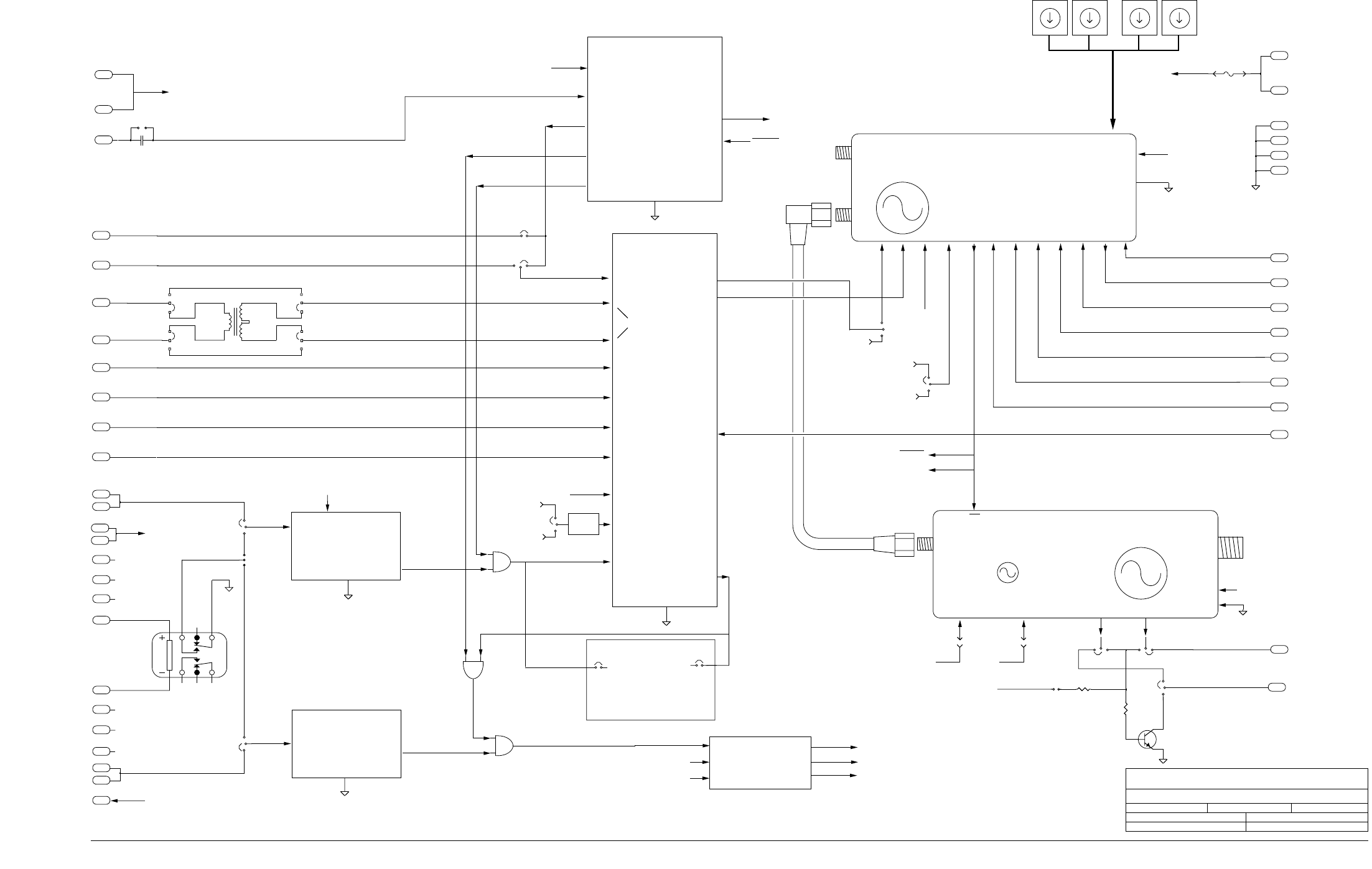
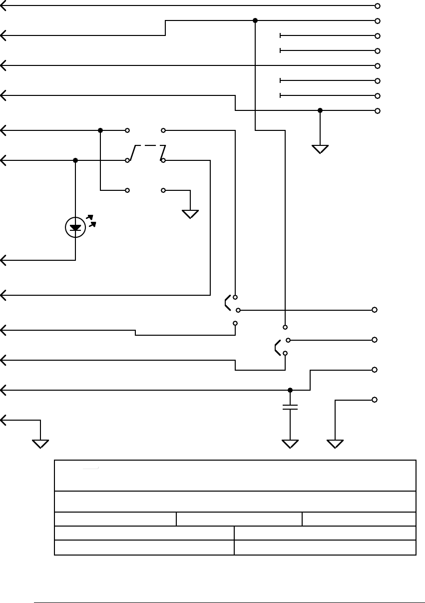
5 ILLUSTRATIONS AND SCHEMATIC DIAGRAMS
5.1 Transmitter Block Diagram
5-1MT-3 AM Transmitter Main Board Instruction Manual
MT-3 TRANSMITTER BLOCK DIAGRAM
SHANE AEBISCHER
43-920917 1.7
19 JULY 1994
9 OCTORBER 1998

DE DANIELS
ELECTRONICS
5-2 MT-3 AM Transmitter Main Board Instruction Manual
This Page Intentionally Left Blank
VICTORIA B.C .
DATE: May 9, 1997
DDANIELS
ELECTRONICS
BOARD No.: 43-920917
DWG REV DATE:
43-920917
DWG No: 9209AS3A
TITLE: MT-3 Component Side SM Layout
Factory installed jumpers
20
19
18
17
16
15
14
13
T1
SPT-196
JS3
JS2
JS1
6
5
4
3
2
1
12
MT-3 FRONT PANEL BOARD
12
11
10
9
8
7
6
5
4
3
2
1
1R0W X 12PIN
1ROW X 9PIN
1ROW X 6PIN
1ROW X 2PIN
RELAY1
OPTIONAL
MT-3 AUDIO PROCESSOR BOARD
3
4
1
2
3
4
1
2
3
4
1
2
3
4
1
2
3
4
1
2
JA1JA2
JA3 JA4 JA5
3
4
1
2
1
2
JF1JF2
ENA
+9.5V
13.8V
FOR
REV
GND
DWG No: TX3AT9D
TITLE: MT-3 Transmitter Component Side T/H Designations
DWG REV DATE:
3
4
JF3
AUDIO IN
C23
100nF
R42
OPT
FSW4
BCD-10
FSW3
BCD-10
FSW2
BCD-10
FSW1
BCD-10 MSD
LSD
- Components Not Installed
12B
SYNTHESIZER GROUND TAB
(Low Power Synthesizer Only)
SYNTHESIZER
GROUND TAB
(Low Power
Synthesizer
Only)
OS-3 RF
OUTPUT
OC-3 RF
OUTPUT
OS-3H ENHANCED SYNTHESIZER
OR
OC-3 CRYSTAL CONTROL MODULE
OST-3H RF
OUTPUT
TP19 TP20
TP22TP21
32
30
28
26
24
22
20
18
16
14
12
10
8
6
4
2
DB Z
TP15 TP16
TP18TP17
TP12 TP13
TP14
TP1 TP2
TP3
TP4
TP5
TP6
TP8
TP9
TP10
TP11
TP7
TP25
TP26
TP27
TP28
TP29
TP30
TP24
TP23
TP33
TP34
TP31
TP32
DE DANIELS
ELECTRONICS
5-5Illustrations and Schematic Diagrams
MT3TXMNM2B
Factory installed jumpers
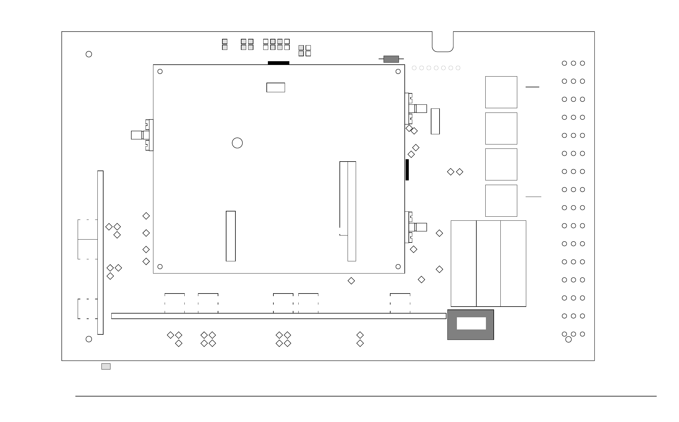
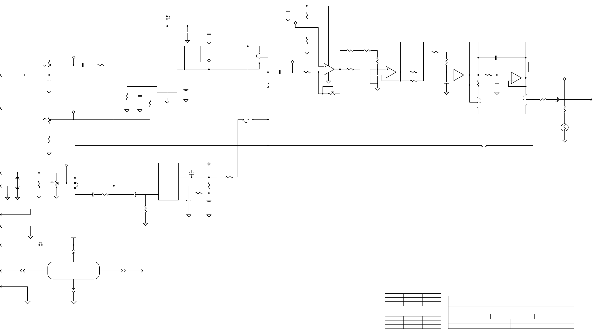
5.2 MT-3 AM Transmitter Board Electrical Assembly
5.2.1 MT-3 AM Transmitter Board Top Side Component Layout
DE DANIELS
ELECTRONICS
5-3MT-3 AM Transmitter Main Board Instruction Manual
VICTORIA B.C .
DATE.: 9 May 1997
DDANIELS
ELECTRONICS
BOARD No.: 43-920917
43-920917
+
+
+
+
+
TITLE: MT-3 Transmitter Solder Side SM Layout
DWG No: 9209AS3B DWG REV DATE: 10 Aug. 1998
+
Factory installed jumpers
Components Not Installed
TITLE: MT-3 Transmitter Solder Side SM Designations
DWG No: 9209AS2D
J18
BYD17J
D4
R2 27k4
D2
BYD17J
R9 221k
R10
100k
R3
1k00
D1
BYD
17J
D3
BYD
17J R6
27k4
R7
1k00 R8
27k4
C6
10nF C5
100nF
U1
33172
10nF C7
100nF C8 R4
27k4 R15
10k0
R18
10k0
U2
4081
R14
10k0 Q1
BC817
BC817
Q3
R12
27k4
R13
27k4
R11
27k4
D6
BYD17J
C3 16V
10µF
C4
1µF
16V
Q9
D15N
06V
Q8
BC807
R24
68k1 R22
68k1
R23
10k0 R21
10K0
R19
10k0
Q4
BC817
R20
68k1
D5
BYD
17J
Q5
D5P06V
Q7
D5P06V
U3
MMAD1108
U4
MMAD1108
C1
10µF
35V
R26
1k00
Q10
PZT
2222
R25
27k4
C2
1µF
35V
Q6
BC817
y
J4
x
J9
J17
y
x
J12
J6
R17
1k00
C12
10nF C13
10nF
LPF35
LPF34
LPF33
LPF32
LPF31
LPF30
LPF29
LPF28
LPF27
LPF26
LPF25
LPF24
LPF23
LPF22
LPF21
LPF20
LPF19
LPF18
LPF17
LPF16
LPF15
LPF12
LPF10
LPF8
LPF3
LPF5
LPF4
LPF2
LPF1
D8
BAS
16
y
J3
x
y
J2
x
x
y
J21
U6
LP
2951
y J7 x
J14
y
R29 82k5
x J13 y
R5
10R0
J16
R110R0 R30
15k0 C15
4.7µF
C14
10nF
D7
BAS
16
M2.5 PRESS NUT
x
LPF14
C10
1 µF
y J25 x
R16
10k0
x
y
x
y
J20 J23
x
y
J19 J22
J24
x J15 y
C20
4.7µF
16V
U8
MC14536B R39
221K
U7
33172 R32
1k00
R34
27k4
R33
68k1 R31
221k
R38
100k
R37
1k00
R36
221k
R35
27k4
C21
100nF C22
100nF
R47
1k00 Q11
BC807-25
R46
221k R43
221k
R44
221k
R45
221k
R41
15K
R40
10K
x
y
R28
DWG REV DATE: 10 Aug. 1998
F1
(3A FUSE OPTIONAL)
CONN1
F/48 MALE
TITLE: MT-3 Transmitter Solder Side T/H Designations
DWG No: TX3AT8D DWG REV DATE: 10 Aug. 1998
M2.5 x 10
PAN/PHIL.
SCREW (2)
Components Not Installed
MT-3 AM AMPLIFIER
GND: BLACK
+ 13.8 VDC: RED
MODULATION INPUT: YELLOW
ENA: BLUE
+ 9.5 VDC: ORANGE
RF IN
BLK
YEL
RED
BLUE
123456
ORG
7
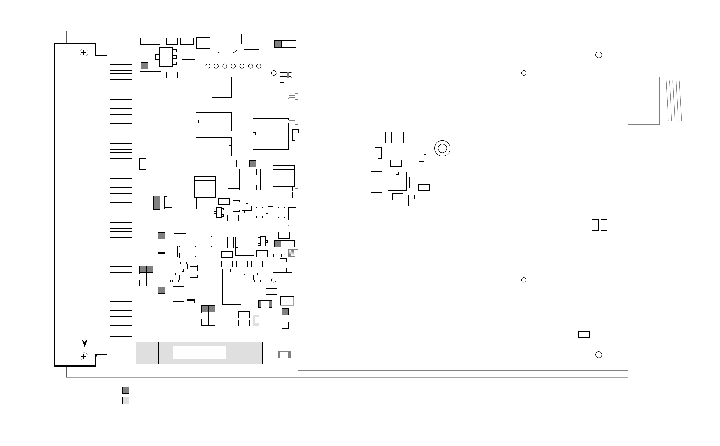
5-4 MT-3 AM Transmitter Main Board Instruction Manual
DE DANIELS
ELECTRONICS
5.2.2 MT-3 AM Transmitter Main Board Component Layout (Bottom)
MT3TXMNM3B
x J15 y
x J13 y
J6
y J25 x
y J7 x
DANIELS
DE ELECTRONICS
J6
J7
InstalledNot Installed
'Y' Position
'X' PositionJ18
Installed Installed
'Y' Position
'X' Position
'X' Position
'X' Position
MODE 1 MODE 2 MODE 3 MODE 4
AM/FM STANDBY MODES STANDARD/LOW FREQUENCY MODULATION
STD MOD VER. LF MOD VER.DESIGN
J6
J7
J18
Installed
'X' Position
'X' Position
Not Installed
'Y' Position
'Y' Position
VICTORIA B.C.
DE DANIELS
ELECTRONICS
Transmitter Main Board Instruction Manual 5-5
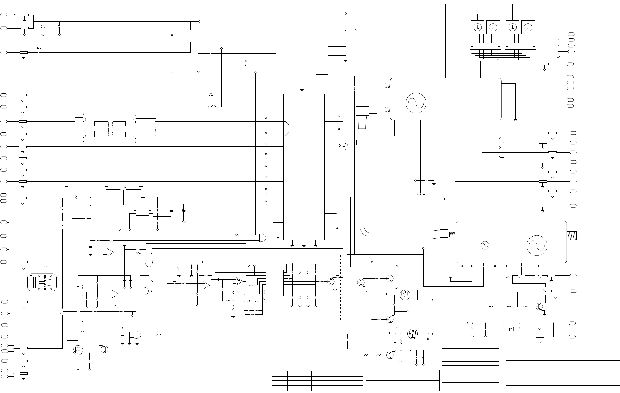
5.2.3 Transmitter Main Board Schematic Diagram
DWG REV DATE: 9 OCTOBER 1998
DWG No.: MT3TXMNM4B
Y
X
NC
NC
NC
MM M
M
LLL
X
BOARD REV: 1.7 BOARD No.: 43-920917
TP34
C23
C17-C19 LPF6,LPF7 LPF11,LPF13
Q2
C9,C11,C16
Q11
R47
U8
J35
U5R27
J10,J11
J1,J5,J8
FSW4
F1
RELAY1
HIGHEST REFERENCE DESIGNATORS
LPF35
T1
D8
----- ----- -----
UNUSED REFERENCE DESIGNATORS
TIME OUT TIMER
APPROX 0.8 VDC
JF3-4
JF3-3
JF3-2
JF3-1
TO
J25 PIN3
TO
JP1-7
X
Y
X
Y
X
Y
X
Y
X
Y
JP1-5JP1-4JP1-6JP1-2JP1-1JP1-3
XY
Y
X
Y
XYX
Y
UNDER U6
X
Y
X
Y
XY
TITLE: MT-3 TRANSMITTER BOARD SCHEMATIC DIAGRAM
JA5-1
JA5-2
JA5-3
JA5-4
JA2-4
JA3-1
JA4-2
JA3-2
JA4-4
JA1-4 JA3-3
JF2-3
JF2-4
JF1-4
JA3-4
JA2-3
JA4-3
JA4-1
JA2-1
JA2-2
JA1-1
JA1-2
JA1-3
APRVD:DWG BY: MIKE GAUBE DATE: 8 APRIL 1992
JF1-1
JF1-3
JF2-2
JF1-2
JF2-1
FRONT PANEL
N CONNECTOR
BACKPLANE
CONNECTOR
LPF
LPF16
LPF
LPF17
LPF
LPF22
LPF
LPF5
LPF
LPF4
LPF
LPF19
LPF
LPF18
LPF
LPF20
LPF
LPF27
LPF
LPF21
LPF
LPF33
LPF
LPF12
LPF
LPF8
LPF
LPF10
LPF
LPF14
LPF
LPF26
LPF
LPF15
Z12
TX STANDBY B12
PTT OUTPUT B24
Z14
PTT NTO B14
NCD4
NCD6
NC
D2
RLY POS B8
NC
D8
NC
D10
NCD12
Z10
PTT WTO B10
DIRECT MOD
INPUT Z28
SQL FLAT
INPUT Z20
SUBTONE
INPUT #2 Z24
SUBTONE
INPUT #1 B22
BALANCED
INPUT #1 Z18
BALANCED
INPUT #2 B18
MIC IN Z4
MIC OUT B4
SQL DE-EMP
INPUT B20
Z6
+9.5V CONTINUOUS
B6
GROUND
B30
GROUND
B32
GROUND
Z32
IMC1
D14
IMC2
D16
IMC3
D18
NC B16
NC Z16
RX MONITOR
B28
RX DATA IN
D30
TX DATA OUT
D28
BOOTSTRAP
D32
CHANNEL SEL 0
(Least Significant Bit)
D20
CHANNEL SEL 1
D22
CHANNEL SEL 2
D24
CHANNEL SEL 3
(Most Significant Bit)
D26
TX AUDIO CONTROL
Z22
VSWR REVERSEZ26
FORWARD POWER
FAIL INDICATOR
B26
+10 TO +17 VOLTS
+13.8 VDC NOMINAL
B2
Z2
LPF
LPF2
LPF
LPF1
LPF
LPF34
LPF
LPF35
LPF
LPF23
LPF
LPF29
LPF
LPF28
LPF
LPF25
LPF
LPF24
LPF
LPF32
LPF
LPF31
LPF
LPF30
10uF
C3 1.0uF
C4
TP5
TP2
TP4
TP3
TP1
10nF
C13
TP6
TO ALL 9.5V SUPPLY POINTS
1.0uF
C10
J9
J16
J17
TP20
TP18
TP22
TP17
TP19
TP21
NOT INSTALLED
R28
9.5V
27K4
R2 BYD17J
D2
BYD17J
D1
J3
1987
43210
RELAY1
J4
BAS16
D7 10R0
R1
27K4
R4
1K0
R3
TP27
2
31
MC33172
aU1
4
5
67
8
MC33172
bU1
BYD17J
D3 27K4
R6
BYD17J
D4
BAS16
D8
10R0
R5 1K0
R7 27K4
R8
TP28
10nF
C6
100K0
R10
221K0
R9
9.5V
9.5V
TP26
89
10
MC14081
cU2
13
12
11
MC14081
dU2
100nF
C8
9.5V
5
6
4
14
7
MC14081
bU2
1
2
3
MC14081
aU2
9.5V
G
D
S
D15N06V
Q9
E
B
C
BC807-25
Q8
10K0
R18
TP11
E
B
C
BC817-25
Q1
E
B
C
BC817-25
Q3
9.5V
9.5V
E
B
C
BC817-25
Q4
BYD17J
D5
BYD17J
D6
J6
TP7
G
DS
D5P06V
Q5
J21
Vin
Error
Sd
Gnd
Vout
Sense
5V Tap
FB
8
5
3
4
1
2
6
7
LP2951
U6
15K0
R30
9.5V
10nF
C14
82K5
R29
4.7uF
C15
J15J13
J14
E
B
C
PZT2222A
Q10
1K0
R26
27K4
R25
J12
9.5V
TO ALL 13.8V SUPPLY POINTS
13.8V
10uF
C1
1.0uF
C2
TP8
TP15
13.8V
TP9
TP16
TP14
1K0
R17
J18
10K0
R16
TP23
TP24
TP10
9.5V
9.5V SWITCHED J7
TO ALL 9.5V SWITCHED
SUPPLY POINTS
TO ALL 9.5V PTT SWITCHED
SUPPLY POINTS
9.5V PTT SWITCHED
9.5V PTT SWITCHED
MICROPHONE INPUT
BALANCED
INPUT
+9.5V
+8.0V SWITCHED
TONE/DIGITAL
INPUT
AUDIO OUTPUT
SUBTONE #1 INPUT
SUBTONE #2 INPUT
DIRECT MODULATION
INPUT
AUDIO
SUBTONE #2
OUTPUT
TOT
INPUT TOT
OUTPUT
GND GND
MT-3 AUDIO
PROCESSOR
13.8 V
QUALIFIED
PTT
PTT
GND
CONTROL
2
1
6
4
5
3
AUDIO XFMR
T1
10nF
C12
27K4
R13
27K4
R12
27K4
R11
10K0
R19
10K0
R15
12
10K0
R14
68K1
R20
10K0
R23
68K1
R24
100nF
C5
10nF
C7
J20
J22
J23
J24
J19
J25
+9.5V INPUT +9.5V OUTPUT
LED ENA
GROUND
MIC PTT WTO
MIC PTT NTO
MIC AUDIO
MT-3 FRONT PANEL BOARD
RX AUDIO SPARE
+13.8V
GROUND
RX MON
13.8V
RF IN RF OUT
+9.5V+13.8V ENA GND FOR REV
OR
MT-3 VHF/UHF AMPLIFIER MODULE
AUDIO
IN
XXXX
LPF
LPF3
F1
OPTIONAL
RLY NEG Z8 68K1
R22
9.5V
E
B
C
BC817-25
Q6
TP30
TP29
G
DS
D5P06V
Q7
10K0
R21
100nF
C22 221k
R39
C23
100nF
221k
R44 221k
R45 221k
R46
221k
R43
15k0
R41
27k4
R35
68k1
R33
221k
R31
1k00
R32
221k
R36
27k4
R34
100k
R38
1k00
R37
OPT
R42
J26
J27
J32
J28
100nF
C21
3
28
4
1
a
MC33172
U7
Q11
BC807-25
SET
RESET
IN1
OUT1
OUT2
BYP
CLK INH
VSS
VDD
MONO
OSC INH
DEC
D
C
B
A
MC14536B
1
2
3
4
5
6
7
8
16
15
14
13
12
11
10
9
U8
TP25
5
67
MC33172
U7b
9.5V
4.7uF
C20
1k00
R47
10k0
R40 J29 J31
J35
J33
J34 TO ALL TOT 9.5V TOT 9.5V
TOT 9.5V
TOT 9.5V
TP12
TP31 TP32
TP13
TP33
TP34
GROUND
Z30
OC-3 CRYSTAL CONTROL MODULE
P1-18 P1-20 P1-12 P1-19 P1-11 P2-2 P1-17 P1-9
P3-2
P3-1
P2-5
P1-10
P1-7
P1-3
P2-3
P1-16P1-8P1-15P1-14P1-6P1-13P1-5P1-4
P1-2 P1-1 P2-1 P2-4 P2-6
RF
OUTPUT
REFERENCE
INPUT
OS-3 SYNTHESIZER
OR
012
3
4
5
6
7
89
MSD
FSW1
13572468
9 11131510121416
U3
MMAD1108 75318642
1513119 16141210
U4
MMAD1108
012
3
4
5
6
7
89
FSW2
012
3
4
5
6
7
89
FSW3
012
3
4
5
6
7
89
LSD
FSW4
9.5V SWITCHED
J2
PTT
TOT INPUT
TOT OUTPUT
QUALIFIED PTT
QUALIFIED PTT
JP1-7
JP1-7
2.2 Vdc
9.4Vdc
2.9 Vdc
2.9Vdc

DE DANIELS
ELECTRONICS
5-6 MT-3 AM Transmitter Main Board Instruction Manual
5. 3 MT-3 Front Panel Board
5.3.1 MT-3 Front Panel Board Component Layout
D1
MIC
12
3
4
PF2
SW1
PF1
+
c b a
f e d
KEYED
NORM
J1
YX
Solder Jumper On Solder Side Of PCB.
Factory Installed Solder Jumper.
MT3TXMNM5A
PF3
J2
Y
X
43-921212
P1
21
43
65
87
1
2
3
4
1
2
3
4
1
2
3
4
DE DANIELS
ELECTRONICS
MT-3 AM Transmitter Main Board Instruction Manual 5-7
5.3.2 MT-3 Front Panel Board Schematic
VICTORIA B.C .
DATE.: DWN:
DWG No:
TITLE:
APRVD:
BOARD NO.: BOARD REV.:
DWG REV DATE:
DE DANIELS
ELECTRONICS
1.2
MT3TXMNM6A 28 MAY 97
07 APRIL 1992
43-921212
MT-3 FRONT PANEL BOARD
M. GAUBE
X
Y
PF3-3
PF3-4
PF3-1
PF3-2
X
PF1-4
PF1-1
PF1-2
PF1-3
PF2-2
PF2-3
PF2-4
PF2-1
MIC-2
MIC-4
MIC-3
MIC-1
Y
KEYED
NORM
D1
J1
C1
N/I
1
2
3
4
MIC
1
2
3
4
PF1
PF2
4
2
1
3
PF3
1
2
3
4
5
6
7
8P1
J2
F
E
D
C
B
A
SW1
+9.5V IN
LED ENA
MIC PTT NTO
MIC PTT WTO
MIC INPUT
MIC INPUT
MIC PTT
MIC PTT
RX MON
RX MON
+9.5V OUT
+9.5V OUT
RX AUDIO
RX AUDIO
+13.8V
+13.8V
SPARESPARE

VICTORIA B.C .
DANIELS
ELECTRONICS
DRAWN BY: SHANE A
DWG REV DATE: AUGUST 24/98
DATE: 24 AUGUST 1998
DWG No: XXXXXAT1
DELECTRONICS
PCB 50049-04
TITLE:TX AM AUDIO PROCESSOR OUTLINE
VICTORIA B.C .
DANIELS
ELECTRONICS
DRAWN BY: SHANE A
DWG REV DATE: AUGUST 24/98
DATE: 24 AUGUST 1998
DWG No: XXXXXAT1
DELECTRONICS
TITLE:TX AM AUDIO PROCESSOR OUTLINE (bottom)
DWG No: VAP130AS1C
TITLE: TX AM AUDIO PROCESSOR LAYOUT
- COMPONENTS NOT INSTALLED
- JUMPERS INSTALLED
DWG REV DATE:AUGUST 25/98
FB 1
C1
4.7nF
R2
20k0
R5
30K9
R6
100k0
C13
1.0nF
R4
50k0
Automatic
Modulation
Control Input
Adjust
R1
5k0
Microphone
Input Level
Adjust
U1
SA571D
C3
680nF
C21
4.7uF
C12
4.7uF
C8
680nF
C9
4.7uF
R26
3M3
C6
100nF
R27
681R0
R16
5k0
Balanced
Input Level
Adjust
R17
10k0
R10
27K4
R11
27K4
C11
2.2uF
R13
18k2
R14
100k0
Modualtion
Control Output
Adjust
R22
3K48
R25
82k5
R9
10k0
U2
MC33174
C23
220pF
C19
1.0uF
R18
470k0
DWG No: VAP130AS2C
TITLE: TX AM AUDIO PROCESSOR SURFACE MOUNT DESIGNATIONS
C7
10nF
JU1
JU8
JU4
X
Y
JU7
DWG REV DATE: MARCH 06 /98
X
Y
JU3
Y
X
JU6
X
Y
JU5
X
Y
C22
680pF
R28
82k5
JU2
C20
220pF
C25
150pF
C17
330pF
R23
51k1
R32
51k1 R31
15k4
R24
15k4
R30
47k5
R20
39k2
R29
5k11
R19
5k11
C18
220pF
R15
49k9
R3
49k9 C14
100nF
JU9
R8
4k75
1
2
3
4
1
2
3
4
1
2
3
4
1
2
3
4
DWG No: VAP130AT1A
TITLE: AM TRANSMITTER THROUGH HOLE LAYOUT
D1
1N5221B
D2
1N5221B
C10
470nF
C5
470nF
C2
470nF
P 3P 2P 5P 1
DWG No: VAP130AT2B
TITLE: AM TRANSMITTER THROUGH HOLE DESIGNATIONS
C15
4.7nF C16
2.2nF
R7
1k2 TEMP
DWG REV DATE: OCTOBER / 98
wo # xxxx
5-8
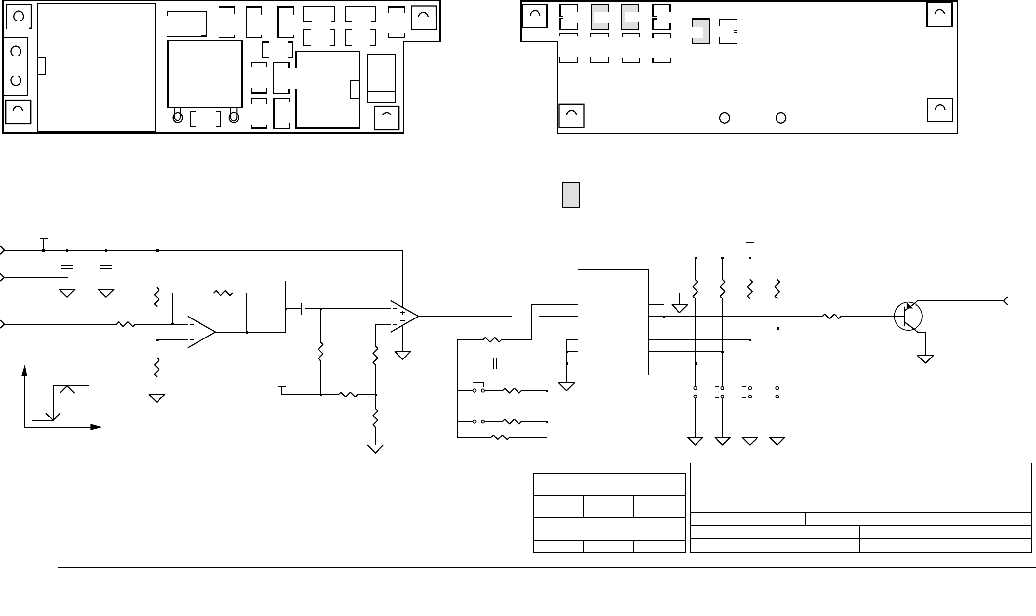
5.4 MT-3 AM Audio Processor Electrical Assembly
5.4.1 MT-3 AM Audio Processor Component Layout
DE DANIELS
ELECTRONICS
MT-3 AM Transmitter Main Board Instruction Manual
TP 6
TP 8
TP 5
TP 4
TP 3
TP2
P 3
P 2 P 5
TP7
P 1
1
2
3
4
1
2
3
4
1
2
3
4
1
2
3
4
P5
P7
P8
P6
Solder Side
Component Side
MT3AMTXM8B
TP1
DE DANIELS
ELECTRONICS
VICTORIA B.C.
DE DANIELS
ELECTRONICS
DWG No: MT3AMTXM9B
TITLE: MT-3 AM Tx AUDIO BOARD SCHEMATIC DIAGRAM
BOARD REV: 04
5.4.2 MT-3 AM Audio Processor Schematic Diagram
MT-3 AM Transmitter Main Board Instruction Manual
JU9
R12, R21C4, C24
ALC Bypass
BOARD No: 50049-04
TP8
Approx. 200mV rms @ 90% mod.
DWG REV DATE: 19 MAY 98
P4
------U2
R32P9
FB1D2C25
3.0 KHZ BUTTERWORTH LOW PASS FIILTER
3.0 KHZ BESSEL LOW PASS FILTER
Y
X
Y
X
YX
Y
X
Y
X
DATE: MARCH 1998
Automatic Level Control
OPTIONAL
5-9
Automatic Modulation Control
DWN BY: STAN POLYAKOV.
13.8 Vdc
9.5 Vdc
Balanced Input
Mod output
AMC Bypass
Modulation Control
Output Adjust
Balanced Input
Level Adjust
Automatic Modulations
Control Input Adjust
Microphone
Microphone Input
Level Adjust
HIGHEST REFERENCE DESIGNATORS
UNUSED REFERENCE DESIGNATORS
APRVD:
FB1
C1
4.7nF
CW
R1
5K0
TP1 C2
470nF
CW
R4
50K0
TP2
Vcc
Rect In
Var G
Rect Cap
Output
Inv In
R3
THD
Trim
GND
2
3
1
7
5
6
8
13
4
aU1
SA571D
Rect In
Var G
Rect Cap
Output
Inv In
R3
THD
Trim
15
14
16
10
12
11
9
bU1
SA571D
R6
100K0
TP3
C3
680nF
C6
100nF C7
10nF
TP4
680nF
C8 4.7uF
C9
470nF
C10 18K2
R13
CW
R16
5K0
C12
4.7uF
C13
1.0nF
470K0
R18
TP5
TP6
C21
4.7uF
TP8
MT-3 TX TIME-OUT-TIMER
3
P1
2
P5
1
P1
2
P1
3
P2
4
P1
4
P3
4
P5
4
P2
1
P3
8.0V
9.5V
8.0V
-1P7
-1P8
-1P9
-1P6
-1J7
-1J8-1J6
-1J5
D1
1N5221B
D2
1N5221B R27
681R0
C11
2.2uF
TP7
R5
30K9
2
P3
2
34
1
11
a
MC33174
U2
6
57
b
MC33174
U2
9
10 8
c
MC33174
U2
8.0V
49K9
R3
49K9
R15
100nF
C14
2.2nF
C16
13
12 14
U2
MC33174
d
R14
100K0
C5
470nF
10K0
R17
4.7nF
C15
51K1
R32
220pF
C18
5K11
R29
5K11
R19
15K4
R24
15K4
R31
51K1
R23
82K5
R28
680pF
C22
220pF
C23
JU5
82K5
R25
JU7
JU8
R20
39K2
R30
47K5
C17
330pF C25
150pF
R2
20K0
C20
220pF
JU6
R22
3K48
JU4
C19
1.0uF
R9
10K0
R10
27K4
R11
27K4
R26
3M30
JU3
JU9
R8
4K75
R7
1K2
JU2
JU1
VICTORIA B.C .
DATE: 15 APRIL 1996
DANIELS
ELECTRONICS
D
BOARD No.: 50027-02
DWG REV DATE:
TITLE: TX AP TIME OUT TIMER COMPONENT SIDE
DWG No: TOTAS
50027-02
INSTALL JUMPERS
VICTORIA B.C .
DATE: 15 APRIL 1996
DANIELS
ELECTRONICS
D
DWG REV DATE:
TITLE: TX AP TIME OUT TIMER COMPONENT SIDE SM LAYOUT
DWG No: TOTAS1
C2
100nF
R6
221k
R8
100k
R5
27k4
R7
1k00
R10
10k0
R3
68k1
C3
100nF
R4
27k4
R1
221k
R2
1k00
U1
MC33172
C1
4.7µF
R11
15k0
R17
1k00
Q1
BC807-25
R9
221k
U2
MC14536B
R12
opt. C4
100nF
J5-1
J7-1
J8-1
J6-1
JU3 JU4 JU5 JU6
JU1 JU2
R13
221k R14
221k R15
221k R16
221k
J5-1
J7-1
J8-1
J6-1
VICTORIA B.C .
DATE: 15 APRIL 1996
DANIELS
ELECTRONICS
D
DWG REV DATE: 2 SEPTEMBER 1997
TITLE: TX AP TIME OUT TIMER COMPONENT SIDESM / TH DESIGNATIONS
DWG No: TOTAS2A
R12
opt. C4
100nF
J5-1
J7-1
J8-1
J6-1
J5-1
J7-1
J8-1
J6-1
VICTORIA B.C.
DE DANIELS
ELECTRONICS
Vin
Vout
9.5V
0V
2.4V
2.0V
2.2VDC
9.4VDC
2.9VDC
0.021VDC 0.135VDC
APPROX 0.8 VDC
2.9VDC
DWN BY: MICHAEL GAUBE APRVD:
+
TITLE: MT-3 TXTIME OUT TIMER SCHEMATIC DIAGRAM
DWG REV DATE: 16 JANUARY 1996
DATE: 19 JANUARY 1996
DWG No: MT3APM4
BOARD No: 50027-02 BOARDREV: VERSION 0.2
-----
HIGHEST REFERENCE DESIGNATORS
----- -----
UNUSED REFERENCE DESIGNATORS
C4 J8 Q1
R17 U2
J1-J4
C3
100nF R9
221k
100nF
C4
R14
221k R15
221k R16
221k
R13
221k
R11
15k0
R10
10k0
R5
27k4
R3
68k1
R1
221k
R2
1k00
R6
221k
R4
27k4
R8
100k
R7
1k00
R12
OPT
R17
1k00
JU1
JU2
JU4 JU5 JU6JU3
+9.5V_CONTINUOUS
+9.5V_CONTINUOUS
C1
4.7uF C2
100nF
SET
RESET
IN1
OUT1
OUT2
BYP
CLK INH
VSS
VDD
MONO
OSC INH
DEC
D
C
B
A
MC14536B
1
2
3
4
5
6
7
8
16
15
14
13
12
11
10
9
U2
+9.5V_CONTINUOUS
5
67
bU1
MC33172
3
2
8
4
1
U1
MC33172
a
1
J6
1J8
BC807-25
Q1
1
J7
1
J5
TOT_I/P_TRIGGER
TOT_O/P_TRIGGER
GND
5-10
5.4.3 TX Time-Out-Timer Electrical Assembly
5.4.3.1 TX Time-Out-Timer Component Layout
DE DANIELS
ELECTRONICS
MT-3 AM Transmitter Main Board Instruction Manual
5.4.3.2 TX Time-Out-Timer Schematic Diagram
MT3APM3 MT3APM5

DE DANIELS
ELECTRONICS
MT-3 AM Transmitter Main Board Instruction Manual 6-1
6 PARTS LISTS
6.1 Transmitter Main Board Parts List
6.1.1 Transmitter Main Board Electrical Parts List
Ref
Design Description
Part
No.
C1 CAP, SM, 10uF TANT, 20%, 35V 1055-6D106K35
C2 CAP, SM, 10uF TANT, 20%, 35V 1055-5B105M35
C3 CAP, SM, 10uF TANT, 20%, 16V 1055-6C106M16
C4 CAP, SM, 10uF TANT, 20%, 16V 1055-5A105M16
C5 CAP, SM, 100nF CER, 0805, X7R 1008-5A104K5R
C6 CAP, SM, 10nF CER 0805 X7R 50V 1008-4A103K5R
C7 CAP, SM, 10nF CER 0805 X7R 50V 1008-4A103K5R
C8 CAP, SM, 100nF CER, 0805, X7R 1008-5A104K5R
C10 CAP, SM, 10uF CER/2225 50 X7R 1008-6H105J5R
C12 CAP, SM, 10nF CER 0805 X7R 50V 1008-4A103K5R
C13 CAP, SM, 10nF CER 0805 X7R 50V 1008-4A103K5R
C14 CAP, SM, 10nF CER 0805 X7R 50V 1008-4A103K5R
C15 CAP, SM, 47uF TANT, 10%, 16V 1055-5B475K16
C20 CAP, SM, 47uF TANT, 10%, 16V 1055-5B475K16
C21 CAP, SM100nF CER,0805,X7R,50V 1008-5A104K5R
C22 CAP, SM100nF CER,0805,X7R,50V 1008-5A104K5R
C23 CAP, 100nF FILM, MMK5, 10%, 63V 1016-5A104K63
D1-D6 DIODE, BYD17J RECTIFIER SOD87 2101-BYD17J00
D7 DIODE, BAS16 SWITCHING, SOT23 2100-BAS16000
D8 DIODE, BAS16 SWITCHING, SOT23 2100-BAS16000
F1 FUSE, 3AMP FAST-BLO, 1-1/4 IN. 5604-5GAGC030
FSW1-4 SWITCH, BCD-10 STEPS,5 PIN,PCB 5273-10BCD001
J30 CONNECTOR, F\48_MALE, R\A_P 3720-6048M0RA
LPF1-35 FILTER, SM, LPF1 EM1\LPF, 360pF F 1306-T361F2D5
Q1 TRANSISTOR, BC817-25 NPN SOT23 2120-BC817025
Q3 TRANSISTOR, BC817-25 NPN SOT23 2120-BC817025
Q4 TRANSISTOR, BC817-25 NPN SOT23 2120-BC817025
Q5 MOSFET, D5P06V P-CHAN., DPAK 2144-D5P06V00
Q6 TRANSISTOR, BC817-25 NPN SOT23 2120-BC817025
Q7 MOSFET, D5P06V P-CHAN., DPAK 2144-D5P06V00
Q8 TRANSISTOR, BC807-25 PNP SOT23 2120-BC807025
Q9 MOSFET, D15N06V N-CHAN., DPAK 2144-D15N06VO
Q10 TRANSISTOR, PZT2222A NPN ST223 2120-PZT2222A
Q11 TRANSISTOR, BC807-25,PNP,SOT23 2120-BC807025
R1 RES., SM, 10R0 0805, 1% 100ppm 1150-1A10R0FP
R2 RES, SM, 27K4 0805, 1% 100ppm 1150-4A2742FP
R3 RES, SM, 1K0 0805, 1% 100ppm 1150-3A1001FP
R4 RES, SM, 27K4 0805, 1% 100ppm 1150-4A2742FP

DE DANIELS
ELECTRONICS
6-2 MT-3 AM Transmitter Main Board Instruction Manual
Ref
Design Description
Part
No
R5 RES, SM, 10R0 0805, 1% 100ppm 1150-1A10R0FP
R6 RES, SM, 27K4 0805, 1% 100ppm 1150-4A2742FP
R7 RES, SM, 1K0 0805, 1% 100ppm 1150-3A1001FP
R8 RES, SM, 27K4 0805, 1% 100ppm 1150-4A2742FP
R9 RES, SM, 221K0 0805, 1% 100ppm 1150-5A2213FP
R10 RES, SM, 100K0 0805, 1% 100ppm 1150-5A1003FP
R11 RES, SM, 27K4 0805, 1% 100ppm 1150-4A2742FP
R12 RES, SM, 27K4 0805, 1% 100ppm 1150-4A2742FP
R13 RES, SM, 27K4 0805, 1% 100ppm 1150-4A2742FP
R14 RES, SM, 10K0 0805, 1% 100ppm 1150-4A1002FP
R15 RES, SM, 10K0 0805, 1% 100ppm 1150-4A1002FP
R16 RES, SM, 10K0 0805, 1% 100ppm 1150-4A1002FP
R17 RES, SM, 1K0 0805, 1% 100ppm 1150-3A1001FP
R18 RES, SM, 10K0 0805, 1% 100ppm 1150-4A1002FP
R19 RES, SM, 10K0 0805, 1% 100ppm 1150-4A1002FP
R20 RES, SM, 68K1 0805, 1% 100ppm 1150-4A6812FP
R21 RES, SM, 10K0 0805, 1% 100ppm 1150-4A1002FP
R22 RES, SM, 68K1 0805, 1% 100ppm 1150-4A6812FP
R23 RES, SM, 10K0 0805, 1% 100ppm 1150-4A1002FP
R24 RES, SM, 68K1 0805, 1% 100ppm 1150-4A6812FP
R25 RES, SM, 27K4 0805, 1% 100ppm 1150-4A2742FP
R26 RES, SM, 1K0 0805, 1% 100ppm 1150-3A1001FP
R28 RES, SM, NOT INSTALLED 0805, 1% 100ppm 1150-4A1502FP
R29 RES, SM, 82K5 0805, 1% 100ppm 1150-4A8252FP
R30 RES, SM, 15K0 0805, 1% 100ppm 1150-4A1502FP
R31 RES, SM221k 0805, 1%, 100ppm 1150-5A2213FP
R32 RES, SM, 1k00 0805, 1%, 100ppm 1150-3A1001FP
R33 RES, SM, 68k1 0805, 1%, 100ppm 1150-4A6812FP
R34 RES, SM, 27k4 0805, 1%, 100ppm 1150-4A2742FP
R35 RES, SM, 27k4 0805, 1%, 100ppm 1150-4A2742FP
R36 RES, SM, 221k 0805, 1%, 100ppm 1150-5A2213FP
R37 RES, SM, 1k00 0805, 1%, 100ppm 1150-3A1001FP
R38 RES, SM, 100k 0805, 1%, 100ppm 1150-5A1003FP
R39 RES, SM, 221k 0805, 1%, 100ppm 1150-5A2213FP
R40 RES, SM, 10k0 0805, 1%, 100ppm 1150-4A1002FP
R41 RES, SM, 15k0 0805, 1%, 100ppm 1150-4A1502FP
R42 RESOPT METAL FILM, 5%,05W OPTIONAL
R43 RES, SM, 221k 0805, 1%, 100ppm 1150-5A2213FP
R44 RES, SM, 221k 0805, 1%, 100ppm 1150-5A2213FP
R45 RES, SM, 221k 0805, 1%, 100ppm 1150-5A2213FP
R46 RES, SM, 221k 0805, 1%, 100ppm 1150-5A2213FP
R47 RES, SM, 1k00 0805, 1%, 100ppm 1150-3A1001FP
RELAY1 RELAY, 9VDC RELAY 9VDC, 2_FORM_C P 5310-2C09P005
T1 TRANSFORMER, AUDIO XFMR AUDIO 600R 1:1 1280-600P6005
U1 IC, MC33172 DUAL_OP_AMP, SO- 2302-33172N08
U2 IC, MC14081 QUAD_2I\P_AND, S 2375-40810N14
U3 IC, MMAD1108 8_DIODE\ARY. SO1 2331-11080N16
U4 IC, MMAD1108 8_DIODE\ARY. SO1 2331-11080N16
U6 IC, LP2951 PROG._VOLT_REG S 2305-29510N08

DE DANIELS
ELECTRONICS
MT-3 AM Transmitter Main Board Instruction Manual 6-3
Ref
Design Description
Part
No.
U7 IC, MC33172 DUAL OP AMP, SO-8 2302-33172N08
U8 IC, MC14536B PROGRAM TIMER, SO-16W 2375-45360W16
6.1.2 Transmitter Main Board Mechanical Parts List
Description Part No. Qty.
CABLE, SMB-SMB PLUG, RG316,12cm $7910-WP0WP012 1 (Crystal Control)
CABLE, SMA-SMB PLUG, RG188,15cm $7910-SP0WP015 1 (Synthesizer)
CABLE, SMA PLUG-PLUG, RG188, 19 cm $7910-SP0SP019 1 (Opt. - Synth only)
CONN, TYPE F 48 MALE, RA, PCB MTG 3720-6048M0RA 1
CONN/RF, SMA JACK-JACK BULKHEAD 5118-J875BJ05 1 (Opt. - Synth only)
CASE, 14HP RF PLUG-IN, MT-3 TX 3802-62502010 1
FASTENER, QUICK RELEASE 3702-10000120 4
GASKET, BeCu,3FINGER,.25",CLIP 5630-12023250 2
HANDLE, FRONT PANEL, 14HP, GREY 3702-10000614 1
HOLE PLUG, 0.25" HOLE, NYLON, BLACK 5671-250N062B 1
LOCKWASHER, M3, SPLIT,A2 STEEL 5814-3M0LK00S 4
MIC CONN, 4 PIN MALE, BLACK 5040-114ST0BK 1
NAMEPLATE, BLANK, 14HP, ALUM. 3702-10001214 1
NUT, M2.5, HEX, 5.0mm, STEEL/Ni 5813-2M5HX50N 2
NUT, M2.5, SQUARE, 5.0mm, ZINC 5813-2M5SQ50Z 2
NUT PRESS, M2.5, 5.6mm OD, PC MNT 5833-T2M55615 1
PANEL/FRNT,W/IDENT:TX-EXTR.VER 3802-61002101 1
PANEL, REAR,POS.4,14HP EXTRSN. 3702-63002101 1
SCREW, M3 x 8, PAN/PHIL, BLACK 5812-3M0PP08T 4
SCREW, M3 x8,OVAL C/S/PHIL,A2 5812-3M0VP08S 4
SCREW, M2.5 X 10, CHEESE/SLOT, A2 5812-2M5CS10S 2
SCREW, M2.5 X 12, FLAT/PHIL, Ni 5812-2M5FP12N 2
SCREW, M3 X 6, OVAL C/S/PHIL, Ni 5812-3M0VP06N 2
SCREW, M3 X 6 PAN/PHIL, A2 5812-3M0PP06S 4
SCREW, M5 X 8 FLAT/PHIL, A2 5812-5M0FP08S 4
TAB, GROUND, MT-3 SYNTH., BRASS 3702-67800905 2 (Synthesizer only)
WIRE, TFE/STRAND., 24AWG, VIOL (13.5 cm) 7121-24S19367 1
WIRE, TFE/STRAND., 24AWG, ORG (12.5 cm) 7121-24S19363 1
WIRE, TFE/STRAND., 24AWG, RED (11.0 cm) 7121-24S19362 1
WIRE, TFE/STRAND., 24AWG, YELLOW (9.5 cm) 7121-24S19364 1

DE DANIELS
ELECTRONICS
6-4 MT-3 AM Transmitter Main Board Instruction Manual
Description Part No. Qty.
WIRE, TFE/STRAND., 24AWG, BLACK (9.0 sm) 7121-24S19360 1
WIRE, TFE/STRAND., 24AWG, BROWN (16.0sm) 7121-24S19361 1
6.1.3 MT-3 Front Panel Board Electrical Parts List
Ref
Desig Description Part No.
D1 LED, RED, 5 mm OD, T-1 3/4 2010-503001RD
PF1 HEADER, 0.1", RA, 2 ROW X 2 PIN 5010-H202RA9T
PF2 HEADER, 0.1", RA, 2 ROW X 2 PIN 5010-H202RA9T
SW1 SWITCH, TOG/DPDT, ON-OFF-ON, PCB/STR 5215-T2031V02
PCB MT-3 TX FRONT PANEL 4321-40921211
6. 2 MT-3 AM Audio Processor Parts List
6.2.1 MT-3 AM Audio Processor Electrical Parts List
Ref
Design Description Part No.
C1 CAP., SM, 4.7nF CER., 1206, X7R 1008-3B472K5R
C2 CAP., 470nF FILM, MMK5,10%,63V 1016-5D474K63
C3 CAP., SM, 680nF TANT., 10%, 35V 1055-4B684K35
C5 CAP., 470nF FILM, MMK5,10%,63V 1016-5D474K63
C6 CAP., SM, 100nF CER., 0805, X7R, 50 1008-5A104K5R
C7 CAP., SM, 10nF CER., 0805, X7R 1008-4B103K5R
C8 CAP., SM, 680nF TANT., 10%, 35V 1055-4B684K35
C9 CAP., SM, 4.7uF TANT., 10%, 16V 1055-5B475K16
C10 CAP., 470nF FILM, MMK5,10%,63V 1016-5D474K63
C11 CAP., SM, 2.2uF TANT., 20%, 20V 1055-5B225K20
C12 CAP., SM, 4.7uF TANT., 10%, 16V 1055-5B475K16
C13 CAP., SM, 1.0nF CER., 0805, X7R, 50V 1008-3A102K5R
C14 CAP., SM, 100nF CER., 0805, X7R, 50V 1008-5A104K5R
C15 CAP., 4.7nF FILM, MMK5, 10%, 63V 1016-3A472K63
C16 CAP., 2.2nF FILM, MMK5, 10%, 63V 1016-3A222K63
C17 CAP., SM, 330pF CER., 0805,C0G 1008-2A331J1G
C18 CAP., SM, 220pF CER., 0805,C0G 1008-2A221J1G
C19 CAP., SM, 1.0uF TANT., 20%, 35V 1055-5B105M35
C20 CAP., SM, 220pF CER., 0805,C0G 1008-2A221J1G
C21 CAP., SM, 4.7uF TANT., 10%, 16V 1055-5B475K16
C22 CAP., SM, 680pF CER., 1206,C0G 1008-2B681J1G
C23 CAP., SM, 220pF CER., 0805,C0G 1008-2A221J1G
C25 CAP., SM, 150pF CER., 0805,C0G 1008-2A151J1G
D1 DIODE, 1N5221B ZENER 3.9V,DO35 2002-1N5221B0
D2 DIODE, 1N5221B ZENER 3.9V,DO35 2002-1N5221B0
FB1 FERRITE BEAD, SM,FERRITE BEAD 43MIX,.18x.12 1213-43181200

DE DANIELS
ELECTRONICS
MT-3 AM Transmitter Main Board Instruction Manual 6-5
Ref
Design Description Part No
P1-P5 HEADER 01", R/A, 2 ROW X 2PIN 5010-H202RA9T
PCB AUDIO PROCESSOR, VT-3A130 4322-30500494
R1 POT., SM, 5K0 4mm SQ, 11T,SIDE 1174-DM2502J0
R2 RES., SM, 20K0 0805, 1%,100ppm 1150-4A2002FP
R3 RES., SM, 49K9 0805, 1%,100ppm 1150-4A4992FP
R4 POT., SM, 50K0 4mm SQ, 50K, 11T,SIDE 1174-DM3503J0
R5 RES., SM, 30K9 0805, 1%,100ppm 1150-4A3092FP
R6 RES., SM, 100K0 0805, 1%,100ppm 1150-5A1003FP
R7 TEMPSISTOR, 1K2 PTC, 10%,AXIAL 1181-3AGD122K
R8 RES., SM, 4K75 0805, 1%,100ppm 1150-3A4751FP
R9 RES., SM, 10K0 0805, 1%,100ppm 1150-4A1002FP
R10 RES., SM, 27K4 0805, 1%,100ppm 1150-4A2742FP
R11 RES., SM, 27K4 0805, 1%,100ppm 1150-4A2742FP
R13 RES., SM, 18K2 0805, 1%,100ppm 1150-4A1822FP
R14 POT., SM, 100K0 4mm SQ, 100K,11T,SIDE 1174-DM4104J0
R15 RES., SM, 49K9 0805, 1%,100ppm 1150-4A4992FP
R16 POT., SM, 5K0 4mm SQ, 11T,SIDE 1174-DM2502J0
R17 RES., SM, 10K0 0805, 1%,100ppm 1150-4A1002FP
R18 RES., SM, 470K0 0805, 1%,100ppm 1150-5A4703FP
R19 RES., SM, 5K11 0805, 1%,100ppm 1150-3A5111FP
R20 RES., SM, 39K2 0805, 1%,100ppm 1150-4A3922FP
R22 RES., SM, 3K48 0805, 1%,100ppm 1150-3A3481FP
R23 RES., SM, 51K1 0805, 1%,100ppm 1150-4A5112FP
R24 RES., SM, 15K4 0805, 1%,100ppm 1150-4A1542FP
R25 RES., SM, 82K5 1206, 1%,100ppm 1150-4B8252FP
R26 RES., SM, 3M30 0805, 5%,200ppm 1150-6A3304JL
R27 RES., SM, 681R0 0805, 1%,100ppm 1150-2A6810FP
R28 RES., SM, 82K5 1206, 1%,100ppm 1150-4B8252FP
R29 RES., SM, 5K11 0805, 1%,100ppm 1150-3A5111FP
R30 RES., SM, 47K5 0805, 1%,100ppm 1150-4A4752FP
R31 RES., SM, 15K4 0805, 1%,100ppm 1150-4A1542FP
R32 RES., SM, 51K1 0805, 1%,100ppm 1150-4A5112FP
U1 IC, SA571D COMPANDOR, SO-16L 2327-SA571D00
U2 IC, MC33174 QUAD OP AMP,SO-14 2304-33174N14

DE DANIELS
ELECTRONICS
6-6 MT-3 AM Transmitter Main Board Instruction Manual
This page intentionally left blank.

DE DANIELS
ELECTRONICS
MT-3 AM Transmitter Main Board Instruction Manual 7-1
7 REVISION HISTORY
ISSUE DATE REVISION
1 May 97 •First Issue.
2 March 98 •To improve performance and efficiency of the Audio Processor Board.
ECO #541.
- C18 was 82pF is now 150pF
- R20 was 8k25 is now 3k01
- R21 was 1M0 is now not installed
- R26 was 470k is now 3M30
- Moved SM jumpers to the SM side of the PCB. Moved P1, P2 & P5
to the correct positions. Added land pattern to the PCB for R21.
3 June 98 •Corrected the part number for D1 and D2 on the MT-3 AM Audio
Processor Electrical Parts List.
December 98 •The Butterworth filter stages were changed to Bessel filters to improve
the differetnial group delay of the AM Transmitter. ECO #563.
- The AM Audio Processor PCB was 50049-02 is now 50049-04.
•Updated the DE logo and added the statutary notice to the title page.
Corrected the drawing numbers on the Transmitter layout and schematic
drawing.

DE DANIELS
ELECTRONICS
7-2 MT-3 AM Transmitter Main Board Instruction Manual
This page intentionally left blank.