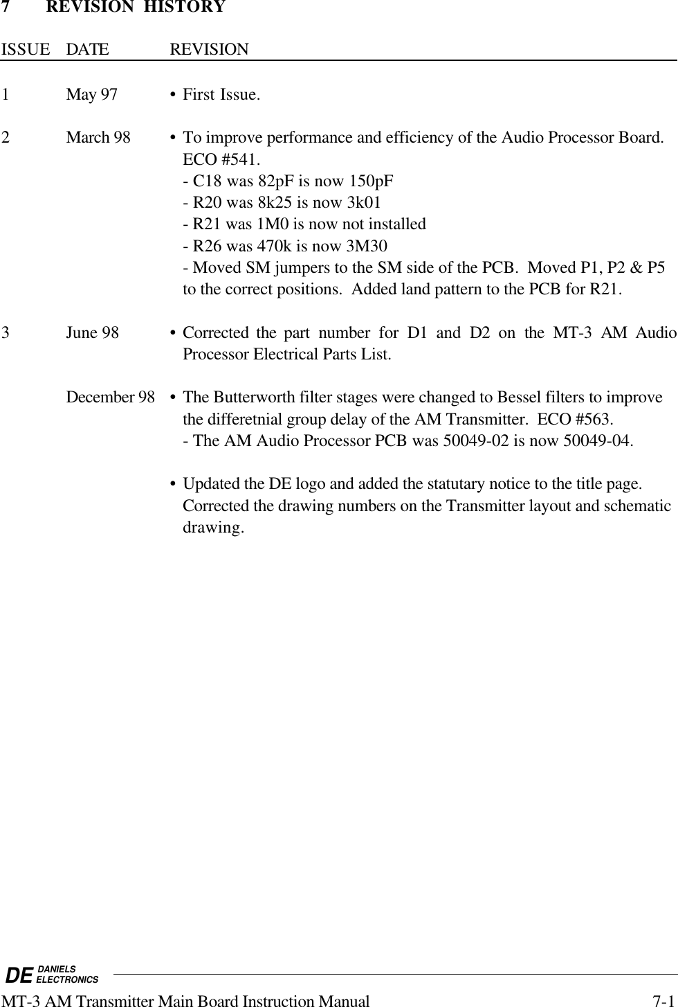
Codan Radio Communications VT-3A130-S-FSH Transmitter User Manual MT 3 AM Transmitter Main Board Instruction Manual

Codan Radio Communications Transmitter MT 3 AM Transmitter Main Board Instruction Manual

MT 3 AM Transmitter Main Board Instruction Manual

DANIELSELECTRONICS LTD.TMMT-3 RADIO SYSTEMSMT-3 AM TRANSMITTERMAIN BOARDINSTRUCTION MANUALCovers:A22-VAP130 AM Audio Processor Version 04                    A21-TX3-00 TXMAIN/FPB Common Asembly Version 1.7Copyright © 1998 Daniels Electronics Ltd.  All rights reserved.  No part of this publication may bereproduced, stored in a retrieval system or transmitted in any form or by any means,  electronic,mechanical, photocopying, recording or otherwise, without the  prior written consent of DanielsElectronics Ltd.DE™ is a registered trademark of Daniels Electronics Ltd.  registered in the United States Patentand Trademark Office.Issue: 3 Previous Issue: 2Issue Date: December 98 Previous Issue Date: March 98 Daniels Electronics Ltd.Printing Date: N/A Victoria, BCPart No.: IM22-MT3AMTXMN PRINTED IN CANADA
DE DANIELSELECTRONICSii MT-3 AM Transmitter Main Board Instruction ManualReviewed By:Quality Assurance:Larry        Freeman                                                                                         _________________Name Signature DateNOTE:The user's authority to operate this equipment could be revoked through anychanges or modifications not expressly approved by Daniels Electronics Ltd.The design of this equipment is subject to change due to continuousdevelopment.  This equipment may incorporate minor changes in detail from theinformation contained in this manual.
DE DANIELSELECTRONICSMT-3 AM Transmitter Main Board Instruction Manual iiiTABLE OF CONTENTSPage1 GENERAL......................................................................................1-11.1 Introduction...........................................................................1-11.2 Performance Specifications .........................................................1-11.2.1 General .......................................................................1-11.2.2 Audio Specifications........................................................1-22 THEORY OF OPERATION ..................................................................2-12.1 MT-3 AM Transmitter Main Board ................................................2-12.1.1 General .......................................................................2-12.1.2 Transmitter Push-To-Talk..................................................2-12.1.2.1 Microphone PTT ...................................................2-12.1.2.2 PTT With Time-Out-Timer........................................2-22.1.2.3 PTT No Time-Out-Timer..........................................2-22.1.2.4 Optional Relay......................................................2-22.1.2.5 PTT Output .........................................................2-32.1.2.6 PTT Voltage Switching............................................2-32.1.2.7 Transmitter Standby Modes.......................................2-32.1.3 Audio Circuits...............................................................2-42.1.3.1 Microphone Audio .................................................2-52.1.3.2 Received Audio.....................................................2-52.1.4 Channel Selection ...........................................................2-52.1.4.1 Synthesized Transmitter...........................................2-52.1.4.2 Crystal Controlled Transmitter ...................................2-52.1.5 Amplifier Circuits ...........................................................2-62.2 MT-3 Front Panel Board ............................................................2-62.3 MT-3 AM Audio Processor.........................................................2-62.3.1 General .......................................................................2-62.3.2 Power Requirements........................................................2-62.3.3 Audio Circuitry..............................................................2-72.3.4 PTT Time-Out-Timer .......................................................2-83 TRANSMITTER ALIGNMENT.............................................................3-13.1 General ................................................................................3-13.2 Repair Note ...........................................................................3-13.3 Printed Circuitboard Numbering Convention.....................................3-13.4 Recommended Test Equipment List ...............................................3-13.5 Standard Factory Settings and Jumper Configuration ...........................3-23.5.1 MT-3 AM Transmitter Board Factory Configuration ...................3-23.5.2 MT-3 AM Audio Processor Factory Configuration.....................3-33.6 MT-3 AM Transmitter Board Alignment ..........................................3-3
DE DANIELSELECTRONICSiv MT-3 AM Transmitter Main Board Instruction Manual3.6.1 General....................................................................... 3-33.6.2 MT-3 AM Transmitter Board Test Points................................ 3-43.7 Module Installation and Removal.................................................. 3-43.8 MT-3 AM Audio Processor Alignment ........................................... 3-53.8.1 General....................................................................... 3-53.8.2 MT-3 AM  Audio Processor Adjustment ................................ 3-54 TRANSMITTER INTERCONNECT PIN DEFINITIONS.............................. 4-15 ILLUSTRATIONS AND SCHEMATIC DIAGRAMS ................................... 5-15.1 MT-3 AM Transmitter Block Diagram ............................................ 5-15.2 MT-3 AM Transmitter Board Electrical Assembly............................... 5-35.2.1 MT-3 AM Transmitter Main Board Component Layout (Top)........ 5-35.2.2 MT-3 AM Transmitter Main Board  Component Layout (Bottom) ... 5-45.2.3 MT-3 AM Transmitter Main Board Schematic Diagram ............... 5-55.3 MT-3 Front Panel Board............................................................ 5-65.3.1 MT-3 Front Panel Board Component Layout ........................... 5-65.3.2 MT-3 Front Panel Board Schematic...................................... 5-75.4 MT-3 AM Audio Processor Electrical Assembly ................................ 5-85.4.1 MT-3 AM Audio Processor Component Layout........................ 5-85.4.2 MT-3 AM Audio Processor Schematic Diagram........................ 5-96 PARTS LISTS................................................................................. 6-16.1 Transmitter Main Board Parts List................................................. 6-16.1.1 Transmitter Main Board Electrical Parts List ............................ 6-16.1.2 Transmitter Main Board Mechanical Parts List.......................... 6-36.1.3 MT-3 Front Panel Board Electrical Parts List ........................... 6-46.2 MT-3 AM Audio Processor Parts List ............................................ 6-46.2.1 MT-3 AM Audio Processor Electrical Parts List........................ 6-47 REVISION HISTORY........................................................................ 7-1
DE DANIELSELECTRONICSMT-3 AM Transmitter Main Board Instruction Manual 1-11 GENERAL1.1 IntroductionThe MT-3 AM Transmitter Main Board integrates the MT-3 Front Panel Board, MT-3 AM AudioProcessor,  Synthesizer or Crystal Control module and Amplifier module together to make aworking MT-3 AM series transmitter (see section 5.1: MT-3 AM Transmitter Block Diagram). TheFront Panel Board and the Audio Processor are soldered  directly to the Transmitter Main Boardwhile the Amplifier and the Synthesizer or Crystal Control module are frequency band sensitive,plug-in modules. Circuitry and jumpers on the Transmitter Main Board control the operation of themodules as well as the overall operation of the MT-3 transmitter. Power and signal connections aremade to the 48 pin type 'F' connector on the rear of the Transmitter Main Board and are routed tothe other modules.  The front and rear back plates are attached to the Transmitter Main Board andtogether with the extruded aluminum shell, as discussed in the assembly section of the TransmitterManual, form the transmitter enclosure.1.2 Performance Specifications1.2.1 GeneralType: MT-3 AM Series TransmitterCompatibility: VT-3A Series Amplifier, OCT-3 Crystal Oscillator,  OST-3Frequency Synthesizer.Modulation: 6K00A3 (Amplitude Modulation)Operating Temperature Range: -30˚C to +60˚C, optional - 40˚C temperature test.Operating Humidity: 95% RH (non-condensing) at +25°C.Operating Voltage: +13.8Vdc , +9.5 Vdc Regulated.Front Panel Control: One 3 position switch• NORM (repeat mode)• OFF• KEY TXPTT Activation: • Active to ground with or without time-out-timer;• Microphone activated with or without time-out-timer;• Front Panel switch: KEY TX - without time-out-timer;• NORM - with or without time-out-timer.• Isolated (optional relay) with or without time-out-timer.PTT Time-Out-Timer: Selectable from 1 sec. to 8 hrs. (factory set 5 min.).
DE DANIELSELECTRONICS1-2 MT-3 AM Transmitter Main Board Instruction Manual1.2.2 Audio SpecificationsAudio Input: -30 to 0 dBm into a 600Ω balanced load.Audio Response: Flat audio; +1/-3 dB:  300 Hz - 3 kHzAudio Distortion: Less than 3% -40˚C to +60˚C at 30% modulationLess than 5% -40˚C to +60˚C at 90% modulation
DE DANIELSELECTRONICSMT-3 AM Transmitter Main Board Instruction Manual 2-12 THEORY OF OPERATION2.1 MT-3 AM Transmitter Main Board2.1.1 GeneralSwitch SW1 on the  Front  Panel Board is a DPDT  switch which controls the operation of thetransmitter as discussed in the operations section of the Transmitter Manual. When SW1 is in the'OFF' position the transmitter is turned off; however, +13.8 Vdc is still present on the TransmitterMain Board as the +13.8 Vdc supply is not switched.  When SW1 is in the  'KEYED' position,+9.5  Vdc is supplied to the transmitter circuitry and the transmitter is continuously turned on.When SW1 is in the 'NORM'  position, +9.5 Vdc is supplied to the transmitter circuitry and thetransmitter can be keyed from several Push-To-Talk inputs.Refer to section 5.2.3  Transmitter Main Board Schematic Diagram".2.1.2 Transmitter Push-To-TalkAll three of the Push-To-Talk (PTT) inputs that key the transmitter are active low (< +2.0  Vdc).One PTT input is on the front panel microphone connector.  The other two PTT inputs: PTT WTO(PTT With Time-Out-Timer) and PTT NTO (PTT No Time-Out-Timer), are on the backplaneconnector of the transmitter board.  If required, the microphone's PTT input can be configured toactivate the transmitter's Time-Out-Timer (TOT).  An isolated PTT input can be made available byinstalling an optional relay (RELAY1) and configuring jumpers J2 to J4 so that the relay controlsthe PTT circuitry.2.1.2.1 Microphone PTTJumper J1 on the MT-3 Front Panel Board configures the microphone's PTT input (MIC PTT) toeither bypass or activate the transmitter's TOT.  Soldering jumper J1 in the 'x'  position (default)selects the MIC PTT NTO line which bypasses the TOT.  Soldering J1 to the 'y'  position selectsthe MIC PTT WTO line which activates the transmitter's TOT.  When  SW1 is in the 'KEYED'position the MIC PTT NTO line is automatically grounded.  Refer to Section 5.3.1, "MT-3 FrontPanel Board Component Layout" for the location of jumper J1.
DE DANIELSELECTRONICS2-2 MT-3 AM Transmitter Main Board Instruction Manual2.1.2.2 PTT With Time-Out-TimerPins B10 and Z10 of the backplane connector are the PTT WTO input.  When the PTT WTOsignal, which is normally high, falls below +2.0 Vdc, the transmitter is keyed.  The transmitter isdisabled  when  the PTT WTO  input  rises  above  +2.3  Vdc or if the TOT's time-out period isexceeded.  If the time-out period is exceeded the PTT WTO input must go high (>+2.3  Vdc) andthen low again in order to rekey the transmitter.The PTT WTO threshold of approximately +2 Vdc (0.3  Vdc hysteresis) is set by U1a, R1, R2,R3, R4, R9, and R10 while diodes D1 and D2 provide overvoltage protection for U1a.  The PTTWTO signal output  from U1a is 'AND'ed with the MIC PTT WTO by U2a.  When either the PTTWTO or the MIC PTT WTO is activated the output of U2a goes low which triggers thetransmitter's TOT located on the MT-3 Audio Processor.  The TOT's output is 'AND'ed  with theMIC PTT NTO signal (U2c) and the PTT NTO signal (U2d).  When any one of the precedingthree signals (TOT's output, MIC PTT NTO,  PTT NTO) go low  the transmitter is activated bytransistors Q1 to Q7 which switch power to the various modules.2.1.2.3 PTT No Time-Out-TimerPins B14 and Z14 of the backplane connector are the PTT NTO input.  When the PTT NTO signal,which is normally high, falls below +2.0 Vdc, the transmitter is keyed.  As long as the PTT NTOsignal remains below +2.0 Vdc the transmitter will remain keyed.  The transmitter is disabled whenthe PTT NTO signal rises above +2.3 Vdc.The PTT NTO threshold of approximately +2 Vdc (0.3 Vdc hysteresis) is set by U1b, R5, R6,R7, R8, R9, and R10 while diodes D3 and D4 provide overvoltage protection for U1b.  The PTTNTO signal is 'AND'ed  with the output of U2c (MIC PTT NTO signal 'AND'ed  with  the TOToutput) by U2d.  When the output of U2d goes low the transmitter is activated by transistors Q1 toQ7 which switch power to the various modules.2.1.2.4 Optional RelayThe transmitter's PTT circuitry can be completely isolated by installing RELAY1.  Jumpers J2 toJ4 configure the relay to provide an isolated PTT input for either the PTT WTO line or PTT NTOline.  The isolated PTT input is enabled by energizing the relay.  The transmitter board will acceptany of the Aromat TF2E line relays.  These relays are  DPDT, single side stable, and have  coilvoltages ranging from +3 Vdc to +48 Vdc.  Only one set of relay contacts are used to activate thePTT circuitry, the other set of contacts are brought out to the backplane connector.To configure the isolated input for PTT WTO operation jumpers J2, J4 must be in the 'y'position,J3  must be in the 'x'  position.  In this mode, pins B10 and Z10 no longer function as the PTTWTO input; however, pins B14 and Z14 continue to function as the normal PTT NTO input.
DE DANIELSELECTRONICSMT-3 AM Transmitter Main Board Instruction Manual 2-3To configure the isolated input for PTT NTO operation jumpers J2, J4, must be in the 'x'  positionJ3 must be in the 'y' position. In this mode, pins B14 and Z14 no longer function as the PTT NTOinput; however, pins B10 and Z10 continue to function as the normal PTT WTO input.2.1.2.5 PTT OutputPin B24 on the backplane connector is an open drain output (Q9) which is pulled low anytime thetransmitter is keyed and the synthesizer is locked.  A crystal controlled transmitter does not have alocked condition so pin B24 is pulled  low  anytime the transmitter is keyed.  Q9, an N-channelMOSFET capable of sinking currents up to 2 Amps, is activated by Q8 which is activated by theQualified PTT signal (JS2-6) of the  synthesizer or crystal control module.  The Qualified PTTsignal also controls the LED ENA line for diode D1 on the front panel board and enable line for theVT-3A   Amplifier Module (JP1-1).2.1.2.6 PTT Voltage SwitchingThe PTT voltage switching circuitry is comprised of transistors Q1 through Q7 and the associatedresistors.  The base of Q1 is driven by the output of U2d which is the combined PTT signal fromall of the PTT inputs.  When the transmitter is keyed, Q1 is turned off and subsequently transistorsQ3, Q4, and Q6 are turned on.  Transistors Q3, Q4, and Q6 provide three different functions:•Q3 provides the active low signal for the synthesizer or crystal module PTT input;•Q4 turns on Q5 which turns on the +9.5 Vdc Switched supply;•Q6 turns on Q7 which turns on the +9.5 Vdc PTT Switched supply.The '+9.5 Vdc Switched' supply (Q5) can also be activated by installing jumper J6 or by externallygrounding the TX Standby Line (pins B12 and Z12).  The '+9.5  Vdc PTT Switched' supply andthe '+9.5 Vdc Switched' supply both provide +9.5 Vdc but depending on how jumpers J6,  J7 andJ18 are configured the transmitter's standby mode will change.2.1.2.7 Transmitter Standby ModesThe VT-3A130 Transmitter has four different standby modes that trade-off standby currentconsumption for start-up speed.  The standby modes are determined by three jumpers: jumper J6which always turns on the '+9.5 Vdc Switched' supply, jumper J7 which selects the power sourcefor the MT-3 AM Audio Processor  and jumper J18 which selects the enable line for  the OST-3A128 Synthesizer or OCT-3 Crystal Control Module.  The actual current and start-up time may depend on the frequncy controlled source (crystal orsynthesizer) and amplifier module.  The current and start-up times given below are representativevalues intended only as a guideline.
DE DANIELSELECTRONICS2-4 MT-3 AM Transmitter Main Board Instruction Manual•MODE 1:Jumper J6 out- the audio processor is switched by a PTT signal- the synthesizer or crystal module is  switched by a PTT signal- standby current: Synthesized - typically 13 mACrystal Controlled - typically 6 mA- start-up time: Synthesized - typically 40 msCrystal Controlled - typically 40 ms•MODE 2:Jumper J6 in, jumper J7 in the 'y' position, jumper J18 in the 'x' position- the audio processor is switched by a PTT signal- the synthesizer or crystal module is enabled all of the time- standby current: Synthesized - not used in this modeCrystal Controlled - typically  6 mA- start-up time: Synthesized - not used in this modeCrystal Controlled - typically   40 ms          • MODE 3:Jumper J6 in, jumper J7 in the 'x' position, jumper J18 in the 'y' position- the audio processor is enabled all of the time- the synthesizer or  crystal module is  switched by a PTT signal- standby current: Synthesized - typically 19 mACrystal Controlled - typically 11 mA- start-up time: Synthesized - typically 40 msCrystal Controlled - typically 8 ms•MODE 4:Jumper J6 in, jumper J7 in the 'x' position, jumper J18 in the 'x' position- the audio processor is enabled all of the time- the synthesizer or crystal module is enabled all of the time- standby current: Synthesized - typically 163 mACrystal Controlled - typically 23 mA- start-up time: Synthesized - typically 12 msCrystal Controlled - typically 8 ms2.1.3 Audio CircuitsAll of the audio signal conditioning (e.g.  limiting, filtering) is performed by the MT-3 AM AudioProcessor.  The transmitter board routes the audio lines from the backplane connector to the audioprocessor. The audio lines routed to the audio processor are:  a 600 ohm balanced input (pins B18and Z18), and a MIC AUDIO from the MT-3 FRONT PANEL BOARD.   It is here that the MICaudio is processed in the same manner as the 600 ohm balanced audio.The audio processor's balanced input pins are isolated from pins B18 and Z18 by a transformer(T1).  Two audio outputs from the MT-3 AM Audio Processor  are routed to the VT-3A130Amplifier.
DE DANIELSELECTRONICSMT-3 AM Transmitter Main Board Instruction Manual 2-52.1.3.1 Microphone AudioNormally the audio from a transmitter's microphone is transmitted by that transmitter; however, theTransmitter Main Board can be configured by the MIC IN and MIC OUT lines so that the audiofrom an external microphone modulates transmitter.  The configuration of the MIC IN (pin Z4) andMIC OUT (pin B4) lines on the MT-3 Transmitter Board are controlled by jumpers J16  and J17respectively.  Jumper J16 selects the audio source for the MT-3 AM Audio Processor'smicrophone input.  Jumper J17 is used to enable or disable the MIC OUT line.  Normally thetransmitter's microphone is selected (J16 in the 'x' position) and the MIC OUT line is enabled (J17is installed).2.1.3.2 Received AudioPin B20 is the audio input from the transmitter's corresponding receiver.  The default setting forthis line is to have it AC coupled (Jumper J9 is out) and directly connected to the front panel boardRX AUDIO line.2.1.4 Channel Selection2.1.4.1 Synthesized TransmitterEight backplane connections are used to communicate with the synthesizer unit.  Pins D28, D30,and D32 are used (in house) to program the  synthesizer.  Channel select lines (pins D20, D22,D24, and D26) are used once the synthesizer is programmed to select one of 16 channels.  If thechannel select lines are all low (channel 0) the channel for the  synthesizer is read from switchesFSW1 (most significant), FSW2, FSW3, and  FSW4  (least significant).  Since the resultingfrequency is dependent on the transmitter model, refer to the section on frequency selection in theTransmitter Manual or to the channel designation tables for that particular transmitter.2.1.4.2 Crystal Controlled TransmitterThe crystal control module is a direct replacement for the synthesizer module and therefore uses thesame connections as the synthesizer to connects to the MT-3 AM Transmitter Main  Board.  Thechannel select lines and switches FSW1 to FSW4 are not used by the crystal control module as thetransmitter's operating frequency is determined by the crystal control module's crystal frequency.A frequency multiplication  factor, described in the manual for this module, relates the crystalfrequency to the operating frequency .
DE DANIELSELECTRONICS2-6 MT-3 AM Transmitter Main Board Instruction Manual2.1.5 Amplifier CircuitsThe MT-3A series  Amplifier  has 5 connections that are cabled to the transmitter board: +13.8Vdc, +9.5 Vdc, Enable, Mod and Gnd.  The +13.8 Vdc supply (JP1-3) is always on while the+9.5 Vdc supply (JP1-2) is always switched by a PTT signal.  The enable line (JP1-1) is activelow and is controlled by the Qualified PTT signal from the synthesizer.Jumpers J12, J13, J14, and J15 are not installed.2. 2 MT-3 Front Panel BoardThe MT-3 Front Panel Board is a subsection of the MT-3 AM Transmitter Board which is used tomount the front panel switch, diode, and microphone connector.  The main purpose of the board isto eliminate a wiring harness for the front panel components.  Jumper J1, located on the rear of thecircuitboard, is used to select whether or not the MIC PTT line activates the transmitter's TOT:•Jumper J1: 'x' position MIC PTT NTO   no time-out-timer (factory setting)'y' position MIC PTT WTO  with time-out-timerRefer to section 5.3.2 "MT-3 Front Panel Board Schematic Diagram".2.3 MT-3 AM Audio Processor2.3.1 GeneralThe MT-3 AM  Audio Processor is a versatile circuitboard that can provide several types of audioprocessing.  The module also has an on-board programmable push-to-talk (PTT) time-out-timer(TOT) on an attached circuitboard.  A continuous +9.5  Vdc supply and a continuous +13.8 Vdcsupply together with a switched +8.0  Vdc  supply  are required to power  the  module.  Refer tosection 5.4.1 "MT-3 AM Audio Processor Component Layout" and to section 5.4.2 "MT-3 AMAudio Processor Schematic Diagram" for component location and designation references.2.3.2 Power RequirementsThe audio processor can be configured for continuous audio standby or for switched audio standbyby the Transmitter Main Board.  If fast audio risetime is desired, the transmitter should be operatedin standby mode 3 or 4 as specified in section 2.1.2.7.  The current for  the associated TOT isapproximately 4 mA when the transmitter is keyed.
DE DANIELSELECTRONICSMT-3 AM Transmitter Main Board Instruction Manual 2-72.3.3 Audio CircuitryThe MT-3 AM Tx  Audio Processor refer to section 5.4.2 "MT-3 AM Audio Processor SchematicDiagram"  has two audio inputs (Microphone input and Balanced input) which  can be used tomodulate the transmitter.   The input signals  are combined  by R2 and R17 at a compandor  U1.U1b controls the input level and makes gain inversely proportional to the input level (say a 20 dBdrop in input  level will produced a 20 dB increase in gain). The output will remain fixed at aconstant level without clipping and distortion.  (Automatic Level Control)  The input signals areadjusted by the pots R1, R16. The variable gain cell in U1a  is used as a voltage-controlledamplifier so that if the power supply (13.8Vdc)  has changed the output level will change in orderto keep the modulation  of the RF output signal  at the same level. The gain control can be adjust bythe  pot  R4. (Automatic Modulation Control) The audio signal then amplifies and filters at  U2.The output signal is adjusted by the pot R9.
DE DANIELSELECTRONICS2-8 MT-3 AM Transmitter Main Board Instruction Manual2.3.4 PTT Time-Out-TimerThe PTT time-out-timer (TOT) is a relatively independent circuitry located on the TransmitterBoard.  The TOT is powered from the continuous +9.5 Vdc supply (J34) and is programmable forvarious time-out periods.  The TOT input  is normally high and in this state the timer is disabled.When the input trigger level falls below +2.0 Vdc,  the timer is activated, and the transmitter iskeyed. If the input trigger rises above +2.4 Vdc or if the time-out period is exceeded, the outputtrigger will go high, disabling the transmitter.  If the time-out period is exceeded, the TOT inputtrigger must go high and then low again in order to rekey the transmitter.The time-out duration is jumper selectable from 1 second to 8 hours.   The table below shows thetime-out duration in minutes for the various jumper settings which are listed as enabled (E: jumpershorted - in) or disabled (D: jumper left open - out).  The standard factory setting of 5 minutes isshown in bold type in the table below.D = DISABLED (no solder jumper installed), E = ENABLED (solder jumper installed).  Bold textrepresents default settings.TIME-OUT DURATION(MINUTES)JU26= E JU26= DJU26=  EJU32 JU31 JU29 JU28 JU27= D JU27=  EJU27=  EE E E E 0.01 0.01 0.01E E E D 0.02 0.03 0.01E E D E 0.04 0.06 0.02E E D D 0.08 0.12 0.05E D E E 0.15 0.23 0.10E D E D 0.31 0.47 0.19E D D E 0.62 0.94 0.38E D D D 1.25 1.88 0.75D E E E 2.5 3.75 1.5DEED 5.0 7.5 3.0DEDE 10 15 6.0D E D D 20 30 12DDEE406024D D E D 80 120 48D D D E 160 240 96D D D D 320 480 192
DE DANIELSELECTRONICSMT-3 AM Transmitter Main Board Instruction Manual 3-13 TRANSMITTER ALIGNMENT3.1 GeneralTransmitter alignment is simplified by using an M-3  Subrack,  SM-3 System Monitor, and RFextender cable to provide transmitter power and signal interconnection.  Alternatively, +9.5 Vdcand +13.8 Vdc  may be applied directly to a transmitter module through positive connection for the+9.5 Vdc to pins B6 and Z6, for the +13.8 Vdc to pins B2 and Z2, and negative connection to pinsB30, Z30, B32, and Z32.  Transmitter balanced audio (600 Ω) is available at pins B18 and Z18.3.2 Repair NoteMT-3 Transmitter modules  are mainly made up of surface mount devices which should not beremoved or replaced using an ordinary soldering iron.  Removal and replacement of surface mountcomponents should be performed only with specifically designed surface mount rework and repairstations complete with ElectroStatic Dissipative (ESD) protection.3.3 Printed Circuitboard Numbering ConventionTo ease troubleshooting and maintenance procedures,  Daniels Electronics Limited has adopted aprinted circuitboard (PCB) numbering convention in which the last two digits of the circuitboardnumber represent the circuitboard version.  For example:• PCB number 43-9120    10     indicates circuitboard version 1.0;• PCB number 50002-    02     indicates circuitboard version 2.0.All PCB's manufactured by Daniels Electronics are identified by one of the above conventions.When removing Surface Mount Solder Jumpers, it is recommended to use solder braid in place ofmanual vacuum type desoldering tools when removing jumpers.  This will help prevent damage tothe circuitboards.3.4 Recommended Test Equipment ListAlignment of the complete transmitter requires the following test equipment or its equivalent. It isassumed that any adjustment of the Transmitter Main Board will also involve the other modules.Dual Power Supply: Regulated +9.5 Vdc at 2 A.Regulated +13.8 Vdc at 2 A  - Topward TPS-4000Oscilloscope / Multimeter: Fluke 97 ScopemeterCurrent Meter: Fluke 75 Multimeter
DE DANIELSELECTRONICS3-2 MT-3 AM Transmitter Main Board Instruction ManualRadio communications test set : Marconi Instruments 2955RVSWR 3:1 mismatch load: JFW  50T-035-3.0:1Alignment Tool: Johanson 4192It is recommended that the radio communications test set be frequency locked to an externalreference (WWVH, GPS,  Loran C) so that the high stability oscillator may be accurately set towithin its ±1 ppm frequency tolerance.3. 5 Standard Factory Settings and Jumper ConfigurationStandard factory settings and the associated jumper configuration for each module of theMT-3 AM series transmitter  are given below.3.5.1 MT-3 AM Transmitter Board Factory ConfigurationThe MT-3 AM Transmitter Main Board is factory configured as follows:• Transmitter standby mode 3  • Optional relay not installed.The corresponding jumper settings are:•Jumper J2: 'x'  position Optional relay configuration•Jumper J3: not installed Optional relay configuration•Jumper J4: 'y'  position Optional relay configuration•Jumper J6:  installed Transmitter standby mode select - Mode 3•Jumper J7: 'x' position Audio processor standby mode select•Jumper J9: not installed Receiver audio ac/dc input coupling•Jumper J12: not installed Not  applicable•Jumper J13: not installed Not  applicable•Jumper J14: not installed Not  applicable•Jumper J15: not installed Not  applicable•Jumper J16: 'x' position Microphone configuration•Jumper J17: installed Microphone output line•Jumper J18: 'y' position Synthesizer or crystal module standby mode select•Jumper J19: 'x' position 600Ω audio transformer bypass•Jumper J20: 'x' position 600Ω audio transformer bypass•Jumper J21: not installed +8 Vdc audio processor supply bypass•Jumper J22: 'x' position 600Ω audio transformer bypass•Jumper J23: 'x' position 600Ω audio transformer bypass•Jumper J24: not installed Not  applicable•Jumper J25: 'y' position AM Modulation mode•Jumper J26:  installed TOT configuration
DE DANIELSELECTRONICSMT-3 AM Transmitter Main Board Instruction Manual 3-3•Jumper J27:  not installed TOT configuration•Jumper J28:  not installed TOT configuration•Jumper J29:  installed TOT configuration•Jumper J31:  installed TOT configuration•Jumper J32:  not installed TOT configuration•Jumper J33:  installed TOT input •Jumper J34:   installed TOT power supply•Jumper J35:   installed TOT output3.5.2 MT-3 AM Audio Processor Factory ConfigurationThe MT-3 AM Tx Audio Processor is factory configured as follows:•Microphone Input: 1kHz tone at -10 dBm gives 50% maximum modulations.•Audio Balanced Input: 1 kHz tone at -8 dBm gives 90% maximum modulations.•Automatic Modulation Control enabled•Automatic Level Control  enabledThe corresponding jumper settings are:•Jumper JU1: 'y' position Automatic Modulation Control  enabled•Jumper JU2: not installed Modulation  configuration•Jumper JU3: 'y' position Automatic Level Control  enabled•Jumper JU4: not installed Time-out-time power supply (optional)•Jumper JU5: 'y' position Voice application•Jumper JU6: 'y' position  Voice application•Jumper JU7: not installed Modulation configuration•Jumper JU8: 'y' position Automatic Level Control enabled•Jumper JU9: installed Power AMC and Microphone enabled3. 6 MT-3 AM Transmitter Board Alignment3.6.1 GeneralBefore proceeding with the transmitter alignment, check that the appropriate jumpers are installed.The standard jumper configuration for  the Transmitter Main  Board,  given in section 3.4.1, isnormally employed for transmitter alignment.  In a standard configuration,  the  only alignmentrequired on the MT-3 AM Transmitter Main  Board for a synthesized transmitter is to set thefrequency switches (FSW1, FSW2, FSW3, and FSW4) for the desired channel frequency.  FSW1is the most significant digit of the frequency switches.  The switch settings for the desired channelfrequency can be found in the channel designation tables.  If the transmitter is using a crystalcontrol module, the switch settings are irrelevant.
DE DANIELSELECTRONICS3-4 MT-3 AM Transmitter Main Board Instruction Manual3.6.2 MT-3 AM Transmitter Board Test PointsTP1: not usedTP2: microphone audioTP3: microphone PTT WTO; inactive +9.5 Vdc, active 0 VdcTP4: microphone PTT NTO; inactive +9.5 Vdc, active 0 VdcTP5: +9.5 Vdc from backplane connectorTP6: +9.5 Vdc from front panel boardTP7: +9.5 Vdc SwitchedTP8: Qualified PTT; inactive +9.5 Vdc, active 0 Vdc: activated by synthesizerTP9: synthesizer enable; selected by J18TP10: synthesizer bootstrap line; +5 VdcTP11: synthesizer PTT input; inactive +9.5 Vdc, active 0 VdcTP12: audio processor TOT input; inactive +9.5 Vdc, active 0 VdcTP13: audio processor TOT output; inactive +9.5 Vdc, active 0 VdcTP14: audio processor audio outputTP15: not usedTP16: not usedTP17: not usedTP18: not usedTP19: audio processor continuous +9.5 VdcTP20: not usedTP21: audio processor supply +8 Vdc, selected by J7TP22: not usedTP23: synthesizer receive data line; 0 VdcTP24: synthesizer transmit data line; +5 VdcTP25: Q1 collector; inactive 0 Vdc, active +9.5 VdcTP26: U2d output; inactive +9.5 Vdc, active 0 VdcTP27: U1a output (PTT WTO); inactive +9.5 Vdc, active 0 VdcTP28: U1b output (PTT NTO); inactive +9.5 Vdc, active 0 VdcTP29: Q6 collector / Q7 gate; inactive +9.5 Vdc, active 0 VdcTP31: +9.5 Vdc TOT SETTP32: +9.5 Vdc TOT RESETTP33: +9.5 Vdc BALANCED INPUTTP34: +9.5 Vdc BALANCED INPUT3.7 Module Installation and RemovalInstallation of the Enhanced Synthesizer or Crystal Controlled Oscillator module is facilitated byalignment  pins on each  corner of the module.  When the four pins are aligned with  theircorresponding hole in the Transmitter Main Board, push the module down, taking care to ensurethe connector pins on the bottom of the Synthesizer or Crystal Controlled Oscillator module are notbent.
DE DANIELSELECTRONICSMT-3 AM Transmitter Main Board Instruction Manual 3-5To remove the Enhanced Synthesizer or Crystal Controlled Oscillator module, simply remove thecenter screw from the module lid and pull the module out.  The module should be pulled straightout so that the four alignment pins do not bend or damage the circuitboard.  3.8 MT-3 AM Audio Processor Alignment3.8.1 GeneralVerify the standard factory settings for the MT-3 AM Audio Processor as given in section 3.5.2before beginning the standard modulation  adjustment procedure.  If the transmitter's channelfrequency  changes,  the audio processor should be realigned to optimize the transmitter'sperformance.  The schematic diagram for the audio processor is shown in section 5.4.2  and thecomponent layout is shown in section 5.4.1.3.8.2 MT-3 AM Audio Processor Adjustment**note: clockwise rotation of controls increase signal levels1) Before adjusting the audio board, confirm that the transmitter frequency is  correct.2) Unscrew and slide out the case of the transmitter.   Locate the Tx Audio Board.3) Connect the transmitter  RF Output to a Radio communications test set.4) Connect the 600 ohm input to the incoming audio (pins B18, Z18).  Set the audiofrequency to 1 kHz at the desired level of -8 dBm.5) Turn  the transmitter on.6) Adjust the pot R16, in order to achieve about 0.700 Vrms at  TP4.7) Adjust the pot R14, in order to achieve about 0.200 Vrms at TP8.8) Tune the Audio Adjust pot R1 on the Power  Amplifier  board to obtain 90%modulation.9) Apply a 1 kHz, -20 dBm input signal and adjust the pot R16 in order to obtain 30%modulation.10) Apply a 1 kHz, -8 dBm input signal, the modulation should be 90%, observe that thedistortion of the transmitted signal is within 5.0%.
DE DANIELSELECTRONICS3-6 MT-3 AM Transmitter Main Board Instruction Manual11) Slowly increase the input audio signal level to 5 dBm and observe that the modulationdoes not go over 100%.  This step verifies the correct operation of the ALC .12) Change 13.8Vdc power supply to 10V and then to 17V, the modulation of the outputRF signal should remain at the same level of  90% ±7% and distortion should be lessthen 3%.  If not, adjust the pot R4 on the Audio Processor Board to achieve  this.This step verifies the correct operation of the AMC.13) Repeat steps 7 and 9 if required.14  Supply a 1 kHz, -10 dBm signal to the microphone input.  (Note the level restrictionof -25 dBm to 0 dBm.)15) Adjust the Microphone Input  Level Adjust pot (R1) to achieve  50% of RF signalmodulation. Observe that the distortion should be under 5%.16) Turn off the transmitter. Remove the signal source and replace all the screws.
DE DANIELSELECTRONICSMT-3 AM Transmitter Main Board Instruction Manual 4-14 TRANSMITTER INTERCONNECT PIN DEFINITIONSThe MT-3 AM series Transmitter employs a 48 pin Eurostandard connector for  interfacing to alltransmitter  power, audio, and control functions.  The  following  are the MT-3 AM seriesTransmitter backplane connections to the M-3 Motherboard.Pin Name Pin Name Pin NameD2 N/C B2 +13.8 Vdc Z2 +13.8 VdcD4 N/C B4 MIC Out Z4 MIC InD6 N/C B6 +9.5 Vdc Z6 +9.5 VdcD8 N/C B8 Relay Positive Z8 Relay NegativeD10 N/C B10 PTT WTO Z10 PTT WTOD12 N/C B12 Tx Standby Z12 Tx StandbyD14 N/C B14 PTT NTO Z14 PTT NTOD16 N/C B16 No Connect (MT-2 +9.5V) Z16 No Connect (MT-2 +9.5V)D18 N/C B18 Balanced Input 2 Z18 Balanced Input 1D20 Channel Select 0 (LSB) B20 Squelched,De-emph Audio Z20 Squelched, Flat AudioD22 Channel Select 1 B22 Subtone Input 1 Z22 Tx Audio ControlD24 Channel Select 2 B24 PTT Output Z24 Subtone Input 2D26 Channel Select 3 (MSB) B26 Forward Power Sense Z26 Reverse Power SenseD28 Synth Tx Data (Output) B28 Monitor Out Z28 Direct Mod InputD30 Synth Rx Data (Input) B30 Ground Z30 GroundD32 Synth Bootstrap (Input) B32 Ground Z32 Ground
DE DANIELSELECTRONICS4-2 MT-3 AM Transmitter Main Board Instruction ManualThis Page Intentionally Left Blank
LED ENAXXXYYYYXXYB20J16RELAY1J2121311U2dU2cD32D20+9.5VDC+9.5 VDC213U2aJ17JP1-2+9.5 VDCZ20B4Z4B22Z18B18Z24Z28B12Z12B10Z10B14Z14B24D12D2B8Z8D8D10 J1D30D28D22D24D26Z22B26Z26Z30B32Z32B30D6D4 YXJ4XY+9.5V+9.5V OUTPUTGROUNDMIC PTT WTOMIC PTT NTOMIC AUDIOMT-3 FRONT PANEL BOARDRX AUDIO / +13.8V B2Z2+13.8VDCB6Z6RF OUTREFERENCEINPUTOC-3 CRYSTAL CONTROL MODULEOR OS-3 SYNTHESIZER MODULERFRONT PANELN CONNECTORF IN RF OUT+9.5V+13.8VFOR REVENAMT-3 VHF/UHF AMPLIFIER MODULE ORLED ENA+9.5VDCPTT TRIGGERPTT WTOTRIGGER+9.5VDCSWITCHING CIRCUITRY+9.5VDCVSWR REVERSEFORWARD POWER FAILINDICATOR10-17 VOLTS+ 13.8 VDC NOMINALBACKPLANECONNECTORGROUNDGROUNDGROUNDGROUNDRX DATA INTX DATA OUTBOOTSTRAPCHANNEL SEL 0 (LSB)CHANNEL SEL 1CHANNEL SEL 2CHANNEL SEL 3 (MSB)TX AUDIO CONTROL+9.5 VDC PTT SWITCHEDJ12R2527K4 R261K0Q10PZT2222AJ14J15J13FUSE(OPTIONAL)+9.5 VDC CONTINUOUSJ9SQL DE-EMPINPUTMIC OUTMIC INBALANCED INPUTSIDE 2600 OHMSBALANCED INPUTSIDE 1SUBTONEINPUT #1SUBTONEINPUT #2SQL FLATINPUTDIRECT MODINPUTPTT WTOTX STANDBYNO2COMMON 2NC2RLY POSRLY NEGNC 2NC 1COMMON 1PTT NTOPTT OUTPUT PTT OUTPUTTX STANDBYPTT+ 9.5 VDC PTT SWITCHED+ 9.5 VDC SWITCHEDJ3YXJ7+ 9.5 VDC PTT SWITCHED+ 9.5 VDC SWITCHED810917 9 810 4 2 30123456789012345678901234567890123456789MSB LSBT1600ΩPTTYXJ18+ 9.5 VDC PTT SWITCHED+ 9.5 VDC SWITCHEDPTT OUTPUT8 VDCSUPPLY+9.5 VDCYXYXYXYXJ20J22J23J19AUDIO OUTPUTSUBTONE #2 OUTPUTMICROPHONEINPUTBALANCED INPUT+9.5V+8.0V SWITCHEDTONE/DIGITAL INPUTSUBTONE #1 INPUTSUBTONE #2 INPUTDIRECT MODULATION INPUTGNDMT-3 AUDIO PROCESSOR  AUDIO CONTROL  AM(N/C) AM(N/C) AM(N/C) AM(N/C) AM(N/C) AM(N/C)TOT INPUT TOT OUTPUT J35J33TOT INPUT  TOT OUTPUT TIME OUT       TIMERJ25JP1-7JP1-7J25 PIN 3DEDANIELSELECTRONICSVICTORIA B.C .DATE.: DWN:DWG No:TITLE:APRVD:BOARD NO.: BOARD REV.:DWG REV DATE:DE DANIELS ELECTRONICS MT3TXMNM1C5  ILLUSTRATIONS AND SCHEMATIC DIAGRAMS5.1  Transmitter Block Diagram5-1MT-3 AM Transmitter Main Board Instruction ManualMT-3 TRANSMITTER BLOCK DIAGRAMSHANE AEBISCHER43-920917 1.719 JULY 19949 OCTORBER 1998
DE DANIELSELECTRONICS5-2 MT-3 AM Transmitter Main Board Instruction ManualThis Page Intentionally Left Blank
VICTORIA B.C .DATE:    May 9, 1997DDANIELS ELECTRONICS BOARD No.:    43-920917DWG REV DATE:43-920917DWG No:  9209AS3ATITLE:  MT-3 Component Side SM LayoutFactory installed jumpers2019181716151413T1SPT-196 JS3 JS2 JS165432112 MT-3 FRONT PANEL BOARD 1211109876543211R0W X 12PIN1ROW X 9PIN1ROW X 6PIN1ROW X 2PINRELAY1OPTIONAL MT-3 AUDIO PROCESSOR  BOARD34123412341234123412JA1JA2JA3 JA4 JA5341212JF1JF2ENA+9.5V13.8VFORREVGNDDWG No:  TX3AT9D  TITLE:  MT-3 Transmitter Component Side T/H Designations    DWG REV DATE: 34JF3AUDIO INC23100nFR42OPTFSW4BCD-10FSW3BCD-10FSW2BCD-10FSW1BCD-10 MSDLSD- Components Not Installed12BSYNTHESIZER GROUND TAB(Low Power Synthesizer Only)SYNTHESIZERGROUND TAB(Low Power Synthesizer Only)OS-3 RFOUTPUTOC-3 RFOUTPUTOS-3H ENHANCED SYNTHESIZEROROC-3 CRYSTAL CONTROL MODULE OST-3H RFOUTPUTTP19 TP20TP22TP213230282624222018161412108642DB ZTP15 TP16TP18TP17TP12 TP13TP14TP1 TP2TP3TP4TP5TP6TP8TP9TP10TP11TP7TP25TP26TP27TP28TP29TP30TP24TP23TP33TP34TP31TP32DE DANIELSELECTRONICS5-5Illustrations and Schematic DiagramsMT3TXMNM2B Factory installed jumpers5.2  MT-3 AM Transmitter Board Electrical Assembly5.2.1  MT-3 AM  Transmitter Board Top Side Component Layout   DE DANIELSELECTRONICS5-3MT-3 AM Transmitter Main Board Instruction Manual
VICTORIA B.C .DATE.:    9 May 1997DDANIELS ELECTRONICS BOARD No.:    43-92091743-920917+++++TITLE:  MT-3 Transmitter Solder Side SM LayoutDWG No:  9209AS3B DWG REV DATE:  10 Aug. 1998+Factory installed jumpersComponents Not InstalledTITLE:  MT-3 Transmitter Solder Side SM Designations             DWG No:  9209AS2D   J18BYD17JD4R2 27k4D2BYD17JR9 221kR10100kR31k00D1BYD17JD3BYD17J R627k4R71k00 R827k4C610nF C5100nFU13317210nF  C7100nF  C8 R427k4 R1510k0R1810k0U24081R1410k0 Q1BC817BC817Q3R1227k4R1327k4R1127k4D6BYD17JC3  16V10µFC41µF16VQ9D15N06VQ8BC807R2468k1 R2268k1R2310k0 R2110K0R1910k0Q4BC817R2068k1D5 BYD17JQ5D5P06VQ7D5P06VU3MMAD1108U4MMAD1108C110µF35VR261k00Q10PZT2222R2527k4C21µF35VQ6BC817yJ4xJ9J17yxJ12J6R171k00C1210nF C1310nFLPF35LPF34LPF33LPF32LPF31LPF30LPF29LPF28LPF27LPF26LPF25LPF24LPF23LPF22LPF21LPF20LPF19LPF18LPF17LPF16LPF15LPF12LPF10LPF8LPF3LPF5LPF4LPF2LPF1D8BAS16yJ3xyJ2xxyJ21U6 LP 2951 y   J7   xJ14yR29 82k5x  J13  yR510R0J16R110R0 R3015k0 C154.7µFC1410nFD7BAS16M2.5  PRESS NUTxLPF14C101 µFy  J25  xR1610k0xyxyJ20 J23xyJ19 J22J24x  J15  yC204.7µF16VU8MC14536B R39221KU733172 R321k00R3427k4R3368k1 R31221kR38100kR371k00R36221kR3527k4C21100nF C22100nFR471k00 Q11BC807-25R46221k R43221kR44221kR45221kR4115KR4010KxyR28DWG REV DATE:  10 Aug. 1998F1(3A FUSE OPTIONAL)CONN1F/48 MALETITLE:  MT-3 Transmitter Solder Side T/H DesignationsDWG No:  TX3AT8D DWG REV DATE:  10 Aug. 1998M2.5 x 10 PAN/PHIL. SCREW (2)Components Not Installed  MT-3 AM AMPLIFIER GND: BLACK+ 13.8 VDC:  REDMODULATION INPUT: YELLOWENA: BLUE+ 9.5 VDC: ORANGERF INBLKYELREDBLUE123456ORG75-4 MT-3 AM Transmitter Main Board Instruction ManualDE DANIELSELECTRONICS5.2.2  MT-3 AM Transmitter Main Board Component Layout (Bottom)MT3TXMNM3B x  J15  yx  J13  yJ6y  J25  xy   J7   x
DANIELSDE ELECTRONICSJ6J7InstalledNot Installed'Y' Position'X' PositionJ18Installed Installed'Y' Position'X' Position'X' Position'X' PositionMODE 1 MODE 2 MODE 3 MODE 4AM/FM STANDBY MODES STANDARD/LOW FREQUENCY MODULATIONSTD MOD VER. LF MOD VER.DESIGNJ6J7J18Installed'X' Position'X' PositionNot Installed'Y' Position'Y' PositionVICTORIA B.C.DE DANIELS ELECTRONICS Transmitter Main Board Instruction Manual 5-55.2.3        Transmitter Main Board Schematic DiagramDWG REV DATE:  9 OCTOBER 1998DWG No.:   MT3TXMNM4BYXNCNCNCMM MMLLLXBOARD REV:         1.7  BOARD No.:  43-920917TP34C23C17-C19 LPF6,LPF7 LPF11,LPF13Q2C9,C11,C16Q11R47U8J35U5R27J10,J11J1,J5,J8FSW4F1RELAY1HIGHEST REFERENCE DESIGNATORSLPF35T1D8----- ----- -----UNUSED REFERENCE DESIGNATORSTIME OUT TIMERAPPROX 0.8 VDCJF3-4JF3-3JF3-2JF3-1TOJ25 PIN3TOJP1-7XYXYXYXYXYJP1-5JP1-4JP1-6JP1-2JP1-1JP1-3XYYXYXYXYUNDER U6XYXYXYTITLE:     MT-3 TRANSMITTER BOARD SCHEMATIC DIAGRAM JA5-1JA5-2JA5-3JA5-4JA2-4JA3-1JA4-2JA3-2JA4-4JA1-4 JA3-3JF2-3JF2-4JF1-4JA3-4JA2-3JA4-3JA4-1JA2-1JA2-2JA1-1JA1-2JA1-3APRVD:DWG BY:  MIKE GAUBE DATE:    8 APRIL 1992JF1-1JF1-3JF2-2JF1-2JF2-1FRONT PANELN CONNECTORBACKPLANE CONNECTOR LPFLPF16LPFLPF17LPFLPF22LPFLPF5LPFLPF4LPFLPF19LPFLPF18LPFLPF20LPFLPF27LPFLPF21LPFLPF33LPFLPF12LPFLPF8LPFLPF10LPFLPF14LPFLPF26LPFLPF15Z12TX STANDBY B12PTT OUTPUT B24Z14PTT NTO B14NCD4NCD6NCD2RLY POS B8NCD8NCD10NCD12Z10PTT WTO B10DIRECT MODINPUT Z28SQL FLATINPUT Z20SUBTONEINPUT #2 Z24SUBTONEINPUT #1 B22BALANCEDINPUT #1 Z18BALANCEDINPUT #2 B18MIC IN Z4MIC OUT B4SQL DE-EMPINPUT B20Z6+9.5V CONTINUOUSB6GROUNDB30GROUNDB32GROUNDZ32IMC1D14IMC2D16IMC3D18NC B16NC Z16RX MONITORB28RX DATA IND30TX DATA OUTD28BOOTSTRAPD32CHANNEL SEL 0(Least Significant Bit)D20CHANNEL SEL 1D22CHANNEL SEL 2D24CHANNEL SEL 3(Most Significant Bit)D26TX AUDIO CONTROLZ22VSWR REVERSEZ26FORWARD POWERFAIL INDICATORB26+10 TO +17 VOLTS+13.8 VDC NOMINALB2Z2LPFLPF2LPFLPF1LPFLPF34LPFLPF35LPFLPF23LPFLPF29LPFLPF28LPFLPF25LPFLPF24LPFLPF32LPFLPF31LPFLPF3010uFC3 1.0uFC4TP5TP2TP4TP3TP110nFC13TP6TO ALL 9.5V SUPPLY POINTS1.0uFC10J9J16J17TP20TP18TP22TP17TP19TP21NOT INSTALLEDR289.5V27K4R2 BYD17JD2BYD17JD1J3198743210RELAY1J4BAS16D7 10R0R127K4R41K0R3TP27231MC33172aU145678MC33172bU1BYD17JD3 27K4R6BYD17JD4BAS16D810R0R5 1K0R7 27K4R8TP2810nFC6100K0R10221K0R99.5V9.5VTP268910MC14081cU2131211MC14081dU2100nFC89.5V564147MC14081bU2123MC14081aU29.5VGDSD15N06VQ9EBCBC807-25Q810K0R18TP11EBCBC817-25Q1EBCBC817-25Q39.5V9.5VEBCBC817-25Q4BYD17JD5BYD17JD6J6TP7GDSD5P06VQ5J21 Vin Error Sd GndVout Sense   5V Tap FB 85341267LP2951U615K0R309.5V10nFC1482K5R294.7uFC15J15J13J14EBCPZT2222AQ101K0R2627K4R25J129.5VTO ALL 13.8V SUPPLY POINTS13.8V10uFC11.0uFC2TP8TP1513.8VTP9TP16TP141K0R17J1810K0R16TP23TP24TP109.5V9.5V SWITCHED J7TO ALL 9.5V SWITCHEDSUPPLY POINTSTO ALL 9.5V PTT SWITCHEDSUPPLY POINTS9.5V PTT SWITCHED9.5V PTT SWITCHEDMICROPHONE INPUTBALANCEDINPUT+9.5V+8.0V SWITCHEDTONE/DIGITALINPUTAUDIO OUTPUTSUBTONE #1 INPUTSUBTONE #2 INPUTDIRECT MODULATIONINPUTAUDIOSUBTONE #2OUTPUTTOT INPUT TOT OUTPUTGND GNDMT-3 AUDIOPROCESSOR 13.8 VQUALIFIEDPTTPTTGNDCONTROL216453AUDIO XFMRT110nFC1227K4R1327K4R1227K4R1110K0R1910K0R151210K0R1468K1R2010K0R2368K1R24100nFC510nFC7J20J22J23J24J19J25+9.5V INPUT +9.5V OUTPUTLED ENAGROUNDMIC PTT WTOMIC PTT NTOMIC AUDIOMT-3 FRONT PANEL BOARDRX AUDIO SPARE+13.8VGROUNDRX MON13.8VRF IN RF OUT+9.5V+13.8V ENA GND FOR REVORMT-3 VHF/UHF AMPLIFIER MODULE AUDIOINXXXXLPFLPF3F1OPTIONALRLY NEG Z8 68K1R229.5VEBCBC817-25Q6TP30TP29GDSD5P06VQ710K0R21100nFC22 221kR39C23100nF221kR44 221kR45 221kR46221kR4315k0R4127k4R3568k1R33221kR311k00R32221kR3627k4R34100kR381k00R37OPTR42J26J27J32J28100nFC2132841aMC33172U7Q11BC807-25SETRESETIN1OUT1OUT2BYPCLK INHVSSVDDMONOOSC INHDECDCBAMC14536B12345678161514131211109U8TP25567MC33172U7b9.5V4.7uFC201k00R4710k0R40 J29 J31J35J33J34 TO ALL TOT 9.5V TOT 9.5VTOT 9.5VTOT 9.5VTP12TP31 TP32TP13TP33TP34GROUNDZ30OC-3 CRYSTAL CONTROL MODULEP1-18 P1-20 P1-12 P1-19 P1-11 P2-2 P1-17 P1-9P3-2P3-1P2-5P1-10P1-7P1-3P2-3P1-16P1-8P1-15P1-14P1-6P1-13P1-5P1-4P1-2 P1-1 P2-1 P2-4 P2-6RFOUTPUTREFERENCEINPUTOS-3 SYNTHESIZEROR0123456789MSDFSW1135724689 11131510121416U3MMAD1108 753186421513119 16141210U4MMAD11080123456789FSW20123456789FSW30123456789LSDFSW49.5V SWITCHEDJ2PTTTOT INPUTTOT OUTPUTQUALIFIED PTTQUALIFIED PTTJP1-7JP1-72.2 Vdc9.4Vdc2.9 Vdc2.9Vdc
DE DANIELSELECTRONICS5-6 MT-3 AM Transmitter Main Board Instruction Manual5. 3 MT-3 Front Panel Board5.3.1 MT-3 Front Panel Board Component Layout  D1MIC1234PF2SW1PF1+c     b    af     e    dKEYEDNORM  J1YXSolder Jumper On Solder Side Of PCB.Factory Installed Solder Jumper.MT3TXMNM5APF3J2YX43-921212P121436587123412341234
DE DANIELSELECTRONICSMT-3 AM Transmitter Main Board Instruction Manual 5-75.3.2 MT-3 Front Panel Board Schematic VICTORIA B.C .DATE.: DWN:DWG No:TITLE:APRVD:BOARD NO.: BOARD REV.:DWG REV DATE:DE DANIELS ELECTRONICS 1.2MT3TXMNM6A 28 MAY 9707 APRIL 199243-921212MT-3 FRONT PANEL BOARDM. GAUBEXYPF3-3PF3-4PF3-1PF3-2XPF1-4PF1-1PF1-2PF1-3PF2-2PF2-3PF2-4PF2-1MIC-2MIC-4MIC-3MIC-1YKEYEDNORMD1J1C1N/I1234MIC1234PF1PF24213PF312345678P1J2FEDCBASW1+9.5V INLED ENAMIC PTT NTOMIC PTT WTOMIC INPUTMIC INPUTMIC PTTMIC PTTRX MONRX MON+9.5V OUT+9.5V OUTRX AUDIORX AUDIO+13.8V+13.8VSPARESPARE
VICTORIA B.C .DANIELS ELECTRONICSDRAWN BY:         SHANE ADWG REV DATE: AUGUST 24/98DATE:  24 AUGUST 1998DWG No:  XXXXXAT1DELECTRONICSPCB 50049-04TITLE:TX AM AUDIO PROCESSOR OUTLINEVICTORIA B.C .DANIELS ELECTRONICSDRAWN BY:         SHANE ADWG REV DATE: AUGUST 24/98DATE:  24 AUGUST 1998DWG No:  XXXXXAT1DELECTRONICSTITLE:TX AM AUDIO PROCESSOR OUTLINE (bottom)DWG No:  VAP130AS1CTITLE:   TX AM AUDIO PROCESSOR LAYOUT- COMPONENTS NOT INSTALLED- JUMPERS INSTALLEDDWG REV DATE:AUGUST 25/98FB 1C14.7nFR220k0R530K9R6100k0C131.0nFR450k0AutomaticModulationControl Input AdjustR15k0MicrophoneInput LevelAdjustU1SA571DC3680nFC214.7uFC124.7uFC8680nFC94.7uFR263M3C6100nFR27681R0R165k0BalancedInput LevelAdjustR1710k0R1027K4R1127K4C112.2uFR1318k2R14100k0ModualtionControl OutputAdjustR223K48R2582k5R910k0U2MC33174C23220pFC191.0uFR18470k0DWG No:  VAP130AS2CTITLE: TX AM AUDIO PROCESSOR SURFACE MOUNT  DESIGNATIONSC710nFJU1JU8JU4XYJU7DWG REV DATE: MARCH 06 /98XYJU3YXJU6XYJU5XYC22680pFR2882k5JU2C20220pFC25150pFC17330pFR2351k1R3251k1 R3115k4R2415k4R3047k5R2039k2R295k11R195k11C18220pFR1549k9R349k9 C14100nFJU9R84k751234123412341234DWG No:  VAP130AT1ATITLE:   AM TRANSMITTER THROUGH HOLE LAYOUTD11N5221BD21N5221BC10470nFC5470nFC2470nFP 3P 2P 5P 1DWG No:  VAP130AT2BTITLE:   AM TRANSMITTER THROUGH HOLE DESIGNATIONSC154.7nF C162.2nFR71k2 TEMPDWG REV DATE: OCTOBER / 98wo # xxxx5-85.4      MT-3 AM  Audio Processor Electrical Assembly5.4.1   MT-3 AM  Audio Processor Component LayoutDE DANIELSELECTRONICSMT-3 AM Transmitter Main Board Instruction ManualTP 6TP 8TP 5TP 4TP 3TP2P 3P 2 P 5TP7P 11234123412341234P5P7P8P6Solder SideComponent Side MT3AMTXM8BTP1
DE DANIELSELECTRONICSVICTORIA B.C.DE DANIELS ELECTRONICS DWG No:  MT3AMTXM9B      TITLE:          MT-3 AM Tx AUDIO BOARD SCHEMATIC DIAGRAMBOARD REV:             045.4.2   MT-3 AM  Audio Processor Schematic Diagram   MT-3 AM Transmitter Main Board Instruction Manual JU9R12, R21C4, C24ALC BypassBOARD No:    50049-04TP8Approx.  200mV rms @ 90%  mod.DWG REV DATE:  19 MAY 98   P4------U2R32P9FB1D2C253.0 KHZ  BUTTERWORTH   LOW   PASS   FIILTER3.0 KHZ BESSEL  LOW  PASS   FILTERYXYXYXYXY     XDATE:             MARCH  1998Automatic Level ControlOPTIONAL5-9Automatic Modulation ControlDWN BY:  STAN  POLYAKOV.13.8 Vdc9.5 VdcBalanced   InputMod outputAMC BypassModulation ControlOutput AdjustBalanced Input Level AdjustAutomatic ModulationsControl Input AdjustMicrophoneMicrophone InputLevel AdjustHIGHEST REFERENCE DESIGNATORSUNUSED REFERENCE DESIGNATORSAPRVD:FB1C14.7nFCWR15K0TP1 C2470nFCWR450K0TP2VccRect InVar GRect CapOutputInv InR3THD Trim GND2317568134aU1SA571DRect InVar GRect CapOutputInv InR3THD Trim 1514161012119bU1SA571DR6100K0TP3C3680nFC6100nF C710nFTP4680nFC8 4.7uFC9470nFC10 18K2R13CWR165K0C124.7uFC131.0nF470K0R18TP5TP6C214.7uFTP8MT-3 TX TIME-OUT-TIMER3P12P51P12P13P24P14P34P54P21P38.0V9.5V8.0V-1P7-1P8-1P9-1P6-1J7-1J8-1J6-1J5D11N5221BD21N5221B R27681R0C112.2uFTP7R530K92P3234111aMC33174U2657bMC33174U2910 8cMC33174U28.0V49K9R349K9R15100nFC142.2nFC161312 14U2MC33174dR14100K0C5470nF10K0R174.7nFC1551K1R32220pFC185K11R295K11R1915K4R2415K4R3151K1R2382K5R28680pFC22220pFC23JU582K5R25JU7JU8R2039K2R3047K5C17330pF C25150pFR220K0C20220pFJU6R223K48JU4C191.0uFR910K0R1027K4R1127K4R263M30JU3JU9R84K75R71K2JU2JU1
VICTORIA B.C .DATE:    15 APRIL 1996DANIELS ELECTRONICS DBOARD No.:    50027-02DWG REV DATE: TITLE:    TX AP TIME OUT TIMER COMPONENT SIDEDWG No:  TOTAS50027-02INSTALL JUMPERSVICTORIA B.C .DATE:    15 APRIL 1996DANIELS ELECTRONICS DDWG REV DATE: TITLE:    TX AP TIME OUT TIMER COMPONENT SIDE SM LAYOUTDWG No:  TOTAS1C2100nFR6221kR8100kR527k4R71k00R1010k0R368k1C3100nFR427k4R1221kR21k00U1MC33172C14.7µFR1115k0R171k00Q1BC807-25R9221kU2MC14536BR12opt. C4100nFJ5-1J7-1J8-1J6-1JU3 JU4 JU5 JU6JU1 JU2R13221k R14221k R15221k R16221kJ5-1J7-1J8-1J6-1VICTORIA B.C .DATE:    15 APRIL 1996DANIELS ELECTRONICS DDWG REV DATE:  2 SEPTEMBER 1997TITLE:    TX AP TIME OUT TIMER COMPONENT SIDESM / TH  DESIGNATIONSDWG No:  TOTAS2AR12opt. C4100nFJ5-1J7-1J8-1J6-1J5-1J7-1J8-1J6-1VICTORIA B.C.DE DANIELS ELECTRONICS VinVout9.5V0V2.4V2.0V2.2VDC9.4VDC2.9VDC0.021VDC 0.135VDCAPPROX 0.8 VDC2.9VDCDWN BY: MICHAEL GAUBE APRVD:+TITLE: MT-3 TXTIME OUT TIMER SCHEMATIC DIAGRAMDWG REV DATE: 16 JANUARY 1996DATE: 19 JANUARY 1996DWG No: MT3APM4BOARD No: 50027-02 BOARDREV: VERSION 0.2-----HIGHEST REFERENCE DESIGNATORS----- -----UNUSED REFERENCE DESIGNATORSC4 J8 Q1R17 U2J1-J4C3100nF R9221k100nFC4R14221k R15221k R16221kR13221kR1115k0R1010k0R527k4R368k1R1221kR21k00R6221kR427k4R8100kR71k00R12OPTR171k00JU1JU2JU4 JU5 JU6JU3+9.5V_CONTINUOUS+9.5V_CONTINUOUSC14.7uF C2100nFSETRESETIN1OUT1OUT2BYPCLK INHVSSVDDMONOOSC INHDECDCBAMC14536B12345678161514131211109U2+9.5V_CONTINUOUS567bU1MC3317232841U1MC33172a1J61J8BC807-25Q11J71J5TOT_I/P_TRIGGERTOT_O/P_TRIGGERGND5-105.4.3       TX Time-Out-Timer Electrical Assembly5.4.3.1    TX Time-Out-Timer Component  LayoutDE DANIELSELECTRONICSMT-3 AM Transmitter Main Board Instruction Manual5.4.3.2    TX Time-Out-Timer Schematic DiagramMT3APM3 MT3APM5
DE DANIELSELECTRONICSMT-3 AM Transmitter Main Board Instruction Manual 6-16 PARTS LISTS6.1 Transmitter Main Board Parts List6.1.1 Transmitter Main Board Electrical Parts ListRefDesign              Description                                                                                Part      No.                                       C1 CAP, SM, 10uF TANT, 20%, 35V  1055-6D106K35C2 CAP, SM, 10uF TANT, 20%, 35V  1055-5B105M35C3 CAP, SM, 10uF TANT, 20%, 16V  1055-6C106M16C4 CAP, SM, 10uF TANT, 20%, 16V  1055-5A105M16C5 CAP, SM, 100nF CER, 0805, X7R   1008-5A104K5RC6 CAP, SM, 10nF CER 0805 X7R 50V  1008-4A103K5RC7 CAP, SM, 10nF CER 0805 X7R 50V  1008-4A103K5RC8 CAP, SM, 100nF CER, 0805, X7R   1008-5A104K5RC10 CAP, SM, 10uF CER/2225 50 X7R  1008-6H105J5RC12 CAP, SM, 10nF CER 0805 X7R 50V  1008-4A103K5RC13 CAP, SM, 10nF CER 0805 X7R 50V  1008-4A103K5RC14 CAP, SM, 10nF CER 0805 X7R 50V  1008-4A103K5RC15 CAP, SM, 47uF TANT, 10%, 16V  1055-5B475K16C20 CAP, SM, 47uF TANT, 10%, 16V  1055-5B475K16C21 CAP, SM100nF CER,0805,X7R,50V  1008-5A104K5RC22 CAP, SM100nF CER,0805,X7R,50V  1008-5A104K5RC23 CAP, 100nF FILM, MMK5, 10%, 63V  1016-5A104K63D1-D6 DIODE, BYD17J RECTIFIER SOD87  2101-BYD17J00D7 DIODE, BAS16 SWITCHING, SOT23  2100-BAS16000D8 DIODE, BAS16 SWITCHING, SOT23  2100-BAS16000F1 FUSE, 3AMP FAST-BLO, 1-1/4 IN. 5604-5GAGC030FSW1-4 SWITCH, BCD-10 STEPS,5 PIN,PCB 5273-10BCD001J30 CONNECTOR,  F\48_MALE, R\A_P  3720-6048M0RALPF1-35 FILTER, SM, LPF1 EM1\LPF, 360pF F  1306-T361F2D5Q1 TRANSISTOR, BC817-25 NPN SOT23  2120-BC817025Q3 TRANSISTOR, BC817-25 NPN SOT23  2120-BC817025Q4 TRANSISTOR, BC817-25 NPN SOT23  2120-BC817025Q5 MOSFET, D5P06V P-CHAN., DPAK  2144-D5P06V00Q6 TRANSISTOR, BC817-25 NPN SOT23  2120-BC817025Q7 MOSFET, D5P06V P-CHAN., DPAK  2144-D5P06V00Q8 TRANSISTOR, BC807-25 PNP SOT23  2120-BC807025Q9 MOSFET, D15N06V N-CHAN., DPAK  2144-D15N06VOQ10 TRANSISTOR, PZT2222A NPN ST223  2120-PZT2222AQ11 TRANSISTOR, BC807-25,PNP,SOT23 2120-BC807025R1 RES., SM, 10R0 0805, 1% 100ppm  1150-1A10R0FPR2 RES, SM, 27K4 0805, 1% 100ppm  1150-4A2742FPR3 RES, SM, 1K0 0805, 1% 100ppm  1150-3A1001FPR4 RES, SM, 27K4 0805, 1% 100ppm  1150-4A2742FP
DE DANIELSELECTRONICS6-2 MT-3 AM Transmitter Main Board Instruction ManualRefDesign              Description                                                                                Part      No                                        R5 RES, SM, 10R0 0805, 1% 100ppm  1150-1A10R0FPR6 RES, SM, 27K4 0805, 1% 100ppm  1150-4A2742FPR7 RES, SM, 1K0 0805, 1% 100ppm  1150-3A1001FPR8 RES, SM, 27K4 0805, 1% 100ppm  1150-4A2742FPR9 RES, SM, 221K0 0805, 1% 100ppm  1150-5A2213FPR10 RES, SM, 100K0 0805, 1% 100ppm  1150-5A1003FPR11 RES, SM, 27K4 0805, 1% 100ppm  1150-4A2742FPR12 RES, SM, 27K4 0805, 1% 100ppm  1150-4A2742FPR13 RES, SM, 27K4 0805, 1% 100ppm  1150-4A2742FPR14 RES, SM, 10K0 0805, 1% 100ppm  1150-4A1002FPR15 RES, SM, 10K0 0805, 1% 100ppm  1150-4A1002FPR16 RES, SM, 10K0 0805, 1% 100ppm  1150-4A1002FPR17 RES, SM, 1K0 0805, 1% 100ppm  1150-3A1001FPR18 RES, SM, 10K0 0805, 1% 100ppm  1150-4A1002FPR19 RES, SM, 10K0 0805, 1% 100ppm  1150-4A1002FPR20 RES, SM, 68K1 0805, 1% 100ppm  1150-4A6812FPR21 RES, SM, 10K0 0805, 1% 100ppm  1150-4A1002FPR22 RES, SM, 68K1 0805, 1% 100ppm  1150-4A6812FPR23 RES, SM, 10K0 0805, 1% 100ppm  1150-4A1002FPR24 RES, SM, 68K1 0805, 1% 100ppm  1150-4A6812FPR25 RES, SM, 27K4 0805, 1% 100ppm  1150-4A2742FPR26 RES, SM, 1K0 0805, 1% 100ppm  1150-3A1001FPR28 RES, SM, NOT INSTALLED 0805, 1% 100ppm 1150-4A1502FPR29 RES, SM, 82K5 0805, 1% 100ppm  1150-4A8252FPR30 RES, SM, 15K0 0805, 1% 100ppm  1150-4A1502FPR31 RES, SM221k 0805, 1%, 100ppm  1150-5A2213FPR32 RES, SM, 1k00 0805, 1%, 100ppm  1150-3A1001FPR33 RES, SM, 68k1 0805, 1%, 100ppm  1150-4A6812FPR34 RES, SM, 27k4 0805, 1%, 100ppm  1150-4A2742FPR35 RES, SM, 27k4 0805, 1%, 100ppm  1150-4A2742FPR36 RES, SM, 221k 0805, 1%, 100ppm  1150-5A2213FPR37 RES, SM, 1k00 0805, 1%, 100ppm  1150-3A1001FPR38 RES, SM, 100k 0805, 1%, 100ppm  1150-5A1003FPR39 RES, SM, 221k 0805, 1%, 100ppm  1150-5A2213FPR40 RES, SM, 10k0 0805, 1%, 100ppm  1150-4A1002FPR41 RES, SM, 15k0 0805, 1%, 100ppm  1150-4A1502FPR42 RESOPT METAL FILM, 5%,05W  OPTIONALR43 RES, SM, 221k 0805, 1%, 100ppm  1150-5A2213FPR44 RES, SM, 221k 0805, 1%, 100ppm  1150-5A2213FPR45 RES, SM, 221k 0805, 1%, 100ppm  1150-5A2213FPR46 RES, SM, 221k 0805, 1%, 100ppm  1150-5A2213FPR47 RES, SM, 1k00 0805, 1%, 100ppm  1150-3A1001FPRELAY1 RELAY, 9VDC RELAY 9VDC, 2_FORM_C P  5310-2C09P005T1 TRANSFORMER, AUDIO XFMR AUDIO 600R 1:1  1280-600P6005U1 IC, MC33172 DUAL_OP_AMP, SO-  2302-33172N08U2 IC, MC14081 QUAD_2I\P_AND, S  2375-40810N14U3 IC, MMAD1108 8_DIODE\ARY. SO1  2331-11080N16U4 IC, MMAD1108 8_DIODE\ARY. SO1  2331-11080N16U6 IC, LP2951 PROG._VOLT_REG S  2305-29510N08
DE DANIELSELECTRONICSMT-3 AM Transmitter Main Board Instruction Manual 6-3RefDesign              Description                                                                                Part      No.                                       U7 IC, MC33172 DUAL OP AMP, SO-8  2302-33172N08U8 IC, MC14536B PROGRAM TIMER, SO-16W  2375-45360W166.1.2 Transmitter Main Board Mechanical Parts ListDescription Part No. Qty.CABLE, SMB-SMB PLUG, RG316,12cm $7910-WP0WP012 1 (Crystal Control)CABLE, SMA-SMB PLUG, RG188,15cm $7910-SP0WP015 1 (Synthesizer)CABLE, SMA PLUG-PLUG, RG188, 19 cm $7910-SP0SP019 1 (Opt. - Synth only)CONN, TYPE F 48 MALE, RA, PCB MTG 3720-6048M0RA 1CONN/RF, SMA JACK-JACK BULKHEAD 5118-J875BJ05 1 (Opt. - Synth only)CASE, 14HP RF PLUG-IN, MT-3 TX 3802-62502010 1FASTENER, QUICK RELEASE 3702-10000120 4GASKET, BeCu,3FINGER,.25",CLIP 5630-12023250 2HANDLE, FRONT PANEL, 14HP, GREY 3702-10000614 1HOLE PLUG, 0.25" HOLE, NYLON, BLACK 5671-250N062B 1LOCKWASHER, M3, SPLIT,A2 STEEL 5814-3M0LK00S 4MIC CONN, 4 PIN MALE, BLACK 5040-114ST0BK 1NAMEPLATE, BLANK, 14HP, ALUM. 3702-10001214 1NUT, M2.5, HEX, 5.0mm, STEEL/Ni 5813-2M5HX50N 2NUT, M2.5, SQUARE, 5.0mm, ZINC 5813-2M5SQ50Z 2NUT PRESS, M2.5, 5.6mm OD, PC MNT 5833-T2M55615 1PANEL/FRNT,W/IDENT:TX-EXTR.VER 3802-61002101 1PANEL, REAR,POS.4,14HP EXTRSN. 3702-63002101 1SCREW, M3 x 8, PAN/PHIL, BLACK 5812-3M0PP08T 4SCREW, M3 x8,OVAL C/S/PHIL,A2 5812-3M0VP08S 4SCREW,  M2.5 X 10, CHEESE/SLOT, A2 5812-2M5CS10S 2SCREW,  M2.5 X 12, FLAT/PHIL, Ni 5812-2M5FP12N 2SCREW, M3 X 6, OVAL C/S/PHIL, Ni 5812-3M0VP06N 2SCREW,  M3 X 6 PAN/PHIL, A2 5812-3M0PP06S 4SCREW,  M5 X 8 FLAT/PHIL, A2 5812-5M0FP08S 4TAB, GROUND, MT-3 SYNTH., BRASS 3702-67800905 2 (Synthesizer only)WIRE, TFE/STRAND., 24AWG, VIOL (13.5 cm) 7121-24S19367 1WIRE, TFE/STRAND., 24AWG, ORG (12.5 cm) 7121-24S19363 1WIRE, TFE/STRAND., 24AWG, RED (11.0 cm) 7121-24S19362 1WIRE, TFE/STRAND., 24AWG, YELLOW (9.5 cm) 7121-24S19364 1
DE DANIELSELECTRONICS6-4 MT-3 AM Transmitter Main Board Instruction ManualDescription Part No. Qty.WIRE, TFE/STRAND., 24AWG, BLACK (9.0 sm) 7121-24S19360 1WIRE, TFE/STRAND., 24AWG, BROWN (16.0sm) 7121-24S19361 16.1.3 MT-3 Front Panel Board Electrical Parts ListRefDesig Description Part No.D1 LED, RED, 5 mm OD, T-1 3/4 2010-503001RDPF1 HEADER, 0.1", RA, 2 ROW X 2 PIN 5010-H202RA9TPF2 HEADER, 0.1", RA, 2 ROW X 2 PIN 5010-H202RA9TSW1 SWITCH, TOG/DPDT, ON-OFF-ON, PCB/STR 5215-T2031V02PCB MT-3 TX FRONT PANEL 4321-409212116. 2 MT-3 AM Audio Processor Parts List6.2.1 MT-3 AM Audio Processor Electrical Parts ListRefDesign Description Part No.C1 CAP., SM, 4.7nF CER., 1206, X7R  1008-3B472K5RC2 CAP., 470nF FILM, MMK5,10%,63V  1016-5D474K63C3 CAP., SM, 680nF TANT., 10%, 35V  1055-4B684K35C5 CAP., 470nF FILM, MMK5,10%,63V  1016-5D474K63C6 CAP., SM, 100nF CER., 0805, X7R, 50  1008-5A104K5RC7 CAP., SM, 10nF CER., 0805, X7R  1008-4B103K5RC8 CAP., SM, 680nF TANT., 10%, 35V  1055-4B684K35C9 CAP., SM, 4.7uF TANT., 10%, 16V  1055-5B475K16C10 CAP., 470nF FILM, MMK5,10%,63V  1016-5D474K63C11 CAP., SM, 2.2uF TANT., 20%, 20V  1055-5B225K20C12 CAP., SM, 4.7uF TANT., 10%, 16V  1055-5B475K16C13 CAP., SM, 1.0nF CER., 0805, X7R, 50V  1008-3A102K5RC14 CAP., SM, 100nF CER., 0805, X7R, 50V  1008-5A104K5RC15 CAP., 4.7nF FILM, MMK5, 10%, 63V  1016-3A472K63C16 CAP., 2.2nF FILM, MMK5, 10%, 63V  1016-3A222K63C17 CAP., SM, 330pF CER., 0805,C0G  1008-2A331J1GC18 CAP., SM, 220pF CER., 0805,C0G  1008-2A221J1GC19 CAP., SM, 1.0uF TANT., 20%, 35V  1055-5B105M35C20 CAP., SM, 220pF CER., 0805,C0G  1008-2A221J1GC21 CAP., SM, 4.7uF TANT., 10%, 16V  1055-5B475K16C22 CAP., SM, 680pF CER., 1206,C0G  1008-2B681J1GC23 CAP., SM, 220pF CER., 0805,C0G  1008-2A221J1GC25 CAP., SM, 150pF CER., 0805,C0G  1008-2A151J1GD1 DIODE, 1N5221B ZENER 3.9V,DO35  2002-1N5221B0D2 DIODE, 1N5221B ZENER 3.9V,DO35  2002-1N5221B0FB1 FERRITE BEAD, SM,FERRITE BEAD 43MIX,.18x.12  1213-43181200
DE DANIELSELECTRONICSMT-3 AM Transmitter Main Board Instruction Manual 6-5RefDesign Description Part NoP1-P5 HEADER 01",  R/A,  2 ROW X 2PIN  5010-H202RA9TPCB AUDIO PROCESSOR, VT-3A130 4322-30500494R1 POT., SM, 5K0 4mm SQ, 11T,SIDE  1174-DM2502J0R2 RES., SM, 20K0 0805, 1%,100ppm  1150-4A2002FPR3 RES., SM, 49K9 0805, 1%,100ppm  1150-4A4992FPR4 POT., SM, 50K0 4mm SQ, 50K, 11T,SIDE  1174-DM3503J0R5 RES., SM, 30K9 0805, 1%,100ppm  1150-4A3092FPR6 RES., SM, 100K0 0805, 1%,100ppm  1150-5A1003FPR7 TEMPSISTOR, 1K2 PTC, 10%,AXIAL  1181-3AGD122KR8 RES., SM, 4K75 0805, 1%,100ppm  1150-3A4751FPR9 RES., SM, 10K0 0805, 1%,100ppm  1150-4A1002FPR10 RES., SM, 27K4 0805, 1%,100ppm  1150-4A2742FPR11 RES., SM, 27K4 0805, 1%,100ppm  1150-4A2742FPR13 RES., SM, 18K2 0805, 1%,100ppm  1150-4A1822FPR14 POT., SM, 100K0 4mm SQ, 100K,11T,SIDE  1174-DM4104J0R15 RES., SM, 49K9 0805, 1%,100ppm  1150-4A4992FPR16 POT., SM, 5K0 4mm SQ, 11T,SIDE  1174-DM2502J0R17 RES., SM, 10K0 0805, 1%,100ppm  1150-4A1002FPR18 RES., SM, 470K0 0805, 1%,100ppm  1150-5A4703FPR19 RES., SM, 5K11 0805, 1%,100ppm  1150-3A5111FPR20 RES., SM, 39K2 0805, 1%,100ppm  1150-4A3922FPR22 RES., SM, 3K48 0805, 1%,100ppm  1150-3A3481FPR23 RES., SM, 51K1 0805, 1%,100ppm  1150-4A5112FPR24 RES., SM, 15K4 0805, 1%,100ppm  1150-4A1542FPR25 RES., SM, 82K5 1206, 1%,100ppm  1150-4B8252FPR26 RES., SM, 3M30 0805, 5%,200ppm  1150-6A3304JLR27 RES., SM, 681R0 0805, 1%,100ppm  1150-2A6810FPR28 RES., SM, 82K5 1206, 1%,100ppm  1150-4B8252FPR29 RES., SM, 5K11 0805, 1%,100ppm  1150-3A5111FPR30 RES., SM, 47K5 0805, 1%,100ppm  1150-4A4752FPR31 RES., SM, 15K4 0805, 1%,100ppm  1150-4A1542FPR32 RES., SM, 51K1 0805, 1%,100ppm  1150-4A5112FPU1 IC, SA571D COMPANDOR, SO-16L  2327-SA571D00U2 IC, MC33174 QUAD OP AMP,SO-14  2304-33174N14
DE DANIELSELECTRONICS6-6 MT-3 AM Transmitter Main Board Instruction ManualThis page intentionally left blank.
DE DANIELSELECTRONICSMT-3 AM Transmitter Main Board Instruction Manual 7-17 REVISION HISTORYISSUE DATE REVISION1 May 97 •First Issue.2 March 98 •To improve performance and efficiency of the Audio Processor Board.ECO #541.- C18 was 82pF is now 150pF- R20 was 8k25 is now 3k01- R21 was 1M0 is now not installed- R26 was 470k is now 3M30- Moved SM jumpers to the SM side of the PCB.  Moved P1, P2 & P5to the correct positions.  Added land pattern to the PCB for R21.3 June 98 •Corrected the part number for D1 and D2 on the MT-3 AM AudioProcessor Electrical Parts List.December 98 •The Butterworth filter stages were changed to Bessel filters to improvethe differetnial group delay of the AM Transmitter.  ECO #563.- The AM Audio Processor PCB was 50049-02 is now 50049-04.•Updated the DE logo and added the statutary notice to the title page.Corrected the drawing numbers on the Transmitter layout and schematicdrawing.
DE DANIELSELECTRONICS7-2 MT-3 AM Transmitter Main Board Instruction ManualThis page intentionally left blank.

Navigation menu