Nokia Solutions and Networks T6FE1 PCS Licensed Transmitter User Manual 68P09262A58 C
Nokia Solutions and Networks PCS Licensed Transmitter 68P09262A58 C
Contents
- 1. User Manual 1 of 3
- 2. User Manual 2 of 3
- 3. User Manual 3 of 3
User Manual 1 of 3

PRELIMINARY
68P09262A58–C
FEB 2005
ENGLISH
1 of 1
CDMA2000 1X
Software Release R2.16.5.x
Technical
Information
1X SC 4812T LITE BTS
OPTIMIZATION/ATP
SC4812T LITE
PRELIMINARY
PRELIMINARY
SPECIFICATIONS SUBJECT TO CHANGE WITHOUT NOTICE
Notice
While reasonable efforts have been made to assure the accuracy of this document, Motorola, Inc. assumes no liability resulting from any
inaccuracies or omissions in this document, or from use of the information obtained herein. The information in this document has been
carefully checked and is believed to be entirely reliable. However, no responsibility is assumed for inaccuracies or omissions. Motorola,
Inc. reserves the right to make changes to any products described herein and reserves the right to revise this document and to make
changes from time to time in content hereof with no obligation to notify any person of revisions or changes. Motorola, Inc. does not
assume any liability arising out of the application or use of any product, software, or circuit described herein; neither does it convey
license under its patent rights or the rights of others.
It is possible that this publication may contain references to, or information about Motorola products (machines and programs),
programming, or services that are not announced in your country. Such references or information must not be construed to mean
that Motorola intends to announce such Motorola products, programming, or services in your country.
Copyrights
This instruction manual, and the Motorola products described in this instruction manual may be, include or describe copyrighted
Motorola material, such as computer programs stored in semiconductor memories or other media. Laws in the United States and
other countries preserve for Motorola and its licensors certain exclusive rights for copyrighted material, including the exclusive
right to copy, reproduce in any form, distribute and make derivative works of the copyrighted material. Accordingly, any
copyrighted material of Motorola and its licensors contained herein or in the Motorola products described in this instruction manual
may not be copied, reproduced, distributed, merged or modified in any manner without the express written permission of Motorola.
Furthermore, the purchase of Motorola products shall not be deemed to grant either directly or by implication, estoppel, or
otherwise, any license under the copyrights, patents or patent applications of Motorola, as arises by operation of law in the sale of a
product.
Computer Software Copyrights
The Motorola and 3rd Party supplied Software (SW) products described in this instruction manual may include copyrighted Motorola
and other 3rd Party supplied computer programs stored in semiconductor memories or other media. Laws in the United States and other
countries preserve for Motorola and other 3rd Party supplied SW certain exclusive rights for copyrighted computer programs, including
the exclusive right to copy or reproduce in any form the copyrighted computer program. Accordingly, any copyrighted Motorola or
other 3rd Party supplied SW computer programs contained in the Motorola products described in this instruction manual may not be
copied (reverse engineered) or reproduced in any manner without the express written permission of Motorola or the 3rd Party SW
supplier. Furthermore, the purchase of Motorola products shall not be deemed to grant either directly or by implication, estoppel, or
otherwise, any license under the copyrights, patents or patent applications of Motorola or other 3rd Party supplied SW, except for the
normal non–exclusive, royalty free license to use that arises by operation of law in the sale of a product.
VENDOR COPYRIGHT
Apache Software Foundation Copyright 2002–2003 All Rights Reserved
Artesyn Copyright 2002–2003 All Rights Reserved
CMU * Copyright 2002–2003 All Rights Reserved
Freeware Tools / Utilities * Copyright 2002–2003 All Rights Reserved
Performance Technologies Copyright 2002–2003 All Rights Reserved
Telelogic Copyright 2002–2003 All Rights Reserved
QNX * Copyright 2002–2003 All Rights Reserved
* Freeware
Usage and Disclosure Restrictions
License Agreement
The software described in this document is the property of Motorola, Inc and its licensors. It is furnished by express license
agreement only and may be used only in accordance with the terms of such an agreement.
Copyrighted Materials
Software and documentation are copyrighted materials. Making unauthorized copies is prohibited by law. No part of the software or
documentation may be reproduced, transmitted, transcribed, stored in a retrieval system, or translated into any language or
computer language, in any form or by any means, without prior written permission of Motorola, Inc.

High Risk Activities
Components, units, or third–party products used in the product described herein are NOT fault–tolerant and are NOT designed,
manufactured, or intended for use as on–line control equipment in the following hazardous environments requiring fail–safe
controls: the operation of Nuclear Facilities, Aircraft Navigation or Aircraft Communication Systems, Air Traffic Control, Life
Support, or Weapons Systems (“High Risk Activities”). Motorola and its supplier(s) specifically disclaim any expressed or implied
warranty of fitness for such High Risk Activities.
Trademarks
MOTOROLA and the Stylized M Logo are registered in the US Patent & Trademark Office. All other product or service names are
the property of their respective owners.
Copyright 2004 Motorola, Inc.
Javat Technology and/or J2MEt: Java and all other Java–based marks are trademarks or registered trademarks of Sun
Microsystems, Inc. in the U.S. and other countries.
UNIXR: UNIX is a registered trademark of The Open Group in the United States and other countries.
INSERT CONTRACTUAL LANGUAGE HERE
REV052604

FEB 2005 1X SC 4812T Lite BTS Optimization/ATP i
PRELIMINARY
Table of Contents
1X SC 4812T Lite BTS Optimization/ATP
Software Release 2.16.5.x
List of Figures v . . . . . . . . . . . . . . . . . . . . . . . . . . . . . . . . . . . . . . . . . . . . . . . . . . .
List of Tables ix . . . . . . . . . . . . . . . . . . . . . . . . . . . . . . . . . . . . . . . . . . . . . . . . . . .
Foreword xvii . . . . . . . . . . . . . . . . . . . . . . . . . . . . . . . . . . . . . . . . . . . . . . . . . . . . . . .
General Safety xix . . . . . . . . . . . . . . . . . . . . . . . . . . . . . . . . . . . . . . . . . . . . . . . . . . .
Revision History xxi . . . . . . . . . . . . . . . . . . . . . . . . . . . . . . . . . . . . . . . . . . . . . . . . .
Chapter 1: Introduction
Optimization Manual Scope and Layout 1-1 . . . . . . . . . . . . . . . . . . . . . . . . . . . . . .
Purpose of the Optimization 1-3 . . . . . . . . . . . . . . . . . . . . . . . . . . . . . . . . . . . . . . . .
When to Optimize 1-4 . . . . . . . . . . . . . . . . . . . . . . . . . . . . . . . . . . . . . . . . . . . . . . . .
Required Test Equipment and Software 1-5 . . . . . . . . . . . . . . . . . . . . . . . . . . . . . .
Required Documents and Related Publications 1-12 . . . . . . . . . . . . . . . . . . . . . . . . .
Terms and Abbreviations 1-13 . . . . . . . . . . . . . . . . . . . . . . . . . . . . . . . . . . . . . . . . . .
BTS Equipment Identification 1-16 . . . . . . . . . . . . . . . . . . . . . . . . . . . . . . . . . . . . . .
BTS Sector Configurations 1-28 . . . . . . . . . . . . . . . . . . . . . . . . . . . . . . . . . . . . . . . . .
Chapter 2: Preparatory Tasks
Preliminary Operations: Overview 2-1 . . . . . . . . . . . . . . . . . . . . . . . . . . . . . . . . . . .
Ethernet LAN 2-5 . . . . . . . . . . . . . . . . . . . . . . . . . . . . . . . . . . . . . . . . . . . . . . . . . . .
Pre–Power–up Tests 2-6 . . . . . . . . . . . . . . . . . . . . . . . . . . . . . . . . . . . . . . . . . . . . . .
Initial Power–up Tests and Procedures 2-10 . . . . . . . . . . . . . . . . . . . . . . . . . . . . . . . .
Power Removal 2-15 . . . . . . . . . . . . . . . . . . . . . . . . . . . . . . . . . . . . . . . . . . . . . . . . . .
Chapter 3: Optimization/Calibration
Introduction to Optimization and Calibration 3-1 . . . . . . . . . . . . . . . . . . . . . . . . . .
Preparing the LMF 3-6 . . . . . . . . . . . . . . . . . . . . . . . . . . . . . . . . . . . . . . . . . . . . . . .
Span Lines – Interface and Isolation 3-16 . . . . . . . . . . . . . . . . . . . . . . . . . . . . . . . . . .
LMF to BTS Connection 3-18 . . . . . . . . . . . . . . . . . . . . . . . . . . . . . . . . . . . . . . . . . .
Switching the Active LAN – LMF I/O Panel 10Base–2 LAN Connection 3-21 . . . .
Using the LMF 3-22 . . . . . . . . . . . . . . . . . . . . . . . . . . . . . . . . . . . . . . . . . . . . . . . . . .
Pinging the Processors 3-36 . . . . . . . . . . . . . . . . . . . . . . . . . . . . . . . . . . . . . . . . . . . .

Table of Contents – continued
ii 1X SC 4812T Lite BTS Optimization/ATP FEB 2005
PRELIMINARY
Download the BTS 3-39 . . . . . . . . . . . . . . . . . . . . . . . . . . . . . . . . . . . . . . . . . . . . . . .
CSM System Time – GPS and HSO Verification 3-47 . . . . . . . . . . . . . . . . . . . . . . . .
Test Equipment Set-up 3-78 . . . . . . . . . . . . . . . . . . . . . . . . . . . . . . . . . . . . . . . . . . . .
Test Set Calibration 3-98 . . . . . . . . . . . . . . . . . . . . . . . . . . . . . . . . . . . . . . . . . . . . . . .
Bay Level Offset Calibration 3-112 . . . . . . . . . . . . . . . . . . . . . . . . . . . . . . . . . . . . . . .
RFDS Set–up and Calibration 3-129 . . . . . . . . . . . . . . . . . . . . . . . . . . . . . . . . . . . . . .
Alarms Testing 3-140 . . . . . . . . . . . . . . . . . . . . . . . . . . . . . . . . . . . . . . . . . . . . . . . . . .
Chapter 4: Acceptance Test Procedures
Automated Acceptance Test Procedure 4-1 . . . . . . . . . . . . . . . . . . . . . . . . . . . . . . .
Acceptance Tests – Test Set–up 4-4 . . . . . . . . . . . . . . . . . . . . . . . . . . . . . . . . . . . . .
Abbreviated (All–inclusive) Acceptance Tests 4-6 . . . . . . . . . . . . . . . . . . . . . . . . . .
Individual Acceptance Tests 4-11 . . . . . . . . . . . . . . . . . . . . . . . . . . . . . . . . . . . . . . . .
TX Spectral Purity Transmit Mask Acceptance Test 4-13 . . . . . . . . . . . . . . . . . . . . .
TX Waveform Quality (Rho) Acceptance Test 4-16 . . . . . . . . . . . . . . . . . . . . . . . . . .
TX Pilot Time Offset Acceptance Test 4-18 . . . . . . . . . . . . . . . . . . . . . . . . . . . . . . . .
TX Code Domain Power/Noise Floor Acceptance Test 4-20 . . . . . . . . . . . . . . . . . . .
RX FER Acceptance Test 4-23 . . . . . . . . . . . . . . . . . . . . . . . . . . . . . . . . . . . . . . . . . .
Generating an ATP Report 4-25 . . . . . . . . . . . . . . . . . . . . . . . . . . . . . . . . . . . . . . . . .
Updating Calibration Data Files 4-26 . . . . . . . . . . . . . . . . . . . . . . . . . . . . . . . . . . . . .
Chapter 5: Prepare to Leave the Site
Prepare to Leave the Site 5-3 . . . . . . . . . . . . . . . . . . . . . . . . . . . . . . . . . . . . . . . . . .
Chapter 6: Troubleshooting
Basic Troubleshooting: Overview 6-1 . . . . . . . . . . . . . . . . . . . . . . . . . . . . . . . . . . .
Troubleshooting: Installation 6-2 . . . . . . . . . . . . . . . . . . . . . . . . . . . . . . . . . . . . . . .
Troubleshooting: Download 6-9 . . . . . . . . . . . . . . . . . . . . . . . . . . . . . . . . . . . . . . . .
Troubleshooting: Calibration 6-12 . . . . . . . . . . . . . . . . . . . . . . . . . . . . . . . . . . . . . . .
Basic Troubleshooting: RF Path Fault Isolation 6-14 . . . . . . . . . . . . . . . . . . . . . . . . .
Troubleshooting: Transmit ATP 6-18 . . . . . . . . . . . . . . . . . . . . . . . . . . . . . . . . . . . . .
Troubleshooting: Receive ATP 6-20 . . . . . . . . . . . . . . . . . . . . . . . . . . . . . . . . . . . . . .
Troubleshooting: CSM Checklist 6-21 . . . . . . . . . . . . . . . . . . . . . . . . . . . . . . . . . . . .
Troubleshooting: SCCP Backplane 6-23 . . . . . . . . . . . . . . . . . . . . . . . . . . . . . . . . . .
Troubleshooting: RFDS 6-29 . . . . . . . . . . . . . . . . . . . . . . . . . . . . . . . . . . . . . . . . . . .
Module Front Panel LED Indicators and Connectors 6-31 . . . . . . . . . . . . . . . . . . . . .
Troubleshooting: Span Control Link 6-42 . . . . . . . . . . . . . . . . . . . . . . . . . . . . . . . . .
Appendix A: Data Sheets
Optimization (Pre–ATP) Data Sheets A-1 . . . . . . . . . . . . . . . . . . . . . . . . . . . . . . . . .
Site Serial Number Check List A-11 . . . . . . . . . . . . . . . . . . . . . . . . . . . . . . . . . . . . . .

Table of Contents – continued
FEB 2005 1X SC 4812T Lite BTS Optimization/ATP iii
PRELIMINARY
Appendix B: PN Offset/I & Q Offset Register Programming Information
PN Offset Programming Information B-1 . . . . . . . . . . . . . . . . . . . . . . . . . . . . . . . . .
Appendix C: FRU Optimization / ATP Test Matrix
FRU Optimization/ATP Test Matrix C-1 . . . . . . . . . . . . . . . . . . . . . . . . . . . . . . . . . .
Appendix D: BBX Gain Set Point vs. BTS Output
BBX Gain Set Point vs. BTS Output D-1 . . . . . . . . . . . . . . . . . . . . . . . . . . . . . . . . .
Appendix E: CDMA Operating Frequency Programming Information
CDMA Operating Frequency Programming Information E-1 . . . . . . . . . . . . . . . . .
Appendix F: Test Equipment Preparation
Test Equipment Preparation F-1 . . . . . . . . . . . . . . . . . . . . . . . . . . . . . . . . . . . . . . . .
Verifying and Setting GPIB Addresses F-5 . . . . . . . . . . . . . . . . . . . . . . . . . . . . . . . .
Test Equipment Inter–Unit Connection, Testing, and Control F-19 . . . . . . . . . . . . . .
Equipment Calibration F-30 . . . . . . . . . . . . . . . . . . . . . . . . . . . . . . . . . . . . . . . . . . . .
Manual Cable Calibration F-35 . . . . . . . . . . . . . . . . . . . . . . . . . . . . . . . . . . . . . . . . . .
Appendix G: Downloading ROM Code
Downloading ROM Code G-1 . . . . . . . . . . . . . . . . . . . . . . . . . . . . . . . . . . . . . . . . . .
Appendix H: In–Service Calibration
Introduction H-1 . . . . . . . . . . . . . . . . . . . . . . . . . . . . . . . . . . . . . . . . . . . . . . . . . . . . .
Power Delta Calibration H-3 . . . . . . . . . . . . . . . . . . . . . . . . . . . . . . . . . . . . . . . . . . .
In–Service Calibration H-19 . . . . . . . . . . . . . . . . . . . . . . . . . . . . . . . . . . . . . . . . . . . .
Appendix I: Packet Backhaul Configuration
BTS Router Initial Configuration I-1 . . . . . . . . . . . . . . . . . . . . . . . . . . . . . . . . . . . .
Terminal Setup I-2 . . . . . . . . . . . . . . . . . . . . . . . . . . . . . . . . . . . . . . . . . . . . . . . . . .
Downloading Minimum Canned BTS Router Configuration Files I-7 . . . . . . . . . .
Verifying IOS Canned Version of the CF Memory Card I-13 . . . . . . . . . . . . . . . . . .
Replacing Installed BTS Router CF Memory Card IOS Version I-41 . . . . . . . . . . . .
Verify and Upgrade ROMMON Version I-64 . . . . . . . . . . . . . . . . . . . . . . . . . . . . . .
Recovery from BTS Router Boot to ROMMON I-77 . . . . . . . . . . . . . . . . . . . . . . . .
Entering or Changing Router FE Interface IP Address I-86 . . . . . . . . . . . . . . . . . . .
Preparation for Site Turn–over I-95 . . . . . . . . . . . . . . . . . . . . . . . . . . . . . . . . . . . . . .
Index

Table of Contents – continued
iv 1X SC 4812T Lite BTS Optimization/ATP FEB 2005
PRELIMINARY
Notes

FEB 2005 1X SC 4812T Lite BTS Optimization/ATP v
PRELIMINARY
List of Figures
1X SC 4812T Lite BTS Optimization/ATP
Software Release 2.16.5.x
Figure 1-1: Null Modem Cable Detail 1-8 . . . . . . . . . . . . . . . . . . . . . . . . . . . . . . . .
Figure 1-2: 1X SCt4812T–Lite BTS Frame (Typical) 1-18 . . . . . . . . . . . . . . . . . . . .
Figure 1-3: I/O Interconnect Panel (1-Carrier Stand-Alone Frame) 1-19 . . . . . . . . . .
Figure 1-4: I/O Interconnect Panel (2-Carrier Stand-Alone Frame) 1-20 . . . . . . . . . .
Figure 1-5: I/O Interconnect Panel (3-Carrier Starter Frame) 1-21 . . . . . . . . . . . . . .
Figure 1-6: I/O Interconnect Panel (Starter Frame – 4 Carrier) 1-22 . . . . . . . . . . . . .
Figure 1-7: I/O Interconnect Panel (Expansion Frame – 3 and 4 Carrier) 1-23 . . . . .
Figure 1-8: SCCP Cage 1-25 . . . . . . . . . . . . . . . . . . . . . . . . . . . . . . . . . . . . . . . . . . .
Figure 1-9: DRF/TRF with Couplers Details 1-26 . . . . . . . . . . . . . . . . . . . . . . . . . . .
Figure 1-10: DRF and TRF Details 1-26 . . . . . . . . . . . . . . . . . . . . . . . . . . . . . . . . . .
Figure 1-11: SC4812T Lite CLPA Configuration 1-29 . . . . . . . . . . . . . . . . . . . . . . .
Figure 2-1: 800 MHz Configuration Switch Card 2-3 . . . . . . . . . . . . . . . . . . . . . . .
Figure 2-2: Backplane DIP Switch Settings 2-4 . . . . . . . . . . . . . . . . . . . . . . . . . . . .
Figure 2-3: External Ethernet LAN Connectors 2-5 . . . . . . . . . . . . . . . . . . . . . . . . .
Figure 2-4: AC and DC Power Distribution Breakers and
Power Feed Terminals 2-9 . . . . . . . . . . . . . . . . . . . . . . . . . . . . . . . . . . . . . . . . . . .
Figure 3-1: LMF Folder Structure 3-8 . . . . . . . . . . . . . . . . . . . . . . . . . . . . . . . . . . .
Figure 3-2: Span I/O Board T1 Span Isolation 3-16 . . . . . . . . . . . . . . . . . . . . . . . . . .
Figure 3-3: LMF Connection Detail 3-18 . . . . . . . . . . . . . . . . . . . . . . . . . . . . . . . . . .
Figure 3-4: I/O Panel LAN Connection 3-19 . . . . . . . . . . . . . . . . . . . . . . . . . . . . . . .
Figure 3-5: BTS Login Screen – Identifying Circuit and Packet BTS Files 3-24 . . .
Figure 3-6: Self–Managed Network Elements (NEs) State of a
Packet Mode SC4812T 3-25 . . . . . . . . . . . . . . . . . . . . . . . . . . . . . . . . . . . . . . . . . . .
Figure 3-7: Available Packet Mode Commands 3-26 . . . . . . . . . . . . . . . . . . . . . . . . .
Figure 3-8: Packet Mode Site with MCC–1 and BBX–1 under LMF Control 3-27 .
Figure 3-9: LMF Computer Common MMI Connections 3-35 . . . . . . . . . . . . . . . . .
Figure 3-10: BTS 10base–2 Ethernet LAN Terminator 3-36 . . . . . . . . . . . . . . . . . . .
Figure 3-11: CSM MMI Terminal Connection 3-52 . . . . . . . . . . . . . . . . . . . . . . . . . .
Figure 3-12: IS–95A/B Cable Calibration Test Set–up –
CyberTest, Agilent 8935, Advantest R3465, and HP 8921A 3-63 . . . . . . . . . . . . . .

List of Figures – continued
vi 1X SC 4812T Lite BTS Optimization/ATP FEB 2005
PRELIMINARY
Figure 3-13: IS–95A/B and CDMA 2000 1X Cable Calibration Test Set–up –
Agilent E4406A/E4432B and Advantest R3267/R3562 3-64 . . . . . . . . . . . . . . . . .
Figure 3-14: CDMA2000 1X Cable Calibration Test Set–up –
Agilent 8935/E4432B 3-65 . . . . . . . . . . . . . . . . . . . . . . . . . . . . . . . . . . . . . . . . . . . .
Figure 3-15: CDMA2000 1X Cable Calibration Test Set–up –
Agilent E7495A 3-66 . . . . . . . . . . . . . . . . . . . . . . . . . . . . . . . . . . . . . . . . . . . . . . . .
Figure 3-16: TX Calibration Test Set–up –
CyberTest (IS–95A/B) and Agilent 8935 (IS–95A/B and CDMA2000 1X) 3-67 . .
Figure 3-17: TX Calibration Test Set–up – Using Power Meter 3-68 . . . . . . . . . . . .
Figure 3-18: TX Calibration Test Set–up –
Agilent E4406A and Advantest R3567 (IS–95A/B and CDMA2000 1X) 3-69 . . . .
Figure 3-19: TX Calibration Test Set–up –
Agilent E7495A (IS–95A/B and CDMA2000 1X) 3-70 . . . . . . . . . . . . . . . . . . . . .
Figure 3-20: IS–95A/B ATP Test Set–up, TRF Shown –
CyberTest, Advantest R3465, and Agilent 8935 3-71 . . . . . . . . . . . . . . . . . . . . . . .
Figure 3-21: IS–95A/B ATP Test Set–up – HP 8921A 3-72 . . . . . . . . . . . . . . . . . . .
Figure 3-22: IS–95A/B and CDMA2000 1X ATP Test Set–up With DRFs –
Agilent Test Equipment 3-73 . . . . . . . . . . . . . . . . . . . . . . . . . . . . . . . . . . . . . . . . . .
Figure 3-23: IS–95A/B and CDMA2000 1X ATP Test Set–up With DRFs –
Advantest R3267/3562 Test Equipment 3-74 . . . . . . . . . . . . . . . . . . . . . . . . . . . . . .
Figure 3-24: IS–95A/B and CDMA2000 1X ATP Test Set–up With TRFs –
Agilent Test Equipment 3-75 . . . . . . . . . . . . . . . . . . . . . . . . . . . . . . . . . . . . . . . . . .
Figure 3-25: IS–95A/B and CDMA2000 1X ATP Test Set–up With TRFs –
Advantest R3267/3562 Test Equipment 3-76 . . . . . . . . . . . . . . . . . . . . . . . . . . . . . .
Figure 3-26: IS–95A/B and CDMA2000 1X Optimization/ATP Test Set–up –
Agilent E7495A 3-77 . . . . . . . . . . . . . . . . . . . . . . . . . . . . . . . . . . . . . . . . . . . . . . . .
Figure 3-27: IS–95A/B Cable Calibration Test Set–up –
CyberTest, Agilent 8935, Advantest R3465, and HP 8921A 3-83 . . . . . . . . . . . . . .
Figure 3-28: IS–95A/B and CDMA 2000 1X Cable Calibration Test Set–up –
Agilent E4406A/E4432B and Advantest R3267/R3562 3-84 . . . . . . . . . . . . . . . . .
Figure 3-29: CDMA2000 1X Cable Calibration Test Set–up –
Agilent 8935/E4432B 3-85 . . . . . . . . . . . . . . . . . . . . . . . . . . . . . . . . . . . . . . . . . . . .
Figure 3-30: CDMA2000 1X Cable Calibration Test Set–up –
Agilent E7495A 3-86 . . . . . . . . . . . . . . . . . . . . . . . . . . . . . . . . . . . . . . . . . . . . . . . .
Figure 3-31: TX Calibration Test Set–up –
CyberTest (IS–95A/B) and Agilent 8935 (IS–95A/B and CDMA2000 1X) 3-87 . .
Figure 3-32: TX Calibration Test Set–up – Using Power Meter 3-88 . . . . . . . . . . . .
Figure 3-33: TX Calibration Test Set–up –
Agilent E4406A and Advantest R3567 (IS–95A/B and CDMA2000 1X) 3-89 . . . .
Figure 3-34: TX Calibration Test Set–up –
Agilent E7495A (IS–95A/B and CDMA2000 1X) 3-90 . . . . . . . . . . . . . . . . . . . . .
Figure 3-35: IS–95A/B ATP Test Set–up, TRF Shown –
CyberTest, Advantest R3465, and Agilent 8935 3-91 . . . . . . . . . . . . . . . . . . . . . . .
Figure 3-36: IS–95A/B ATP Test Set–up – HP 8921A 3-92 . . . . . . . . . . . . . . . . . . .
Figure 3-37: IS–95A/B and CDMA2000 1X ATP Test Set–up With DRFs –
Agilent Test Equipment 3-93 . . . . . . . . . . . . . . . . . . . . . . . . . . . . . . . . . . . . . . . . . .

List of Figures – continued
FEB 2005 1X SC 4812T Lite BTS Optimization/ATP vii
PRELIMINARY
Figure 3-38: IS–95A/B and CDMA2000 1X ATP Test Set–up With DRFs –
Advantest R3267/3562 Test Equipment 3-94 . . . . . . . . . . . . . . . . . . . . . . . . . . . . . .
Figure 3-39: IS–95A/B and CDMA2000 1X ATP Test Set–up With TRFs –
Agilent Test Equipment 3-95 . . . . . . . . . . . . . . . . . . . . . . . . . . . . . . . . . . . . . . . . . .
Figure 3-40: IS–95A/B and CDMA2000 1X ATP Test Set–up With TRFs –
Advantest R3267/3562 Test Equipment 3-96 . . . . . . . . . . . . . . . . . . . . . . . . . . . . . .
Figure 3-41: IS–95A/B and CDMA2000 1X Optimization/ATP Test Set–up –
Agilent E7495A 3-97 . . . . . . . . . . . . . . . . . . . . . . . . . . . . . . . . . . . . . . . . . . . . . . . .
Figure 3-42: Calibration Set–up for TX/Duplexed RX Test Cabling
using a Signal Generator and a Spectrum Analyzer 3-108 . . . . . . . . . . . . . . . . . . . . .
Figure 3-43: Calibration Set–up for Non–Duplexed RX Test Cabling
using a Signal Generator and a Spectrum Analyzer 3-109 . . . . . . . . . . . . . . . . . . . . .
Figure 3-44: Alarm Connector Location and Connector Pin Numbering 3-140 . . . . .
Figure 3-45: SCCP Cage 3-141 . . . . . . . . . . . . . . . . . . . . . . . . . . . . . . . . . . . . . . . . . .
Figure 3-46: AMR Connector Pin Numbering 3-142 . . . . . . . . . . . . . . . . . . . . . . . . . .
Figure 4-1: TX and RX Antenna Connections on I/O Panel 4-3 . . . . . . . . . . . . . . .
Figure 4-2: TX Mask Verification Spectrum Analyzer Display 4-15 . . . . . . . . . . . . .
Figure 4-3: Code Domain Analyzer CD Power/Noise Floor Display Examples 4-22
Figure 6-1: TX Output Fault Isolation Flowchart 6-17 . . . . . . . . . . . . . . . . . . . . . . .
Figure 6-2: CSM Front Panel LED and Monitor Ports 6-34 . . . . . . . . . . . . . . . . . . .
Figure 6-3: GLI3 Front Panel 6-37 . . . . . . . . . . . . . . . . . . . . . . . . . . . . . . . . . . . . . . .
Figure 6-4: MCC24 and MCC–1X Front Panel LEDs and LED Indications 6-40 . .
Figure 6-5: CLPA Module 6-41 . . . . . . . . . . . . . . . . . . . . . . . . . . . . . . . . . . . . . . . . .
Figure 6-6: MGLI/GLI Board MMI Connection Detail 6-43 . . . . . . . . . . . . . . . . . . .
Figure E-1: North America PCS Frequency Spectrum (CDMA Allocation) E-1 . . .
Figure E-2: North American Cellular Telephone System Frequency Spectrum
(CDMA Allocation) E-4 . . . . . . . . . . . . . . . . . . . . . . . . . . . . . . . . . . . . . . . . . . . . .
Figure F-1: Agilent E7495A Pre–Power Sensor Calibration Connection F-3 . . . . .
Figure F-2: Agilent E7495A Power Sensor Calibration Connection F-4 . . . . . . . . .
Figure F-3: Setting Agilent E4406A GPIB Address F-5 . . . . . . . . . . . . . . . . . . . . .
Figure F-4: Setting Agilent E4432B GPIB Address F-7 . . . . . . . . . . . . . . . . . . . . .
Figure F-5: Setting Advantest R3267 GPIB Address F-8 . . . . . . . . . . . . . . . . . . . . .
Figure F-6: Advantest R3562 GPIB Address Switch Setting F-9 . . . . . . . . . . . . . .
Figure F-7: Agilent 8935 Test Set F-10 . . . . . . . . . . . . . . . . . . . . . . . . . . . . . . . . . . .
Figure F-8: HP 8921A and HP 83236A/B F-12 . . . . . . . . . . . . . . . . . . . . . . . . . . . . .
Figure F-9: R3465 Communications Test Set F-14 . . . . . . . . . . . . . . . . . . . . . . . . . .
Figure F-10: HP 437 Power Meter F-16 . . . . . . . . . . . . . . . . . . . . . . . . . . . . . . . . . . .
Figure F-11: Gigatronics 8541C Power Meter Detail F-17 . . . . . . . . . . . . . . . . . . . .
Figure F-12: RS232 GPIB Interface Adapter F-18 . . . . . . . . . . . . . . . . . . . . . . . . . . .

List of Figures – continued
viii 1X SC 4812T Lite BTS Optimization/ATP FEB 2005
PRELIMINARY
Figure F-13: HP 8921A/600 Cable Connections for 10 MHz Signal and
GPIB without Rubidium Reference F-20 . . . . . . . . . . . . . . . . . . . . . . . . . . . . . . . . .
Figure F-14: HP 8921A/600 Cable Connections for 10 MHz Signal and
GPIB with Rubidium Reference F-21 . . . . . . . . . . . . . . . . . . . . . . . . . . . . . . . . . . . .
Figure F-15: Cable Connections for Test Set without
10 MHz Rubidium Reference F-24 . . . . . . . . . . . . . . . . . . . . . . . . . . . . . . . . . . . . . .
Figure F-16: Cable Connections for Test Set with 10 MHz Rubidium Reference F-25
Figure F-17: Agilent 8935/E4432B 10MHz Reference and
Even Second Clock Connections F-27 . . . . . . . . . . . . . . . . . . . . . . . . . . . . . . . . . . .
Figure F-18: Agilent 10 MHz Reference Connections F-28 . . . . . . . . . . . . . . . . . . . .
Figure F-19: Advantest 10 MHz Reference and Serial I/O Connections F-29 . . . . . .
Figure F-20: Performing Agilent E4406A Self–alignment (Calibration) F-30 . . . . .
Figure F-21: Power Meter Detail F-31 . . . . . . . . . . . . . . . . . . . . . . . . . . . . . . . . . . . .
Figure F-22: Gigatronics 8541C Power Meter Detail F-34 . . . . . . . . . . . . . . . . . . . .
Figure F-23: Cable Calibration using HP8921 with PCS Interface F-39 . . . . . . . . . .
Figure F-24: Cable Calibration using the Advantest R3465 F-42 . . . . . . . . . . . . . . .
Figure H-1: Delta Calibration Set–up – Agilent E4432B to HP437 H-5 . . . . . . . . .
Figure H-2: Delta Calibration Set–up – Agilent E4432B to Agilent E4406A H-6 . .
Figure H-3: Delta Calibration Set–up – Advantest R3562 to HP437 H-9 . . . . . . . .
Figure H-4: Delta Calibration Set–up – Advantest R3562 to R3267 H-9 . . . . . . . . .
Figure H-5: Delta Calibration Set–up – Agilent 8935 to HP437 H-11 . . . . . . . . . . . .
Figure H-6: Delta Calibration Set–up – Agilent 8935 to Agilent 8935 H-12 . . . . . . .
Figure H-7: Delta Calibration Set–up – HP 8921A to HP437 H-14 . . . . . . . . . . . . . .
Figure H-8: Delta Calibration Set–up – HP 8921A to HP 8921A H-14 . . . . . . . . . . .
Figure H-9: Delta Calibration Set–up – R3561L to HP437 H-17 . . . . . . . . . . . . . . . .
Figure H-10: Delta Calibration Set–up – R3561L to R3465 H-17 . . . . . . . . . . . . . . .
Figure H-11: TX Calibration Test Set–up –
Agilent E4406A, Advantest R3267, and Agilent 8935 with
Option 200 or R2K (IS–95A/B and 1X CDMA 2000) H-21 . . . . . . . . . . . . . . . . . .
Figure H-12: TX Calibration Test Set–up –
HP 8921A/600 w/PCS Interface (1.9 GHz), HP 8921A/600 (800 MHz), and
Advantest R3465 (IS–95A/B only) H-22 . . . . . . . . . . . . . . . . . . . . . . . . . . . . . . . . .
Figure I-1: Wiring Diagram, BTS Router Communication Rollover Cable I-5 . . .
Figure I-2: Wiring Diagram, DB–9 Plug–to–8–Contact Modular Plug Adapter I-5
Figure I-3: LMF Computer Connections to BTS Router I-6 . . . . . . . . . . . . . . . . .
Figure I-4: LMF Computer TFTP Connections to BTS Router I-21 . . . . . . . . . . . .

FEB 2005 1X SC 4812T Lite BTS Optimization/ATP ix
PRELIMINARY
List of Tables
1X SC 4812T Lite BTS Optimization/ATP
Software Release 2.16.5.x
Table 1-1: CDMA LMF Test Equipment Support Table 1-8 . . . . . . . . . . . . . . . . . .
Table 1-2: Non–Standard Terms and Abbreviations 1-13 . . . . . . . . . . . . . . . . . . . . . .
Table 1-3: SCCP Cage/Cage Card/Module Device ID Numbers (Top Shelf) 1-17 . .
Table 1-4: SCCP Cage/Cage Card/Module Device ID Numbers (Bottom Shelf) 1-17
Table 1-5: SC 4812T Lite Carrier Configurations 1-28 . . . . . . . . . . . . . . . . . . . . . . .
Table 1-6: SC 4812T Lite Starter Frame Sector/Carrier Configurations 1-30 . . . . . .
Table 2-1: Initial Installation of Cards/Boards/Modules Procedure 2-2 . . . . . . . . . .
Table 2-2: DC and AC Power Pre–test (BTS Frame) Procedure 2-6 . . . . . . . . . . . .
Table 2-3: Common Power Supply Module Verification Procedure 2-11 . . . . . . . . .
Table 2-4: Initial Power–up (BTS) Procedure 2-12 . . . . . . . . . . . . . . . . . . . . . . . . . .
Table 2-5: Common Power Supply Module Verification Procedure 2-13 . . . . . . . . .
Table 2-6: Power Removal Procedure 2-15 . . . . . . . . . . . . . . . . . . . . . . . . . . . . . . . .
Table 3-1: Basic Optimization Procedure 3-1 . . . . . . . . . . . . . . . . . . . . . . . . . . . . . .
Table 3-2: Install the LMF using a CD–ROM Procedure 3-10 . . . . . . . . . . . . . . . . .
Table 3-3: Copy CDF or NECF Files to the LMF Computer Procedure 3-11 . . . . . .
Table 3-4: Create HyperTerminal Connection Procedure 3-13 . . . . . . . . . . . . . . . . . .
Table 3-5: T1/E1 Span Isolation Procedure 3-17 . . . . . . . . . . . . . . . . . . . . . . . . . . . .
Table 3-6: LMF– to –BTS Connection Procedure 3-18 . . . . . . . . . . . . . . . . . . . . . . .
Table 3-7: Connecting the LMF to the BTS, I/O Panel LAN Connection 3-20 . . . . .
Table 3-8: Forcing an Active 10Base–2 LAN Swap with
LMF I/O Panel Connection 3-21 . . . . . . . . . . . . . . . . . . . . . . . . . . . . . . . . . . . . . . .
Table 3-9: LMF GUI Operating Procedure 3-23 . . . . . . . . . . . . . . . . . . . . . . . . . . . . .
Table 3-10: BTS GUI Login Procedure 3-29 . . . . . . . . . . . . . . . . . . . . . . . . . . . . . . .
Table 3-11: BTS CLI Login Procedure 3-32 . . . . . . . . . . . . . . . . . . . . . . . . . . . . . . . .
Table 3-12: BTS GUI Logout Procedure 3-33 . . . . . . . . . . . . . . . . . . . . . . . . . . . . . .
Table 3-13: BTS CLI Logout Procedure 3-34 . . . . . . . . . . . . . . . . . . . . . . . . . . . . . .
Table 3-14: Establishing MMI Communication Procedure 3-34 . . . . . . . . . . . . . . . .
Table 3-15: Pinging the Processors Procedure 3-37 . . . . . . . . . . . . . . . . . . . . . . . . . .
Table 3-16: Verify GLI ROM Code Loads Procedure 3-41 . . . . . . . . . . . . . . . . . . . .

List of Tables – continued
x 1X SC 4812T Lite BTS Optimization/ATP FEB 2005
PRELIMINARY
Table 3-17: Download and Enable MGLI and GLI Devices Procedure 3-42 . . . . . . .
Table 3-18: Download RAM Code and Data to Non–GLI Devices Procedure 3-43 .
Table 3-19: Select CSM Clock Source Procedure 3-45 . . . . . . . . . . . . . . . . . . . . . . .
Table 3-20: Enable CSM Cards Procedure 3-45 . . . . . . . . . . . . . . . . . . . . . . . . . . . . .
Table 3-21: Enable MCC Cards Procedure 3-46 . . . . . . . . . . . . . . . . . . . . . . . . . . . . .
Table 3-22: CSM Card PWR/ALM LED States 3-48 . . . . . . . . . . . . . . . . . . . . . . . . .
Table 3-23: Test Equipment Set–up (GPS and HSO Verification) Procedure 3-51 . .
Table 3-24: GPS Initialization/Verification Procedure 3-53 . . . . . . . . . . . . . . . . . . . .
Table 3-25: IS–95A/B–only Test Equipment Interconnection 3-60 . . . . . . . . . . . . . .
Table 3-26: CDMA2000 1X/IS–95A/B Test Equipment Interconnection 3-61 . . . . .
Table 3-27: IS–95A/B–only Test Equipment Interconnection 3-80 . . . . . . . . . . . . . .
Table 3-28: CDMA2000 1X/IS–95A/B Test Equipment Interconnection 3-81 . . . . .
Table 3-29: Selecting Test Equipment Manually in the
Serial Connection Tab Procedure 3-100 . . . . . . . . . . . . . . . . . . . . . . . . . . . . . . . . . . .
Table 3-30: Selecting Test Equipment Using Auto-Detect Procedure 3-102 . . . . . . . .
Table 3-31: LMF Test Equipment Calibration Procedure 3-103 . . . . . . . . . . . . . . . . .
Table 3-32: Test Cabling Calibration using Communications System
Analyzer Procedure 3-105 . . . . . . . . . . . . . . . . . . . . . . . . . . . . . . . . . . . . . . . . . . . . . .
Table 3-33: TX/Duplexed RX Test Cabling using Signal Generator and
Spectrum Analyzer Calibration Procedure 3-107 . . . . . . . . . . . . . . . . . . . . . . . . . . .
Table 3-34: Non–Duplexed RX Test Cabling Using Signal Generator and
Spectrum Analyzer Calibration Procedure 3-108 . . . . . . . . . . . . . . . . . . . . . . . . . . .
Table 3-35: Setting Cable Loss Values Procedure 3-110 . . . . . . . . . . . . . . . . . . . . . . .
Table 3-36: Setting TX Coupler Loss Values Procedure 3-111 . . . . . . . . . . . . . . . . . .
Table 3-37: BLO bts–#.cal File Array Branch Assignments 3-115 . . . . . . . . . . . . . . .
Table 3-38: SC4812T Lite bts–#.cal File Array (by BBX/Sector) 3-115 . . . . . . . . . . .
Table 3-39: Set–up Test Equipment for RF Path Calibration Procedure 3-117 . . . . . .
Table 3-40: Test Patterns with Channels and Gain Settings Used 3-121 . . . . . . . . . . .
Table 3-41: All Cal/Audit and TX Calibration Procedure 3-123 . . . . . . . . . . . . . . . . .
Table 3-42: Download BLO Data Procedure 3-125 . . . . . . . . . . . . . . . . . . . . . . . . . . .
Table 3-43: BTS TX Path Audit Procedure 3-126 . . . . . . . . . . . . . . . . . . . . . . . . . . . .
Table 3-44: Create CAL File Procedure 3-128 . . . . . . . . . . . . . . . . . . . . . . . . . . . . . . .
Table 3-45: RFDS Parameter Settings Procedure 3-130 . . . . . . . . . . . . . . . . . . . . . . . .
Table 3-46: Definitions of NAM Parameters 3-133 . . . . . . . . . . . . . . . . . . . . . . . . . . .
Table 3-47: Valid NAM Field Ranges 3-134 . . . . . . . . . . . . . . . . . . . . . . . . . . . . . . . .
Table 3-48: Set Antenna Map Data Procedure 3-135 . . . . . . . . . . . . . . . . . . . . . . . . . .
Table 3-49: Set RFDS Configuration Data Procedure 3-136 . . . . . . . . . . . . . . . . . . . .
Table 3-50: RFDS TSIC Calibration Channel Frequencies 3-137 . . . . . . . . . . . . . . . .

List of Tables – continued
FEB 2005 1X SC 4812T Lite BTS Optimization/ATP xi
PRELIMINARY
Table 3-51: RFDS Calibration Procedure 3-138 . . . . . . . . . . . . . . . . . . . . . . . . . . . . . .
Table 3-52: Program TSU NAM Procedure 3-139 . . . . . . . . . . . . . . . . . . . . . . . . . . . .
Table 3-53: CDI Alarm Input Verification Procedure
(using the Alarms Test Box) 3-144 . . . . . . . . . . . . . . . . . . . . . . . . . . . . . . . . . . . . . . .
Table 3-54: CDI Alarm Input Verification Procedure
(without the Alarms Test Box) 3-147 . . . . . . . . . . . . . . . . . . . . . . . . . . . . . . . . . . . . .
Table 3-55: Pin and Signal Information for Alarm Connectors 3-150 . . . . . . . . . . . . .
Table 4-1: Set–up Test Equipment – TX Output Verify/Control Tests Procedure 4-5
Table 4-2: All TX/RX Acceptance Test Procedure 4-6 . . . . . . . . . . . . . . . . . . . . . . .
Table 4-3: All TX Acceptance Test Procedure 4-8 . . . . . . . . . . . . . . . . . . . . . . . . . .
Table 4-4: All RX Acceptance Test Procedure 4-9 . . . . . . . . . . . . . . . . . . . . . . . . . .
Table 4-5: Spectral Purity Transmit Mask Test Procedure 4-14 . . . . . . . . . . . . . . . . .
Table 4-6: Waveform Quality (Rho) Test Procedure 4-16 . . . . . . . . . . . . . . . . . . . . .
Table 4-7: Test Pilot Time Offset 4-18 . . . . . . . . . . . . . . . . . . . . . . . . . . . . . . . . . . . .
Table 4-8: Code Domain Power/Noise Floor Test Procedure 4-21 . . . . . . . . . . . . . . .
Table 4-9: FER Test Procedure 4-24 . . . . . . . . . . . . . . . . . . . . . . . . . . . . . . . . . . . . . .
Table 4-10: ATP Report Generation Procedure 4-25 . . . . . . . . . . . . . . . . . . . . . . . . .
Table 4-11: Copy CAL Files to a Diskette Procedure 4-26 . . . . . . . . . . . . . . . . . . . .
Table 4-12: Copy CAL Files from Diskette to the CBSC Procedure 4-26 . . . . . . . . .
Table 5-1: External Test Equipment Removal Procedure 5-3 . . . . . . . . . . . . . . . . . .
Table 5-2: Bring Modules into Service Procedure 5-3 . . . . . . . . . . . . . . . . . . . . . . .
Table 5-3: Terminate the LMF Session and Remove the LMF Procedure 5-4 . . . . .
Table 5-4: T1 or E1 Spans Re–connection Procedure 5-5 . . . . . . . . . . . . . . . . . . . .
Table 5-5: Check Before Leaving the Site Procedure 5-5 . . . . . . . . . . . . . . . . . . . . .
Table 5-6: Circuit Backhaul Remote Reset and Initialization Procedure 5-6 . . . . . .
Table 5-7: Packet Backhaul Remote Reset and Initialization Procedure 5-7 . . . . . .
Table 6-1: Login Failure Troubleshooting Procedures 6-2 . . . . . . . . . . . . . . . . . . . .
Table 6-2: Procedure to Force Ethernet LAN A to Active State as Primary LAN
(LMF Connection at I/O Panel LAN Connector) 6-3 . . . . . . . . . . . . . . . . . . . . . . . .
Table 6-3: Force Ethernet LAN A to Active State as Primary LAN,
LMF Connection at Service Shelf LAN Connector 6-4 . . . . . . . . . . . . . . . . . . . . .
Table 6-4: Procedure to set GLI IP Address 6-5 . . . . . . . . . . . . . . . . . . . . . . . . . . . .
Table 6-5: Power Meter Communication Failure Troubleshooting Procedure 6-7 . .
Table 6-6: Communications System Analyzer Communication Failure
Troubleshooting Procedure 6-7 . . . . . . . . . . . . . . . . . . . . . . . . . . . . . . . . . . . . . . . .
Table 6-7: Signal Generator Communication Failure Troubleshooting
Procedure 6-8 . . . . . . . . . . . . . . . . . . . . . . . . . . . . . . . . . . . . . . . . . . . . . . . . . . . . .
Table 6-8: Code Download Failure Troubleshooting Procedure 6-9 . . . . . . . . . . . .
Table 6-9: Data Download Failure Troubleshooting Procedure 6-10 . . . . . . . . . . . . .

List of Tables – continued
xii 1X SC 4812T Lite BTS Optimization/ATP FEB 2005
PRELIMINARY
Table 6-10: Device Enable (INS) Failure Troubleshooting Procedure 6-10 . . . . . . . .
Table 6-11: LPA Errors 6-11 . . . . . . . . . . . . . . . . . . . . . . . . . . . . . . . . . . . . . . . . . . . .
Table 6-12: BLO Calibration Failure Troubleshooting Procedure 6-12 . . . . . . . . . . .
Table 6-13: Calibration Audit Failure Troubleshooting Procedure 6-13 . . . . . . . . . .
Table 6-14: All Tests Fail Troubleshooting Procedure 6-14 . . . . . . . . . . . . . . . . . . . .
Table 6-15: Forward Link Failure (BTS Passed Reduced ATP)
Troubleshooting Procedure 6-18 . . . . . . . . . . . . . . . . . . . . . . . . . . . . . . . . . . . . . . . .
Table 6-16: TX Mask Measurement Failure Troubleshooting Procedure 6-18 . . . . .
Table 6-17: Rho and Pilot Time Offset Measurement Failure
Troubleshooting Procedure 6-18 . . . . . . . . . . . . . . . . . . . . . . . . . . . . . . . . . . . . . . . .
Table 6-18: Code Domain Power and Noise Floor Measurement Failure
Troubleshooting Procedure 6-19 . . . . . . . . . . . . . . . . . . . . . . . . . . . . . . . . . . . . . . . .
Table 6-19: Multi-FER Failure Troubleshooting Procedure 6-20 . . . . . . . . . . . . . . . .
Table 6-20: CSM Reference (Clock) Sources by GPS Type and Kit Number 6-22 . .
Table 6-21: No GLI Control Through LMF (All GLI Cards) 6-25 . . . . . . . . . . . . . .
Table 6-22: No GLI Control Through Span Line Connection (Both GLI Cards) 6-25
Table 6-23: MGLI Control Good – No Control Over Co–located GLI 6-25 . . . . . . .
Table 6-24: MGLI Control Good – No Control Over AMR 6-26 . . . . . . . . . . . . . . .
Table 6-25: MGLI Control Good – No Control over Co–located BBX Cards 6-26 .
Table 6-26: BBX Control Good – No (or Missing) Span Line Traffic 6-26 . . . . . . . .
Table 6-27: No MCC–1X/MCC24E/MCC8E Channel Elements 6-26 . . . . . . . . . . .
Table 6-28: No DC Input Voltage to Power Supply Module
Troubleshooting Procedure 6-27 . . . . . . . . . . . . . . . . . . . . . . . . . . . . . . . . . . . . . . . .
Table 6-29: No DC Input Voltage to any SCCP Cage Module
Troubleshooting Procedure 6-28 . . . . . . . . . . . . . . . . . . . . . . . . . . . . . . . . . . . . . . . .
Table 6-30: TX and RX Signal Routing Problems Troubleshooting Procedure 6-28
Table 6-31: RFDS Fault Isolation – All Tests Fail Troubleshooting Procedure 6-29
Table 6-32: RFDS Fault Isolation – All Tests Fail on Single Antenna Path
Troubleshooting Procedure 6-30 . . . . . . . . . . . . . . . . . . . . . . . . . . . . . . . . . . . . . . . .
Table 6-33: Card/Module PWR/ALM LED States 6-31 . . . . . . . . . . . . . . . . . . . . . . .
Table 6-34: Card/Module PWR/ALM LED States 6-31 . . . . . . . . . . . . . . . . . . . . . . .
Table 6-35: CSM Card PWR/ALM LED States 6-32 . . . . . . . . . . . . . . . . . . . . . . . . .
Table 6-36: GLI Card ACTIVE LED States 6-34 . . . . . . . . . . . . . . . . . . . . . . . . . . . .
Table 6-37: GLI Card MASTER LED States 6-35 . . . . . . . . . . . . . . . . . . . . . . . . . . .
Table 6-38: GLI Card ALARM LED States 6-35 . . . . . . . . . . . . . . . . . . . . . . . . . . . .
Table 6-39: GLI Card STATUS LED States 6-35 . . . . . . . . . . . . . . . . . . . . . . . . . . . .
Table 6-40: GLI Card STATUS LED States 6-35 . . . . . . . . . . . . . . . . . . . . . . . . . . . .
Table 6-41: BBX Card PWR/ALM LED States 6-37 . . . . . . . . . . . . . . . . . . . . . . . . .
Table 6-42: BBX Card ACTIVE LED States 6-38 . . . . . . . . . . . . . . . . . . . . . . . . . . .

List of Tables – continued
FEB 2005 1X SC 4812T Lite BTS Optimization/ATP xiii
PRELIMINARY
Table 6-43: MCC Card PWR/ALM LED States 6-38 . . . . . . . . . . . . . . . . . . . . . . . .
Table 6-44: MCC Card ACTIVE LED States 6-38 . . . . . . . . . . . . . . . . . . . . . . . . . .
Table 6-45: MCC Card PWR/ALM and ACTIVE LED States 6-39 . . . . . . . . . . . . .
Table 6-46: LPA ETIB Module LED 6-41 . . . . . . . . . . . . . . . . . . . . . . . . . . . . . . . . .
Table 6-47: Control Link Failure Troubleshooting Procedure 6-42 . . . . . . . . . . . . . .
Table 6-48: Set BTS Span Parameter Configuration Procedure 6-44 . . . . . . . . . . . . .
Table A-1: Verification of Test Equipment Used A-1 . . . . . . . . . . . . . . . . . . . . . . . .
Table A-2: Site Checklist A-2 . . . . . . . . . . . . . . . . . . . . . . . . . . . . . . . . . . . . . . . . . .
Table A-3: Preliminary Operations A-2 . . . . . . . . . . . . . . . . . . . . . . . . . . . . . . . . . . .
Table A-4: Pre–power Checklist A-3 . . . . . . . . . . . . . . . . . . . . . . . . . . . . . . . . . . . . .
Table A-5: General Optimization Checklist A-4 . . . . . . . . . . . . . . . . . . . . . . . . . . . .
Table A-6: GPS Receiver Operation A-5 . . . . . . . . . . . . . . . . . . . . . . . . . . . . . . . . . .
Table A-7: LPA IM Reduction A-6 . . . . . . . . . . . . . . . . . . . . . . . . . . . . . . . . . . . . . .
Table A-8: TX BLO Calibration
(Three Sector: One Carrier and Two Carrier Non–adjacent Channels) A-7 . . . . . .
Table A-9: TX Bay Level Offset Calibration
(Three Sector: Two Carrier Adjacent Channels) A-8 . . . . . . . . . . . . . . . . . . . . . . .
Table A-10: TX Antenna VSWR A-9 . . . . . . . . . . . . . . . . . . . . . . . . . . . . . . . . . . . .
Table A-11: RX Antenna VSWR A-9 . . . . . . . . . . . . . . . . . . . . . . . . . . . . . . . . . . . .
Table A-12: CDI Alarm Input Verification A-10 . . . . . . . . . . . . . . . . . . . . . . . . . . . . .
Table B-1: PnMaskI and PnMaskQ Values for PilotPn B-3 . . . . . . . . . . . . . . . . . . .
Table C-1: SC 4812ET Lite BTS Optimization and ATP Test Matrix C-2 . . . . . . . .
Table D-1: BBX Gain Set Point vs. Actual BTS Output (in dBm) D-1 . . . . . . . . . .
Table E-1: 1900 MHz TX and RX Frequency vs. Channel E-2 . . . . . . . . . . . . . . . .
Table E-2: 800 MHz TX and RX Frequency vs. Channel E-5 . . . . . . . . . . . . . . . . .
Table F-1: Set IP Address on Agilent E7495A Test Set F-1 . . . . . . . . . . . . . . . . . . .
Table F-2: Agilent E7495A Test Equipment Detection Procedure F-2 . . . . . . . . . . .
Table F-3: E7495A Power Sensor Calibration Procedure F-3 . . . . . . . . . . . . . . . . .
Table F-4: Verify and Change Agilent E4406A GPIB Address Procedure F-5 . . . .
Table F-5: Verify that and Change Agilent E4432B GPIB Address F-7 . . . . . . . . .
Table F-6: Verify that and Change Advantest R3267 GPIB Address F-8 . . . . . . . . .
Table F-7: Verify and/or Change Agilent 8935 (formerly HP 8935) GPIB
Address Procedure F-10 . . . . . . . . . . . . . . . . . . . . . . . . . . . . . . . . . . . . . . . . . . . . . .
Table F-8: Verify and/or Change HP 8921A and HP 83236A GPIB
Addresses Procedure F-12 . . . . . . . . . . . . . . . . . . . . . . . . . . . . . . . . . . . . . . . . . . . . .
Table F-9: Verify and/or Change Advantest R3465 GPIB Address Procedure F-14 .
Table F-10: Verify and/or Change Motorola CyberTest GPIB
Address Procedure F-15 . . . . . . . . . . . . . . . . . . . . . . . . . . . . . . . . . . . . . . . . . . . . . .
Table F-11: Verify and/or Change the HP 437 Power Meter GPIB
Address Procedure F-16 . . . . . . . . . . . . . . . . . . . . . . . . . . . . . . . . . . . . . . . . . . . . . .

List of Tables – continued
xiv 1X SC 4812T Lite BTS Optimization/ATP FEB 2005
PRELIMINARY
Table F-12: Verify and/or Change Gigatronics 8541C Power Meter GPIB
Address F-17 . . . . . . . . . . . . . . . . . . . . . . . . . . . . . . . . . . . . . . . . . . . . . . . . . . . . . . .
Table F-13: HP 8921A/600 Communications Test Set Rear Panel Connections
without Rubidium Reference F-19 . . . . . . . . . . . . . . . . . . . . . . . . . . . . . . . . . . . . . .
Table F-14: HP 8921A/600 Communications Test Set Rear Panel Connections
with Rubidium Reference F-20 . . . . . . . . . . . . . . . . . . . . . . . . . . . . . . . . . . . . . . . . .
Table F-15: System Connectivity Test Procedure F-22 . . . . . . . . . . . . . . . . . . . . . . .
Table F-16: Pretest Set–up for HP 8921A F-23 . . . . . . . . . . . . . . . . . . . . . . . . . . . . .
Table F-17: Pretest Set–up for Agilent 8935 F-23 . . . . . . . . . . . . . . . . . . . . . . . . . . .
Table F-18: Advantest R3465 Clock Set–up Procedure F-26 . . . . . . . . . . . . . . . . . . .
Table F-19: Pretest Set–up for Advantest R346 F-26 . . . . . . . . . . . . . . . . . . . . . . . . .
Table F-20: Agilent E4406A Self–alignment (Calibration) Procedure F-30 . . . . . . .
Table F-21: HP 437 Power Meter Calibration Procedure F-31 . . . . . . . . . . . . . . . . . .
Table F-22: Gigatronics 8541C Power Meter Calibration Procedure F-33 . . . . . . . . .
Table F-23: Test Cable Set–up (using the HP PCS Interface)
Calibration Procedure F-35 . . . . . . . . . . . . . . . . . . . . . . . . . . . . . . . . . . . . . . . . . . . .
Table F-24: Test Cable Set–up (using Advantest R3465) Calibration Procedure F-40
Table G-1: ROM and RAM Code Download to Devices Procedure G-2 . . . . . . . . .
Table H-1: Agilent E4406A Power Delta Calibration Procedure H-3 . . . . . . . . . . . .
Table H-2: Advantest R3267 Power Delta Calibration Procedure H-6 . . . . . . . . . . .
Table H-3: Agilent 8935 Power Delta Calibration Procedure H-10 . . . . . . . . . . . . . .
Table H-4: HP 8921A Power Delta Calibration Procedure H-12 . . . . . . . . . . . . . . . .
Table H-5: Advantest Power Delta Calibration Procedure H-15 . . . . . . . . . . . . . . . . .
Table H-6: In–Service Calibration Procedure H-23 . . . . . . . . . . . . . . . . . . . . . . . . . . .
Table I-1: Establish HyperTerminal Connection I-2 . . . . . . . . . . . . . . . . . . . . . . . .
Table I-2: Establishing BTS Router Serial Communication I-5 . . . . . . . . . . . . . . .
Table I-3: BTS Router Canned Configuration File FTP Transfer from the
OMC–R I-7 . . . . . . . . . . . . . . . . . . . . . . . . . . . . . . . . . . . . . . . . . . . . . . . . . . . . . .
Table I-4: Set LMF Computer NIC IP Address and Create a
Default TFTP Directory I-17 . . . . . . . . . . . . . . . . . . . . . . . . . . . . . . . . . . . . . . . . . .
Table I-5: Connecting the LMF Computer to the BTS Router for
TFTP File Transfer I-20 . . . . . . . . . . . . . . . . . . . . . . . . . . . . . . . . . . . . . . . . . . . . . .
Table I-6: BTS Router Power–up and Initial Ethernet Configuration Procedure I-22
Table I-7: Transfer Canned Configuration Files to the BTS Router Using a
TFTP Server I-25 . . . . . . . . . . . . . . . . . . . . . . . . . . . . . . . . . . . . . . . . . . . . . . . . . . .
Table I-8: Transfer Canned Configuration File to CF Memory Card with
CF Memory Card Reader I-34 . . . . . . . . . . . . . . . . . . . . . . . . . . . . . . . . . . . . . . . . .
Table I-9: Copy Canned Configuration File to BTS Router Start–up
Configuration and Verify IOS File Position I-37 . . . . . . . . . . . . . . . . . . . . . . . . . . .
Table I-10: Using a TFTP Server Application for Replacing Loaded
IOS Version and Verifying File Sequence Position I-43 . . . . . . . . . . . . . . . . . . . . .

List of Tables – continued
FEB 2005 1X SC 4812T Lite BTS Optimization/ATP xv
PRELIMINARY
Table I-11: Using a CF Memory Card Reader for Replacing
Loaded IOS Version and Verifying File Sequence Position I-52 . . . . . . . . . . . . . . . .
Table I-12: Use CF Memory Card Reader to Place IOS File
First in CF Memory Card File Sequence I-56 . . . . . . . . . . . . . . . . . . . . . . . . . . . . . .
Table I-13: Verify and Replace the Installed ROMMON Version using a
TFTP Server I-66 . . . . . . . . . . . . . . . . . . . . . . . . . . . . . . . . . . . . . . . . . . . . . . . . . . .
Table I-14: Verify and Replace the Installed ROMMON Version using a
CF Memory Card Reader I-73 . . . . . . . . . . . . . . . . . . . . . . . . . . . . . . . . . . . . . . . . .
Table I-15: Simple Recovery from BTS Router ROMMON Boot I-78 . . . . . . . . . . .
Table I-16: Extended Recovery from BTS Router ROMMON Boot I-82 . . . . . . . . .
Table I-17: Enter/Change BTS Router FE Interface IP Addresses and
Operating Parameters I-86 . . . . . . . . . . . . . . . . . . . . . . . . . . . . . . . . . . . . . . . . . . . .
Table I-18: Prepare for Site Turn–over I-95 . . . . . . . . . . . . . . . . . . . . . . . . . . . . . . . .
Table I-19: Returning the Site to Operational Control I-95 . . . . . . . . . . . . . . . . . . . .

List of Tables – continued
xvi 1X SC 4812T Lite BTS Optimization/ATP FEB 2005
PRELIMINARY
Notes
Foreword
FEB 2005 1X SC 4812T Lite BTS Optimization/ATP xvii
PRELIMINARY
Scope of manual
This manual is intended for use by cellular telephone system
craftspersons in the day-to-day operation of Motorola cellular system
equipment and ancillary devices.
This manual is not intended to replace the system and equipment
training offered by Motorola, although it can be used to supplement or
enhance the knowledge gained through such training.
Obtaining manuals
To view, download, or order manuals (original or revised), visit the
Motorola Lifecycles Customer web page at
https://mynetworksupport.motorola.com/, or contact your Motorola
account representative.
If Motorola changes the content of a manual after the original printing
date, Motorola publishes a new version with the same part number but a
different revision character.
Text conventions
The following special paragraphs are used in this manual to point out
information that must be read. This information may be set-off from the
surrounding text, but is always preceded by a bold title in capital letters.
The four categories of these special paragraphs are:
Presents additional, helpful, non-critical information that
you can use.
NOTE
Presents information to help you avoid an undesirable
situation or provides additional information to help you
understand a topic or concept.
IMPORTANT
*
Presents information to identify a situation in which
damage to software, stored data, or equipment could occur,
thus avoiding the damage.
CAUTION
Presents information to warn you of a potentially
hazardous situation in which there is a possibility of
personal injury.
WARNING

Foreword – continued
xviii 1X SC 4812T Lite BTS Optimization/ATP FEB 2005
PRELIMINARY
The following typographical conventions are used for the presentation of
software information:
SIn text, sans serif BOLDFACE CAPITAL characters (a type style
without angular strokes: for example, SERIF versus SANS SERIF)
are used to name a command.
SIn text, typewriter style characters represent prompts and the
system output as displayed on an operator terminal or printer.
SIn command definitions, sans serif boldface characters represent
those parts of the command string that must be entered exactly as
shown and typewriter style characters represent command output
responses as displayed on an operator terminal or printer.
SIn the command format of the command definition, typewriter
style characters represent the command parameters.
Reporting manual errors
To report a documentation error, call the CNRC (Customer Network
Resolution Center) and provide the following information to enable
CNRC to open an SR (Service Request):
– the document type
– the manual title, part number, and revision character
– the page number(s) with the error
– a detailed description of the error and if possible the proposed solution
Motorola appreciates feedback from the users of our manuals.
Contact us
Send questions and comments regarding user documentation to the email
address below:
cdma.documentation@motorola.com
Motorola appreciates feedback from the users of our information.
Manual banner definitions
A banner (oversized text on the bottom of the page, for example,
PRELIMINARY) indicates that some information contained in the
manual is not yet approved for general customer use.
24-hour support service
If you have problems regarding the operation of your equipment, please
contact the Customer Network Resolution Center (CNRC) for immediate
assistance. The 24 hour telephone numbers are listed at
https://mynetworksupport.motorola.com/. Select Customer Network
Resolution Center contact information.
For additional CNRC contact information, contact your Motorola
account representative.

General Safety
FEB 2005 1X SC 4812T Lite BTS Optimization/ATP xix
PRELIMINARY
Remember! . . . Safety
depends on you!!
The following general safety precautions must be observed during all
phases of operation, service, and repair of the equipment described in
this manual. Failure to comply with these precautions or with specific
warnings elsewhere in this manual violates safety standards of design,
manufacture, and intended use of the equipment. Motorola, Inc. assumes
no liability for the customer’s failure to comply with these requirements.
The safety precautions listed below represent warnings of certain dangers
of which we are aware. You, as the user of this product, should follow
these warnings and all other safety precautions necessary for the safe
operation of the equipment in your operating environment.
Ground the instrument
To minimize shock hazard, the equipment chassis and enclosure must be
connected to an electrical ground. If the equipment is supplied with a
three-conductor ac power cable, the power cable must be either plugged
into an approved three-contact electrical outlet or used with a
three-contact to two-contact adapter. The three-contact to two-contact
adapter must have the grounding wire (green) firmly connected to an
electrical ground (safety ground) at the power outlet. The power jack and
mating plug of the power cable must meet International Electrotechnical
Commission (IEC) safety standards.
Refer to Grounding Guideline for Cellular Radio
Installations – 68P81150E62.
NOTE
Do not operate in an explosive
atmosphere
Do not operate the equipment in the presence of flammable gases or
fumes. Operation of any electrical equipment in such an environment
constitutes a definite safety hazard.
Keep away from live circuits
Operating personnel must:
Snot remove equipment covers. Only Factory Authorized Service
Personnel or other qualified maintenance personnel may remove
equipment covers for internal subassembly, or component
replacement, or any internal adjustment.
Snot replace components with power cable connected. Under certain
conditions, dangerous voltages may exist even with the power cable
removed.
Salways disconnect power and discharge circuits before touching them.
General Safety – continued
xx 1X SC 4812T Lite BTS Optimization/ATP FEB 2005
PRELIMINARY
Do not service or adjust alone
Do not attempt internal service or adjustment, unless another person,
capable of rendering first aid and resuscitation, is present.
Use caution when exposing or
handling the CRT
Breakage of the Cathode–Ray Tube (CRT) causes a high-velocity
scattering of glass fragments (implosion). To prevent CRT implosion,
avoid rough handling or jarring of the equipment. The CRT should be
handled only by qualified maintenance personnel, using approved safety
mask and gloves.
Do not substitute parts or
modify equipment
Because of the danger of introducing additional hazards, do not install
substitute parts or perform any unauthorized modification of equipment.
Contact Motorola Warranty and Repair for service and repair to ensure
that safety features are maintained.
Dangerous procedure
warnings
Warnings, such as the example below, precede potentially dangerous
procedures throughout this manual. Instructions contained in the
warnings must be followed. You should also employ all other safety
precautions that you deem necessary for the operation of the equipment
in your operating environment.
Dangerous voltages, capable of causing death, are present in this
equipment. Use extreme caution when handling, testing, and
adjusting.
WARNING

Revision History
FEB 2005 1X SC 4812T Lite BTS Optimization/ATP xxi
PRELIMINARY
Manual Number
68P09262A58
Manual Title
1X SC 4812T Lite BTS Optimization/ATP
Software Release 2.16.5.x
Version Information
The following table lists the manual version, date of version, and
remarks on the version.
Version
Level Date of Issue Remarks
ASEP 2004 Released GA – Cloned from Release 2.16.3.x Manual
BOCT 2004 Revised document format
CFEB 2005 Extensive content rewrite and upgrade

FEB 2005 1X SC 4812T Lite BTS Optimization/ATP
PRELIMINARY
Chapter 1: Introduction
Table of Contents
Optimization Manual Scope and Layout 1-1 . . . . . . . . . . . . . . . . . . . . . . . . . . . . . .
Manual Scope and Layout 1-1 . . . . . . . . . . . . . . . . . . . . . . . . . . . . . . . . . . .
Assumptions and Prerequisites 1-1 . . . . . . . . . . . . . . . . . . . . . . . . . . . . . . .
Document Composition 1-1 . . . . . . . . . . . . . . . . . . . . . . . . . . . . . . . . . . . . .
Purpose of the Optimization 1-3 . . . . . . . . . . . . . . . . . . . . . . . . . . . . . . . . . . . . . . . .
Why Optimize? 1-3 . . . . . . . . . . . . . . . . . . . . . . . . . . . . . . . . . . . . . . . . . . .
What Is Optimization? 1-3 . . . . . . . . . . . . . . . . . . . . . . . . . . . . . . . . . . . . . .
What Happens During Optimization? 1-3 . . . . . . . . . . . . . . . . . . . . . . . . . .
When to Optimize 1-4 . . . . . . . . . . . . . . . . . . . . . . . . . . . . . . . . . . . . . . . . . . . . . . . .
New Installations 1-4 . . . . . . . . . . . . . . . . . . . . . . . . . . . . . . . . . . . . . . . . . .
Site Expansion 1-4 . . . . . . . . . . . . . . . . . . . . . . . . . . . . . . . . . . . . . . . . . . . .
Periodic Optimization 1-4 . . . . . . . . . . . . . . . . . . . . . . . . . . . . . . . . . . . . . .
Repaired Sites 1-4 . . . . . . . . . . . . . . . . . . . . . . . . . . . . . . . . . . . . . . . . . . . .
Required Test Equipment and Software 1-5 . . . . . . . . . . . . . . . . . . . . . . . . . . . . . .
Overview 1-5 . . . . . . . . . . . . . . . . . . . . . . . . . . . . . . . . . . . . . . . . . . . . . . . .
Policy 1-5 . . . . . . . . . . . . . . . . . . . . . . . . . . . . . . . . . . . . . . . . . . . . . . . . . . .
Test Equipment Calibration 1-5 . . . . . . . . . . . . . . . . . . . . . . . . . . . . . . . . . .
Test Cable Calibration 1-5 . . . . . . . . . . . . . . . . . . . . . . . . . . . . . . . . . . . . . .
Equipment Warm–up 1-6 . . . . . . . . . . . . . . . . . . . . . . . . . . . . . . . . . . . . . . .
LMF Computer and Software 1-6 . . . . . . . . . . . . . . . . . . . . . . . . . . . . . . . .
Communications System Analyzer CDMA/Analog 1-8 . . . . . . . . . . . . . . .
Optional Equipment 1-10 . . . . . . . . . . . . . . . . . . . . . . . . . . . . . . . . . . . . . . . .
Required Documents and Related Publications 1-12 . . . . . . . . . . . . . . . . . . . . . . . . .
Required Documents 1-12 . . . . . . . . . . . . . . . . . . . . . . . . . . . . . . . . . . . . . . .
Related Publications 1-12 . . . . . . . . . . . . . . . . . . . . . . . . . . . . . . . . . . . . . . .
Terms and Abbreviations 1-13 . . . . . . . . . . . . . . . . . . . . . . . . . . . . . . . . . . . . . . . . . .
Standard and Non–standard Terms and Abbreviations 1-13 . . . . . . . . . . . . .
BTS Equipment Identification 1-16 . . . . . . . . . . . . . . . . . . . . . . . . . . . . . . . . . . . . . .
Equipment Overview 1-16 . . . . . . . . . . . . . . . . . . . . . . . . . . . . . . . . . . . . . . .
Logical BTS 1-16 . . . . . . . . . . . . . . . . . . . . . . . . . . . . . . . . . . . . . . . . . . . . . .
Internal Assemblies and FRUs 1-18 . . . . . . . . . . . . . . . . . . . . . . . . . . . . . . .
SCCP Cage Configuration and 1X Devices 1-27 . . . . . . . . . . . . . . . . . . . . .
BTS Sector Configurations 1-28 . . . . . . . . . . . . . . . . . . . . . . . . . . . . . . . . . . . . . . . . .
BTS Sector Configurations 1-28 . . . . . . . . . . . . . . . . . . . . . . . . . . . . . . . . . .
1

Table of Contents – continued
1X SC 4812T Lite BTS Optimization/ATP FEB 2005
PRELIMINARY
Notes
1

Optimization Manual Scope and Layout
FEB 2005 1X SC 4812T Lite BTS Optimization/ATP 1-1
PRELIMINARY
Manual Scope and Layout
This document provides information pertaining to the Optimization and
Audit Tests of the Motorola 1X SCt4812T–Lite BTS frame. The
following subjects are addressed: preliminary background information,
Optimization and Alarm/Redundancy Tests, Acceptance Test Procedures
(ATP) to verify Site Operation, Regulation Compliance, Site Turnover;
and Troubleshooting.
This Optimization Procedure consists of a group of task-oriented tests.
Each major test category (Audit, Initial Power–up, Calibration, etc.) is
described in chapters that are broken down into multi-Page “Information
Maps”.
Each “Map” contains the information necessary to perform the test or
operation. Included are all required Input Levels, Output Levels, Local
Maintenance Facility (LMF) Application Software Commands, and Test
Point Identification. Also described are important Test Process Concepts
and Equipment Operation that should be understood by the operator.
Whenever possible, graphics, flowcharts, or written examples
complement the information or procedural Steps.
Assumptions and Prerequisites
This document assumes that the BTS Frames and cabling have been
installed per the 1X SC 4812T–Lite BTS Hardware Installation ,
68P09262A57 that covers both the physical “bolt down” of the
SC 4812T Lite BTS Frame and the specific Cabling Configurations.
Document Composition
This document covers the following major areas:
SIntroduction: consists of preliminary background information (such
as component and Sub–assembly locations and frame layouts) to be
considered by the Cellular Field Engineer (CFE) before performing
Optimization or ATP.
SPreliminary Operations: consists of Jumper Configuration of BTS
Sub–assemblies, Pre–Power–up Tests, Initial Application of Electric
Power to the BTS Equipment Frames, and Initial Power–up Tests.
SOptimization/Calibration: consists of procedures for downloading
all BTS Processor Cards, Test Equipment Set–up, RF Path
Verification, BLO Calibration and Calibration Audit, and Radio
Frequency Diagnostic System (RFDS) Calibration.
SAcceptance Test Procedures (ATP): consists of automated ATP
Tests, executed by the LMF, and used to verify all major Transmit
(TX) and Receive (RX) Performance Characteristics on all BTS
Equipment. This chapter also covers generating an ATP Report.
SPrepare to Leave the Site: discusses site turnover after the ATP is
completed.
1

Optimization Manual Scope and Layout – continued
1-2 1X SC 4812T Lite BTS Optimization/ATP FEB 2005
PRELIMINARY
SBasic Troubleshooting: consists of procedures to perform when an
ATP fails, as well as when incorrect results are obtained during
Logon, Test Equipment Operation, Calibration, and Global
Positioning System (GPS) Operation.
SAppendices:
– Data Sheets for CFEs recording at the site
– Pseudo–random Noise (PN) Offset Information
– Optimization/ATP Matrix
– BBX Gain Set Point vs BTS Output
– CDMA Operating Frequency Programming Information
– Manual Test Set–up Information
– Downloading ROM and RAM Code
– In–service Acceptance Test Procedures
1

Purpose of the Optimization
FEB 2005 1X SC 4812T Lite BTS Optimization/ATP 1-3
PRELIMINARY
Why Optimize?
Proper Optimization and Calibration ensures that:
SAccurate Downlink RF Power Levels are transmitted from the site.
SAccurate Uplink Signal Strength Determinations are made by the site.
What Is Optimization?
Optimization compensates for the site-specific cabling and normal
equipment variations. Site Optimization guarantees that the combined
losses of the new cables. Also, the Gain/Loss characteristics and built-in
tolerances of each BTS Frame do not accumulate and cause improper
site operation.
What Happens During
Optimization?
Overview
During Optimization, the accumulated Path Loss or Gain is first
determined for each RF Transmit Path in the BTS. These Transmit Path
Loss or Gain Values are then stored in a database along with RF Receive
Path Default Values.
RF Path Definitions
For definitions of the BTS Transmit (TX) and Receive (RX) Paths, see
“What is Bay Level Offset Calibration?” in the Bay Level Offset
Calibration section of Chapter 3.
RF Paths and Transceiver Optimization
Six of the seven Broad Band Transceiver (BBX) Cards in each SCCP
Cage are optimized to specific RX and TX Antenna Connectors. The
seventh BBX Card acts in a redundant capacity for BBX Cards 1
through 6, and is optimized to all Antenna Connectors. A single
Optimization Value is generated or each complete TX and RX Path. This
eliminates the accumulation of error that would occur from individually
measuring and summing the Gain and Loss of each element in the path.
Using RF Path Gain/Loss Values
BTS Equipment factors in the derived Optimization Values internally to
adjust Transceiver Power Levels, leaving only site–specific Antenna
Feedline Loss and Antenna Gain Characteristics to be factored in by the
CFE when determining required site–specific Effective Radiated Power
(ERP) Output Power Levels.
1

When to Optimize
1-4 1X SC 4812T Lite BTS Optimization/ATP FEB 2005
PRELIMINARY
New Installations
The following Operations and Optimization/Test Actions should be
accomplished for a new BTS Site or for a new BTS Frame Installation at
an existing BTS Site:
1. After the Initial Site Installation, it must be prepared for operation.
This preparation includes verifying correct Hardware Installation,
Initial Power–up, downloading of Operating Code, verifying GPS
Operation, and verifying Transmit and Receive Paths.
2. Next, the Optimization is performed. Optimization includes
Performance Verification and Calibration of all Transmit and
Receive RF Paths, and download of accumulated Calibration Data.
3. A Calibration Audit of all RF Transmit Paths may be performed any
time after Optimization to verify BTS Calibration.
4. After Optimization, a series of Manual Pre–Acceptance Test
Procedure (ATP) Verification Tests are performed to verify Alarm
and Redundancy Performance.
5. After Manual Pre–ATP Verification Tests, an ATP is performed to
verify BTS performance. An ATP is also required to demonstrate
regulation compliance before the site can be placed in service.
Site Expansion
Optimization is required after expansion of a site with additional BTS
Frames.
Periodic Optimization
Periodic Optimization of a site may also be required, depending on the
requirements of the overall system.
Repaired Sites
Refer to Appendix C for a detailed FRU Optimization/ATP Test Matrix
outlining the minimum tests that must be performed any time a BTS RF
Sub–assembly or Communications Cable associated with an RF Path is
replaced.
1

Required Test Equipment and Software
FEB 2005 1X SC 4812T Lite BTS Optimization/ATP 1-5
PRELIMINARY
Overview
Test Equipment and Software described in this section is required for the
Optimization Procedure. Common assorted tools such as screwdrivers
and frame Keys are also needed. Read the Owner’s Manual for all of the
Test Equipment to understand its individual operation before using the
tools in the Optimization.
Policy
To ensure consistent, reliable, and repeatable Optimization Test Results,
Test Equipment and Software meeting the following technical criteria
should be used to optimize the BTS Equipment. Before beginning
Optimization or Troubleshooting, make sure that the Test Equipment
needed is on–hand and operating properly.
Test Equipment can be substituted with other Test
Equipment Models not supported by the LMF, but those
models must meet the same technical specifications.
It is the responsibility of the customer to account for any
measurement variances and/or additional
losses/inaccuracies that can be introduced as a result of
these substitutions.
NOTE
Test Equipment Calibration
Optimum system performance and capacity depend on regular equipment
service and Calibration prior to BTS Optimization. Follow the Original
Equipment Manufacturer (OEM) recommended Maintenance and
Calibration Schedules closely.
Test Cable Calibration
Test Cables can make critical differences in Optimization accuracy. It is
recommended that Cable Calibration be run at every BTS with the
complete Test Equipment Set. This method compensates for Test Cable
Insertion Loss within the Test Equipment itself. No other allowance for
Test Cable Insertion Loss needs to be made during the performance of
the tests.
Another method to account for Test Cable Insertion Loss is by entering it
into the LMF during the Optimization Procedure. This method requires
accurate Test Cable Characterization using Shop Test Equipment.
Characterized Cables should be tagged with the Characterization
Information, and the measured Signal Losses entered into the LMF
before Field Optimization.
1

Required Test Equipment and Software – continued
1-6 1X SC 4812T Lite BTS Optimization/ATP FEB 2005
PRELIMINARY
Equipment Warm–up
After arriving at a site, Test Equipment should be plugged in and turned
on immediately to provide the longest possible time for warm–up and
sTabilization. The following pieces of Test Equipment must be
warmed–up for a minimum of 60 minutes prior to use for BTS
Optimization or RFDS Calibration:
SCommunications Test Set
SRubidium Time Base
SPower Meter
LMF Computer and Software
LMF Hardware Requirements
An LMF Computer Platform that meets the following requirements (or
better) is recommended:
SNotebook Computer
S266 MHz (32 bit CPU) Pentium Processor, or better
SMSr Windows 98R Second Edition (SE) or later WindowsE
Operating System
S4GB Internal Hard Disk Drive
SSVGA 12.1–inch Active Matrix Color Display with 1024 x 768
(recommended) or 800 x 600 Pixel Resolution and capability to
display more than 265 colors.
If 800 x 600 Pixel Resolution is used, the LMF Window
must be maximized after it is displayed.
NOTE
SMemory Requirements:
– Minimum required RAM: 96MB
– Recommended RAM:
•128MB for Windows 98 SE
•256MB for Windows 2000 or later
S20X CD–ROM Drive
S3 1/2 inch Floppy Drive
S56Kbps V.90 Modem
SSerial Port (COM 1)
SParallel Port (LPT 1)
SPCMCIA Ethernet Interface Card (for example, 3COM Etherlink III)
with a 10BaseT–to–COAX Adapter
1

Required Test Equipment and Software – continued
FEB 2005 1X SC 4812T Lite BTS Optimization/ATP 1-7
PRELIMINARY
LMF Software
The Local Maintenance Facility (LMF) Application Program is a
Graphical User Interface (GUI)–based Software Tool. This product is
specifically designed to provide Cellular Communications Field
Personnel with the capability to support the following CDMA Base
Transceiver Station (BTS) Operations:
SInstallation
SMaintenance
SCalibration
SOptimization
Ethernet LAN Transceiver
SPCMCIA Ethernet Adpater + Ethernet UTP Adapter
3COM Model – Etherlink III 3C589B
10BaseT/10Base2 Converter
STransition Engineering Model E–CX–TBT–03 10BaseT/10Base2
Converter (or equivalent)
Xircom Model PE3–10B2 or its equivalent can also be
used to interface the LMF Ethernet Connection to the BTS
Frame.
NOTE
Ethernet LAN External In/Out Port Adapter
Trompeter Electronics, Inc., ADBJ20–E1–PL75 or equivalent BNC (F)
to TRB (M) Adapter is required if it is necessary to connect the LMF
Computer to the LAN External Interface Tri–axial Connectors located in
the Power Entry Compartment.
RS–232 to GPIB Interface
SNational Instruments GPIB–232–CT with Motorola CGDSEDN04X
RS232 Serial Cable or equivalent; used to interface the LMF to the
Test Equipment.
SA standard RS–232 Cable can be used with the modifications shown
in Figure 1-1.
Pin 8 (CTS) does not have to be jumpered/shorted to the
others because it is a Driver Output. The DTR is already a
Driver Output Signal. The other pins are to receivers. Short
Pins 7, 1, 4, 6 on each cable end.
NOTE
1
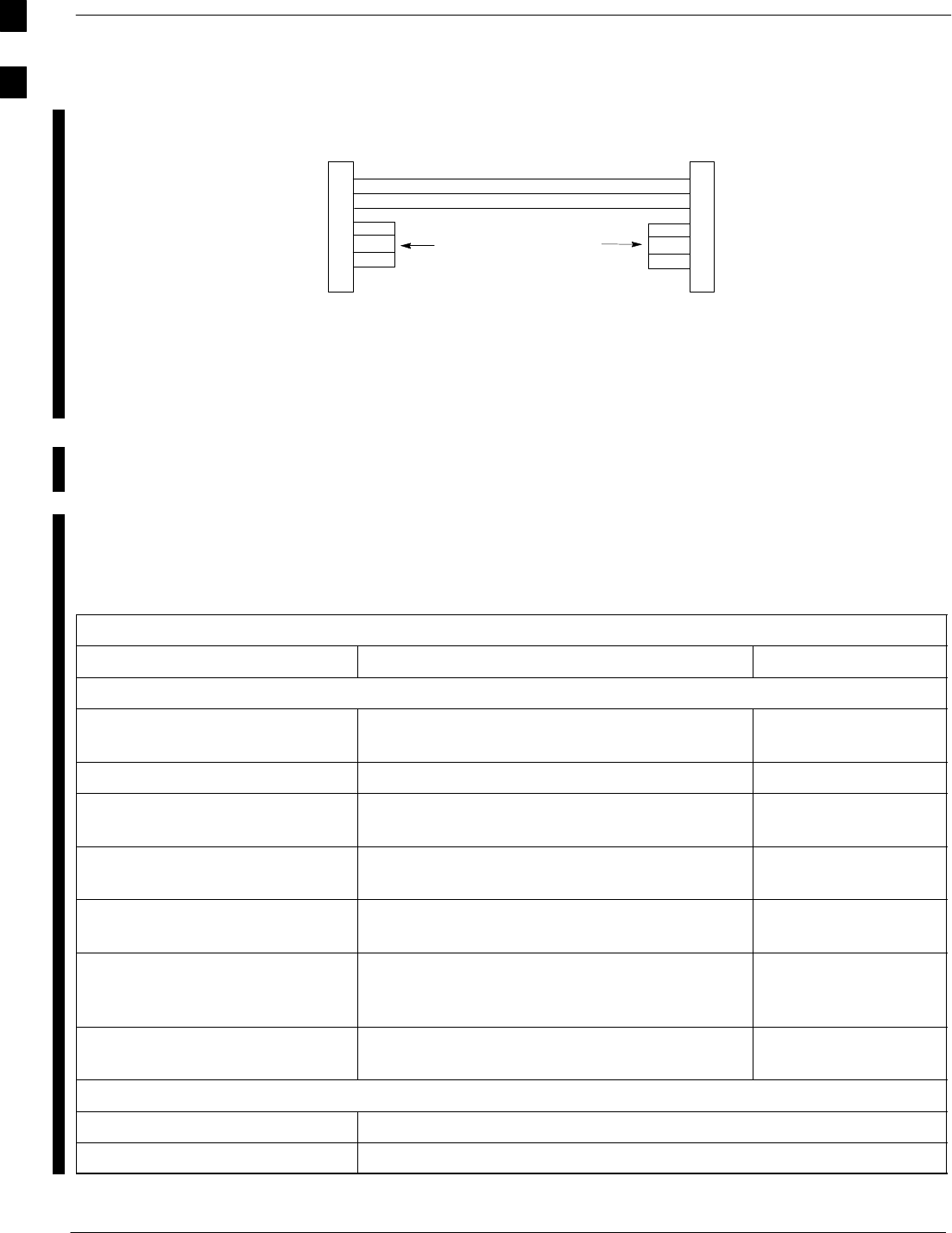
Required Test Equipment and Software – continued
1-8 1X SC 4812T Lite BTS Optimization/ATP FEB 2005
PRELIMINARY
5
3
2
7
1
4
6
GND
RX
TX
RTS
RSD/DCD
DTR
DSR
GND
TX
RX
RTS
RSD/DCD
DTR
DSR
ON BOTH
CONNECTORS:
SHORT PINS 7, 1, 4, 6
9–PIN D–FEMALE 9–PIN D–FEMALE
5
2
3
7
1
4
6
Figure 1-1: Null Modem Cable Detail
Model SLN2006A MMI Interface Kit
SMotorola Model TRN9666A Null Modem Board. Connectors on
opposite sides of the board must be used as this performs a Null
Modem Transformation between cables. This board can be used for
25–pin to 8–pin, 25–pin to 25–pin, and 10–pin to 10–pin conversions.
SMotorola 30–09786R01 MMI Cable or equivalent; used to interface
the LMF Computer Serial Port Connection to the Group Line Interface
(GLI), Clock Synchronization Manager (CSM), External Trunked
Interface Board (ETIB), and Module Debug Serial Ports.
Communications System
Analyzer CDMA/Analog
Table 1-1: CDMA LMF Test Equipment Support Table
Item Description Test Capability
Test Sets
Hewlett Packard, Model
HP 8921A (with 83203B) Communications Analyzer (includes 83203B
CDMA Interface Option) IS–95A/B only
Motorola CyberTest Communications Analyzer IS–95A/B only
Advantest R3465 (with 3561L) Communications Analyzer (with 3561 CDMA
option) IS–95A/B only
Agilent E4406A (with E4432B) Communications Analyzer (with Generator) IS–95A/B and
CDMA 2000 Testing
Advantest R3267 Analyzer (with
R3562) Communications Analyzer with Advantest
R3562 Generator IS–95A/B and
CDMA 2000 Testing
Agilent 8935 Series E6380A
(formerly HP 8935) with Option
200 or R2K
Communications Test Set IS–95A/B and
CDMA 2000 Testing
Agilent E7495A Communications Test Set IS–95A/B and
CDMA 2000 Testing
Power Meters
Gigatronix 8541C Power Meter
HP437B (with HP8481A Sensor) Power Meter with Sensor – capable of measuring –30dBm to 20dBm
1

Required Test Equipment and Software – continued
FEB 2005 1X SC 4812T Lite BTS Optimization/ATP 1-9
PRELIMINARY
A combination of Test Equipment supported by the LMF may also be
used during Optimization and Testing of the RF Communications
Portion of BTS Equipment when the Communications System Analyzer
does not perform all of the following functions:
SFrequency Counter
SDeviation Meter
SRF Power Meter (Average and Code Domain)
SRF Signal Generator (capable of DSAT/CDMA Modulation)
SAudio Signal Generator
SAC Voltmeter (with 600 Ohm Balanced Audio Input and High
Impedance Input Mode)
SNoise Measurement Meter
SC–Message Filter
SSpectrum Analyzer
SCDMA Code Domain Analyzer
GPIB Cables
Hewlett Packard 10833A or equivalent; one or two meters long, used to
interconnect Test Equipment and LMF Computer.
Timing Reference Cables
STwo Huber & Suhner 16MCX/11BNC/K02252D or equivalent; right
angle MCX–Male to standard BNC–Male RG316 Cables; 10 ft. long
are required to interconnect the Communications System Analyzer to
SGLN4132A and SGLN1145A CSM Card Timing References.
or
STwo BNC–Male to BNC–Male RG316 Cables; 3 meters (10 feet)
long, used to interconnect the Communications System Analyzer to
SGLN4132B and SGLN1145B (and later) CSM Front Panel Timing
References in the RF Modem Frame.
Digital Multimeter
Fluke Model 8062A with Y8134 Test Lead Kit or equivalent; used for
precision DC and AC Measurements to four decimal places.
Directional Coupler
Narda Model 3020A 20dB Coupler terminated with two Narda Model
375BN–M Loads, or equivalent.
RF Attenuators
S20dB Fixed Attenuator, 20 Watt (Narda 768–20), used in conjunction
with Calibration of Test Cables or during General Troubleshooting
Procedures.
S10 dB Fixed Attenuator, 20 Watt (Narda 768–10), for Cable
Calibration with a Cybertest CDMA Analyzer.
1

Required Test Equipment and Software – continued
1-10 1X SC 4812T Lite BTS Optimization/ATP FEB 2005
PRELIMINARY
Clamp–on DC Current Probe
Amprobe CT600, or equivalent, 600 Amp Capability with jaw size that
accommodates 4/0 Cable. Used with the DMM for Back–up Battery
Charging Tests.
Miscellaneous RF Adapters, Loads, etc.
As required to interface Test Cables and BTS Equipment and for various
Test Set–ups. Should include at least (2) 50 Ohm Loads (Type N) for
Calibration and (1) RF Short.
RF Load
100W Non–radiating RF Load used (as required) to provide Dummy RF
Loading during BTS Transmit Tests.
High Impedance Conductive Wrist Strap
Motorola Model 42–80385A59; used to prevent damage from ESD when
handling or working with cards/modules.
Driver Bit for Tamper–resistant Fasteners
Star fastener tamper–resistant insert bit set, Grainger 5F530 or
equivalent, to remove tamper–resistant fasteners securing the BTS Frame
Rear Access Cover.
Optional Equipment
This section provides a list of additional equipment that might be
required during Maintenance and Troubleshooting Operations.
Not all optional equipment specified in this section is
supported by the LMF in automated tests.
NOTE
Duplexer
Filtronics Low IM Duplexer (Cm035–f2) or equivalent; used during
Spectral Purity Receive Band Noise Tests.
Frequency Counter
Stanford Research Systems SR620 or equivalent; used if direct
measurement of the 3 MHz or 19.6608 MHz references is required.
Spectrum Analyzer
Spectrum Analyzer (HP8594E with CDMA Personality Card) or
equivalent; required for manual tests other than standard Receive Band
Spectral Purity Tests performed by the LMF.
1

Required Test Equipment and Software – continued
FEB 2005 1X SC 4812T Lite BTS Optimization/ATP 1-11
PRELIMINARY
LAN Tester
Model NETcat 800 LAN Troubleshooter (or equivalent); used to
supplement LAN Tests using the ohm meter.
Span Line (T1/E1) Verification Equipment
As required for the local application.
RF Test Cable (if not provided with Test Equipment)
Motorola Model TKN8231A; used to connect Test Equipment to the
BTS Transmitter Output during Optimization or during General
Troubleshooting Procedures.
Oscilloscope
Tektronics Model 2445 or equivalent; used for Waveform Viewing,
Timing, and Measurements, or during General Troubleshooting
Procedures.
2–Way Splitter
Mini–Circuits Model ZFSC–2–2500 or equivalent; used to provide the
Diversity Receive Input to the BTS.
CDMA Subscriber Mobile or Portable Radiotelephone
Safco Model 2136–150 with Power Supply Module and Antenna; used
to provide Test Transmission and Reception during BTS Maintenance
and Troubleshooting. Do not substitute other models that do not feature
special test modes. Two radios will be required for system and
drive–around testing after Optimization and BTS ATP are completed.
RF Circulator
Circulator (FERROCOM 5809866C01) or equivalent; can substitute for
a Duplexer during Receive Sensitivity Frame Erasure Rate (FER)
Testing in conjunction with Safco CDMA Mobile.
High Stability 10 MHz Rubidium Standard
Stanford Research Systems SR625 or equivalent. Required for CSM and
High Stability Oscillator (HSO) Frequency Verification.
1

Required Documents and Related Publications
1-12 1X SC 4812T Lite BTS Optimization/ATP FEB 2005
PRELIMINARY
Required Documents
The following documents are required to perform Optimization of the
Cell Site equipment:
SSite Document (generated by Motorola Systems Engineering), that
includes:
– General Site Information
– Floor Plan
– RF Power Levels
– Frequency Plan (includes Site PN and operating frequencies)
– Channel Allocation (Paging, Traffic, etc.)
– Card/Module Placement
– Site Wiring List
– CDF or NECF Files (bts–#.cdf and cbsc–#.cdf or bts–#.necf and
cbsc–#.necf)
SDemarcation Document (Scope of Work Agreement)
SEquipment Manuals for non-Motorola Test Equipment
Related Publications
Additional, detailed information about the installation, operation, and
maintenance of the 1X SCt4812T–Lite BTS and its components is
included in the following publications:
SCellular System Administration – CDMA OnLine Documentation
S1X SC4812 Series Circuit BTS Troubleshooting Manual
(68P09262A65)
S1X SC4812 Series Packet BTS Troubleshooting Manual
(68P09262A65)
S1X SC4812T Lite BTS FRU manual (68P09262A60)
S1X SC4812T Lite Hardware Installation manual (68P09262A57)
SCFC and CDL Reference (68P09262A17)
SLMF CDMA CLI Reference (68P09262A25)
SLMF On–Line Help
1

Terms and Abbreviations
FEB 2005 1X SC 4812T Lite BTS Optimization/ATP 1-13
PRELIMINARY
Standard and Non–standard
Terms and Abbreviations
Standard terms and abbreviations used in this manual are defined in
Cellular Glossary of Terms and Acronyms; 68P09213A95. Any
non–standard terms or abbreviations included in this manual are listed in
Table 1-2.
Table 1-2: Non–Standard Terms and Abbreviations
Term or
Abbreviation Definition
1X One of two bandwidths currently defined in the IS–2000 CDMA Specification, that
extends the capability of the IS–95A and B Specifications.
1X Bandwidth provides Wireless Packet Voice and Data Transmission Capability at up to
144 Kbps.
BBX–1X Broad Band Transceiver, 1X. Third Generation BBX Card with CDMA2000 1X Packet
as well as IS–95A/B Capability.
BBXR Redundant BBX for a SCCP Cage or Cage.
CCD Clock Combining and Distribution.
SCCP Cage Card that accepts Timing Signals from the active source and distributes them
to other SCCP Cage Cards/Modules.
CIO Combiner Input/Output
DBPF Dual Bandpass Filter
DBM Debug Monitor
DLM DownLoad Manager.
A Software Application resident on the GLI Card that permits download of software
upgrades from the Centralized Base Station Controller (CBSC) to BTSs without the need
for a site visit.
DMAC Digital Metering, Alarm, Control
Part of the Meter Alarm Panel (MAP) that provides control of and status information for
the AC Power Rectifiers as well as Back–up Battery monitoring and test capability.
– This term is used interchangeably with MAP. Refer to below.
DPLL Digital Phase–Locked Loop
DRF Duplexer, TX/RX Filter.
Provides duplexing of BTS transmit and Receive Signals to one antenna per sector.
– Each RF Path may contain a Dual Directional Coupler on each Antenna Port that
allows sampling of Antenna Signals in the Forward (Transmit) and Reflected
(Receive) Directions for use by an RF Diagnostic Subsystem (RFDS).
table continued on next page
1

Terms and Abbreviations – continued
1-14 1X SC 4812T Lite BTS Optimization/ATP FEB 2005
PRELIMINARY
Table 1-2: Non–Standard Terms and Abbreviations
Term or
Abbreviation Definition
EMPC Expansion Multi–coupler Preselector Card.
BTS Expansion Frame MPC Card that is used to receive, amplify, and distribute RX
Signals from the Starter Frame MPC.
GLI3 Group Line Interface Card, third generation
Supports Packet Backhaul.
HSO High Stability Oscillator.
Module providing Back–up Timing Source for a BTS when the Timing Signal from the
GPS or Remote GPS Unit is unavailable.
HSO2 HSO Card, second generation
HSOX HSO Expansion.
Card used in a BTS Expansion Frame to interface with the Starter Frame HSO and
distribute the Timing Signals to the Expansion Frame CSM Cards.
ISC In–Service Calibration.
Technique for performing Calibration sector by sector on a BTS to avoid completely
removing the site from service.
LPAC Linear Power Amplifier Controller
MAP Meter Alarm Panel.
1X SC4812T Lite BTS FRU manual (68P09262A60) that contains the functions of both
the Temperature Compensation Panel (TCP) and the DMAC.
– Term is used interchangeably with DMAC.
MCC–1X Multi–channel CDMA Card supporting 16 or 48 CDMA2000 1X or (with Software
Release 2.16.0.84.3 and higher) IS–95A/B Channels.
MPC Multi–coupler Preselector Card.
BTS SCCP Cage Card used to amplify and distribute RX Signals to BBX Cards.
NECB Network Element Configuration Baseline
NECF Network Element Configuration File
NECJ Network Element Configuration Journal
OLF Object List File.
File containing a list of the ROM and RAM Code Versions that should be operating on
every device installed in a BTS.
The file is resident on the Central Base Station Controller (CBSC) Mobility Manager
(MM) and is passed to the GLI after a DLM Job is invoked.
The GLI uses the OLF to determine which devices require Code Download to meet the
OLF–specified Version.
table continued on next page
1

Terms and Abbreviations – continued
FEB 2005 1X SC 4812T Lite BTS Optimization/ATP 1-15
PRELIMINARY
Table 1-2: Non–Standard Terms and Abbreviations
Term or
Abbreviation Definition
PDA Power Distribution Assembly.
Assembly in an SC4812T Lite BTS providing internal DC Power Distribution and
Circuit Protection.
RFMF RF Modem Frame
RGD Remote Global Positioning System (GPS) Distribution
Module that provides distribution of Digital Timing Information to up to four BTS RF
Modem Frames from a single Remote GPS Receiver.
RGPS Remote Global Positioning System
GPS Receiver and Signal Distribution Subsystem that provides Digital Timing
Information for up to four BTS RF Modem Frames at a Cell Site.
RGPS Expansion
Primary Frame BTS Frame where the RGD is located and that serves as the Distribution Point for RGPS
Digital Timing Signals to other (Secondary) BTS Frames at a Cell Site.
RGPS Expansion
Secondary Frame BTS Frame that receives RGPS Digital Timing Signals distributed from the Primary
RGPS Expansion Frame at a Cell Site.
RHSO Remote High–Stability Oscillator
Subsystem that generates and distributes Synchronization Signals from a single HSO to
up to four RF Modem Frames.
SCCP Small CDMA Channel Processor
The type of SCCP Cage used in the SC4812ET Lite BTS.
TRF Transmit and Receive Filter
TRFs contains separate Transmit and Receive Paths and Bandpass Filters that are not
connected electrically.
Transmit and Receive Antenna Signals are not duplexed and must be handled by separate
antennas.
Each RF Path may contain a Dual Directional Coupler on each Antenna Port that allows
sampling of Antenna Signals in the Forward (Transmit) and Reflected (Receive)
Directions for use by an RFDS.
1

BTS Equipment Identification
1-16 1X SC 4812T Lite BTS Optimization/ATP FEB 2005
PRELIMINARY
Equipment Overview
Stand-Alone Frame
The 1X SCt4812T–Lite BTS Frame consists of a single cabinet
containing RF and Power Amplifier components. The BTS may be
powered by:
S220V AC (rectified internally to +27V DC)
S–48V DC (power converted internally to +27V DC)
S+27V DC
Each frame can support up to two carriers in a 3–Sector Configuration.
Six–sector operation is not supported with any SC4812T Lite
configuration.
Figure 1-2 illustrates the external features of the BTS Frame, the single
major component of the Motorola SC4812T Lite.
Expansion Site
Where more than two carriers are desired at a T Lite BTS Site, the
original Starter Frame must be modified and an additional Expansion
Frame with one or two carriers must be employed to achieve up to 4
carriers. Like the BTS Starter Frame, each cabinet contains RF and
Power Amplifier components and employ the same Power Schemas as the
BTS Starter Frame.
The BTS Frame Cabinet is identical for Starter and Expansion Frames
except for the I/O Interconnect Panel. These differences are illustrated in
Figure 1-3 through Figure 1-7.
Frame Configurations
Starter and Expansion Frame configurations are described as follows:
Starter Frame configuration supports one or two carriers, each with
separate Antenna Sets. It can operate as a Stand–Alone BTS, or can be
modified in the field to the Expansion Frame configuration.
Expansion Frame configuration supports one or two carriers using 2:1
TX Combiners and a single Antenna Set for the frame. It operates with an
SC4812T Lite Starter Frame that has its own antennas and different
carriers. Expansion Frames share RX Signals to provide Diversity RX for
the opposite frame. Expansion Frames allow equipping a single SC4812T
Lite BTS Site with up to four carriers.
Logical BTS
The BTS Software implements the Logical BTS capability. Previously, all
BTS Frames co–located at a single site had to be identified in the network
with separate and distinct BTS ID Numbers. In the Logical BTS Feature,
all frames located at a single BTS Site are identified with unique Frame
ID Numbers (Frame ID Numbers 1, 101, 201, 301) under a single (site)
BTS ID Number.
1

BTS Equipment Identification – continued
FEB 2005 1X SC 4812T Lite BTS Optimization/ATP 1-17
PRELIMINARY
A Logical BTS can consist of up to four SC 4812T Frames. When the
LMF is connected to Frame 1 of a Logical BTS, you can access all
devices in all of the frames that make up the Logical BTS. A Logical BTS
requires a CDF/NECF File that includes Equipage Information for all of
the Logical BTS Frames and their devices and a CBSC File that includes
Channel Data for all of the Logical BTS Frames.
Logical BTS Numbering
The first BTS Frame of a Logical BTS has a –1 Suffix (e.g., BTS–812–1).
Other frames of the Logical BTS are numbered with Suffixes, –101, –201,
and –301 (e. g. BTS–812–201). When you log into a BTS, a FRAME
TAB is displayed for each BTS Frame. If there is only one frame for the
BTS, there is only one Tab (e.g., FRAME–282–1) for BTS–282.
If a Logical BTS has more than one frame, there is a separate FRAME
TAB for each BTS Frame (e.g. FRAME–438–1, FRAME–438–101, and
FRAME–438–201 for a BTS–438 that has three frames). If an RFDS is
included in the CDF/NECF File, an RFDS Tab (e.g., RFDS–438–1) is
displayed.
Actions (e.g., ATP Tests) can be initiated for selected devices in one or
more frames of a Logical BTS. Refer to the Select Devices Help Screen
for information on how to select devices.
SCCP Cage Card/Module Device ID Numbers
All cards/modules/boards in the frames at a single site, assigned to a
single BTS Number, are also identified with unique Device ID Numbers
dependent upon the BTS Frame ID Number in which they are located.
Refer to Table 1-3 and Table 1-4 and Figure 1-8 for specific Device ID
Numbers.
Table 1-3: SCCP Cage/Cage Card/Module Device ID Numbers (Top Shelf)
Card/Module ID Number (Left to Right)
Frame
#Power
(PS–1) Power
(PS–2) AMR–1 GLI3–1 MCC BBX BBX–R
(Optional) MPC/
EMPC–1
1 – – 1 1 1 2 1 2 3 R1 –
101 – – 101 101 101 102 101 102 103 R101 –
201 – – 201 201 201 202 201 202 203 R201 –
301 – – 301 301 301 302 301 302 303 R301 –
Table 1-4: SCCP Cage/Cage Card/Module Device ID Numbers (Bottom Shelf)
Card/Module ID Number (Left to Right)
Frame
# HSO CSM –1 CSM –2 CCD A CCD B AMR–2 GLI3–2 MCC BBX SW MPC/
EMPC–2
1 – 1 2 – – – 2 2 3 4 4 5 6 – –
101 – 101 102 – – – 102 102 103 104 104 105 106 – –
201 – 201 202 – – – 202 202 203 204 204 205 206 – –
301 – 301 302 – – – 302 302 303 304 304 305 306 – –
1
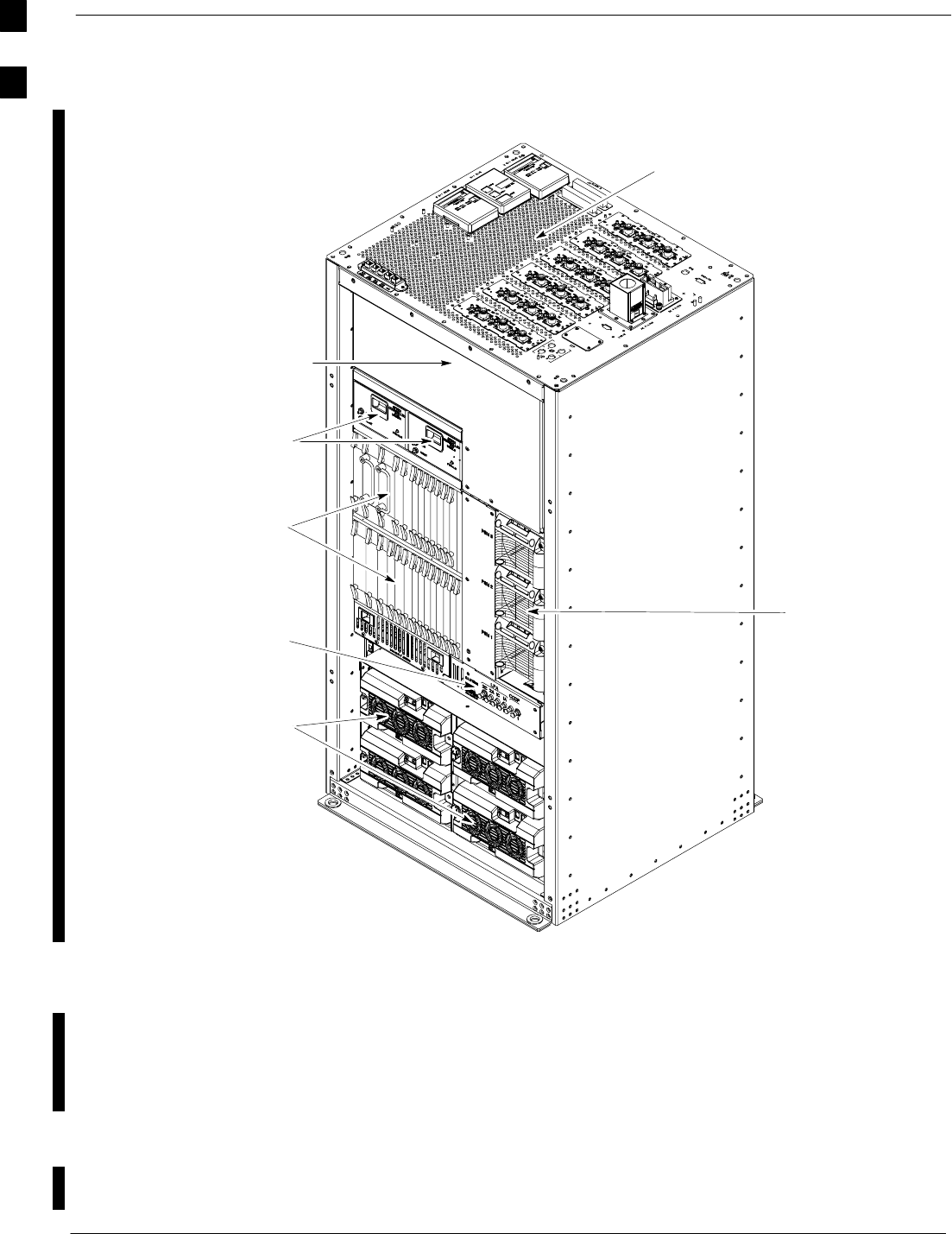
BTS Equipment Identification – continued
1-18 1X SC 4812T Lite BTS Optimization/ATP FEB 2005
PRELIMINARY
For clarity, doors are not shown.
Power
Supply
Modules
SCCP
Shelves
Fan Module
ti-CDMA-WP-00213-v01-ildoc-ftw
Power
Breaker
Panel
Amplifiers
I/O Interconnect Panel (Shown is a
2-Carrier Stand Alone Configuration; all
I/O Panel Configurations are detailed in
Figure 1-3 through Figure 1-7)
Filter
Compartment
Figure 1-2: 1X SCt4812T–Lite BTS Frame (Typical)
Internal Assemblies and FRUs
The BTS Frame houses the Fan Modules, Small CDMA Channel
Processor (SCCP) Cage, RF Power Amplifier Modules, PA Trunking
Modules.
RF Filtering includes: DRF – Duplexers with TX Filter, RX Filter, and
Diversity RX Filter and TRF – Non-Duplexed TX Filter, RX Filter, and
Diversity RX Filter.
Power System components include an AC Power Input/Filter, DC Filter,
Power Alarm Card (PAC), +27V DC Power Distribution Assembly
(PDA).
1
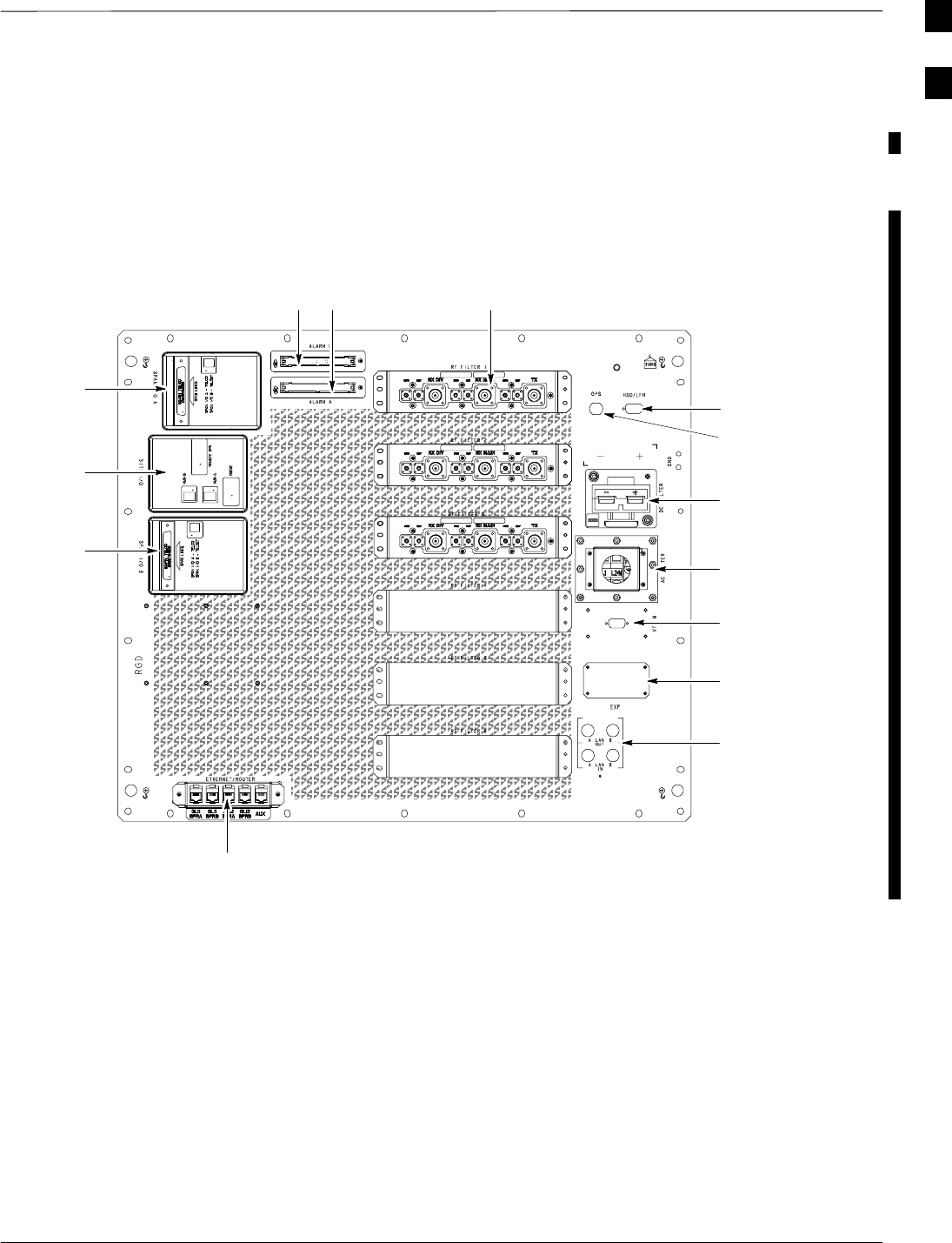
BTS Equipment Identification – continued
FEB 2005 1X SC 4812T Lite BTS Optimization/ATP 1-19
PRELIMINARY
Figure 1-2 shows the location of the internal assemblies and Field
Replaceable Units (FRUs). A brief description of each item is found in
the following paragraphs.
Figure 1-3 through Figure 1-7 show the location of components on the
I/O Interconnect Panel for the various configurations.
FRONT
SITE I/O
LAN
CONNECTIONS
GPS IN
HSO
RF FILTERING
POWER INPUT/
DC FILTER
ETHERNET ROUTER (IF USED;
OTHERWISE, FILLER PLATE)
EXP.
FILLER
PLATE
REAR
SPAN I/O
ti-CDMA-WP-00233-v01-ildoc-ftw
ALARM
CONNECTORS
POWER INPUT/
AC FILTER
SPAN I/O
VTRIM
Figure 1-3: I/O Interconnect Panel (1-Carrier Stand-Alone Frame)
1
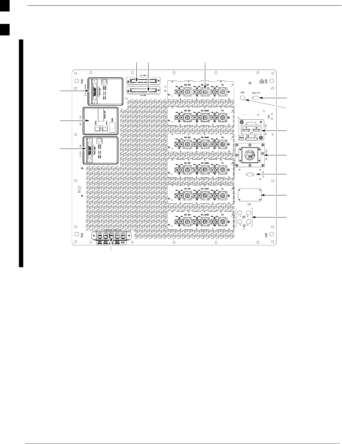
BTS Equipment Identification – continued
1-20 1X SC 4812T Lite BTS Optimization/ATP FEB 2005
PRELIMINARY
FRONT
SITE I/O
LAN
CONNECTIONS
GPS IN
HSO
RF FILTERING
POWER INPUT/
DC FILTER
ETHERNET ROUTER (IF USED;
OTHERWISE, FILLER PLATE)
EXP.
FILLER
PLATE
REAR
SPAN I/O
ti-CDMA-WP-00214-v01-ildoc-ftw
ALARM
CONNECTORS
POWER INPUT/
AC FILTER
SPAN I/O
VTRIM
Figure 1-4: I/O Interconnect Panel (2-Carrier Stand-Alone Frame)
1
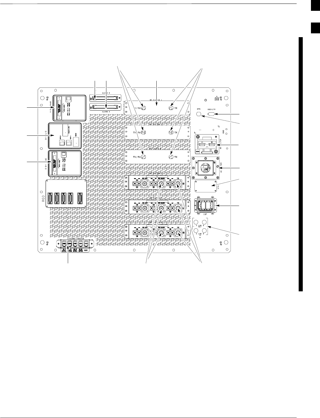
BTS Equipment Identification – continued
FEB 2005 1X SC 4812T Lite BTS Optimization/ATP 1-21
PRELIMINARY
FILTER CABLE
BULKHEAD
FRONT
SITE I/O
LAN
CONNECTIONS
GPS IN
HSO
POWER INPUT/
DC FILTER
ETHERNET ROUTER (IF USED;
OTHERWISE, FILLER PLATE)
REAR
SPAN I/O
t
i-
C
DMA-WP-
00309
-v
0
1-il
doc
-f
t
w
ALARM
CONNECTORS
POWER INPUT/
AC FILTER
SPAN I/O
VTRIM
RX1 – DIV
RX2 – DIV
RX3 – DIV
TX1 – CARRIER 2
TX2 – CARRIER 2
TX3 – CARRIER 2
RX1 – MAIN
RX2 – MAIN
RX3 – MAIN
To Combiners
(to combine
with Carrier 3)
TX1 – CARRIER 1
TX2 – CARRIER 1
TX3 – CARRIER 1
To Filters
To Antennas
RF EXPANSION PORT
TO 3RD CARRIER BTS
Figure 1-5: I/O Interconnect Panel (3-Carrier Starter Frame)
1
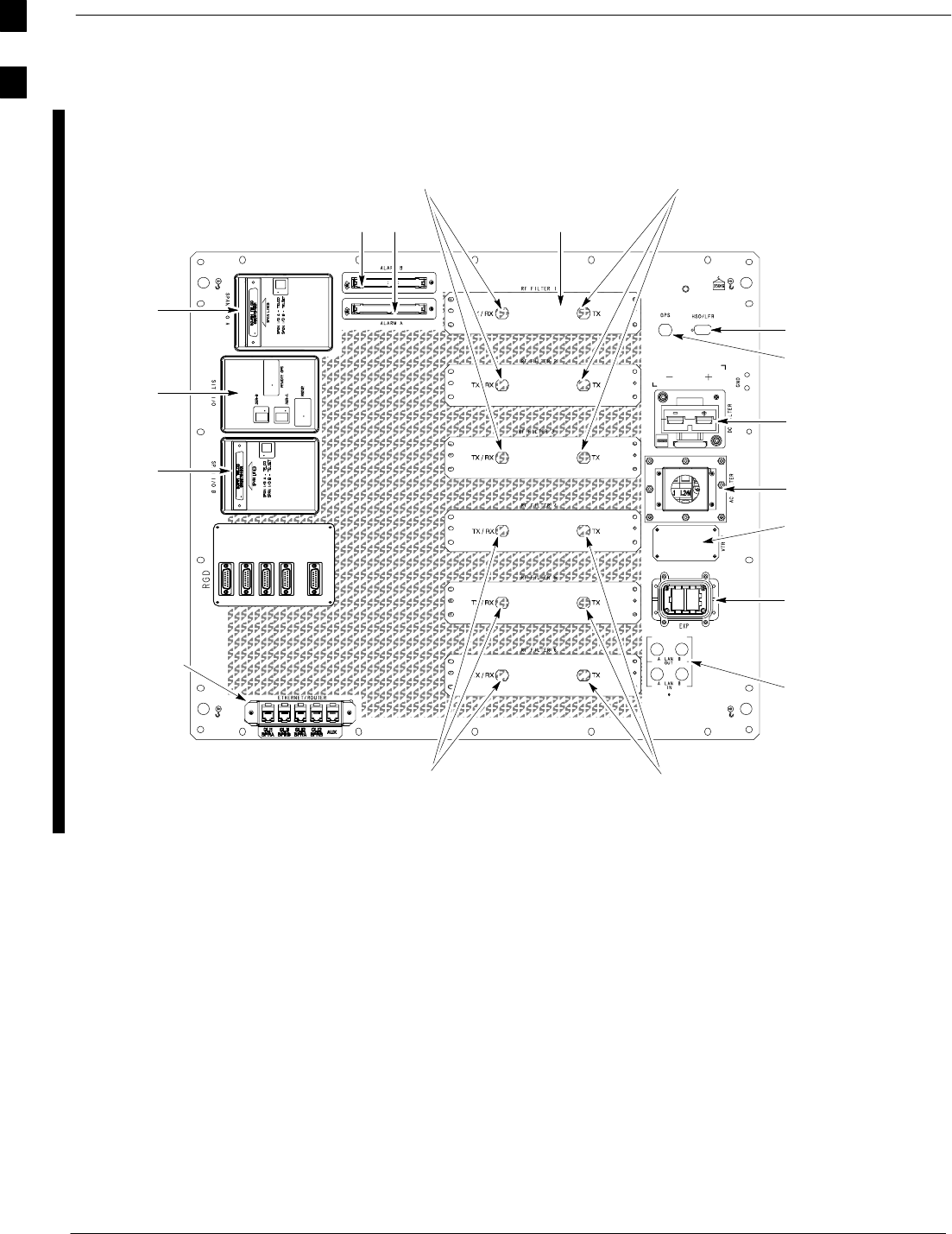
BTS Equipment Identification – continued
1-22 1X SC 4812T Lite BTS Optimization/ATP FEB 2005
PRELIMINARY
FRONT
SITE I/O
LAN
CONNECTIONS
GPS IN
HSO
POWER INPUT/
DC FILTER
REAR
SPAN I/O
ti-CDMA-WP-00310-v01-ildoc-ft
w
ALARM
CONNECTORS
POWER INPUT/
AC FILTER
SPAN I/O
VTRIM
FILTER CABLE
BULKHEAD
RX1 – DIV
RX2 – DIV
RX3 – DIV
TX1 – CARRIER 2
TX2 – CARRIER 2
TX3 – CARRIER 2
RX1 – MAIN
RX2 – MAIN
RX3 – MAIN
TX1 – CARRIER 1
TX2 – CARRIER 1
TX3 – CARRIER 1
To Combiners
(to combine
with Carrier 3)
To Filters
RF EXPANSION PORT
TO 3RD AND 4TH
CARRIER BTS
ETHERNET
ROUTER (IF
USED;
OTHERWISE,
FILLER
PLATE)
To Combiners
(to combine
with Carrier 4)
To Filters
Figure 1-6: I/O Interconnect Panel (Starter Frame – 4 Carrier)
1
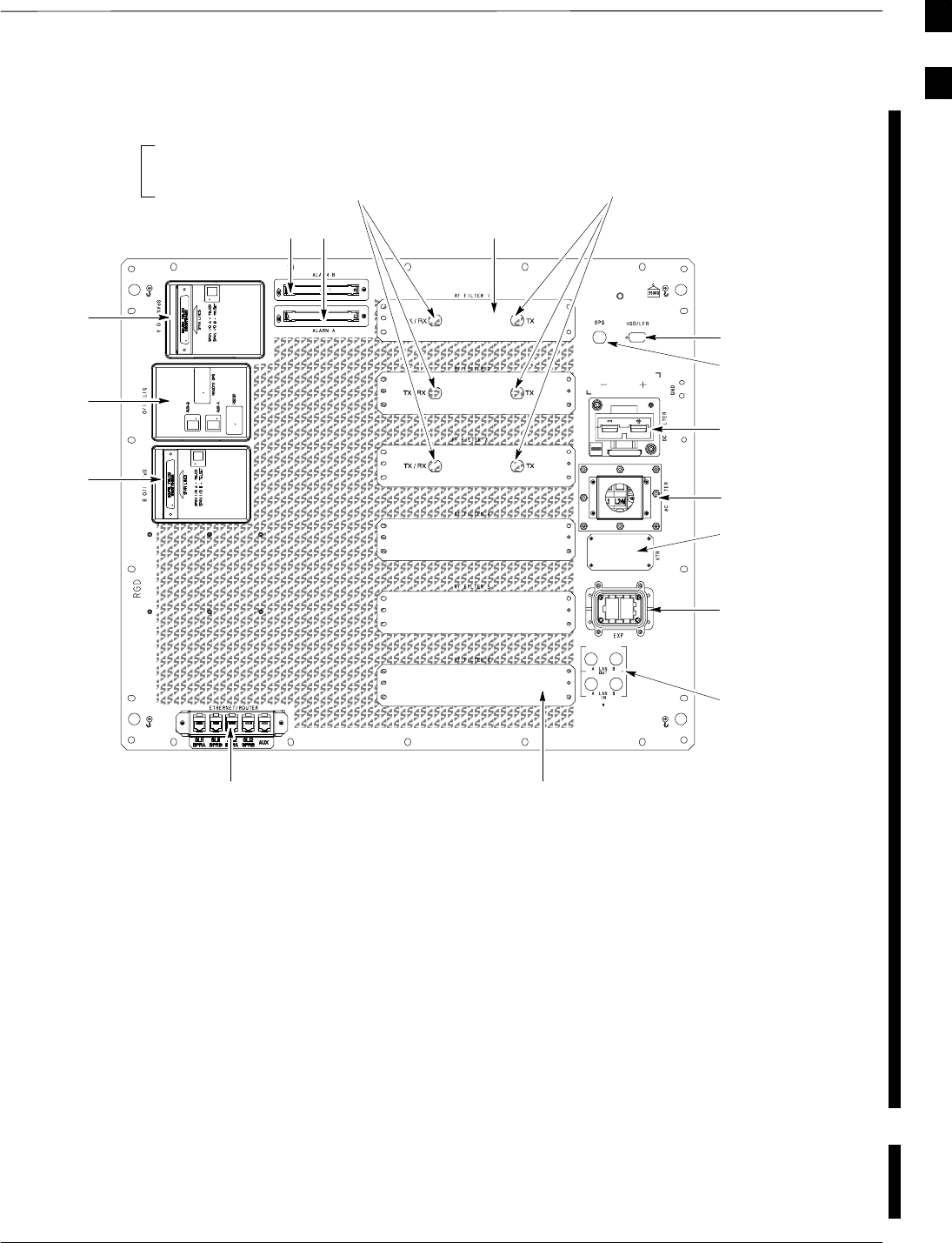
BTS Equipment Identification – continued
FEB 2005 1X SC 4812T Lite BTS Optimization/ATP 1-23
PRELIMINARY
FRONT
SITE I/O
LAN
CONNECTIONS
GPS IN
HSO
POWER INPUT/
DC FILTER
ETHERNET ROUTER (IF USED;
OTHERWISE, FILLER PLATE)
REAR
SPAN I/O
ti-CDMA-WP-00326-v01-ildoc-ftw
ALARM
CONNECTORS
POWER INPUT/
AC FILTER
SPAN I/O
VTRIM
FILTER CABLE
BULKHEAD
FILLER PLATES (3)
TX1 – CARRIER 3
TX2 – CARRIER 3
TX3 – CARRIER 3
TX1 – CARRIER 4
TX2 – CARRIER 4
TX3 – CARRIER 4
To Combiners
(to combine
with Carrier 2)
Ports are not used
on 3 Carrier
Configuration
RF EXPANSION PORT
FROM STARTER
FRAME
Figure 1-7: I/O Interconnect Panel (Expansion Frame – 3 and 4 Carrier)
DC Power Distribution Assembly (PDA)
The BTS Frame requires +27V, provided by direct input (+27V Version),
–48V to +27V Power Converters (–48V Version), or AC Rectifiers and
External Battery Back–up (AC Version). The +27V Power is then routed
to the Circuit Breaker Panel. Refer to Figure 1-2.
The Breaker Panel distributes DC Power and System DC Bus Protection
from the Loads with Distribution Circuit Breakers. The 6
post–Distribution Circuit Breakers permit removal of individual Loads.
Filter Compartment
The Filter Compartment (Figure 1-2) houses the Transmit/Receive Filters
(TRF/DRF).
Span I/O Board
The Span I/O Board (Figure 1-3) provides the Span Line Interface to the
SCCP Backplane.
1

BTS Equipment Identification – continued
1-24 1X SC 4812T Lite BTS Optimization/ATP FEB 2005
PRELIMINARY
Small CDMA Channel Processor (SCCP) Cage
The SCCP Cage has provisions for the following types and quantities of
modules (Figure 1-8):
SAlarm Monitoring and Reporting (AMR) Cards (2)
SBroad Band Transceiver, 1X, (BBX–1X) Cards, primary (6)
SBBX–1X Card, redundant (1)
SCDMA Clock Distribution (CCD) Cards (2)
SClock Synchronization Manager (CSM) on two Cards (one with GPS
Receiver, if ordered)
SCombiner Input/Output (CIO) Card (1)
SFan Modules (2)
SFiller panel (as required)
SGroup Line Interface, third generation, (GLI3) Cards (2)
SHigh Stability Oscillator (HSO) Card (Optional) (1)
SMulti–coupler Preselector Cards (MPC) (2 per Starter Frame; 1 per
Expansion Frame)
SExpansion Multi–coupler Preselector Card (EMPC) (1 per Expansion
Frame)
SMulti–Channel CDMA (MCC–1X) Cards (4)
SPower Supply Modules (2)
SSwitch Card (1)
1
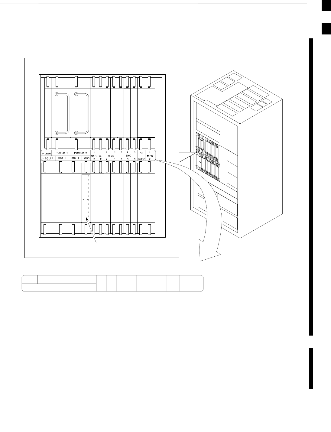
BTS Equipment Identification – continued
FEB 2005 1X SC 4812T Lite BTS Optimization/ATP 1-25
PRELIMINARY
ti-CDMA-WP-00222-v01-ildoc-ftw REF
MPC/EMPC
CSM
Power Supply
Power Supply
MPC/EMPC
CSM
CCD–1CCD–2
AMR
HSO
AMR
GLI GLI
MCC
MCC
MCC
MCC
BBX
BBX
BBX
BBX
BBX
BBX
SWITCH
19mm Filler Panel
BBX
CIO
CCD CARD(S)
(LOCATED BEHIND FILLER PANEL)
SCCP SHELF
FILLER POWER 1 POWER 2
HSO/LFR CSM 1 CSM 2 CCD AMR GLI
1 2
3 4
MCC
1 2 3
4 5 6
BBX R1
SWITCH
1
2
1
2
1
2
MPC
Figure 1-8: SCCP Cage
Transmit/Receive Filters
Duplexed TX/RX Filters (DRFs) and non–Duplexed TX/RX Filters
(TRFs) provide separate, Bandpass–Filtered Sector Transmit and Receive
Paths.
DRFs and TRFs may have Dual Directional Couplers incorporated to
permit Signal Monitoring by the RFDS. Refer to Figure 1-9.
When TRFs are used, separate Transmit and Receive Antennas are
required for each sector. DRFs permit a single Antenna Path for both the
Main RX and the TX Signal for each sector.
1
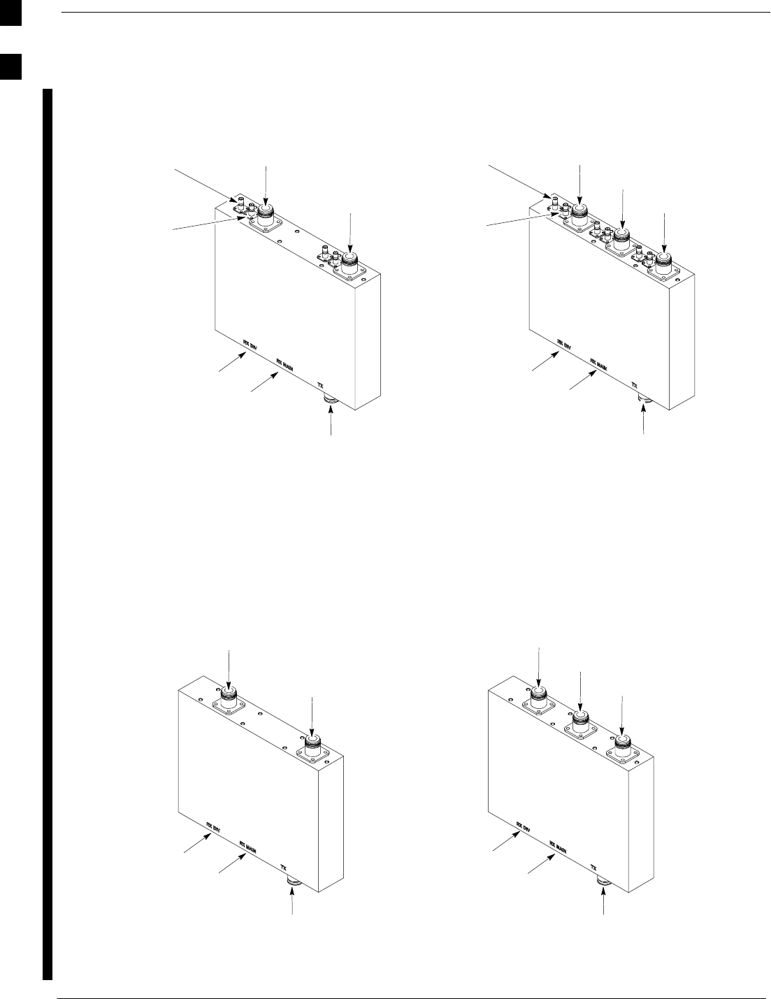
BTS Equipment Identification – continued
1-26 1X SC 4812T Lite BTS Optimization/ATP FEB 2005
PRELIMINARY
TRF
TX
ANTENNA
RX MAIN
ANTENNA
RX DIV
ANTENNA
RX DIV
TX
RX MAIN
FWD
REV
RX DIV
TX
RX MAIN
DUPLEXED
TX & RX MAIN
ANTENNA
DRF
RX DIV
ANTENNA
DIRECTIONAL
COUPLERS
(TYPICAL)
FWD
REV
DIRECTIONAL
COUPLERS
(TYPICAL)
ti-CDMA-WP-00251-v01-ildoc-ftw
Figure 1-9: DRF/TRF with Couplers Details
TRF
TX
ANTENNA
RX MAIN
ANTENNA
RX DIV
ANTENNA
RX DIV
TX
RX MAIN
RX DIV
TX
RX MAIN
DUPLEXED
TX & RX MAIN
ANTENNA
DRF
RX DIV
ANTENNA
ti-CDMA-WP-00252-v01-ildoc-ftw
Figure 1-10: DRF and TRF Details
1

BTS Equipment Identification – continued
FEB 2005 1X SC 4812T Lite BTS Optimization/ATP 1-27
PRELIMINARY
SCCP Cage Configuration and
1X Devices
SC 4812T Lite BTS Frames have one SCCP Cage that will support up to
four MCC Cards and six BBX Cards.
MCC Cards
The BTS is configured with MCC–1X Cards and with Software Release
R2.16.5.x and supports CDMA2000 1X. For additional Software Release
Compatibility and Compatibility Information, contact the local Motorola
Account Team.
BBX Cards
Up to six BBX–1X Cards can be supported. SCCP Cage Card Slots 1
through 6 are carrier–dependant and sector–dependent. The SCCP Cage
R1 Card Slot is dedicated to the Redundant BBX. Refer to Table 1-5 for
BBX Card Slot Carrier and Sector Correlations.
1

BTS Sector Configurations
1-28 1X SC 4812T Lite BTS Optimization/ATP FEB 2005
PRELIMINARY
BTS Sector Configurations
Table 1-5 and Figure 1-11 outlines the basic configurations for one- or
two-frame sites. More detailed information in Table 1-6 describes the
correlation between Sectors, BBX Cards, and Filters.
Table 1-5: SC 4812T Lite Carrier Configurations
Starter Site (1–Frame)
3–Sector/2–Adjacent Carrier Starter Frame
Carrier TX 1 TX 2 TX 3 TX 4 TX 5 TX6
1BBX–1 BBX–2 BBX–3 N/A N/A N/A
2N/A N/A N/A BBX–4 BBX–5 BBX–6
Expansion Site (2–Frames)
3–Sector/2–Non–Adjacent Carrier Starter Frame (External 2:1 Combiner)
Carrier TX 1 TX 2 TX 3 TX 4 TX 5 TX6
1BBX–1 BBX–2 BBX–3 N/A N/A N/A
3BBX–4 BBX–5 BBX–6 N/A N/A N/A
3–Sector/2–Non–Adjacent Carrier Expansion Frame (External 2:1 Combiner)
Carrier TX 1 TX 2 TX 3 TX 4 TX 5 TX6
2BBX–1 BBX–2 BBX–3 N/A N/A N/A
4BBX–4 BBX–5 BBX–6 N/A N/A N/A
Figure 1-11 shows the BTSs with fully populated CLPA
Shelves. However, the SC 4812T Lite does not currently
support 4 CLPA Modules per carrier; CLPA1D and
CLPA2D will not be present.
NOTE
1
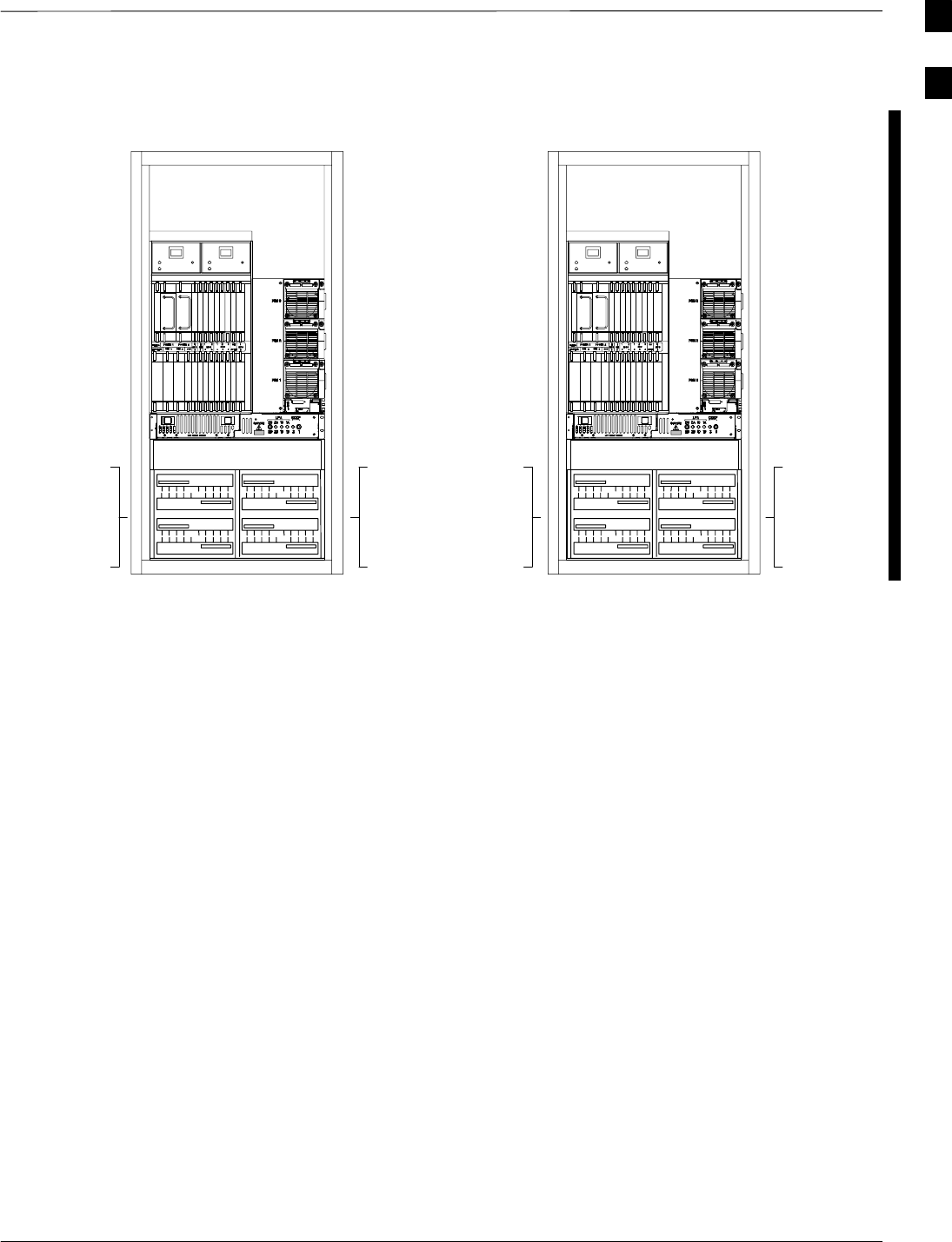
BTS Sector Configurations – continued
FEB 2005 1X SC 4812T Lite BTS Optimization/ATP 1-29
PRELIMINARY
Starter Frame
CLPA 1B
CLPA 2ACLPA 1A
CLPA 1D
CLPA 2B
CLPA 2D
CLPA 2CCLPA 1C
Expansion Frame
CLPA 1B
CLPA 2ACLPA 1A
CLPA 1D
CLPA 2B
CLPA 2D
CLPA 2CCLPA 1C
CARRIER 2
SECTOR 1, 2, 3
AT 2-FRAME
SITE
CARRIER 4
SECTOR 1, 2, 3
AT 2-FRAME
SITE
CARRIER 1
SECTOR 1, 2, 3
AT 1-FRAME
OR
2-FRAME SITE
CARRIER 2
SECTOR 1, 2, 3 AT
1-FRAME SITE
OR
CARRIER 3
SECTOR 1, 2, 3 AT
2-FRAME SITE
Figure 1-11: SC4812T Lite CLPA Configuration
1

BTS Sector Configurations – continued
1-30 1X SC 4812T Lite BTS Optimization/ATP FEB 2005
PRELIMINARY
The matrix in Table 1-6 shows the correlation between the various Sector
Configurations, Filters, Combiners, and BBX Cards.
Table 1-6: SC 4812T Lite Starter Frame Sector/Carrier Configurations
Configuration Item Sector 1 Sector 2 Sector 3 Sector 1 Sector 2 Sector 3
Filter DRF 1 DRF 2 DRF 3 N/A N/A N/A
3–Sector/ BBX BBX–1 BBX–2 BBX–3 N/A N/A N/A
3 Sector/
1–Carrier
using DRFs TX/
RX A TX Carrier 1/
RX Main
TX Carrier 1/
RX Main
TX Carrier 1/
RX Main
N/A N/A N/A
RX B RX Diversity RX Diversity RX Diversity N/A N/A N/A
Filter DRF 1 DRF 2 DRF 3 DRF 4 DRF 5 DRF6
3–Sector/ BBX BBX–1 BBX–2 BBX–3 BBX–4 BBX–5 BBX–6
3–Sector/
2–Carrier
using DRFs TX/
RX A TX Carrier 1/
RX Main
TX Carrier 1/
RX Main
TX Carrier 1/
RX Main
TX Carrier 2/
RX Main
TX Carrier 2/
RX Main
TX Carrier 2/
RX Main
RX B RX Diversity RX Diversity RX Diversity RX Diversity RX Diversity RX Diversity
Filter DRF 1 DRF 2 DRF 3 DRF 4 DRF 5 DRF6
BBX BBX–1 BBX–2 BBX–3 BBX–4 BBX–5 BBX–6
3–Sector/
3–Carrier
using DRFs
TX/
RX A TX Carriers 1
& 3 (using 2:1
Combiners)/
RX Main
TX Carriers 1
& 3 (using 2:1
Combiners)/
RX Main
TX Carriers 1
& 3 (using 2:1
Combiners)/
RX Main
TX Carrier 2/
RX Main
TX Carrier 2/
RX Main
TX Carrier 2/
RX Main
RX B RX Diversity RX Diversity RX Diversity RX Diversity RX Diversity RX Diversity
Filter DRF 1 DRF 2 DRF 3 DRF 4 DRF 5 DRF6
BBX BBX–1 BBX–2 BBX–3 BBX–4 BBX–5 BBX–6
3–Sector/
4–Carrier
using DRFs
TX/
RX A TX Carriers 1
& 3 (using 2:1
Combiners)/
RX Main
TX Carriers 1
& 3 (using 2:1
Combiners)/
RX Main
TX Carriers 1
& 3 (using 2:1
Combiners)/
RX Main
TX Carriers 2
& 4 (using 2:1
Combiners)/
RX Main
TX Carriers 2
& 4 (using 2:1
Combiners)/
RX Main
TX Carriers 2
& 4 (using 2:1
Combiners)/
RX Main
RX B RX Diversity RX Diversity RX Diversity RX Diversity RX Diversity RX Diversity
Filter TRF 1 TRF 2 TRF 3 N/A N/A N/A
3–Sector/
BBX BBX–1 BBX–2 BBX–3 N/A N/A N/A
3
–
S
ec
t
or
/
1–Carrier
i TRF
TX TX Carrier 1 TX Carrier 1 TX Carrier 1 N/A N/A N/A
using TRFs RX A RX Main RX Main RX Main N/A N/A N/A
RX B RX Diversity RX Diversity RX Diversity N/A N/A N/A
Filter TRF 1 TRF 2 TRF 3 TRF 4 TRF 5 TRF 6
3–Sector/
BBX BBX–1 BBX–2 BBX–3 BBX–4 BBX–5 BBX–6
3
–
S
ec
t
or
/
2–Carrier
i TRF
TX TX Carrier 1 TX Carrier 1 TX Carrier 1 TX Carrier 2 TX Carrier 2 TX Carrier 2
using TRFs RX A RX Main RX Main RX Main RX Main RX Main RX Main
RX B RX Diversity RX Diversity RX Diversity RX Diversity RX Diversity RX Diversity
1

FEB 2005 1X SC 4812T Lite BTS Optimization/ATP
PRELIMINARY
Chapter 2: Preparatory Tasks
Table of Contents
Preliminary Operations: Overview 2-1 . . . . . . . . . . . . . . . . . . . . . . . . . . . . . . . . . . .
Introduction 2-1 . . . . . . . . . . . . . . . . . . . . . . . . . . . . . . . . . . . . . . . . . . . . . .
Cell Site Types 2-1 . . . . . . . . . . . . . . . . . . . . . . . . . . . . . . . . . . . . . . . . . . . .
CDF/NECF 2-1 . . . . . . . . . . . . . . . . . . . . . . . . . . . . . . . . . . . . . . . . . . . . . .
Site Equipage Verification 2-1 . . . . . . . . . . . . . . . . . . . . . . . . . . . . . . . . . . .
Initial Installation of Cards/Boards/Modules 2-2 . . . . . . . . . . . . . . . . . . . .
Setting Frame SCCP Configuration Switch 2-3 . . . . . . . . . . . . . . . . . . . . .
Ethernet LAN 2-5 . . . . . . . . . . . . . . . . . . . . . . . . . . . . . . . . . . . . . . . . . . . . . . . . . . .
Ethernet LAN Termination 2-5 . . . . . . . . . . . . . . . . . . . . . . . . . . . . . . . . . .
Pre–Power–up Tests 2-6 . . . . . . . . . . . . . . . . . . . . . . . . . . . . . . . . . . . . . . . . . . . . . .
Objective 2-6 . . . . . . . . . . . . . . . . . . . . . . . . . . . . . . . . . . . . . . . . . . . . . . . .
Test Equipment 2-6 . . . . . . . . . . . . . . . . . . . . . . . . . . . . . . . . . . . . . . . . . . .
Cabling Inspection 2-6 . . . . . . . . . . . . . . . . . . . . . . . . . . . . . . . . . . . . . . . . .
DC and AC Power Pre-test (BTS Frame) 2-6 . . . . . . . . . . . . . . . . . . . . . . .
Initial Power–up Tests and Procedures 2-10 . . . . . . . . . . . . . . . . . . . . . . . . . . . . . . . .
Power-up Procedures 2-10 . . . . . . . . . . . . . . . . . . . . . . . . . . . . . . . . . . . . . . .
Common Power Supply Module Verification 2-11 . . . . . . . . . . . . . . . . . . . .
Initial Power-up (BTS) 2-12 . . . . . . . . . . . . . . . . . . . . . . . . . . . . . . . . . . . . .
Common Power Supply Module Verification 2-13 . . . . . . . . . . . . . . . . . . . .
Power Removal 2-15 . . . . . . . . . . . . . . . . . . . . . . . . . . . . . . . . . . . . . . . . . . . . . . . . . .
Introduction 2-15 . . . . . . . . . . . . . . . . . . . . . . . . . . . . . . . . . . . . . . . . . . . . . .
Remove Power 2-15 . . . . . . . . . . . . . . . . . . . . . . . . . . . . . . . . . . . . . . . . . . . .
2

Table of Contents – continued
1X SC 4812T Lite BTS Optimization/ATP FEB 2005
PRELIMINARY
Notes
2
Preliminary Operations: Overview
FEB 2005 1X SC 4812T Lite BTS Optimization/ATP 2-1
PRELIMINARY
Introduction
This section first verifies proper Frame Equipage against the
Site–specific Documentation supplied for each BTS Application. This
includes verifying Card/Module Placement, Jumper, and dual in–line
package (DIP) Backplane Configuration Switch Settings. Next,
pre-Power–up and initial power-up procedures are presented. Finally,
power–down and normal Power–up procedures are covered.
Cell Site Types
Sites are configured as Omni or up to 3–Sectors – one or two carriers.
Each type has unique characteristics and must be optimized accordingly.
CDF/NECF
The Configuration Data File (CDF) or Network Element Configuration
File (NECF) contains site type and Equipage data information and
passes it directly to the LMF during Optimization. The number of
modem frames, number and types of BBX and MCC boards, and linear
Power Amplifier assignments are some of the Equipage data included in
the CDF/NECF.
Ensure that the correct bts–#.cdf (or bts–#.necf) and
cbsc–#.CDF Files are used for the BTS.
– These should be the CDF/NECF Files that are
provided for the BTS by the CBSC.
Failure to use the correct CDF/NECF Files can cause
system errors.
Failure to use the correct CDF/NECF Files to log into
a live (traffic carrying) site can shut down the site.
IMPORTANT
*
Site Equipage Verification
Review the Site Documentation. Match the Site Engineering Equipage
Data to the actual cards, boards, and modules shipped to the site.
Physically inspect and verify that the equipment provided for the frame
is correct and undamaged.
Always wear an approved Anti–static Wrist Strap while
handling any circuit card/module to prevent damage by
Electrostatic Discharge (ESD).
After removal, the card/module should be placed on a
conductive surface or back into the anti–static packaging
in which it was shipped.
WARNING
2

Preliminary Operations: Overview – continued
2-2 1X SC 4812T Lite BTS Optimization/ATP FEB 2005
PRELIMINARY
Initial Installation of
Cards/Boards/Modules
Table 2-1: Initial Installation of Cards/Boards/Modules Procedure
nStep Action
1Refer to the Site Documentation and, if it was not previously done, slide all cards, boards, and
modules into the appropriate shelves as required.
* IMPORTANT
DO NOT SEAT the cards, boards, and modules at this time.
NOTE
On 800 MHz Systems equipped with BBXR, the Switch Card has a Configuration Switch that
must match the Site Configuration.
– Refer to Figure 2-1.
Non–redundant systems do not require a Switch Card.
2As the actual site hardware is installed, record the Serial Number of each module on a “Serial
Number Checklist” in the Site Logbook.
The Configuration Switch (shown in Figure 2-1) is a feature on the
newer versions of the 800 Mhz Switch Card (some earlier cards do not
have the Configuration Switch).
The configuration shown in Figure 2-1 is for a 3–Sector BTS.
– Switch 1 chooses BTS or MF.
– Switches 2 and 3 are not used.
– Switch 4 chooses 3–Sector or 6–Sector.
Since the SC4812T Lite can accommodate a maximum of
three sectors, Switch 4 defaults to the 3–Sector choice.
NOTE
2
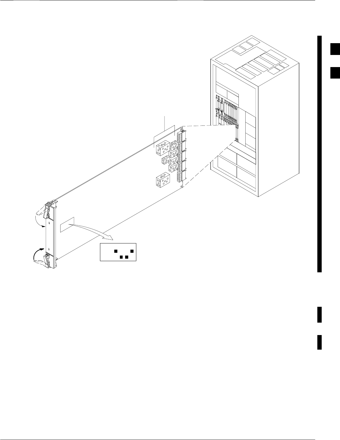
Preliminary Operations: Overview – continued
FEB 2005 1X SC 4812T Lite BTS Optimization/ATP 2-3
PRELIMINARY
ti-CDMA-WP-00228-v01-ildoc-ftw REF
Switch Card
1234
ON
BTS
MF
3–Sector
6–Sector
J1
J2
J3
J4
J5
SHIELDS
Configuration
Switch
Figure 2-1: 800 MHz Configuration Switch Card
Setting Frame SCCP
Configuration Switch
The Backplane Configuration Switch is located behind the BTS Frame
Rear Access Panel. It must be set for the BTS Frame Type as shown in
Figure 2-2.
The Backplane Configuration Switch Setting must be verified and set
before power is applied to the BTS Equipment.
2
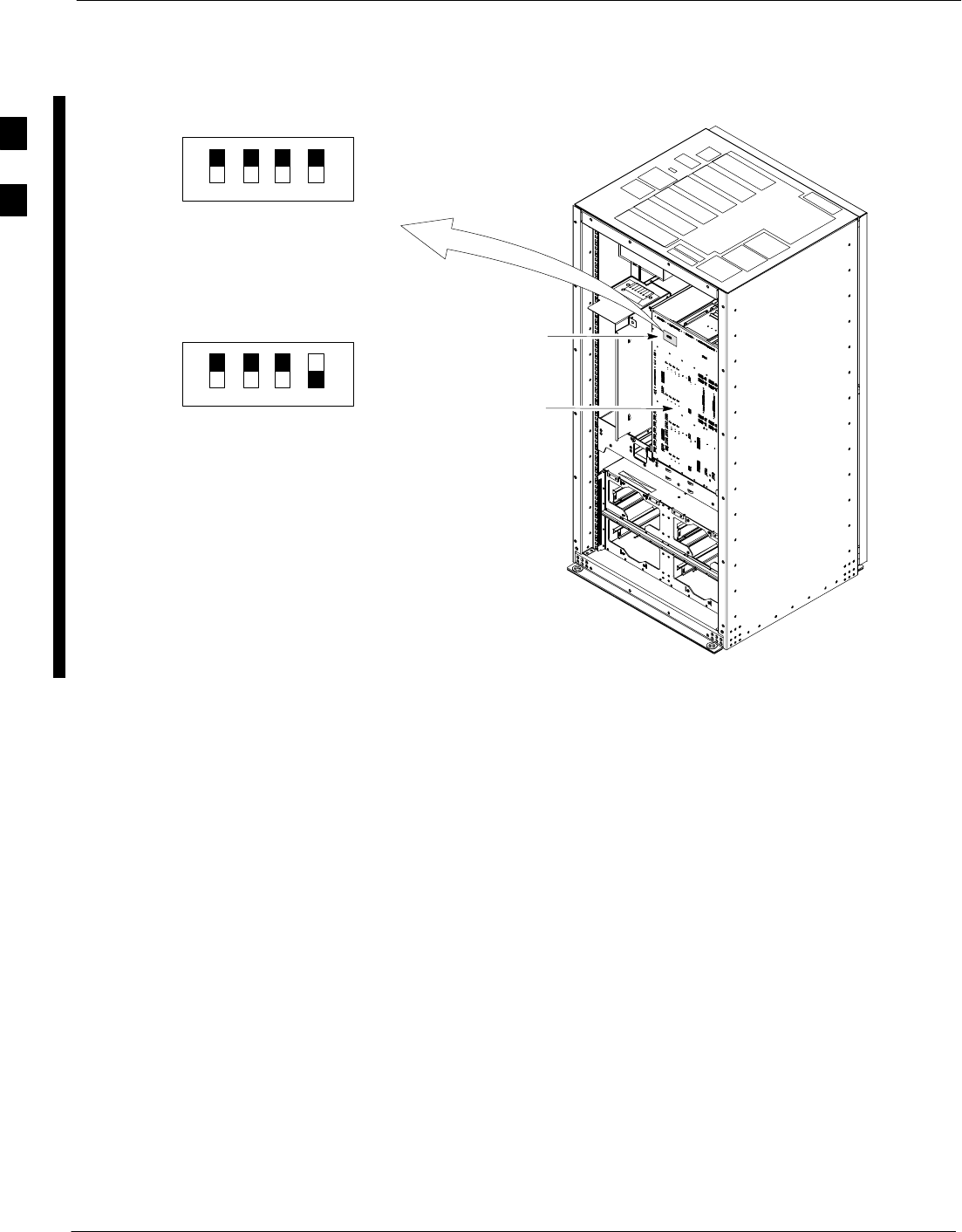
Preliminary Operations: Overview – continued
2-4 1X SC 4812T Lite BTS Optimization/ATP FEB 2005
PRELIMINARY
ON
OFF
STARTER
FRAME
SETTING
ON
OFF
EXPANSION
FRAME 1
SETTING
BOTTOM / TOP
RIGHT / LEFT
MODEM_FRAME_ID_1
MODEM_FRAME_ID_0
BOTTOM / TOP
RIGHT / LEFT
MODEM_FRAME_ID_1
MODEM_FRAME_ID_0
(REAR ACCESS
PANEL
REMOVED)
Rear of
SC 4812T Lite
SCCP
BACKPLANE
DIP SWITCH
ti-CDMA-WP-00256-v01-ildoc-ftw
Figure 2-2: Backplane DIP Switch Settings
2
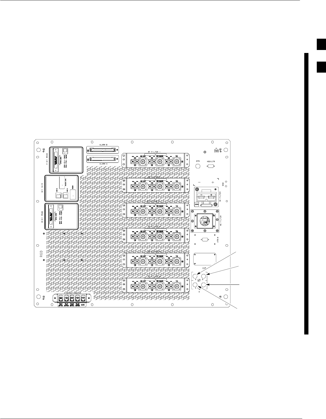
Ethernet LAN
FEB 2005 1X SC 4812T Lite BTS Optimization/ATP 2-5
PRELIMINARY
Ethernet LAN Termination
For proper operation, each end of the Primary and Redundant BTS
Ethernet Local Area Networks (LANs) must be terminated with a 50
Ohm Load. For a BTS consisting of a Stand–Alone or an Expansion
Frame, this is done by placing 50 Ohm Tri–axial Terminators on the
LAN A and B External IN and OUT Connectors.
Check the LAN A and B External IN and OUT Connectors on the I/O
Panel of each BTS Frame. Refer to Figure 2-3. Ensure terminators are
installed on all the uncabled External LAN Connectors.
FRONT
REAR
ti-CDMA-WP-00214-v01-ildoc-ftw REF
LAN B IN
CONNECTION
LAN B OUT
CONNECTION
LAN A OUT
CONNECTION
LAN A IN
CONNECTION
Figure 2-3: External Ethernet LAN Connectors
2
Pre–Power–up Tests
2-6 1X SC 4812T Lite BTS Optimization/ATP FEB 2005
PRELIMINARY
Objective
This procedure checks for any electrical short circuits and verifies the
operation and tolerances of the Cell Site and BTS Power Supply
Modules prior to applying power for the first time.
Test Equipment
The following Test Equipment is required to complete the Pre–Power–up
Tests:
SDigital Multimeter (DMM)
Always wear a Conductive, High Impedance Wrist Strap
while handling the any circuit card/module to prevent
damage by Electrostatic Discharge (ESD).
CAUTION
Cabling Inspection
Using the Site–specific Documentation generated by Motorola Systems
Engineering, verify that the following Cable Systems are properly
connected:
SReceive RF Cabling – up to 12 RX Cables
STransmit RF Cabling – up to six TX Cables
SGPS
SThe Negative DC Power Cable is colored red or blue.
SThe Positive DC Power Cable (Ground) is colored
black.
NOTE
DC and AC Power Pre-test
(BTS Frame) Before applying any power to the BTS Frame, perform the procedure in
Table 2-2 while referring to Figure 2-4 to verify that there are no shorts
in the BTS Frame DC and AC Distribution System.
Table 2-2: DC and AC Power Pre–test (BTS Frame) Procedure
nStep Action
1Physically verify that all DC and AC Power Sources supplying electric power to the BTS Frame
are OFF (Customer Breakers open, i.e.: High Impedance).
2Perform the following actions on each BTS Frame.
table continued on next page
2

Pre–Power–up Tests – continued
FEB 2005 1X SC 4812T Lite BTS Optimization/ATP 2-7
PRELIMINARY
Table 2-2: DC and AC Power Pre–test (BTS Frame) Procedure
nActionStep
2a Unseat all circuit boards (except the CCD and CIO Cards) in the SCCP Cage and CLPA Shelves,
but leave them in their associated slots.
2b Set both of the SCCP Cage Circuit Breakers to the OFF position by pulling out their Power
Distribution Circuit Breakers (labeled SCCP 1 and SCCP 2).
– These circuit breakers are located on the Power Distribution Panel.
2c Set the four CLPA Circuit Breakers to the OFF position by pulling out the CLPA Circuit
Breakers (four Circuit Breakers, labeled LPA 1A–1D through LPA 2A–2D).
– These circuit breakers are located on the Power Distribution Panel.
2d Select your type of BTS Frame.
SProceed to Step 3 for –48V Systems.
SProceed to Step 4 for +27V Systems.
3For –48V Configurations ONLY:
Perform the following actions to verify that the resistance on the –48V Bus.
3a Remove the Power Supply Modules (PSMs).
3b Verify that the resistance from the Positive (+) Power Feed Terminal with respect to the Ground
Terminal on the top of the frame measures > 500 Ω.
– Refer to Figure 2-4.
3c Verify that the resistance from the Negative (–) Power Feed Terminal with respect to the Ground
Terminal on the top of the frame measures > 500 Ω.
– This assumes that Customer Interface Cabling and Grounding has been installed; otherwise,
the measurement should be < 5 Ω.
– Refer to Figure 2-4.
4For AC Configurations ONLY:
Perform the following actions to verify that the resistance on the AC Frame.
n WARNING
Ensure that the AC Circuit Breaker is OFF (and tagged/locked) prior to proceeding.
Confirm that AC Voltage is not being applied to the BTS Frame.
4a Measure the resistance from L1 with respect to the Ground Terminal on the top of the frame
measures >10 kilohm.
– Refer to Figure 2-4.
4b Access the L1 Terminal on the AC Filter or probe the L1 Socket in the PSM Slot.
– Lightly probe the socket to avoid damaging the socket.
4c Measure the resistance from L2/N with respect to the Ground Terminal on the top of the frame
measures >10 kilohm.
– Refer to Figure 2-4.
table continued on next page
2

Pre–Power–up Tests – continued
2-8 1X SC 4812T Lite BTS Optimization/ATP FEB 2005
PRELIMINARY
Table 2-2: DC and AC Power Pre–test (BTS Frame) Procedure
nActionStep
4d Access the L2/N terminal on the AC Filter or probe the L2/N socket in the PSM Slot.
– Lightly probe the socket to avoid damaging the socket.
4e If the reading is < 500 Ω, an electrical short may be present somewhere in the AC Filter and PSM
Shelf.
– Isolate the problem and correct it before proceeding.
5Insert and lock the DC/DC Converter Modules for the SCCP Cage into their associated slots one
at a time.
! CAUTION
Verify that the correct Power Supply Modules are be ing used by checking the Locking/Retracting
Tabs. They should appear as follows.
STPN4009B
PWR C–CCP 4812 +27V
6Insert and lock all remaining cards, boards, and modules into their assigned slots in the SCCP
Cage.
7In the –48V and AC BTS Frames, insert the Power Supply Modules one at a time in their assigned
slots.
8Seat all CLPA and associated CLPA Fan Modules into their slots in the shelves one at a time.
2
Pre–Power–up Tests – continued
FEB 2005 1X SC 4812T Lite BTS Optimization/ATP 2-9
PRELIMINARY
DC POWER
FILTER INPUT
TOP OF SC 4812T LITE FRAME
ti-CDMA-WP-00231-v01-ildoc-ftw
AC POWER
FILTER INPUT
2A
2B
2C
2D
1A
1B
1C
1D 12
LPA SCCP
Circuit Breaker Panel
LAN
OUT
IN
LAN
AB
AB
EXP
VTRIM
AC FILTER DC FILTER
GND
GPS HSO/LFR
GROUND
(L1)
(L2 / N)
Figure 2-4: AC and DC Power Distribution Breakers and Power Feed Terminals
2
Initial Power–up Tests and Procedures
2-10 1X SC 4812T Lite BTS Optimization/ATP FEB 2005
PRELIMINARY
Power-up Procedures
Potentially lethal voltage and current levels are routed to
the BTS Equipment.
This test must be performed with a second person present
who will be acting in a safety role.
Remove all rings, jewelry, and wrist watches prior to
beginning this test.
WARNING
Input Power
In the tests to follow, power will first be verified at the input to each
BTS Frame. After power is verified, cards and modules within the frame
itself will be powered up and verified one at a time.
Before applying any power, verify that the correct Power Feed and
Return Cables are connected between the Power Supply Module Circuit
Breakers and the Power Connectors at the top of each BTS Frame.
Verify correct cable position referring to Figure 2-4 on Page 2-9.
Always wear a Conductive, High Impedance Wrist Strap
while handling any circuit card/module to prevent damage
by Electrostatic Discharge (ESD).
Extreme care should be taken during the removal and
installation of any card/module.
After removal, the card/module should be placed on a
conductive surface or back into the anti–static bag in
which it was shipped.
CAUTION
For Positive Power Applications (+27V):
– The Positive Power Cable is red.
– The Negative Power Cable is black.
For Negative Power Applications (–48V):
– The Negative Power Cable is red or blue.
– The Positive Power Cable (ground) is black.
NOTE
2

Initial Power–up Tests and Procedures – continued
FEB 2005 1X SC 4812T Lite BTS Optimization/ATP 2-11
PRELIMINARY
Make sure the Connector Adapters are securely attached
to each of the BTS Power Feeds and Returns.
Also, make sure the cables have been properly installed
into each connector.
NOTE
Common Power Supply Module
Verification
The procedure in Table 2-5 must be performed on any BTS Frame
connected to a common Power Supply Module at the site after the
common Power Supply Module has been installed and verified per the
OEM suggested Power Supply Module procedures.
Perform the following steps to verify that the Power Input is within
specification before powering up the individual cards/modules within the
frames themselves.
Table 2-3: Common Power Supply Module Verification Procedure
nStep Action
1Physically verify that all DC and AC Power Sources supplying the frame are OFF or
DISABLED.
2Perform the following actions in each BTS Frame:
2a Unseat all circuit boards (except the CCD and CIO Cards) in the SCCP Cage and LPA Shelves,
but leave them in their associated slots.
2b Set the circuit breakers to the OFF position by pulling out the SCCP and LPA Circuit Breakers.
– SCCP Cage Circuit Breakers are labeled SCCP–1 and SCCP–2.
– CLPA Circuit Breakers are labeled LPA 1A–1D through LPA 2A – 2D.
– Refer to Figure 2-4 for the Circuit Breaker Panel layout if required.
1Remove the Power Supply Modules.
2Inspect the Input Cables to verify that the correct Input Power Polarity according to the decal on
top of the frame.
3Apply power to BTS Frames, one at a time, by setting the appropriate circuit breaker in the Power
Supply Module that supplies the frame to the ON position.
4After power is applied to each BTS Frame, use a digital voltmeter to verify Power Supply Module
Output Voltages at the top of each BTS Frame are within specifications:
––48V BTS: –48V DC nominal
–+27 V BTS: +27V DC nominal
–AC BTS: 208V AC to 240V AC nominal
5Plug in the Power Supply Modules (PSMs) one at a time and verify that the PSM LEDs appear
GREEN.
2

Initial Power–up Tests and Procedures – continued
2-12 1X SC 4812T Lite BTS Optimization/ATP FEB 2005
PRELIMINARY
Initial Power-up (BTS)
The procedure in Table 2-4 must be performed on each BTS Frame after
Input Power from the common Power Supply Module has been verified.
Perform the procedure in Table 2-4 to apply initial power to the
cards/modules within the frame itself, verifying that each is operating
within specification.
Table 2-4: Initial Power–up (BTS) Procedure
nStep Action
1At the BTS, set the SCCP Power Distribution Circuit Breakers to the ON position by pushing in
the circuit breakers.
– Refer to Figure 2-4 on Page 2-9.
2Insert the SCCP Fan Modules.
– Verify that the Fan Modules come on line.
! CAUTION
Verify that the correct SCCP Power Supply Modules are being used by checking the markings on
the Locking/Retracting Tabs. Make sure that the markings appear as follows:
STPN 4009B
PWR C–CCP 4812 +27V
3Insert and lock the Power Supply Modules into their associated slots one at a time.
– If no cards are installed in the SCCP Cage, the PWR/ALM LEDs on all three Power Supply
Modules appear RED to notify the user that there is no Load on the Power Supply Modules.
– If the LED is RED, do not be alarmed. After Step 3 is performed, the LEDs should turn
GREEN; if not, then a faulty Power Supply Module is indicated and should be replaced
before proceeding.
3Seat and lock all remaining cards and modules in the SCCP Cage into their associated slots.
4Seat the first equipped LPA Module Pair into the assigned slot in the upper LPA Shelf, including
the LPA Fan.
5Repeat Step 4 for all remaining LPA Module Pairs.
! CAUTION
On frames that have CLPA Modules, engage the circuit breakers in pairs as marked on the Circuit
Breaker Panel.
NOTE
Engage the circuit breakers only for the LPA Modules that are equipped.
6Set the LPA Circuit Breakers to the ON position (per configuration) by pushing them IN.
– Confirm that the LEDs on LPA Modules light GREEN.
– Refer to Figure 2-4 for the Circuit Breaker Panel Layout.
2

Initial Power–up Tests and Procedures – continued
FEB 2005 1X SC 4812T Lite BTS Optimization/ATP 2-13
PRELIMINARY
Table 2-4: Initial Power–up (BTS) Procedure
nActionStep
7After all cards/modules have been seated and verified, use a digital voltmeter to verify that Power
Supply Module Output Voltages measured at the top of the frame remain within specifications:
–On –48V BTS: –48V DC nominal
–On +27 V BTS: +27V DC nominal
–On AC BTS: 208 to 240V AC nominal
8Repeat Steps 1 through 7 for additional co–located frames (if equipped).
Common Power Supply Module
Verification
The procedure in Table 2-5 must be performed on any BTS Frame
connected to a common Power Supply Module at the site after the
common Power Supply Module has been installed and verified per the
OEM Power Supply Module suggested procedures.
Perform the procedure in Table 2-5 to verify that the Power Input is
within specification before Power–up is attempted on the individual
cards/modules with the frames themselves.
Table 2-5: Common Power Supply Module Verification Procedure
nStep Action
1Physically verify that all DC and AC Power Sources supplying the frame are OFF or
DISABLED.
2Perform the following actions on each BTS Frame:
2a Unseat all circuit boards (except CCD and CIO Cards) in the SCCP Cage and LPA Shelves, but
leave them in their assigned slots.
2b Set the SCCP and LPA Circuit Breakers to the OFF position by pulling them out.
– SCCP Cage Circuit Breakers are labeled SCCP–1 and SCCP–2.
– CLPA Circuit Breakers are labeled LPA 1A–1D through LPA 2A–2D.
– Refer to Figure 2-4 for the Circuit Breaker Panel Layout, if required.
3Remove the Power Supply Modules.
4Inspect the Input Cables to verify that the Input Power Polarity is correct according to the decal on
top of the frame.
5Apply power to the BTS Frames one at a time.
6After power is applied to each BTS Frame, use a digital voltmeter to verify that Power Supply
Module Output Voltages at the top of each BTS Frame are within specifications:
–On –48V BTS: –48V DC nominal
–On +27 V BTS: +27V DC nominal
–On AC BTS: 208 to 240V AC nominal
table continued on next page
2

Initial Power–up Tests and Procedures – continued
2-14 1X SC 4812T Lite BTS Optimization/ATP FEB 2005
PRELIMINARY
Table 2-5: Common Power Supply Module Verification Procedure
nActionStep
7Plug in the Power Supply Modules one at a time.
8Verify that the PSM LED on each Power Supply Module appears GREEN.
2

Power Removal
FEB 2005 1X SC 4812T Lite BTS Optimization/ATP 2-15
PRELIMINARY
Introduction
DC and AC Power removal from an SC4812T Lite BTS is accomplished
by performing the procedure in Table 2-6.
Some maintenance, upgrade, or other activities may only require
removing DC Power. In those situations where all power must be
removed from a frame, removing AC Power will also be required.
Remove Power
If it becomes necessary to remove power from the frame, refer to
Figure 2-4 and perform the procedure in Table 2-6.
Table 2-6: Power Removal Procedure
nStep Action
1Set all PDA Circuit Breakers to the OFF (pulled out) position in the following sequence:
1a Pull out the four LPA Circuit Breakers labeled 1A–1D through 2A–2D.
1b Pull out the two Power Distribution Assembly (PDA) Circuit Breakers labeled SCCP–1 and
SCCP–2.
2Confirm that all LEDs are OFF except for the Power Supply Module LEDs, if present.
3Remove all DC Power Sources (+27V, –48V, or Battery Back–up) to the BTS Frame by
disengaging the appropriate Customer Circuit Breakers.
4Remove the AC Power, then lock and tag the AC Power Box (AC Frame only).
5Verify that all PSM LEDs are OFF.
n WARNING
The Surge Capacitors in the DC PDA stores large electrical charges for long periods of time.
Failure to discharge these capacitors as specified in Step 6 could result in serious personal injury
and/or damage to the equipment.
6On the DC PDA, set the SCCP1 and SCCP2 Circuit Breakers to the ON (pushed in) position, and
wait at least 30 seconds.
7Set the PDA SCCP1 and SCCP2 Circuit Breakers to the OFF position.
2

Power Removal – continued
2-16 1X SC 4812T Lite BTS Optimization/ATP FEB 2005
PRELIMINARY
Notes
2

FEB 2005 1X SC 4812T Lite BTS Optimization/ATP
PRELIMINARY
Chapter 3: Optimization/Calibration
Table of Contents
Introduction to Optimization and Calibration 3-1 . . . . . . . . . . . . . . . . . . . . . . . . . .
Overview 3-1 . . . . . . . . . . . . . . . . . . . . . . . . . . . . . . . . . . . . . . . . . . . . . . . .
Optimization Process Summary 3-1 . . . . . . . . . . . . . . . . . . . . . . . . . . . . . .
Cell Site Types 3-3 . . . . . . . . . . . . . . . . . . . . . . . . . . . . . . . . . . . . . . . . . . . .
CDF/NECF 3-4 . . . . . . . . . . . . . . . . . . . . . . . . . . . . . . . . . . . . . . . . . . . . . .
BTS System Software Download 3-4 . . . . . . . . . . . . . . . . . . . . . . . . . . . . .
Site Equipage Verification 3-5 . . . . . . . . . . . . . . . . . . . . . . . . . . . . . . . . . . .
Preparing the LMF 3-6 . . . . . . . . . . . . . . . . . . . . . . . . . . . . . . . . . . . . . . . . . . . . . . .
Overview of Packet BTS Files 3-6 . . . . . . . . . . . . . . . . . . . . . . . . . . . . . . .
LMF Features and Installation Requirements 3-7 . . . . . . . . . . . . . . . . . . . .
LMF File Structure Overview 3-8 . . . . . . . . . . . . . . . . . . . . . . . . . . . . . . . .
LMF Home Directory 3-9 . . . . . . . . . . . . . . . . . . . . . . . . . . . . . . . . . . . . . .
NECF Filename Conventions and Directory Location 3-9 . . . . . . . . . . . . .
LMF Installation and Update Procedures 3-10 . . . . . . . . . . . . . . . . . . . . . . .
Copy BTS and CBSC CDF (or NECF) Files to the LMF Computer 3-11 . .
Creating a Named HyperTerminal Connection for MMI
Communication 3-13 . . . . . . . . . . . . . . . . . . . . . . . . . . . . . . . . . . . . . . . . . .
Span Lines – Interface and Isolation 3-16 . . . . . . . . . . . . . . . . . . . . . . . . . . . . . . . . . .
T1/E1 Span Interface 3-16 . . . . . . . . . . . . . . . . . . . . . . . . . . . . . . . . . . . . . . .
Isolate the BTS from the T1/E1 Span(s) 3-16 . . . . . . . . . . . . . . . . . . . . . . . .
T1/E1 Span Isolation 3-17 . . . . . . . . . . . . . . . . . . . . . . . . . . . . . . . . . . . . . . .
LMF to BTS Connection 3-18 . . . . . . . . . . . . . . . . . . . . . . . . . . . . . . . . . . . . . . . . . .
Connect the LMF to the BTS 3-18 . . . . . . . . . . . . . . . . . . . . . . . . . . . . . . . .
Connect the LMF to the BTS at the I/O Panel 3-19 . . . . . . . . . . . . . . . . . . .
Switching the Active LAN – LMF I/O Panel 10Base–2 LAN Connection 3-21 . . . .
Switching the Active LAN 3-21 . . . . . . . . . . . . . . . . . . . . . . . . . . . . . . . . . .
Using the LMF 3-22 . . . . . . . . . . . . . . . . . . . . . . . . . . . . . . . . . . . . . . . . . . . . . . . . . .
Basic LMF Operation 3-22 . . . . . . . . . . . . . . . . . . . . . . . . . . . . . . . . . . . . . .
The LMF Display and the BTS 3-22 . . . . . . . . . . . . . . . . . . . . . . . . . . . . . . .
Graphical User Interface Operation 3-23 . . . . . . . . . . . . . . . . . . . . . . . . . . . .
Understanding GUI Operation 3-24 . . . . . . . . . . . . . . . . . . . . . . . . . . . . . . . .
Command Line Interface Overview 3-28 . . . . . . . . . . . . . . . . . . . . . . . . . . . .
Logging Into a BTS 3-28 . . . . . . . . . . . . . . . . . . . . . . . . . . . . . . . . . . . . . . . .
Logging Out 3-33 . . . . . . . . . . . . . . . . . . . . . . . . . . . . . . . . . . . . . . . . . . . . . .
Establishing an MMI Communication Session 3-34 . . . . . . . . . . . . . . . . . . .
Online Help 3-35 . . . . . . . . . . . . . . . . . . . . . . . . . . . . . . . . . . . . . . . . . . . . . .
3

Table of Contents – continued
1X SC 4812T Lite BTS Optimization/ATP FEB 2005
PRELIMINARY
Pinging the Processors 3-36 . . . . . . . . . . . . . . . . . . . . . . . . . . . . . . . . . . . . . . . . . . . .
Pinging the BTS 3-36 . . . . . . . . . . . . . . . . . . . . . . . . . . . . . . . . . . . . . . . . . .
Download the BTS 3-39 . . . . . . . . . . . . . . . . . . . . . . . . . . . . . . . . . . . . . . . . . . . . . . .
Overview 3-39 . . . . . . . . . . . . . . . . . . . . . . . . . . . . . . . . . . . . . . . . . . . . . . . .
ROM Code 3-39 . . . . . . . . . . . . . . . . . . . . . . . . . . . . . . . . . . . . . . . . . . . . . . .
RAM Code 3-39 . . . . . . . . . . . . . . . . . . . . . . . . . . . . . . . . . . . . . . . . . . . . . . .
Verify GLI ROM Code Loads 3-41 . . . . . . . . . . . . . . . . . . . . . . . . . . . . . . . .
Download RAM Code and Data to MGLI and GLI 3-42 . . . . . . . . . . . . . . .
Download RAM Code and Data to Non–GLI Devices 3-43 . . . . . . . . . . . . .
Selecting CSM Clock Source and Enabling CSM Cards 3-44 . . . . . . . . . . .
Enable MCC Cards 3-46 . . . . . . . . . . . . . . . . . . . . . . . . . . . . . . . . . . . . . . . .
CSM System Time – GPS and HSO Verification 3-47 . . . . . . . . . . . . . . . . . . . . . . . .
Clock Synchronization Manager (CSM) Subsystem Description 3-47 . . . . .
Front Panel LEDs 3-48 . . . . . . . . . . . . . . . . . . . . . . . . . . . . . . . . . . . . . . . . .
High Stability Oscillator (HSO) 3-50 . . . . . . . . . . . . . . . . . . . . . . . . . . . . . .
CSM Frequency Verification 3-50 . . . . . . . . . . . . . . . . . . . . . . . . . . . . . . . . .
Test Equipment Set–up (GPS and HSO Verification) 3-51 . . . . . . . . . . . . . .
GPS Initialization/Verification 3-53 . . . . . . . . . . . . . . . . . . . . . . . . . . . . . . . .
Connecting Test Equipment to the BTS 3-58 . . . . . . . . . . . . . . . . . . . . . . . .
Test Equipment GPIB Address Settings 3-58 . . . . . . . . . . . . . . . . . . . . . . . .
Supported Test Equipment 3-58 . . . . . . . . . . . . . . . . . . . . . . . . . . . . . . . . . . .
Test Equipment Preparation 3-59 . . . . . . . . . . . . . . . . . . . . . . . . . . . . . . . . . .
Test Equipment Connection Charts 3-59 . . . . . . . . . . . . . . . . . . . . . . . . . . . .
Equipment Warm-up 3-62 . . . . . . . . . . . . . . . . . . . . . . . . . . . . . . . . . . . . . . .
Automatic Cable Calibration Set–up 3-62 . . . . . . . . . . . . . . . . . . . . . . . . . . .
Manual Cable Calibration 3-62 . . . . . . . . . . . . . . . . . . . . . . . . . . . . . . . . . . .
Set-up for TX Calibration 3-67 . . . . . . . . . . . . . . . . . . . . . . . . . . . . . . . . . . .
Set–up for ATP 3-71 . . . . . . . . . . . . . . . . . . . . . . . . . . . . . . . . . . . . . . . . . . .
Test Equipment Set-up 3-78 . . . . . . . . . . . . . . . . . . . . . . . . . . . . . . . . . . . . . . . . . . . .
Connecting Test Equipment to the BTS 3-78 . . . . . . . . . . . . . . . . . . . . . . . .
Test Equipment GPIB Address Settings 3-78 . . . . . . . . . . . . . . . . . . . . . . . .
Supported Test Equipment 3-78 . . . . . . . . . . . . . . . . . . . . . . . . . . . . . . . . . . .
Test Equipment Preparation 3-79 . . . . . . . . . . . . . . . . . . . . . . . . . . . . . . . . . .
Test Equipment Connection Charts 3-79 . . . . . . . . . . . . . . . . . . . . . . . . . . . .
Equipment Warm-up 3-82 . . . . . . . . . . . . . . . . . . . . . . . . . . . . . . . . . . . . . . .
Automatic Cable Calibration Set–up 3-82 . . . . . . . . . . . . . . . . . . . . . . . . . . .
Manual Cable Calibration 3-82 . . . . . . . . . . . . . . . . . . . . . . . . . . . . . . . . . . .
Set-up for TX Calibration 3-87 . . . . . . . . . . . . . . . . . . . . . . . . . . . . . . . . . . .
Set–up for ATP 3-91 . . . . . . . . . . . . . . . . . . . . . . . . . . . . . . . . . . . . . . . . . . .
Test Set Calibration 3-98 . . . . . . . . . . . . . . . . . . . . . . . . . . . . . . . . . . . . . . . . . . . . . . .
Test Equipment Calibration Background 3-98 . . . . . . . . . . . . . . . . . . . . . . . .
Automatic Calibration Procedure 3-98 . . . . . . . . . . . . . . . . . . . . . . . . . . . . .
Manual Calibration Procedures 3-99 . . . . . . . . . . . . . . . . . . . . . . . . . . . . . . .
GPIB Addresses 3-99 . . . . . . . . . . . . . . . . . . . . . . . . . . . . . . . . . . . . . . . . . . .
IP Addresses 3-99 . . . . . . . . . . . . . . . . . . . . . . . . . . . . . . . . . . . . . . . . . . . . .
Selecting Test Equipment 3-99 . . . . . . . . . . . . . . . . . . . . . . . . . . . . . . . . . . .
3

Table of Contents – continued
FEB 2005 1X SC 4812T Lite BTS Optimization/ATP
PRELIMINARY
Manually Selecting Test Equipment in a Serial Connection Tab 3-100 . . . . .
Automatically Selecting Test Equipment in the Serial Connection Tab 3-102
Detecting Test Equipment when using Agilent E7495A 3-103 . . . . . . . . . . . .
Calibrating Test Equipment 3-103 . . . . . . . . . . . . . . . . . . . . . . . . . . . . . . . . . .
LMF Cables Calibration Overview 3-104 . . . . . . . . . . . . . . . . . . . . . . . . . . . .
Calibrating Test Cabling using a Communications System Analyzer 3-105 . .
Calibrate Test Cabling using a Signal Generator and Spectrum
Analyzer 3-107 . . . . . . . . . . . . . . . . . . . . . . . . . . . . . . . . . . . . . . . . . . . . . . . .
Setting Cable Loss Values 3-110 . . . . . . . . . . . . . . . . . . . . . . . . . . . . . . . . . . .
Setting TX Coupler Loss Value 3-111 . . . . . . . . . . . . . . . . . . . . . . . . . . . . . . .
Bay Level Offset Calibration 3-112 . . . . . . . . . . . . . . . . . . . . . . . . . . . . . . . . . . . . . . .
Introduction 3-112 . . . . . . . . . . . . . . . . . . . . . . . . . . . . . . . . . . . . . . . . . . . . . .
What is BLO Calibration? 3-112 . . . . . . . . . . . . . . . . . . . . . . . . . . . . . . . . . . .
BTS RF Path Descriptions 3-112 . . . . . . . . . . . . . . . . . . . . . . . . . . . . . . . . . . .
Component Verification During Calibration 3-113 . . . . . . . . . . . . . . . . . . . . .
When to Calibrate BLOs 3-113 . . . . . . . . . . . . . . . . . . . . . . . . . . . . . . . . . . . .
BLO Calibration Data File 3-114 . . . . . . . . . . . . . . . . . . . . . . . . . . . . . . . . . .
Test Equipment Set–up for RF Path Calibration 3-117 . . . . . . . . . . . . . . . . .
Transmit (TX) Path Calibration Description 3-118 . . . . . . . . . . . . . . . . . . . . .
TX Calibration and the LMF 3-119 . . . . . . . . . . . . . . . . . . . . . . . . . . . . . . . . .
TX Calibration 3-121 . . . . . . . . . . . . . . . . . . . . . . . . . . . . . . . . . . . . . . . . . . . .
All Cal/Audit and TX Calibration Procedure 3-122 . . . . . . . . . . . . . . . . . . . .
Download BLO Procedure 3-124 . . . . . . . . . . . . . . . . . . . . . . . . . . . . . . . . . . .
Calibration Audit Introduction 3-125 . . . . . . . . . . . . . . . . . . . . . . . . . . . . . . .
TX Path Audit 3-125 . . . . . . . . . . . . . . . . . . . . . . . . . . . . . . . . . . . . . . . . . . . .
TX Audit Test 3-126 . . . . . . . . . . . . . . . . . . . . . . . . . . . . . . . . . . . . . . . . . . . .
Create CAL File 3-127 . . . . . . . . . . . . . . . . . . . . . . . . . . . . . . . . . . . . . . . . . . .
RFDS Set–up and Calibration 3-129 . . . . . . . . . . . . . . . . . . . . . . . . . . . . . . . . . . . . . .
RFDS Description 3-129 . . . . . . . . . . . . . . . . . . . . . . . . . . . . . . . . . . . . . . . . .
RFDS Parameters 3-129 . . . . . . . . . . . . . . . . . . . . . . . . . . . . . . . . . . . . . . . . . .
Checking and Setting RFDS Parameters 3-130 . . . . . . . . . . . . . . . . . . . . . . . .
RFDS TSU NAM Programming 3-133 . . . . . . . . . . . . . . . . . . . . . . . . . . . . . .
Explanation of Parameters Used When Programming the TSU NAM 3-133 .
Valid NAM Ranges 3-134 . . . . . . . . . . . . . . . . . . . . . . . . . . . . . . . . . . . . . . . .
Set Antenna Map Data 3-135 . . . . . . . . . . . . . . . . . . . . . . . . . . . . . . . . . . . . . .
Set RFDS Configuration Data 3-136 . . . . . . . . . . . . . . . . . . . . . . . . . . . . . . . .
RFDS Calibration 3-137 . . . . . . . . . . . . . . . . . . . . . . . . . . . . . . . . . . . . . . . . .
TSU Program TSU NAM 3-139 . . . . . . . . . . . . . . . . . . . . . . . . . . . . . . . . . . .
Alarms Testing 3-140 . . . . . . . . . . . . . . . . . . . . . . . . . . . . . . . . . . . . . . . . . . . . . . . . . .
Alarm Verification 3-140 . . . . . . . . . . . . . . . . . . . . . . . . . . . . . . . . . . . . . . . . .
Alarm Reporting Display 3-142 . . . . . . . . . . . . . . . . . . . . . . . . . . . . . . . . . . . .
Purpose 3-142 . . . . . . . . . . . . . . . . . . . . . . . . . . . . . . . . . . . . . . . . . . . . . . . . .
Test Equipment 3-143 . . . . . . . . . . . . . . . . . . . . . . . . . . . . . . . . . . . . . . . . . . .
CDI Alarm Input Verification with Alarms Test Box 3-143 . . . . . . . . . . . . . .
CDI Alarm Input Verification without Alarms Test Box 3-147 . . . . . . . . . . .
Pin and Signal Information for Alarm Connectors 3-150 . . . . . . . . . . . . . . . .
3

Table of Contents – continued
1X SC 4812T Lite BTS Optimization/ATP FEB 2005
PRELIMINARY
Notes
3

Introduction to Optimization and Calibration
FEB 2005 1X SC 4812T Lite BTS Optimization/ATP 3-1
PRELIMINARY
Overview
This section describes procedures for the following tasks.
– Isolating the BTS from the Span Lines.
– Preparing and using the LMF.
– Downloading System Operating Software.
– CSM Reference Verification/Optimization.
– Set–up and Calibration of the supported Test Equipment.
– Transmit/Receive Path Verification.
– Using the RFDS.
– Verifying that the Customer–defined Alarms and Relay Contacts are
functioning properly.
Before using the LMF, use a Text Editor to view the
“CAVEATS” section in the “readme.txt” File in the
c:\wlmf Folder for any applicable information.
NOTE
Optimization Process
Summary
After a BTS is physically installed and the Preliminary Operations, such
as Power–up, have been completed, the LMF is employed to optimize
the BTS. Companion Frames must be optimized individually as separate
BTSs. The basic Optimization Process consists of the following:
Table 3-1: Basic Optimization Procedure
nStep Action
1Enable CSM 2.
omc–000000 >ENABLE CSM–<bts#>–2
2Verify that CSM 2 is INS_ACTIVE.
omc–000000 >STATUS CSM–<bts#>–1 PHY
SIf CSM 2 is INS_ACTIVE, proceed to Step 5.
SIf CSM 2 is not INS_ACTIVE, call the Customer Network Resolution Center.
3Enable CSM 1.
omc–000000 >ENABLE CSM–<bts#>–1
4Verify that CSM 1 is INS_ACTIVE and CSM 2 is INS_STANDBY.
omc–000000 >DISPLAY BTS–<bts#> STATUS
SIf CSM 1 is INS_ACTIVE and CSM 2 is INS_STANDBY, proceed to Step 6.
SIf CSM 1 is not INS_ACTIVE and/or CSM 2 is not INS_STANDBY, call the Customer
Network Resolution Center.
table continued on next page
3

Introduction to Optimization and Calibration – continued
3-2 1X SC 4812T Lite BTS Optimization/ATP FEB 2005
PRELIMINARY
Table 3-1: Basic Optimization Procedure
nActionStep
5Code Load the first MGLI.
omc–000000 >LOAD MGLI–<bts#>–1
* IMPORTANT
The parent CSM(s) must be in service.
NOTE
The GLI can be either a GLI2 or a GLI3.
6Code Load each BBX, and then the BBXR.
omc–000000 >LOAD BBX–<bts#>–<bbx#>
omc–000000 >LOAD BBX–<bts#>–<bbxr#>
7Verify that the PWR/ALM LED on each BBX and the BBXR goes GREEN.
SIf all the LEDs do go GREEN, proceed to Step 8.
SIf any LED does not go GREEN, replace the faulty BBX.
– Refer to the 1X SC4812T Lite BTS FRU manual (68P09262A60) Manual for replacement
instructions.
8Code Load each remaining GLI.
omc–000000 >LOAD MGLI–<bts#>–<mgli#>
* IMPORTANT
The parent CSM(s) must be in service.
NOTE
The GLI Cards can be either GLI2s or GLI3s.
9Code Load each MCC.
omc–000000 >LOAD MCC–<bts#>–<mcc#>
10 Code Load the RFDS TSIC or RFDS–1X RPROC (if installed).
omc–000000 >LOAD TSIC–<bts#>–<tsic#>
or
omc–000000 >LOAD RPROC–<bts#>–<rproc#>
table continued on next page
3

Introduction to Optimization and Calibration – continued
FEB 2005 1X SC 4812T Lite BTS Optimization/ATP 3-3
PRELIMINARY
Table 3-1: Basic Optimization Procedure
nActionStep
11 Use the LMF Status Function to verify that all of the CSM Cards, BBX Cards, GLI Cards, and
MCC Cards respond with Device Status information.
– If an RFDS is installed, verify that the TSU or RFDS–1X RPROC responds.
NOTE
If a device is installed and powered up, but is not responding and is colored GRAY in the LMF
BTS Display, the device is not listed in the CDF File.
– The CDF/NECF File must be corrected before the device can be accessed by the LMF.
12 Verify that the GPS and HSO are operational.
13 Using the LMF Selection Function, select the Test Equipment that is to be used for the
Calibration.
14 Calibrate the TX and RX Test Cables, if they have not previously been calibrated with the LMF
Computer and Software Build that will be used for the Optimization/Calibration.
– Cable Calibration Values can be entered manually, if required.
15 Connect the required Test Equipment needed for a Full Optimization.
16 Select all of the BBX Cards and all of the MCC Cards.
Use the Full Optimization Function.
– The Full Optimization Function performs TX Calibration, BLO Download, TX Audit, all TX
Tests, and all RX Tests for all selected devices.
SIf the TX Calibration fails, repeat the Full Optimization for any failed paths.
SIf the TX Calibration fails again, troubleshoot and correct the problem causing the failure, and
repeat the Full Optimization for the failed path.
SIf the TX Calibration and Audit Portion of the Full Optimization passes for a path, but some of
the TX or RX Tests fail, troubleshoot and correct the problem causing the failure, and run the
individual tests as required until all TX and RX Tests have passed for all paths.
Cell Site Types
Sites are configured as Omni/Omni or Sector/Sector (TX/RX).
Sector/Sector sites are the Three–Sector Configuration. The SC4812ET
Lite does not support Six–Sector Operation. Each Cell Site Type has
unique characteristics and must be optimized accordingly.
For more information on the different Site Types, please
refer to the applicable Hardware Installation Manual.
NOTE
3

Introduction to Optimization and Calibration – continued
3-4 1X SC 4812T Lite BTS Optimization/ATP FEB 2005
PRELIMINARY
CDF/NECF
The CDF/NECF (Configuration Data File/Network Element
Configuration File) contains information that defines the BTS and data
used to download files to the devices. A CDF/NECF File must be placed
in the applicable BTS Folder before the LMF can be used to log into that
BTS.
CDF/NECF Files are normally obtained from the CBSC using a Floppy
Disk. A File Transfer Protocol (FTP) Method can be used if the LMF
Computer has that capability. Refer to the WinLMF On-Line Help
SR2.16.x for more information.
The CDF/NECF includes the following information:
SDownload Instructions and Protocol
SSite–specific Equipage Information
SSCCP Cage Allocation Plan
– BBX Equipage (based on Cell Site Type) including IS–95A/B or
CDMA2000 1X Capability and Redundancy
– CSM Equipage including Redundancy
– Multi–Channel Card 24E, 8E, or –1X (MCC24E, MCC8E, or
MCC–1X) Channel Element Allocation Plan. This plan identifies
how the SCCP Cage is configured, and how the Paging,
Synchronization, Traffic, and Access Channel Elements (and
associated Gain Values) are assigned among the (up to 4)
MCC24Es, MCC8Es, and/or MCC–1Xs in the SCCP Cage.
SEffective Rated Power (ERP) Table for all TX Channels to Antennas
respectively. Motorola System Engineering specifies the ERP of a
Transmit Antenna based on site geography, antenna placement, and
government regulations.
Working from this ERP Requirement, Antenna Gain and Antenna
Feed Line Loss can be combined to calculate the required Transmit
Power at the BTS Frame Antenna Connections. The corresponding
BBX Output Power required to achieve that Power Level on any
channel/sector can then be determined based on Bay Level Offset
(BLO) Data established during the Optimization Process.
Refer to Figure 3-1 and the LMF Help Function On–line
Documentation for additional information on the layout of
the LMF Directory Structure (including CDF/NECF File
locations and formats).
NOTE
BTS System Software
Download
BTS System Software must be successfully downloaded to the BTS
Processor Cards before Optimization can be performed. BTS Operating
Code is loaded from the LMF Computer.
3
Introduction to Optimization and Calibration – continued
FEB 2005 1X SC 4812T Lite BTS Optimization/ATP 3-5
PRELIMINARY
– BTSs configured for Circuit Backhaul use bts.CDF Files.
– BTSs configured for Packet Backhaul use bts.necf Files
(bts–xxx.xml) located on the OMC–R.
Before using the LMF for Optimization/ATP, the correct
bts–#.cdf and cbsc–#.cdf or bts–#.necf and cbsc–#.necf
files for the BTS must be obtained from the CBSC and
put in a bts–# folder in the LMF.
Failure to use the correct CDF/NECF Files can cause
wrong results.
Failure to use the correct CDF/NECF Files to log into
a live (traffic carrying) site can shut down the site.
IMPORTANT
*
The CDF/NECF is normally obtained from the CBSC on a
DOS–formatted diskette, or through a File Transfer Protocol (FTP) if the
LMF Computer has FTP Capability. Refer to the LMF On–line Help
Documentation Function for the procedure.
Site Equipage Verification
If you have not already done so, use a Text Editor to view the
CDF/NECF, and review the Site Documentation. Verify that the Site
Engineering Equipage Data in the CDF/NECF matches the actual site
hardware using a CDF/NECF Conversion Table.
– Use extreme care not to make any changes to the
CDF/NECF File content while viewing the file.
Changes to the CDF/NECF File can cause the site to
operate unreliably or render it incapable of operation.
– Always wear a Conductive, High Impedance Wrist
Strap while handling any circuit card/module to
prevent damage by Electrostatic Discharge (ESD).
– Extreme care should be taken during the removal and
installation of any card/module. After removal, the
card/module should be placed on a conductive surface
or back into the anti–static bag in which it was
shipped.
CAUTION
3

Preparing the LMF
3-6 1X SC 4812T Lite BTS Optimization/ATP FEB 2005
PRELIMINARY
Overview of Packet BTS Files
Software Release 16.0 and earlier releases contained the Configuration
File named CDF for each BTS and CBSC that is used by LMF. In
Software Release 16.1 for Packet BTS Platforms, for BTSs with GLI3
Booting in Packet Binary Mode, the CDF is replaced by two new
Configuration Files called Network Element Configuration Base
(NECB) and Network Element Change Journal (NECJ).
The NECB contains the Baseline Configuration and is analogous to the
CDF, while the NECJ contains all the changes made to the configuration
since the last time the NECB was regenerated. Once the NECJ gets to
80% of its maximum size, the NECB is regenerated and all the updates
are rolled into it.
These files play much broader and vital role than previous CDF Files.
GLI3 Booting in Circuit Binaries works similar to R16.0.
A few LMF related important facts about these files are listed below.
SBoth files (NECB and NECJ) are in XML Format.
SNECB contains all the up-to-date Static Configuration Information,
and NECJ contains all the recent changes (including operations) that
are not updated in the NECB.
SBoth files can be viewed in any XML Viewer (most easily available is
Internet Explorer V5.0 and higher). They can also be viewed by any
other word processor, but the XML Tags will not be hidden from
view.
SThese files are created by the OMC–R from the MIB as per BTS
Provisioning.
SThese files are regenerated for each Software Release Upgrade on the
system for each BTS.
SThese files reside on both the OMC–R and Packet Backhaul GLI3
(unlike CDF) and are periodically synchronized between them.
SBoth NECB and NECJ Files contain a “SoftwareVersion” Field in
their Header Section identifying the System Release Version of these
files.
SInstead of the bts#.CDF File, the Packet LMF uses a
bts#.XML File, that is a copy of the NECB.XML File.
SThe Packet GLI3 needs these files for Site Initialization.
SThe scope of the NECB File has grown much broader than that of the
CDF File and has much more BTS–centric information.
The use of generic versions of the NECB and NECJ Files
should be strictly avoided in order to preserve the correct
Site Initialization.
IMPORTANT
*
3

Preparing the LMF – continued
FEB 2005 1X SC 4812T Lite BTS Optimization/ATP 3-7
PRELIMINARY
LMF Features and Installation
Requirements
Before Optimization can be performed, the LMF Application Software
must be installed and configured on a computer platform meeting
Motorola–specified requirements. Refer to Required Test Equipment and
Software in Chapter 1.
In order for the LMF Graphics to display properly, the
computer platform must be configured to display more
than 256 colors. See the Operating System Software
Instructions for verifying and configuring the Display
Settings.
NOTE
Software Files for installing and updating the LMF are provided on
CD–ROM Disks. The following items must be available:
SLMF Application Program on CD–ROM
SCDF/NECF for each supported BTS (on diskette or available from the
CBSC)
SCBSC File for each supported BTS (on Floppy Disk or CD–ROM)
FTP Server
To be able to download files to the GLI3, the LMF now runs FTP Server
Software on the LMF Laptop. The LMF FTP Server runs from the
LMF”s Home Directory. All the files necessary to run the LMF FTP
Server are installed from the LMF CD–ROM. The FTP Server is
automatically started by the LMF upon successful Login to a Packet
BTS.
In addition, the LMF provides a new option in the Tools Menu called
FTP Server. The option starts the LMFs FTP Server if Start is selected,
and stops the server if Stop is selected. The LMFs FTP Server runs on
Port 21.
If any other process is using that port, an Error Message is displayed to
the user stating that the port is occupied. There is another option under
the FTP Server Menu called FTP Monitor, that allows the user to watch
FTP Activity between the LMF and GLI.
Firewalls
Firewalls will block the FTP Requests from the Packet GLI to the LMF
Laptop. You must disable your firewall before attempting the BTS
Synch Command. Some common firewall programs to look for include
Network ICE, BlackICE, Norton’s Desktop Firewall, Enterprise
Firewall, and Personal Firewall.
3

Preparing the LMF – continued
3-8 1X SC 4812T Lite BTS Optimization/ATP FEB 2005
PRELIMINARY
FTP Server Port In Use
On some Windows 2000 Installations, a process called “inetd.exe”
makes the FTP Server Port 21 unusable by the LMF. If the LMF reports
that the FTP Server could not start because the port is in use, make sure
the inetd.exe is not running by using the Task Manager’s Process
List.
If inetd.exe is running, end the process by selecting it and clicking
the “End Process” Button. The process named “inetd32.exe ” is
NOT the same, and ending it will not resolve this problem.
LMF File Structure Overview
The LMF uses a <x>:\<lmf Home Directory> Folder that contains all of
the essential data for installing and maintaining the BTS. The following
list outlines the folder structure for the LMF. Except for the bts-nnn
folders, these folders are created as part of the LMF Installation. Refer to
the CDMA LMF Operator’s Guide for a complete description of the
folder structure.
Version Folder (A separate folder is
required for each different version; for
example, a folder name 2.8.1.1.1.5.)
loads folder
(C:)
x:\<lmf Home Directory> folder
cdma folder
Code Folder
data folder
BTS–nnn folders (A separate folder is
required for each BTS where bts–nnn is the
unique BTS Number; for example, bts–163.)
Figure 3-1: LMF Folder Structure
The “loads” folder and all the folders below it are not
available from the LMF for Software Release R2.16.5.x.
These folders may be present as a legacy from previous
software versions or downloaded from the CBSC/OMC–R.
NOTE
3

Preparing the LMF – continued
FEB 2005 1X SC 4812T Lite BTS Optimization/ATP 3-9
PRELIMINARY
LMF Home Directory
The LMF Installation Program creates the Default Home Directory,
c:\wlmf, and installs the application files and subdirectories (folders)
in it. Because this can be changed at installation, the CDMA LMF Home
Directory is referred to by the following generic name:
<x>:\<lmf Home Directory>
Where:
<x> = the LMF Computer Drive Letter where the CDMA LMF Home
Directory is located.
<lmf Home Directory> = the Directory Path or Name where the
CDMA LMF is installed.
NECF Filename Conventions
and Directory Location
NECF
The NECF actually consists of two files: the NECB and NECJ. The
naming convention for the NECB and NECJ is:
NECB*bts#.xml
NECJ*bts#.xml
Where:
* = any characters can be substituted there
# = the actual integer BTS Number
The NECB and its corresponding NECJ must have the exact same name,
except for the “B” and “J” difference after the Initial NEC Characters.
The NECB and the NECJ must reside in the
<LMF_HOME>\cdma\bts–# directory corresponding to the BTS
Frame they are for.
Load Information File (LIF)
The LIF contains all the Devices Binaries available for the specified
System Software Release. It is the functional equivalent of the OLF File
that is used in Circuit Backhaul Protocol.
The naming convention for the LIF is:
NE_LIF.xml
The LIF must reside in the <LMF_HOME>\cdma\loads\<Software
Release Number> directory, where <LMF_HOME> is the Home
Directory in which the LMF is installed.
– Usually C:\wlmf <Software Release Number> is the System
Software Release Number (e.g. 2.16.1.0.10).
Cal File
The Cal File still resides in the <LMF_HOME>\cdma\bts–# Directory
and is named bts–#.cal, where # is the actual integer number of the BTS.
3

Preparing the LMF – continued
3-10 1X SC 4812T Lite BTS Optimization/ATP FEB 2005
PRELIMINARY
LMF Installation and Update
Procedures
This section provides information and instructions for installing and
updating the LMF Software and Files.
First Time Installation Sequence:
1. Install Java Runtime Environment (JRE)
2. Install U/WIN K–Shell Emulator
3. Install LMF Application Programs
4. Install/create BTS Folders
NOTE
Any time you install U/WIN, you must install the LMF Software
because the installation of the LMF modifies some of the files that are
installed during the U/Win Installation. Installing U/Win overwrites
these modifications.
There are multiple Binary Image Packages for installation located on the
CD–ROM. When prompted, choose the package that corresponds to the
Switch Software Release that is currently installed.
– Perform the Device Images install after the WinLMF Installation.
– If applicable, a separate CD–ROM of BTS Binaries may be
available for Binary Updates.
Perform the procedure in Table 3-2 to install the LMF Application
Program using the LMF CD–ROM.
Table 3-2: Install the LMF using a CD–ROM Procedure
nStep Action
1Insert the LMF CD–ROM Disk into your Disk Drive and perform the following as required:
1a If the Set–up Screen appears, follow the instructions displayed on the screen.
1b If the Set–up Screen is not displayed, proceed to Step 2.
2Click on the Start Button.
3 Select Run.
4 Enter d:\autorun in the Open Box and click OK.
NOTE
If the CD–ROM Drive is not Drive “D”, replace the letter d in the command above with the
correct CD ROM Drive Designator.
3

Preparing the LMF – continued
FEB 2005 1X SC 4812T Lite BTS Optimization/ATP 3-11
PRELIMINARY
Copy BTS and CBSC CDF (or
NECF) Files to the LMF
Computer
Before logging on to a BTS with the LMF Computer to execute
Optimization/Acceptance Test Procedures, the correct bts-#.cdf and
cbsc-#.cdf (or bts–#.necf and cbsc–#.necf) Files must be obtained from
the CBSC and put in a bts-# folder in the LMF Computer. This requires
creating versions of the CBSC CDF Files on a DOS–formatted Floppy
Diskette and using the diskette to install the CDF Files on the LMF
Computer.
– If the LMF has FTP Capability, the FTP method can be used to
copy the CDF or NECF Files from the CBSC.
– On Sun OS workstations, the UNIX2DOS command can be used in
place of the CP Command (e.g., unix2dos bts–248.cdf
bts–248.cdf). This should be done using a copy of the CBSC
CDF File so the original CBSC CDF File is not changed to DOS
Format.
When copying CDF and NECF Files, comply with the
following conventions to prevent BTS Login problems
with the Windows LMF:
SThe numbers used in the bts-#.cdf and cbsc-#.cdf (or
bts–#.necf and cbsc–#.necf) file names must
correspond to the locally-assigned numbers for each
BTS and its controlling CBSC.
SThe generic cbsc–1.cdf (or cbsc–#.necf) file supplied
with the Windows LMF will work with locally
numbered BTS CDF Files. Using this file will not
provide a valid Optimization unless the generic file is
edited to replace default parameters (e.g., Channel
Numbers) with the operational parameters used locally.
NOTE
The procedure in Table 3-3 lists the steps required to transfer the CDF
Files from the CBSC to the LMF Computer. For further information,
refer to the LMF On–Line Help.
Table 3-3: Copy CDF or NECF Files to the LMF Computer Procedure
nStep Action
AT THE CBSC:
1Login to the CBSC Workstation.
2Insert a DOS–formatted Floppy Diskette in the Workstation Floppy Drive.
3 Type eject –q and press the Enter Key.
table continued on next page
3

Preparing the LMF – continued
3-12 1X SC 4812T Lite BTS Optimization/ATP FEB 2005
PRELIMINARY
Table 3-3: Copy CDF or NECF Files to the LMF Computer Procedure
nActionStep
4 Type mount and press the Enter Key.
NOTE
SLook for the “floppy/no_name” message on the last line displayed.
SIf the EJECT Command was previously entered, floppy/no_name will be appended with a
number.
Use the explicit floppy/no_name reference displayed when performing Step 7.
5Change to the directory, where the files to be copied reside, by typing cd <directoryname>
(e.g., cd bts–248) and pressing the Enter Key.
6 Type ls and press the Enter Key to display the list of files in the directory.
7In Solaris UNIX, create DOS–formatted versions of the bts-#.cdf and cbsc-#.cdf (or bts–#.necf
and cbsc–#.necf) Files on the diskette by entering the following command:
unix2dos <source filename> /floppy/no_name/<target filename>
(e.g., unix2dos bts–248.cdf /floppy/no_name/bts–248.cdf).
NOTE
Other versions of UNIX do not support the unix2dos and dos2unix Commands.
– In these cases, use the UNIX cp (Copy) Command. The copied files will be difficult to read
with a DOS or Windows Text Editor because UNIX Files do not contain Line Feed
Characters. Editing copied CDF Files on the LMF Computer is, therefore, not recommended.
– Using cp, multiple files can be copied in one operation by separating each filename to be
copied with a space and ensuring the destination directory (floppy/no_name) is listed at the
end of the command string following a space (e.g., cp bts–248.cdf cbsc–6.cdf
/floppy/no_name).
8Repeat Step 5 through Step 7 for each BTS (bts–#) that must be supported by the LMF Computer.
9When all required files have been copied to the diskette, type EJECT and press the Enter Key.
10 Remove the diskette from the CBSC Drive.
AT THE LMF:
11 Start the Windows Operating System is not running on the LMF Computer.
12 Insert the diskette containing the bts-#.cdf and cbsc-#.cdf (or bts–#.necf and cbsc–#.necf) Files
into the LMF Computer.
13 Using MS Windows Explorer, create a corresponding bts–# folder in the <x>:\<lmf Home
Directory>\cdma Directory for each bts–#.cdf/cbsc–#.cdf (or bts–#.necf/cbsc–#.cdf) File Pair
copied from the CBSC.
14 Use MS Windows Explorer to transfer the bts-#.cdf and cbsc-#.cdf (or bts–#.necf and
cbsc–#.necf) Files from the diskette to the corresponding <x>:\<lmf Home
Directory>\cdma\bts–# Folders created in Step 13.
3

Preparing the LMF – continued
FEB 2005 1X SC 4812T Lite BTS Optimization/ATP 3-13
PRELIMINARY
Creating a Named
HyperTerminal Connection for
MMI Communication
Confirming or changing the Configuration Data of certain BTS Field
Replaceable Units (FRU) requires establishing an MMI Communication
Session between the LMF and the FRU.
Using features of the Windows Operating System, the connection
properties for an MMI Session can be saved on the LMF Computer as a
named Windows HyperTerminal Connection. This eliminates the need
for setting up Connection Parameters each time an MMI Session is
required to support Optimization.
Once the named connection is saved, a shortcut for it can be created on
the Windows Desktop. Double–clicking the Shortcut Icon will start the
connection without the need to negotiate multiple menu levels.
Perform the procedure in Table 3-4 to establish a named HyperTerminal
Connection and create a Windows Desktop Shortcut for it.
Table 3-4: Create HyperTerminal Connection Procedure
nStep Action
1From the Windows Start Menu, select:
Programs>Accessories>
2Perform one of the following:
– For Windows NT, Windows 2000, or Windows XP, select Hyperterminal and then click on
HyperTerminal.
– For Windows 98, select Communications, double click the Hyperterminal Folder, and then
double click on the Hyperterm.exe Icon in the window that opens.
SIf a Location Information Window appears, enter the required information, then click on the
Close Button.
– This is required the first time, even if a modem is not to be used.
SIf a message saying “You need to install a modem.....” appears, click on NO.
3When the Connection Description Box opens, perform the following actions:
3a Type a name for the connection being defined (e.g., MMI Session) in the Name: Window.
3b Highlight any icon preferred for the named connection in the Icon: Chooser Window.
3c Click OK.
table continued on next page
3

Preparing the LMF – continued
3-14 1X SC 4812T Lite BTS Optimization/ATP FEB 2005
PRELIMINARY
Table 3-4: Create HyperTerminal Connection Procedure
nActionStep
4From the Connect using: Pick List in the Connect To Box displayed for the RS–232 Port
Connection:
– Select COM1 or COM2 (Windows NT, Windows 2000, or Windows XP)
OR
– Select Direct to Com 1 or Direct to Com 2 (Windows 98)
Then, click OK.
NOTE
In Step 5, for LMF Computer Configurations where COM1 is used by another interface such as
Test Equipment and a physical port is available for COM2, select COM2 to prevent conflicts.
5In the Port Settings Tab of the COM# Properties Window displayed, configure the RS–232 Port
Settings as follows:
SBits per Second: 9600
SData Bits: 8
SParity: None
SStop Bits: 1
SFlow Control: None
6 Click OK.
7Save the defined connection by selecting:
File > Save
8Close the HyperTerminal Window by selecting:
File > Exit
9Click the Yes Button to disconnect when prompted.
10 Perform one of the following:
– If the Hyperterminal Folder Window is still open (Windows 98), proceed to Step 12.
– From the Windows Start Menu, select Programs > Accessories; proceed to Step 11.
11 Perform one of the following:
– For Windows NT, Windows 2000, or Windows XP, select Hyperterminal and release any
pressed Mouse Buttons.
– For Windows 98, select Communications and double click the Hyperterminal Folder.
12 Highlight the newly–created Connection Icon by clicking on it.
13 Right click and drag the highlighted Connection Icon to the Windows Desktop and release the
right Mouse Button.
14 From the Pop–up Menu that appears, select Create Shortcut(s) Here.
table continued on next page
3

Preparing the LMF – continued
FEB 2005 1X SC 4812T Lite BTS Optimization/ATP 3-15
PRELIMINARY
Table 3-4: Create HyperTerminal Connection Procedure
nActionStep
15 If desired, reposition the Shortcut Icon for the new connection by dragging it to another location
on the Windows Desktop.
16 Close the Hyperterminal Folder Window by selecting:
File > Close
3
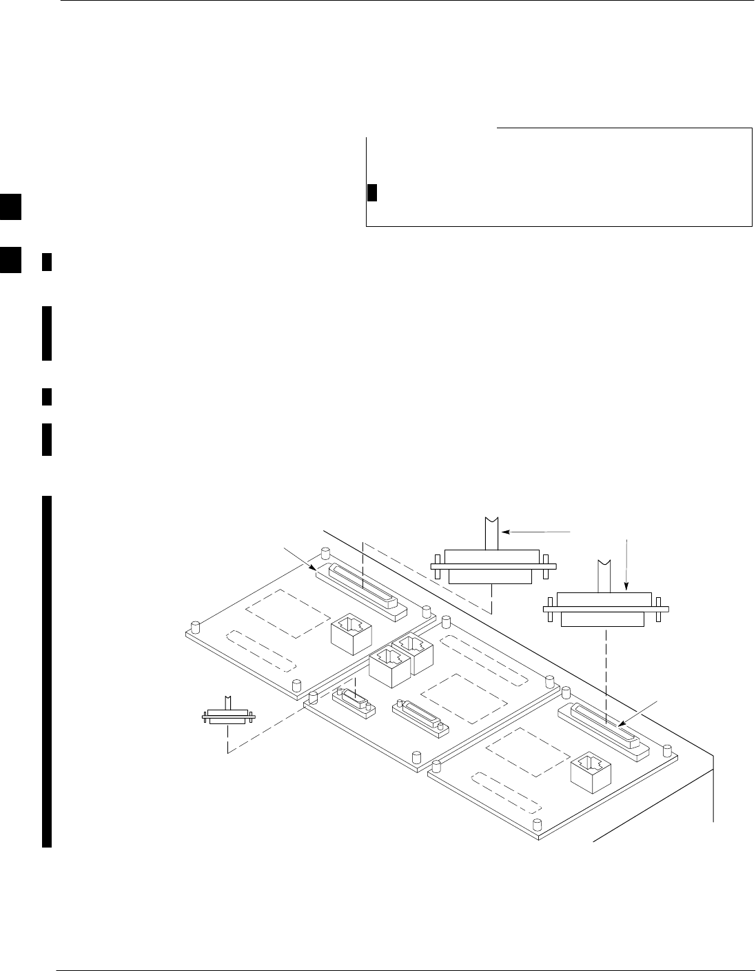
Span Lines – Interface and Isolation
3-16 1X SC 4812T Lite BTS Optimization/ATP FEB 2005
PRELIMINARY
T1/E1 Span Interface
At active sites, the OMC–R/CBSC must disable the BTS
and place it out of service (OOS). DO NOT remove the
Span Line Cable Connectors until the OMC–R/CBSC has
disabled the BTS.
NOTE
Before connecting the LMF Computer to the BTS Frame LAN, the
OMC–R/CBSC must disable the BTS and place it OOS. This will allow
the LMF to control the BTS, and prevent the CBSC from inadvertently
sending Control Information to the BTS during LMF–based Tests.
Isolate the BTS from the T1/E1
Span(s)
Once the OMC–R/CBSC has disabled the BTS, the Span(s) must be
disabled to ensure the LMF will maintain control of the BTS. To disable
the Spans, disconnect the BTS–to–CBSC Transcoder Span Cable
Connectors from the Span I/O Cards (Figure 3-2).
50–PIN TELCO
CONNECTORS
REMOVED
SPAN B CONNECTOR
(TELCO) INTERFACE
TO SPAN LINES
(IF USED
SPAN A CONNECTOR
(TELCO) INTERFACE
TO SPAN LINES
TOP of Frame
(Site I/O and Span I/O Boards)
RS–232 9–PIN SUB D
CONNECTOR SERIAL
PORT FOR EXTERNAL
DIAL UP MODEM
CONNECTION (IF USED)
FW00299 REF
Figure 3-2: Span I/O Board T1 Span Isolation
3

Span Lines – Interface and Isolation – continued
FEB 2005 1X SC 4812T Lite BTS Optimization/ATP 3-17
PRELIMINARY
T1/E1 Span Isolation
Table 3-5 describes the action required for Span Isolation.
Table 3-5: T1/E1 Span Isolation Procedure
nStep Action
1Have the OMC–R/CBSC place the BTS OOS.
2To disable the Span Lines, locate the Connector for the Span or Spans that must be disabled and
remove the respective connector from the applicable SCCP Cage Span I/O Board (Figure 3-2). 3
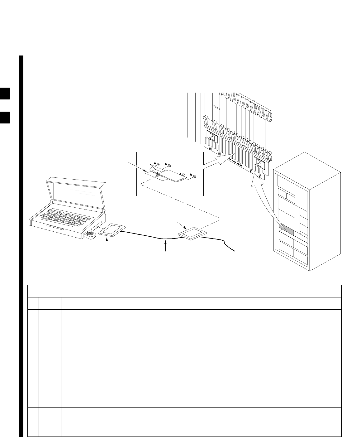
LMF to BTS Connection
3-18 1X SC 4812T Lite BTS Optimization/ATP FEB 2005
PRELIMINARY
Connect the LMF to the BTS
The LMF Computer may be connected to the LAN A or B Connector
located behind the BTS Frame Lower Air Intake Grill. Figure 3-3 shows
the general location of these connectors. LAN A is considered the
Primary LAN.
10BaseT/10Base2
Converter Connects
Directly to BNC T
LMF BNC “T” Connections on
left side of the frame
(Ethernet “A” shown; Ethernet
“B” covered with
hook–and–loop fabric)
LMF Computer
Terminal with Mouse
PCMCIA Ethernet
Adpater & Ethernet
UTP Adapter
Universal Twisted
Pair (UTP) cable
(RJ11 Connectors)
115 VAC Power
Connection
NOTE:
Open LAN CABLE ACCESS door.
Pull apart hook–and–loop fabric
and gain access to the LAN A or
LAN B LMF BNC Connector.
ti-CDMA-WP-00232-v01-ildoc-ftw
SC 4812T LITE
Figure 3-3: LMF Connection Detail
Table 3-6: LMF– to –BTS Connection Procedure
nStep Action
1To gain access to the LAN Connectors, open the LAN Cable Access Door, then pull apart the
fabric covering the BNC “T” Connector and slide out the Service Tray, if desired.
– Refer to Figure 3-3.
2Connect the LMF Computer to the LAN A (left–hand) BNC Connector by using a PCMCIA
Ethernet Adapter.
NOTE
Xircom Model PE3–10B2 or equivalent can also be used to interface the LMF Ethernet
Connection to the BTS Frame connected to the PC Parallel Port, powered by an External AC/DC
Transformer.
– In this case, the BNC Cable must not exceed 91 cm (3 ft) in length.
* IMPORTANT
The LAN Shield is isolated from the Chassis Ground. The LAN Shield (exposed portion of the
BNC Connector) must not touch the chassis during Optimization.
3
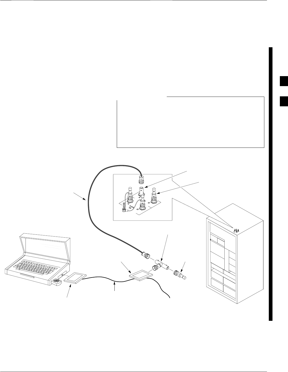
LMF to BTS Connection – continued
FEB 2005 1X SC 4812T Lite BTS Optimization/ATP 3-19
PRELIMINARY
Connect the LMF to the BTS at
the I/O Panel
On BTS Frames produced after May 2004, the LMF must be connected
to the BTS 10Base–2 LAN at the LAN A or B OUT Connectors on the
Frame I/O Panel. Figure 3-4 shows the locations and marking for the I/O
Panel LAN Connectors. This procedure may also be used to connect the
LMF to earlier production frames. LAN A is considered to be the
Primary LAN.
BTS Frames produced after May 2004 do not have a
Service Shelf below the SCCP Cage. As a result, the
COAXial Cable used to connect the LMF Computer with
the I/O Panel LAN Connector must be long enough to
permit placing the LMF Computer in another location
during Optimization or Acceptance Testing.
NOTE
Figure 3-4: I/O Panel LAN Connection
10Base–T/10Base–2
Converter or Hub
Connects Directly
to BNC “T”
LMF Computer
Platform with Mouse
PCMCIA or Built–in
Ethernet Network
Interface Card (NIC)
(10Base–T)
Unshielded Twisted
Pair (UTP) cable
(RJ45 connectors) 115 VAC Power
Connection
(if required)
ti-CDMA-WP-00232-v01-ildoc-ftw
SC 4812T LITE
50 Ω Termination
removed from I/O
panel LAN OUT
connector
BNC “T”
(Jack–Plug–Jack)
COAXial Cable
with two BNC
Plugs
LAN A OUT
Connector
LAN B OUT Connector
(with 50 Ω Termination)
3

LMF to BTS Connection – continued
3-20 1X SC 4812T Lite BTS Optimization/ATP FEB 2005
PRELIMINARY
Table 3-7: Connecting the LMF to the BTS, I/O Panel LAN Connection
nStep Action
1Connect the LMF Computer Platform Network Interface Card (NIC) to the 10Base–2/10Base–T
Converter or Hub.
2Connect a Jack–Plug–Jack Configuration BNC “T” Connector to the 10Base–2/10Base–T
Converter or Hub (Figure 3-4).
3Connect one BNC Plug of the COAXial Cable to one Jack of the BNC “T” Connector.
4* IMPORTANT
1. In this step, do not disconnect the 50 Ω Terminator from either LAN IN Connector on the I/O
Panel (these terminations may be grounded with a Jumper Wire which is fastened to the I/O
Panel).
2. When this step is performed, the active 10Base–2 LAN will swap to the one with the
terminated LAN OUT Connector (LAN B in Figure 3-4).
At the top of the frame, remove the 50 Ω Terminator from one LAN OUT Connector on the I/O
Panel, and connect the remaining BNC Plug on the COAXial Cable to this LAN OUT Connector.
5Connect the 50 Ω Terminator removed in Step 4, above, to the other jack of the BNC “T”
Connector on the Converter or Hub.
6At the I/O Panel, remove the 50 Ω Terminator from the other LAN OUT Connector, and wait 30
seconds for the active LAN to swap to the one connected to the BNC “T”.
7Replace the 50 Ω Terminator on the LAN OUT Connector from where it was removed in Step 6,
above.
3

Switching the Active LAN – LMF I/O Panel 10Base–2 LAN Connection
FEB 2005 1X SC 4812T Lite BTS Optimization/ATP
PRELIMINARY
3-21
Switching the Active LAN
When the LMF Computer is connected to the BTS at the I/O Panel
10Base–2 LAN Connectors, switching the INS_ACT GLI Card to
another LAN (Active LAN Swap) requires more operator actions than
with a Service Shelf LMF Connection. Follow the procedure in
Table 3-8 to force the active LAN Swap with this type of connection.
This procedure is written so it can be used starting with
either LAN A or LAN B.
NOTE
Table 3-8: Forcing an Active 10Base–2 LAN Swap with LMF I/O Panel Connection
nStep Action
1With the LMF Computer connected to a 10Base–2 LAN at the I/O Panel, force the INS_ACT GLI
Card to swap to the other 10Base–2 LAN by performing the following actions.
– Refer to Figure 3-4.
1a Disconnect the LMF COAXial Cable from the I/O Panel LAN OUT Connector.
1b Remove the 50Ω Terminator from the BNC “T” Connector at the 10Base–T/10Base–2 Converter
or Hub (Figure 3-4).
1c Install the 50Ω Terminator on the I/O Panel LAN OUT Oonnector from where the COAXial
Cable was removed in Step 1a, above.
1d Wait approximately 15 seconds.
1e Remove the 50Ω Terminator from the other I/O Panel LAN OUT Connector, and install it on the
open jack of the BNC “T” Connector at the 10Base–T/10Base–2 Converter or Hub (Figure 3-4).
1f Connect the COAXial Cable to the LAN OUT Connector from which the 50Ω Terminator was
removed in Step 1e, above.
1g Wait approximately 15 seconds.
2If applicable, return to the procedure that required performing this operation.
3If not directed to this operation from another procedure, briefly remove and then replace the 50Ω
Terminator on the I/O Panel LAN IN Connector for the LAN from which the LMF was
disconnected in Step 1a, above.
4Verify the LAN is active by pinging the processor of the INS_ACT GLI Card using the procedure
in Table 3-15.
3