Nokia Solutions and Networks T6FE1 PCS Licensed Transmitter User Manual 68P09262A58 C
Nokia Solutions and Networks PCS Licensed Transmitter 68P09262A58 C
Contents
- 1. User Manual 1 of 3
- 2. User Manual 2 of 3
- 3. User Manual 3 of 3
User Manual 2 of 3

Using the LMF
3-22 1X SC 4812T Lite BTS Optimization/ATP FEB 2005
PRELIMINARY
Basic LMF Operation
LMF Coverage in this Publication
The LMF Application Program supports maintenance of both CDMA
and SAS BTSs. All references to the LMF in this publication are to the
CDMA portion of the program..
Operating Environments
The LMF Application Program allows the user to work in the two
following Operating Environments that are accessed using the specified
Desktop Icons.:
– Graphical User Interface (GUI) using the WinLMF Icon
– Command Line Interface (CLI) using the WinLMF CDMA CLI
Icon
The GUI is the primary Optimization and Acceptance Testing Operating
Environment. The CLI Environment provides additional capability to the
user to perform manually controlled Acceptance Tests and audit the
results of Optimization and Calibration Actions.
Basic Operation
Basic Operation of the LMF in either environment includes performing
the following tasks.:
SSelecting and deselecting BTS Devices
SEnabling Devices
SDisabling Devices
SResetting Devices
SObtaining Device Status
The following additional Basic Operation can be performed in a GUI
Environment:
SSorting a Status Report Window
For detailed information on performing these and other LMF Operations,
refer to the LMF Help function on–line documentation.
Unless otherwise noted, LMF procedures in this manual
are performed using the GUI Environment.
NOTE
The LMF Display and the BTS
BTS Display
When the LMF is logged into a BTS, a Frame Tab is displayed for each
BTS Frame. The Frame Tab is labeled with “CDMA” and the BTS
Number, a Dash, and the Frame Number (for example, BTS–812–1 for
BTS 812, RF Modem Frame 1). If there is only one frame for the BTS,
there will only be one Frame Tab..
3

Using the LMF – continued
FEB 2005 1X SC 4812T Lite BTS Optimization/ATP 3-23
PRELIMINARY
CDF/NECF Requirements
For the LMF to recognize the devices installed in the BTS, a BTS
CDF/NECF File that includes Equipage Information for all the devices
in the BTS must be located in the applicable <x>:\<lmf Home
Directory>\cdma\bts–# folder. To provide the necessary Channel
Assignment Data for BTS Operation, a CBSC CDF File that includes
Channel Data for all BTS RF Modem Frames is also required in the
folder..
RFDS Display
If an RFDS is included in the CDF/NECF File, an RFDS Tab labeled
with “RFDS,” a Dash, and the BTS Number–Frame Number
Combination (for example, RFDS–812–1) is displayed..
Graphical User Interface
Operation
Perform the procedure in Table 3-9 to operate the LMF GUI.
Table 3-9: LMF GUI Operating Procedure
nStep Action
1Select the device or devices upon which an action is to be performed.
2Select the action to apply to the selected device(s).
– While the action is in progress, a Status Report Window displays the action taking place and
other status information.
– When the action is complete, the Status Report Window states its completion and displays
other pertinent information.
3Click the OK Button to close the Status Report Window.
3
Using the LMF – continued
3-24 1X SC 4812T Lite BTS Optimization/ATP FEB 2005
PRELIMINARY
Understanding GUI Operation
The following Screen Captures are provided to help understand how the
GUI operates. For detailed information on performing these and other
LMF Operations, refer to the LMF Help function on–line documentation.
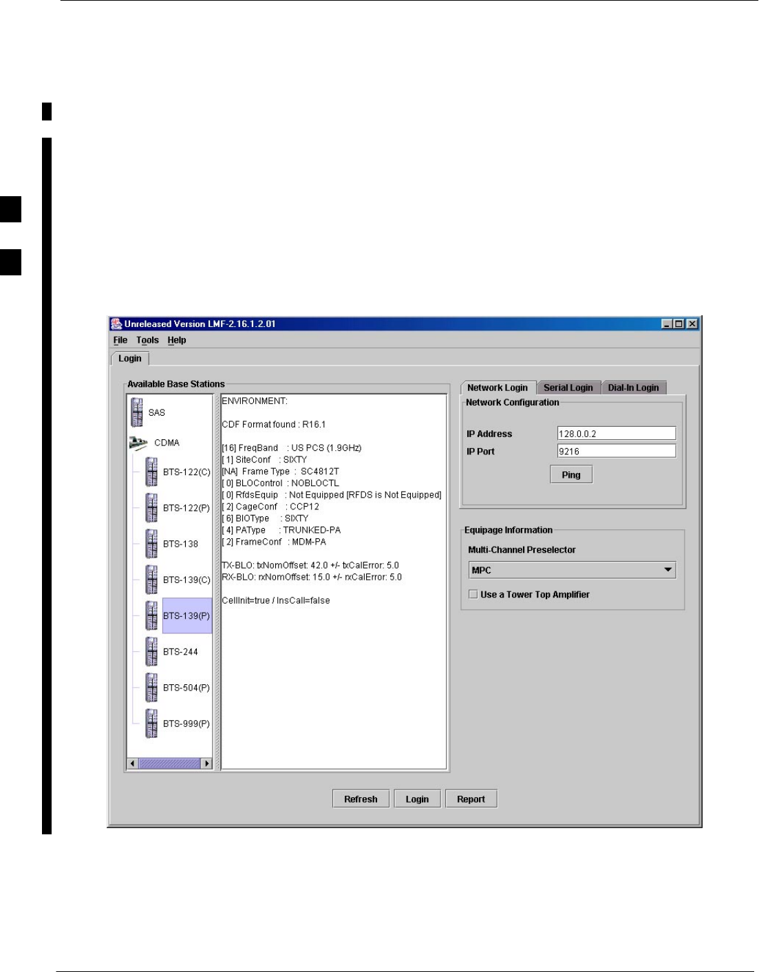
BTS Login Screen
Figure 3-5 depicts the differences between Packet and Circuit CDMA
“cdf” File Identification. Note that if there is a Packet Mode Version
“bts” File, the “(P)” is added as a suffix. There is a corresponding “(C)”
for the Circuit Mode Version.
Figure 3-5: BTS Login Screen – Identifying Circuit and Packet BTS Files
3
Using the LMF – continued
FEB 2005 1X SC 4812T Lite BTS Optimization/ATP 3-25
PRELIMINARY
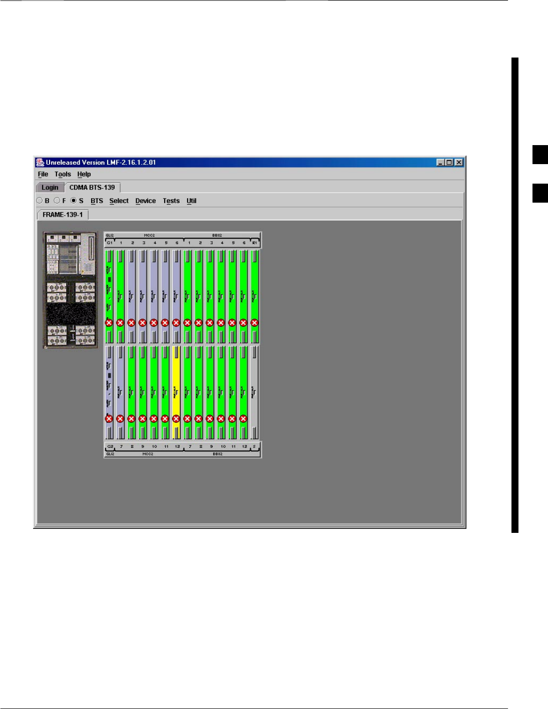
Self-Managed Network Elements Screen
Figure 3-6 depicts the Self-Managed Network Elements (NEs) State of a
Packet Mode SC4812T. Note that an “X” is on the front of each card that
is under Self–Managed Network Elements (NEs) Control by the GLI3
Card.
Figure 3-6: Self–Managed Network Elements (NEs) State of a Packet Mode SC4812T
3
Using the LMF – continued
3-26 1X SC 4812T Lite BTS Optimization/ATP FEB 2005
PRELIMINARY
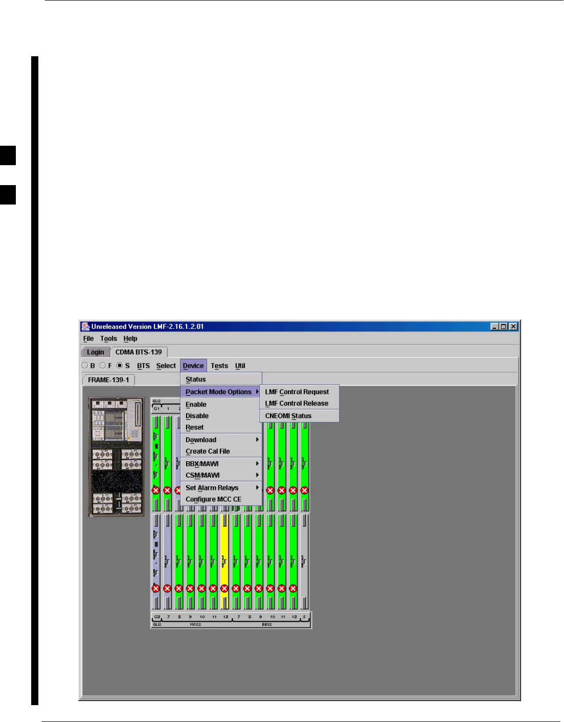
Packet Mode Commands Screen
Figure 3-7 depicts three of the available Packet Mode Commands.
Normally the GLI3 has Self-Managed Network Elements (NEs) Control
of all cards as shown in Figure 3-6 by an “(X)”. In that state, the LMF
may only status a single card.
In order to download code or test a card, the LMF must request
Self-Managed Network Elements (NEs) Control of the card by using the
shown Pull–down Menu. It also uses this menu to release control of the
card back to the GLI3.
The GLI3 also assumes control of the cards after the LMF logs out of the
BTS. The Packet Mode GLI3 normally is loaded with a Tape Release
and NECB and NECJ Files that point to a Tape Release stored on the
GLI3. When the GLI3 has control of a card it will maintain that card
with the code on that Tape Release.
Figure 3-7: Available Packet Mode Commands
3
Using the LMF – continued
FEB 2005 1X SC 4812T Lite BTS Optimization/ATP 3-27
PRELIMINARY
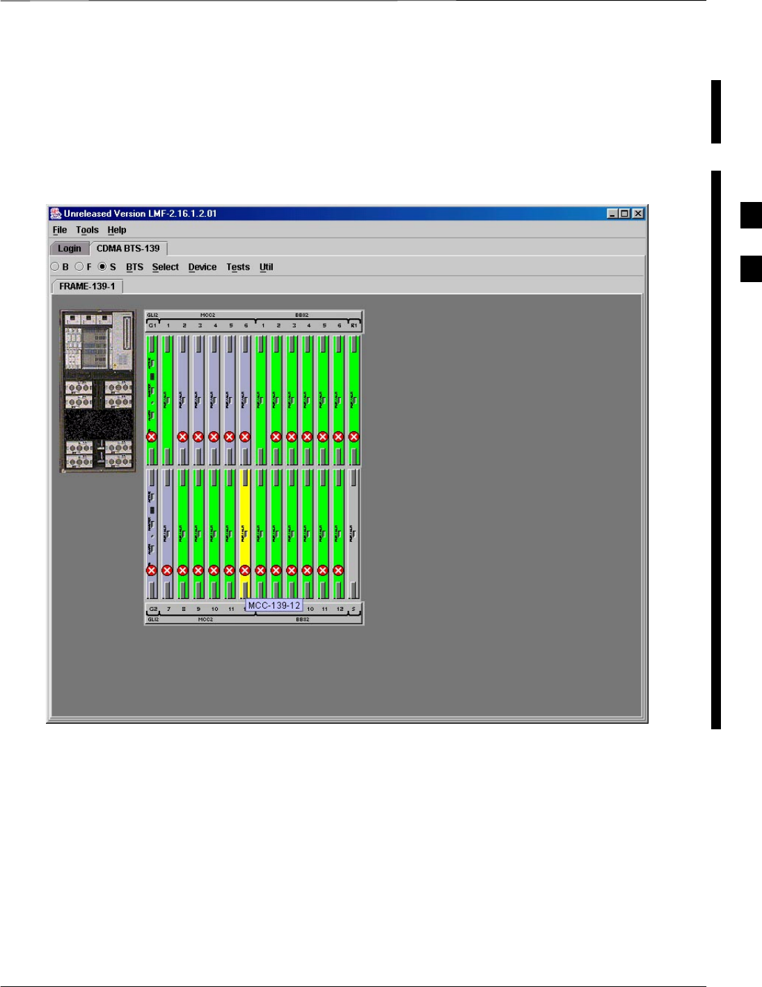
Packet Mode Site under LMF Control
Figure 3-8 depicts a Packet Mode Site that has the MCC–1 and the
BBX–1 Cards under LMF Control. Notice that the “X” is missing from
the front of these two cards.
Figure 3-8: Packet Mode Site with MCC–1 and BBX–1 under LMF Control
3

Using the LMF – continued
3-28 1X SC 4812T Lite BTS Optimization/ATP FEB 2005
PRELIMINARY
Command Line Interface
Overview
The LMF also provides Command Line Interface (CLI) capability.
Activate the CLI by clicking on a Shortcut Icon on the Desktop. The CLI
can not be launched from the GUI, only from the Desktop Icon.
Both the GUI and the CLI use a program known as the Handler. Only
one Handler can be running at one time. The architectural design is such
that the GUI must be started before the CLI if you want the GUI and CLI
to use the same Handler.
When the CLI is launched after the GUI, the CLI automatically finds and
uses an in–progress Login Session with a BTS initiated under the GUI.
This allows the use of the GUI and the CLI in the same BTS Login
Session.
If a CLI Handler is already running when the GUI is launched (this
happens if the CLI Window is already running when the user starts the
GUI, or if another copy of the GUI is already running when the user
starts the GUI), a Dialog Window displays the following Warning
Message:
The CLI Handler is already running.
This may cause conflicts with the LMF.
Are you sure that you want to start the application?
This window also contains YES and NO Buttons.
– Selecting YES starts the application.
– Selecting NO terminates the application.
CLI Format Conventions
The CLI Command can be broken down in the following way:
SVerb
SDevice including Device Identifier Parameters
SSwitch
SOption Parameters consisting of:
– Keywords
– Equals Sign (=) between the Keyword and the Parameter Value
– Parameter Values
Spaces are required between the verb, device, switch, and option
parameters. A hyphen is required between the device and its identifiers.
Following is an example of a CLI Command.
measure bbx–<bts_id>–<bbx_id> rssi channel=6–Sector=5
Refer to the LMF CDMA CLI Reference (68P09262A25) for a complete
explanation of the CLI Commands and their usage.
Logging Into a BTS
Logging into a BTS establishes a Communication Link between the BTS
and the LMF. An LMF Session can be logged into only one BTS at a
time.
3
Using the LMF – continued
FEB 2005 1X SC 4812T Lite BTS Optimization/ATP 3-29
PRELIMINARY
Prerequisites
Before attempting to log into a BTS, ensure that the following tasks have
been completed:
SThe LMF Program is correctly installed on the LMF Computer.
SA bts-nnn Folder with the correct CDF/NECF and CBSC Files is
present.
SThe LMF Computer was connected to the BTS before starting the
Windows Operating System and the LMF Software. If necessary,
restart the computer after connecting it to the BTS in accordance with
Table 3-6 and Figure 3-3.
Ensure that the correct bts–#.cdf/necf and cbsc–#.CDF
Files are used for the BTS. These should be the
CDF/NECF Files that are provided for the BTS by the
CBSC.
Failure to use the correct CDF/NECF Files can result in
invalid Optimization.
Failure to use the correct CDF/NECF Files to log into
a live (traffic–carrying) site can shut down the site.
CAUTION
BTS Login from the GUI Environment
Perform the procedure in Table 3-10 to log into a BTS when using the
GUI Environment.
Table 3-10: BTS GUI Login Procedure
nStep Action
1Start the LMF GUI Environment by double–clicking on the WinLMF Desktop Icon (if the LMF is
not running).
– An LMF Window will open and display the LMF Build Number in the Title Bar.
2If a warning similar to the following is displayed, proceed to Step 3.
The CLI Handler is already running.
This may cause conflicts with the LMF.
Are you sure you want to start the application?
Yes No
table continued on next page
3

Using the LMF – continued
3-30 1X SC 4812T Lite BTS Optimization/ATP FEB 2005
PRELIMINARY
Table 3-10: BTS GUI Login Procedure
nActionStep
* IMPORTANT
The following statements are provided to assist the operator in using the LMF GUI.
SIf an attempt is made to log into a BTS that is already logged on, all devices will appear gray in
the display.
SThere may be instances where the BTS initiates a log out due to a system error (i.e., a device
failure).
SIf the MGLI is OOS–ROM (blue in the display), it must be downloaded with RAM Code before
other devices can be seen.
SIf the MGLI is OOS–RAM (yellow in the display), it must be enabled before other installed
devices can be seen.
3Perform the following actions:
3a Select NO.
3b Shut down any other LMF Sessions that may be running.
3c Start the LMF GUI Environment again.
4Click on the Login Tab (if not displayed).
5Double click on CDMA (in the Available Base Stations Pick List).
6Click on the desired BTS Number.
7Click on the Network Login Tab (if not already in the forefront).
8Enter the correct IP Address (normally 128.0.0.2) for a Customer BTS, if not correctly displayed
in the IP Address Box.
9Enter the correct IP Port Number (normally 9216), if not correctly displayed in the IP Port Box.
10 Click on Ping.
SIf the connection is successful, the Ping Display Window shows text similar to the following:
Reply from 128.0.0.2: bytes=32 time=3ms TTL=255
SIf there is no response, the following is displayed:
128.0.0.2:9216:Timed out
SIf the MGLI fails to respond, reset and perform the Ping Process again.
SIf the MGLI still fails to respond, check for the following problems:
– Shorted BNC to Inter–frame Cabling
– Open Cables
– Crossed A and B Link Cables
– Missing 50–Ohm Terminators
– MGLI problem
table continued on next page
3
Using the LMF – continued
FEB 2005 1X SC 4812T Lite BTS Optimization/ATP 3-31
PRELIMINARY
Table 3-10: BTS GUI Login Procedure
nActionStep
11 In the Equipage Information Field, select the Multi-channel Preselector Type from the
Multi-channel Preselector Pull–down Menu (default is MPC) to a device corresponding to your
BTS Configuration, if required.
NOTE
The “Use a Tower Top Amplifier” Option is not applicable to the SC4812T Lite.
12 In the SC4812ET Lite/T Lite Field, click in the SC4812T Lite Check Box to select it.
NOTE
This Check Box is used to differentiate the SC4812ET Lite BTS Frame from the SC4812T Lite
BTS Frame.
13 Click on Login.
– A BTS Tab with the BTS and Frame Numbers is displayed.
3
Using the LMF – continued
3-32 1X SC 4812T Lite BTS Optimization/ATP FEB 2005
PRELIMINARY
BTS Login from the CLI Environment
Perform the procedures in Table 3-11 to log into a BTS when using the
CLI Environment.
If the CLI and GUI Environments are to be used at the
same time, the GUI must be started first and the BTS
Login must be performed from the GUI.
– Refer to Table 3-10 to start the GUI Environment and
log into a BTS.
NOTE
Table 3-11: BTS CLI Login Procedure
nStep Action
1Double–click the WinLMF CLI Desktop Icon (if the LMF CLI Environment is not already
running).
NOTE
If a BTS was logged into under a GUI Session before the CLI Environment was started, the CLI
Session will be logged into the same BTS, and Step 2 is not required.
2At the /wlmf Prompt, enter the following command:
Login bts–<bts#> host=<host> port=<port> tlite
where:
–host = MGLI Card IP Address (defaults to address last logged into for this BTS or 128.0.0.2,
if this is first Login to this BTS).
–port = IP Port of the BTS (defaults to the port last logged into for this BTS, or 9216 if this is
first Login to this BTS).
–tlite = option used to differentiate between SCCP Cage BTS Models (i.e. SC4812ET Lite
AND SC4812T Lite).
– A response similar to the following will be displayed:
LMF>
13:08:18.882 Command Received and Accepted
COMMAND=Login bts–33
13:08:18.882 Command In Progress
13:08:21.275 Command Successfully Completed
REASON_CODE=”No Reason”
3

Using the LMF – continued
FEB 2005 1X SC 4812T Lite BTS Optimization/ATP 3-33
PRELIMINARY
Logging Out
Logging out of a BTS is accomplished differently for the GUI and CLI
Operating Environments.
The GUI and CLI Environments use the same connection
to a BTS.
– If a GUI and the CLI Session are running for the
same BTS at the same time, logging out of the BTS
in either environment will log out of it for both.
When either a Login or logout is performed in the CLI
Window, there is no GUI indication that the Login or
Logout has occurred.
NOTE
Logging Out of a BTS from the GUI Environment
Perform the procedure in Table 3-12 to logout of a BTS when using the
GUI Environment.
Table 3-12: BTS GUI Logout Procedure
nStep Action
1Click on BTS in the BTS Menu Bar.
2Click the Logout item in the Pull–down Menu (a Confirm Logout Pop-up Message will appear).
3Click on Yes (or press the Enter Key) to confirm logout.
– The Login Tab will appear.
SIf a logout was previously performed on the BTS from a CLI Window running at the same time
as the GUI, a Logout Error Pop–up Message will appear stating that the system could not log
out of the BTS. When this occurs, the GUI must be exited and restarted before it can be used for
further operations.
SIf a Logout Error Pop–up Message appears stating that the system could not log out of the
Base Station because the given BTS is not logged in, click OK and proceed to Step 4.
4 Select File > Exit in the Window Menu Bar, click Yes in the Confirm Logout Pop–up Window.
5 Click OK in the Logout Error Pop–up Window that appears again.
6If further work is to be done in the GUI, restart it.
NOTE
SThe Logout item on the BTS Menu Bar will only log you out of the displayed BTS.
SYou can also log out of all BTS Sessions and exit LMF by clicking on the File Selection in the
Menu Bar and selecting Exit from the File Menu List.
–A Confirm Logout Pop–up Message will appear.
3

Using the LMF – continued
3-34 1X SC 4812T Lite BTS Optimization/ATP FEB 2005
PRELIMINARY
Logging Out of a BTS from the CLI Environment
Perform the procedure in Table 3-13 to logout of a BTS when using the
CLI Environment.
Table 3-13: BTS CLI Logout Procedure
nStep Action
NOTE
If the BTS is also logged into from a GUI running at the same time and further work must be done
with it in the GUI, proceed to Step 1.
1Log out of a BTS by entering the following command:
logout bts–<bts#>
– A system response similar to the following will be displayed:
LMF>
13:24:51.028 Command Received and Accepted
COMMAND=logout bts–33
13:24:51.028 Command In Progress
13:24:52.04 Command Successfully Completed
REASON_CODE=”No Reason”
2If desired, close the CLI Interface by entering the following command:
exit
– A response similar to the following will be displayed before the window closes:
Killing background processes....
Establishing an MMI
Communication Session
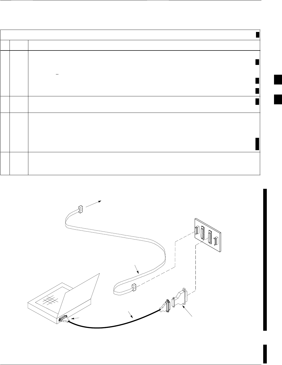
Equipment Connection
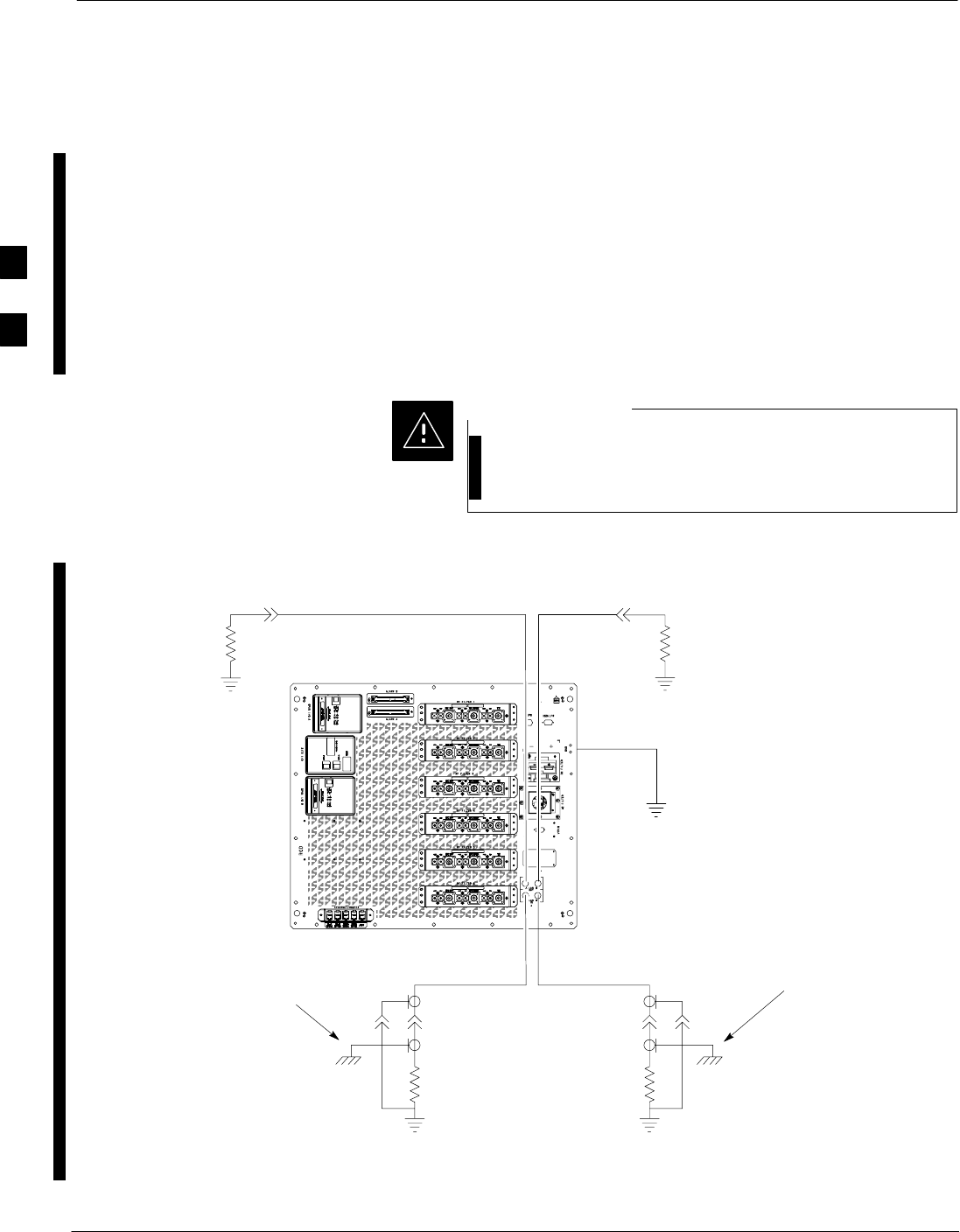
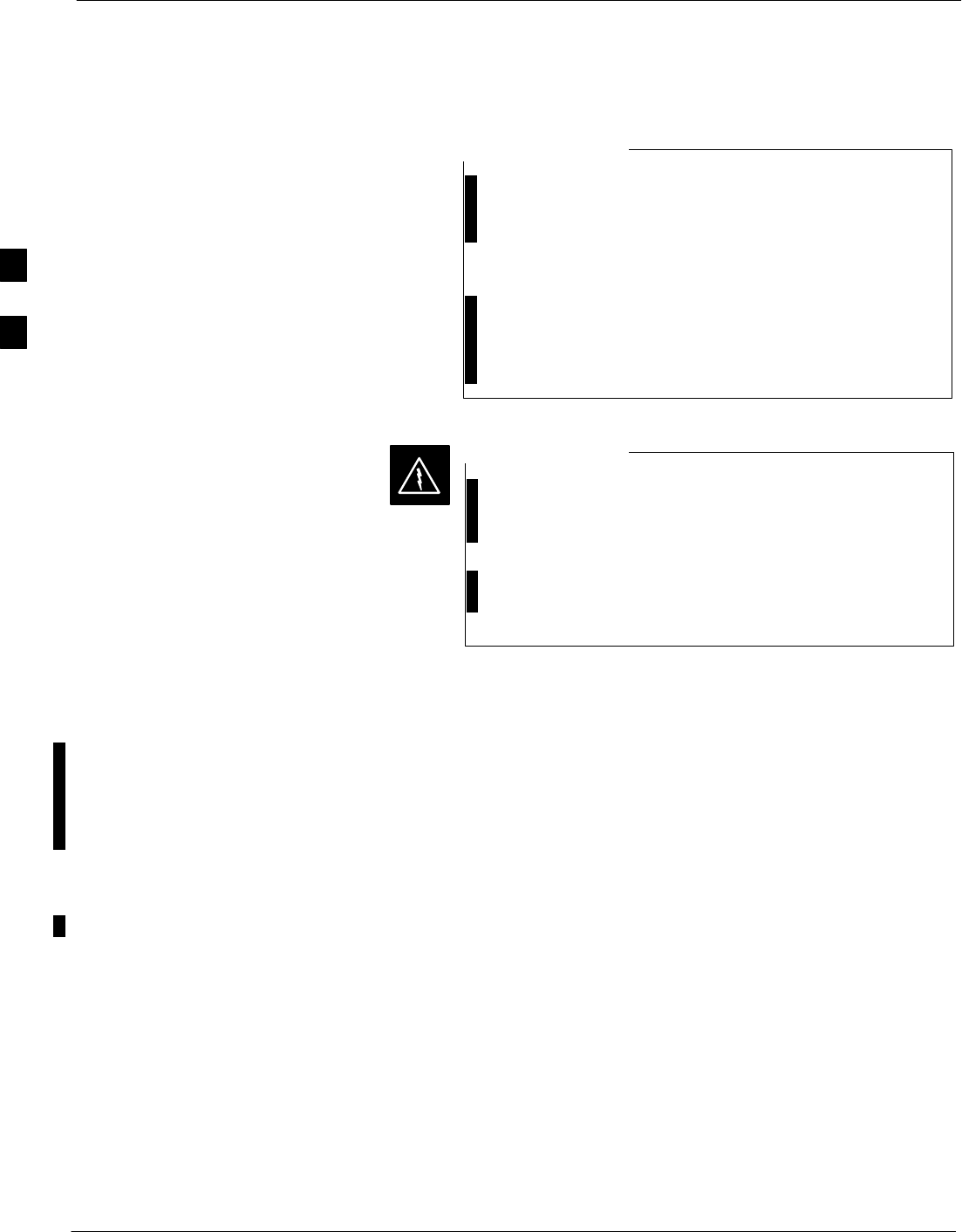
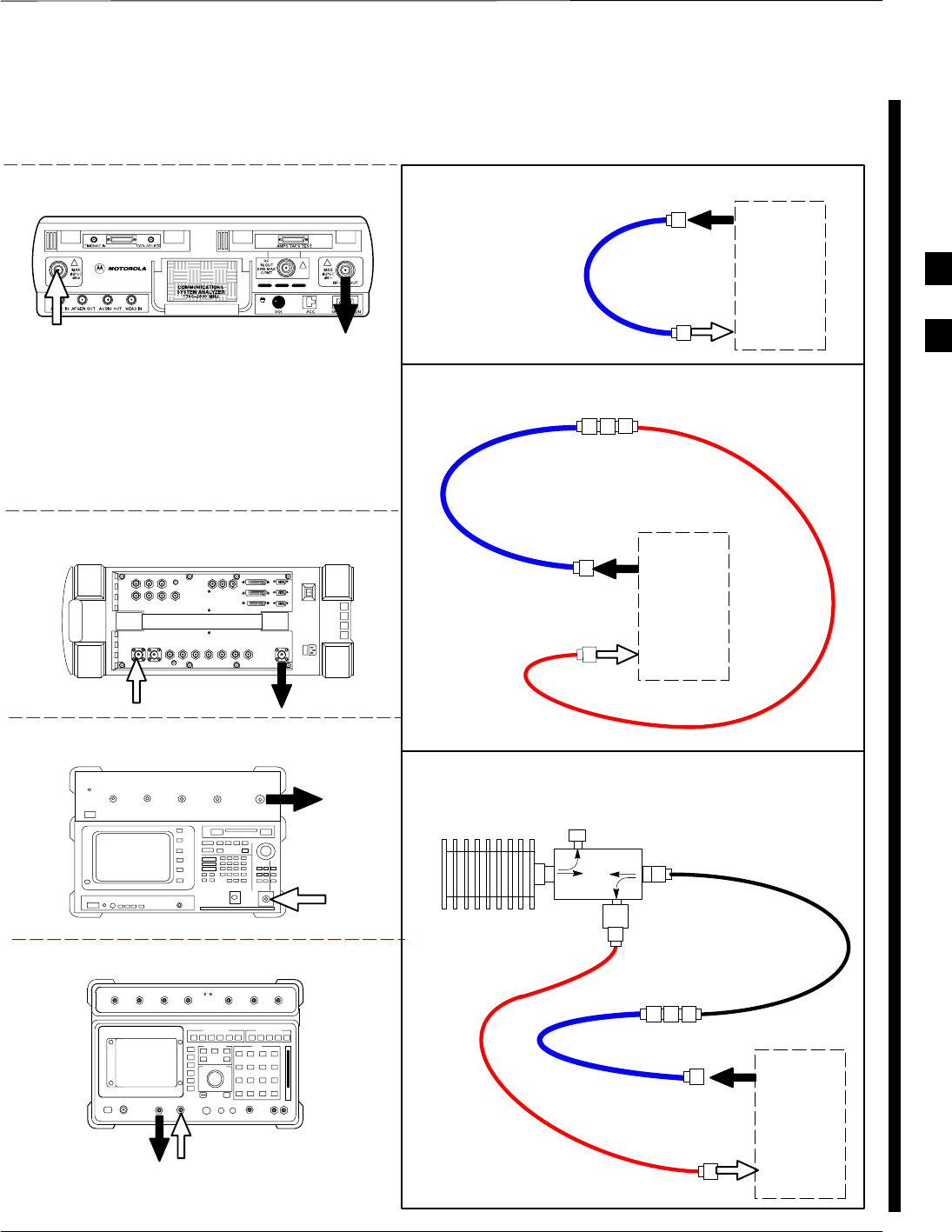
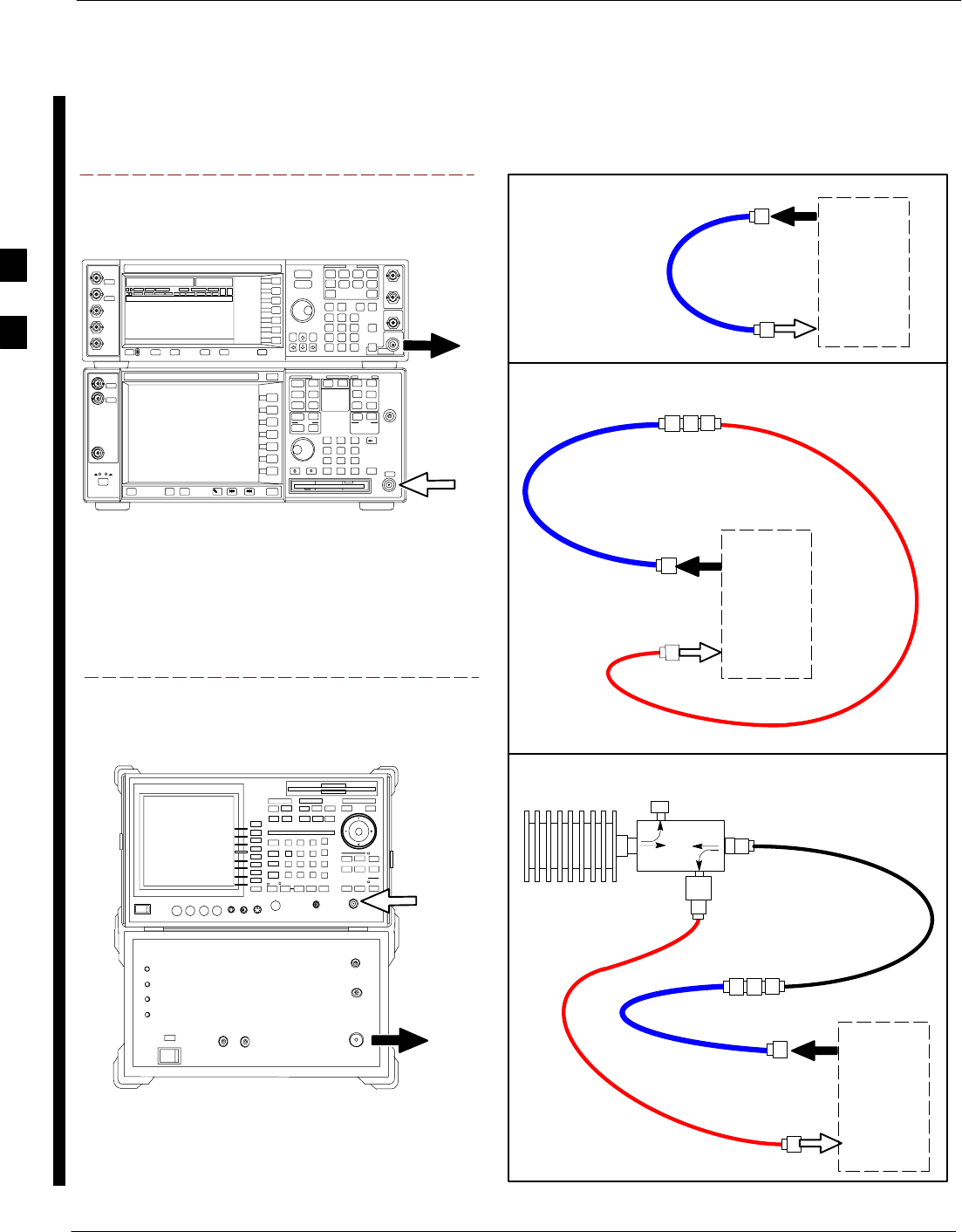
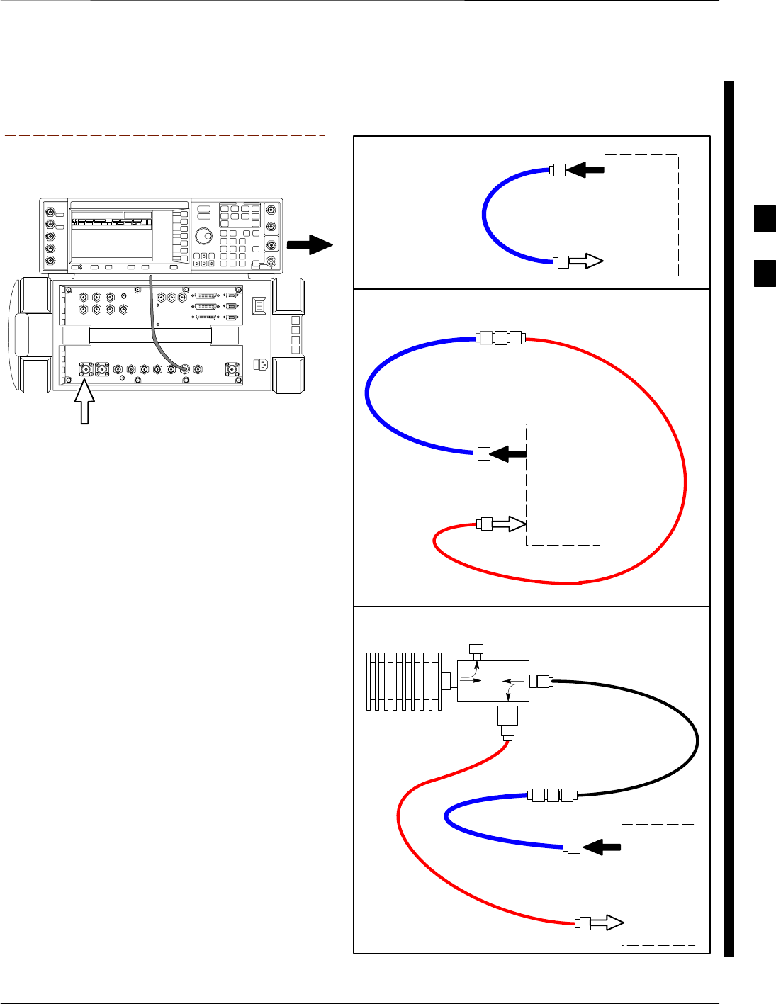
Figure 3-9 illustrates common equipment connections for the LMF
Computer. For specific connection locations on FRUs, refer to the
illustration accompanying the procedures that require the MMI
Communication Session..
Initiate MMI Communication
For those procedures that require MMI Communication between the
LMF and BTS FRUs, perform the procedures in Table 3-14 to initiate
the Communication Session..
Table 3-14: Establishing MMI Communication Procedure
nStep Action
1Connect the LMF Computer to the equipment as detailed in the applicable procedure that requires
the MMI Communication Session.
table continued on next page
3
Using the LMF – continued
FEB 2005 1X SC 4812T Lite BTS Optimization/ATP 3-35
PRELIMINARY
Table 3-14: Establishing MMI Communication Procedure
nActionStep
2If the LMF Computer has only one Serial Port (COM1) and the LMF is running, disconnect the
LMF from COM1 by performing the following actions.
2a Click on Tools in the LMF Window Menu Bar, and select Options from the Pull–down Menu.
– An LMF Options Dialog Box will appear.
2b In the LMF Options Dialog Box, click the Disconnect Port Button on the Serial Connection Tab.
3Start the named HyperTerminal Connection for MMI Sessions by double clicking on its Windows
Desktop Shortcut.
NOTE
If a Windows Desktop Shortcut was not created for the MMI Connection, access the connection
from the Windows Start Menu by selecting:
Programs > Accessories > Hyperterminal > HyperTerminal > <Named HyperTerminal
Connection (e.g., MMI Session)>
4Once the MMI Connection Window opens, establish MMI Communication with the BTS FRU by
pressing the LMF Computer <Enter>Key until the prompt identified in the applicable procedure
is obtained.
NULL MODEM
BOARD
(TRN9666A)
8–PIN TO 10–PIN
RS–232 CABLE
(P/N 30–09786R01)
RS–232 CABLE
8–PIN
LMF
COMPUTER
To FRU MMI Port
DB9–TO–DB25
ADAPTER
COM1
OR
COM2
FW00687
Figure 3-9: LMF Computer Common MMI Connections
Online Help
Task oriented Online Help is available in the LMF by clicking Help in
the Window Menu Bar, and selecting LMF Help from the Pull–down
Menu.
3
Pinging the Processors
3-36 1X SC 4812T Lite BTS Optimization/ATP FEB 2005
PRELIMINARY
Pinging the BTS
For proper operation, the integrity of the 10Base–2 Ethernet LAN A and
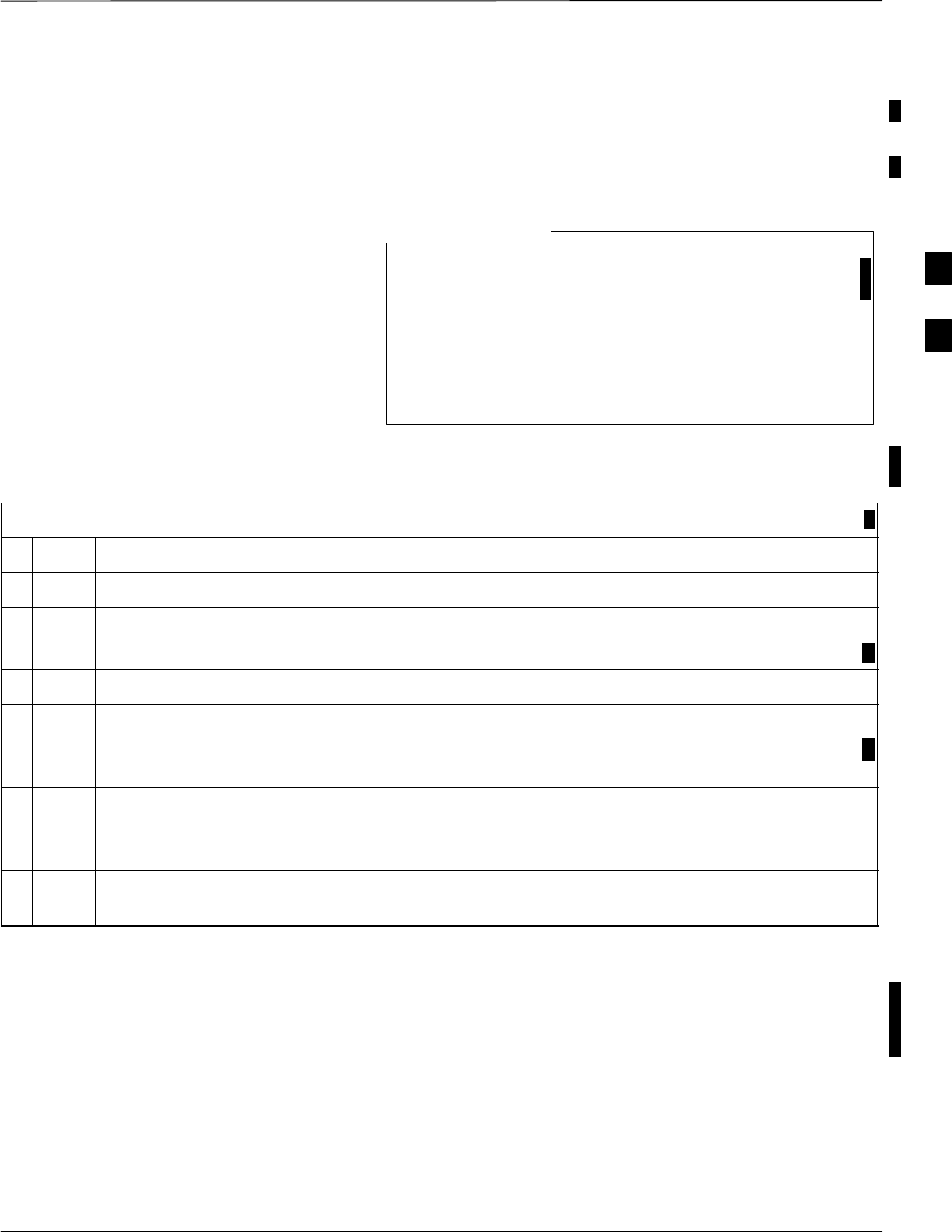
B Links must be verified. Figure 3-10 represents a typical BTS Ethernet
Configuration for an SC4812T Lite Stand–alone Frame. The drawing
depicts cabling and terminators for both the A and B LANs.
”Ping” is a program that sends Request Data Packets to hosts on a
network, in this case GLI Cards on the BTS LAN, to obtain a response
from the “Target” Host specified by an IP Address.
Perform the steps in Table 3-15 to ping each processor (on both LAN A
and LAN B) and verify that LAN Redundancy is working properly.
Always wear an approved Anti–static Wrist Strap while
handling any circuit card/module to prevent damage by
Electrostatic Discharge (ESD).
CAUTION
Figure 3-10: BTS 10base–2 Ethernet LAN Terminator
SIGNAL
GROUND
SIGNAL
GROUND
50Ω
SIGNAL
GROUND
50Ω
50Ω
SIGNAL
GROUND
50Ω
SIGNAL
GROUND
FRAME GROUND
BNC
TERMINATOR
BNC
TERMINATOR
BNC
TERMINATOR
LAN A IN
LAN A OUT
SC4812TL0013–5
BNC
TERMINATOR
SC4812T- Lite
I/O Panel
LAN B IN
LAN B OUT
CHASSIS GROUND
(GROUNDED 50Ω
TERMINATORS)
CHASSIS GROUND
(GROUNDED 50Ω
TERMINATORS)
3

Pinging the Processors – continued
FEB 2005 1X SC 4812T Lite BTS Optimization/ATP 3-37
PRELIMINARY
The Ethernet LAN A and B Cables and/or Terminators
must be installed on each BTS Frame/Enclosure External
LAN Connector before performing this test. All other
Processor Card LAN Connections are made through the
backplanes.
NOTE
Table 3-15: Pinging the Processors Procedure
nStep Action
1If this is a first–time communication with a newly–installed frame or a GLI Card that has been
replaced:
– Perform the procedure in Table 6-4.
– Then, return to Step 2.
2Ensure that any uncabled LAN A and B IN and OUT Connectors are terminated with 50 Ω Loads.
3If it has not already been done, connect the LMF Computer to BNTS LAN A.
– Refer to Table 3-6 and Figure 3-3, or Table 3-7 and Figure 3-4.
4If it has not already been done, start a GUI LMF Session and log into the BTS .
– Refer to Table 3-10.
5At the I/O Panel, remove the 50Ω Terminator on the Frame LAN B IN Connector.
– The LMF session should remain active.
6Replace the 50Ω Terminator on the BTS Frame LAN B IN Connector.
7From the Windows Desktop, click the Start Button and select Run.
8In the Open Box, type ping and the INS_ACTIVE GLI IP Address (for example, ping
128.0.0.2).
NOTE
128.0.0.2 is the Default IP Address for the GLI Card in Slot GLI–1 in operational BTS Units.
9Click on OK.
SIf the targeted GLI Card responds, a DOS Window will appear with a display similar to the
following:
Reply from 128.0.0.2: bytes=32 time=3ms TTL=255
SIf the GLI responds, proceed to Step 19.
SIf there is no response, the following is displayed:
Request timed out
SIf the GLI fails to respond, proceed to Step 10.
table continued on next page
3

Pinging the Processors – continued
3-38 1X SC 4812T Lite BTS Optimization/ATP FEB 2005
PRELIMINARY
Table 3-15: Pinging the Processors Procedure
nActionStep
10 Reset and re–Ping the target MGLI.
SIf the GLI does respond, proceed to Step 19.
SIf the GLI does not respond, typical problems to check are as follows:
– Failure of the LMF to Login.
– Shorted BNC–to–Inter-Frame Cabling
– Open cables
– Crossed A and B Link Cables
– GLI problem
11 Logout of the BTS as described in Table 3-12, exit from the LMF Program, and restart the
Windows Operating System on the LMF Computer.
12 Restart the LMF GUI Program as described in WinLMF On-Line Help SR2.16.x , and log into the
BTS as described in Table 3-10.
13 Perform Step 7 through Step 9 again.
SIf the GLI does respond, proceed to Step 19.
SIf the GLI does not respond, proceed to Step 14.
14 If the Ping Attempt was unsuccessful after restarting the LMF Computer:
– Press the MGLI Front Panel Reset Button.
–Perform Step 7 through Step 9 again.
NOTE
Refer to Table 6-1 if the Ping Attempt was unsuccessful after resetting the MGLI.
15 After the BTS has been successfully pinged, ensure that the 50Ω Terminator is replaced on the
BTS Frame LAN B IN Connector in the Power Entry Compartment (Figure 3-10).
16 Disconnect the LMF Cable from the LAN Shelf LAN A Connector, and connect it to LAN B
(right–hand Connector).
– Refer to Figure 3-3.
17 In the Power Entry Compartment, remove the 50Ω Terminator on the BTS Frame LAN A IN
Connector.
18 Repeat Step 5 through Step 9 using LAN B.
19 After the BTS has been successfully pinged on the Secondary LAN, replace the 50Ω Terminator
on the Frame LAN A IN Connector in the Power Entry Compartment.
20 Disconnect the LMF Cable from the LAN Shelf LAN B and connect it to LAN A.
21 Remove and replace the 50Ω Terminator on the LAN B IN Connector to force the MGLI to switch
to Primary LAN A.
22 Repeat Step 5 through Step 9 to ensure proper Primary LAN Operation.
3

Download the BTS
FEB 2005 1X SC 4812T Lite BTS Optimization/ATP 3-39
PRELIMINARY
Overview
Before a BTS can operate, each equipped device must contain Device
Initialization (ROM) Code. ROM Code is loaded in all devices during
manufacture, factory repair, or, for software upgrades, from the CBSC
using the DownLoad Manager (DLM). Device Application (RAM) Code
and Data must be downloaded to each equipped device by the user
before the BTS can be made fully functional for the site where it is
installed.
ROM Code
Downloading ROM Code to BTS Devices from the LMF is NOT
Routine Maintenance or a normal part of the Optimization Process. It is
only done in unusual situations where the resident ROM Code Release
Level in the device is not compatible with the required Release Level of
the Site Operating Software and the CBSC can not communicate with
the BTS to perform the download.
– If you must download ROM Code, the procedures are located in
Appendix G.
Before ROM Code can be downloaded from the LMF, the correct ROM
Code File for each device to be loaded must be present on the LMF
Computer. ROM Code must be manually selected for download.
The ROM Code File is not available for GLI3s. GLI3s are
ROM Code loaded at the factory.
NOTE
ROM Code can be downloaded to a device that is in any state. After the
download is started, the device being downloaded changes to
OOS_ROM (blue). The device will remain OOS_ROM (blue) when the
download is completed.
A compatible Revision Level RAM Code must then be downloaded to
the device. Compatible Code Loads for ROM and RAM must be used
for the device type to ensure proper performance. The compatible Device
Code Release Levels for the BSS Software Release being used are listed
in the Version Matrix section of the SCt CDMA Release Notes
(supplied on the tape or CD–ROM containing the BSS Software).
RAM Code
Before RAM Code can be downloaded from the LMF, the correct RAM
Code File for each device must be present on the LMF Computer. RAM
Code can be automatically or manually selected depending on the
Device Menu Item chosen and where the RAM Code File for the device
is stored in the LMF File Structure.
3

Download the BTS – continued
3-40 1X SC 4812T Lite BTS Optimization/ATP FEB 2005
PRELIMINARY
The RAM Code File will be selected automatically if the file is in the
<x>:\<lmf Home Directory>\cdma\loads\n.n.n.n\code Folder (where
n.n.n.n is the download Code Version Number that matches the
“NextLoad” Parameter of the CDF File). The RAM Code File in the
Code Folder must have the correct Hardware BIN Number for the device
to be loaded.
RAM Code can be downloaded to a device that is in any state. After the
download is started, the device being loaded changes to OOS_ROM
(blue). When the download is completed successfully, the device
changes to OOS_RAM (yellow).
When code is downloaded to an MGLI or GLI, the LMF also
automatically downloads data and then enables the MGLI. When
enabled, the MGLI changes to INS_ACTIVE (bright green). A
Redundant GLI will not be automatically enabled and will remain
OOS_RAM (yellow). When the Redundant GLI is manually commanded
to enable through the LMF, it changes state to INS_STANDBY (olive
green).
For non–GLI Devices, data must be downloaded after RAM Code is
downloaded. To download data, the Device State must be OOS_RAM
(yellow).
The devices to be loaded with RAM Code and Data are:
SMaster Group Line Interface (MGLI2 or MGLI3)
SRedundant GLI (GLI2 or GLI3)
SClock Synchronization Module (CSM) (Only if new Revision Code
must be loaded)
SMulti–Channel CDMA (MCC24E, MCC8E, or MCC–1X) Cards
SBroadband Transceiver (BBX2 or BBX–1X) Cards
SRFDS Test Subscriber Interface Card (TSIC) or RFDS–1X RFDS
PROCessor (RPROC) Card, if RFDS is installed
The MGLI must be successfully downloaded with RAM
Code and Data, and in INS_ACTIVE (bright green) Status
before downloading any other device.
The RAM Code Download Process for an MGLI
automatically downloads data and then enables the MGLI.
NOTE
3

Download the BTS – continued
FEB 2005 1X SC 4812T Lite BTS Optimization/ATP 3-41
PRELIMINARY
Verify GLI ROM Code Loads
Devices should not be loaded with a RAM Code Version that is not
compatible with the ROM Code with which they are loaded. Before
downloading RAM Code and Data to the Processor Cards, perform the
procedure in Table 3-16 to verify that the GLI Devices are loaded with
the correct ROM Code for the Software Release used by the BSS.
Prerequisite
Identify the correct GLI ROM Code load for the Software Release being
used on the BSS by referring to the Version Matrix section of the SCt
CDMA Release Notes (supplied on the tapes or CD–ROMs containing
the BSS Software).
Table 3-16: Verify GLI ROM Code Loads Procedure
nStep Action
1If it has not already been done, start a GUI LMF Session and log into the BTS.
– Refer to Table 3-10.
2Select all GLI Devices by clicking on them, and select Device > Status from the BTS Menu Bar.
3In the Status Report Window that opens, note the number in the ROM Ver Column for each
GLI2.
4If the ROM Code loaded in the GLI Cards is not the correct one for the Software Release being
used on the BSS, perform the following actions.
4a Log out of the BTS as described in Table 3-12 or Table 3-13, as applicable.
4b Disconnect the LMF Computer.
4c Reconnect the Span Lines as described in Table 5-4.
4d Have the CBSC download the correct ROM Code Version to the BTS Devices.
5When the GLI Cards have the correct ROM Load for the Software Release being used, perform
the following actions.
5a Ensure that the Span Lines are disabled as outlined in Table 3-5.
5b Proceed to downloading RAM Code and Data.
3

Download the BTS – continued
3-42 1X SC 4812T Lite BTS Optimization/ATP FEB 2005
PRELIMINARY
Download RAM Code and Data
to MGLI and GLI Perform the procedure in Table 3-17 to download the RAM Code and
Data to the MGLI and other installed GLI Devices.
Prerequisites
SPrior to performing these procedures, ensure that a Code File exists
for each of the devices to be loaded.
SThe LMF Computer is connected to the BTS.
– Refer to Table 3-6.
SThe LMF Computer is logged in using the GUI Environment.
– Refer to Table 3-10.
Table 3-17: Download and Enable MGLI and GLI Devices Procedure
nStep Action
1Ensure that the LMF will use the correct Software Release for Code and Data Downloads by
performing the following actions:
1a Click on Tools in the LMF Menu Bar, and select Update NextLoad > CDMA from the
Pull–down Menu.
1b Click on the BTS to be loaded.
– The BTS will be highlighted.
1c Click the button next to the correct Code Version for the Software Release being used.
– A black dot will appear in the Button Circle.
1d Click Save.
1e Click OK to close each of the advisory Boxes that appear.
2Prepare to download code to the MGLI by clicking on the device.
3 Click Device in the BTS Menu Bar, and select Download > Code/Data in the Pull–down Menu.
– A Status Report is displayed confirming change in the device(s) status.
4 Click OK to close the Status Window.
– The MGLI will automatically be downloaded with data, and then enabled.
5Once the MGLI is enabled, load and enable the additional installed GLI Cards by clicking on the
devices and repeating Step 3 and Step 4.
6 Click OK to close the Status Window for the additional GLI Devices.
3
Download the BTS – continued
FEB 2005 1X SC 4812T Lite BTS Optimization/ATP 3-43
PRELIMINARY
Download RAM Code and Data
to Non–GLI Devices
Downloads to non–GLI Devices can be performed individually for each
device or all installed devices can be downloaded with one action.
– CSM Cards are RAM Code–Loaded at the factory.
RAM Code is downloaded to CSM Cards only if a
newer software version needs to be loaded.
– When downloading to multiple devices, the download
may fail for some of the devices (a time–out occurs).
These devices can be loaded individually after
completing the multiple download.
NOTE
Perform the procedure in Table 3-18 to download RAM Code and Data
to non–GLI Devices.
Table 3-18: Download RAM Code and Data to Non–GLI Devices Procedure
nStep Action
1Select the target CSM, MCC, and/or BBX Card(s) by clicking on them.
2 Click Device in the BTS Menu Bar, and select Download > Code/Data in the Pull–down Menu.
– A Status Report is displayed that shows the results of the download for each selected device.
3 Click OK to close the Status Report Window when downloading is completed.
NOTE
After a BBX, CSM, or MCC Card is successfully loaded with RAM Code and Data has changed
to the OOS_RAM State (yellow), the Status LED should be rapidly flashing GREEN.
NOTE
The command in Step 2 loads both code and data. Data can be downloaded without doing a Code
Download anytime a device is OOS–RAM by using the command in Step 4.
4To download just the Firmware Application Data to each device, select the target device and
select: Device>Download>Data
When BBX Cards Remain OOS_ROM
When BBX Cards remain OOS_ROM (blue) after Power–up or
following Code Load, refer to Table 6-8, Step 9 and Step 10.
3

Download the BTS – continued
3-44 1X SC 4812T Lite BTS Optimization/ATP FEB 2005
PRELIMINARY
Selecting CSM Clock Source
and Enabling CSM Cards
CSM Cards must be enabled prior to enabling the MCC Cards.
Procedures in the following two sub-sections cover the actions to
accomplish this. For additional information on the CSM Subsystem, see
“Clock Synchronization Manager (CSM) Subsystem Description” in the
CSM System Time – GPS and HSO Verification section of this chapter.
GPS Satellite System
The GPS Satellite System Satellites are maintained and operated by the
United States Department of Defense (DOD). The DOD periodically
alters satellite orbits; they are not in geo–synchronous orbits. Therefore,
satellite trajectories are subject to change.
A GPS Receiver that is in service (INS) contains an “Almanac” that is
updated periodically to take these changes into account.
– If a GPS Receiver has not been updated for a number of weeks, it
may take up to an hour for the GPS Receiver “Almanac” to be
updated.
– Once updated, the GPS Receiver must track at least four satellites
and obtain (hold) a 3–D position fix for a minimum of 45 seconds
before the CSM will come in service. In some cases, the GPS
Receiver needs to track only one satellite, depending on Accuracy
Mode set during the Data Load.
Select CSM Clock Source
A CSM can have three different Clock Sources. The Select CSM Source
Function can be used to select the Clock Source for each of the three
inputs. This function is only used if the Clock Source for a CSM needs
to be changed. The Clock Source Function provides the following Clock
Source Options.
SLocal GPS
SMate GPS
SRemote GPS
SHSO (only for Sources 2 and 3)
SHSO Extender
S10 MHz (only for Sources 2 and 3)
SNONE (only for Sources 2 and 3)
Prerequisites
SMGLI is INS_ACTIVE (bright green)
SCSM is OOS_RAM (yellow) or INS_ACTIVE (bright green)
Perform the procedure in Table 3-19 to select a CSM Clock Source.
3
Download the BTS – continued
FEB 2005 1X SC 4812T Lite BTS Optimization/ATP 3-45
PRELIMINARY
Table 3-19: Select CSM Clock Source Procedure
nStep Action
1Select the applicable CSM(s) for which the Clock Source is to be selected.
2Click on Device in the BTS Menu Bar, and select CSM/MAWI > Select Clock Source... in the
Pull–down Menu.
– A CSM Clock Reference Source Selection Window will appear.
3Select the applicable Clock Source in the Clock Reference Source Pick List.
4Uncheck the related Check Boxes for Clock Reference Sources 2 and 3 if you do not want the
displayed Pick List Items to be used.
5Click on the OK Button.
– A Status Report is displayed showing the results of the operation.
6Click on the OK Button to close the Status Report Window.
For RF–GPS, verify that the CSM configured with the
GPS Receiver “Daughter Board” is installed in the frame’s
CSM 1 Slot before continuing.
NOTE
Enable CSM Cards
Perform the procedure in Table 3-20 to enable the CSM Cards installed
in the SCCP Cage.
Table 3-20: Enable CSM Cards Procedure
nStep Action
NOTE
If equipped with two CSM Cards, enable the CSM Card in Slot CSM 2 first.
1Click on the target CSM.
2Click on Device in the BTS Menu Bar, and select Enable in the Pull–down Menu.
– A Status Report is displayed showing the results of the Enable Operation.
. . . continued on next page3 Click OK to close the Status Report Window.
NOTE
The CSM Card in the CSM 1 Slot interfaces with the GPS Receiver. The Enable Sequence for this
card can take up to one hour.
FAIL may be shown in the Status Report Table for a Slot CSM 1 Enable Action.
– If “Waiting For Phase Lock“ is shown in the Description Field, do not cancel the Enable
Process; the CSM changes to the Enabled State after Phase Lock is achieved.
table continued on next page
3
Download the BTS – continued
3-46 1X SC 4812T Lite BTS Optimization/ATP FEB 2005
PRELIMINARY
Table 3-20: Enable CSM Cards Procedure
nActionStep
NOTE
If two CSM Cards are installed and the CSM Card in the CSM 1 Slot has enabled, the LMF CSM
Cage View should show Slot CSM 1 as bright green (INS–ACT) and Slot CSM 2 as dark green
(INS_STANDBY).
– After the CSM Cards have been successfully enabled, ensure that the PWR/ALM LEDs are
steady green (alternating green/red indicates that the card is in the Alarm State).
3If more than an hour has passed without the CSM Card in the CSM 1 Slot enabling, refer to the
CSM System Time – GPS and HSO Verification section of this chapter.
– Refer to Table 3-23, Figure 3-11, and Table 3-24 to determine the cause.
Enable MCC Cards
This procedure configures the MCC and sets the “TX fine adjust”
Parameter. The “TX fine adjust” Parameter is not a Transmit Gain
Setting, but a Timing Adjustment that compensates for the Processing
Delay in the BTS (approximately 3 mS).
Perform the procedure in Table 3-21 to enable the MCC Cards installed
in the SCCP Cage.
The MGLI and Primary CSM must be downloaded and
enabled (IN–SERVICE ACTIVE), prior to downloading
and enabling an MCC.
NOTE
Table 3-21: Enable MCC Cards Procedure
nStep Action
1If the GLI/MCC/BBX View is not displayed in the LMF Window, click on the GLI/MCC/BBX
Area of the SCCP Cage.
2Click on the target MCC(s).
OR
Click on Select in the BTS Menu Bar, and select MCC Cards in the Pull–down Menu.
3Click on Device in the BTS Menu Bar, and select Enable in the Pull–down Menu.
– A Status Report is displayed showing the results of the Enable Operation.
4 Click OK to close the Status Report Window.
3

CSM System Time – GPS and HSO Verification
FEB 2005 1X SC 4812T Lite BTS Optimization/ATP 3-47
PRELIMINARY
Clock Synchronization
Manager (CSM) Subsystem
Description
Overview
Each BTS CSM Subsystem features two CSM Cards per RF Modem
Frame. The primary function of the CSM Cards is to maintain CDMA
System Time. GPS is used as the Primary Timing Reference and
Synchronizes the entire Cellular System.
In typical operation, the Primary CSM locks its Digital Phase Locked
Loop (DPLL) Circuits to GPS Signals. These signals are provided by
either an on–board GPS Receiver Module (RF–GPS) or a Remote GPS
Receiver (RGPS).
RGPS uses a GPS Receiver in the Antenna Head that has a Digital
Output. The second generation CSM Card (CSM–II) is required when
using the RGPS. A CSM–II Card can also be equipped with a Local
GPS Receiver Daughter Card to support an RF–GPS Signal..
SCCP Cage CSM Card Slot Assignments
The GPS Receiver is interfaced to the CSM Card in SCCP Cage Slot
CSM 1. This card is the Primary Timing Source, while the CSM Card in
Slot CSM 2 provides Redundancy. The redundant card, does not have a
GPS Receiver..
CSM–II Card Type Description
Each CSM–II Card features a temperature–stabilized Crystal Oscillator
that provides 19.6608 MHz Clock, Even–Second Pulse, and 3 MHz
Reference Signals to the Synchronization Source selected from the
following list.
– Refer to Table 3-24 for Source Selection/Verification Procedures..
SGPS: Local/RF–GPS or Remote/RGPS
SHigh Stability Oscillator (HSO)
SExternal Reference Oscillator Sources
CDMA Clock Distribution Card (CCD) Description
CCD Cards buffer and distribute Even–Second Reference and 19.6608
MHz Clock Signals from the CSM Cards. CCD 1 is married to the CSM
1 Card in the CSM 1 Slot, and CCD 2 is married to the CSM 2 Card in
Slot CSM 2..
CSM Card Redundancy
The BTS switches between the Primary and Redundant units (Card
Slots CSM 1 and CSM 2, respectively) upon failure or command. A
failure in CSM 1 or CCD 1 will cause the system to switch to the
CSM 2/CCD 2 Redundant Card Pair. GPS Timing Synchronization is
continually maintained between the Primary and Redundant CSM/CCD
Pairs..
3

CSM System Time – GPS and HSO Verification – continued
3-48 1X SC 4812T Lite BTS Optimization/ATP FEB 2005
PRELIMINARY
Secondary Timing References
The BTS may be equipped with a High Stability Oscillator (HSO), or
External 10 MHz Rubidium Source that the CSM can use as a Secondary
Timing Reference. Continuous GPS Synchronization is maintained for
the HSO Secondary Timing References. The CSM monitors and
determines what reference to use at a given time..
Timing Source Fault Management
Fault Management has the capability of switching between the GPS
Synchronization Source and the HSO Back–up Source in the event of a
GPS Receiver failure. During normal operation, the CSM Card in the
CSM 1 Slot selects GPS as the Primary Timing Source (Table 3-24). The
Source Selection can also be overridden via the LMF or by the System
Software..
Front Panel LEDs
The status of the LEDs on the CSM Cards are as follows:
Table 3-22: CSM Card PWR/ALM LED States
LED State Device Status
Solid GREEN Master CSM is locked on to the GPS or
LFR while operating in INS_ACTIVE or
INS_STANDBY Mode.
– No alarm present.
Solid RED 1. Color during System Initialization.
2. Alarm (Fault) Mode
– An alarm is being reported.
Fast Flashing GREEN Standby CSM is locked on to the GPS or
LFR while in INS_STANDBY Mode.
– No alarm present.
Alternating
Slow Flashing RED/
Fast Flashing GREEN
OOS_ROM Mode
– An alarm is being reported.
Fast Flashing GREEN 1. OOS_RAM Mode
2. INS_ACTIVE Mode in DUMB
Configuration.
– No alarm present.
Alternating
Fast Flashing RED/
Fast Flashing GREEN
OOS_RAM Mode
– An alarm is being reported.
table continued on next page
3

CSM System Time – GPS and HSO Verification – continued
FEB 2005 1X SC 4812T Lite BTS Optimization/ATP 3-49
PRELIMINARY
Table 3-22: CSM Card PWR/ALM LED States
LED State Device Status
Alternating
Fast Flashing RED/
Slow Flashing
GREEN
OOS_RAM Mode and attempting to lock
on to the GPS Signal.
– An alarm is being reported.
Solid YELLOW After a reset, the CSMs begin to boot.
Color during the SRAM Test and the Flash
EPROM Code Check Test.
– If SRAM or Flash EPROM Tests fail,
the LED changes to Steady RED and
the CSM attempts to reboot.
OFF 1. No DC Power to the card.
2. The on-board fuse is open.
3

CSM System Time – GPS and HSO Verification – continued
3-50 1X SC 4812T Lite BTS Optimization/ATP FEB 2005
PRELIMINARY
High Stability Oscillator (HSO)
The CSM and the HSO
The CSM performs the overall Configuration and Status Monitoring
Functions for the HSO. In the event of GPS failure, the HSO is capable
of maintaining Synchronization initially established by the GPS
Reference Signal..
HSO
The HSO is a High Stability 10 MHz oscillator with the necessary
interface to the CSM Cards. Since the HSO is a free–standing oscillator,
System Time can only be maintained for 24 hours..
Upgrades and Expansions: HSO2/HSOX
The HSO2 (second generation card) exports a Timing Signal to other
BTS Frames located at a site. These Expansion Frames require an HSO
Expansion (HSOX) Card.
The HSOX accepts input from the Starter Frame and interfaces with the
CSM Cards in the Expansion Frames. HSO, HSO2, and HSOX use the
same Source Code in Source Selection (Table 3-24).
Allow the BTS and Test Equipment to warm–up for 60
minutes after any interruption in Oscillator Power.
– CSM Warm-up allows the Oscillator Oven
Temperature and Oscillator Frequency to stabilize
prior to test.
– Test Equipment Warm-up allows the Rubidium
Standard Time Base to stabilize in frequency before
any measurements are made.
NOTE
CSM Frequency Verification
The objective of this procedure is the initial verification of the Clock
Synchronization Module (CSM) Cards before performing the RF Path
Verification Tests.
3
CSM System Time – GPS and HSO Verification – continued
FEB 2005 1X SC 4812T Lite BTS Optimization/ATP 3-51
PRELIMINARY
Test Equipment Set–up (GPS
and HSO Verification)
Perform the procedure in Table 3-23 to set–up Test Equipment.
Table 3-23: Test Equipment Set–up (GPS and HSO Verification) Procedure
Step Action
1Perform one of the following as required by installed equipment:
1a For Local GPS (RF–GPS): Verify that a CSM Card with a GPS Receiver is installed in the Primary
CSM Slot, CSM 1, and that the card is INS_ACTIVE (bright green).
– Verify by checking the Card Ejector Tabs for Kit Number SGLN1145 on the card in the CSM 1
Slot.
1b For Remote GPS (RGPS): Verify that a CSM–II Card is installed in Primary Slot CSM 1 and that the
card is INS_ACTIVE (bright green).
– Verify by checking the Card Ejector Tabs for Kit Number SGLN4132ED or subsequent.
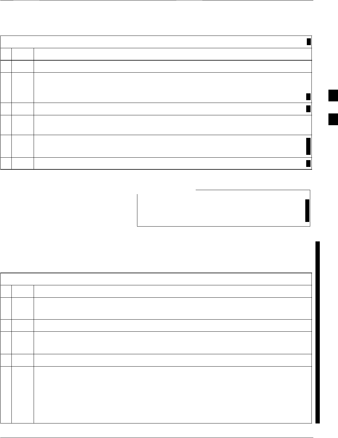
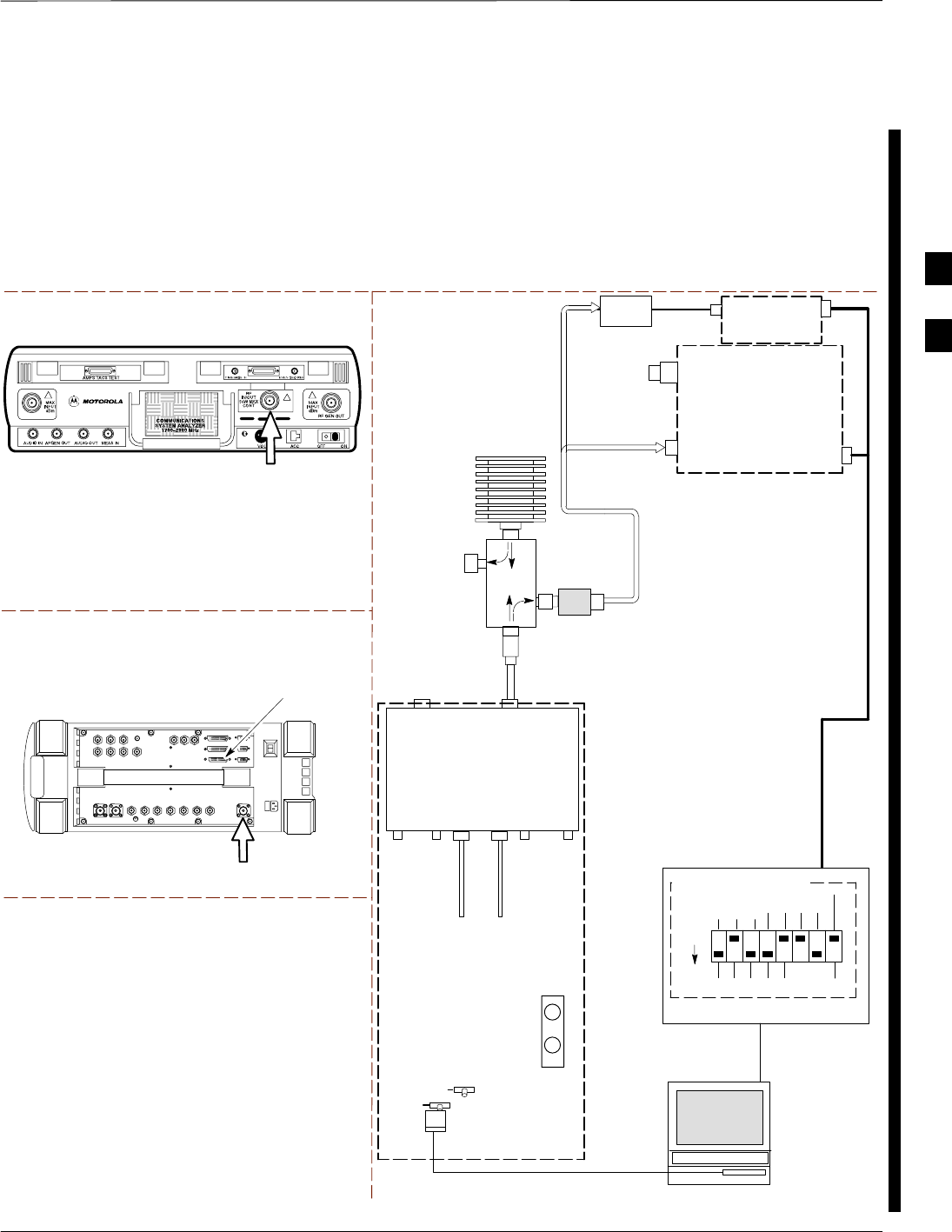
2Remove CSM 2 (if installed) and connect a Serial Cable from the LMF COM 1 Port (via Null Modem
Card) to the MMI Port on CSM 1.
– Refer to Figure 3-11.
3Reinstall CSM 2.
4Start an MMI Communication Session with CSM 1 by using the Windows Desktop Shortcut Icon.
– Refer to Table 3-14 .
5When the Terminal Screen appears press the Enter Key until the CSM> Prompt appears.
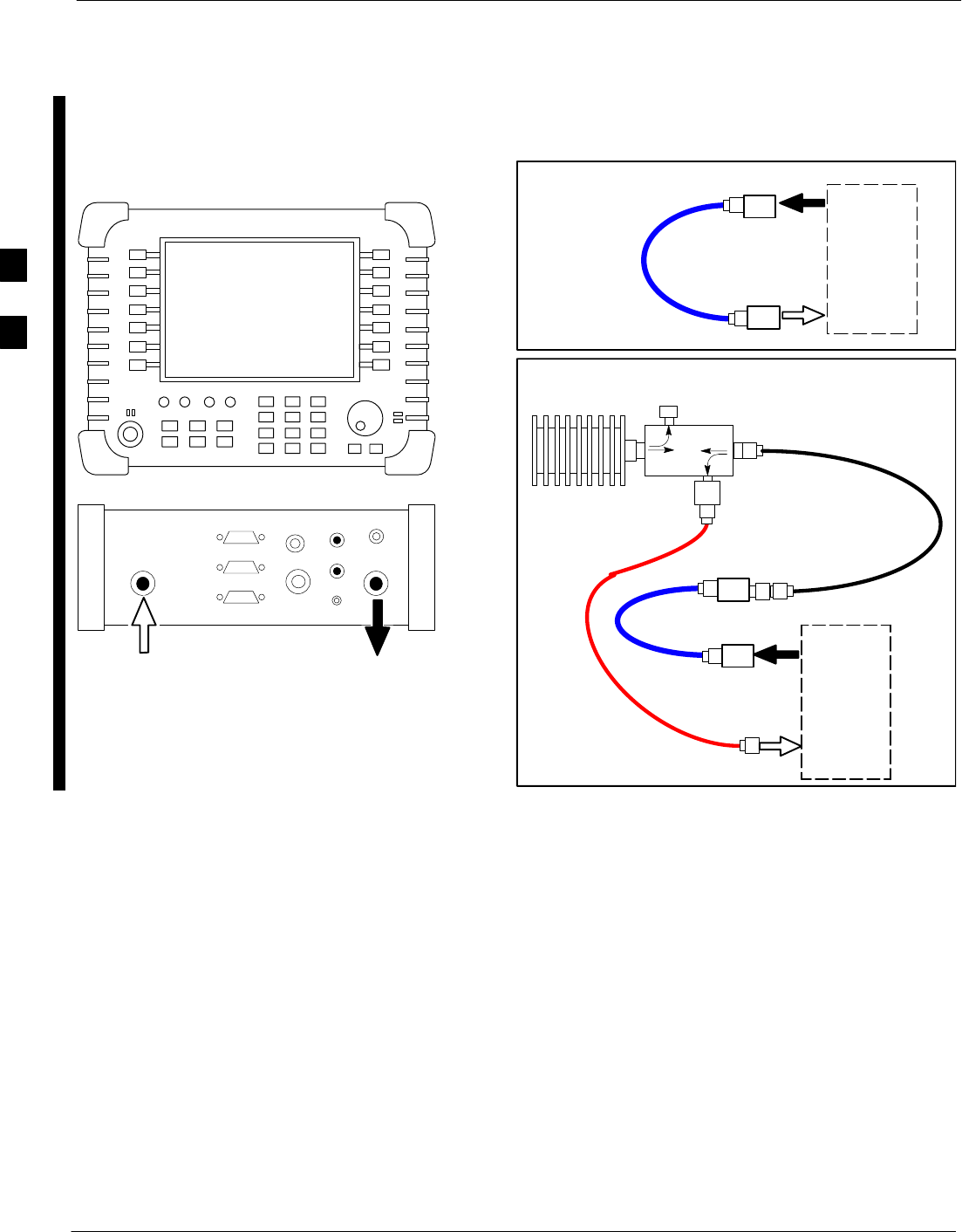
In the Power Entry Compartment, connect the GPS
Antenna to the RF GPS Connector ONLY.
Damage to the GPS Antenna and/or receiver can result if
the GPS Antenna is inadvertently connected to any other
RF Connector.
CAUTION
3
CSM System Time – GPS and HSO Verification – continued
3-52 1X SC 4812T Lite BTS Optimization/ATP FEB 2005
PRELIMINARY
NULL MODEM
BOARD
(TRN9666A)
RS–232 SERIAL
MODEM CABLE
DB9–TO–DB25
ADAPTER
COM1
LMF
NOTEBOOK
FW00372
CSM Card shown
removed from frame
19.6 MHZ TEST
POINT REFERENCE
(NOTE 1)
EVEN SECOND
TICK TEST POINT
REFERENCE
GPS RECEIVER
ANTENNA INPUT
GPS RECEIVER
SERIAL
PORT
ANTENNA COAX
CABLE
REFERENCE
OSCILLATOR
9–PIN TO 9–PIN
RS–232 CABLE
NOTES:
1. One LED on each CSM:
Green = IN–SERVICE ACTIVE
Fast Flashing Green = OOS–RAM
Red = Fault Condition
Flashing Green & Red = Fault
Figure 3-11: CSM MMI Terminal Connection
3

CSM System Time – GPS and HSO Verification – continued
FEB 2005 1X SC 4812T Lite BTS Optimization/ATP 3-53
PRELIMINARY
GPS Initialization/Verification
Prerequisites
Ensure the following prerequisites have been met before proceeding:
– The Primary CSM and HSO (if equipped) has been warmed–up for
at least 15 minutes.
– The LMF Computer is connected to the MMI Port of the Primary
CSM as shown in Figure 3-11.
– An MMI Communication Session has been started (Table 3-14),
and the CSM> Prompt is present in the HyperTerminal Window
(Table 3-23).
Perform the procedure in Table 3-24 to initialize and verify proper GPS
Receiver Functionality.
Table 3-24: GPS Initialization/Verification Procedure
nStep Action
1To verify that the following messages are displayed within the report, issue the following MMI
Command.
Clock alarms (0000), Dpll is locked and has a Reference Source
GPS self test passed
bstatus
– The system will display a response similar to the following:
Clock Alarms (0000):
DPLL is locked and has a Reference Source.
GPS Receiver self test result: passed
Time since reset 0:33:11, time since power on: 0:33:11
2Enter the following command at the CSM> Prompt to display the current status of the Timing
Sources.
sources
– When equipped with HSO, the system will generate a response similar to the following:
Num Source Name Type TO Good Status Last Phase Target Phase Valid
––––––––––––––––––––––––––––––––––––––––––––––––––––––––––––––––––––––––––––
0 Local GPS Primary 4 Yes Good 3 0 Yes
1HSO Backup 4 No N/A timed–out* Timed–out* No
NOTE
Verify that the HSO is FULLY SEATED and LOCKED to prevent any possible card warpage.
“Timed–out” should only be displayed while the HSO is warming up.
“Not–Present” or “Faulty” should not be displayed.
table continued on next page
3

CSM System Time – GPS and HSO Verification – continued
3-54 1X SC 4812T Lite BTS Optimization/ATP FEB 2005
PRELIMINARY
Table 3-24: GPS Initialization/Verification Procedure
nActionStep
3If the HSO does not appear as one of the sources, then configure the HSO as a Back–up Source by
entering the following command at the CSM> Prompt.
csm>ss 1 12
– After a maximum of 15 minutes, the Rubidium Oscillator should reach operational
temperature and the PWR/ALM LED on the HSO should now have changed from red to
green.
SIf the LED is green, proceed to Step 5.
SIf the LED is RED, proceed to Step 4.
4verify that the HSO had been powered–up for at least 5 minutes.
– After the oscillator temperature is stable, the LED should go GREEN.
–Wait for this to occur before continuing!
5After the HSO LED has changed to green, enter the following command at the CSM> Prompt.
csm>sources <cr>
– The HSO should be valid within one (1) minute, assuming the DPLL is locked and the HSO
Rubidium Oscillator is fully warmed.
6Verify that the HSO is now a valid source by confirming that the bold text below matches the
response of the “sources” command.
Num Source Name Type TO Good Status Last Phase Target Phase Valid
––––––––––––––––––––––––––––––––––––––––––––––––––––––––––––––––––––––––––––
0 Local GPS Primary 4 Yes Good 3 0 Yes
1HSO Backup 4 Yes N/A xxxxxxxxxx xxxxxxxxxx Yes
SIf “timed out” is displayed in the Last Phase column, suspect the HSO Output Buffer or
Oscillator to be defective.
– Replace the HSO before proceeding.
SIf “timed out” is not displayed in the “Last Phase” Column, proceed to Step 7.
7HSO Information (underlined text above in Step 6, verified from left to right) is usually the #1
Reference Source.
– If this is not the case, proceed to Step 8.
8At the OMC–R, determine if the correct BTS Timing Source has been identified in the database by
entering the following command.
omc–000000 >display bts csmgen
9From the system response to the command in Step 8, if the correct BTS Timing Source is not
listed, enter the following command to make corrections to the database.
omc–000000 >edit csm csmgen refsrc
table continued on next page
3

CSM System Time – GPS and HSO Verification – continued
FEB 2005 1X SC 4812T Lite BTS Optimization/ATP 3-55
PRELIMINARY
Table 3-24: GPS Initialization/Verification Procedure
nActionStep
10 Verify that the following GPS information (underlined text in Step 6) is true.
– The GPS is usually the “0” Reference Source.
– At least one Primary Reference Source must indicate “Status = good” and “Valid = yes” to
bring the site up.
11 Enter the following command at the CSM> Prompt to verify that the GPS Receiver is in Tracking
Mode.
csm>gstatus
Observe the following typical system response.
24:06:08 GPS Receiver Control Task State: tracking satellites.
24:06:08 Time since last valid fix: 0 seconds.
24:06:08
24:06:08 Recent Change Data:
24:06:08 Antenna cable delay 0 ns.
24:06:08 Initial position: lat 117650000 msec, lon –350258000 msec, height 0 cm (GPS)
24:06:08 Initial Position Accuracy (0): estimated.
24:06:08
24:06:08 GPS Receiver Status:
24:06:08 Position hold: lat 118245548 msec, lon –350249750 msec, height 20270 cm
24:06:08 Current position: lat 118245548 msec, lon –350249750 msec, height 20270 cm
(GPS)
24:06:08 8 satellites tracked, receiving 8 satellites, 8 satellites visible.
24:06:08 Current Dilution of Precision (PDOP or HDOP): 0.
24:06:08 Date & Time: 1998:01:13:21:36:11
24:06:08 GPS Receiver Status Byte: 0x08
24:06:08 Chan:0, SVID: 16, Mode: 8, RSSI: 148, Status: 0xa8
24:06:08 Chan:1, SVID: 29, Mode: 8, RSSI: 132, Status: 0xa8
24:06:08 Chan:2, SVID: 18, Mode: 8, RSSI: 121, Status: 0xa8
24:06:08 Chan:3, SVID: 14, Mode: 8, RSSI: 110, Status: 0xa8
24:06:08 Chan:4, SVID: 25, Mode: 8, RSSI: 83, Status: 0xa8
24:06:08 Chan:5, SVID: 3, Mode: 8, RSSI: 49, Status: 0xa8
24:06:08 Chan:6, SVID: 19, Mode: 8, RSSI: 115, Status: 0xa8
24:06:08 Chan:7, SVID: 22, Mode: 8, RSSI: 122, Status: 0xa8
24:06:08
24:06:08 GPS Receiver Identification:
24:06:08 COPYRIGHT 1991–1996 MOTOROLA INC.
24:06:08 SFTW P/N # 98–P36830P
24:06:08 SOFTWARE VER # 8
24:06:08 SOFTWARE REV # 8
24:06:08 SOFTWARE DATE 6 AUG 1996
24:06:08 MODEL # B3121P1115
24:06:08 HDWR P/N # _
24:06:08 SERIAL # SSG0217769
24:06:08 MANUFACTUR DATE 6B07
24:06:08 OPTIONS LIST IB
24:06:08 The receiver has 8 channels and is equipped with TRAIM.
12 Verify the following GPS information (shown in Step 11 above in underlined text):
– At least four satellites are being tracked, and four satellites are visible.
– GPS Receiver Control Task State is “tracking satellites”. Do not continue until this occurs!
– Dilution of Precision Indication is not more that 30.
table continued on next page
3

CSM System Time – GPS and HSO Verification – continued
3-56 1X SC 4812T Lite BTS Optimization/ATP FEB 2005
PRELIMINARY
Table 3-24: GPS Initialization/Verification Procedure
nActionStep
13 Record the current position Base Site Latitude, Longitude, Height and Height Reference (Height
Reference to Mean Sea Level (MSL) or GPS Height (GPS): GPS = 0 MSL = 1.
14 If Steps 1 through 12 pass, the GPS is good.
NOTE
If any of the above mentioned areas fail, verify that:
SIf Initial Position Accuracy is “estimated” (typical), at least four satellites must be tracked and
visible (one satellite must be tracked and visible if actual Latitude, Longitude, and Height Data
for this site has been entered into CDF File).
SIf Initial Position Accuracy is “surveyed,” Position Data currently in the CDF File is assumed
to be accurate.
– The GPS will not automatically survey and update its position.
SThe GPS Antenna is not obstructed or misaligned.
SThe GPS Antenna Connector Center Conductor measures approximately +5V DC with respect
to the Shield.
SThere is no more than 4.5 dB of Signal Loss between the GPS Antenna OSX Connector and the
BTS Frame GPS Input.
SAny Lightning Protection installed between the GPS Antenna and the BTS Frame is installed
correctly.
15 Enter the following command at the CSM> Prompt to verify that the CSM is warmed–up and that
GPS Acquisition has taken place.
csm>debug dpllp
SIf the CSM is warmed–up, proceed to Step 17.
SIf the CSM is not warmed–up (15 minutes from application of power), proceed to Step 16.
16 Observe the following typical response if the CSM is not warmed–up.
CSM>DPLL Task Wait. 884 seconds left.
DPLL Task Wait. 882 seconds left.
DPLL Task Wait. 880 seconds left. ...........etc.
NOTE
The warm command can be issued at the MMI Port used to force the CSM into Warm–up Mode,
but the Reference Oscillator will be unstable.
17 Observe the following typical response if the CSM is warmed–up.
c:17486 off: –11, 3, 6 TK SRC:0 S0: 3 S1:–2013175,–2013175
c:17486 off: –11, 3, 6 TK SRC:0 S0: 3 S1:–2013175,–2013175
c:17470 off: –11, 1, 6 TK SRC:0 S0: 1 S1:–2013175,–2013175
c:17486 off: –11, 3, 6 TK SRC:0 S0: 3 S1:–2013175,–2013175
c:17470 off: –11, 1, 6 TK SRC:0 S0: 1 S1:–2013175,–2013175
c:17470 off: –11, 1, 6 TK SRC:0 S0: 1 S1:–2013175,–2013175
table continued on next page
3
CSM System Time – GPS and HSO Verification – continued
FEB 2005 1X SC 4812T Lite BTS Optimization/ATP 3-57
PRELIMINARY
Table 3-24: GPS Initialization/Verification Procedure
nActionStep
18 Verify the following GPS information (underlined text in Step 17, from left to right):
– Lower Limit Offset from Tracked Source Variable is not less than –60 (equates to 3µs Limit).
– Upper Limit Offset from Tracked Source Variable is not more than +60 (equates to 3µs
Limit).
– TK SRC: 0 is selected, where SRC 0 = GPS.
19 Enter the following commands at the CSM> Prompt to exit the Debug Mode Display.
csm>debug dpllp
3

CSM System Time – GPS and HSO Verification – continued
3-58 1X SC 4812T Lite BTS Optimization/ATP FEB 2005
PRELIMINARY
Connecting Test Equipment to
the BTS
The following types of Test Equipment are required to perform
Calibration and ATP Tests:
SLMF
SCommunications System Analyzer Model supported by the LMF
SPower Meter Model supported by the LMF (required when using the
HP 8921A/600 and Advantest R3465 Analyzers)
SNon–radiating Transmit Line Termination Load
SDirectional Coupler and In–line Attenuator
SRF Cables and Adapters
Refer to Table 3-25 for an overview of Test Equipment Connections for
currently supported by the LMF. In addition, see the following figures:
SFigure 3-16, Figure 3-17, and Figure 3-18 show the Test Set
Connections for TX Calibration
SFigure 3-20 through Figure 3-25 show the Test Set Connections for
Optimization/ATP Tests
Test Equipment GPIB Address
Settings
All Test Equipment is controlled by the LMF through an
IEEE–488/GPIB Bus. To communicate on the Bus, each piece of Test
Equipment must have a GPIB Address Set that the LMF will recognize.
The Standard Address Settings used by the LMF for the various types of
Test Equipment Items are as follows:
SSignal Generator Address: 1
SPower Meter Address: 13
SCommunications System Analyzer Address: 18
Using the procedures included in the Verifying and Setting GPIB
Addresses section of Appendix F, verify and, if necessary, change the
GPIB Address of each piece of employed Test Equipment to match the
applicable addresses above.
Supported Test Equipment
To prevent damage to the Test Equipment, all Transmit
(TX) Test Connections must be through a 30 dB
Directional Coupler plus a 20dB In-line Attenuator for
both the 800 MHz and 1.9 GHz BTSs.
CAUTION
3

CSM System Time – GPS and HSO Verification – continued
FEB 2005 1X SC 4812T Lite BTS Optimization/ATP 3-59
PRELIMINARY
IS–95A/B Operation
Optimization and ATP Testing for IS–95A/B Sites and Carriers may be
performed using the following Test Equipment:
SCyberTest
SAdvantest R3267 Spectrum Analyzer with R3562 Signal Generator
SAdvantest R3465 Spectrum Analyzer with R3561L Signal Generator
and HP–437B or Gigatronics Power Meter
SAgilent E4406A Transmitter Test Set with E4432B Signal Generator
SAgilent 8935 Series E6380A Communications Test Set (formerly HP
8935)
SHewlett–Packard HP 8921 (with CDMA Interface and, for 1.9 GHz,
PCS Interface) and HP–437B or Gigatronics Power Meter
SSpectrum Analyzer (HP8594E) – optional
SRubidium Standard Timebase – optional
CDMA2000 1X Operation
Optimization and ATP Testing for CDMA2000 1X Sites and Carriers
may be performed using the following Test Equipment:
SAdvantest R3267 Spectrum Analyzer with R3562 Signal Generator
SAgilent E4406A Transmitter Test Set with E4432B Signal Generator
SAgilent 8935 Series E6380A Communications Test Set (formerly HP
8935) with Option 200 or R2K and with E4432B Signal Generator for
1X FER
SAgilent E7495A Communications Test Set
Test Equipment Preparation
See Appendix F for specific steps to prepare each type of Test Set and
Power Meter to perform Calibration and ATP.
Agilent E7495A Communications Test Set requires additional set–up
and preparation. This is described in detail in Appendix F.
Test Equipment Connection
Charts
To use the following charts to identify necessary Test Equipment
Connections, locate the Communications System Analyzer being used in
the COMMUNICATIONS SYSTEM ANALYZER Columns, and read
down the column. Where a dot appears in the column, connect one end
of the Test Cable to that Connector. Follow the horizontal line to locate
the end connection(s), reading up the column to identify the appropriate
Test Equipment and/or BTS Connector.
3

CSM System Time – GPS and HSO Verification – continued
3-60 1X SC 4812T Lite BTS Optimization/ATP FEB 2005
PRELIMINARY
IS–95A/B–only Test Equipment Connections
Table 3-25 depicts the Interconnection Requirements for currently
available Test Equipment supporting IS–95A/B only that meets Motorola
Standards and is supported by the LMF.
Table 3-25: IS–95A/B–only Test Equipment Interconnection
COMMUNICATIONS SYSTEM ANALYZER ADDITIONAL TEST EQUIPMENT
SIGNAL Cyber–Test Advantest
R3465 HP 8921A HP 8921
W/PCS Power
Meter GPIB
Interface LMF
Attenuator
and
Directional
Coupler BTS
EVEN SECOND
SYNCHRONIZATION EVEN
SEC REF EVEN SEC
SYNC IN
EVEN
SECOND
SYNC IN
EVEN
SECOND
SYNC IN
19.6608 MHZ
CLOCK TIME
BASE IN
CDMA
TIME BASE
IN
CDMA
TIME BASE
IN
CDMA
TIME BASE
IN
CONTROL
IEEE 488 BUS IEEE
488 GPIB GPIB SERIAL
PORT
HP–I
BHP–IB
TX TEST
CABLES RF
IN/OUT INPUT
50WTX1–6
RF
IN/OUT RF
IN/OUT 20 DB
ATTEN. BTS
PORT
RX TEST
CABLES RF
GEN OUT RF OUT
50WRX1–6
DUPLEX
OUT RF OUT
ONLY
SYNC
MON-
ITOR
FREQ
MON-
ITOR
HP–IB
3
CSM System Time – GPS and HSO Verification – continued
FEB 2005 1X SC 4812T Lite BTS Optimization/ATP 3-61
PRELIMINARY
CDMA2000 1X/IS–95A/B–capable Test Equipment
Connections
Table 3-26 depicts the Interconnection Requirements for currently
available Test Equipment supporting both CDMA 2000 1X and
IS–95A/B that meets Motorola Standards and is supported by the LMF.
Table 3-26: CDMA2000 1X/IS–95A/B Test Equipment Interconnection
COMMUNICATIONS SYSTEM ANALYZER ADDITIONAL TEST EQUIPMENT
SIGNAL
Agilent
8935
(Option 200
or R2K) Agilent
E7495A
Advan
test
R3267 Agilent
E4406A Signal
Generator
Advant-
est
R3562
Signal
Genera-
tor Power
Meter
GPIB
Inter-
face LMF
30 dB
Directional
Coupler and
20dB Pad* BTS
EVEN SECOND
SYNCHRONIZATION EXT
TRIG IN EXT
TRIG TRIGGER
IN
19.6608 MHZ
CLOCK MOD TIME
BASE IN EXT REF
IN
CONTROL
IEEE 488 BUS IEEE
488 GPIB HP–IB GPIB SERIAL
PORT
HP–IB
TX TEST
CABLES RF
IN/OUT RF IN TX1–6
RF INPUT
50 OHM 30 DB COUPLER
AND 20 DB PAD
RX TEST
CABLES RF OUT
50 OHM
RF OUT 50
OHM RX1–6
RF OUT
ONLY
SYNC
MONI
TOR
FREQ
MONITOR
PATTERN
TRIG IN
GPIB
RF OUTPUT
50 OHM
RF OUTPUT
50 OHM
10 MHZ IN 10 MHZ OUT
(SWITCHED) 10 MHZ IN
10 MHZ
OUT
10 MHZ
SERIAL
I/O SERIAL
I/O
SIGNAL SOURCE
CONTROLLED
SERIAL I/O
EVEN
SECOND
SYNC IN
EXT REF
IN
HP–IB
RF IN/OUT
DUPLEX
OUT *
SYNTHE
REF IN
* WHEN USED ALONE, THE AGILENT 8935 WITH OPTION 200 OR R2K SUPPORTS IS–95A/B RX TESTING BUT NOT CDMA2000 1X RX TESTING.
EVEN
SECOND
SYNC IN
PORT 1
RF OUT
PORT 2
RF IN
3
CSM System Time – GPS and HSO Verification – continued
3-62 1X SC 4812T Lite BTS Optimization/ATP FEB 2005
PRELIMINARY
Equipment Warm-up
To assure BTS stability and contribute to Optimization
accuracy of the BTS, warm-up the BTS Test Equipment
prior to performing the BTS Optimization Procedure as
follows:
– Agilent E7495A for a minimum of 30 minutes
– All other Test Sets for a minimum of 60 minutes
Time spent running initial or normal Power-up, Hardware/
Firmware Audit, and BTS Download counts as Warm-up
Time.
NOTE
Before installing any Test Equipment directly to any BTS
TX OUT Connector, verify that there are no CDMA
Channels keyed.
– At active sites, have the OMC-R/CBSC place the
antenna (sector) assigned to the BBX under test to out
of service (OOS). Failure to do so can result in
serious personal injury and/or equipment damage.
WARNING
Automatic Cable Calibration
Set–up
Figure 3-12 and Figure 3-13 show the Cable Calibration Set–up for the
Test Sets supported by the LMF. The left side of the diagram depicts the
location of the Input and Output Connectors of each Test Equipment
Item, and the right side details the connections for each test. Table 3-32
provides a procedure for performing Automatic Cable Calibration.
Manual Cable Calibration
If Manual Cable Calibration is required, refer to the procedures in
Appendix F.
3
CSM System Time – GPS and HSO Verification – continued
FEB 2005 1X SC 4812T Lite BTS Optimization/ATP 3-63
PRELIMINARY
Motorola CyberTest
Advantest Model R3465
RF OUT 50Ω
INPUT 50Ω
RF GEN OUTANT IN
SUPPORTED TEST SETS
100–WATT (MIN)
NON–RADIATING
RF LOAD
TEST
SET
A. SHORT CABLE CAL
SHORT
CABLE
B. RX TEST CAL SET–UP FOR TRF
TEST
SET
C. TX TEST AND DRF RX TEST CAL SET–UP
20DB IN–LINE
ATTENUATOR
CALIBRATION SET–UP
N–N FEMALE
ADAPTER
TX
CABLE
SHORT
CABLE
Note: The 30 dB Directional Coupler is not used
with the Cybertest Test Set. The TX cable is
connected directly to the Cybertest Test Set.
A 10dB Attenuator must be used with the Short
Test Cable for Cable Calibration with the CyberTest
Test Set. The 10dB Attenuator is used only for the
Cable Calibration Procedure, not with the Test
Cables for TX Calibration and ATP Tests.
TEST
SET
RX
CABLE
SHORT
CABLE
DIRECTIONAL
COUPLER
(30 DB)
N–N FEMALE
ADAPTER
50 Ω
ΤERM.
Agilent 8935 Series E6380A
(formerly HP 8935)
RF
IN/OUT
ANT
IN
Hewlett Packard Model HP 8921A
Note: For 800 MHZ only. The HP 8921A cannot
be used to calibrate cables for PCS frequencies.
TX CABLE FOR
TX TEST CABLE
CALIBRATION
RX CABLE FOR DRF
RX TEST
CABLE CALIBRATION
DUPLEX
OUT ANT
IN
Figure 3-12: IS–95A/B Cable Calibration Test Set–up – CyberTest, Agilent 8935, Advantest R3465,
and HP 8921A
3
CSM System Time – GPS and HSO Verification – continued
3-64 1X SC 4812T Lite BTS Optimization/ATP FEB 2005
PRELIMINARY
TEST
SET
A. SHORT CABLE CAL
SHORT
CABLE
B. RX TEST SET–UP FOR TRF
CALIBRATION SET–UP
TEST
SET
RX
CABLE
SHORT
CABLE
N–N FEMALE
ADAPTER
SUPPORTED TEST SETS
INPUT 50 Ω
RF OUT
50 Ω
Advantest R3267 (Top) and R3562 (Bottom)
NOTE:
SYNTHE REF IN ON REAR OF SIGNAL GENERATOR IS
CONNECTED TO 10 MHZ OUT ON REAR OF SPECTRUM
ANALYZER
Agilent E4432B (Top) and E4406A (Bottom)
NOTE:
10 MHZ IN ON REAR OF SIGNAL GENERATOR IS CONNECTED TO
10 MHZ OUT (SWITCHED) ON REAR OF TRANSMITTER TESTER
(FIGURE F-18).
RF INPUT
50 Ω
RF OUTPUT
50 Ω
100–WATT (MIN)
NON–RADIATING
RF LOAD
TEST
SET
D. TX TEST SET–UP AND DRF RX TEST
SET–UP
20DB IN–LINE
ATTENUATOR
N–N FEMALE
ADAPTER
TX
CABLE
SHORT
CABLE
DIRECTIONAL
COUPLER
(30 DB)
50 Ω
ΤERM.
TX CABLE FOR
TX TEST CABLE
CALIBRATION
RX CABLE FOR DRF
RX TEST
CABLE CALIBRATION
Figure 3-13: IS–95A/B and CDMA 2000 1X Cable Calibration Test Set–up –
Agilent E4406A/E4432B and Advantest R3267/R3562
3
CSM System Time – GPS and HSO Verification – continued
FEB 2005 1X SC 4812T Lite BTS Optimization/ATP 3-65
PRELIMINARY
TEST
SET
A. SHORT CABLE CAL
SHORT
CABLE
B. RX TEST SET–UP FOR TRF
CALIBRATION SET–UP
TEST
SET
RX
CABLE
SHORT
CABLE
N–N FEMALE
ADAPTER
SUPPORTED TEST SETS
Agilent E4432B (Top) and 8935 Series
E6380A (Bottom)
NOTE:
10 MHZ IN ON REAR OF SIGNAL GENERATOR IS CONNECTED TO
10 MHZ REF OUT ON SIDE OF CDMA BASE STATION TEST SET
(FIGURE F-17).
RF OUTPUT
50 Ω
100–WATT (MIN)
NON–RADIATING
RF LOAD
TEST
SET
D. TX TEST SET–UP AND DRF RX TEST
SET–UP
20DB IN–LINE
ATTENUATOR
N–N FEMALE
ADAPTER
TX
CABLE
SHORT
CABLE
DIRECTIONAL
COUPLER
(30 DB)
50 Ω
ΤERM.
TX CABLE FOR
TX TEST CABLE
CALIBRATION
RX CABLE FOR DRF
RX TEST
CABLE CALIBRATION
ANT
IN
Figure 3-14: CDMA2000 1X Cable Calibration Test Set–up – Agilent 8935/E4432B
3
CSM System Time – GPS and HSO Verification – continued
3-66 1X SC 4812T Lite BTS Optimization/ATP FEB 2005
PRELIMINARY
TEST
SET
A. SHORT CABLE CAL
SHORT
CABLE
CALIBRATION SET–UP
100–WATT (MIN)
NON–RADIATING
RF LOAD
D. RX and TX TEST SET–UP
20DB IN–LINE
ATTENUATOR
N–N FEMALE
ADAPTER
TX
CABLE
DIRECTIONAL
COUPLER
(30 DB)
50 Ω
ΤERM.
TX CABLE FOR
TX TEST CABLE
CALIBRATION
RX CABLE FOR DRF
RX TEST
CABLE CALIBRATION
10 DB PAD
10 DB PAD
SHORT
CABLE
10 DB PAD
10 DB PAD
TEST
SET
SUPPORTED TEST SETS
Agilent E7495A
PORT 1
RF OUT
PORT 2
RF IN
Use only
Agilent supplied
power adapter
GPS
GPIO
Serial 1
Serial 2
Power REF
50 MHz
Sensor
Ext Ref
In
Even Second
Sync In
Antenna
Port 1
RF Out / SWR
Port 2
RF In
Figure 3-15: CDMA2000 1X Cable Calibration Test Set–up – Agilent E7495A
3
CSM System Time – GPS and HSO Verification – continued
FEB 2005 1X SC 4812T Lite BTS Optimization/ATP 3-67
PRELIMINARY
Set-up for TX Calibration
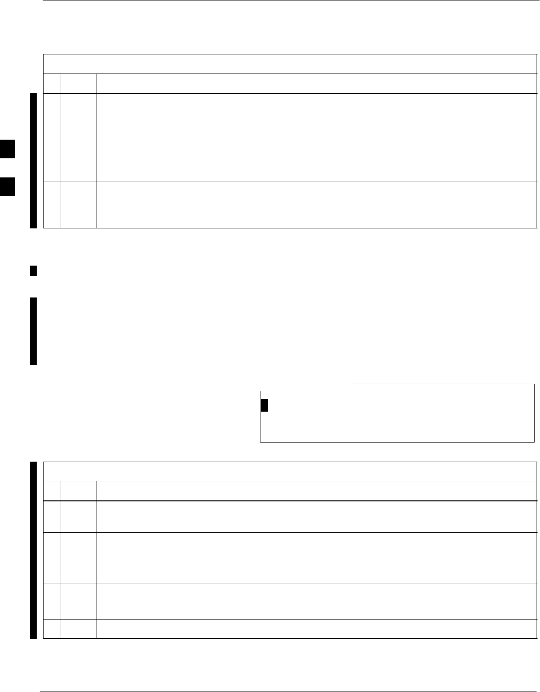
Figure 3-16 and Figure 3-17 show the Test Set Connections for TX
Calibration.
Motorola CyberTest
Agilent 8935 Series E6380A (formerly HP 8935)
TEST SETS TRANSMIT (TX) SET–UP
FRONT PANEL
RF
IN/OUT
RF
IN/OUT
HP–IB
TO GPIB
BOX
NOTE: THE 30 DB DIRECTIONAL COUPLER IS NOT USED WITH THE
CYBERTEST TEST SET. THE TX CABLE IS CONNECTED DIRECTLY
TO THE CYBERTEST TEST SET.
TO
MPC
TO PA
TRUNKING
MODULE
RS232–GPIB
INTERFACE BOX
INTERNAL PCMCIA
ETHERNET CARD
GPIB
CABLE
UNIVERSAL TWISTED PAIR (UTP)
CABLE (RJ45 CONNECTORS)
RS232 NULL
MODEM
CABLE
S MODE
DATA FORMAT
BAUD RATE
GPIB ADRS G MODE
ON
BTS
INTERNAL
TX
CABLE
CDMA
LMF
DIP SWITCH SETTINGS
10BASET/
10BASE2
CONVERTER
LAN
B
LAN
A
GPIB
RF IN/OUT
RX
ANTENNA
CONNECTOR
FREQ
MONITOR
SYNC
MONITOR
CSM
INTERNAL
RX
CABLE
TX
ANT
CPLD
RX
BTS
CPLD
TRF
TX
BTS
CPLD
RX
ANT
CPLD
TX
ANTENNA
CONNECTOR
COMMUNI–
CATIONS
System
Analyzer
2O DB IN–LINE
ATTENUATOR
50 Ω
TERM
.
TX TEST
CABLE
DIRECTIONAL
COUPLER
(30 DB)
100–WATT (MIN.)
NON–RADIATING
RF LOAD
TX TEST
CABLE
* BLACK RECTANGLES
REPRESENT THE RAISED
PART OF SWITCHES
NOTE: IF BTS IS EQUIPPED
WITH DRFS (DUPLEXED
RX/TX SIGNALS), CONNECT
THE TX TEST CABLE TO
THE DRF ANTENNA
CONNECTOR.
POWER
METER
(OPTIONAL)*
POWER
SENSOR
* A POWER METER CAN BE USED IN
PLACE OF THE COMMUNICATIONS
TEST SET FOR TX CALIBRATION/
AUDIT
Figure 3-16: TX Calibration Test Set–up –
CyberTest (IS–95A/B) and Agilent 8935 (IS–95A/B and CDMA2000 1X)
3

CSM System Time – GPS and HSO Verification – continued
3-68 1X SC 4812T Lite BTS Optimization/ATP FEB 2005
PRELIMINARY
TEST SETS TRANSMIT (TX) SET–UP
NOTE: THE HP 8921A AND ADVANTEST
R3465 CANNOT BE USED FOR TX
CALIBRATION. A POWER METER MUST BE
USED.
TO
MPC
TO PA
TRUNKING
MODULE
RS232–GPIB
INTERFACE BOX
INTERNAL PCMCIA
ETHERNET CARD
GPIB
CABLE
UNIVERSAL TWISTED PAIR (UTP)
CABLE (RJ45 CONNECTORS)
RS232 NULL
MODEM
CABLE
S MODE
DATA FORMAT
BAUD RATE
GPIB ADRS G MODE
ON
BTS
INTERNAL
TX
CABLE
CDMA
LMF
DIP SWITCH SETTINGS
10BASET/
10BASE2
CONVERTER
LAN
B
LAN
A
RX
ANTENNA
CONNECTOR
FREQ
MONITOR
SYNC
MONITOR
CSM
INTERNAL
RX
CABLE
TX
ANT
CPLD
RX
BTS
CPLD
TRF
TX
BTS
CPLD
RX
ANT
CPLD
TX
ANTENNA
CONNECTOR
50 Ω
TERM
.
TX TEST
CABLE
DIRECTIONAL
COUPLER
(30 DB)
100–WATT (MIN.)
NON–RADIATING
RF LOAD
TX TEST
CABLE
* BLACK RECTANGLES
REPRESENT THE RAISED
PART OF SWITCHES
NOTE: IF BTS IS EQUIPPED
WITH DRFS (DUPLEXED
RX/TX SIGNALS), CONNECT
THE TX TEST CABLE TO
THE DRF ANTENNA
CONNECTOR.
POWER
SENSOR POWER METER
2O DB IN–LINE
ATTENUATOR
Figure 3-17: TX Calibration Test Set–up – Using Power Meter
3
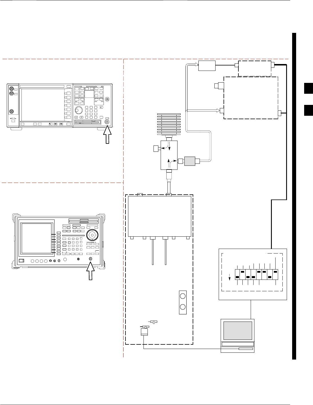
CSM System Time – GPS and HSO Verification – continued
FEB 2005 1X SC 4812T Lite BTS Optimization/ATP 3-69
PRELIMINARY
TEST SETS TRANSMIT (TX) SET–UP
TO
MPC
TO PA
TRUNKING
MODULE
RS232–GPIB
INTERFACE BOX
INTERNAL PCMCIA
ETHERNET CARD
GPIB
CABLE
UNIVERSAL TWISTED PAIR (UTP)
CABLE (RJ45 CONNECTORS)
RS232 NULL
MODEM
CABLE
S MODE
DATA FORMAT
BAUD RATE
GPIB ADRS G MODE
ON
BTS
INTERNAL
TX
CABLE
CDMA
LMF
DIP SWITCH SETTINGS
10BASET/
10BASE2
CONVERTER
LAN
B
LAN
A
GPIB
RF INPUT 50 Ω
OR INPUT 50 Ω
RX
ANTENNA
CONNECTOR
FREQ
MONITOR
SYNC
MONITOR
CSM
INTERNAL
RX
CABLE
TX
ANT
CPLD
RX
BTS
CPLD
TRF
TX
BTS
CPLD
RX
ANT
CPLD
TX
ANTENNA
CONNECTOR
COMMUNI–
CATIONS
System
Analyzer
50 Ω
TERM
.
TX TEST
CABLE
DIRECTIONAL
COUPLER
(30 DB)
100–WATT (MIN.)
NON–RADIATING
RF LOAD
TX TEST
CABLE
* BLACK RECTANGLES
REPRESENT THE RAISED
PART OF SWITCHES
NOTE: IF BTS IS EQUIPPED
WITH DRFS (DUPLEXED
RX/TX SIGNALS), CONNECT
THE TX TEST CABLE TO
THE DRF ANTENNA
CONNECTOR.
POWER
METER
(OPTIONAL)*
POWER
SENSOR
* A POWER METER CAN BE USED IN
PLACE OF THE COMMUNICATIONS
TEST SET FOR TX CALIBRATION/
AUDIT
RF INPUT
50 Ω
Agilent E4406A
INPUT 50 Ω
Advantest R3267
2O DB IN–LINE
ATTENUATOR
Figure 3-18: TX Calibration Test Set–up –
Agilent E4406A and Advantest R3567 (IS–95A/B and CDMA2000 1X)
3

CSM System Time – GPS and HSO Verification – continued
3-70 1X SC 4812T Lite BTS Optimization/ATP FEB 2005
PRELIMINARY
TEST SETS TRANSMIT (TX) SET–UP
INTERNAL PCMCIA
ETHERNET CARD
BTS
CDMA
LMF
10BASET/
10BASE2
CONVERTER
LAN
B
LAN
A
RX
ANTENNA
CONNECTOR
SYNC
MONITOR
CSM
TX
ANTENNA
CONNECTOR
50 Ω
TERM
.
TX TEST
CABLE
DIRECTIONAL
COUPLER
(30 DB)
100–WATT (MIN.)
NON–RADIATING
RF LOAD
TX TEST
CABLE
NOTE: IF BTS IS EQUIPPED
WITH DUPLEXED RX/TX
SIGNALS, CONNECT THE TX
TEST CABLE TO THE
DUPLEXED ANTENNA
CONNECTOR.
POWER
SENSOR
2O DB IN–LINE
ATTENUATOR
ETHERNET HUB
UNIVERSAL TWISTED PAIR (UTP)
CABLE (RJ45 CONNECTORS)
Agilent E7495A
PORT 1
RF OUT
PORT 2
RF IN
SYNC MONITOR
EVEN SEC TICK
PULSE REFERENCE
FROM CSM BOARD
Use only
Agilent supplied
power adapter
GPS
GPIO
Serial 1
Serial 2
Power REF
50 MHz
Sensor
Ext Ref
In
Even Second
Sync In
Antenna
Port 1
RF Out / SWR
Port 2
RF In
INTERNAL
ETHERNET
CARD
COMMUNICATIONS
System Analyzer
POWER METER
PORT 2
RF IN
PORT 1
RF OUT
POWER
SENSOR
Figure 3-19: TX Calibration Test Set–up – Agilent E7495A (IS–95A/B and CDMA2000 1X)
3

CSM System Time – GPS and HSO Verification – continued
FEB 2005 1X SC 4812T Lite BTS Optimization/ATP 3-71
PRELIMINARY
Set–up for ATP Figure 3-20 and Figure 3-21 show the Test Set Connections for ATP Tests.
Motorola CyberTest
TEST SETS Optimization/ATP SET–UP
RF
IN/OUT
SYNC MONITOR
EVEN SEC TICK
PULSE REFERENCE
FROM CSM BOARD
FREQ MONITOR
19.6608 MHZ CLOCK
REFERENCE FROM
CSM BOARD
Advantest Model R3465
INPUT 50Ω
GPIB CONNECTS
TO BACK OF UNIT
NOTE:
The 30 dB Directional Coupler is not used with the
Cybertest Test Set. The TX cable is connected directly to
the Cybertest Test Set.
RF OUT 50Ω
FREQ MONITOR
19.6608 MHZ CLOCK
REFERENCE FROM
CSM BOARD
RF GEN
OUT
SYNC MONITOR EVEN
SEC TICK PULSE
REFERENCE FROM
CSM BOARD
BNC
“T”
TO EXT TRIGGER CONNECTOR
ON REAR OF TEST SET
(FOR DETAILS, SEE
FIGURE F-15)
TO
MPC
TO PA
TRUNKING
MODULE
RS232–GPIB
INTERFACE BOX
INTERNAL PCMCIA
ETHERNET CARD
GPIB
CABLE
UNIVERSAL TWISTED PAIR (UTP)
CABLE (RJ45 CONNECTORS)
RS232 NULL
MODEM
CABLE
S MODE
DATA FORMAT
BAUD RATE
GPIB ADRS G MODE
ON
BTS
INTERNAL
TX
CABLE
CDMA
LMF
DIP SWITCH SETTINGS
10BASET/
10BASE2
CONVERTER
LAN
B
LAN
A
RX TEST
CABLE
GPIB
RF IN/OUT
OR
INPUT 50 Ω
RF GEN OUT,
RF OUT 50Ω,
OR RF IN/OUT
RX
ANTENNA
CONNECTOR
FREQ
MONITOR
SYNC
MONITOR
CSM
INTERNAL
RX
CABLE
TX
ANT
CPLD
RX
BTS
CPLD
TRF
TX
BTS
CPLD
RX
ANT
CPLD
TX
ANTENNA
CONNECTOR
COMMUNICATIONS
System Analyzer
50 Ω
TERM
.
TX TEST
CABLE
DIRECTIONAL
COUPLER
(30 DB)
100–WATT (MIN.)
NON–RADIATING
RF LOAD
TX TEST
CABLE
* BLACK RECTANGLES
REPRESENT THE RAISED
PART OF SWITCHES
CDMA
TIMEBASE
IN
EVEN
SECOND/
SYNC IN
NOTE: IF BTS IS EQUIPPED
WITH DRFS (DUPLEXED RX/TX
SIGNALS), BOTH THE TX AND RX
TEST CABLES CONNECT TO THE
DRF ANTENNA CONNECTOR..
REFER TO FIGURE 3-22.)
2O DB IN–LINE
ATTENUATOR
IMPORTANT:
WHEN PERFORMING FER TEST ON COMPANION FRAME DIVERSITY RX, CONNECT
RX TEST CABLE TO RX ANTENNA PORT ON COLLOCATED COMPANION FRAME.
Agilent 8935 Series E6380A (formerly HP 8935)
RF IN/OUT
HP–IB
TO GPIB
BOX
SYNC MONITOR
EVEN SEC TICK
PULSE REFERENCE
FROM CSM BOARD
FREQ MONITOR
19.6608 MHZ CLOCK
REFERENCE FROM
CSM BOARD
10 MHZ
REF OUT
Figure 3-20: IS–95A/B ATP Test Set–up, TRF Shown – CyberTest, Advantest R3465, and Agilent 8935
3

CSM System Time – GPS and HSO Verification – continued
3-72 1X SC 4812T Lite BTS Optimization/ATP FEB 2005
PRELIMINARY
RF OUT
ONLY
Hewlett Packard Model HP 8921A W/PCS Interface
(for 1900 MHz)
GPIB
CONNECTS
TO BACK OF
UNITS
SYNC MONITOR
EVEN SEC TICK
PULSE REFERENCE
FROM CSM BOARD
FREQ MONITOR
19.6608 MHZ CLOCK
REFERENCE FROM
CSM BOARD
TEST SETS Optimization/ATP SET–UP
RF
IN/OUT
GPIB
CONNECTS
TO BACK OF
UNIT
SYNC MONITOR
EVEN SEC TICK
PULSE REFERENCE
FROM CSM BOARD
FREQ MONITOR
19.6608 MHZ CLOCK
REFERENCE FROM
CSM BOARD
Hewlett Packard Model HP 8921A
(for 800 MHz)
RF
IN/OUT
DUPLEX
OUT
TO
MPC
TO PA
TRUNKING
MODULE
RS232–GPIB
INTERFACE BOX
INTERNAL PCMCIA
ETHERNET CARD
GPIB
CABLE
UNIVERSAL TWISTED PAIR (UTP)
CABLE (RJ45 CONNECTORS)
RS232 NULL
MODEM
CABLE
S MODE
DATA FORMAT
BAUD RATE
GPIB ADRS G MODE
ON
BTS
INTERNAL
TX
CABLE
CDMA
LMF
DIP SWITCH SETTINGS
10BASET/
10BASE2
CONVERTER
LAN
B
LAN
A
RX TEST
CABLE
GPIB
PCS INTERFACE
INPUT/OUTPUT
PORTS
RX
ANTENNA
CONNECTOR
FREQ
MONITOR
SYNC
MONITOR
CSM
INTERNAL
RX
CABLE
TX
ANT
CPLD
RX
BTS
CPLD
TRF
TX
BTS
CPLD
RX
ANT
CPLD
TX
ANTENNA
CONNECTOR
COMMUNICATIONS
System Analyzer
50 Ω
TERM
.
TX TEST
CABLE
DIRECTIONAL
COUPLER
(30 DB)
100–WATT (MIN.)
NON–RADIATING
RF LOAD
TX TEST
CABLE
* BLACK RECTANGLES
REPRESENT THE RAISED
PART OF SWITCHES
CDMA
TIMEBASE
IN EVEN
SECOND/
SYNC IN
NOTE: IF BTS IS EQUIPPED
WITH DRFS (DUPLEXED
RX/TX SIGNALS), BOTH THE
TX AND RX TEST CABLES
CONNECT TO THE DRF
ANTENNA CONNECTOR..
REFER TO FIGURE 3-22.)
HP PCS
INTERFACE*
2O DB IN–LINE
ATTENUATOR
* FOR 1900 MHZ
ONLY
RF OUT ONLY
RF IN/OUT
NOTE:
FOR 800 MHZ TESTING, CONNECT CABLES TO THE
HP 8921A AS FOLLOWS:
RX TEST CABLE TO DUPLEX OUT
TX TEST CABLE TO RF IN/OUT
IMPORTANT:
WHEN PERFORMING FER TEST ON COMPANION FRAME DIVERSITY RX,
CONNECT RX TEST CABLE TO RX ANTENNA PORT ON COLLOCATED COMPANION
FRAME.
Figure 3-21: IS–95A/B ATP Test Set–up – HP 8921A
3
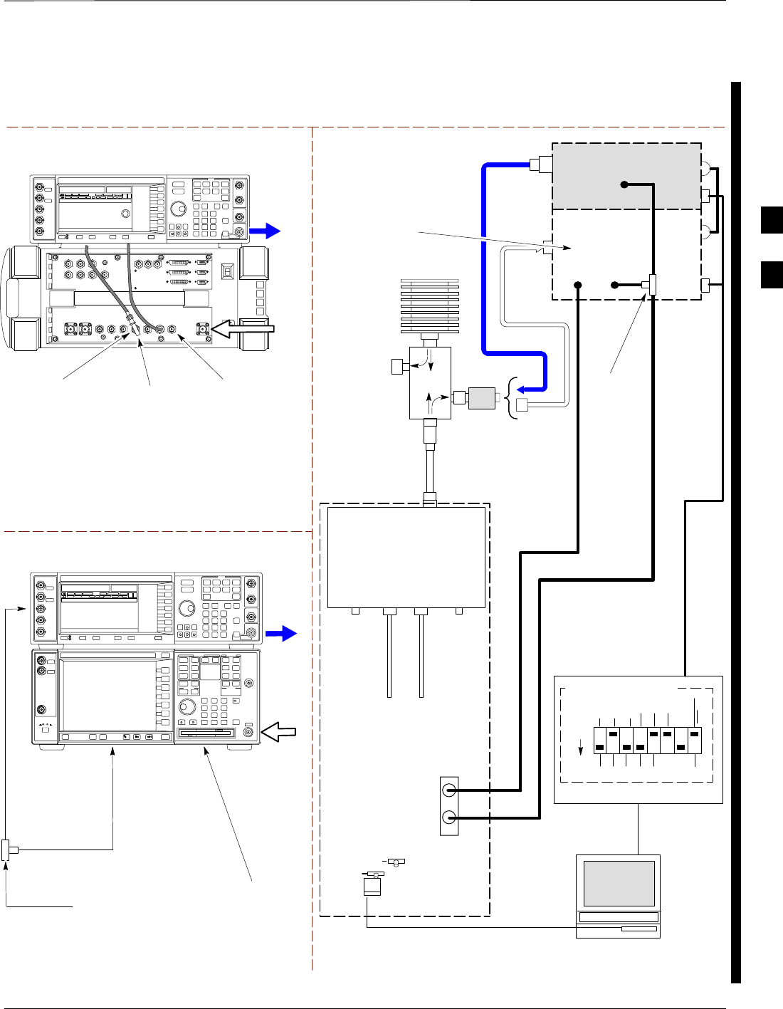
CSM System Time – GPS and HSO Verification – continued
FEB 2005 1X SC 4812T Lite BTS Optimization/ATP 3-73
PRELIMINARY
TEST SETS Optimization/ATP SET–UP
RF INPUT
50 Ω
RF
OUTPUT
50 Ω
Agilent E4432B (Top) and E4406A (Bottom)
FREQ MONITOR
19.6608 MHZ CLOCK
REFERENCE FROM
CSM BOARD
SYNC MONITOR
EVEN SEC TICK
PULSE REFERENCE
FROM CSM BOARD
BNC
“T”
TO TRIGGER IN
ON REAR OF
TRANSMITTER
TESTER
SIGNAL GENERATOR
TO EXT REF IN
ON REAR OF
TRANSMITTER
TESTER
NOTE:
10 MHZ IN ON REAR OF SIGNAL GENERATOR IS CONNECTED TO
10 MHZ OUT (SWITCHED) ON REAR OF TRANSMITTER TESTER.
REFER TO FIGURE F-18.
TO
MPC
TO PA
TRUNKING
MODULE
RS232–GPIB
INTERFACE BOX
INTERNAL PCMCIA
ETHERNET CARD
GPIB
CABLE
UNIVERSAL TWISTED
PAIR (UTP) CABLE
(RJ45 CONNECTORS)
RS232 NULL
MODEM
CABLE
S MODE
DATA FORMAT
BAUD RATE
GPIB ADRS G MODE
ON
BTS
INTERNAL
TX
CABLE
CDMA
LMF
DIP SWITCH SETTINGS *
10BASET/
10BASE2
CONVERTER
LAN
B
LAN
A
Communications
System
Analyzer
HP–IB
OR
GPIB
FREQ
MONITOR
SYNC
MONITOR
CSM
INTERNAL
RX
CABLE
DRF
BTS
CPLD
ANT
CPLD
Signal
Generator
GPIB
10 MHZ
IN
10 MHZ
REF OUT
OR
10 MHZ
OUT
TRIGGER IN
OR
EVEN SEC
SYNCH IN
EXT
REF
IN
BNC
“T”
PATTERN
TRIG IN
* BLACK RECTANGLES
REPRESENT THE RAISED
PART OF SWITCHES
DUPLEXED
TX/RX
ANTENNA
CONNECTOR
RX TEST
CABLE
50 Ω
TERM
.
TX TEST
CABLE
DIRECTIONAL
COUPLER
(30 DB)
100–WATT (MIN.)
NON–RADIATING
RF LOAD
TX TEST
CABLE
2O DB IN–LINE
ATTENUATOR
RF IN/OUT
OR
RF INPUT
50 Ω
RF OUTPUT 50 Ω
IMPORTANT:
WHEN PERFORMING FER TEST ON
COMPANION FRAME DIVERSITY RX,
CONNECT RX TEST CABLE TO
ANTENNA PORT ON COLLOCATED
COMPANION FRAME.
Agilent E4432B (Top) and 8935 Series E6380A
(Bottom)
SYNC MONITOR
EVEN SEC TICK
PULSE REFERENCE
FROM CSM BOARD
FREQ MONITOR
19.6608 MHZ CLOCK
REFERENCE FROM
CSM BOARD
RF
OUTPUT
50 Ω
NOTES:
10 MHZ IN ON REAR OF SIGNAL GENERATOR IS CONNECTED TO
10 MHZ REF OUT ON SIDE OF CDMA BASE STATION TEST SET
PATTERN TRIG IN ON REAR OF SIGNAL GENERATOR IS
CONNECTED TO EVEN SECOND SYNC IN ON SIDE OF CDMA BASE
STATION TEST SET.
(SEE FIGURE F-17)
RF
IN/OUT
BNC
“T”
Figure 3-22: IS–95A/B and CDMA2000 1X ATP Test Set–up With DRFs – Agilent Test Equipment
3

CSM System Time – GPS and HSO Verification – continued
3-74 1X SC 4812T Lite BTS Optimization/ATP FEB 2005
PRELIMINARY
TEST SETS Optimization/ATP SET–UP
INPUT 50 Ω
RF OUT
50 Ω
Advantest R3267 (Top) and R3562 (Bottom)
FREQ MONITOR
19.6608 MHZ CLOCK
REFERENCE FROM
CSM BOARD
SYNC MONITOR
EVEN SEC TICK
PULSE REFERENCE
FROM CSM BOARD
BNC
“T”
NOTE:
SYNTHE REF IN ON REAR OF SIGNAL GENERATOR IS
CONNECTED TO 10 MHZ REF OUT ON REAR OF
SPECTRUM ANALYZER. REFER TO FIGURE F-19)
TO EXT TRIG
ON REAR OF
SPECTRUM
ANALYZER
TO
MPC
TO PA
TRUNKING
MODULE
RS232–GPIB
INTERFACE BOX
INTERNAL PCMCIA
ETHERNET CARD
GPIB
CABLE
UNIVERSAL TWISTED
PAIR (UTP) CABLE
(RJ45 CONNECTORS)
RS232 NULL
MODEM
CABLE
S MODE
DATA FORMAT
BAUD RATE
GPIB ADRS G MODE
ON
BTS
INTERNAL
TX
CABLE
CDMA
LMF
DIP SWITCH SETTINGS
10BASET/
10BASE2
CONVERTER
LAN
B
LAN
A
INPUT
50 Ω
RF OUT
50 Ω
FREQ
MONITOR
SYNC
MONITOR
CSM
INTERNAL
RX
CABLE
DRF
BTS
CPLD
ANT
CPLD
BNC
“T”
Spectrum
Analyzer
GPIB
Signal Generator
GPIB
SYNTHE
REF
IN
10 MHZ
OUT
EXT
TRIG IN
MOD TIME
BASE IN
EXT TRIG
* BLACK RECTANGLES
REPRESENT THE RAISED
PART OF SWITCHES
DUPLEXED
TX/RX
ANTENNA
CONNECTOR
RX TEST
CABLE
50 Ω
TERM
.
TX TEST
CABLE
DIRECTIONAL
COUPLER
(30 DB)
100–WATT (MIN.)
NON–RADIATING
RF LOAD
TX TEST
CABLE
2O DB IN–LINE
ATTENUATOR
IMPORTANT:
WHEN PERFORMING FER TEST ON
COMPANION FRAME DIVERSITY RX,
CONNECT RX TEST CABLE TO
ANTENNA PORT ON COLLOCATED
COMPANION FRAME.
Figure 3-23: IS–95A/B and CDMA2000 1X ATP Test Set–up With DRFs –
Advantest R3267/3562 Test Equipment
3
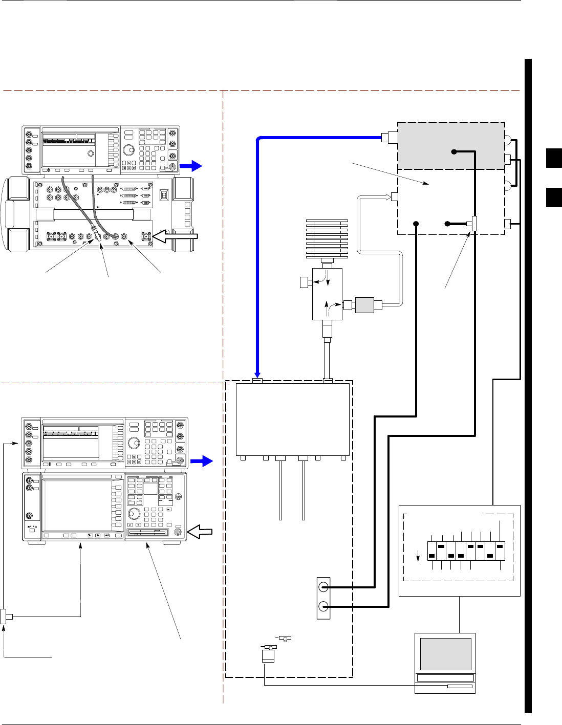
CSM System Time – GPS and HSO Verification – continued
FEB 2005 1X SC 4812T Lite BTS Optimization/ATP 3-75
PRELIMINARY
TEST SETS Optimization/ATP SET–UP
TO
MPC
TO PA
TRUNKING
MODULE
RS232–GPIB
INTERFACE BOX
INTERNAL PCMCIA
ETHERNET CARD
GPIB
CABLE
UNIVERSAL TWISTED
PAIR (UTP) CABLE
(RJ45 CONNECTORS)
RS232 NULL
MODEM
CABLE
S MODE
DATA FORMAT
BAUD RATE
GPIB ADRS G MODE
ON
BTS
INTERNAL
TX
CABLE
CDMA
LMF
DIP SWITCH SETTINGS
10BASET/
10BASE2
CONVERTER
LAN
B
LAN
A
RX TEST
CABLE
Communications
System Analyzer
GPIB
RF IN/OUT
OR RF INPUT 50 Ω
RF OUTPUT 50 Ω
RX
ANTENNA
CONNECTOR
FREQ
MONITOR
SYNC
MONITOR
CSM
INTERNAL
RX
CABLE
TX
ANT
CPLD
RX
BTS
CPLD
TRF
TX
BTS
CPLD
RX
ANT
CPLD
TX
ANTENNA
CONNECTOR
RF INPUT
50 Ω
RF
OUTPUT
50 Ω
Agilent E4432B (Top) and E4406A (Bottom)
FREQ MONITOR
19.6608 MHZ CLOCK
REFERENCE FROM
CSM BOARD
SYNC MONITOR
EVEN SEC TICK
PULSE REFERENCE
FROM CSM BOARD
BNC
“T”
TO TRIGGER IN
ON REAR OF
TRANSMITTER
TESTER
SIGNAL GENERATOR
TO EXT REF IN
ON REAR OF
TRANSMITTER
TESTER
NOTE:
10 MHZ IN ON REAR OF SIGNAL GENERATOR IS CONNECTED TO
10 MHZ OUT (SWITCHED) ON REAR OF TRANSMITTER TESTER.
REFER TO FIGURE F-18.
Signal
Generator
GPIB
10 MHZ
IN
10 MHZ
OUT
50 Ω
TERM
.
TX TEST
CABLE
DIRECTIONAL
COUPLER
(30 DB)
100–WATT (MIN.)
NON–RADIATING
RF LOAD
TRIGGER IN
OR
EVEN SEC
SYNCH IN
EXT
REF
IN
TX TEST
CABLE
BNC
“T”
PATTERN
TRIG IN
* BLACK RECTANGLES
REPRESENT THE RAISED
PART OF SWITCHES
2O DB IN–LINE
ATTENUATOR
IMPORTANT:
WHEN PERFORMING FER TEST ON COMPANION FRAME DIVERSITY RX, CONNECT RX TEST
CABLE TO RX ANTENNA PORT ON COLLOCATED COMPANION FRAME.
Agilent E4432B (Top) and 8935 Series E6380A
(Bottom)
SYNC MONITOR
EVEN SEC TICK
PULSE REFERENCE
FROM CSM BOARD
FREQ MONITOR
19.6608 MHZ CLOCK
REFERENCE FROM
CSM BOARD
RF
OUTPUT
50 Ω
NOTES:
10 MHZ IN ON REAR OF SIGNAL GENERATOR IS CONNECTED TO
10 MHZ REF OUT ON SIDE OF CDMA BASE STATION TEST SET
PATTERN TRIG IN ON REAR OF SIGNAL GENERATOR IS
CONNECTED TO EVEN SECOND SYNC IN ON SIDE OF CDMA BASE
STATION TEST SET.
(SEE FIGURE F-17)
RF
IN/OUT
BNC
“T”
Figure 3-24: IS–95A/B and CDMA2000 1X ATP Test Set–up With TRFs – Agilent Test Equipment
3

CSM System Time – GPS and HSO Verification – continued
3-76 1X SC 4812T Lite BTS Optimization/ATP FEB 2005
PRELIMINARY
TEST SETS Optimization/ATP SET–UP
INPUT 50 Ω
RF OUT
50 Ω
Advantest R3267 (Top) and R3562 (Bottom)
FREQ MONITOR
19.6608 MHZ CLOCK
REFERENCE FROM
CSM BOARD
SYNC MONITOR
EVEN SEC TICK
PULSE REFERENCE
FROM CSM BOARD
BNC
“T”
NOTE:
SYNTHE REF IN ON REAR OF SIGNAL GENERATOR IS
CONNECTED TO 10 MHZ REF OUT ON REAR OF
SPECTRUM ANALYZER. REFER TO FIGURE F-19)
TO EXT TRIG
ON REAR OF
SPECTRUM
ANALYZER
TO
MPC
TO PA
TRUNKING
MODULE
RS232–GPIB
INTERFACE BOX
INTERNAL PCMCIA
ETHERNET CARD
GPIB
CABLE
UNIVERSAL TWISTED
PAIR (UTP) CABLE
(RJ45 CONNECTORS)
RS232 NULL
MODEM
CABLE
S MODE
DATA FORMAT
BAUD RATE
GPIB ADRS G MODE
ON
BTS
INTERNAL
TX
CABLE
CDMA
LMF
DIP SWITCH SETTINGS
10BASET/
10BASE2
CONVERTER
LAN
B
LAN
A
RX TEST
CABLE
Spectrum
Analyzer
GPIB
INPUT
50 Ω
RF OUT
50 Ω
RX
ANTENNA
CONNECTOR
FREQ
MONITOR
SYNC
MONITOR
CSM
INTERNAL
RX
CABLE
TX
ANTENNA
CONNECTOR
Signal Generator
GPIB
SYNTHE
REF
IN
10 MHZ
OUT
50 Ω
TERM
.
TX TEST
CABLE
DIRECTIONAL
COUPLER
(30 DB)
100–WATT (MIN.)
NON–RADIATING
RF LOAD
EXT
TRIG IN
MOD TIME
BASE IN
TX TEST
CABLE
BNC
“T”
EXT TRIG
* BLACK RECTANGLES
REPRESENT THE RAISED
PART OF SWITCHES
TX
ANT
CPLD
RX
BTS
CPLD
TRF
TX
BTS
CPLD
RX
ANT
CPLD
2O DB IN–LINE
ATTENUATOR
IMPORTANT:
WHEN PERFORMING FER TEST ON COMPANION FRAME DIVERSITY RX, CONNECT
RX TEST CABLE TO RX ANTENNA PORT ON COLLOCATED COMPANION FRAME.
Figure 3-25: IS–95A/B and CDMA2000 1X ATP Test Set–up With TRFs –
Advantest R3267/3562 Test Equipment
3

CSM System Time – GPS and HSO Verification – continued
FEB 2005 1X SC 4812T Lite BTS Optimization/ATP 3-77
PRELIMINARY
TEST SET ATP TEST SET–UP
INTERNAL PCMCIA
ETHERNET CARD
UNIVERSAL TWISTED PAIR (UTP)
CABLE (RJ45 CONNECTORS)
BTS
CDMA
LMF
10BASET/
10BASE2
CONVERTER
LAN
B
LAN
A
INTERNAL
ETHERNET
CARD
RF INPUT 50 Ω
OR INPUT 50 Ω
SYNC
MONITOR
CSM
Communications
System Analyzer
50 Ω
TERM
TX TEST
DIRECTIONAL
COUPLER
(30 DB)
100–WATT (MIN.)
NON–RADIATING
RF LOAD TX TEST
NOTE: IF BTS IS EQUIPPED
WITH DUPLEXED RX/TX
SIGNALS, CONNECT THE TX
TEST CABLE TO THE DUPLEXED
ANTENNA CONNECTOR.
2O DB IN–LINE
ATTENUATOR
ETHERNET HUB
RX TEST
RX TEST
RX
ANTENNA
CONNECTOR
TX
ANTENNA
CONNECTOR
TEST
CABLES
NOTE: USE THE SAME
CABLE SET FOR TX AND RX
ATP. SWITCH THE CABLES
DURING ALL ATP TESTS AS
SHOWN.
Power Meter
PORT 2
RF IN
PORT 1
RF OUT
Agilent E7495A
PORT 1
RF OUT
PORT 2
RF IN
SYNC MONITOR
EVEN SEC TICK
PULSE REFERENCE
FROM CSM BOARD
Use only
Agilent supplied
power adapter
GPS
GPIO
Serial 1
Serial 2
Power REF
50 MHz
Sensor
Ext Ref
In
Even Second
Sync In
Antenna
Port 1
RF Out / SWR
Port 2
RF In
Figure 3-26: IS–95A/B and CDMA2000 1X Optimization/ATP Test Set–up – Agilent E7495A
3

Test Equipment Set-up
3-78 1X SC 4812T Lite BTS Optimization/ATP FEB 2005
PRELIMINARY
Connecting Test Equipment to
the BTS
The following types of Test Equipment are required to perform
Calibration and ATP Tests:
SLMF
SCommunications System Analyzer Model supported by the LMF
SPower Meter Model supported by the LMF (required when using the
HP 8921A/600 and Advantest R3465 Analyzers)
SNon–radiating Transmit Line Termination Load
SDirectional Coupler and In–line Attenuator
SRF Cables and Adapters
Refer to Table 3-27 for an overview of Test Equipment Connections for
currently supported by the LMF. In addition, see the following figures:
SFigure 3-31, Figure 3-32, and Figure 3-33 show the Test Set
Connections for TX Calibration
SFigure 3-35 through Figure 3-40 show the Test Set Connections for
Optimization/ATP Tests
Test Equipment GPIB Address
Settings
All Test Equipment is controlled by the LMF through an
IEEE–488/GPIB Bus. To communicate on the Bus, each piece of Test
Equipment must have a GPIB Address Set that the LMF will recognize.
The Standard Address Settings used by the LMF for the various types of
Test Equipment Items are as follows:
SSignal Generator Address: 1
SPower Meter Address: 13
SCommunications System Analyzer Address: 18
Using the procedures included in the Verifying and Setting GPIB
Addresses section of Appendix F, verify and, if necessary, change the
GPIB Address of each piece of employed Test Equipment to match the
applicable addresses above.
Supported Test Equipment
To prevent damage to the Test Equipment, all Transmit
(TX) Test Connections must be through a 30 dB
Directional Coupler plus a 20dB In-line Attenuator for
both the 800 MHz and 1.9 GHz BTSs.
CAUTION
3

Test Equipment Set-up – continued
FEB 2005 1X SC 4812T Lite BTS Optimization/ATP 3-79
PRELIMINARY
IS–95A/B Operation
Optimization and ATP Testing for IS–95A/B Sites and Carriers may be
performed using the following Test Equipment:
SCyberTest
SAdvantest R3267 Spectrum Analyzer with R3562 Signal Generator
SAdvantest R3465 Spectrum Analyzer with R3561L Signal Generator
and HP–437B or Gigatronics Power Meter
SAgilent E4406A Transmitter Test Set with E4432B Signal Generator
SAgilent 8935 Series E6380A Communications Test Set (formerly HP
8935)
SHewlett–Packard HP 8921 (with CDMA Interface and, for 1.9 GHz,
PCS Interface) and HP–437B or Gigatronics Power Meter
SSpectrum Analyzer (HP8594E) – optional
SRubidium Standard Timebase – optional
CDMA2000 1X Operation
Optimization and ATP Testing for CDMA2000 1X Sites and Carriers
may be performed using the following Test Equipment:
SAdvantest R3267 Spectrum Analyzer with R3562 Signal Generator
SAgilent E4406A Transmitter Test Set with E4432B Signal Generator
SAgilent 8935 Series E6380A Communications Test Set (formerly HP
8935) with Option 200 or R2K and with E4432B Signal Generator for
1X FER
SAgilent E7495A Communications Test Set
Test Equipment Preparation
See Appendix F for specific steps to prepare each type of Test Set and
Power Meter to perform Calibration and ATP.
Agilent E7495A Communications Test Set requires additional set–up
and preparation. This is described in detail in Appendix F.
Test Equipment Connection
Charts
To use the following charts to identify necessary Test Equipment
Connections, locate the Communications System Analyzer being used in
the COMMUNICATIONS SYSTEM ANALYZER Columns, and read
down the column. Where a dot appears in the column, connect one end
of the Test Cable to that Connector. Follow the horizontal line to locate
the end connection(s), reading up the column to identify the appropriate
Test Equipment and/or BTS Connector.
3
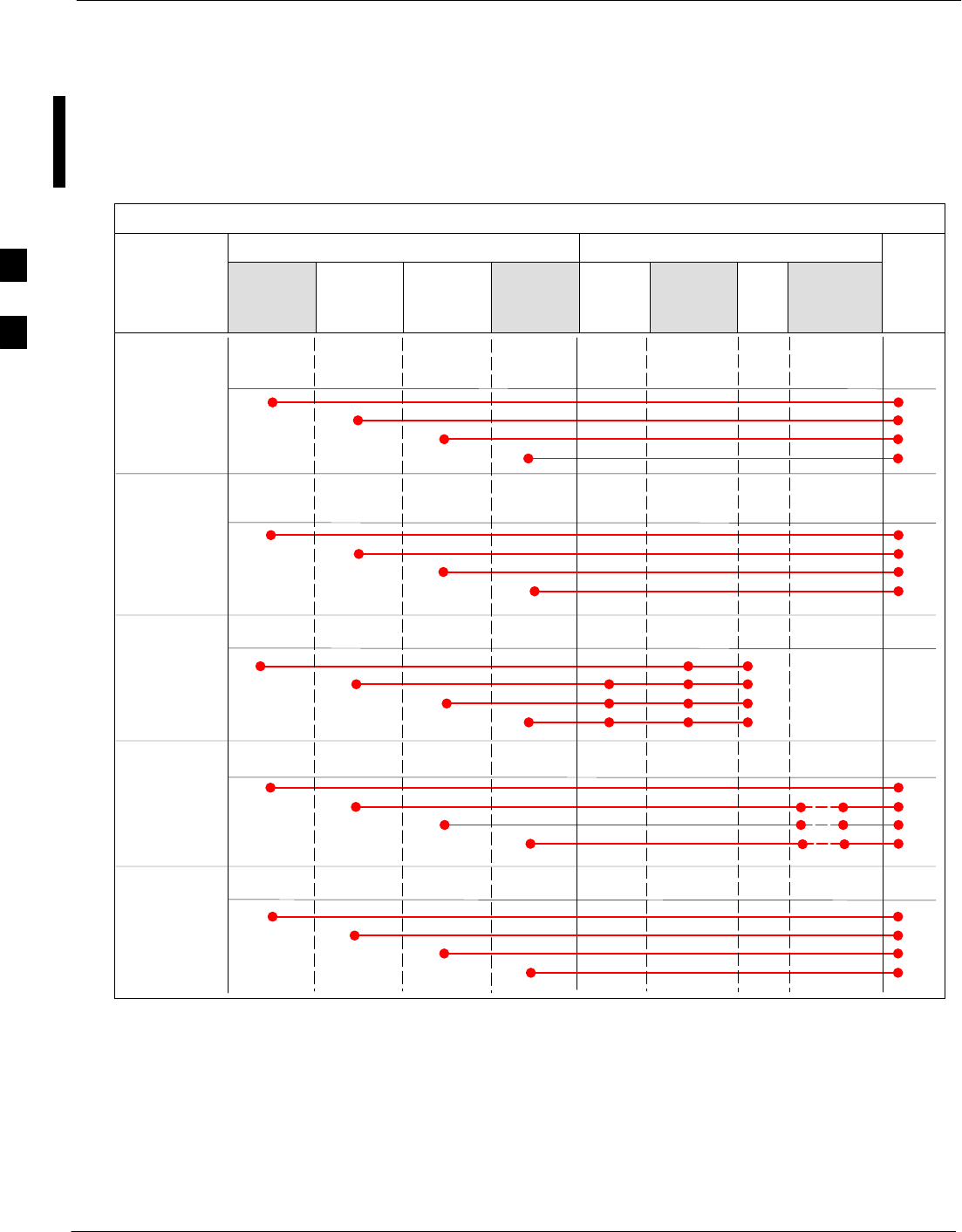
Test Equipment Set-up – continued
3-80 1X SC 4812T Lite BTS Optimization/ATP FEB 2005
PRELIMINARY
IS–95A/B–only Test Equipment Connections
Table 3-27 depicts the Interconnection Requirements for currently
available Test Equipment supporting IS–95A/B only that meets Motorola
Standards and is supported by the LMF.
Table 3-27: IS–95A/B–only Test Equipment Interconnection
COMMUNICATIONS SYSTEM ANALYZER ADDITIONAL TEST EQUIPMENT
SIGNAL Cyber–Test Advantest
R3465 HP 8921A HP 8921
W/PCS Power
Meter GPIB
Interface LMF
Attenuator
and
Directional
Coupler BTS
EVEN SECOND
SYNCHRONIZATION EVEN
SEC REF EVEN SEC
SYNC IN
EVEN
SECOND
SYNC IN
EVEN
SECOND
SYNC IN
19.6608 MHZ
CLOCK TIME
BASE IN
CDMA
TIME BASE
IN
CDMA
TIME BASE
IN
CDMA
TIME BASE
IN
CONTROL
IEEE 488 BUS IEEE
488 GPIB GPIB SERIAL
PORT
HP–I
BHP–IB
TX TEST
CABLES RF
IN/OUT INPUT
50WTX1–6
RF
IN/OUT RF
IN/OUT 20 DB
ATTEN. BTS
PORT
RX TEST
CABLES RF
GEN OUT RF OUT
50WRX1–6
DUPLEX
OUT RF OUT
ONLY
SYNC
MON-
ITOR
FREQ
MON-
ITOR
HP–IB
3

Test Equipment Set-up – continued
FEB 2005 1X SC 4812T Lite BTS Optimization/ATP 3-81
PRELIMINARY
CDMA2000 1X/IS–95A/B–capable Test Equipment
Connections
Table 3-28 depicts the Interconnection Requirements for currently
available Test Equipment supporting both CDMA 2000 1X and
IS–95A/B that meets Motorola Standards and is supported by the LMF.
Table 3-28: CDMA2000 1X/IS–95A/B Test Equipment Interconnection
COMMUNICATIONS SYSTEM ANALYZER ADDITIONAL TEST EQUIPMENT
SIGNAL
Agilent
8935
(Option 200
or R2K) Agilent
E7495A
Advan
test
R3267 Agilent
E4406A Signal
Generator
Advant-
est
R3562
Signal
Genera-
tor Power
Meter
GPIB
Inter-
face LMF
30 dB
Directional
Coupler and
20dB Pad* BTS
EVEN SECOND
SYNCHRONIZATION EXT
TRIG IN EXT
TRIG TRIGGER
IN
19.6608 MHZ
CLOCK MOD TIME
BASE IN EXT REF
IN
CONTROL
IEEE 488 BUS IEEE
488 GPIB HP–IB GPIB SERIAL
PORT
HP–IB
TX TEST
CABLES RF
IN/OUT RF IN TX1–6
RF INPUT
50 OHM 30 DB COUPLER
AND 20 DB PAD
RX TEST
CABLES RF OUT
50 OHM
RF OUT 50
OHM RX1–6
RF OUT
ONLY
SYNC
MONI
TOR
FREQ
MONITOR
PATTERN
TRIG IN
GPIB
RF OUTPUT
50 OHM
RF OUTPUT
50 OHM
10 MHZ IN 10 MHZ OUT
(SWITCHED) 10 MHZ IN
10 MHZ
OUT
10 MHZ
SERIAL
I/O SERIAL
I/O
SIGNAL SOURCE
CONTROLLED
SERIAL I/O
EVEN
SECOND
SYNC IN
EXT REF
IN
HP–IB
RF IN/OUT
DUPLEX
OUT *
SYNTHE
REF IN
* WHEN USED ALONE, THE AGILENT 8935 WITH OPTION 200 OR R2K SUPPORTS IS–95A/B RX TESTING BUT NOT CDMA2000 1X RX TESTING.
EVEN
SECOND
SYNC IN
PORT 1
RF OUT
PORT 2
RF IN
3

Test Equipment Set-up – continued
3-82 1X SC 4812T Lite BTS Optimization/ATP FEB 2005
PRELIMINARY
Equipment Warm-up
To assure BTS stability and contribute to Optimization
accuracy of the BTS, warm-up the BTS Test Equipment
prior to performing the BTS Optimization Procedure as
follows:
– Agilent E7495A for a minimum of 30 minutes
– All other Test Sets for a minimum of 60 minutes
Time spent running initial or normal Power-up, Hardware/
Firmware Audit, and BTS Download counts as Warm-up
Time.
NOTE
Before installing any Test Equipment directly to any BTS
TX OUT Connector, verify that there are no CDMA
Channels keyed.
– At active sites, have the OMC-R/CBSC place the
antenna (sector) assigned to the BBX under test to out
of service (OOS). Failure to do so can result in
serious personal injury and/or equipment damage.
WARNING
Automatic Cable Calibration
Set–up
Figure 3-27 and Figure 3-28 show the Cable Calibration Set–up for the
Test Sets supported by the LMF. The left side of the diagram depicts the
location of the Input and Output Connectors of each Test Equipment
Item, and the right side details the connections for each test. Table 3-32
provides a procedure for performing Automatic Cable Calibration.
Manual Cable Calibration
If Manual Cable Calibration is required, refer to the procedures in
Appendix F.
3

Test Equipment Set-up – continued
FEB 2005 1X SC 4812T Lite BTS Optimization/ATP 3-83
PRELIMINARY
Motorola CyberTest
Advantest Model R3465
RF OUT 50Ω
INPUT 50Ω
RF GEN OUTANT IN
SUPPORTED TEST SETS
100–WATT (MIN)
NON–RADIATING
RF LOAD
TEST
SET
A. SHORT CABLE CAL
SHORT
CABLE
B. RX TEST CAL SET–UP FOR TRF
TEST
SET
C. TX TEST AND DRF RX TEST CAL SET–UP
20DB IN–LINE
ATTENUATOR
CALIBRATION SET–UP
N–N FEMALE
ADAPTER
TX
CABLE
SHORT
CABLE
Note: The 30 dB Directional Coupler is not used
with the Cybertest Test Set. The TX cable is
connected directly to the Cybertest Test Set.
A 10dB Attenuator must be used with the Short
Test Cable for Cable Calibration with the CyberTest
Test Set. The 10dB Attenuator is used only for the
Cable Calibration Procedure, not with the Test
Cables for TX Calibration and ATP Tests.
TEST
SET
RX
CABLE
SHORT
CABLE
DIRECTIONAL
COUPLER
(30 DB)
N–N FEMALE
ADAPTER
50 Ω
ΤERM.
Agilent 8935 Series E6380A
(formerly HP 8935)
RF
IN/OUT
ANT
IN
Hewlett Packard Model HP 8921A
Note: For 800 MHZ only. The HP 8921A cannot
be used to calibrate cables for PCS frequencies.
TX CABLE FOR
TX TEST CABLE
CALIBRATION
RX CABLE FOR DRF
RX TEST
CABLE CALIBRATION
DUPLEX
OUT ANT
IN
Figure 3-27: IS–95A/B Cable Calibration Test Set–up – CyberTest, Agilent 8935, Advantest R3465,
and HP 8921A
3

Test Equipment Set-up – continued
3-84 1X SC 4812T Lite BTS Optimization/ATP FEB 2005
PRELIMINARY
TEST
SET
A. SHORT CABLE CAL
SHORT
CABLE
B. RX TEST SET–UP FOR TRF
CALIBRATION SET–UP
TEST
SET
RX
CABLE
SHORT
CABLE
N–N FEMALE
ADAPTER
SUPPORTED TEST SETS
INPUT 50 Ω
RF OUT
50 Ω
Advantest R3267 (Top) and R3562 (Bottom)
NOTE:
SYNTHE REF IN ON REAR OF SIGNAL GENERATOR IS
CONNECTED TO 10 MHZ OUT ON REAR OF SPECTRUM
ANALYZER
Agilent E4432B (Top) and E4406A (Bottom)
NOTE:
10 MHZ IN ON REAR OF SIGNAL GENERATOR IS CONNECTED TO
10 MHZ OUT (SWITCHED) ON REAR OF TRANSMITTER TESTER
(FIGURE F-18).
RF INPUT
50 Ω
RF OUTPUT
50 Ω
100–WATT (MIN)
NON–RADIATING
RF LOAD
TEST
SET
D. TX TEST SET–UP AND DRF RX TEST
SET–UP
20DB IN–LINE
ATTENUATOR
N–N FEMALE
ADAPTER
TX
CABLE
SHORT
CABLE
DIRECTIONAL
COUPLER
(30 DB)
50 Ω
ΤERM.
TX CABLE FOR
TX TEST CABLE
CALIBRATION
RX CABLE FOR DRF
RX TEST
CABLE CALIBRATION
Figure 3-28: IS–95A/B and CDMA 2000 1X Cable Calibration Test Set–up –
Agilent E4406A/E4432B and Advantest R3267/R3562
3

Test Equipment Set-up – continued
FEB 2005 1X SC 4812T Lite BTS Optimization/ATP 3-85
PRELIMINARY
TEST
SET
A. SHORT CABLE CAL
SHORT
CABLE
B. RX TEST SET–UP FOR TRF
CALIBRATION SET–UP
TEST
SET
RX
CABLE
SHORT
CABLE
N–N FEMALE
ADAPTER
SUPPORTED TEST SETS
Agilent E4432B (Top) and 8935 Series
E6380A (Bottom)
NOTE:
10 MHZ IN ON REAR OF SIGNAL GENERATOR IS CONNECTED TO
10 MHZ REF OUT ON SIDE OF CDMA BASE STATION TEST SET
(FIGURE F-17).
RF OUTPUT
50 Ω
100–WATT (MIN)
NON–RADIATING
RF LOAD
TEST
SET
D. TX TEST SET–UP AND DRF RX TEST
SET–UP
20DB IN–LINE
ATTENUATOR
N–N FEMALE
ADAPTER
TX
CABLE
SHORT
CABLE
DIRECTIONAL
COUPLER
(30 DB)
50 Ω
ΤERM.
TX CABLE FOR
TX TEST CABLE
CALIBRATION
RX CABLE FOR DRF
RX TEST
CABLE CALIBRATION
ANT
IN
Figure 3-29: CDMA2000 1X Cable Calibration Test Set–up – Agilent 8935/E4432B
3

Test Equipment Set-up – continued
3-86 1X SC 4812T Lite BTS Optimization/ATP FEB 2005
PRELIMINARY
TEST
SET
A. SHORT CABLE CAL
SHORT
CABLE
CALIBRATION SET–UP
100–WATT (MIN)
NON–RADIATING
RF LOAD
D. RX and TX TEST SET–UP
20DB IN–LINE
ATTENUATOR
N–N FEMALE
ADAPTER
TX
CABLE
DIRECTIONAL
COUPLER
(30 DB)
50 Ω
ΤERM.
TX CABLE FOR
TX TEST CABLE
CALIBRATION
RX CABLE FOR DRF
RX TEST
CABLE CALIBRATION
10 DB PAD
10 DB PAD
SHORT
CABLE
10 DB PAD
10 DB PAD
TEST
SET
SUPPORTED TEST SETS
Agilent E7495A
PORT 1
RF OUT
PORT 2
RF IN
Use only
Agilent supplied
power adapter
GPS
GPIO
Serial 1
Serial 2
Power REF
50 MHz
Sensor
Ext Ref
In
Even Second
Sync In
Antenna
Port 1
RF Out / SWR
Port 2
RF In
Figure 3-30: CDMA2000 1X Cable Calibration Test Set–up – Agilent E7495A
3

Test Equipment Set-up – continued
FEB 2005 1X SC 4812T Lite BTS Optimization/ATP 3-87
PRELIMINARY
Set-up for TX Calibration
Figure 3-31 and Figure 3-32 show the Test Set Connections for TX
Calibration.
Motorola CyberTest
Agilent 8935 Series E6380A (formerly HP 8935)
TEST SETS TRANSMIT (TX) SET–UP
FRONT PANEL
RF
IN/OUT
RF
IN/OUT
HP–IB
TO GPIB
BOX
NOTE: THE 30 DB DIRECTIONAL COUPLER IS NOT USED WITH THE
CYBERTEST TEST SET. THE TX CABLE IS CONNECTED DIRECTLY
TO THE CYBERTEST TEST SET.
TO
MPC
TO PA
TRUNKING
MODULE
RS232–GPIB
INTERFACE BOX
INTERNAL PCMCIA
ETHERNET CARD
GPIB
CABLE
UNIVERSAL TWISTED PAIR (UTP)
CABLE (RJ45 CONNECTORS)
RS232 NULL
MODEM
CABLE
S MODE
DATA FORMAT
BAUD RATE
GPIB ADRS G MODE
ON
BTS
INTERNAL
TX
CABLE
CDMA
LMF
DIP SWITCH SETTINGS
10BASET/
10BASE2
CONVERTER
LAN
B
LAN
A
GPIB
RF IN/OUT
RX
ANTENNA
CONNECTOR
FREQ
MONITOR
SYNC
MONITOR
CSM
INTERNAL
RX
CABLE
TX
ANT
CPLD
RX
BTS
CPLD
TRF
TX
BTS
CPLD
RX
ANT
CPLD
TX
ANTENNA
CONNECTOR
COMMUNI–
CATIONS
System
Analyzer
2O DB IN–LINE
ATTENUATOR
50 Ω
TERM
.
TX TEST
CABLE
DIRECTIONAL
COUPLER
(30 DB)
100–WATT (MIN.)
NON–RADIATING
RF LOAD
TX TEST
CABLE
* BLACK RECTANGLES
REPRESENT THE RAISED
PART OF SWITCHES
NOTE: IF BTS IS EQUIPPED
WITH DRFS (DUPLEXED
RX/TX SIGNALS), CONNECT
THE TX TEST CABLE TO
THE DRF ANTENNA
CONNECTOR.
POWER
METER
(OPTIONAL)*
POWER
SENSOR
* A POWER METER CAN BE USED IN
PLACE OF THE COMMUNICATIONS
TEST SET FOR TX CALIBRATION/
AUDIT
Figure 3-31: TX Calibration Test Set–up –
CyberTest (IS–95A/B) and Agilent 8935 (IS–95A/B and CDMA2000 1X)
3
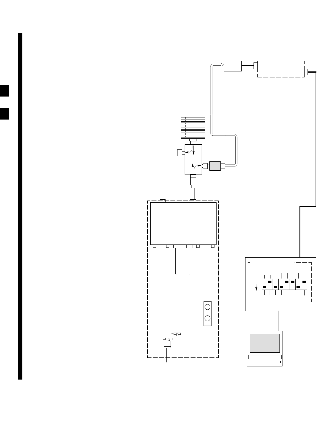
Test Equipment Set-up – continued
3-88 1X SC 4812T Lite BTS Optimization/ATP FEB 2005
PRELIMINARY
TEST SETS TRANSMIT (TX) SET–UP
NOTE: THE HP 8921A AND ADVANTEST
R3465 CANNOT BE USED FOR TX
CALIBRATION. A POWER METER MUST BE
USED.
TO
MPC
TO PA
TRUNKING
MODULE
RS232–GPIB
INTERFACE BOX
INTERNAL PCMCIA
ETHERNET CARD
GPIB
CABLE
UNIVERSAL TWISTED PAIR (UTP)
CABLE (RJ45 CONNECTORS)
RS232 NULL
MODEM
CABLE
S MODE
DATA FORMAT
BAUD RATE
GPIB ADRS G MODE
ON
BTS
INTERNAL
TX
CABLE
CDMA
LMF
DIP SWITCH SETTINGS
10BASET/
10BASE2
CONVERTER
LAN
B
LAN
A
RX
ANTENNA
CONNECTOR
FREQ
MONITOR
SYNC
MONITOR
CSM
INTERNAL
RX
CABLE
TX
ANT
CPLD
RX
BTS
CPLD
TRF
TX
BTS
CPLD
RX
ANT
CPLD
TX
ANTENNA
CONNECTOR
50 Ω
TERM
.
TX TEST
CABLE
DIRECTIONAL
COUPLER
(30 DB)
100–WATT (MIN.)
NON–RADIATING
RF LOAD
TX TEST
CABLE
* BLACK RECTANGLES
REPRESENT THE RAISED
PART OF SWITCHES
NOTE: IF BTS IS EQUIPPED
WITH DRFS (DUPLEXED
RX/TX SIGNALS), CONNECT
THE TX TEST CABLE TO
THE DRF ANTENNA
CONNECTOR.
POWER
SENSOR POWER METER
2O DB IN–LINE
ATTENUATOR
Figure 3-32: TX Calibration Test Set–up – Using Power Meter
3

Test Equipment Set-up – continued
FEB 2005 1X SC 4812T Lite BTS Optimization/ATP 3-89
PRELIMINARY
TEST SETS TRANSMIT (TX) SET–UP
TO
MPC
TO PA
TRUNKING
MODULE
RS232–GPIB
INTERFACE BOX
INTERNAL PCMCIA
ETHERNET CARD
GPIB
CABLE
UNIVERSAL TWISTED PAIR (UTP)
CABLE (RJ45 CONNECTORS)
RS232 NULL
MODEM
CABLE
S MODE
DATA FORMAT
BAUD RATE
GPIB ADRS G MODE
ON
BTS
INTERNAL
TX
CABLE
CDMA
LMF
DIP SWITCH SETTINGS
10BASET/
10BASE2
CONVERTER
LAN
B
LAN
A
GPIB
RF INPUT 50 Ω
OR INPUT 50 Ω
RX
ANTENNA
CONNECTOR
FREQ
MONITOR
SYNC
MONITOR
CSM
INTERNAL
RX
CABLE
TX
ANT
CPLD
RX
BTS
CPLD
TRF
TX
BTS
CPLD
RX
ANT
CPLD
TX
ANTENNA
CONNECTOR
COMMUNI–
CATIONS
System
Analyzer
50 Ω
TERM
.
TX TEST
CABLE
DIRECTIONAL
COUPLER
(30 DB)
100–WATT (MIN.)
NON–RADIATING
RF LOAD
TX TEST
CABLE
* BLACK RECTANGLES
REPRESENT THE RAISED
PART OF SWITCHES
NOTE: IF BTS IS EQUIPPED
WITH DRFS (DUPLEXED
RX/TX SIGNALS), CONNECT
THE TX TEST CABLE TO
THE DRF ANTENNA
CONNECTOR.
POWER
METER
(OPTIONAL)*
POWER
SENSOR
* A POWER METER CAN BE USED IN
PLACE OF THE COMMUNICATIONS
TEST SET FOR TX CALIBRATION/
AUDIT
RF INPUT
50 Ω
Agilent E4406A
INPUT 50 Ω
Advantest R3267
2O DB IN–LINE
ATTENUATOR
Figure 3-33: TX Calibration Test Set–up –
Agilent E4406A and Advantest R3567 (IS–95A/B and CDMA2000 1X)
3
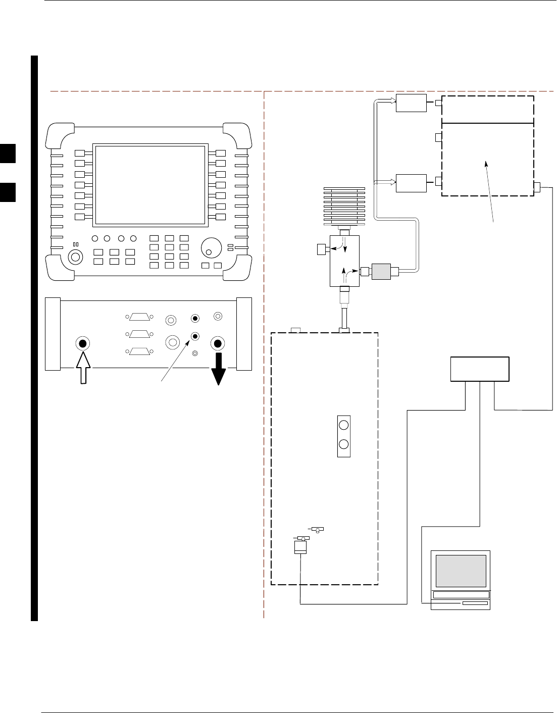
Test Equipment Set-up – continued
3-90 1X SC 4812T Lite BTS Optimization/ATP FEB 2005
PRELIMINARY
TEST SETS TRANSMIT (TX) SET–UP
INTERNAL PCMCIA
ETHERNET CARD
BTS
CDMA
LMF
10BASET/
10BASE2
CONVERTER
LAN
B
LAN
A
RX
ANTENNA
CONNECTOR
SYNC
MONITOR
CSM
TX
ANTENNA
CONNECTOR
50 Ω
TERM
.
TX TEST
CABLE
DIRECTIONAL
COUPLER
(30 DB)
100–WATT (MIN.)
NON–RADIATING
RF LOAD
TX TEST
CABLE
NOTE: IF BTS IS EQUIPPED
WITH DUPLEXED RX/TX
SIGNALS, CONNECT THE TX
TEST CABLE TO THE
DUPLEXED ANTENNA
CONNECTOR.
POWER
SENSOR
2O DB IN–LINE
ATTENUATOR
ETHERNET HUB
UNIVERSAL TWISTED PAIR (UTP)
CABLE (RJ45 CONNECTORS)
Agilent E7495A
PORT 1
RF OUT
PORT 2
RF IN
SYNC MONITOR
EVEN SEC TICK
PULSE REFERENCE
FROM CSM BOARD
Use only
Agilent supplied
power adapter
GPS
GPIO
Serial 1
Serial 2
Power REF
50 MHz
Sensor
Ext Ref
In
Even Second
Sync In
Antenna
Port 1
RF Out / SWR
Port 2
RF In
INTERNAL
ETHERNET
CARD
COMMUNICATIONS
System Analyzer
POWER METER
PORT 2
RF IN
PORT 1
RF OUT
POWER
SENSOR
Figure 3-34: TX Calibration Test Set–up – Agilent E7495A (IS–95A/B and CDMA2000 1X)
3
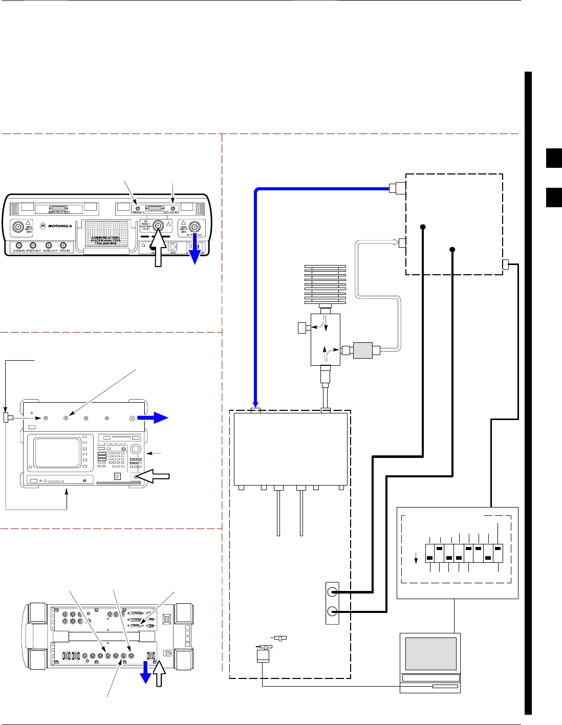
Test Equipment Set-up – continued
FEB 2005 1X SC 4812T Lite BTS Optimization/ATP 3-91
PRELIMINARY
Set–up for ATP Figure 3-35 and Figure 3-36 show the Test Set Connections for ATP Tests.
Motorola CyberTest
TEST SETS Optimization/ATP SET–UP
RF
IN/OUT
SYNC MONITOR
EVEN SEC TICK
PULSE REFERENCE
FROM CSM BOARD
FREQ MONITOR
19.6608 MHZ CLOCK
REFERENCE FROM
CSM BOARD
Advantest Model R3465
INPUT 50Ω
GPIB CONNECTS
TO BACK OF UNIT
NOTE:
The 30 dB Directional Coupler is not used with the
Cybertest Test Set. The TX cable is connected directly to
the Cybertest Test Set.
RF OUT 50Ω
FREQ MONITOR
19.6608 MHZ CLOCK
REFERENCE FROM
CSM BOARD
RF GEN
OUT
SYNC MONITOR EVEN
SEC TICK PULSE
REFERENCE FROM
CSM BOARD
BNC
“T”
TO EXT TRIGGER CONNECTOR
ON REAR OF TEST SET
(FOR DETAILS, SEE
FIGURE F-15)
TO
MPC
TO PA
TRUNKING
MODULE
RS232–GPIB
INTERFACE BOX
INTERNAL PCMCIA
ETHERNET CARD
GPIB
CABLE
UNIVERSAL TWISTED PAIR (UTP)
CABLE (RJ45 CONNECTORS)
RS232 NULL
MODEM
CABLE
S MODE
DATA FORMAT
BAUD RATE
GPIB ADRS G MODE
ON
BTS
INTERNAL
TX
CABLE
CDMA
LMF
DIP SWITCH SETTINGS
10BASET/
10BASE2
CONVERTER
LAN
B
LAN
A
RX TEST
CABLE
GPIB
RF IN/OUT
OR
INPUT 50 Ω
RF GEN OUT,
RF OUT 50Ω,
OR RF IN/OUT
RX
ANTENNA
CONNECTOR
FREQ
MONITOR
SYNC
MONITOR
CSM
INTERNAL
RX
CABLE
TX
ANT
CPLD
RX
BTS
CPLD
TRF
TX
BTS
CPLD
RX
ANT
CPLD
TX
ANTENNA
CONNECTOR
COMMUNICATIONS
System Analyzer
50 Ω
TERM
.
TX TEST
CABLE
DIRECTIONAL
COUPLER
(30 DB)
100–WATT (MIN.)
NON–RADIATING
RF LOAD
TX TEST
CABLE
* BLACK RECTANGLES
REPRESENT THE RAISED
PART OF SWITCHES
CDMA
TIMEBASE
IN
EVEN
SECOND/
SYNC IN
NOTE: IF BTS IS EQUIPPED
WITH DRFS (DUPLEXED RX/TX
SIGNALS), BOTH THE TX AND RX
TEST CABLES CONNECT TO THE
DRF ANTENNA CONNECTOR..
REFER TO FIGURE 3-37.)
2O DB IN–LINE
ATTENUATOR
IMPORTANT:
WHEN PERFORMING FER TEST ON COMPANION FRAME DIVERSITY RX, CONNECT
RX TEST CABLE TO RX ANTENNA PORT ON COLLOCATED COMPANION FRAME.
Agilent 8935 Series E6380A (formerly HP 8935)
RF IN/OUT
HP–IB
TO GPIB
BOX
SYNC MONITOR
EVEN SEC TICK
PULSE REFERENCE
FROM CSM BOARD
FREQ MONITOR
19.6608 MHZ CLOCK
REFERENCE FROM
CSM BOARD
10 MHZ
REF OUT
Figure 3-35: IS–95A/B ATP Test Set–up, TRF Shown – CyberTest, Advantest R3465, and Agilent 8935
3
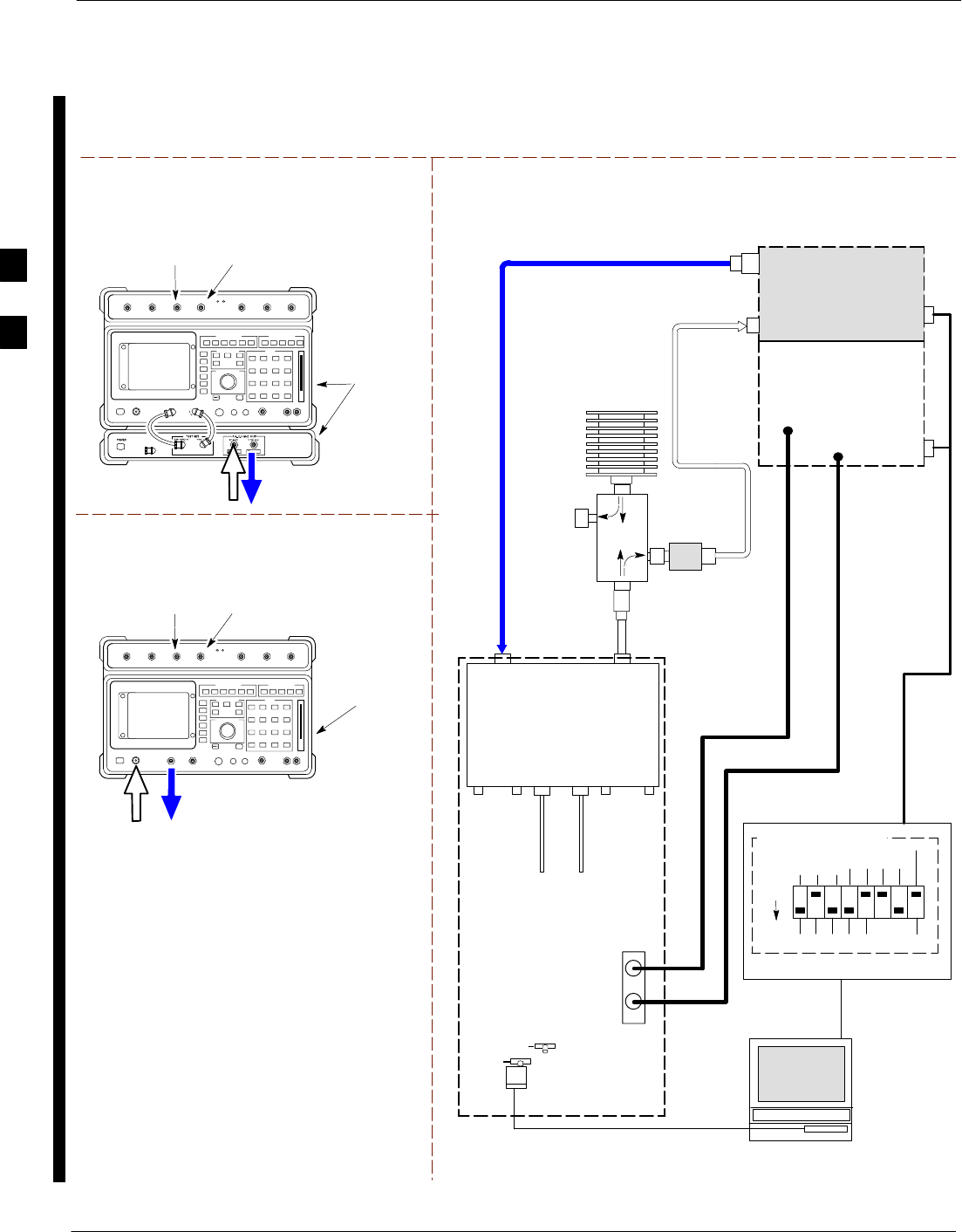
Test Equipment Set-up – continued
3-92 1X SC 4812T Lite BTS Optimization/ATP FEB 2005
PRELIMINARY
RF OUT
ONLY
Hewlett Packard Model HP 8921A W/PCS Interface
(for 1900 MHz)
GPIB
CONNECTS
TO BACK OF
UNITS
SYNC MONITOR
EVEN SEC TICK
PULSE REFERENCE
FROM CSM BOARD
FREQ MONITOR
19.6608 MHZ CLOCK
REFERENCE FROM
CSM BOARD
TEST SETS Optimization/ATP SET–UP
RF
IN/OUT
GPIB
CONNECTS
TO BACK OF
UNIT
SYNC MONITOR
EVEN SEC TICK
PULSE REFERENCE
FROM CSM BOARD
FREQ MONITOR
19.6608 MHZ CLOCK
REFERENCE FROM
CSM BOARD
Hewlett Packard Model HP 8921A
(for 800 MHz)
RF
IN/OUT
DUPLEX
OUT
TO
MPC
TO PA
TRUNKING
MODULE
RS232–GPIB
INTERFACE BOX
INTERNAL PCMCIA
ETHERNET CARD
GPIB
CABLE
UNIVERSAL TWISTED PAIR (UTP)
CABLE (RJ45 CONNECTORS)
RS232 NULL
MODEM
CABLE
S MODE
DATA FORMAT
BAUD RATE
GPIB ADRS G MODE
ON
BTS
INTERNAL
TX
CABLE
CDMA
LMF
DIP SWITCH SETTINGS
10BASET/
10BASE2
CONVERTER
LAN
B
LAN
A
RX TEST
CABLE
GPIB
PCS INTERFACE
INPUT/OUTPUT
PORTS
RX
ANTENNA
CONNECTOR
FREQ
MONITOR
SYNC
MONITOR
CSM
INTERNAL
RX
CABLE
TX
ANT
CPLD
RX
BTS
CPLD
TRF
TX
BTS
CPLD
RX
ANT
CPLD
TX
ANTENNA
CONNECTOR
COMMUNICATIONS
System Analyzer
50 Ω
TERM
.
TX TEST
CABLE
DIRECTIONAL
COUPLER
(30 DB)
100–WATT (MIN.)
NON–RADIATING
RF LOAD
TX TEST
CABLE
* BLACK RECTANGLES
REPRESENT THE RAISED
PART OF SWITCHES
CDMA
TIMEBASE
IN EVEN
SECOND/
SYNC IN
NOTE: IF BTS IS EQUIPPED
WITH DRFS (DUPLEXED
RX/TX SIGNALS), BOTH THE
TX AND RX TEST CABLES
CONNECT TO THE DRF
ANTENNA CONNECTOR..
REFER TO FIGURE 3-37.)
HP PCS
INTERFACE*
2O DB IN–LINE
ATTENUATOR
* FOR 1900 MHZ
ONLY
RF OUT ONLY
RF IN/OUT
NOTE:
FOR 800 MHZ TESTING, CONNECT CABLES TO THE
HP 8921A AS FOLLOWS:
RX TEST CABLE TO DUPLEX OUT
TX TEST CABLE TO RF IN/OUT
IMPORTANT:
WHEN PERFORMING FER TEST ON COMPANION FRAME DIVERSITY RX,
CONNECT RX TEST CABLE TO RX ANTENNA PORT ON COLLOCATED COMPANION
FRAME.
Figure 3-36: IS–95A/B ATP Test Set–up – HP 8921A
3

Test Equipment Set-up – continued
FEB 2005 1X SC 4812T Lite BTS Optimization/ATP 3-93
PRELIMINARY
TEST SETS Optimization/ATP SET–UP
RF INPUT
50 Ω
RF
OUTPUT
50 Ω
Agilent E4432B (Top) and E4406A (Bottom)
FREQ MONITOR
19.6608 MHZ CLOCK
REFERENCE FROM
CSM BOARD
SYNC MONITOR
EVEN SEC TICK
PULSE REFERENCE
FROM CSM BOARD
BNC
“T”
TO TRIGGER IN
ON REAR OF
TRANSMITTER
TESTER
SIGNAL GENERATOR
TO EXT REF IN
ON REAR OF
TRANSMITTER
TESTER
NOTE:
10 MHZ IN ON REAR OF SIGNAL GENERATOR IS CONNECTED TO
10 MHZ OUT (SWITCHED) ON REAR OF TRANSMITTER TESTER.
REFER TO FIGURE F-18.
TO
MPC
TO PA
TRUNKING
MODULE
RS232–GPIB
INTERFACE BOX
INTERNAL PCMCIA
ETHERNET CARD
GPIB
CABLE
UNIVERSAL TWISTED
PAIR (UTP) CABLE
(RJ45 CONNECTORS)
RS232 NULL
MODEM
CABLE
S MODE
DATA FORMAT
BAUD RATE
GPIB ADRS G MODE
ON
BTS
INTERNAL
TX
CABLE
CDMA
LMF
DIP SWITCH SETTINGS *
10BASET/
10BASE2
CONVERTER
LAN
B
LAN
A
Communications
System
Analyzer
HP–IB
OR
GPIB
FREQ
MONITOR
SYNC
MONITOR
CSM
INTERNAL
RX
CABLE
DRF
BTS
CPLD
ANT
CPLD
Signal
Generator
GPIB
10 MHZ
IN
10 MHZ
REF OUT
OR
10 MHZ
OUT
TRIGGER IN
OR
EVEN SEC
SYNCH IN
EXT
REF
IN
BNC
“T”
PATTERN
TRIG IN
* BLACK RECTANGLES
REPRESENT THE RAISED
PART OF SWITCHES
DUPLEXED
TX/RX
ANTENNA
CONNECTOR
RX TEST
CABLE
50 Ω
TERM
.
TX TEST
CABLE
DIRECTIONAL
COUPLER
(30 DB)
100–WATT (MIN.)
NON–RADIATING
RF LOAD
TX TEST
CABLE
2O DB IN–LINE
ATTENUATOR
RF IN/OUT
OR
RF INPUT
50 Ω
RF OUTPUT 50 Ω
IMPORTANT:
WHEN PERFORMING FER TEST ON
COMPANION FRAME DIVERSITY RX,
CONNECT RX TEST CABLE TO
ANTENNA PORT ON COLLOCATED
COMPANION FRAME.
Agilent E4432B (Top) and 8935 Series E6380A
(Bottom)
SYNC MONITOR
EVEN SEC TICK
PULSE REFERENCE
FROM CSM BOARD
FREQ MONITOR
19.6608 MHZ CLOCK
REFERENCE FROM
CSM BOARD
RF
OUTPUT
50 Ω
NOTES:
10 MHZ IN ON REAR OF SIGNAL GENERATOR IS CONNECTED TO
10 MHZ REF OUT ON SIDE OF CDMA BASE STATION TEST SET
PATTERN TRIG IN ON REAR OF SIGNAL GENERATOR IS
CONNECTED TO EVEN SECOND SYNC IN ON SIDE OF CDMA BASE
STATION TEST SET.
(SEE FIGURE F-17)
RF
IN/OUT
BNC
“T”
Figure 3-37: IS–95A/B and CDMA2000 1X ATP Test Set–up With DRFs – Agilent Test Equipment
3
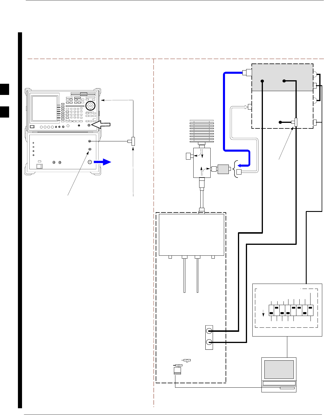
Test Equipment Set-up – continued
3-94 1X SC 4812T Lite BTS Optimization/ATP FEB 2005
PRELIMINARY
TEST SETS Optimization/ATP SET–UP
INPUT 50 Ω
RF OUT
50 Ω
Advantest R3267 (Top) and R3562 (Bottom)
FREQ MONITOR
19.6608 MHZ CLOCK
REFERENCE FROM
CSM BOARD
SYNC MONITOR
EVEN SEC TICK
PULSE REFERENCE
FROM CSM BOARD
BNC
“T”
NOTE:
SYNTHE REF IN ON REAR OF SIGNAL GENERATOR IS
CONNECTED TO 10 MHZ REF OUT ON REAR OF
SPECTRUM ANALYZER. REFER TO FIGURE F-19)
TO EXT TRIG
ON REAR OF
SPECTRUM
ANALYZER
TO
MPC
TO PA
TRUNKING
MODULE
RS232–GPIB
INTERFACE BOX
INTERNAL PCMCIA
ETHERNET CARD
GPIB
CABLE
UNIVERSAL TWISTED
PAIR (UTP) CABLE
(RJ45 CONNECTORS)
RS232 NULL
MODEM
CABLE
S MODE
DATA FORMAT
BAUD RATE
GPIB ADRS G MODE
ON
BTS
INTERNAL
TX
CABLE
CDMA
LMF
DIP SWITCH SETTINGS
10BASET/
10BASE2
CONVERTER
LAN
B
LAN
A
INPUT
50 Ω
RF OUT
50 Ω
FREQ
MONITOR
SYNC
MONITOR
CSM
INTERNAL
RX
CABLE
DRF
BTS
CPLD
ANT
CPLD
BNC
“T”
Spectrum
Analyzer
GPIB
Signal Generator
GPIB
SYNTHE
REF
IN
10 MHZ
OUT
EXT
TRIG IN
MOD TIME
BASE IN
EXT TRIG
* BLACK RECTANGLES
REPRESENT THE RAISED
PART OF SWITCHES
DUPLEXED
TX/RX
ANTENNA
CONNECTOR
RX TEST
CABLE
50 Ω
TERM
.
TX TEST
CABLE
DIRECTIONAL
COUPLER
(30 DB)
100–WATT (MIN.)
NON–RADIATING
RF LOAD
TX TEST
CABLE
2O DB IN–LINE
ATTENUATOR
IMPORTANT:
WHEN PERFORMING FER TEST ON
COMPANION FRAME DIVERSITY RX,
CONNECT RX TEST CABLE TO
ANTENNA PORT ON COLLOCATED
COMPANION FRAME.
Figure 3-38: IS–95A/B and CDMA2000 1X ATP Test Set–up With DRFs –
Advantest R3267/3562 Test Equipment
3

Test Equipment Set-up – continued
FEB 2005 1X SC 4812T Lite BTS Optimization/ATP 3-95
PRELIMINARY
TEST SETS Optimization/ATP SET–UP
TO
MPC
TO PA
TRUNKING
MODULE
RS232–GPIB
INTERFACE BOX
INTERNAL PCMCIA
ETHERNET CARD
GPIB
CABLE
UNIVERSAL TWISTED
PAIR (UTP) CABLE
(RJ45 CONNECTORS)
RS232 NULL
MODEM
CABLE
S MODE
DATA FORMAT
BAUD RATE
GPIB ADRS G MODE
ON
BTS
INTERNAL
TX
CABLE
CDMA
LMF
DIP SWITCH SETTINGS
10BASET/
10BASE2
CONVERTER
LAN
B
LAN
A
RX TEST
CABLE
Communications
System Analyzer
GPIB
RF IN/OUT
OR RF INPUT 50 Ω
RF OUTPUT 50 Ω
RX
ANTENNA
CONNECTOR
FREQ
MONITOR
SYNC
MONITOR
CSM
INTERNAL
RX
CABLE
TX
ANT
CPLD
RX
BTS
CPLD
TRF
TX
BTS
CPLD
RX
ANT
CPLD
TX
ANTENNA
CONNECTOR
RF INPUT
50 Ω
RF
OUTPUT
50 Ω
Agilent E4432B (Top) and E4406A (Bottom)
FREQ MONITOR
19.6608 MHZ CLOCK
REFERENCE FROM
CSM BOARD
SYNC MONITOR
EVEN SEC TICK
PULSE REFERENCE
FROM CSM BOARD
BNC
“T”
TO TRIGGER IN
ON REAR OF
TRANSMITTER
TESTER
SIGNAL GENERATOR
TO EXT REF IN
ON REAR OF
TRANSMITTER
TESTER
NOTE:
10 MHZ IN ON REAR OF SIGNAL GENERATOR IS CONNECTED TO
10 MHZ OUT (SWITCHED) ON REAR OF TRANSMITTER TESTER.
REFER TO FIGURE F-18.
Signal
Generator
GPIB
10 MHZ
IN
10 MHZ
OUT
50 Ω
TERM
.
TX TEST
CABLE
DIRECTIONAL
COUPLER
(30 DB)
100–WATT (MIN.)
NON–RADIATING
RF LOAD
TRIGGER IN
OR
EVEN SEC
SYNCH IN
EXT
REF
IN
TX TEST
CABLE
BNC
“T”
PATTERN
TRIG IN
* BLACK RECTANGLES
REPRESENT THE RAISED
PART OF SWITCHES
2O DB IN–LINE
ATTENUATOR
IMPORTANT:
WHEN PERFORMING FER TEST ON COMPANION FRAME DIVERSITY RX, CONNECT RX TEST
CABLE TO RX ANTENNA PORT ON COLLOCATED COMPANION FRAME.
Agilent E4432B (Top) and 8935 Series E6380A
(Bottom)
SYNC MONITOR
EVEN SEC TICK
PULSE REFERENCE
FROM CSM BOARD
FREQ MONITOR
19.6608 MHZ CLOCK
REFERENCE FROM
CSM BOARD
RF
OUTPUT
50 Ω
NOTES:
10 MHZ IN ON REAR OF SIGNAL GENERATOR IS CONNECTED TO
10 MHZ REF OUT ON SIDE OF CDMA BASE STATION TEST SET
PATTERN TRIG IN ON REAR OF SIGNAL GENERATOR IS
CONNECTED TO EVEN SECOND SYNC IN ON SIDE OF CDMA BASE
STATION TEST SET.
(SEE FIGURE F-17)
RF
IN/OUT
BNC
“T”
Figure 3-39: IS–95A/B and CDMA2000 1X ATP Test Set–up With TRFs – Agilent Test Equipment
3
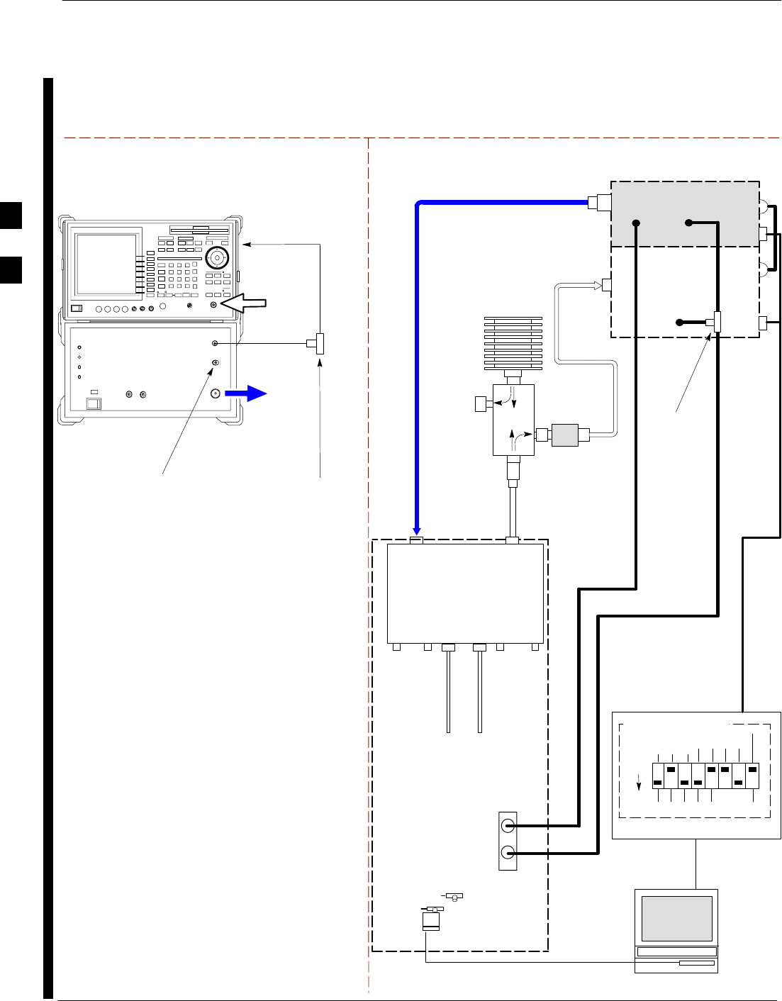
Test Equipment Set-up – continued
3-96 1X SC 4812T Lite BTS Optimization/ATP FEB 2005
PRELIMINARY
TEST SETS Optimization/ATP SET–UP
INPUT 50 Ω
RF OUT
50 Ω
Advantest R3267 (Top) and R3562 (Bottom)
FREQ MONITOR
19.6608 MHZ CLOCK
REFERENCE FROM
CSM BOARD
SYNC MONITOR
EVEN SEC TICK
PULSE REFERENCE
FROM CSM BOARD
BNC
“T”
NOTE:
SYNTHE REF IN ON REAR OF SIGNAL GENERATOR IS
CONNECTED TO 10 MHZ REF OUT ON REAR OF
SPECTRUM ANALYZER. REFER TO FIGURE F-19)
TO EXT TRIG
ON REAR OF
SPECTRUM
ANALYZER
TO
MPC
TO PA
TRUNKING
MODULE
RS232–GPIB
INTERFACE BOX
INTERNAL PCMCIA
ETHERNET CARD
GPIB
CABLE
UNIVERSAL TWISTED
PAIR (UTP) CABLE
(RJ45 CONNECTORS)
RS232 NULL
MODEM
CABLE
S MODE
DATA FORMAT
BAUD RATE
GPIB ADRS G MODE
ON
BTS
INTERNAL
TX
CABLE
CDMA
LMF
DIP SWITCH SETTINGS
10BASET/
10BASE2
CONVERTER
LAN
B
LAN
A
RX TEST
CABLE
Spectrum
Analyzer
GPIB
INPUT
50 Ω
RF OUT
50 Ω
RX
ANTENNA
CONNECTOR
FREQ
MONITOR
SYNC
MONITOR
CSM
INTERNAL
RX
CABLE
TX
ANTENNA
CONNECTOR
Signal Generator
GPIB
SYNTHE
REF
IN
10 MHZ
OUT
50 Ω
TERM
.
TX TEST
CABLE
DIRECTIONAL
COUPLER
(30 DB)
100–WATT (MIN.)
NON–RADIATING
RF LOAD
EXT
TRIG IN
MOD TIME
BASE IN
TX TEST
CABLE
BNC
“T”
EXT TRIG
* BLACK RECTANGLES
REPRESENT THE RAISED
PART OF SWITCHES
TX
ANT
CPLD
RX
BTS
CPLD
TRF
TX
BTS
CPLD
RX
ANT
CPLD
2O DB IN–LINE
ATTENUATOR
IMPORTANT:
WHEN PERFORMING FER TEST ON COMPANION FRAME DIVERSITY RX, CONNECT
RX TEST CABLE TO RX ANTENNA PORT ON COLLOCATED COMPANION FRAME.
Figure 3-40: IS–95A/B and CDMA2000 1X ATP Test Set–up With TRFs –
Advantest R3267/3562 Test Equipment
3
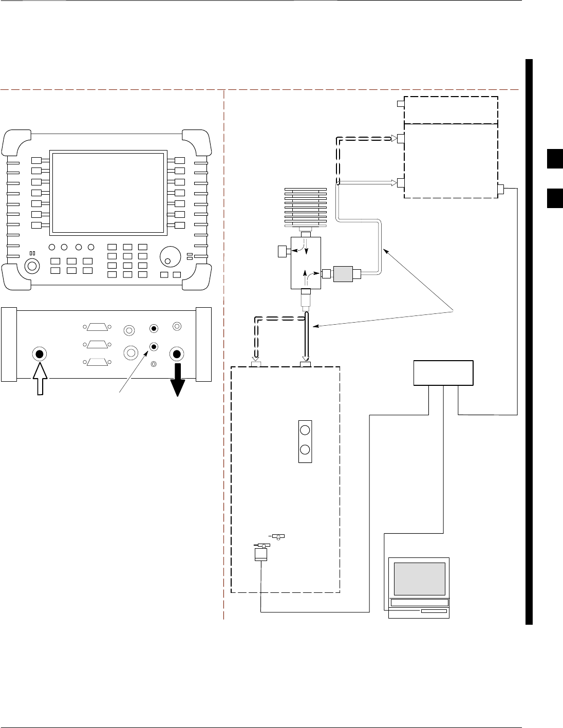
Test Equipment Set-up – continued
FEB 2005 1X SC 4812T Lite BTS Optimization/ATP 3-97
PRELIMINARY
TEST SET ATP TEST SET–UP
INTERNAL PCMCIA
ETHERNET CARD
UNIVERSAL TWISTED PAIR (UTP)
CABLE (RJ45 CONNECTORS)
BTS
CDMA
LMF
10BASET/
10BASE2
CONVERTER
LAN
B
LAN
A
INTERNAL
ETHERNET
CARD
RF INPUT 50 Ω
OR INPUT 50 Ω
SYNC
MONITOR
CSM
Communications
System Analyzer
50 Ω
TERM
TX TEST
DIRECTIONAL
COUPLER
(30 DB)
100–WATT (MIN.)
NON–RADIATING
RF LOAD TX TEST
NOTE: IF BTS IS EQUIPPED
WITH DUPLEXED RX/TX
SIGNALS, CONNECT THE TX
TEST CABLE TO THE DUPLEXED
ANTENNA CONNECTOR.
2O DB IN–LINE
ATTENUATOR
ETHERNET HUB
RX TEST
RX TEST
RX
ANTENNA
CONNECTOR
TX
ANTENNA
CONNECTOR
TEST
CABLES
NOTE: USE THE SAME
CABLE SET FOR TX AND RX
ATP. SWITCH THE CABLES
DURING ALL ATP TESTS AS
SHOWN.
Power Meter
PORT 2
RF IN
PORT 1
RF OUT
Agilent E7495A
PORT 1
RF OUT
PORT 2
RF IN
SYNC MONITOR
EVEN SEC TICK
PULSE REFERENCE
FROM CSM BOARD
Use only
Agilent supplied
power adapter
GPS
GPIO
Serial 1
Serial 2
Power REF
50 MHz
Sensor
Ext Ref
In
Even Second
Sync In
Antenna
Port 1
RF Out / SWR
Port 2
RF In
Figure 3-41: IS–95A/B and CDMA2000 1X Optimization/ATP Test Set–up – Agilent E7495A
3

Test Set Calibration
3-98 1X SC 4812T Lite BTS Optimization/ATP FEB 2005
PRELIMINARY
Test Equipment Calibration
Background
Proper Test Equipment Calibration helps to ensure accurate BTS
Optimization and Acceptance Testing by assuring that the Test
Equipment and associated cables do not introduce Measurement Errors.
If the Test Equipment Set being used to optimize or test the
BTS has been calibrated and maintained as a set, this
procedure does not need to be performed.
NOTE
This procedure must be performed prior to beginning the Optimization.
Verify that all Test Equipment (including all associated cables and
adapters actually used to interconnect Test Equipment Items and the
BTS) has been calibrated and maintained as a set.
If any piece of Test Equipment, Test Cable, or RF Adapter
that makes up the calibrated Test Equipment Set has been
replaced, the set must be re-calibrated.
– Failure to do so can introduce Measurement Errors,
resulting in incorrect measurements and degradation
to system performance.
– Motorola recommends repeating Cable Calibration
before testing at each BTS Site.
CAUTION
Calibration of the Communications System Analyzer (or
equivalent Test Equipment) must be performed at the site
before calibrating the overall Test Equipment Set.
– Calibrate the Test Equipment after it has been
allowed to warm–up and stabilize for a a minimum of
60 minutes.
NOTE
Automatic Calibration
Procedure
Procedures included in this section use the LMF Automated Calibration
Procedure to determine Path Losses of the supported Communications
Analyzer, Power Meter, associated Test Cables, Adapters, and (if used)
Antenna Switch that make up the overall calibrated Test Equipment Set.
After Calibration, the Gain/Loss Offset Values are stored in a Test
Measurement Offset File on the LMF Computer.
3

Test Set Calibration – continued
FEB 2005 1X SC 4812T Lite BTS Optimization/ATP 3-99
PRELIMINARY
Manual Calibration Procedures
Agilent E4406A Transmitter Tester
The E4406A does not support the Power Level Zeroing Calibration
performed by the LMF. If this instrument is to be used for Bay Level
Offset Calibration and Calibration is attempted with the LMF Calibrate
Test Equipment Function, the LMF will return a Failure Message
Status Window stating that Zeroing Power is not supported by the
E4406A.
– Refer to the Equipment Calibration section of Appendix F for
instructions on using the instrument’s Self–alignment (Calibration)
Function prior to performing Bay Level Offset Calibration..
Power Meters
Manual Power Meter Calibration Procedures to be performed prior to
automated Calibration are included in the Equipment Calibration section
of Appendix F..
Cable Calibration
Manual Cables using the HP 8921A and Advantest R3465
Communications System Analyzers are provided in the Manual Cable
Calibration section of Appendix F, if needed..
GPIB Addresses
GPIB Addresses can range from 1 through 30. The LMF will accept any
address in that range, but the numbers entered in the LMF Options
Window GPIB Address Boxes (Table 3-29 and Table 3-30) must match
the addresses set in the Test Equipment. Motorola recommends using 1
for a CDMA Signal Generator, 13 for a Power Meter, and 18 for a
Communications System Analyzer. To verify and, if necessary, change
the GPIB Addresses of the Test Equipment, refer to the Setting GPIB
Addresses section of Appendix F.
IP Addresses
For the Agilent E7495A Communications Test Set, set the IP Address
and complete Initial Set–up as described in Appendix F. Specifically, see
Table F-1 on Page F-1.
Selecting Test Equipment
Serial Connection and Network Connection Tabs are provided in the
LMF Options Window to specify the Test Equipment Connection
Method.
– The Serial Connection Tab is used when the Test Equipment Items
are connected directly to the LMF Computer through a GPIB Box
(normal set–up).
– The Network Connection Tab is used when the Test Equipment is
to be connected remotely via a Network Connection or the Agilent
E7495A Communications Test Set is used. Refer to Appendix F.
Specifically, see Table F-1 on Page F-1.
3

Test Set Calibration – continued
3-100 1X SC 4812T Lite BTS Optimization/ATP FEB 2005
PRELIMINARY
Prerequisites
Ensure that the following have been completed before selecting Test
Equipment:
STest Equipment is turned on.
SGPIB Addresses set in the Test Equipment have been verified as
correct using the applicable procedures in Appendix F. (Not required
with Agilent E7495A.)
SLMF Computer Serial Port and Test Equipment are connected to the
GPIB Box. (GPIB not applicable with Agilent E7495A)
Selecting Test Equipment
Test Equipment may be selected either manually with operator input or
automatically using the LMF autodetect feature.
Manually Selecting Test
Equipment in a Serial
Connection Tab
Test Equipment can be manually specified before or after the Test
Equipment is connected. The LMF does not attempt to verify that the
Test Equipment is actually detected when Manual Selection is specified.
Perform the procedure in Table 3-29 to manually select Test Equipment.
Table 3-29: Selecting Test Equipment Manually in the Serial Connection Tab Procedure
nStep Action
1In the LMF Window Menu Bar, click Tools and select Options... from the Pull–down Menu.
– The LMF Options Window appears.
– If it is not in the forefront, click on the Serial Connection Tab.
2Select the correct Serial Port in the COMM Port: Pick List (normally COM1).
–If it is not selected (no black dot showing), click on the Manual Specification Button.
3Click on the Check Box(es) corresponding to the Test Equipment Item(s) to be used.
table continued on next page
3

Test Set Calibration – continued
FEB 2005 1X SC 4812T Lite BTS Optimization/ATP 3-101
PRELIMINARY
Table 3-29: Selecting Test Equipment Manually in the Serial Connection Tab Procedure
nActionStep
4Type the GPIB Address in the corresponding GPIB Address Box.
– Refer to the Setting GPIB Addresses section of Appendix F for directions on verifying and/or
changing Test Equipment GPIB Addresses.
Motorola–recommended addresses are:
–1 = Signal Generator
–13 = Power Meter
–18 = Communications System Analyzer
NOTE
When Test Equipment Items are manually selected by the operator, the LMF defaults to using a
Power Meter for RF Power Measurements. The LMF will use a Communications System
Analyzer for RF Power Measurements only if a Power Meter is not selected (Power Meter Check
Box not checked).
5Click on Apply.
– The button will darken until the selection has been recorded.
NOTE
With Manual Selection, the LMF does not attempt to detect the Test Equipment to verify it is
connected and communicating with the LMF.
6Click on Dismiss to close the LMF Options Window.
3

Test Set Calibration – continued
3-102 1X SC 4812T Lite BTS Optimization/ATP FEB 2005
PRELIMINARY
Automatically Selecting Test
Equipment in the Serial
Connection Tab When using the Auto–detection Feature to select Test Equipment, the
LMF determines which Test Equipment Items are actually
communicating with LMF. Perform the procedure in Table 3-30 to use
the Auto–detection Feature.
Table 3-30: Selecting Test Equipment Using Auto-Detect Procedure
nStep Action
NOTE
An alternate procedure is required if using the Agilent E7495A Test Set.
– See “Detecting Test Equipment when using Agilent E7495A” topic following this
table.
1In the LMF Window Menu Bar, click Tools and select Options... from the Pull–down Menu.
– The LMF Options Window appears.
– If it is not in the forefront, click on the Serial Connection Tab.
2Select the correct Serial Port in the COMM Port: Pick List (normally COM1).
SIf it is not selected (no black dot showing), click on the Auto–Detection Button.
SIf they are not already displayed in the box labeled GPIB Address to search, click in the box
and type in the GPIB Addresses for the Test Equipment to be used, separating each address with
commas and no spaces.
– Refer to the Setting GPIB Addresses section of Appendix F for instructions on verifying
and/or changing Test Equipment GPIB Addresses.
* IMPORTANT
During the GPIB Address search for a Test Equipment Item to perform RF Power Measurements
(that is, for TX Calibration), the LMF will select the first item it finds with the capability to
perform the measurement.
SIf, for example, the address sequence 13,18,1 is included in the GPIB Addresses to search
Box, the Power Meter (GPIB Address 13) will be used for RF Power Measurements.
SIf the address sequence 18,13,1 is included, the LMF will use the Communications System
Analyzer (GPIB Address 18) for Power Measurements.
3 Click Apply.
– The button will darken until the selection has been recorded.
– A Check Mark will appear in the applicable Manual Configuration section.
4Check the boxes for detected Test Equipment Items.
5 Click Dismiss to close the LMF Options Window.
3
Test Set Calibration – continued
FEB 2005 1X SC 4812T Lite BTS Optimization/ATP 3-103
PRELIMINARY
Detecting Test Equipment
when using Agilent E7495A
Verify that no other equipment is connected to the LMF.
IMPORTANT
*
Agilent E7495A equipment must be connected to the LAN to detect it.
Then perform the procedures described in Appendix F. Specifically, refer
to Table F-1 on Page F-1, Table F-2, and Table F-3 on Page F-3.
Calibrating Test Equipment
The LMF Calibrate Test Equipment Procedure zeros the Power
Measurement Level of the Test Equipment Item that is to be used for TX
Calibration and Audit. If both a Power Meter and an Analyzer are
connected (for example, an HP 437 and an HP 8921A/600), only the
Power Meter is Zeroed.
The Agilent E4406A Transmitter Tester does not support
Power Measurement Level zeroing.
– Refer to the Equipment Calibration section of
Appendix F for Agilent E4406A Calibration.
NOTE
Prerequisites
SLMF Computer Serial Port and Test Equipment are connected to the
GPIB Box.
STest Equipment is turned on and has warmed–up for at least 60
minutes.
STest Equipment has been selected in the LMF (Table 3-29 or
Table 3-30)
Perform the procedure in Table 3-31 to calibrate the Test Equipment.
Table 3-31: LMF Test Equipment Calibration Procedure
nStep Action
1From the Util Menu, select Calibrate Test Equipment from the Pull–down Menu.
–A Directions Window is displayed.
2Follow the directions provided.
3Click on Continue to close the Directions Window and start the Calibration Process.
–A Status Report Window is displayed.
4Click on OK to close the Status Report Window.
3

Test Set Calibration – continued
3-104 1X SC 4812T Lite BTS Optimization/ATP FEB 2005
PRELIMINARY
LMF Cables Calibration
Overview
The LMF Cable Calibration Function is used to measure the Path Loss
(in dB) for the TX and RX Cables, Adapters, Directional Couplers, and
Attenuators that make up the Cable Configurations used for testing. A
Communications System Analyzer is used to measure the Signal Loss of
both the TX Test Cable and the RX Test Cable Configurations. The LMF
Cable Calibration consists of the following processes:
Measure the Signal Loss in a Short Cable
This measurement is done to compensate for any Measurement Error in
the Communications System Analyzer. The Short Test Cable, which is
used only for the Calibration Process, is connected in series with both
the TX and RX Test Cable Configurations when they are measured.
The measured Signal Loss in the Short Test Cable is deducted from the
measured Signal Loss of the TX and RX Test Cable Configurations to
determine the actual loss of the configurations. This deduction is done so
that any error in the analyzer measurement can be adjusted out of both
the TX and RX Measurements.
Measure the Signal Loss in the Short Cable plus the RX Test
Cable Configuration
The RX Test Cable Configuration normally consists only of a COAX
Cable with Type–N Connectors that is long enough to reach from the
BTS RX Connector to the Test Equipment.
When the BTS Antenna Connectors carry Duplexed TX and RX Signals,
a Directional Coupler is required. If required by BTS Type, an additional
Attenuator is also required for the RX Test Cable Configuration. These
additional items must be included in the Path Loss Measurement.
Measure the Signal Loss in the Short Cable plus the TX Test
Cable Configuration
The TX Test Cable Configuration normally consists of two COAX
Cables with Type–N Connectors, a Directional Coupler, a Termination
Load with sufficient rating to dissipate the BTS Output Power, and an
additional Attenuator, if required by the BTS Type.
The total Path Loss of the TX Test Configuration must be as required for
the BTS (normally 30 or 50 dB). The Motorola CyberTest Analyzer is
different from other Communications System Analyzers because the
required Attenuation/Load is built into the Test Set. Because of this, the
Cybertest TX Test Configuration consists only of the required length
COAX Cable.
3
Test Set Calibration – continued
FEB 2005 1X SC 4812T Lite BTS Optimization/ATP 3-105
PRELIMINARY
Calibrating Test Cabling using
a Communications System
Analyzer
Prerequisites
STest Equipment is turned on and has warmed–up for at least 60
minutes.
STest Equipment has been selected in the LMF (Table 3-29 or
Table 3-30).
STest Equipment has been calibrated and correctly connected for the
type of Test Cable Configuration to be calibrated.
LMF Cable Calibration cannot be accomplished with an
HP 8921A Analyzer for 1.9 GHz. A different analyzer
type or the Signal Generator and Spectrum Analyzer
Method (Table 3-33 and Table 3-34) must be used.
Cable Calibration Values must be manually entered into
the LMF Test Cable Insertion Loss File if the Signal
Generator and Spectrum Analyzer Method is used.
To use the HP 8921A for Manual Test Cable
Configuration Calibration for 800 MHz BTSs, refer to the
Manual Cable Calibration section of Appendix F.
NOTE
Procedure
Refer to Figure 3-12, Figure 3-13, or Figure 3-14 and perform the
procedure in Table 3-32 to calibrate the Test Cable Configurations.
Table 3-32: Test Cabling Calibration using Communications System Analyzer Procedure
nStep Action
1 Click Util in the BTS Menu Bar, and select Cable Calibration... in the Pull–down Menu.
–A Cable Calibration Window is displayed.
2Enter one or more Channel Numbers in the Channels Box.
NOTE
Multiple Channel Numbers must be separated by a comma with no spaces (for example,
200,800).
– When two or more Channel Numbers are entered, the cables are calibrated for each channel.
– Interpolation is accomplished for other channels, as required, for TX Calibration.
table continued on next page
3
Test Set Calibration – continued
3-106 1X SC 4812T Lite BTS Optimization/ATP FEB 2005
PRELIMINARY
Table 3-32: Test Cabling Calibration using Communications System Analyzer Procedure
nActionStep
3 Select:
–TX and RX CABLE CAL, TX CABLE CAL
or
–RX CABLE CAL
in the Cable Calibration Pick List.
4 Click OK, and follow the directions displayed for each step.
– A Status Report Window will be displayed with the results of the Cable Calibration.
3

Test Set Calibration – continued
FEB 2005 1X SC 4812T Lite BTS Optimization/ATP 3-107
PRELIMINARY
Calibrate Test Cabling using a
Signal Generator and Spectrum
Analyzer
Refer to Figure 3-42 and perform the procedure in Table 3-33 to calibrate
the TX Test Cable Configuration for all BTSs or the RX ATP Test Cable
Configuration for BTSs with Duplexed TX/RX using the Signal
Generator and Spectrum Analyzer.
Refer to Figure 3-43 and perform the procedure in Table 3-34 to calibrate
the Test Cable Configuration for non–Duplexed RX using the Signal
Generator and Spectrum Analyzer.
TX and Duplexed RX Cable Calibration
Table 3-33: TX/Duplexed RX Test Cabling using Signal Generator and Spectrum Analyzer
Calibration Procedure
nStep Action
1Connect a Short Test Cable between the Spectrum Analyzer and the Signal Generator as shown in
Figure 3-42, Detail “A” (top portion of figure).
2Set the Signal Generator to 0 dBm at the Customer Frequency.
– 869.7–893.31 MHz for North American Cellular
or
– 1930–1990 MHz for North American PCS
3Use Spectrum Analyzer to measure the Signal Generator Output.
4Record the value for the Detail “A” Set–up.
5Change the Test Set–up to the one shown in Detail “B” (lower portion of Figure 3-42), to measure
Cable Output at the Customer Frequency.
– 869.7–893.31 MHz for North American Cellular
or
– 1930–1990 MHz for North American PCS
6Record the value measured using the Detail “B” Test Set–up.
7Calibration Factor = (Value measured with Detail “A” Set–up) – (Value measured with Detail “B”
Set–up)
Example: Calibration Factor = –1 dBm – (–53.5 dBm) = 52.5 dBm
* IMPORTANT
The Short Test Cable is used for Calibration Only.
– It is not part of the Final Test Set–up.
After Calibration is completed, do not re-arrange any cables.
– Use the Test Cable Configuration as–is to ensure that the Test Procedures use the correct
Calibration Factor.
3
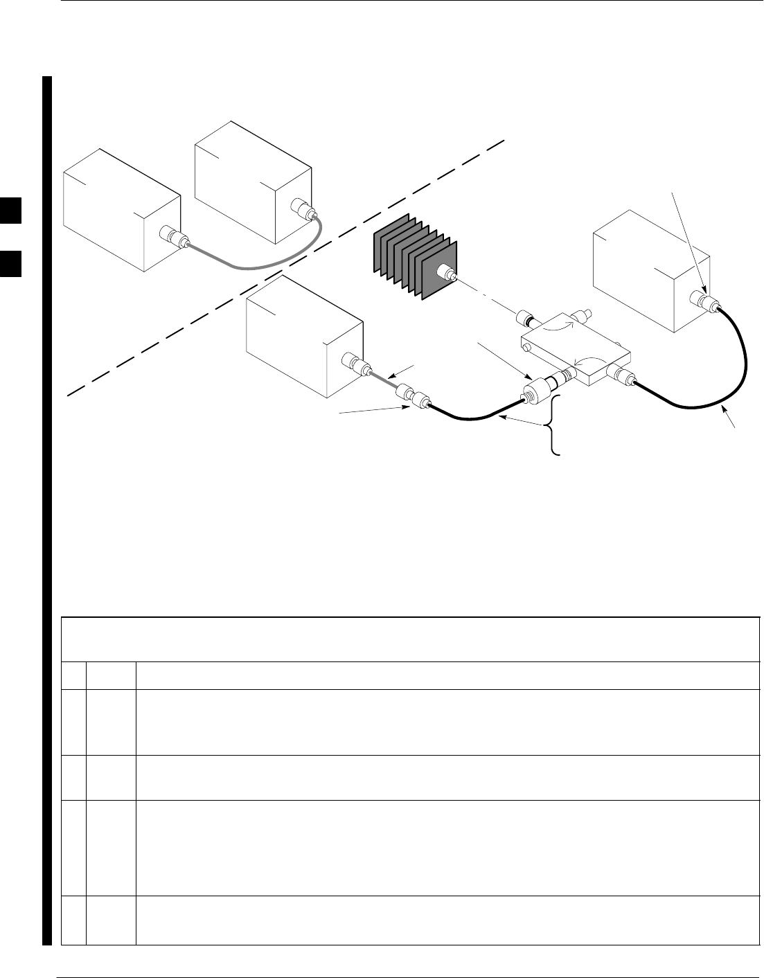
Test Set Calibration – continued
3-108 1X SC 4812T Lite BTS Optimization/ATP FEB 2005
PRELIMINARY
50 OHM
TERMINATOR
30 DB
DIRECTIONAL
COUPLER
Spectrum
Analyzer
Signal
Generator
A
Spectrum
Analyzer
40W NON–RADIATING
RF LOAD
B
SHORT TEST CABLE
Signal
Generator
THIS WILL CONNECT TO THE POWER METER OR
COMMUNICATIONS SYSTEM ANALYZER DURING TX
CALIBRATION AND TO THE COMMUNICATIONS
SYSTEM ANALYZER DURING TX AND RX ATP TESTS.
SHORT
TEST
CABLE
SECOND TX TEST CABLE
FOR TX CAL AND ATP
20DB 20 W IN–LINE
ATTENUATOR FOR
1.9 GHZ
THIS WILL CONNECT TO THE BTS TX
ANTENNA CONNECTOR DURING TX
CALIBRATION AND TO THE TX/RX ANTENNA
CONNECTORS DURING ATP TESTS.
TX TEST
CABLE
RX TEST CABLE
FOR RX ATP TEST
OR
Figure 3-42: Calibration Set–up for TX/Duplexed RX Test Cabling
using a Signal Generator and a Spectrum Analyzer
Non-Duplexed RX Cable Calibration
Table 3-34: Non–Duplexed RX Test Cabling Using Signal Generator and Spectrum Analyzer
Calibration Procedure
nStep Action
* IMPORTANT
When preparing to calibrate a BTS with Duplexed TX and RX, the RX Cable Calibration must be
done using the Calibration Set–up in Figure 3-42 and the procedure in Table 3-33.
1Connect a Short Test Cable between the Spectrum Analyzer and the Signal Generator as shown in
Figure 3-43, Detail “A” (top portion of figure).
2Set the Signal Generator to –10 dBm at the Customer’s RX Frequency.
– 824.7–848.31 MHz for North American Cellular
or
– 1850–1910 MHz for North American PCS
3Use the Spectrum Analyzer to measure Signal Generator Output.
– Record the value for the Detail “A” Set–up.
table continued on next page
3
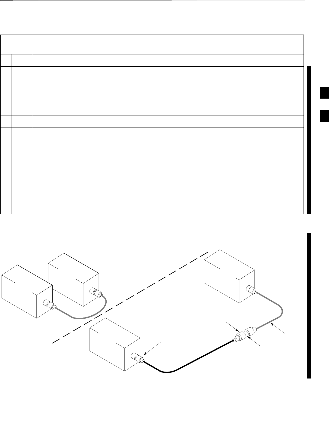
Test Set Calibration – continued
FEB 2005 1X SC 4812T Lite BTS Optimization/ATP 3-109
PRELIMINARY
Table 3-34: Non–Duplexed RX Test Cabling Using Signal Generator and Spectrum Analyzer
Calibration Procedure
nActionStep
4Change the Test Set–up to the one shown in Detail “B” (lower portion of Figure 3-43) to measure
the output at the Customer’s RX Frequency.
– 824.7–848.31 MHz for North American Cellular
or
– 1850–1910 MHz for North American PCS
5Record the value measured with the Detail “B” Test Set–up.
6Calibration Factor = (Value measured with Detail “A” Set–up) – (Value measured with Detail “B”
Set–up)
Example: Calibration Factor = –12 dBm – (–14 dBm) = 2 dB
* IMPORTANT
The Short Test Cable is used for Test Equipment Set–up Calibration Only.
– It is not part of the Final Test Set–up.
After Calibration is completed, do not re-arrange any cables.
– Use the Test Cable Configuration as–is to ensure Test Procedures use the correct Calibration
Factor.
Spectrum
Analyzer
Signal
Generator
A
B
Spectrum
Analyzer
SHORT
TEST
CABLE
CONNECTION TO THE COMMUNICATIONS
SYSTEM ANALYZER RF OUTPUT
CONNECTOR DURING RX MEASUREMENTS
Signal
Generator
BULLET
CONNECTOR
TX
Test
Cable
SHORT TEST
CABLE
CONNECTION TO THE BTS RX ANTENNA
CONNECTOR DURING RX ATP
IMPORTANT: IF BTS TX/RX SIGNALS ARE
DUPLEXED, THE RX TEST CABLE CONNECTS
TO THE DUPLEXED ANTENNA CONNECTOR
AND MUST USE/BE CALIBRATED WITH THE 30
DB DIRECTIONAL COUPLER AND 20 DB
IN–LINE ATTENUATOR. SEE FIGURE 3-42.
Figure 3-43: Calibration Set–up for Non–Duplexed RX Test Cabling
using a Signal Generator and a Spectrum Analyzer
3
Test Set Calibration – continued
3-110 1X SC 4812T Lite BTS Optimization/ATP FEB 2005
PRELIMINARY
Setting Cable Loss Values Cable Loss Values for TX and RX Test Cable Configurations are
normally set by accomplishing Automatic Cable Calibration using the
LMF and the applicable Test Equipment. The LMF stores the measured
Signal Loss Values in the Test Cable Insertion Loss Files. The Test
Cable Insertion Loss Values can also be set or changed manually.
If Cable Calibration was performed without using the
LMF, Test Cable Insertion Loss Values must be manually
entered in the LMF Database. Failure to do this will result
in inaccurate BTS Calibration and reduced site
performance.
CAUTION
Prerequisites
SLMF is logged into the BTS.
Table 3-35: Setting Cable Loss Values Procedure
nStep Action
1 Click Util in the BTS Menu Bar, and select Edit > Cable Loss in the Pull–down Menus.
–A Tabbed Data Entry Pop–up Window will appear.
2Click on the TX Cable Loss Tab or the RX Cable Loss Tab, as required.
3To add a new Channel Number, perform the following actions.
3a Click on the Add Row Button.
3b Click in the Channel # or Loss (dBm) Column, as required.
3c Enter the desired value.
4To edit existing values, click in the Data Box to be changed and change the value.
5To delete a row, click on the row and then click on the Delete Row Button.
6For each tab that needs to be changed, click on the Save Button to save the displayed values.
7Click on the Dismiss Button to close the window.
* IMPORTANT
SValues entered or changed after the Save Button was used will be lost when the window is
dismissed.
SIf Test Cable Insertion Loss Values exist for two different channels, the LMF will interpolate for
all other channels.
SEntered values will be used by the LMF as soon as they are saved.
SIt is not necessary to log out and log back into the LMF for changes to take effect.
3

Test Set Calibration – continued
FEB 2005 1X SC 4812T Lite BTS Optimization/ATP 3-111
PRELIMINARY
Setting TX Coupler Loss Value If an in–service TX Coupler is installed, the Coupler Loss must be
manually entered so it will be included in the LMF TX Calibration and
Audit Calculations.
Prerequisites
SLMF is logged into the BTS.
SPath Loss, in dB, of the TX Coupler must be known.
Table 3-36: Setting TX Coupler Loss Values Procedure
nStep Action
1 Click Util in the BTS Menu Bar, and select Edit > Coupler Loss... in the Pull–down Menus.
–A Tabbed Data Entry Pop–up Window will appear.
2Click on the TX Coupler Loss Tab or the RX Coupler Loss Tab, as required.
3Click in the Loss (dBm) Column for each carrier that has a coupler and enter the appropriate
value.
4Perform the following actions to edit existing values.
4a Click in the Data Box to be changed.
4b Change the value.
5For each tab that needs to be changed, click on the Save Button to save displayed values.
6Click on the Dismiss Button to close the window.
* IMPORTANT
SValues entered or changed after the Save Button is used will be lost when the window is
dismissed.
SThe In–Service Calibration Check Box in the Tools > Options > BTS Options Tab must be
checked before entered TX Coupler Loss Values will be used by the TX Calibration and Audit
Functions.
SNew or changed values will be used by the LMF as soon as they are saved.
SLogging out and logging in again are not required to cause saved changes to take effect.
3

Bay Level Offset Calibration
3-112 1X SC 4812T Lite BTS Optimization/ATP FEB 2005
PRELIMINARY
Introduction
Bay Level Offset (BLO) Calibration is the central activity of the
Optimization Process. BLO Calibration compensates for normal
equipment variations within the BTS RF Paths and assures that the
correct Transmit Power is available at the BTS Antenna Connectors to
meet site performance requirements.
What is BLO Calibration?
Description
BLO Calibration is the complete title of what is normally referred to as
“Calibration.” Calibration identifies the accumulated Gain in every
Transmit Path at the BTS Site.
The Transmit Path BLO Values determined during Calibration are stored
in the LMF Calibration Data File, and are subsequently downloaded to
each BBX. When Transmit Path Calibration is performed, Receive Path
BLO Values are automatically set to the Default Value in the LMF
Calibration File and downloaded.
BTS RF Path Descriptions
Transmit (TX) Path
A TX Path starts at an SCCP Cage BBX Backplane Slot, travels
through the CIO Card, is routed to the Power Amplifier (PA) Trunking
Module for Sector Phase Shifting, through the PAs, back through the PA
Trunking Module for Sector Phase Selection, through the TX Bandpass
Filter (Starter Frames) or 2:1 TX Combiner (Expansion Frames),
through the Transmit and Receive Filter (TRF) or Duplexer TX/RF Filter
(DRF), and ends at the TRF or DRF Antenna Connector..
Receive (RX) Main Path
A Main RX Path starts at ANTENNAS Connectors 1A, 2A, or 3A and
travels through the associated TRF or DRF, the MPC in the SCCP Cage
MPC–1 Slot, the CIO Card, and terminates at a Backplane BBX Slot in
the SCCP Cage..
Diversity RX Path
Diversity RX Paths differ for SC4812T Lite Starter and Expansion
Frames. The following describe each type of path.:
SStarter Frame Diversity RX Path – A Starter Frame Diversity RX
Path is the same as a Main RX Path except that it starts at
ANTENNAS Connectors 1B, 2B, or 3B, travels through the
associated TRF or DRF, and the MPC Card in SCCP Cage MPC–2
Slot.
3

Bay Level Offset Calibration – continued
FEB 2005 1X SC 4812T Lite BTS Optimization/ATP 3-113
PRELIMINARY
SExpansion Frame Diversity RX Path – The Starter Frame Main RX
Signal is used for the Expansion Frame Diversity RX Signal. An
Expansion Frame’s Diversity RX Path starts at ANTENNAS
Connectors 1A, 2A, or 3A in the Starter Frame. It travels through the
associated TRF or DRF, the MPC in SCCP Cage MPC–1 Slot, and the
CIO Card where it is then routed out of the frame through the RX
Expansion Out Connectors (RX EXPANSION 1A, 2A, or 3A).
The signal travels through the Inter–frame Diversity RX Cables, into
the RX Expansion In Ports (RX EXPANSION 1B, 2B, or 3B) of the
Expansion Frame, through the Expansion MPC (EMPC) in SCCP
Cage MPC–2 Slot, the CIO, and terminates at a Backplane BBX Slot
in the SCCP Cage.
SRFDS sampling paths – Directional Couplers for RFDS signal
sampling are integral to the SC4812T Lite Transmit and Receive Paths
in the DRFs and TRFs. Cables connect from these Directional
Couplers to the RFDS Input Connectors.
Component Verification During
Calibration
TX Path Calibration
TX Path Calibration supports verification of correct BTS installation, RF
Cabling installation and performance, functionality of all equipment
installed in the Transmit RF Chain, and the proper functioning of each
Transmit RF Path. External Test Equipment is used to calibrate and audit
the TX Paths of the BTS.
RX Path Calibration
RX Path Calibration is not required or supported on CDMA BTS
systems. Default RX Calibration Values are written to the RX
Calibration Data Files during the TX Calibration process. RX
Functionality is verified during Frame Erasure Rate (FER) Testing.
When to Calibrate BLOs
Calibration to determine BLO:
1. Is required after Initial BTS Installation.
2. Must be done once each year for an operational BTS Site.
3. Is recommended by Motorola for all associated RF Paths after
replacing any of the following components.
– BBX Card
– SCCP Cage
– CIO Card
– CIO–to–PA Trunking Module RF Cable
– PA Trunking Module
– Power Amplifier
– Trunking Module–to–TX Filter/Filter Combiner RF Cable
3

Bay Level Offset Calibration – continued
3-114 1X SC 4812T Lite BTS Optimization/ATP FEB 2005
PRELIMINARY
– TX Filter or TX Filter Combiner
– TX Filter/Filter Combiner–to–DRF/TRF Cable
– DRF or TRF
BLO Calibration Data File
During the Calibration Process, the LMF creates a Calibration (CAL)
Data File where BLO Values are stored. After Calibration has been
completed, these Offset Values must be downloaded to the BBX Cards
using the LMF BLO Download Function. A detailed description of the
file organization and content is provided in the following paragraphs.
Due to the size of the file, Motorola recommends printing
out a copy of a bts–#.cal file and referring to it for the
following descriptions.
NOTE
CAL File Organization
The CAL File is subdivided into three sections called “Slot Blocks”.
These are:
1. Slot[1] Block that contains the Calibration Data for the six Primary
BBX Slots.
2. Slot[20] Block that contains the Calibration Data for the Redundant
BBX. Refer to Table 3-38.
3. Slot[385] Block that contains the Calibration Data for the RFDS.
BBX Slot Block Parts
BBX Slot Blocks are further subdivided into the parts described in the
following paragraphs.
Slot Block Header – Each BBX Slot Block has a Header Section (Slot
Header) that contains the following items.:
SA Creation Date and Time – broken down into separate parameters of
“createMonth”, “createDay”, “createYear”, “createHour”, and
“createMin”.
SThe number of Calibration Entries in the file – the
“numBayLevelPts” Parameter. The parameter is fixed at 720 entries
for SC4812 Series Frames. These 720 entries are combined to define
the 360 Calibration Points of the CAL File.
SThe slot Block format parameter.
Slot Block Bay Level Calibration Data – Each BBX Slot Block has a
Bay Level Calibration Data Section (BayLevelCal) that is organized as a
large flat array. The array is organized by Branch, SCCP Cage BBX
Slot, and Calibration Entries.
There are several ways to look at the array contents. Two different views
are provided in the following to illustrate the significant features of
“BayLevelCal” section content and organization:
3
Bay Level Offset Calibration – continued
FEB 2005 1X SC 4812T Lite BTS Optimization/ATP 3-115
PRELIMINARY
SThe first view of the array is shown in Table 3-37. This view shows
the three branches of the array (Transmit, Main Receive, and
Diversity Receive Offsets, and the Calibration Entry ranges that apply
to each.
Table 3-37: BLO bts–#.cal File Array Branch Assignments
Range Branch Assignment
C[1]–C[120] Transmit
C[121]–C[240] No SC4812T Lite BLO Cal Point Entries (Default only)
C[241]–C[360] Receive
C[361]–C[480] No SC4812T Lite BLO Cal Point Entries (Default only)
C[481]–C[600] Diversity Receive
C[601]–C[720] No SC4812T Lite BLO Cal Point Entries (Default only)
SThe second view of the array is shown in Table 3-38. This view shows
the assignment of Calibration Entries in each branch to each BBX
Slot, Carrier, and Sectorization. Three sectors are allowed in an
SC4812T Lite BTS Frame.
Table 3-38: SC4812T Lite bts–#.cal File Array (by BBX/Sector)
BBX Sectorization TX Branch RX Branch RX Diversity
Branch
Slot[1] (Primary BBX Cards 1 through 6)
1 (Omni) C[1]–C[20] C[241]–C[260] C[481]–C[500]
23–Sector,
1st Carrier C[21]–C[40] C[261]–C[280] C[501]–C[520]
3
1st Carrier
C[41]–C[60] C[281]–C[300] C[521]–C[540]
4 C[61]–C[80] C[301]–C[320] C[541]–C[560]
53–Sector,
2n
d Ca
rri
e
rC[81]–C[100] C[321]–C[340] C[561]–C[580]
6
2nd Carrier
C[101]–C[120] C[341]–C[360] C[581]–C[600]
C[121]–C[140] C[361]–C[380] C[601]–C[620]
C[141]–C[160] C[381]–C[400] C[621]–C[640]
Not Used in SC4812T Lite
(CAL File Entries are Channel 0 with
C[161]–C[180] C[401]–C[420] C[641]–C[660]
(CAL Fil
e
E
ntr
i
es
are
Ch
anne
l 0
w
i
t
h
Default Power Set Level) C[181]–C[200] C[421]–C[440] C[661]–C[680]
)
C[201]–C[220] C[441]–C[460] C[681]–C[700]
C[221]–C[240] C[461]–C[480] C[701]–C[720]
table continued next page
3
Bay Level Offset Calibration – continued
3-116 1X SC 4812T Lite BTS Optimization/ATP FEB 2005
PRELIMINARY
Table 3-38: SC4812T Lite bts–#.cal File Array (by BBX/Sector)
BBX RX Diversity
Branch
RX BranchTX BranchSectorization
Slot[20] (Redundant BBX–R1)
1 (Omni) C[1]–C[20] C[241]–C[260] C[481]–C[500]
23–Sector,
1
st Ca
rri
e
rC[21]–C[40] C[261]–C[280] C[501]–C[520]
3
1st Carrier
C[41]–C[60] C[281]–C[300] C[521]–C[540]
4 C[61]–C[80] C[301]–C[320] C[541]–C[560]
53–Sector,
2n
d Ca
rri
e
rC[81]–C[100] C[321]–C[340] C[561]–C[580]
6
2nd Carrier
C[101]–C[120] C[341]–C[360] C[581]–C[600]
C[121]–C[140] C[361]–C[380] C[601]–C[620]
C[141]–C[160] C[381]–C[400] C[621]–C[640]
Not Used in SC4812T Lite
(CAL File Entries are Channel 0 with
C[161]–C[180] C[401]–C[420] C[641]–C[660]
(CAL Fil
e
E
ntr
i
es
are
Ch
anne
l 0
w
i
t
h
Default Power Set Level) C[181]–C[200] C[421]–C[440] C[661]–C[680]
)
C[201]–C[220] C[441]–C[460] C[681]–C[700]
C[221]–C[240] C[461]–C[480] C[701]–C[720]
SWhen referring to the CAL File Printout and Table 3-38, it can be seen
that there is one BBX Slot per sector with 20 “Calibration Entries” per
BBX (sector) for each branch. Two Calibration Entries define a single
“Calibration Point;” therefore there are ten Calibration Points in each
branch for each BBX.
– The first Calibration Entry for a Calibration Point (all odd entries)
identifies the CDMA Channel (frequency) where the BLO is
measured.
– The second Calibration Entry (all even entries) is the Power Set
Level (PwrLvlAdj) for that frequency. The valid range for
“PwrLvlAdj” is from 2500 to 27500 (2500 corresponds to
–125 dBm and 27500 corresponds to +125 dBm).
– The ten Calibration Points for each Slot–Branch Combination must
be stored in order of increasing frequency. If less than ten points
(frequencies) are calibrated, the BLO Data for the highest frequency
calibrated is written into the remainder of the ten points for that
Slot–Branch.
3

Bay Level Offset Calibration – continued
FEB 2005 1X SC 4812T Lite BTS Optimization/ATP 3-117
PRELIMINARY
Example:
C[1]=384 (Odd Cal Entry)
C[2]=19102 (Even Cal Entry)
C[3]=777 (Odd Cal Entry)
C[4]=19086 (Even Cal Entry)
C[19]=777 (Odd Cal Entry)
C[20]=19086 (Even Cal Entry)
.
.
.
= 1 “Calibration Point”
= 1 “Calibration Point”
= 1 “Calibration Point”
In the example above, BLO was measured at only two frequencies
(Channels 384 and 777) for SCCP BBX–1 Slot Transmit (Table 3-38).
The BLO Data for the highest frequency measured (Channel 777) will
be written to the remaining eight Transmit Calibration Points (defined
by Entry C[5] through Entry C[20]) for BBX–1.
Slot Block Temperature Compensation – Each BBX Slot Block also
has a Temperature Compensation Data Section (TempLevelCal) where
Power Level Compensation Factors for Temperature Variations are
stored..
CAL File and BLO Data Download
When BLO Data is downloaded to the BBX Cards after Calibration, the
data is downloaded to the devices in the order it is stored in the CAL
File. TX Calibration Data (Entries C[1] through C[60]) are sent first.
Data for the ten BBX Slot 1 Calibration Points (Entries C[1] through
C[20]) are sent initially, followed by data for the ten BBX Slot 2
Calibration Points (Entries C[21] through C[40]), and so on. The RX
Calibration Data is sent next in BBX Slot Sequence, followed by the RX
Diversity Calibration Data.
Test Equipment Set–up for
RF Path Calibration
Perform the procedure in Table 3-39 and refer as needed to Figure 3-16
or Figure 3-17 to Set–up Test Equipment.
Table 3-39: Set–up Test Equipment for RF Path Calibration Procedure
nStep Action
1If it has not already been done, refer to the procedure in Table 3-6 (on Page 3-18) to interface the
LMF Computer Terminal to the BTS Frame LAN A Connector.
2If it has not already been done, refer to Table 3-10 (on Page 3-29) to start a GUI LMF Session.
3If required, calibrate the Test Equipment per the procedure in Table 1-4.
table continued on next page
3

Bay Level Offset Calibration – continued
3-118 1X SC 4812T Lite BTS Optimization/ATP FEB 2005
PRELIMINARY
Table 3-39: Set–up Test Equipment for RF Path Calibration Procedure
nActionStep
! CAUTION
To prevent damage to the Test Equipment, all Transmit (TX) Test Connections must be via the 30
dB Directional Coupler for 800 MHz or via a 30 dB Coupler with a 20 dB In–line Attenuator for
1900 MHz.
4For TX Path Calibration, connect the Test Equipment as shown in Figure 3-16, Figure 3-17, or
Figure 3-18, depending on the Communications Analyzer being used.
Transmit (TX) Path Calibration
Description
The assigned Channel Frequency and desired Power Level at the Frame
TX Ports for transmit Calibration are derived from the BTS CDF File.
Each BBX at the site is assigned to a Sector and Carrier. These are
specified respectively in the Sector and Carrier Fields of the
“ParentCARRIER“ Parameter in each BBX Cards CDF File Block.
The Channel Frequency and desired Power Output for the assigned
sector are specified respectively in the “ChannelList“ and
“SIFPilotPwr“ Parameters of the CDF Block for the CARRIER to
which the BBX is assigned.
Ensure that the bts–#.cdf (or bts–#.necf) and cbsc–#.cdf
Files loaded on the LMF Computer are current. The LMF
will obtain carrier and channel information from these
files and insert it into the appropriate CDMA Test
Parameter Screen.
Failure to have the most current files from the CBSC can
result in incorrect channel information being used to
calibrate the BTS and unfavorable affects on BTS
performance.
Carrier and Channel Numbers should only be entered
manually for special test cases or as a last resort.
NOTE
The Calibration Process attempts to adjust the measured Power Output
to within +0.5 dB of the desired Power Output. The Calibration Settings
will pass if the error is less than +1.5 dB.
The TX BLO for the SC 4812T Lite is approximately 45.0 dB +5.0 dB.
BLO is the Gain in dB between the known Power Output of the BBX
and the measured Power Input at the TX Port. BLO is derived by
deducting the known BBX Power Output from the Power Input
measured at the TX Port or (Measured TX Port Power Input) – (BBX
TX Power Output).
3

Bay Level Offset Calibration – continued
FEB 2005 1X SC 4812T Lite BTS Optimization/ATP 3-119
PRELIMINARY
Example:
Measured Power Input (at TX Port) = 39.0 dBm
Known BBX TX Power Output = –6.0 dBm
BLO = (39.0) – (–6.0) = 45.0 dB Gain
TX Calibration and the LMF
The LMF Tests > TX > TX Calibration... and Tests > All Cal/Audit...
Selections perform TX BLO Calibration Testing for installed BBX(s).
– The All Cal/Audit... Selection initiates a series of actions to
perform TX Calibration, and if Calibration is successful, download
BLO and perform TX Audit.
– The TX Calibration... Selection performs only TX Calibration.
When TX Calibration... is used, BLO Download and TX Audit
must be performed as separate activities. The CDMA Test
Parameters Window that opens when TX Calibration... or All
Cal/Audit... is selected contains several “user–selectable” Features
that are described in the following subsections.
Rate Set Drop–down Pick List
The Rate Set Drop–down Box is enabled if at least one MCC Card is
selected for the test. The available options for TX Tests are 1 = 9600,
and 3 = 9600 1X.
– Option 2 is only available if no 1X Cards are selected.
– Option 3 is only available if 1X Cards are selected for the test.
– The available Transfer Rate Options for RX Tests are 1 = 9600 and
2 = 14400.
Verify BLO Check Box
In both the TX Calibration and All Cal/Audit Dialog Boxes, a Verify
BLO Check Box is provided and checked by default. After the actual
TX Calibration is completed during either the TX Calibration or All
Cal/Audit Process, the BLO derived from the Calibration is compared to
a standard acceptable BLO Tolerance for the BTS.
In some installations, additional items may be installed in the Transmit
Path. The additional change in Gain from these items could cause BLO
Verification Failure and, therefore, failure of the entire Calibration.
– In these cases, either the Verify BLO Check Box should be
unchecked or the additional Path Losses should be added into each
applicable sector using the Util>Edit>TX Coupler Loss...
Function.
Single–Sided BLO Check Box
An acceptable range of BLO Values for each type of BTS is established
to allow for tolerance variations in all the components of the RF Chain.
This acceptable range, 45.0 +5 dB for example, is very wide to
accommodate the Redundant BBX in the BTS. This is a much wider
tolerance than necessary for the Primary BBX Cards.
3
Bay Level Offset Calibration – continued
3-120 1X SC 4812T Lite BTS Optimization/ATP FEB 2005
PRELIMINARY
Primary BBX Cards normally will have BLOs in the lower half of the
range. Using the example range, this would be from 40 to 45 dB.
Checking the Single–Sided BLO Check Box should only be done when
calibrating Primary BBX Cards because it will reduce the acceptable
BLO Value variations to the lower half of the range. Because this is a
much more stringent tolerance, Calibrations run with Single–Sided
BLO are more likely to fail and should only be attempted by an
experienced CFE.
Never select Single–Sided BLO when calibrating a
Redundant BBX.
IMPORTANT
*
Test Pattern Drop–down Pick List
The Tests > TX > TX Calibration... Menu Window has a Test Pattern
Pull–down Menu. This menu has the following choices:
SStandard – performs Calibration or Audit using Pilot, Paging, Synch,
and six Traffic Channels with IS–97–specified Gain. This Pattern
Setting should be used for all non–In–service Calibrations and Audits.
Using this Pattern Setting requires the selection of one
BBX and at least one MCC.
IMPORTANT
*
SPilot (Default) – performs Calibration using only the Pilot Channel.
This Pattern Setting should be used for In–service
Calibrations, and requires selection of only one BBX.
IMPORTANT
*
SCDFPilot – This Pattern Setting is for advanced users. It performs
Calibration or Audit using the CDF Value for Pilot Gain and IS–97
Gain Values for all the other channels included in the Standard
Pattern Setting (Paging, Synch, and six Traffic).
Using this Pattern Setting requires the selection of one
BBX and at least one MCC.
IMPORTANT
*
SCDF – This Pattern Setting is for advanced users who need to use
CDF Gain Settings for all channels included in the Standard Pattern
Setting (Pilot, Paging, Synch, and six Traffic).
Using this Pattern Setting requires the selection of one
BBX and at least one MCC.
IMPORTANT
*
3
Bay Level Offset Calibration – continued
FEB 2005 1X SC 4812T Lite BTS Optimization/ATP 3-121
PRELIMINARY
Test Pattern Channels and Gain Settings – The CDMA Channels and
their respective Digital Gain Settings used for each Test Pattern are listed
in Table 3-40.
Table 3-40: Test Patterns with Channels and Gain Settings Used
Test Pattern Channel(s) Gain Setting
Pilot Pilot Channel only 541
Standard Pilot 117
Synch Channel
(SCH) 57
Paging (PCH) 114
Traffic (TCH) 80 for each of 6 Walsh Codes
used (6*80)
CDF Pilot Pilot Uses CDF–specified Pilot Gain
SCH 57
PCH 114
TCH 6*80
CDF Pilot All channels use
CDF ifi d G i
SCH CDF–specified Gains
PCH
TCH (6)
TX Calibration
Before installing any Test Equipment directly to any BTS
TX OUT Connector, first verify that no CDMA
Channels are keyed.
– Failure to do so can result in serious personal injury
and/or equipment damage.
WARNING
Always wear an approved Anti–static Wrist Strap while
handling any Circuit Card or Module.
– If this is not done, there is a high probability that the
card or module could be damaged by ESD.
CAUTION
3

Bay Level Offset Calibration – continued
3-122 1X SC 4812T Lite BTS Optimization/ATP FEB 2005
PRELIMINARY
At new site installations, to facilitate the complete test of
each SCCP Cage (if the cage is not already fully populated
with BBX Cards), move BBX Cards from shelves
currently not under test and install them into the empty
BBX Slots of the shelf currently being tested to insure that
all BBX TX Paths are tested.
– This procedure can be bypassed on operational sites
that are due for periodic Optimization.
– Prior to testing, view the CDF (or NECF) File to
verify that the correct BBX Slots are equipped. Edit
the file as required to include BBX Slots not currently
equipped (per Systems Engineering Documentation).
NOTE
All Cal/Audit and TX
Calibration Procedure
The LMF All Cal/Audit and TX Calibration Procedures are essentially
identical, except for the step that selects the type of procedure desired.
– Refer to Step 4 in Table 3-41.
Prerequisites
Before running this procedure, make sure that the following
actions/items have been performed/checked.
SThe CSM Card in the CSM 1 Slot, GLI Cards, MCC Cards, and BBX
Cards have correct Code and Data Loads.
SThe LEDs on the Primary CSM and MGLI Cards are INS_ACTIVE
(bright green).
SAll BBX Cards are OOS_RAM (yellow).
SIf running Calibration or Audit using a Test Pattern other than Pilot,
MCC Cards are INS_ACTIVE (bright green).
STest Equipment and Test Cables are calibrated and connected for TX
Calibration.
SThe LMF is logged into the BTS in the GUI Environment.
Verify that all BBX Cards removed and repositioned have
been returned to their assigned shelves/slots.
Any BBX Cards that were moved since they were
downloaded need to be downloaded again.
NOTE
Perform the procedure in Table 3-41 to perform BLO Calibration on the
TX Paths, download BLO Values to the BBX Cards, and perform TX
Path Audit in one operation.
3

Bay Level Offset Calibration – continued
FEB 2005 1X SC 4812T Lite BTS Optimization/ATP 3-123
PRELIMINARY
Table 3-41: All Cal/Audit and TX Calibration Procedure
nStep Action
1If it has not already been done, configure the Test Equipment for TX Calibration by performing
the procedure in Table 3-39.
2Click on the BBX(s) to be calibrated.
3If the Test Pattern to be used is Standard, CDFPilot, or CDF, select at least one MCC.
– Refer to “Test Pattern Drop–down Pick List” under “TX Calibration and the LMF” in this
section.
4For All Cal Audit...
Click Tests in the BTS Menu Bar, and select TX > All Cal/Audit... from the Pull–down Menus.
– A CDMA Test Parameters Window will appear.
For TX Calibration
Click Tests in the BTS Menu Bar, and select TX > TX Calibration from the Pull–down Menus.
– A CDMA Test Parameters Window will appear.
5Select the appropriate carrier(s) and sector(s) (carrier-bts#-sector#-carrier#) from those displayed
in the Channels/Carrier Pick List.
NOTE
To select multiple items, hold down the Shift or Ctrl Key while clicking on Pick List Items to
select multiple carrier(s)–sector(s).
6Verify that the correct Channel Number for the selected carrier is shown in the Carrier #
Channels Box.
SIf it is not, obtain the latest bts–#.cdf (or bts–#.necf) and cbsc–#.CDF Files from the CBSC.
NOTE
If necessary, the correct Channel Number may be manually entered into the Carrier # Channels
Box.
7If at least one MCC was selected in Step 3, select the appropriate Transfer Rate (1 = 9600, 3 =
9600 1X) from the Pull–down Menu in the Rate Set Box.
NOTE
The Rate Selection of 3 is only available if 1X Cards are selected for the test.
8 If Verify BLO is to be used during the Calibration, leave the Check Box checked (default).
9If Single–Sided BLO is to be used during the Calibration, click on the Check Box.
* IMPORTANT
Single–Sided BLO should only be used for Primary BBX Cards.
– Do not check the box when calibrating the Redundant BBX.
table continued on next page
3

Bay Level Offset Calibration – continued
3-124 1X SC 4812T Lite BTS Optimization/ATP FEB 2005
PRELIMINARY
Table 3-41: All Cal/Audit and TX Calibration Procedure
nActionStep
10 In the Test Pattern Box, select the Test Pattern to use for the Calibration from the Pull–down
Menu.
– Refer to “Test Pattern Drop–down Pick List” under “TX Calibration and the LMF” in this
section.
11 Click OK to display the Status Report Window.
–A Directions Pop-up Window will then appear.
12 Follow the Cable Connection Directions as they are displayed.
– When the Calibration Process is completed, results will be displayed in the Status Report
Window.
13 Click OK to close the Status Report Window.
Exception Handling
In the event of a failure, the Calibration Procedure displays a FAIL
message in the Status Report Window and provides information in the
Description Field.
Re–check the Test Set–up and connection and re–run the Calibration. If
the Calibration fails again, note specifics about the failure, and refer to
Chapter 6, Troubleshooting.
Download BLO Procedure
After a successful TX Path Calibration, download the BLO Calibration
File Data to the BBX Cards. BLO Data is extracted from the CAL File
for the BTS and downloaded to the selected BBX Cards.
If a successful All Cal/Audit was completed, this
procedure does not need to be performed, since BLO is
downloaded as part of the All Cal/Audit.
NOTE
Prerequisites
Ensure the following prerequisites have been met before proceeding.
SBBX Cards to receive the download are OOS_RAM (yellow).
STX Calibration was successfully completed.
Perform the procedure in Table 3-42 to download the BLO Data to the
BBX Cards.
3
Bay Level Offset Calibration – continued
FEB 2005 1X SC 4812T Lite BTS Optimization/ATP 3-125
PRELIMINARY
Table 3-42: Download BLO Data Procedure
nStep Action
1Select the BBX(s) to be downloaded.
2 Click Device in the BTS Menu Bar, and select Download > BLO from the Pull–down Menus.
– A Status Report Window displays the result of the download.
NOTE
Selected device(s) do not change color when BLO is downloaded.
3 Click OK to close the Status Report Window.
Calibration Audit Introduction
The BLO Calibration Audit Procedure confirms the successful
generation and storage of the BLO Calibration values. The Calibration
Audit Procedure measures the Path Gain or Loss of every BBX Transmit
Path at the site. In this test, actual system tolerances are used to
determine the success or failure of a test. The same External Test
Equipment Set–up required for TX Calibration is used for TX Audit.
RF Path Verification, BLO Calibration, and BLO Data
Download to BBX Cards must be successfully completed
prior to performing the Calibration Audit.
NOTE
TX Path Audit
Perform the Calibration Audit of the TX Paths of all equipped BBX
Slots, per the steps in Table 3-43.
If a successful All Cal/Audit was completed, this
procedure does not need to be performed, as BLO is
downloaded as part of the All Cal/Audit.
NOTE
Before installing any Test Equipment directly to any TX
OUT Connector, first verify that there are no CDMA
BBX channels keyed.
Failure to do so can result in serious personal injury
and/or equipment damage.
WARNING
3

Bay Level Offset Calibration – continued
3-126 1X SC 4812T Lite BTS Optimization/ATP FEB 2005
PRELIMINARY
TX Audit Test
The Tests Menu Item, TX Audit, performs the TX BLO Audit Test for
BBX Cards. All measurements are made through the appropriate TX
Output Connector using the TX Calibration Set–up.
Prerequisites
Before running this test, the following should be done:
SThe CSM 1 Card, GLI Cards, and BBX Cards all have the correct
Code Load.
SThe Primary CSM and MGLI Cards are INS_ACTIVE (bright green).
SAll BBX Cards are OOS_RAM (yellow).
SThe Test Equipment and Test Cables are calibrated and connected for
TX BLO Calibration.
SThe LMF is logged into the BTS.
TX Path Audit Procedure
After a TX Calibration has been performed, or if verification of BLO
Data in the CAL File is required, perform the procedure in Table 3-43 to
perform a BTS TX Path Audit.
Table 3-43: BTS TX Path Audit Procedure
nStep Action
1If it has not already been done, configure Test Equipment for TX Path Audit by performing the
procedure in Table 3-39.
NOTE
TX Audit uses the same configuration as TX Calibration.
2Select the BBX(s) to be audited.
3If the Test Pattern to be used is Standard, CDFPilot, or CDF, select at least one MCC.
– Refer to “Test Pattern Drop–down Pick List” under “TX Calibraton and the LMF” in this
section.
4 Click Tests in the BTS Menu Bar, and select TX > TX Audit... from the Pull–down Menus.
– A CDMA Test Parameters Window will appear.
5Select the appropriate carrier(s) (carrier-bts#-sector#-carrier#) from those displayed in the
Channels/Carrier Pick List.
NOTE
To select multiple items, hold down the Shift or Ctrl Key while clicking on Pick List Items to
select multiple carrier(s)–sector(s).
table continued on next page
3

Bay Level Offset Calibration – continued
FEB 2005 1X SC 4812T Lite BTS Optimization/ATP 3-127
PRELIMINARY
Table 3-43: BTS TX Path Audit Procedure
nActionStep
6Verify that the correct Channel Number for the selected carrier is shown in the Carrier #
Channels Box.
SIf it is not, obtain the latest bts–#.cdf (or bts–#.necf) and cbsc–#.CDF Files from the CBSC.
NOTE
If necessary, the correct Channel Number may be manually entered into the Carrier # Channels
Box.
7If at least one MCC was selected in Step 3, select the appropriate Transfer Rate (1 = 9600, 3 =
9600 1X) from the Pull–down Menu in the Rate Set Box.
NOTE
The Rate Selection of 3 is only available if 1X Cards are selected for the test.
8From the Test Pattern Pick List, select a Test Pattern.
– Selecting Pilot (default) performs tests using a Pilot Signal only.
– Selecting Standard performs tests using Pilot, Synch, Paging, and six Traffic Channels. This
requires an MCC to be selected.
– Selecting CDFPilot performs tests using the CDF Value for Pilot Gain and IS–97 Gain Values
for all the other channels included in the Standard Pattern Setting (Paging, Synch, and six
Traffic). Using this Pattern Setting requires the selection of a BBX and at least one MCC.
– Selecting CDF performs tests using Pilot, Synch, Paging and six Traffic Channels. However,
the Gain for the Channel Elements is specified in the CDF File.
9 Click OK to display the Status Report Window followed by a Directions Pop-up Window.
10 Follow the Cable Connection Directions as they are displayed.
– When the Calibration Process is completed, results will be displayed in the Status Report
Window.
11 Click on the Save Results or Dismiss Button, as desired, to close the Status Report Window.
Exception Handling
In the event of a failure, the Calibration Procedure displays a FAIL
Message in the Status Report Window and provides information in the
Description Field.
Re–check the Test Set–up and connections and re–run the test. If the
tests fail again, note specifics about the failure, and refer to Chapter 6,
Troubleshooting.
Create CAL File
The LMF Create Cal File Function gets the BLO Data from BBX Cards
and creates/updates the CAL File for the BTS.
SIf a CAL File does not exist, a new one is created.
SIf a CAL File already exists it is updated.
3
Bay Level Offset Calibration – continued
3-128 1X SC 4812T Lite BTS Optimization/ATP FEB 2005
PRELIMINARY
After a BTS has been fully optimized a copy of the CAL File must be
present so it can be transferred to the CBSC.
SIf TX Calibration has been successfully performed for all BBX Cards
and BLO Data has been downloaded, a CAL File will exist.
The Create Cal File Function only applies to selected
(highlighted) BBX Cards.
NOTE
Editing the CAL File is not encouraged because this
action can cause interface problems between the BTS and
the LMF.
To manually edit the CAL File you must first logout of
the BTS.
– If you manually edit the CAL File and then use the
Create Cal Function, the edited information will be
lost.
CAUTION
Prerequisites
Before running this procedure, the following should be done:
SThe LMF is logged into the BTS.
SThe BBX Cards are OOS_RAM (yellow)
SThe BLO has been downloaded to the BBX Cards.
Table 3-44: Create CAL File Procedure
nStep Action
1Select the applicable BBX Cards.
– The CAL File will be updated for the selected BBX Cards only.
2Click on Device in the BTS Menu Bar, and select Create Cal File from the Pull–down Menu.
– A Status Report Window will appear and display the results of the action.
3Click the OK Button to close the Status Report Window.
3

RFDS Set–up and Calibration
FEB 2005 1X SC 4812T Lite BTS Optimization/ATP 3-129
PRELIMINARY
RFDS Description
The optional RFDS is used to perform RF Tests of the site from the
CBSC or from the LMF. The RFDS contains the following FRUs:
SAntenna Select Unit (ASU)
SFixed Wireless Terminal Interface Card (FWTIC)
SSubscriber Unit Assembly (SUA)
For complete information regarding the RFDS, refer to the CDMA
CDMA RFDS Hardware Installation; 68P64113A93, CDMA RFDS
User’s Guide; 68P64114A51, and the LMF Help function on–line
documentation.
RFDS Parameters
The bts–#.CDF File includes RFDS Parameter Settings that must match
the installed RFDS equipment. The paragraphs below describe the
editable parameters and their defaults. Table 3-45 explains how to edit
the Parameter Settings.
SRfdsEquip – valid inputs are 0 through 2.
0 = (default) RFDS is not equipped
1 = Non-Cobra/Patzer Box RFDS
2 = Cobra RFDS
STsuEquip – valid inputs are 0 or 1
0 = (default) TSU not equipped
1 = TSU is equipped in the system
SMC1....4 – valid inputs are 0 or 1
0 = (default) Not equipped
1 = Multicouplers equipped in RFDS System
(SC9600 internal RFDS only)
SAsu1/2Equip – valid inputs are 0 or 1
0 = (default) Not equipped
1 = Equipped
STestOrigDN – valid inputs are ’’’ (default) or a numerical string up to
15 characters.
– This is the phone number the RFDS dials when originating a call. A
dummy number needs to be set–up by the switch, and is to be used
in this field.
Any Text Editor may be used to open the bts–#.CDF File
to verify, view, or modify data.
Because the bts–#.CDF File is generated on a UNIX
system, a more sophisticated editor, such as MicroSoft
WordPad, will display file content in a more easily–read
format than many simple Text Editors.
NOTE
3

RFDS Set–up and Calibration – continued
3-130 1X SC 4812T Lite BTS Optimization/ATP FEB 2005
PRELIMINARY
Checking and Setting RFDS
Parameters
Perform the procedure in Table 3-45 to review and/or edit RFDS
Parameters.
Table 3-45: RFDS Parameter Settings Procedure
nStep Action
NOTE
Log out of the BTS prior to perform this procedure.
1Using a Text Editor, verify that the following fields are set correctly in the bts–#.cdf File.
EXAMPLE:
Asu1Equip = 1
Asu2Equip = 0 (1 if system is non-duplexed)
Mc1Equip = 0
Mc2Equip = 0
Mc3Equip = 0
Mc4Equip = 0
RfdsEquip = 2
TestOrigDN = ’123456789’
TsuEquip = 1
NOTE
The above is an example of entries extracted from the bts–#.cdf File that should have been
generated by the OMC–R and copied to the LMF.
– These fields will have been set by the OMC–R if the RFDSPARM Database is modified for
the RFDS.
2Save changes and/or quit the editor.
3Log into the BTS using an LMF GUI Session.
– Refer to Table 3-10.
4Determine if changes were made to the bts–#.cdf File Fields listed in Step 1.
SIf changes were not made, proceed to Step 7.
SIf changes were made, proceed to Step 5.
NOTE
To make certain the complete data download is accepted, the MGLI should be OOS_RAM
(yellow) when RFDS Parameter Settings are downloaded.
5When changes are made to RFDS Parameters in the bts–#.CDF File, data must be downloaded to
the MGLI by performing the following actions
5a To be sure it does not take control when the MGLI is disabled, manually disable the Redundant
GLI Card by unseating it from the Backplane Connectors and sliding it partially out of the SCCP
Cage Slot.
5b Click on the MGLI.
table continued on next page
3

RFDS Set–up and Calibration – continued
FEB 2005 1X SC 4812T Lite BTS Optimization/ATP 3-131
PRELIMINARY
Table 3-45: RFDS Parameter Settings Procedure
nActionStep
5c Click on Device in the BTS Menu Bar, and select Disable from the Pull–down Menu.
– A Status Report Window shows the status of the operation.
5d When the operation is complete, click OK to close the Status Report Window.
5e Click on the MGLI [now OOS_RAM (yellow)].
5f Click on Device in the BTS Menu Bar, and select Download > Data from the Pull–down Menus.
– A Status Report Window shows the status of the download.
NOTE
Selected devices do not change color when data is downloaded.
5g Click OK to close the Status Report Window.
5h Click on the MGLI.
5i Click on Device in the BTS Menu Bar, and select Enable from the Pull–down Menu.
– A Status Report Window shows the status of the operation.
5j When the operation is complete, click OK to close the Status Report Window.
! CAUTION
When the MGLI changes to INS_ACTIVE, data will automatically be downloaded to the RFDS.
– During this process, the RFDS LED will slowly begin flashing red and green for
approximately 2–3 minutes.
–DO NOT attempt to perform any functions with the RFDS until the LED remains steady
green.
5k Re–seat the Redundant GLI Card into its Backplane Connector and lock it in place with the
Ejector Tabs.
5l Once the Redundant GLI initializes, download data to it by performing the following actions:
– Select the card.
– Click Device in the BTS Menu Bar.
– Select Download > Data from the Pull–down Menu.
6Any MCC Cards that were INS_ACTIVE when the MGLI was disabled must be disabled,
downloaded with data, and re–enabled as follows:
6a Select the devices to be reset.
– Click on them.
or
– Choose Select from the BTS Menu Bar and click on MCC Cards in the Pull–down Menu.
6b In the BTS Menu Bar, click on Device and select Disable from the Pull–down Menu.
– A Status Report Window shows the status of the operation.
table continued on next page
3

RFDS Set–up and Calibration – continued
3-132 1X SC 4812T Lite BTS Optimization/ATP FEB 2005
PRELIMINARY
Table 3-45: RFDS Parameter Settings Procedure
nActionStep
6c Click OK to close the Status Report Window.
6d Repeat Step 6a to select the MCC Cards.
6e Click on Device in the BTS Menu Bar and select Download > Data from the Pull–down Menu.
– A Status Report Window shows the status of the download.
NOTE
Selected devices do not change color when data is downloaded.
6f Click on OK to close the Status Report Window.
6g When data download is complete, enable the MCC Cards by performing the procedure in
Table 3-21.
7Click on the RFDS Tab.
8Status the RFDS TSU by performing the following actions.
8a Click on the SUA to select it.
8b Click on TSU in the BTS Menu Bar, and select Status TSU from the Pull–down Menu.
– A Status Report shows the software Version Number for the TSIC and SUA.
8c Click OK to close the Status Report Window.
* IMPORTANT
If the LMF Displays an Error Message, check the following:
SEnsure that the AMR Cable from the BTS to the RFDS is connected correctly.
SVerify that the RFDS has power.
SVerify that the RFDS Status LED is green.
SVerify that the entries in the RFDS Fields of the bts–#.CDF File are correct.
– Refer to Step 1.
SStatus the MGLI and ensure it is communicating (by Ethernet) with the LMF, and is in the
proper state [INS_ACTIVE (bright green)].
3

RFDS Set–up and Calibration – continued
FEB 2005 1X SC 4812T Lite BTS Optimization/ATP 3-133
PRELIMINARY
RFDS TSU NAM Programming
The Number Assignment Module (NAM) information needs to be
programmed into the TSU before it can receive and process Test Calls,
or be used for any type of RFDS Test. The RFDS TSU NAM must be
programmed with the appropriate system parameters and a phone
number during hardware installation. The TSU Phone Number and TSU
MSI must be recorded for each BTS used for OMC–R RFDS Software
Configuration.
The user will only need to program the NAM for the initial
installation of the RFDS.
NOTE
Explanation of Parameters
Used When Programming the
TSU NAM
Table 3-46 defines the parameters used when editing the tsu.nam file.
Table 3-46: Definitions of NAM Parameters
Access Overload Code
Slot Index
System ID
Network ID
These parameters are obtained from the switch.
Primary Channel A
Primary Channel B
Secondary Channel A
Secondary Channel B
These parameters are the channels that are to be used in operation of the
system.
Lock Code
Security Code
Service Level
Station Class Mark
Do NOT change.
IMSI MCC
IMSI 11 12 These fields are obtained at the OMC using the following command:
omc–000000 >disp bts–# imsi
If the fields are blank, replace the IMSI Fields in the NAM File to 0,
otherwise use the values displayed by the OMC–R.
MIN Phone Number This field is the phone number assigned to the mobile.
– The ESN and MIN must be entered into the switch as well.
NOTE
This field is different from the TODN Field in the bts–#.CDF File.
– The MIN is the phone number assigned to the RFDS Subscriber.
– The TODN is the phone number that the subscriber calls.
3

RFDS Set–up and Calibration – continued
3-134 1X SC 4812T Lite BTS Optimization/ATP FEB 2005
PRELIMINARY
Valid NAM Ranges
Table 3-47 provides the valid NAM Field Ranges. If any of the fields are
missing or out-of–range, the RFDS will error out.
Table 3-47: Valid NAM Field Ranges
Valid Range
NAM Field Name Minimum Maximum
Access Overload Code 0 15
Slot Index 0 7
System ID 0 32767
Network ID 0 32767
Primary Channel A 25 1175
Primary Channel B 25 1175
Secondary Channel A 25 1175
Secondary Channel B 25 1175
Lock Code 0 999
Security Code 0 999999
Service Level N/A N/A
Station Class Mark 0 255
IMSI 11 12 0 99
IMSI MCC 0 999
MIN Phone Number N/A N/A
3

RFDS Set–up and Calibration – continued
FEB 2005 1X SC 4812T Lite BTS Optimization/ATP 3-135
PRELIMINARY
Set Antenna Map Data
The Antenna Map Data must be entered manually if an RFDS is
installed. Antenna Map Data does not need to be entered if an RFDS is
not installed. The Antenna Map Data is only used for RFDS Tests and is
required if an RFDS is installed.
Prerequisite
SThe LMF is logged into the BTS.
Perform the procedure in Table 3-48 to set Antenna Map Data for the
RFDS.
Table 3-48: Set Antenna Map Data Procedure
nStep Action
1Click on Util in the BTS Menu Bar, and select Edit > Antenna Map... from the Pull–down Menu.
– A tabbed Data Entry Pop–up Window will appear.
2In the Data Entry Pop–up Window, click on the TX Antenna Map or RX Antenna Map Tab to
select the Antenna Map to be edited.
3Locate the Carrier and Sector Number for which data is to be entered or edited, and click in the
column where entry or editing is needed.
4 Enter/edit Antenna # and Antenna Label column data as needed for each carrier.
NOTE
Refer to the CDMA Help > Utility Menu > Edit–Antenna Map... section of LMF Help function
on–line documentation for Antenna Map examples.
5For each Tab that needs to be changed, click on the Save Button to save displayed values.
6Click on the Dismiss Button to close the window.
NOTE
SValues entered or changed after the Save Button was used will be lost when the window is
dismissed.
– Entered values will be used by the LMF as soon as they are saved.
SIt is not necessary to log out and log back into the LMF for changes to take effect.
3

RFDS Set–up and Calibration – continued
3-136 1X SC 4812T Lite BTS Optimization/ATP FEB 2005
PRELIMINARY
Set RFDS Configuration Data
If an RFDS is installed, the RFDS Configuration Data must be manually
entered.
Prerequisite
SLMF is logged into the BTS
The entered antenna# index numbers must correspond to
the antenna# index numbers used in the Antenna Maps.
NOTE
Perform the procedure in Table 3-49 to set RFDS Configuration Data.
Table 3-49: Set RFDS Configuration Data Procedure
nStep Action
1Click on Util in the BTS Menu Bar, and select Edit > RFDS Configuration... from the
Pull–down Menus.
–A Tabbed Data Entry Pop–up Window will appear.
2In the Data Entry Pop–up Window, click on the TX RFDS Configuration or RX RFDS
Configuration Tab, as required.
3To add a new Antenna Number, perform the following actions.
3a Click on the Add Row Button.
3b Click in the Antenna #, Cal Antenna, Scap Antenna, or Populate [Y/N] Columns, as required.
3c Enter the desired data.
4To edit existing values click in the Data Box to be changed and change the value.
NOTE
Refer to the CDMA Help > Utility Menu > Edit–RFDS Configuration... section of LMF Help
function on–line documentation for RFDS Configuration Data examples.
5To delete a row, click on the row and then click on the Delete Row Button.
6For each tab that needs to be changed, click on the Save Button to save the displayed values.
7Click on the Dismiss Button to close the window.
NOTE
SValues entered or changed after the Save Button was used will be lost when the window is
dismissed.
– Entered values will be used by the LMF as soon as they are saved.
SIt is not necessary to log out and log back into the LMF for changes to take effect.
3
RFDS Set–up and Calibration – continued
FEB 2005 1X SC 4812T Lite BTS Optimization/ATP 3-137
PRELIMINARY
RFDS Calibration
The RFDS Calibration option is used to calibrate the RFDS TX and RX
Paths.
TX Path Calibration
For a TX Antenna Path Calibration, the BTS XCVR is keyed at a
pre–determined Power Level and the BTS Power Output Level is
measured by the RFDS. The Power Level is then measured at the TX
Antenna Directional Coupler by the power measuring Test Equipment
Item being used (Power Meter or Analyzer).
– The difference (Offset) between the Power Level at the RFDS and
the Power Level at the TX Antenna Directional Coupler is used as
the TX RFDS Calibration Offset Value.
RX Path Calibration
For an RX Antenna Path Calibration, the RFDS is keyed at a
pre–determined Power Level and the Power Input Level is measured by
the BTS BBX. A CDMA signal at the same Power Level measured by
the BTS BBX is then injected at the RX antenna Directional Coupler by
the Communications System Analyzer.
– The difference (Offset) between the RFDS–keyed Power Level and
the Power Level measured at the BTS BBX is the RFDS RX
Calibration Offset Value.
RFDS Calibration and the CAL File
The TX and RX RFDS Calibration Offset Values are written to the CAL
File in the Slot[385] Block.
TSIC Channel Frequency
For each RFDS TSIC, the Channel Frequency is determined at the
lower third and upper third of the appropriate band using the frequencies
listed in Table 3-50..
Table 3-50: RFDS TSIC Calibration Channel Frequencies
System Channel Calibration Points
800 MHz (A and B) 341 and 682
1.9 GHz 408 and 791
Before installing any Test Equipment directly to any TX
OUT Connector, verify that there are no CDMA
Channels keyed.
– Failure to do so can result in serious personal injury
and/or equipment damage.
WARNING
3

RFDS Set–up and Calibration – continued
3-138 1X SC 4812T Lite BTS Optimization/ATP FEB 2005
PRELIMINARY
Prerequisites
STest Equipment has been selected.
STest Equipment and Test Cables have been calibrated.
STX Calibration has been performed and BLO Data has been
downloaded to the BBX Cards.
STest Equipment and Test Cables are connected for TX Calibration.
SAntenna Map Data has been entered for the site.
SBBX Cards are OOS–RAM.
RFDS Calibration Procedure
Perform the procedure in Table 3-51 to perform RFDS Calibration.
Table 3-51: RFDS Calibration Procedure
nStep Action
1In the LMF, select the CDMA BTS–xxx Tab.
2If the BTS Control Button is not selected (no black dot showing), click on the B Button in the BTS
Menu Bar to select it.
3Select the BBX(s) assigned to the carrier(s) and sector(s) that will be used in RFDS Calibration.
– Refer to Table 1-5 for BBX Carrier and Sector Assignments).
4Click on RFDS in the BTS Menu Bar, and select RFDS Calibration... from the Pull–down
Menu.
– An RFDS Calibration Set–up window will be displayed.
5In the Tests to Perform Box, select TX Calibration or RX Calibration, as required
6Enter the appropriate Channel Number(s) in the Channel Field Box.
– Refer to Table 3-50.
STo enter more than one Channel Number, use the following methods, as needed.
– Separate non–sequential Channel Numbers with a comma and no spaces;
for example: 247,585,742.
– Enter a range of sequential Channel Numbers by typing the first and last Channel Numbers in
the range separated by a dash and no spaces;
for example: 385–395.
7If the frame is equipped with TX Combiners, click in the Has Combiners Check Box.
8Select the appropriate carrier(s) and sector(s) from the Carriers Pick List.
NOTE
Hold down the Shift or Ctrl Key while clicking on Pick List Items to select multiple
carrier(s)–sector(s).
9If performing RX Calibration,.select the appropriate RX Branch (Both, Main, or Diversity) in the
Pull–down Menu.
table continued on next page
3
RFDS Set–up and Calibration – continued
FEB 2005 1X SC 4812T Lite BTS Optimization/ATP 3-139
PRELIMINARY
Table 3-51: RFDS Calibration Procedure
nActionStep
10 Click on the OK Button.
– A Status Report Window is displayed, followed by a Directions Pop–up Window.
11 Follow the Cable Connection Directions as they are displayed.
12 When the test is completed, the test results are displayed in the Status Report Window.
13 Click on the OK Button to close the Status Report Window.
14 Click on the BTS Frame Tab.
15 Select the MGLI by clicking on it.
16 Download updated RFDS offset data to the MGLI.
– Refer to Step 5 in Table 3-45.
TSU Program TSU NAM
The NAM must be programmed before it can receive and process Test
Calls, or be used for any type of RFDS Test.
Prerequisites
SMGLI is INS_ACTIVE (bright green).
SSUA is powered up and has a Code Load.
Perform the procedure in Table 3-52 to program the TSU NAM.
Table 3-52: Program TSU NAM Procedure
nStep Action
1In the LMF, select the RFDS Tab.
2Select the SUA by clicking on it.
3Click on TSU in the BTS Menu Bar, and select Program TSU NAM from the Pull–down Menu.
– A NAM programming window will appear.
4Enter the appropriate information in the boxes. Refer to Table 3-46 and Table 3-47) .
5Click on the OK Button to display the Status Report.
6Click on the OK Button to close the Status Report Window.
3
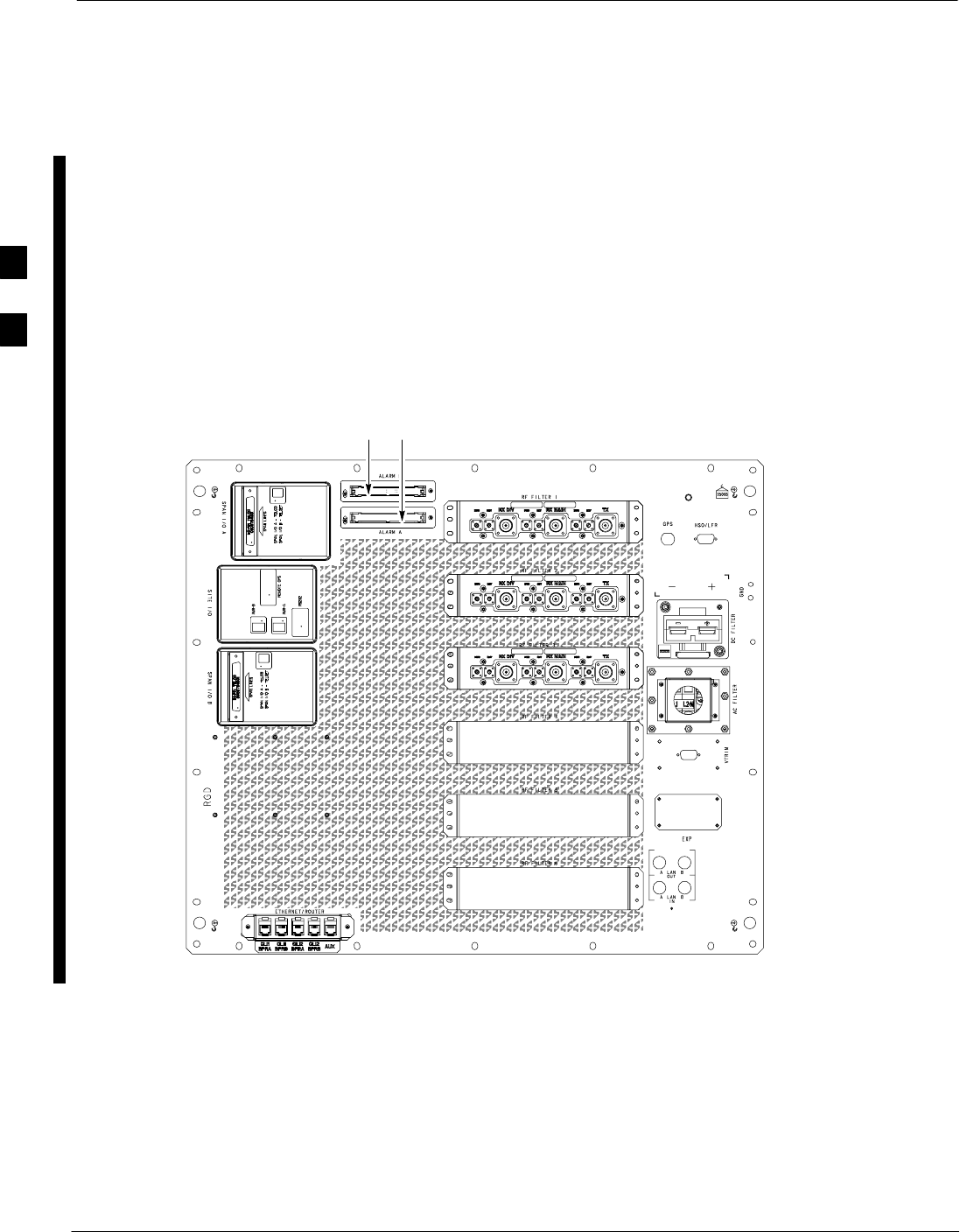
Alarms Testing
3-140 1X SC 4812T Lite BTS Optimization/ATP FEB 2005
PRELIMINARY
Alarm Verification
ALARM Connectors provide Customer Defined Alarm Inputs and
Outputs. The customer can connect BTS Site Alarm Input Sensors and
Output Devices to the BTS, thus providing Alarm Reporting from active
sensors as well as controlling Output Devices.
The SC 4812T Lite is capable of concurrently monitoring 35 Iinput
Signals. These Input Signals are divided between two Alarm Connectors
marked ‘ALARM A’ and ‘ALARM B’ located at the top of the frame.
Refer to Figure 3-44.
FRONT
REAR
ti-CDMA-WP-00233-v01-ildoc-ftwREF
ALARM CONNECTORS
BA
Figure 3-44: Alarm Connector Location and Connector Pin Numbering
3
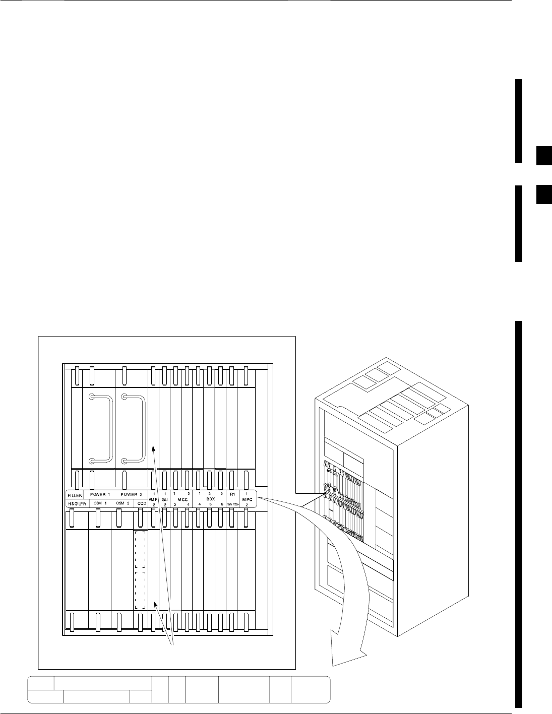
Alarms Testing – continued
FEB 2005 1X SC 4812T Lite BTS Optimization/ATP 3-141
PRELIMINARY
Alarm A and Alarm B Connector Comparison
The ALARM A Connector is always functional; the ALARM B
Connector is functional when an AMR Card is equipped in the AMR 2
Slot in the SCCP Cage. Refer to Figure 3-45.
The ALARM A Port monitors Input Numbers 1 through 9 and 11
through 18, while ALARM B Port monitors Input Numbers 19 through
36. Refer to Figure 3-46.
– Alarm 10 is reserved for system use.
– State Transitions on these Input Lines are reported to the LMF and
OMC–R as MGLI Input Relay Alarms.
ALARM A and ALARM B Connectors each provide 18 Inputs and 8
Outputs.
– If both A and B are functional, 36 Inputs and 16 Outputs are
available.
– They may be configured as redundant.
– The configuration is set by the CBSC.
ti-CDMA-WP-00222-v01-ildoc-ftw REF
MPC/EMPC
CSM
Power Supply
Power Supply
MPC/EMPC
CSM
CCD–1CCD–2
AMR 2
HSO
AMR 1
GLI GLI
MCC
MCC
MCC
MCC
BBX
BBX
BBX
BBX
BBX
BBX
SWITCH
19mm Filler Panel
BBX
CIO
AMR CARDS
SCCP CAGE
FILLER POWER 1 POWER 2
HSO/LFR CSM 1 CSM 2 CCD AMR GLI
1 2
3 4
MCC
1 2 3
4 5 6
BBX R1
SWITCH
1
2
1
2
1
2
MPC
Figure 3-45: SCCP Cage
3
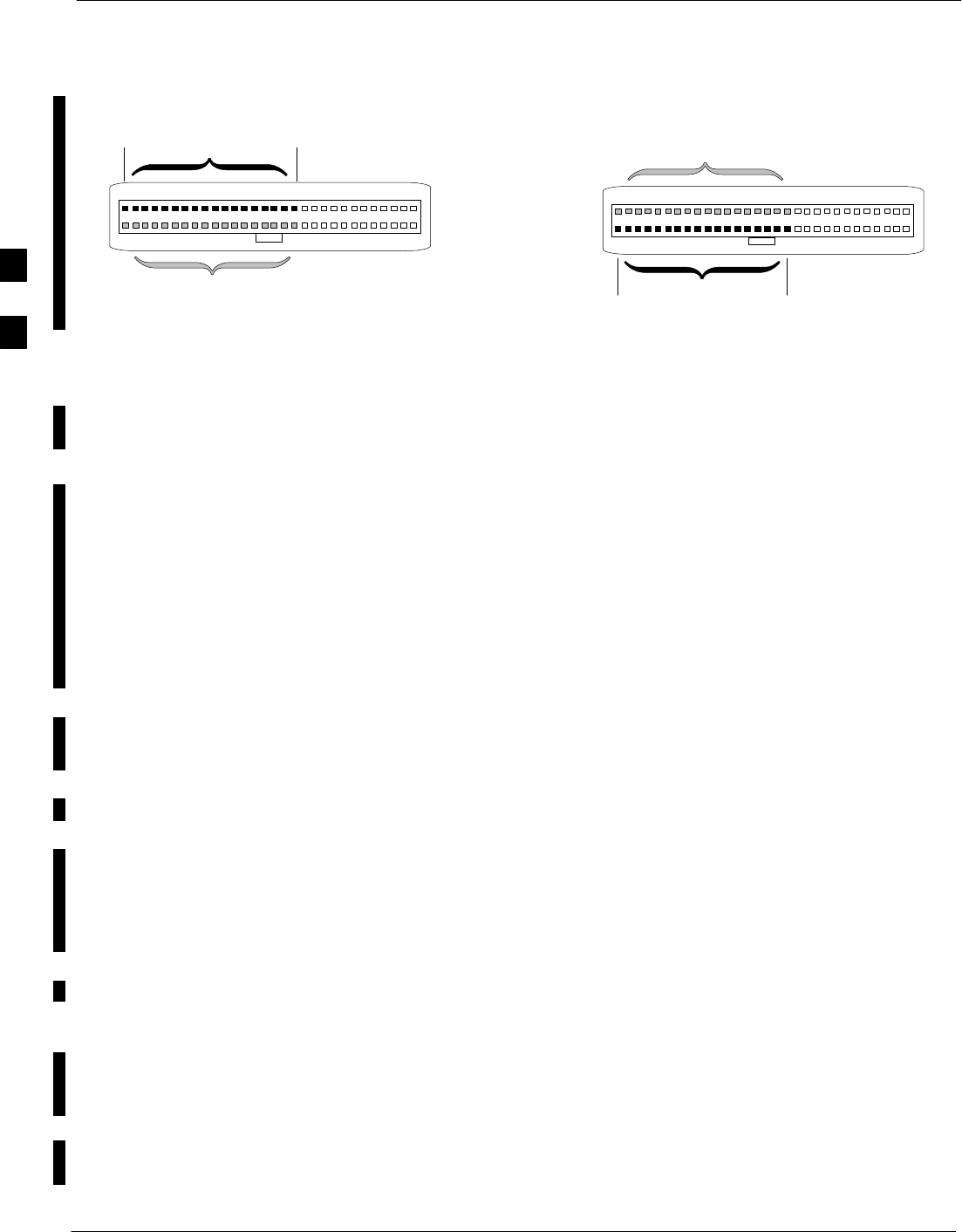
Alarms Testing – continued
3-142 1X SC 4812T Lite BTS Optimization/ATP FEB 2005
PRELIMINARY
59 1
60 2
ALARM A
(AMR 1) ALARM B
(AMR 2)
Returns
25
26
A CDI 18 . . . A CDI 1
59 1
60 2
Returns
25
26
B CDI 36 . . . B CDI 19 FW00302
Figure 3-46: AMR Connector Pin Numbering
Alarm Reporting Display
The Alarm Monitor Window can be displayed to list alarms that occur
after the window is displayed. To access the Alarm Monitor Window,
select Util>Alarm Monitor.
The following buttons are included:
SThe Options Button allows for a Severity Level (Warning, Minor,
and Major) Selection.
– The default is ALL LEVELS.
– To change the level of alarms reported, click on the Options Button
and highlight the desired Alarm Level(s).
– To select multiple levels press the <Ctrl> Key (for individual
selections) or <Shift> Key (for a range of selections) while clicking
on the desired levels.
SThe Pause Button pauses/stops the display of alarms.
– When the Pause Button is clicked the name of the button changes
to Continue.
– When the Continue Button is clicked, the display of alarms
continues.
– Alarms that occur between the time the Pause Button is clicked and
the Continue Button is clicked are not displayed.
SThe Clear Button clears the Alarm Monitor Display.
– New alarms that occur after the Clear Button is clicked are
displayed.
SThe Dismiss Button dismisses/closes the Alarm Monitor Display.
Purpose The following procedures verify that the Customer–defined Alarms and
Relay Contacts are functioning properly. These tests are performed on all
AMR Alarms/Relays in a sequential manner until all have been verified.
Perform these procedures periodically to ensure the External Alarms are
reported properly. Performing these procedures ensures continued peak
system performance.
3

Alarms Testing – continued
FEB 2005 1X SC 4812T Lite BTS Optimization/ATP 3-143
PRELIMINARY
Study the Site Engineering Documents and perform the following tests
only after first verifying that the AMR Cabling Configuration required
to interconnect the BTS Frame with External Alarm Sensors and/or
Relays meet requirements stated in the 1X SC4812T Lite Hardware
Installation manual (68P09262A57) Manual.
Motorola highly recommends that before you start this
procedure, you read and understand it in its entirety.
NOTE
Test Equipment
The following Test Equipment is required to perform these tests:
SLMF
SAlarms Test Box (CGDSCMIS00014) –optional
Abbreviations used in the following figures and tables are
defined as:
SNC = Normally Closed
SNO = Normally Open
SCOM or C = Common
SCDO = Customer Defined (Relay) Output
SCDI = Customer Defined (Alarm) Input
NOTE
The preferred method to verify alarms is to follow the
Alarms Test Box Procedure in Table 3-53. If not using an
Alarm Test Box, perform the procedure in Table 3-54.
NOTE
CDI Alarm Input Verification
with Alarms Test Box
Table 3-53 describes how to test the CDI Alarm Input verification using
the Alarm Test Box. Follow the steps as instructed and compare results
with the LMF Display.
It may take a few seconds for alarms to be reported. The
default delay is 5 seconds.
Leave the Alarms Test Box switches in the new position
until the alarms have been reported.
NOTE
3

Alarms Testing – continued
3-144 1X SC 4812T Lite BTS Optimization/ATP FEB 2005
PRELIMINARY
Table 3-53: CDI Alarm Input Verification Procedure (using the Alarms Test Box)
nStep Action
1Connect the LMF to the BTS.
2Log into the BTS.
3Select the MGLI.
4Click on the Device Menu.
5Click on the Set Alarm Relays Menu Item.
6Click on Normally Open.
– A Status Report Window displays the results of the action.
7Click on the OK Button to close the Status Report Window.
8Set all switches on the Alarms Test Box to the Open position.
NOTE
Input 10 (Pins 43 and 44) on the Alarm A Connector is reserved for the Power Supply Modules
Alarm.
9Connect the Alarms Test Box to the ALARM A Connector.
– Refer to Figure 3-44.
10 Set all of the switches on the Alarms Test Box to the Closed position.
– An alarm should be reported for each Backplane Configuration Switch Setting.
11 Set all of the switches on the Alarms Test Box to the Open position.
– An Alarm Clear Message should be reported for each Backplane Configuration Switch Setting.
12 Disconnect the Alarms Test Box from the ALARM A Connector.
13 Connect the Alarms Test Box to the ALARM B Connector.
14 Set all switches on the Alarms Test Box to the Closed position.
– An alarm should be reported for each Backplane Configuration Switch Setting.
15 Set all switches on the Alarms Test Box to the Open position.
– An Alarm Clear Message should be reported for each Backplane Configuration Switch Setting.
16 Disconnect the Alarms Test Box from the ALARM B Connector.
17 Select the MGLI.
18 Click on the Device Menu.
19 Click on the Set Alarm Relays Menu Item.
20 Click on Normally Closed.
– A Status Report Window displays the results of the action.
table continued on next page
3

Alarms Testing – continued
FEB 2005 1X SC 4812T Lite BTS Optimization/ATP 3-145
PRELIMINARY
Table 3-53: CDI Alarm Input Verification Procedure (using the Alarms Test Box)
nActionStep
21 Click OK to close the Status Report Window.
– Alarms should be reported for Alarm Inputs 1 through 36.
22 Set all switches on the Alarms Test Box to the Closed position.
23 Connect the Alarms Test Box to the ALARM A Connector.
– Alarms should be reported for Alarm Inputs 1 through 18.
24 Set all switches on the Alarms Test Box to the Open position.
– An alarm should be reported for each Backplane Configuration Switch Setting.
25 Set all switches on the Alarms Test Box to the Closed position.
– An Alarm Clear Message should be reported for each Backplane Configuration Switch Setting.
26 Disconnect the Alarms Test Box from the ALARM A Connector.
27 Connect the Alarms Test Box to the ALARM B Connector.
– An Alarm Clear Message should be reported for Alarm Inputs 19 through 36.
28 Set all switches on the Alarms Test Box to the Open position.
– An alarm should be reported for each Backplane Configuration Switch Setting.
29 Set all switches on the Alarms Test Box to the Closed position.
– An Alarm Clear Message should be reported for each Backplane Configuration Switch Setting.
30 Disconnect the Alarms Test Box from the ALARM B Connector.
31 Select the MGLI.
32 Click on the Device Menu.
33 Click on the Set Alarm Relays Menu Item.
34 Click on Unequipped.
– A Status Report Window displays the results of the action.
35 Click on the OK Button to close the Status Report Window.
36 Connect the Alarms Test Box to the ALARM A Connector.
37 Set all switches on the Alarms Test Box to both the Open and the Closed position.
– No alarm should be reported for any Backplane Configuration Switch Settings.
38 Disconnect the Alarms Test Box from the ALARM A Connector.
39 Connect the Alarms Test Box to the ALARM B Connector.
40 Set all switches on the Alarms Test Box to both the Open and the Closed position.
– No alarm should be reported for any Backplane Configuration Switch Settings.
table continued on next page
3

Alarms Testing – continued
3-146 1X SC 4812T Lite BTS Optimization/ATP FEB 2005
PRELIMINARY
Table 3-53: CDI Alarm Input Verification Procedure (using the Alarms Test Box)
nActionStep
41 Disconnect the Alarms Test Box from the ALARM B Connector.
42 Load data to the MGLI to reset the Alarm Relay Conditions according to the CDF File.
CDI Alarm Input Verification
without Alarms Test Box
Table 3-54 describes how to test the CDI Alarm Input verification
without the use of the Alarms Test Box. Follow the steps as instructed
and compare results with the LMF Display.
It may take a few seconds for alarms to be reported. The
default delay is 5 seconds. When shorting Alarm Pins wait
for the Alarm Report before removing the short.
NOTE
Table 3-54: CDI Alarm Input Verification Procedure (without the Alarms Test Box)
nStep Action
1Connect the LMF to the BTS.
2Log into the BTS.
3Select the MGLI.
4Click on the Device Menu.
5Click on the Set Alarm Relays Menu Item.
6Click on Normally Open.
– A Status Report Window displays the results of the action.
7Click on OK to close the Status Report Window.
NOTE
Input 10 (Pins 43 and 44) on the Alarm A Connector is reserved for the Power Supply Modules
Alarm.
8Refer to Figure 3-46 and sequentially short the ALARM A Connector CDI 1 through CDI 18 Pins
(25–26 through 59–60) together.
– An alarm should be reported for each pair of pins that are shorted.
– An Alarm Clear Message should be reported for each pair of pins when the short is removed.
table continued on next page
3

Alarms Testing – continued
FEB 2005 1X SC 4812T Lite BTS Optimization/ATP 3-147
PRELIMINARY
Table 3-54: CDI Alarm Input Verification Procedure (without the Alarms Test Box)
nActionStep
9Refer to Figure 3-46 and sequentially short the ALARM B Connector CDI 19 through CDI 36
pins (25–26 through 59–60) together.
– An alarm should be reported for each pair of pins that are shorted.
– An Alarm Clear Message should be reported for each pair of pins when the short is removed.
10 Select the MGLI.
11 Click on the Device Menu.
12 Click on the Set Alarm Relays Menu Item.
13 Click on Normally Closed.
– A Status Report Window displays the results of the action.
14 Click on OK to close the Status Report Window.
– Alarms should be reported for Alarm Inputs 1 through 36.
NOTE
Input 10 (Pins 43 and 44) on Alarm A Connector is reserved for the Power Supply Modules
Alarm.
15 Refer to Figure 3-46 and sequentially short the ALARM A Connector CDI 1 through CDI 18 Pins
(25–26 through 59–60) together.
– An Alarm Clear Message should be reported for each pair of pins that are shorted.
– An alarm should be reported for each pair of pins when the short is removed.
16 Refer to Figure 3-46 and sequentially short the ALARM B Connector CDI 19 through CDI 36
pins (25–26 through 59–60) together.
– An Alarm Clear Message should be reported for each pair of pins that are shorted.
– An alarm should be reported for each pair of pins when the short is removed.
17 Select the MGLI.
18 Click on the Device Menu.
19 Click on the Set Alarm Relays Menu Item.
20 Click on Unequipped.
– A Status Report Window displays the results of the action.
21 Click on OK to close the Status Report Window.
NOTE
Input 10 (Pins 43 and 44) on Alarm A Connector is reserved for the Power Supply Modules
Alarm.
22 Refer to Figure 3-46 and sequentially short the ALARM A Connector CDI 1 through CDI 18 Pins
(25–26 through 59–60) together.
– No alarms should be displayed.
table continued on next page
3

Alarms Testing – continued
3-148 1X SC 4812T Lite BTS Optimization/ATP FEB 2005
PRELIMINARY
Table 3-54: CDI Alarm Input Verification Procedure (without the Alarms Test Box)
nActionStep
23 Refer to Figure 3-46 and sequentially short the ALARM B Connector CDI 19 through CDI 36
pins (25–26 through 59–60) together.
– No alarms should be displayed.
24 Load data to the MGLI to reset the Alarm Relay Conditions according to the CDF File.
Pin and Signal Information for
Alarm Connectors
Table 3-55 lists the Pins and Signal Names for Alarms A and B.
Table 3-55: Pin and Signal Information for Alarm Connectors
ALARM A ALARM B
Pin Signal Name Pin Signal Name Pin Signal Name Pin Signal Name
1A CDO1 NC 31 Cust Retn 4 1B CDO9 NC 31 B CDI 22
2A CDO1 Com 32 A CDI 4 2B CDO9 Com 32 Cust Retn 22
3A CDO1 NO 33 Cust Retn 5 3B CDO9 NO 33 B CDI 23
4A CDO2 NC 34 A CDI 5 4B CDO10 NC 34 Cust Retn 23
5A CDO2 Com 35 Cust Retn 6 5B CDO10 Com 35 B CDI 24
6A CDO2 NO 36 A CDI 6 6B CDO10 NO 36 Cust Retn 24
7A CDO3 NC 37 Cust Retn 7 7B CDO11 NC 37 B CDI 25
8A CDO3 Com 38 A CDI 7 8B CDO11 Com 38 Cust Retn 25
9A CDO3 NO 39 Cust Retn 8 9B CDO11 NO 39 B CDI 26
10 A CDO4 NC 40 A CDI 8 10 B CDO12 NC 40 Cust Retn 26
11 A CDO4 Com 41 Cust Retn 9 11 B CDO12 Com 41 B CDI 27
12 A CDO4 NO 42 A CDI 9 12 B CDO12 NO 42 Cust Retn 27
13 A CDO5 NC 43 Power Supply
Modules Alarm
Return
13 B CDO13 NC 43 B CDI 28
14 A CDO5 Com 44 Power Supply
Modules Alarm 14 B CDO13 Com 44 Cust Retn 28
15 A CDO5 NO 45 Cust Retn 11 15 B CDO13 NO 45 B CDI 29
16 A CDO6 NC 46 A CDI 11 16 B CDO14 NC 46 Cust Retn 29
17 A CDO6 Com 47 Cust Retn 12 17 B CDO14 Com 47 B CDI 30
18 A CDO6 NO 48 A CDI 12 18 B CDO14 NO 48 Cust Retn 30
table continued next page
3

Alarms Testing – continued
FEB 2005 1X SC 4812T Lite BTS Optimization/ATP 3-149
PRELIMINARY
Table 3-55: Pin and Signal Information for Alarm Connectors
ALARM A ALARM B
Pin Signal NamePinSignal NamePinSignal NamePinSignal Name
19 A CDO7 NC 49 Cust Retn 13 19 B CDO15 NC 49 B CDI 31
20 A CDO7 Com 50 A CDI 13 20 B CDO15 Com 50 Cust Retn 31
21 A CDO7 NO 51 Cust Retn 14 21 B CDO15 NO 51 B CDI 32
22 A CDO8 NC 52 A CDI 14 22 B CDO16 NC 52 Cust Retn 32
23 A CDO8 Com 53 Cust Retn 15 23 B CDO16 Com 53 B CDI 33
24 A CDO8 NO 54 A CDI 15 24 B CDO16 NO 54 Cust Retn 33
25 Cust Retn 1 55 Cust Retn 16 25 B CDI 19 55 B CDI 34
26 A CDI 1 56 A CDI 16 26 Cust Retn 19 56 Cust Retn 34
27 Cust Retn 2 57 Cust Retn 17 27 B CDI 20 57 B CDI 35
28 A CDI 2 58 A CDI 17 28 Cust Retn 20 58 Cust Retn 35
29 Cust Retn 3 59 Cust Retn 18 29 Cust Retn 10 59 B CDI 36
30 A CDI 3 60 A CDI 18 30 A CDI 10 60 Cust Retn 36
NOTE
CDO = Customer Defined Output; CDI = Customer Defined Input
3

Alarms Testing – continued
3-150 1X SC 4812T Lite BTS Optimization/ATP FEB 2005
PRELIMINARY
Notes
3