Nokia Solutions and Networks T6FE1 PCS Licensed Transmitter User Manual 68P09262A58 C
Nokia Solutions and Networks PCS Licensed Transmitter 68P09262A58 C
Contents
- 1. User Manual 1 of 3
- 2. User Manual 2 of 3
- 3. User Manual 3 of 3
User Manual 3 of 3

FEB 2005 1X SC 4812T Lite BTS Optimization/ATP
PRELIMINARY
Chapter 4: Acceptance Test Procedures
Table of Contents
Automated Acceptance Test Procedure 4-1 . . . . . . . . . . . . . . . . . . . . . . . . . . . . . . .
Introduction 4-1 . . . . . . . . . . . . . . . . . . . . . . . . . . . . . . . . . . . . . . . . . . . . . .
Reduced ATP 4-1 . . . . . . . . . . . . . . . . . . . . . . . . . . . . . . . . . . . . . . . . . . . . .
ATP Test Options 4-2 . . . . . . . . . . . . . . . . . . . . . . . . . . . . . . . . . . . . . . . . . .
ATP Prerequisites 4-2 . . . . . . . . . . . . . . . . . . . . . . . . . . . . . . . . . . . . . . . . . .
TX/RX Antenna Connections 4-3 . . . . . . . . . . . . . . . . . . . . . . . . . . . . . . . .
Acceptance Tests – Test Set–up 4-4 . . . . . . . . . . . . . . . . . . . . . . . . . . . . . . . . . . . . .
Required Test Equipment 4-4 . . . . . . . . . . . . . . . . . . . . . . . . . . . . . . . . . . .
Acceptance Test Equipment Set–up 4-4 . . . . . . . . . . . . . . . . . . . . . . . . . . .
Abbreviated (All–inclusive) Acceptance Tests 4-6 . . . . . . . . . . . . . . . . . . . . . . . . . .
All–inclusive Tests 4-6 . . . . . . . . . . . . . . . . . . . . . . . . . . . . . . . . . . . . . . . . .
All TX/RX ATP Test 4-6 . . . . . . . . . . . . . . . . . . . . . . . . . . . . . . . . . . . . . . .
All TX ATP Test 4-8 . . . . . . . . . . . . . . . . . . . . . . . . . . . . . . . . . . . . . . . . . .
All RX ATP Test 4-9 . . . . . . . . . . . . . . . . . . . . . . . . . . . . . . . . . . . . . . . . . .
Individual Acceptance Tests 4-11 . . . . . . . . . . . . . . . . . . . . . . . . . . . . . . . . . . . . . . . .
RX and TX Testing 4-11 . . . . . . . . . . . . . . . . . . . . . . . . . . . . . . . . . . . . . . . .
Individual Tests 4-11 . . . . . . . . . . . . . . . . . . . . . . . . . . . . . . . . . . . . . . . . . . .
TX Spectral Purity Transmit Mask Acceptance Test 4-13 . . . . . . . . . . . . . . . . . . . . .
Background 4-13 . . . . . . . . . . . . . . . . . . . . . . . . . . . . . . . . . . . . . . . . . . . . . .
Spectral Purity TX Mask Acceptance Test 4-14 . . . . . . . . . . . . . . . . . . . . . .
TX Waveform Quality (Rho) Acceptance Test 4-16 . . . . . . . . . . . . . . . . . . . . . . . . . .
Background 4-16 . . . . . . . . . . . . . . . . . . . . . . . . . . . . . . . . . . . . . . . . . . . . . .
Waveform Quality (Rho) Acceptance Test 4-16 . . . . . . . . . . . . . . . . . . . . . .
TX Pilot Time Offset Acceptance Test 4-18 . . . . . . . . . . . . . . . . . . . . . . . . . . . . . . . .
Background 4-18 . . . . . . . . . . . . . . . . . . . . . . . . . . . . . . . . . . . . . . . . . . . . . .
Pilot Time Offset Acceptance Test 4-18 . . . . . . . . . . . . . . . . . . . . . . . . . . . .
TX Code Domain Power/Noise Floor Acceptance Test 4-20 . . . . . . . . . . . . . . . . . . .
Background 4-20 . . . . . . . . . . . . . . . . . . . . . . . . . . . . . . . . . . . . . . . . . . . . . .
Code Domain Power/Noise Floor Test 4-21 . . . . . . . . . . . . . . . . . . . . . . . . .
RX FER Acceptance Test 4-23 . . . . . . . . . . . . . . . . . . . . . . . . . . . . . . . . . . . . . . . . . .
Background 4-23 . . . . . . . . . . . . . . . . . . . . . . . . . . . . . . . . . . . . . . . . . . . . . .
FER Acceptance Test 4-23 . . . . . . . . . . . . . . . . . . . . . . . . . . . . . . . . . . . . . . .
Generating an ATP Report 4-25 . . . . . . . . . . . . . . . . . . . . . . . . . . . . . . . . . . . . . . . . .
Background 4-25 . . . . . . . . . . . . . . . . . . . . . . . . . . . . . . . . . . . . . . . . . . . . . .
ATP Report 4-25 . . . . . . . . . . . . . . . . . . . . . . . . . . . . . . . . . . . . . . . . . . . . . .
4

Table of Contents – continued
1X SC 4812T Lite BTS Optimization/ATP FEB 2005
PRELIMINARY
Updating Calibration Data Files 4-26 . . . . . . . . . . . . . . . . . . . . . . . . . . . . . . . . . . . . .
Software Release Caveats 4-26 . . . . . . . . . . . . . . . . . . . . . . . . . . . . . . . . . . .
Copy and Load Cal File to the CBSC 4-26 . . . . . . . . . . . . . . . . . . . . . . . . . .
4

Automated Acceptance Test Procedure
FEB 2005 1X SC 4812T Lite BTS Optimization/ATP 4-1
PRELIMINARY
Introduction
The Acceptance Test Procedures (ATP) allow Cellular Field Engineers
(CFEs) to run automated Acceptance Tests on all BTS Subsystem
Devices equipped in the CDF using the LMF and the Test Equipment it
supports.
The CFE can choose to save the results of ATP Tests to a report file from
which ATP Reports are generated for later printing. See the Generating
an ATP Report section in this chapter.
Because Test Equipment Functions during Acceptance Testing are
controlled by the LMF through the GPIB, only the Test Equipment
Models supported by the LMF can be used.
– Before using the LMF, read the Release Notes
“Caveats” section in the WinLMF On-Line Help
SR2.16.x for any applicable information.
– The ATP Test is to be performed on out-of-service
sectors only.
– DO NOT substitute Test Equipment with other
models not supported by the LMF.
NOTE
Refer to Chapter 3 for detailed interconnection information needed for
calibrating equipment, cables, and other Test Equipment Set
components.
Reduced ATP
Equipment has been factory–tested for FCC Compliance.
If license–governing bodies require documentation
supporting BTS Site Compliance with regulations, a full
ATP may be necessary.
Perform the Reduced ATP only if reports for the specific
BTS Site are NOT required.
NOTE
After downloading the proper operational software to the BTS, the CFE
must perform these procedures (minimum recommendation):
1. Verify that the TX/RX Paths by performing TX Calibration, TX
Audit, and FER Tests.
2. Retrieve Calibration Data required for normal site operation.
Should failures occur while performing the specified tests, refer to the
Basic Troubleshooting section of this manual for help in determining the
failure point. Once the point of failure has been identified and corrected,
refer to the BTS Optimization and ATP Test Matrix (Table C-1) to
determine the applicable test that must be performed.
4

Automated Acceptance Test Procedure – continued
4-2 1X SC 4812T Lite BTS Optimization/ATP FEB 2005
PRELIMINARY
In the unlikely event that the BTS passes these tests but has a Forward
Link problem during normal operation, the CFE should then perform the
additional TX Tests for troubleshooting: TX Spectral Mask, TX Rho,
and TX Code Domain.
ATP Test Options
ATP Tests can be run individually or as one of the following groups:
SAll TX: TX Tests verify that the performance of the BTS Transmit
Elements. These include the GLI, MCC, BBX, Trunking Modules, the
LPA Modules, and passive components including Splitters,
Combiners, Bandpass Filter(s), and RF Cables.
SAll RX: The RX Test verifies the performance of the BTS Receive
Elements. These include the MPC, EMPC (for Companion Frames),
BBX, MCC, GLI Cards, and the passive components including RX
Filters and RF Cables.
SAll TX/RX: Executes all TX and RX Tests.
SFull Optimization: Executes the TX Calibration, downloads BLO,
and executes the TX Audit before running all TX and RX Tests.
ATP Prerequisites
Before attempting to run any ATP Tests, ensure that the following have
been completed:
SBTS has been optimized (BBX Cards calibrated and BLOs
downloaded) (Chapter 3)
SThe carrier(s) and/or sector(s) to be tested have been taken out of
service at the CBSC.
SLMF is logged into the BTS.
SCSM Cards, GLI Cards, BBX Cards, MCC Cards and TSU (if the
RFDS is installed) have correct code and Data Loads.
SPrimary CSM and GLI are INS_ACTIVE (bright green).
SMCC Cards are INS_ACTIVE (bright green).
SNo BBX Cards are keyed (transmitting).
SBBX Cards are OOS_RAM (yellow).
STest Cables are calibrated.
STest Equipment has been selected, warmed–up 60 minutes, and
calibrated.
SGPIB is on.
SBTS Transmit Connectors are properly terminated for the test(s) to be
performed.
4
Automated Acceptance Test Procedure – continued
FEB 2005 1X SC 4812T Lite BTS Optimization/ATP 4-3
PRELIMINARY
1. All Transmit Connectors must be properly terminated
for all ATP Tests.
2. Before the FER is run, make sure that one of the
following is done:
– All transmitter Connectors are properly terminate
OR
– All LPA Modules are turned OFF (circuit breakers
pulled)
Failure to observe these warnings may result in bodily
injury or equipment damage.
WARNING
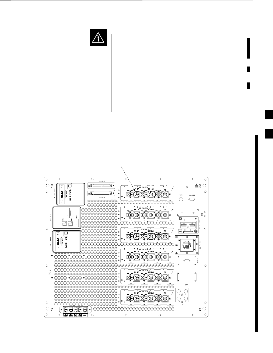
TX/RX Antenna Connections
Figure 4-1 identifies the Frame Transmit and Receive Antenna
Connections where measurements are to be taken.
FRONT
TX on TRF or
TX/RX MAIN on DRF
REAR
RX DIV RX MAIN on TRF
Not Used on DRF
ti-CDMA-WP-00214-v01-ildoc-ftw REF
Figure 4-1: TX and RX Antenna Connections on I/O Panel
4
Acceptance Tests – Test Set–up
4-4 1X SC 4812T Lite BTS Optimization/ATP FEB 2005
PRELIMINARY
Required Test Equipment
The following Test Equipment is required:
SLMF
SPower Meter (used with HP 8921A/600 and Advantest R3465)
SCommunications System Analyzer
SSignal Generator for FER Testing (required for all Communications
System Analyzers for 1X FER)
–Before installing any Test Equipment directly to any
BTS TX OUT Connector, verify that there are no
CDMA Channels keyed.
– At active sites, have the OMC–R/CBSC place the
carrier assigned to the LPA Modules under test OOS.
Failure to do so can result in serious personal injury
and/or equipment damage.
WARNING
The Test Equipment must be re–calibrated before using it
to perform the TX Acceptance Tests.
NOTE
Acceptance Test Equipment
Set–up
All ATP Testing
Perform the procedure in Table 4-1 to Set–up Test Equipment for all
tests..
4

Acceptance Tests – Test Set–up – continued
FEB 2005 1X SC 4812T Lite BTS Optimization/ATP 4-5
PRELIMINARY
Table 4-1: Set–up Test Equipment – TX Output Verify/Control Tests Procedure
nStep Action
1If it has not already been done, interface the LMF Computer to the BTS.
– Refer to Table 3-6 and Figure 3-3.
2If it has not already been done, start a GUI LMF Session and log into the BTS.
– Refer to Table 3-10.
3If it has not already been done, connect Test Equipment for Acceptance Testing.
– Refer to Figure 3-20, Figure 3-21, Figure 3-22, Figure 3-23, Figure 3-24, or Figure 3-25, as
applicable, for the Test Equipment and Antenna Duplexing being used.
* IMPORTANT
LMF–based Measurements factor into TX Test Test Cable Insertion Loss between the RF Modem
Frame and Test Equipment.
If additional attenuation, such as external TX Combiners, is inserted in the path, it must be
identified to the LMF by including it in the TX Test Cable Calibration.
– If this is not possible, include the attenuation in the TX Path by editing Test Cable Insertion
Loss Values (refer to Table 3-35).
– Failure to do this will result in test inaccuracies and potential for erroneous ATP failures
because the additional losses would not be compensated for in the test measurements.
4

Abbreviated (All–inclusive) Acceptance Tests
4-6 1X SC 4812T Lite BTS Optimization/ATP FEB 2005
PRELIMINARY
All–inclusive Tests
General
The all–inclusive Acceptance Tests are performed from the LMF GUI
Environment. These all–inclusive tests are called abbreviated ATPs
because they execute various combinations of individual Acceptance
Tests with a single command. This allows verification of multiple
aspects of BTS performance while minimizing time needed for
individual Test Set–up and initiation.
Abbreviated ATP Options
There are three abbreviated Acceptance Tests that evaluate different
performance aspects of the BTS. This allows the CFE to select testing to
meet the specific requirements for individual Maintenance and
Performance Verification situations. The following items summarize the
coverage of each Abbreviated Test.:
SAll TX/RX: Performs all transmit and receive ATPs on the selected
MCC Cards and BBX Cards.
SAll TX: Performs complete set of transmit ATPs on the selected MCC
Cards and BBX Cards. Testing is the equivalent of performing all of
the following individual tests:
–TX Mask Test
–Rho Test
–Pilot Time Offset Test
–Code Domain Power Test
SAll RX: Performs complete Receive ATP on the selected MCC Cards
and BBX Cards. Testing is the equivalent of performing the FER Test.
Abbreviated Acceptance Test Procedures
Procedures to accomplish each type of Abbreviated ATP are included in
the following subsections..
All TX/RX ATP Test Perform the procedure in Table 4-2 to perform the Abbreviated,
All–inclusive Transmit And Receive Test.
Table 4-2: All TX/RX Acceptance Test Procedure
nStep Action
1Set–up the Test Equipment initially for Abbreviated Tests as described in Table 4-1.
NOTE
If the LMF has been logged into the BTS with a different Multi–Channel Preselector setting than
the one to be used for this test, the LMF must be logged out of the BTS and logged in again with
the new Multi–Channel Preselector setting.
– Using the wrong MPC Setting can cause a false test failure.
table continued on next page
4

Abbreviated (All–inclusive) Acceptance Tests – continued
FEB 2005 1X SC 4812T Lite BTS Optimization/ATP 4-7
PRELIMINARY
Table 4-2: All TX/RX Acceptance Test Procedure
nActionStep
2Select the BBX Cards and MCC Cards to be tested.
3Click on Tests in the BTS Menu Bar, and select All TX/RX ATP... from the Pull–down Menu.
4Select the appropriate carrier(s) and sector(s) (carrier-bts#-sector#-carrier#) from those displayed
in the Channels/Carrier Pick List.
NOTE
To select multiple items, hold down the Shift or Ctrl Key while clicking on Pick List Items to
select multiple carrier(s)–sector(s).
5Verify that the correct Channel Number for the selected carrier is shown in the Carrier #
Channels Box.
– If it is not, obtain the latest bts–#.cdf (or bts–#.necf) and cbsc–#.CDF Files from the CBSC.
NOTE
If necessary, the correct Channel Number may be manually entered into the Carrier # Channels
Box.
6Select the appropriate RX Branch (BOTH, MAIN, or DIVersity) in the Pull–down Menu.
* IMPORTANT
The RX Main and Diversity Paths must be tested separately for this configuration because each
requires a different Multi–Coupler Preselector type to provide the proper Test Signal Gain.
NOTE
If a Companion Frame with the Inter–frame Diversity RX Cabling disconnected is being tested do
not select BOTH in this step.
7In the Rate Set Box, select the appropriate Data Rate (1=9600 3=9600 1X) from the Pull–down
Menu.
NOTE
The Rate Set selection of 3 is only available if 1X Cards are selected for the test.
8Enter the Channel Elements to be tested for the RX ATP in the Channel Element(s) Box.
– By default, all Channel Elements are specified.
– The Channel Element Numbers are 0.based; therefore, the first Channel Element is 0.
NOTE
Use one of the following methods to enter more than one Channel Element:
– Enter non–sequential Channel Elements separated by a comma and no spaces (for example;
0,5,15).
– Enter a range of sequential Channel Elements by typing the first and last Channel Elements
separated by two periods (for example; 0..15).
table continued on next page
4

Abbreviated (All–inclusive) Acceptance Tests – continued
4-8 1X SC 4812T Lite BTS Optimization/ATP FEB 2005
PRELIMINARY
Table 4-2: All TX/RX Acceptance Test Procedure
nActionStep
9In the Test Pattern Box, select the Test Pattern to use for the Acceptance Tests from the
Pull–down Menu.
– Refer to “Test Pattern Drop–down Pick List” under “TX Calibration and the LMF” in the Bay
Level Offset Calibration section of Chapter 3.
10 Click OK to display a Status Bar followed by a Directions Pop–up Window.
11 Execute the Cable Connection Directions as they are displayed, and click the Continue Button to
begin testing.
– As the ATP Process is completed, results will be displayed in the Status Report Window.
12 Click either the Save Results Button or the Dismiss Button.
* IMPORTANT
If Dismiss is used, the test results will not be saved in the Test Report File.
All TX ATP Test Perform the procedures in Table 4-3 to perform the Abbreviated,
All–inclusive Transmit Test.
Table 4-3: All TX Acceptance Test Procedure
nStep Action
1Set–up the Test Equipment for Abbreviated Tests per Table 4-1.
2Select the BBX Cards and MCC Cards to be tested.
3Click on Tests in the BTS Menu Bar, and select All TX ATP... from the Pull–down Menu.
4Select the appropriate carrier(s) and sector(s) (carrier-bts#-sector#-carrier#) from those displayed
in the Channels/Carrier Pick List.
NOTE
To select multiple items, hold down the Shift or Ctrl Key while clicking on Pick List Items to
select multiple carrier(s)–sector(s).
5Verify that the correct Channel Number for the selected carrier is shown in the Carrier #
Channels Box.
– If it is not, obtain the latest bts–#.cdf (or bts–#.necf) and cbsc–#.CDF Files from the CBSC.
NOTE
If necessary, the correct Channel Number may be manually entered into the Carrier # Channels
Box.
table continued on next page
4

Abbreviated (All–inclusive) Acceptance Tests – continued
FEB 2005 1X SC 4812T Lite BTS Optimization/ATP 4-9
PRELIMINARY
Table 4-3: All TX Acceptance Test Procedure
nActionStep
6In the Rate Set Box, select the appropriate Transfer Rate (1 = 9600, 3 = 9600 1X) from the
Pull–down Menu.
NOTE
The Rate Set Selection of 3 is only available if 1X Cards are selected for the test.
7In the Test Pattern Box, select the Test Pattern to use for the Acceptance Test from the Pull–down
Menu.
– Refer to “Test Pattern Drop–down Pick List” under “TX Calibration and the LMF” in the Bay
Level Offset Calibration section of Chapter 3.
8 Click OK to display a Status Bar followed by a Directions Pop–up Window.
9Execute the Cable Connection Directions as they are displayed, and click the Continue Button to
begin testing.
– As the ATP Process is completed, results will be displayed in the Status Report Window.
10 Click either the Save Results Button or the Dismiss Button.
* IMPORTANT
If Dismiss is used, the test results will not be saved in the Test Report File.
All RX ATP Test Perform the procedure in Table 4-4 to perform the Abbreviated,
All–inclusive Receive Test.
Table 4-4: All RX Acceptance Test Procedure
nStep Action
1Set–up the Test Equipment for Abbreviated Tests per Table 4-1.
NOTE
If the LMF has been logged into the BTS with a different Multi–Channel Preselector setting than
the one to be used for this test, the LMF must be logged out of the BTS and logged in again with
the new Multi–Channel Preselector setting.
– Using the wrong MPC Setting can cause a false test failure.
2Select the BBX Cards and MCC Cards to be tested.
3Click on Tests in the BTS Menu Bar, and select All RX ATP... from the Pull–down Menu.
4Select the appropriate carrier(s) and sector(s) (carrier-bts#-sector#-carrier#) from those displayed
in the Channels/Carrier Pick List.
NOTE
To select multiple items, hold down the Shift or Ctrl Key while clicking on Pick List Items to
select multiple carrier(s)–sector(s).
table continued on next page
4

Abbreviated (All–inclusive) Acceptance Tests – continued
4-10 1X SC 4812T Lite BTS Optimization/ATP FEB 2005
PRELIMINARY
Table 4-4: All RX Acceptance Test Procedure
nActionStep
5Verify that the correct Channel Number for the selected carrier is shown in the Carrier #
Channels Box.
– If it is not, obtain the latest bts–#.cdf (or bts–#.necf) and cbsc–#.CDF Files from the CBSC.
NOTE
If necessary, the correct Channel Number may be manually entered into the Carrier # Channels
Box.
6Select the appropriate RX Branch (BOTH, MAIN, or DIVersity) in the Pull–down Menu.
7In the Rate Set Box, select the appropriate Data Rate (1=9600, 2=14400, 3=9600 1X) from the
Pull–down Menu.
NOTE
The Rate Set Selection of 1 is only available if non–1X Cards are selected for the test.
The Rate Set Selection of 3 is only available if 1X Cards are selected for the test.
8Enter the Channel Elements to be tested for the RX ATP in the Channel Element(s) Box.
– By default, all Channel Elements are specified.
– The Channel Element Numbers are 0.based; that is the first Channel Element is 0.
NOTE
Use one of the following methods to enter more than one Channel Element:
– Enter non–sequential Channel Elements separated by a comma and no spaces (for example;
0,5,15).
– Enter a range of sequential Channel Elements by typing the first and last Channel Elements
separated by two periods (for example; 0..15).
9 Click OK to display a Status Bar followed by a Directions Pop–up Window.
10 Follow Cable Connection Directions as they are displayed, and click the Continue Button to
begin testing.
– When the ATP Process is completed, results will be displayed in the Status Report Window.
11 Click either the Save Results Button or the Dismiss Button.
* IMPORTANT
If Dismiss is used, the test results will not be saved in the Test Report File.
4

Individual Acceptance Tests
FEB 2005 1X SC 4812T Lite BTS Optimization/ATP 4-11
PRELIMINARY
RX and TX Testing
The following individual ATP Tests can be used to evaluate specific
aspects of BTS Operation against individual performance requirements.
All testing is performed using the LMF GUI Environment.
TX Testing
TX Tests verify any given Transmit Antenna Path and Output Power
Control. All tests are performed using the external, calibrated Test
Equipment. All measurements are made at the appropriate BTS TX
OUT Connector(s).
TX Tests verify TX Operation of the entire CDMA Forward Link using
selected BBX Cards assigned to respective Sector Antennas. Each BBX
is keyed–up to generate a CDMA Carrier (using both bbxlevel and
BLO) at the CDF File–specified Carrier Output Power Level.
RX Testing
RX Testing verifies Receive Antenna Paths for BBX Cards selected for
the test. All tests are performed using the external, calibrated Test
Equipment to inject a CDMA RF Carrier with all zero Longcode at the
specified RX Frequency at the appropriate BTS RX IN Connector(s).
RX Tests verify RX Operation of the entire CDMA Reverse Link using
all equipped MCC Cards assigned to all respective sector/antennas.
Individual Tests
Spectral Purity TX Mask
This test verifies that the transmitted CDMA Carrier Waveform
generated on each sector meets the transmit Spectral Mask Specification
(as defined in IS–97) with respect to the assigned CDF File Values.
Waveform Quality (Rho)
This test verifies that the transmitted Pilot Channel Element Digital
Waveform Quality (Rho) exceeds the minimum specified value in IS–97.
Rho represents the correlation between the actual and perfect CDMA
Modulation Spectrums. 1.0000 represents 100% (or perfect correlation).
Pilot Time Offset
The Pilot Time Offset is the difference between the Communications
System Test Set Measurement Interval (based on the BTS System Time
Reference) and the incoming block of transmitted data from the BTS
(Pilot only, Walsh Code 0).
Code Domain Power/Noise Floor
This test verifies the Code Domain Power Levels, that have been set for
all ODD numbered Walsh Channels, using the OCNS Command. This is
done by verifying that the ratio of PILOT divided by OCNS is equal to
10.2 + 2 dB, and, that the Noise Floor of all EVEN–numbered “OFF”
Walsh Channels measures < –27 dB for IS–95A/B and CDMA2000 1X
with respect to total CDMA Channel Power.
4

Individual Acceptance Tests – continued
4-12 1X SC 4812T Lite BTS Optimization/ATP FEB 2005
PRELIMINARY
BTS FER
This test verifies the BTS Receive FER on all Traffic Channel Elements
currently configured on all equipped MCC Cards (full rate at one percent
FER) at an RF Input Level of –119 dBm on the Main RX Antenna Paths
using operator–selected, CDF–equipped MCC Cards and BBX Cards at
the site. Diversity RX Antenna Paths are also tested using the lowest
equipped MCC Channel Element ONLY.
There are no pass/fail criteria associated with FER
Readings taken at levels below –119 dBm, other than to
verify that the FER Measurement reflects changes in the
RX Iinput Signal Level.
NOTE
4

TX Spectral Purity Transmit Mask Acceptance Test
FEB 2005 1X SC 4812T Lite BTS Optimization/ATP 4-13
PRELIMINARY
Background
Overview
This test verifies the Spectral Purity of each operator–selected BBX
Carrier keyed–up at a specific frequency specified in the current CDF.
All tests are performed using the external, calibrated Test Equipment
controlled by the same command. All measurements are made at the
appropriate BTS TX Antenna Connector..
Test Patterns
There are four operator–selectable Test Patterns with which this
Acceptance Test can be performed. The patterns, along with the channels
tested and Gain Setting for each, are listed in Table 3-40. Refer to “TX
Calibration and the LMF” in the Bay Level Offset Calibration section of
Chapter 3 for more information on the Test Patterns..
Equipment Operation During Testing
At least one MCC must be selected to perform the Standard, CDF Pilot,
and CDF Test Patterns. For these Test Patterns, Forward Links are
enabled for Synch Channel (SCH), Paging Channel (PCH), and Traffic
Channel (TCH) Elements from the selected MCC(s), as shown in
Table 3-40.
Gain is set for the applicable channels on each antenna as shown in the
table. The operator–selected BBX Cards will be keyed using a
BLO–corrected bbxlvl Value to generate a CDMA Carrier. RF Output
Power, as measured at the appropriate Frame TX Antenna Connector,
will be set to one of the following depending on the Operating
Frequency Spectrum.:
S800 MHz: 33.5 dBm
S1.9 GHz: 31.0 dBm
Test Measurements
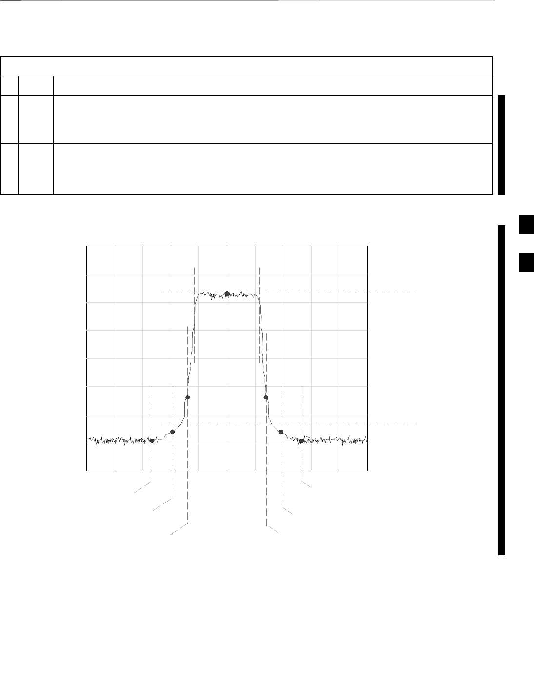
The Test Equipment will measure and return the attenuation level in dB
of all spurious and IM products with respect to the Mean Power of the
CDMA Channel measured in a 1.23 MHz bandwidth, verifying that
results meet system tolerances at the following test points. Refer to also
Figure 4-2):
SFor 800 MHz:
– At least –45 dB @ + 750 kHz from Center Frequency
– At least –45 dB @ – 750 kHz from Center Frequency
– At least –60 dB @ – 1980 kHz from Center Frequency
– At least –60 dB @ + 1980 kHz from Center Frequency
SFor 1.9 GHz:
– At least –45 dB @ + 885 kHz from Center Frequency
– At least –45 dB @ – 885 kHz from Center Frequency
– At least –55 dB @ – 1980 kHz from Center Frequency
– At least –55 dB @ + 1980 kHz from Center Frequency
4

TX Spectral Purity Transmit Mask Acceptance Test – continued
4-14 1X SC 4812T Lite BTS Optimization/ATP FEB 2005
PRELIMINARY
Redundant BBX Testing
The BBX will then de–key, and if selected, the Redundant BBX will be
assigned to the current TX Antenna Path under test. The test will then be
repeated..
Spectral Purity TX Mask
Acceptance Test
Perform the procedure in Table 4-5 to verify that the Transmit Spectral
Mask Specification on the TX Antenna Paths for the selected BBX
Cards.
Table 4-5: Spectral Purity Transmit Mask Test Procedure
nStep Action
1Set–up the Test Equipment for TX Acceptance Tests per Table 4-1.
2Select the BBX Cards to be tested.
3If the Test Pattern to be used is Standard, CDFPilot, or CDF; select at least one MCC.
– Refer to the “Test Pattern Drop–down Pick List” in the “BayLevel Offset Calibration” section
of Chapter 3.
4Click on Tests in the BTS Menu Bar, and select TX > TX Mask... from the Pull–down Menus.
5Select the appropriate carrier(s) and sector(s) (carrier-bts#-sector#-carrier#) from those displayed
in the Channels/Carrier Pick List.
NOTE
To select multiple items, hold down the Shift or Ctrl Key while clicking on Pick List Items to
select multiple carrier(s)–sector(s).
6Verify that the correct Channel Number for the selected carrier is shown in the Carrier #
Channels Box.
– If it is not, obtain the latest bts–#.cdf (or bts–#.necf) and cbsc–#.CDF Files from the CBSC.
NOTE
If necessary, the correct Channel Number may be manually entered into the Carrier # Channels
Box.
7If at least one MCC was selected in Step 3, select the appropriate Transfer Rate (1 = 9600, 3 =
9600 1X) from the Pull–down Menu in the Rate Set Box.
NOTE
The Rate Set Selection of 3 is only available if 1X Cards are selected for the test.
8In the Test Pattern Box, select the Test Pattern to use for the Calibration from the Pull–down
Menu.
– Refer to the “Test Pattern Drop–down Pick List” under “TX Calibration and the LMF” in the
Bay Level Offset Calibration section of Chapter 3.
9 Click OK to display a Status Bar followed by a Directions Pop–up Window.
table continued on next page
4
TX Spectral Purity Transmit Mask Acceptance Test – continued
FEB 2005 1X SC 4812T Lite BTS Optimization/ATP 4-15
PRELIMINARY
Table 4-5: Spectral Purity Transmit Mask Test Procedure
nActionStep
10 Follow the Cable Connection Directions as they are displayed, and click the Continue Button to
begin testing.
– As the ATP Process is completed, results will be displayed in a Status Report Window.
11 Click either the Save Results Button or the Dismiss Button.
* IMPORTANT
If Dismiss is used, the test results will not be saved in the Test Report File.
– 885 kHz + 885 kHz
Center Frequency Reference
Attenuation level of all
spurious and IM products
with respect to the Mean
Power of the CDMA Channel
.5 MHz Span/Div
Ampl 10 dB/Div
Mean CDMA Bandwidth
Power Reference
– 1980 kHz
+750 kHz
+ 1980 kHz
– 750 kHz
Figure 4-2: TX Mask Verification Spectrum Analyzer Display 4

TX Waveform Quality (Rho) Acceptance Test
4-16 1X SC 4812T Lite BTS Optimization/ATP FEB 2005
PRELIMINARY
Background
Overview
This test verifies the transmitted Pilot Channel Element Digital
Waveform Quality of each operator–selected BBX Carrier keyed–up at a
specific frequency specified in the current CDF. All tests are performed
using the external, calibrated Test Equipment controlled by the same
command. All measurements are made at the appropriate TX Antenna
Connector..
Equipment Operation During Testing
Pilot Gain will be set to 262 for each antenna, and all TCH Elements
from the MCC Cards will be forward–link disabled. The selected BBX
Cards will be keyed–up using both bbxlvl and BLO to generate a
CDMA Carrier (with Pilot Channel Element only, Walsh Code 0). RF
Output Power is set at 40 dBm as measured at the appropriate BTS TX
Antenna Connector..
Test Measurements
The Test Equipment will measure and return the Pilot Channel Element
Digital Waveform Quality (Rho) Percentage, verifying that the result
meets the following specification.:
Waveform Quality (Rho) should be > 0.912.
Redundant BBX Testing.
The BBX will then de–key, and if selected, the Redundant BBX will be
assigned to the current TX Antenna Path under test. The test will then be
repeated for the Redundant BBX..
Waveform Quality (Rho)
Acceptance Test
Perform the procedure in Table 4-6 to verify that the Pilot Channel
Element Waveform Quality (Rho) on the TX Antenna Paths for the
selected BBX Cards.
Table 4-6: Waveform Quality (Rho) Test Procedure
nStep Action
1Set–up the Test Equipment for TX Acceptance Tests per Table 4-1.
2Select the BBX Cards to be tested.
3Click on Tests in the BTS Menu Bar, and select TX > Rho... from the Pull–down Menus.
4Select the appropriate carrier(s) and sector(s) (carrier-bts#-sector#-carrier#) from those displayed
in the Channels/Carrier Pick List.
NOTE
To select multiple items, hold down the Shift or Ctrl Key while clicking on Pick List Items to
select multiple carrier(s)–sector(s).
table continued on next page
4

TX Waveform Quality (Rho) Acceptance Test – continued
FEB 2005 1X SC 4812T Lite BTS Optimization/ATP 4-17
PRELIMINARY
Table 4-6: Waveform Quality (Rho) Test Procedure
nActionStep
5Verify that the correct Channel Number for the selected carrier is shown in the Carrier #
Channels Box.
– If it is not, obtain the latest bts–#.cdf (or bts–#.necf) and cbsc–#.CDF Files from the CBSC.
NOTE
If necessary, the correct Channel Number may be manually entered into the Carrier # Channels
Box.
6 Click OK to display a Status Bar followed by a Directions Pop–up Window.
7Follow the Cable Connection Directions as they are displayed, and click the Continue Button to
begin testing.
– As the ATP Process is completed, results will be displayed in a Status Report Window.
8Click either the Save Results Button or the Dismiss Button.
* IMPORTANT
If Dismiss is used, the test results will not be saved in the Test Report File.
4

TX Pilot Time Offset Acceptance Test
4-18 1X SC 4812T Lite BTS Optimization/ATP FEB 2005
PRELIMINARY
Background
Overview
This test verifies the transmitted Pilot Channel Element Pilot Time
Offset of each operator–selected BBX Carrier keyed–up at a specific
frequency specified in the current CDF. All tests will be performed using
the external, calibrated Test Equipment controlled by the same
command. All measurements will be made at the BTS TX Antenna
Connector..
Equipment Operation During Testing
The Pilot Gain will be set to 262 for each antenna and all TCH
Elements from the MCC Cards will be forward–link disabled. The
selected BBX Cards will be keyed using both bbxlvl and BLO to
generate a CDMA Carrier (with Pilot Channel Element only, Walsh
Code 0). TX Power Output is set at 40 dBm as measured at the TX
Output..
Test Measurements
The Test Equipment will measure and return the Pilot Time Offset in ms,
verifying that results meet the following specification.:
Pilot Time Offset should be within 3 ms of the target PT Offset
(zeroĄms).
.Redundant BBX Testing –
The BBX will then de–key, and if selected, the Redundant BBX will be
assigned to the current TX Antenna Path under test. The test will then be
repeated for the Redundant BBX..
This test also executes and returns the TX Frequency and
TX Waveform Quality (Rho) ATP Tests, however, only
Pilot Time Offset results are written to the ATP Test
Report.
NOTE
Pilot Time Offset Acceptance
Test
Perform the procedure in Table 4-7 to verify that the Pilot Time Offset
on the TX Antenna Paths for the selected BBX Cards.
Table 4-7: Test Pilot Time Offset
nStep Action
1Set–up the Test Equipment for TX Acceptance Tests per Table 4-1.
2Select the BBX Cards to be tested.
table continued on next page
4

TX Pilot Time Offset Acceptance Test – continued
FEB 2005 1X SC 4812T Lite BTS Optimization/ATP 4-19
PRELIMINARY
Table 4-7: Test Pilot Time Offset
nActionStep
3Click on Tests in the BTS Menu Bar, and select TX > Pilot Time Offset... from the Pull–down
Menus.
4Select the appropriate carrier(s) and sector(s) (carrier-bts#-sector#-carrier#) from those displayed
in the Channels/Carrier Pick List.
NOTE
To select multiple items, hold down the Shift or Ctrl Key while clicking on Pick List Items to
select multiple carrier(s)–sector(s).
5Verify that the correct Channel Number for the selected carrier is shown in the Carrier #
Channels Box.
– If it is not, obtain the latest bts–#.cdf (or bts–#.necf) and cbsc–#.CDF Files from the CBSC.
NOTE
If necessary, the correct Channel Number may be manually entered into the Carrier # Channels
Box.
6 Click OK to display a Status Bar followed by a Directions Pop–up Window.
7Follow the Cable Connection Directions as they are displayed, and click the Continue Button to
begin testing.
– As the ATP Process is completed, results will be displayed in a Status Report Window.
8Click either the Save Results Button or the Dismiss Button.
* IMPORTANT
If Dismiss is used, the test results will not be saved in the Test Report File.
4

TX Code Domain Power/Noise Floor Acceptance Test
4-20 1X SC 4812T Lite BTS Optimization/ATP FEB 2005
PRELIMINARY
Background
Overview
This test verifies the Code Domain Power and Noise Floor of each
operator–selected BBX Carrier keyed at a specific frequency specified in
the current CDF. All tests are performed using the external, calibrated
Test Equipment controlled by the same command. All measurements are
made at the appropriate BTS TX Antenna Connector..
CDMA Channel Test Set–up
Pilot Gain should be set to 262 for each antenna and the selected MCC
Cards should be configured to supply all odd–numbered Walsh Code
Traffic Channel Elements by enabling Orthogonal Channel Noise Source
(OCNS) on all odd MCC Channel Elements (maximum 32 Full Rate
Channels with an OCNS Gain of 81).
– All even–numbered Walsh Code Traffic Channel Elements should
have OCNS disabled, and are considered “OFF”.
– Selected MCC Cards should be Forward–Link Enabled for the
antenna (sector) under test..
Equipment Operation During Testing
The BBX should be keyed–up using a BLO–corrected bbxlvl Value to
generate a CDMA Carrier consisting of Pilot and OCNS Channels. RF
Output Power, as measured at the appropriate Frame TX Antenna
Connector, is set at one of the following values depending on the
Operating Frequency Spectrum.:
– 800 MHz: 33.5 dBm
– 1.9 GHz: 31.0 dBm
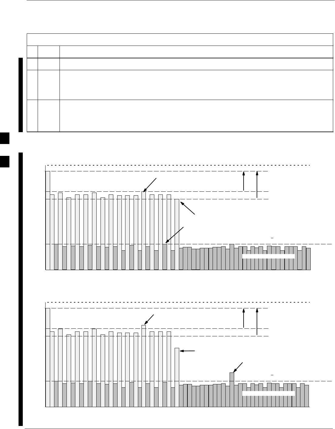
Test Measurements
The Test Equipment will measure and return the Channel Element
Power in dB of all specified Walsh Channels within the CDMA
spectrum. Additional calculations will be performed to verify that the
following parameters are met.
– Refer to Figure 4-3 for graphic representations.:
STraffic Channel Element Power Level will be verified by calculating
the ratio of Pilot Power to OCNS Gain of all Traffic Channels [Root
Sum of the Square (RSS) of each OCNS Gain divided by the Pilot
Power].
– This value should be 10.2 dB + 2.0 dB.
SNoise Floor (unassigned “OFF” even–numbered Walsh Channels) is
verified to be < –27 dB for IS–95A/B and CDMA2000 1X with
respect to total CDMA Channel Power.
4

TX Code Domain Power/Noise Floor Acceptance Test – continued
FEB 2005 1X SC 4812T Lite BTS Optimization/ATP 4-21
PRELIMINARY
When performing this test using the LMF and the MCC is
an MCC8E or MCC24E, the Redundant BBX may fail or
show marginal performance. This is due to a Timing
Mismatch that the LMF does not address. Performing this
test from the CBSC will not have this timing problem.
NOTE
Redundant BBX Testing
The BBX will then de–key, and if selected, the Redundant BBX will be
assigned to the current TX Antenna Path under test. The test will then be
repeated for the Redundant BBX. Upon completion of the test, OCNS
Channels will be disabled on the specified MCC Channel Elements..
Code Domain Power/Noise
Floor Test
Perform the procedure in Table 4-8 to verify the Code Domain
Power/Noise Floor of each selected BBX Carrier keyed–up at a specific
frequency.
Table 4-8: Code Domain Power/Noise Floor Test Procedure
nStep Action
1Set–up the Test Equipment for TX Acceptance Tests per Table 4-1.
2Select the BBX Cards and MCC Cards to be tested.
3Click on Tests in the BTS Menu Bar, and select TX > Code Domain Power... from the
Pull–down Menus.
4Select the appropriate carrier(s) and sector(s) (carrier-bts#-sector#-carrier#) from those displayed
in the Channels/Carrier Pick List.
NOTE
To select multiple items, hold down the Shift or Ctrl Key while clicking on Pick List Items to
select multiple carrier(s)–sector(s).
5Verify that the correct Channel Number for the selected carrier is shown in the Carrier #
Channels Box.
– If it is not, obtain the latest bts–#.cdf (or bts–#.necf) and cbsc–#.CDF Files from the CBSC.
NOTE
If necessary, the correct Channel Number may be manually entered into the Carrier # Channels
Box.
6If at least one MCC was selected in Step 3, select the appropriate Transfer Rate (1 = 9600, 3 =
9600 1X) from the Pull–down Menu in the Rate Set Box.
NOTE
The Rate Set selection of 3 is only available if 1X Cards are selected for the test.
table continued on next page
4
TX Code Domain Power/Noise Floor Acceptance Test – continued
4-22 1X SC 4812T Lite BTS Optimization/ATP FEB 2005
PRELIMINARY
Table 4-8: Code Domain Power/Noise Floor Test Procedure
nActionStep
7 Click OK to display a Status Bar followed by a Directions Pop–up Window.
8Follow the Cable Connection Directions as they are displayed, and click the Continue Button to
begin testing.
– As the ATP Process is completed, results will be displayed in a Status Report Window.
9Click either the Save Results Button or the Dismiss Button.
* IMPORTANT
If Dismiss is used, the test results will not be saved in the Test Report File.
Pilot Channel
Active channels
PILOT LEVEL
MAX OCNS SPEC.
MIN OCNS SPEC.
MAXIMUM NOISE FLOOR:
< –27 dB FOR IS–95A/B AND
CDMA2000 1X
Inactive channels
Walsh 0 1 2 3 4 5 6 7 ... 63
MAX OCNS
CHANNEL
MIN OCNS
CHANNEL
8.2 dB 12.2 dB
MAX NOISE
FLOOR
Pilot Channel
Active channels
PILOT LEVEL
MAX OCNS SPEC.
MIN OCNS SPEC.
MAXIMUM NOISE FLOOR:
< –27 dB FOR IS–95A/B AND
CDMA2000 1X
Inactive channels
Walsh 0 1 2 3 4 5 6 7 ... 63
FAILURE – DOES NOT
MEET MIN OCNS SPEC.
FAILURE – EXCEEDS
MAX OCNS SPEC. 8.2 dB 12.2 dB
FAILURE – EXCEEDS MAX
NOISE FLOOR SPEC.
Code Domain Power/Noise Floor (OCNS Pass) Example
Figure 4-3: Code Domain Analyzer CD Power/Noise Floor Display Examples
Code Domain Power/Noise Floor (OCNS Failure) Example
4

RX FER Acceptance Test
FEB 2005 1X SC 4812T Lite BTS Optimization/ATP 4-23
PRELIMINARY
Background
Overview
This test verifies the BTS Frame Erasure Rate (FER) on all TCHs
currently configured on operator–selected MCC Cards (full rate at 1%
FER) at –119 dBm. All tests are performed using the external, calibrated
Test Equipment as the Signal Source controlled by the same command.
Measurements are made at the specified BTS RX Antenna Connection..
Equipment Operation During Testing
The Pilot Gain on each MCC will be set to 262 for each TX Antenna,
and the Forward Link for all TCH Elements from the MCC Cards will
be enabled. Appropriate BBX(s) must be keyed in order to enable the
RX Receive Circuitry. Operator–selected BBX Cards will be keyed
using only bbxlvl, to generate a CDMA Carrier with Pilot Channel
Element only.
Transmit Power Output is set at –40 dBm. Test Equipment Output Power
is set so that the received power at the BBX is –119 dBm. The Final
Output Power Setting of the Test Equipment takes into account the MPC
type, BTS RF Path Losses, and test Test Cable Insertion Losses. If
selected, the Redundant BBX will be assigned to the current RX
Antenna Paths under test..
Test Measurements
The LMF will prompt the MCC Channel Element under test to measure
all–zero Longcode and provide the FER report on the selected active
MCC on the Reverse Link for the Main and, if selected, Diversity RX
Antenna Paths. Results are evaluated to ensure they meet the following
specification.:
FER returned less than 1% and Total Frames measured is 1500
Redundant BBX Testing
After the test, the BBX and the Test Equipment will be de–keyed to shut
down the Pilot Signal and the active Channel Element, respectively. If
the Redundant BBX was tested, BBXR assignment to an active sector
will also be reset..
FER Acceptance Test
Perform the procedure in Table 4-9 to verify the FER on RX Antenna
Paths using selected MCC Cards and BBX Cards.
4

RX FER Acceptance Test – continued
4-24 1X SC 4812T Lite BTS Optimization/ATP FEB 2005
PRELIMINARY
Table 4-9: FER Test Procedure
nStep Action
1Set–up the Test Equipment for RX Acceptance Tests per Table 4-1.
2If the LMF has been logged into the BTS with a different Multi–Channel Preselector setting than
the one to be used for this test, the LMF must be logged out of the BTS and logged in again with
the new Multi–Channel Preselector Setting.
* IMPORTANT
Using the wrong MPC Setting can cause a false test failure.
3Select the BBX Cards and MCC Cards to be tested.
4Click on Tests in the BTS Menu Bar, and select RX > FER... from the Pull–down Menu.
5Select the appropriate carrier(s) and sector(s) (carrier-bts#-sector#-carrier#) from those displayed
in the Channels/Carrier Pick List.
NOTE
To select multiple items, hold down the Shift or Ctrl Key while clicking on Pick List Items to
select multiple carrier(s)–sector(s).
6Verify that the correct Channel Number for the selected carrier is shown in the Carrier #
Channels Box.
– If it is not, obtain the latest bts–#.cdf (or bts–#.necf) and cbsc–#.CDF Files from the CBSC.
NOTE
If necessary, the correct Channel Number may be manually entered into the Carrier # Channels
Box.
7Select the appropriate RX Branch (Both, Main, or Diversity) in the Pull–down Menu.
8In the Rate Set Box, select the appropriate Data Rate (1=9600, 2=14400, 3=9600 1X) from the
Pull–down Menu.
NOTE
The Rate Set selection of 2 is only available if non–1X Cards are selected for the test.
The Rate Set selection of 3 is only available if 1X Cards are selected for the test.
9 Click OK to display a Status Bar followed by a Directions Pop–up Window.
10 Follow Cable Connection Directions as they are displayed, and click the Continue Button to
begin testing.
– As the ATP Process is completed, results will be displayed in the Status Report Window.
11 Click either the Save Results Button or the Dismiss Button.
* IMPORTANT
If Dismiss is used, the test results will not be saved in the Test Report File.
4

Generating an ATP Report
FEB 2005 1X SC 4812T Lite BTS Optimization/ATP 4-25
PRELIMINARY
Background
Each time an ATP Test is run, ATP Data is updated and must be saved to
an ATP Report File using the Save Results Button to close the Status
Report Window. The ATP Report File will not be updated if the Status
Report Window is closed using the Dismiss Button.
ATP Report
A separate report is created for each BTS and includes the following for
each test:
STest Name
SPASS or FAIL
SDescription Information (if applicable)
SBBX Number
SChannel Number
SCarrier Number
SSector Number
SUpper Test Limit
SLower Test Limit
STest Result
STime Stamp
SDetails/Warning Information (if applicable)
Perform the procedures in the Table 4-10 to view and create a printable
file for the ATP Report.
Table 4-10: ATP Report Generation Procedure
nStep Action
1Click on the Login Tab (if not in the forefront).
2Click on the desired BTS in the Available Base Stations Pick List to select it.
3Click on the Report Button.
4If a printable file is not needed, click on the Dismiss Button.
5If a printable file is required, perform the following actions.
5a Select the desired file type (text, comma–delimited, HTML) for the report file from the Pull–down
Menu at the bottom of the screen.
5b Click the Save Button to save the file.
– The file will be saved in the selected format in the bts–# folder for the BTS selected.
4

Updating Calibration Data Files
4-26 1X SC 4812T Lite BTS Optimization/ATP FEB 2005
PRELIMINARY
Software Release Caveats
Software Release R2.16.5.x allows the user to load the Calibration File
from the LMF directly onto the MGLI. The MGLI will then FTP the
new Calibration File to the OMC–R, thereby eliminating the need for the
user to place the Calibration File at the OMC–R.
Copy and Load Cal File to the
CBSC
After completing the TX Calibration and audit, updated CAL File
information must be moved from the LMF Windows environment back
to the CBSC, a UNIX environment. The following procedures detail
moving files from one environment to the other.
Copying CAL Files from LMF to a Diskette
Perform the procedures in Table 4-11 to copy the CAL Files from an
LMF Computer to a 3.5 diskette.
Table 4-11: Copy CAL Files to a Diskette Procedure
nStep Action
1 With Windows running on the LMF Computer, insert a disk into Drive A:\.
2Launch the Windows Explorer Application Program from the Start > Programs Menu List.
3Select the applicable <x>:\<lmf home directory/cdma/bts–# Folder.
4Drag the bts–#.cal file to Drive A.
5Repeat Steps 3 and 4, as required, for other bts–# Folders.
Copying CAL Files from Diskette to the CBSC
Perform the procedures in Table 4-12 to copy CAL Files from a diskette
to the CBSC.
Table 4-12: Copy CAL Files from Diskette to the CBSC Procedure
nStep Action
1Log into the CBSC on the OMC–R UNIX Workstation using your Account Name and Password.
2Place the diskette containing the Calibration File(s) into the Workstation Diskette Drive.
3 Enter EJECT –q and press the Enter Key.
4 Enter mount and press the Enter Key.
NOTE
SVerify that the message “floppy/no_name” is displayed on the last line.
– If the EJECT Command was previously entered, floppy/no_name will be appended with a
number.
– Use the explicit floppy/no_name reference displayed.
table continued on next page
4

Updating Calibration Data Files – continued
FEB 2005 1X SC 4812T Lite BTS Optimization/ATP 4-27
PRELIMINARY
Table 4-12: Copy CAL Files from Diskette to the CBSC Procedure
nActionStep
5 Enter cd /floppy/no_name and press the Enter Key.
6 Enter ls –lia and press the Enter Key.
– Verify that the bts–#.cal file filename appears in the displayed Directory Listing.
7 Enter cd and press the Enter Key.
8 Enter pwd and press the Enter Key.
– Verify that the displayed response shows the correct Home Directory (/home/<user’s name>).
9 With Solaris versions of UNIX, create a UNIX–formatted version of the bts–#.cal file in the Home
Directory by performing the following actions.
9a Type the following command:
dos2unix /floppy/no_name/bts–#.cal bts–#.cal
Where: # = BTS Number for which the CAL File was created
9b Press the Enter Key.
NOTE
Other versions of UNIX do not support the dos2unix Command. In these cases, use the UNIX
cp (Copy) Command.
– The copied files contain DOS Line Feed Characters that must be edited out with a UNIX Text
Editor.
10 Enter ls –l *.cal and press the Enter Key. Verify that the CAL Files have been copied.
– Verify that all CAL Files to be transferred appear in the displayed listing.
11 Type EJECT, and press the Enter Key.
12 Remove the diskette from the workstation.
4

Updating Calibration Data Files – continued
4-28 1X SC 4812T Lite BTS Optimization/ATP FEB 2005
PRELIMINARY
Notes
4

FEB 2005 1X SC 4812T Lite BTS Optimization/ATP
PRELIMINARY
Chapter 5: Prepare to Leave the Site
Table of Contents
Prepare to Leave the Site 5-3 . . . . . . . . . . . . . . . . . . . . . . . . . . . . . . . . . . . . . . . . . .
External Test Equipment Removal 5-3 . . . . . . . . . . . . . . . . . . . . . . . . . . . .
Bringing Modules into Service with the LMF 5-3 . . . . . . . . . . . . . . . . . . .
LMF Removal 5-4 . . . . . . . . . . . . . . . . . . . . . . . . . . . . . . . . . . . . . . . . . . . .
Re–connect BTS T1/E1 Spans 5-5 . . . . . . . . . . . . . . . . . . . . . . . . . . . . . . .
Final Checks Before Leaving Site 5-5 . . . . . . . . . . . . . . . . . . . . . . . . . . . . .
Reset All Devices and Initialize Site Remotely 5-6 . . . . . . . . . . . . . . . . . . .
5

Table of Contents – continued
1X SC 4812T Lite BTS Optimization/ATP FEB 2005
PRELIMINARY
Notes
5

Prepare to Leave the Site
FEB 2005 1X SC 4812T Lite BTS Optimization/ATP 5-3
PRELIMINARY
External Test Equipment
Removal Perform the procedure in Table 5-1 to disconnect the Test Equipment and
configure the BTS for active service.
Table 5-1: External Test Equipment Removal Procedure
nStep Action
n WARNING
Make sure that no BBX Cards are keyed before performing this procedure.
– Failure to do so can result in personal injury and damage to BTS LPA Modules.
1At the rear of the frame, disconnect all external Test Equipment from all TX and RX Connectors.
2Reconnect and visually inspect all TX and RX Antenna Feed Lines at the Frame RF Interface
Panel.
* IMPORTANT
Verify that all Sector Antenna Feed Lines are connected to the correct Antenna Connectors on the
frame. Crossed Antenna Cables will degrade Call Processing.
Bringing Modules into Service
with the LMF
Whenever possible, have the CBSC/MM bring up the site
and enable all devices on the BTS.
NOTE
If a Reason Code is present and/or data should/could not be loaded
remotely from the CBSC, follow the steps outlined in Table 5-2 as
required to bring BTS Processor Modules from an OOS State to an INS
State.
Table 5-2: Bring Modules into Service Procedure
nStep Action
1In the LMF GUI Environment, select the device(s) to be enabled by clicking on each one.
* IMPORTANT
SThe MGLI and CSM must be INS_ACTIVE (bright green) before an MCC can be enabled.
2Enable the Processor Cards in the following order.
1. MGLI
2. CSM Cards
3. MCC Cards
table continued on next page
5

Prepare to Leave the Site – continued
5-4 1X SC 4812T Lite BTS Optimization/ATP FEB 2005
PRELIMINARY
Table 5-2: Bring Modules into Service Procedure
nActionStep
3Click on Device in the BTS Menu Bar, and select Enable from the Pull–down Menu.
– A Status Report Window is displayed.
* IMPORTANT
If a BBX is selected, a Transceiver Parameters Window is displayed to collect Keying
Information. Do not enable the BBX.
4 Click Cancel to close the Transceiver Parameters Window, if applicable.
5 Click OK to close the Status Report Window.
– Bright Green is the color of devices that successfully change to INS.
LMF Removal
Perform the procedure in Table 5-3 as required to terminate the LMF
GUI Session and remove the LMF Computer.
Table 5-3: Terminate the LMF Session and Remove the LMF Procedure
nStep Action
! CAUTION
Do not power down the LMF Computer without performing the procedure below; corrupted
and/or lost Data Files may result.
1Log out of all BTS Sessions and exit the LMF by clicking on File in the LMF Window Menu Bar
and selecting Logout and Exit from the Pull–down Menu.
2In the Windows Task Bar, click Start and select Shutdown.
3 Click Yes when the Shut Down Windows Message appears.
4Wait for the system to shut down and the screen to go blank.
5Disconnect the LMF Computer Ethernet Port from the BTS Frame.
6Disconnect the LMF Computer Serial Port, the RS–232–to–GPIB Interface Box, and the GPIB
Cables as required for equipment transport.
5

Prepare to Leave the Site – continued
FEB 2005 1X SC 4812T Lite BTS Optimization/ATP 5-5
PRELIMINARY
Re–connect BTS T1/E1 Spans
Before leaving the site, connect any T1 or E1 Span Connectors removed
previously to allow the LMF to control the BTS. Refer to Table 5-4 and
Figure 3-2.
Table 5-4: T1 or E1 Spans Re–connection Procedure
nStep Action
1Re–connect any disconnected Span Connectors to the Span I/O A and B Boards.
2If equipped, ensure that the CSU is powered ON.
3Verify Span Status, ensuring that the OMC–R/CBSC can communicate with the BTS.
Final Checks Before Leaving
Site
Make sure all requirements listed in Table 5-5 are completed before
leaving the site.
Table 5-5: Check Before Leaving the Site Procedure
nStep Action
1For AC Frame only:
Validate the Vtrim Signal Cabling.
2Ensure that the Battery Voltage is 27 Volts at 25C.
– If external batteries are provided by the Customer, ensure that the Customer Circuit Breaker is
closed.
NOTE
A Low Voltage Disconnect must be in series with the external batteries.
3Verify that no Alarm Conditions are being reported to the CBSC after all Cabinet Doors are
closed.
5

Prepare to Leave the Site – continued
5-6 1X SC 4812T Lite BTS Optimization/ATP FEB 2005
PRELIMINARY
Reset All Devices and Initialize
Site Remotely
Devices in the BTS should not be left with Data and Code Loaded from
the LMF. The Configuration Data and Code Loads used for normal
operation could be different from those stored in the LMF Files.
The following two procedure, one for Circuit Backhaul and the other for
Packet Backhaul, are provided to remotely reset the BTS Devices and
then initialize the BTS.
Circuit Backhaul Remote Reset and Initialization
Perform the procedure in Table 5-6 to remotely reset the BTS Devices in
a Circuit Backhaul BTS, and then remotely initialize the same BTS.
Table 5-6: Circuit Backhaul Remote Reset and Initialization Procedure
nStep Action
1Terminate the LMF Session by performing the procedure in Table 5-3.
2Reconnect the Spans by performing the procedure in Table 5-4.
3From the BTS Site, contact the OMC–R and request the operator to perform a BTS Reset.
OR
At the BTS Site, perform the actions in Step 4 through Step 6.
4Unseat one GLI Card and wait for 30 seconds.
5Re–seat the GLI and wait for it to complete its Initialization Process (this takes about one minute).
6Repeat Step 4 and Step 5 for the second GLI.
7Depending on the number and configuration of installed operational GLI Cards, perform the
following actions.
SBTS with Redundant GLI Cards, proceed to Step 8.
SBTS with a non–Redundant GLI or a non–operational Redundant GLI, proceed to Step 9.
8From the OMC–R, run the ACTIVATE Command on the BTS.
– After the ACTIVATE Command has been executed, proceed to Step 10.
9From the OMC–R, perform the following actions.
9a ACTIVATE the GLI.
– This action sets the NextLoad Attribute for the GLI to work with the current BSS Software
Version.
9b Disable the GLI.
9c Enable the GLI.
– This action allows the MM to load the software version specified by the NextLoad Attribute.
9d Once the GLI is INS_ACT, contact the OMC–R to again run the ACTIVATE Command on the
BTS.
table continued on next page
5

Prepare to Leave the Site – continued
FEB 2005 1X SC 4812T Lite BTS Optimization/ATP 5-7
PRELIMINARY
Table 5-6: Circuit Backhaul Remote Reset and Initialization Procedure
nActionStep
10 Once the GLI Cards are loaded with the specified Code Version, the active GLI will verify and
update, as required, its RAM.
– Also, if necessary, ROM Code Loads for the installed CSM, MCC, and BBX Cards using the
DLM.
11 After all activities at the site have been completed, contact the OMC–R to confirm that the BTS is
under OMC–R control.
Packet Backhaul Remote Reset and Initialization
Perform the procedure in Table 5-7 to remotely reset the BTS Devices in
a Packet Backhaul BTS, and then remotely initialize the same BTS.
Table 5-7: Packet Backhaul Remote Reset and Initialization Procedure
nStep Action
1Terminate the LMF Session by performing the procedure in Table 5-3.
2Reconnect the Spans by performing the procedure in Table 5-4.
3Determine which of the two types of PREACTIVATE Load Processes is applicable to your
situation.
Rolling Upgrade: This Load Process is only available when the BTS Cards are populated for Full
Redundancy as applicable.
Quick Reboot: This Load Process is used when Redundancy for the BTS Cards is not available.
– The GLI3 disables and reboots to the new Load. This will cause all the other cards to go out
of service.
– Once it is rebooted, the GLI3 determines which cards require a new Load and then downloads
the cards in the order that they establish communication with the GLI3 following their reboot.
– The GLI3 can reload up to 16 devices simultaneously.
4From the BTS Site, contact the OMC–R and request the operator to PREACTIVATE the BTS to
the required software version for the BSS.
5After all activities at the site have been completed, contact the OMC–R to confirm that the BTS is
under OMC–R control.
5

Prepare to Leave the Site – continued
5-8 1X SC 4812T Lite BTS Optimization/ATP FEB 2005
PRELIMINARY
Notes
5

FEB 2005 1X SC 4812T Lite BTS Optimization/ATP
PRELIMINARY
Chapter 6: Troubleshooting
Table of Contents
Basic Troubleshooting: Overview 6-1 . . . . . . . . . . . . . . . . . . . . . . . . . . . . . . . . . . .
Overview 6-1 . . . . . . . . . . . . . . . . . . . . . . . . . . . . . . . . . . . . . . . . . . . . . . . .
Troubleshooting: Installation 6-2 . . . . . . . . . . . . . . . . . . . . . . . . . . . . . . . . . . . . . . .
Cannot Log into Cell-Site 6-2 . . . . . . . . . . . . . . . . . . . . . . . . . . . . . . . . . . .
Force LAN A Active
(LMF Connection at I/O Panel LAN Connector) 6-3 . . . . . . . . . . . . . . . .
Force LAN A Active
(LMF Connection at Service Shelf LAN Connector) 6-4 . . . . . . . . . . . . .
Set the GLI IP Address 6-5 . . . . . . . . . . . . . . . . . . . . . . . . . . . . . . . . . . . . .
Cannot Communicate with Power Meter 6-7 . . . . . . . . . . . . . . . . . . . . . . .
Cannot Communicate with Communications System Analyzer 6-7 . . . . . .
Cannot Communicate with Signal Generator 6-8 . . . . . . . . . . . . . . . . . . . .
Troubleshooting: Download 6-9 . . . . . . . . . . . . . . . . . . . . . . . . . . . . . . . . . . . . . . . .
Troubleshooting: Download 6-9 . . . . . . . . . . . . . . . . . . . . . . . . . . . . . . . . .
Cannot Download DATA to Any Device (Card) 6-10 . . . . . . . . . . . . . . . . . .
Cannot ENABLE Device 6-10 . . . . . . . . . . . . . . . . . . . . . . . . . . . . . . . . . . . .
LPA Errors 6-11 . . . . . . . . . . . . . . . . . . . . . . . . . . . . . . . . . . . . . . . . . . . . . . .
Troubleshooting: Calibration 6-12 . . . . . . . . . . . . . . . . . . . . . . . . . . . . . . . . . . . . . . .
Bay Level Offset Calibration Failure 6-12 . . . . . . . . . . . . . . . . . . . . . . . . . . .
Calibration Audit Failure 6-13 . . . . . . . . . . . . . . . . . . . . . . . . . . . . . . . . . . . .
Basic Troubleshooting: RF Path Fault Isolation 6-14 . . . . . . . . . . . . . . . . . . . . . . . . .
Overview 6-14 . . . . . . . . . . . . . . . . . . . . . . . . . . . . . . . . . . . . . . . . . . . . . . . .
If Every Test Fails 6-14 . . . . . . . . . . . . . . . . . . . . . . . . . . . . . . . . . . . . . . . . .
Verify BLO Check Box 6-15 . . . . . . . . . . . . . . . . . . . . . . . . . . . . . . . . . . . . .
Single–Sided BLO Check Box 6-15 . . . . . . . . . . . . . . . . . . . . . . . . . . . . . . .
If Faults Are Isolated 6-15 . . . . . . . . . . . . . . . . . . . . . . . . . . . . . . . . . . . . . . .
Fault Isolation Flowchart 6-15 . . . . . . . . . . . . . . . . . . . . . . . . . . . . . . . . . . . .
Flowchart Prerequisites 6-16 . . . . . . . . . . . . . . . . . . . . . . . . . . . . . . . . . . . . .
TX Power Output Fault Isolation Flowchart 6-17 . . . . . . . . . . . . . . . . . . . . .
Troubleshooting: Transmit ATP 6-18 . . . . . . . . . . . . . . . . . . . . . . . . . . . . . . . . . . . . .
BTS Passed Reduced ATP Tests but Has Forward Link Problem in
Normal Operation 6-18 . . . . . . . . . . . . . . . . . . . . . . . . . . . . . . . . . . . . . . . .
Cannot Perform TX Mask Measurement 6-18 . . . . . . . . . . . . . . . . . . . . . . . .
Cannot Perform Rho or Pilot Time Offset Measurement 6-18 . . . . . . . . . . .
Cannot Perform Code Domain Power and Noise Floor Measurement 6-19 .
Troubleshooting: Receive ATP 6-20 . . . . . . . . . . . . . . . . . . . . . . . . . . . . . . . . . . . . . .
Multi–FER Test Failure 6-20 . . . . . . . . . . . . . . . . . . . . . . . . . . . . . . . . . . . . .
6

Table of Contents – continued
1X SC 4812T Lite BTS Optimization/ATP FEB 2005
PRELIMINARY
Troubleshooting: CSM Checklist 6-21 . . . . . . . . . . . . . . . . . . . . . . . . . . . . . . . . . . . .
Problem Description 6-21 . . . . . . . . . . . . . . . . . . . . . . . . . . . . . . . . . . . . . . .
Intermittent 19.6608 MHz Reference Clock / GPS Receiver Operation 6-21
No GPS Reference Source 6-21 . . . . . . . . . . . . . . . . . . . . . . . . . . . . . . . . . . .
Checksum Failure 6-21 . . . . . . . . . . . . . . . . . . . . . . . . . . . . . . . . . . . . . . . . .
GPS Bad RX Message Type 6-21 . . . . . . . . . . . . . . . . . . . . . . . . . . . . . . . . .
CSM Reference Source Configuration Error 6-22 . . . . . . . . . . . . . . . . . . . . .
Takes Too Long for CSM to Come INS 6-22 . . . . . . . . . . . . . . . . . . . . . . . .
Troubleshooting: SCCP Backplane 6-23 . . . . . . . . . . . . . . . . . . . . . . . . . . . . . . . . . .
Introduction 6-23 . . . . . . . . . . . . . . . . . . . . . . . . . . . . . . . . . . . . . . . . . . . . . .
Connector Functionality 6-23 . . . . . . . . . . . . . . . . . . . . . . . . . . . . . . . . . . . .
SCCP Backplane Troubleshooting Procedure 6-24 . . . . . . . . . . . . . . . . . . . .
Digital Control Problems 6-25 . . . . . . . . . . . . . . . . . . . . . . . . . . . . . . . . . . . .
DC Power Problems 6-27 . . . . . . . . . . . . . . . . . . . . . . . . . . . . . . . . . . . . . . .
TX and RX Signal Routing Problems 6-28 . . . . . . . . . . . . . . . . . . . . . . . . . .
Troubleshooting: RFDS 6-29 . . . . . . . . . . . . . . . . . . . . . . . . . . . . . . . . . . . . . . . . . . .
Introduction 6-29 . . . . . . . . . . . . . . . . . . . . . . . . . . . . . . . . . . . . . . . . . . . . . .
All Tests Fail 6-29 . . . . . . . . . . . . . . . . . . . . . . . . . . . . . . . . . . . . . . . . . . . . .
All RX and TX Paths Fail 6-29 . . . . . . . . . . . . . . . . . . . . . . . . . . . . . . . . . . .
All Tests Fail on a Single Antenna 6-30 . . . . . . . . . . . . . . . . . . . . . . . . . . . .
Module Front Panel LED Indicators and Connectors 6-31 . . . . . . . . . . . . . . . . . . . . .
Module Status Indicators 6-31 . . . . . . . . . . . . . . . . . . . . . . . . . . . . . . . . . . . .
Module LED Status (except GLI3, CSM, BBX, MCC) 6-31 . . . . . . . . . . . .
Power Supply Module LED Status Combinations 6-31 . . . . . . . . . . . . . . . .
CSM LED Status Combinations 6-32 . . . . . . . . . . . . . . . . . . . . . . . . . . . . . .
GLI3 LED Status Combinations 6-34 . . . . . . . . . . . . . . . . . . . . . . . . . . . . . .
GLI3 Pushbutton and Connectors 6-36 . . . . . . . . . . . . . . . . . . . . . . . . . . . . .
BBX LED Status Combinations 6-37 . . . . . . . . . . . . . . . . . . . . . . . . . . . . . .
MCC LED Status Combinations 6-38 . . . . . . . . . . . . . . . . . . . . . . . . . . . . . .
CLPA LED Status Combinations 6-40 . . . . . . . . . . . . . . . . . . . . . . . . . . . . .
Troubleshooting: Span Control Link 6-42 . . . . . . . . . . . . . . . . . . . . . . . . . . . . . . . . .
Span Problems (No Control Link) 6-42 . . . . . . . . . . . . . . . . . . . . . . . . . . . . .
Set BTS Site Span Configuration 6-44 . . . . . . . . . . . . . . . . . . . . . . . . . . . . .
6

Basic Troubleshooting: Overview
FEB 2005 1X SC 4812T Lite BTS Optimization/ATP 6-1
PRELIMINARY
Overview
The information in this chapter addresses some of the scenarios likely to
be encountered by Customer Field Engineering (CFE) Team Members
while performing BTS Optimization and Acceptance Testing. This
Troubleshooting Guide was created as an interim reference document for
use in the field. It provides “what to do if” basic troubleshooting
suggestions when the BTS Equipment does not perform according to the
procedures documented in the manual.
Comments are consolidated from inputs provided by CFEs and
information gained from experience in Motorola Labs and Classrooms.
6

Troubleshooting: Installation
6-2 1X SC 4812T Lite BTS Optimization/ATP FEB 2005
PRELIMINARY
Cannot Log into Cell-Site
Table 6-1: Login Failure Troubleshooting Procedures
nStep Action
1If the LED on either GLI is solid RED, it implies a hardware failure.
Reset the GLI by re-seating it.
– If re–seating the MGLI does not fix the problem, proceed to Step 2.
2Install a GLI Card in the Redundant GLI Slot and retry.
NOTE
A Red LED may also indicate no termination on an External LAN Connector (I/O Panel at the top
of the frame or at the top of a Logical BTS Frame).
3Circuit BTS:
Verify that the Span Line is disconnected at the Span I/O Card.
Circuit or Packet BTS:
Verify that the OMC–R has disabled the BTS.
4“Ping” the INS_ACTIVE GLI.
– Refer to Table 3-15.
5Verify that the LMF is connected to the Primary LAN (LAN A) at one of the following locations.
– The Service Shelf below the SCCP Cage.
– The BTS I/O Panel at the top of the frame.
6If LAN A is not the active LAN, force a LAN Switch to LAN A by performing the procedure in
Table 6-2.
7Verify that the LMF was configured properly.
8If a Xircom Parallel BNC LAN Interface is being used, verify that the BTS-LMF Cable is RG-58
(flexible black cable, less than 2.5 feet in length).
9Verify that the External LAN Connectors are properly terminated at either of the following two
locations.
– Service Shelf
– BTS I/O Panel at the top of the frame.
10 If the LMF is connected to the Primary LAN at the Service Shelf, verify that a T-Adapter is not
used on the LMF Computer or on the Ethernet Hub/Adapter Connector.
11 If the LMF is connected to the Primary LAN at the Service Shelf, try connecting to the Ethernet
Out Port on the I/O Panel (top of frame) using the procedure in Table 3-7.
12 Re-boot the LMF and retry.
13 Re-seat the INS_ACTIVE GLI and retry.
table continued on next page
6

Troubleshooting: Installation – continued
FEB 2005 1X SC 4812T Lite BTS Optimization/ATP 6-3
PRELIMINARY
Table 6-1: Login Failure Troubleshooting Procedures
nActionStep
14 Re-seat the INS_ACT GLI and retry.
15 Verify that the GLI IP Addresses are configured properly by performing the procedure in
Table 6-4.
Force LAN A Active (LMF
Connection at I/O Panel LAN
Connector)
Table 6-2: Procedure to Force Ethernet LAN A to Active State as Primary LAN
(LMF Connection at I/O Panel LAN Connector)
nStep Action
1If LAN A is not the active LAN, make certain all External LAN Connectors are either terminated
with 50Ω Loads or cabled to another frame.
2If it has not already been done, connect the LMF Computer to the Stand–alone or Starter Frame,
as applicable (Table 3-6).
3If it has not already been done, start a GUI LMF Session and log into the BTS on the active LAN
(Table 3-10).
4Remove the 50Ω Terminator from the LAN B IN Connector on the I/O Panel of the Stand–alone
or Starter Frame.
– The LMF Session will become inactive.
5Log into the BTS with the LMF (Table 3-10).
– Forcing LAN A to the INS_ACTIVE State was successful if the LMF can log into the BTS
and status any card in the cage.
SIf LAN A was successfully forced to an active state, skip to Step 12.
6With the 50Ω Terminator still removed from the LAN B IN Connector, remove the 50Ω
Terminator from LAN B OUT Connector.
– If more than one frame is connected to the LAN, remove the Terminator from the last frame in
the chain.
7Again attempt to log the LMF into the BTS Frame on LAN A.
8If the LAN was successfully forced to an active state, proceed to Step 12.
– Forcing the LAN to the INS_ACTIVE State was successful if the LMF can log into the BTS
and status any card in the cage.
9With the 50Ω Terminators still removed from LAN B, unseat each GLI Gard in each frame
connected to the LAN, until all are disconnected from the SCCP Backplanes.
10 Reseat each GLI Card until all are reconnected.
. . . continued on next page
6

Troubleshooting: Installation – continued
6-4 1X SC 4812T Lite BTS Optimization/ATP FEB 2005
PRELIMINARY
Table 6-2: Procedure to Force Ethernet LAN A to Active State as Primary LAN
(LMF Connection at I/O Panel LAN Connector)
nActionStep
11 Allow the GLI Cards to power up, then attempt to select and status cards in the SCCP Cages.
SIf LAN A is active, proceed toStep 12.
SIf LAN A is still not active, troubleshoot or continue troubleshooting following the procedures
in Table 6-1.
12 Replace the 50Ω Terminators removed from the LAN B IN and OUT connectors.
NOTE
To ensure the INS_ACT GLI Card does not swap LANs after LMF login, the 50Ω Terminator may
be left off of the LAN B OUT connector until LMF operations are completed.
Force LAN A Active (LMF
Connection at Service Shelf
LAN Connector)
Table 6-3: Force Ethernet LAN A to Active State as Primary LAN,
LMF Connection at Service Shelf LAN Connector
nStep Action
1If LAN A is not the active LAN, make certain all external LAN Connectors are either terminated
with 50Ω Loads or cabled to another frame.
2If it has not already been done, connect the LMF Computer to LAN B on the Stand–alone or
Starter Frame, as applicable (Table 3-6).
3If it has not already been done, start a GUI LMF Session and log into the BTS (Table 3-10).
4Remove the 50Ω Terminator from the LAN B IN Connector on the I/O Panel at the top of the
Stand–alone or Starter Frame.
– The LMF session will become inactive.
5Log the LMF out of the BTS.
6Disconnect the LMF Computer from the Service Shelf LAN B Connector and connect it to the
LAN A Connector.
7Determine if LAN A is active and capable of accepting an LMF log–in by using the LMF Ping
Utility to query the INS_ACT GLI (Table 3-15).
8If the INS_ACT GLI responds to the ping, log into the BTS on LAN A.
9Attempt to select and status a card in the BTS.
– Forcing LAN A to active state was successful if the LMF can log in, select, and status any
card in the cage.
SIf LAN A was successfully forced to an active state, skip to Step 16.
. . . continued on next page
6

Troubleshooting: Installation – continued
FEB 2005 1X SC 4812T Lite BTS Optimization/ATP 6-5
PRELIMINARY
Table 6-3: Force Ethernet LAN A to Active State as Primary LAN,
LMF Connection at Service Shelf LAN Connector
nActionStep
10 With the 50Ω Terminator still removed from the LAN B IN Connector, remove the 50Ω
Terminator from LAN B OUT connector.
– If more than one frame is connected to the LAN, remove the Terminator from the last frame in
the chain.
11 If LAN A was successfully forced to an active state, skip to Step 16.
– Forcing LAN A to active state was successful if the LMF can log in, select, and status any
card in the cage.
12 With the 50Ω Terminators still removed from LAN B, unseat each GLI Card in each frame
connected to the LAN, until all are disconnected from the SCCP Backplanes.
13 Reseat each GLI Card until all are reconnected.
14 Allow the GLI Cards to power up, then attempt to select and status cards in the SCCP Cages.
SIf LAN A is active, proceed to Step 16.
15 If LAN A is still not active, troubleshoot or continue troubleshooting following the procedures in
Table 6-1.
16 Replace the 50Ω Terminators removed from the LAN B IN and OUT Connectors.
NOTE
To ensure the INS_ACT GLI Card does not swap LANs after LMF Login, the 50Ω Terminator
may be left off of the LAN B OUT Connector until LMF Operations are completed.
Set the GLI IP Address
Table 6-4: Procedure to set GLI IP Address
nStep Action
1If it has not previously been done, establish an MMI Communication Session with the GLI Card
as described in Table 3-14.
2Enter the following Command to display the IP Address and Subnet Mask Settings for the card:
config lg0 current
A response similar to the following will be displayed:
GLI3>config lg0 current
lg0: IP Address is set to
DEFAULT (configured based on Card location)
lg0: netmask is set to
DEFAULT (255.255.255.128)
table continued on next page
6

Troubleshooting: Installation – continued
6-6 1X SC 4812T Lite BTS Optimization/ATP FEB 2005
PRELIMINARY
Table 6-4: Procedure to set GLI IP Address
nActionStep
3If the IP Address setting response shows an IP Address rather than “Default (configured
based on Card location),” enter the following:
config lg0 ip default
A response similar to the following will be displayed:
GLI3>config lg0 ip default
_param_config_lg0_ip(): param_delete(): 0x00050001
lg0: ip address set to DEFAULT
4If the GLI Subnet Mask Setting does not display as “DEFAULT (255.255.255.128),” set it to
default by entering the following command:
config lg0 netmask default
A response similar to the following will be displayed:
GLI3>config lg0 netmask default
_param_config_lg0_netmask(): param_delete(): 0x00050001
lg0: netmask set to DEFAULT
5Set the GLI Route Default to default by entering the following command:
config route default default
A response similar to the following will be displayed:
GLI3>config route default default
_esh_config_route_default(): param_delete(): 0x00050001
route: default gateway set to DEFAULT
6When changes are completed, close the MMI Session, and reset the GLI Card.
NOTE
Changes to the settings will not take effect unless the GLI is reset.
7Once the GLI is reset, re–establish MMI Communication with it and issue the following command
to confirm its IP Address and Subnet Mask Settings:
config lg0 current
A response similar to the following will be displayed:
GLI3>config lg0 current
lg0: IP Address is set to
DEFAULT (configured based on Card location)
lg0: netmask is set to
DEFAULT (255.255.255.128)
8Repeat Steps 1 through 7 for all remaining GLI Cards, including those in any additional
inter–connected frames.
6

Troubleshooting: Installation – continued
FEB 2005 1X SC 4812T Lite BTS Optimization/ATP 6-7
PRELIMINARY
Cannot Communicate with
Power Meter
Table 6-5: Power Meter Communication Failure Troubleshooting Procedure
nStep Action
1Verify Power Meter is connected to LMF with GPIB Adapter.
2Verify Cable Connections as specified in Chapter 3.
3Verify that the GPIB Address of the Power Meter is set to the same value displayed in the
applicable GPIB Address Box of the LMF Options Window Test Equipment Tab.
– Refer to Table 3-29 or Table 3-30 and the Setting GPIB Addresses section of Appendix F for
details.
4Verify that the GPIB Adapter DIP Backplane Configuration Switch Settings are correct.
– Refer to Test Equipment Preparation section of Appendix F for details.
5Verify that the GPIB Adapter is not locked up.
– Under normal conditions, only two green LEDs are ‘ON’ (Power and Ready).
– If any other LED is continuously ‘ON’, then cycle GPIB Box Power and retry.
6Verify that the LMF Computer COM1 Port is not used by another application.
– For example, if a HyperTerminal Window is open for MMI, close it.
7 Reset all Test Equipment by clicking Util in the BTS Menu Bar and selecting Test Equipment >
Reset from the Pull–down Menus.
Cannot Communicate with
Communications System
Analyzer
Table 6-6: Communications System Analyzer Communication Failure Troubleshooting Procedure
nStep Action
1Verify that the analyzer is connected to LMF with GPIB Adapter.
2Verify that the Cable Connections are as specified in Chapter 3.
3Verify that the Analyzer GPIB Address is set to the same value displayed in the applicable GPIB
Address Box of the LMF Options Window Test Equipment Tab.
– Refer to Table 3-29 or Table 3-30 and the Setting GPIB Addresses section of Appendix F for
details.
4Verify that the GPIB Adapter DIP Backplane Configuration Switch Settings are correct.
– Refer to Test Equipment Preparation section of Appendix F for details.
5Verify that the GPIB Adapter is not locked up.
– Under normal conditions, only two green LEDs are ‘ON’ (Power and Ready).
– If any other LED is continuously ‘ON’, then cycle GPIB Box Power and retry.
. . . continued on next page
6

Troubleshooting: Installation – continued
6-8 1X SC 4812T Lite BTS Optimization/ATP FEB 2005
PRELIMINARY
Table 6-6: Communications System Analyzer Communication Failure Troubleshooting Procedure
nActionStep
6Verify that the LMF Computer COM1 Port is not used by another application.
– For example, if a HyperTerminal Window is open for MMI, close it.
7 Reset all Test Equipment by clicking Util in the BTS Menu Bar and selecting Test Equipment >
Reset from the Pull–down Menus.
Cannot Communicate with
Signal Generator
Table 6-7: Signal Generator Communication Failure Troubleshooting Procedure
nStep Action
1Verify that the Signal Generator is connected to the LMF containing a GPIB Adapter.
2Verify that the Cable Connections are as specified in Chapter 3.
3Verify that the Signal Generator GPIB Address is set to the same value displayed in the applicable
GPIB Address Box of the LMF Options Window Test Equipment Tab.
– Refer to Table 3-29 or Table 3-30 and the Setting GPIB Addresses section of Appendix F for
details.
4Verify that the GPIB Adapter DIP Backplane Configuration Switch Settings are correct.
– Refer to Test Equipment Preparation section of Appendix F for details.
5Verify that the GPIB Adapter is not locked up.
– Under normal conditions, only two green LEDs are ‘ON’ (Power and Ready).
– If any other LED is continuously ‘ON’, then cycle GPIB Box Power and retry.
6Verify that the LMF Computer COM1 Port is not used by another application.
– For example, if a HyperTerminal Window is open for MMI, close it.
7 Reset all Test Equipment by clicking Util in the BTS Menu Bar and selecting Test Equipment >
Reset from the Pull–down Menus.
6

Troubleshooting: Download
FEB 2005 1X SC 4812T Lite BTS Optimization/ATP 6-9
PRELIMINARY
Troubleshooting: Download
Table 6-8: Code Download Failure Troubleshooting Procedure
nStep Action
1Verify that the T1 or E1 Span is disconnected from the BTS at Site I/O Boards.
– Refer to Figure 3-2.
2Verify that the LMF can communicate with the BTS Devices using the LMF Status Function.
3Establish communications with the MGLI before trying to communicate with any other BTS
Device.
– The MGLI must be INS_ACTIVE (bright green).
4Verify that the target card is physically present in the cage and powered-up.
SIf the target card LED is solid red, it implies a hardware failure.
SIf the target card LED is bright green, proceed to Step 9.
5Reset the target card by re-seating it.
SIf the LED Alarm is still being reported, proceed to Step 6.
SIf the LED Alarm is no longer being reported, proceed to Step 9.
6Replace with the same type of card from another slot and retry.
7Re-seat the card and try again.
SIf the Download Portion completes and the Reset Portion fails, proceed to Step 8.
SIf a BBX or an MCC remains OOS_ROM (blue) after Code Download, proceed to Step 9.
SIf a BBX reports a Failure Message and is OOS_RAM, the Code Load was OK.
– Use the LMF Status Function to verify the Load.
8Reset the device by selecting the device and selecting Reset.
9Use the LMF Device > Status Function to verify that the Code Load was accepted.
SIf the Code Load was accepted, proceed to Step 10.
SIf the Code Load was not accepted, proceed to Table 6-9 to troubleshoot the Data Download
Failure.
10 Use LMF Device > Download > Flash to load RAM Code into Flash Memory.
6

Troubleshooting: Download – continued
6-10 1X SC 4812T Lite BTS Optimization/ATP FEB 2005
PRELIMINARY
Cannot Download DATA to Any
Device (Card)
Table 6-9: Data Download Failure Troubleshooting Procedure
nStep Action
1Re-seat the card and repeat the Code and Data Load Procedure.
2Verify that the ROM and RAM Code Loads are of the same release by statusing the card.
– Refer to Download the BTS section of Chapter 3 for more information.
Cannot ENABLE Device
Before a device can be enabled (placed in service), it must be in the
OOS_RAM State (yellow in LMF Display) with data downloaded to the
device. The color of the device on the LMF changes to green once it is
enabled.
The four Device States that can be displayed by the LMF are:
SENABLED (bright green, INS_ACT)
SSTANDBY (olive green, INS_STANDBY – Mate CSM and GLI only)
SDISABLED (yellow, OOS_RAM)
SRESET (blue, OOS_ROM)
Table 6-10: Device Enable (INS) Failure Troubleshooting Procedure
nStep Action
1Re-seat the card and repeat the Code and Data Load Procedure.
2If the CSM cannot be enabled, verify that the CDF has correct latitude and longitude data for the
Cell Site location and GPS Sync.
3Verify that the Primary CSM is in the INS_ACTIVE (bright green) State.
NOTE
MCC Cards will not enable without the CSM being INS.
4Verify that the 19.6608 MHz CSM Clock is present; MCC Cards will not enable without it.
SIf MCC Cards give “invalid or no System Time,” proceed to Step 5.
NOTE
BBX Cards should not be enabled for ATP Tests.
5Verify that the CSM is enabled.
6When all else fails, perform the following actions.
6a Log out of the BTS.
6b Exit the LMF.
table continued on next page
6

Troubleshooting: Download – continued
FEB 2005 1X SC 4812T Lite BTS Optimization/ATP 6-11
PRELIMINARY
Table 6-10: Device Enable (INS) Failure Troubleshooting Procedure
nActionStep
6c Restart the application.
6d Log into the BTS.
6e Re–attempt Device Enable Actions.
LPA Errors
Table 6-11: LPA Errors
nStep Action
1If the LPA Modules continuously report alarms, cycle power by resetting the applicable DC PDA
Circuit Breakers.
2Establish an MMI Session with the LPA (Table 3-14), connecting the cable to the applicable MMI
Port on the ETIB.
2a Type alarms at the HyperTerminal Window Prompt and press Enter.
– The resulting display may provide an indication of the problem.
2b Call Field Support for further assistance.
6

Troubleshooting: Calibration
6-12 1X SC 4812T Lite BTS Optimization/ATP FEB 2005
PRELIMINARY
Bay Level Offset Calibration
Failure
Table 6-12: BLO Calibration Failure Troubleshooting Procedure
nStep Action
1Verify that the Power Meter or Communications System Analyzer is configured correctly.
– Refer to the Test Equipment Set–up section of Chapter 3, and is connected to the proper BTS
TX Antenna Connector.
2If a Power Meter is being used, perform the following actions.
2a Re-calibrate the Power Meter and verify it is calibrated correctly with Cal Factors from the Power
Sensor.
– Refer to Appendix F.
2b Verify that the Power Sensor is functioning properly by checking it with the 1–mW (0 dBm)
Power Ref Signal.
2c Verify communication between the LMF and Power Meter is working by checking that the Meter
Display is showing RES :
3Verify that the parameters in the bts–#.cdf File are set correctly for the BTS Operating Band as
follows:
For 1900 MHz:
Bandclass = 1; Freq_Band = 16
For 800 MHz:
Bandclass = 0; Freq_Band = 8
4Verify that no LPA on the carrier is in Alarm State (rapidly flashing red LED).
– If any LPAs are in Alarm State, proceed to Step 5.
NOTE
Under normal conditions, only two green LEDs are ‘ON’ (Power and Ready).
5Reset the LPA(s) by pulling the applicable circuit breaker on the DC PDA.
6After 5 seconds, push the circuit breaker back in.
7Verify that the GPIB Adapter is not locked up.
– If any other LED is continuously ‘ON’, proceed to Step 8.
8Power-cycle (turn power off and on) the GPIB Box and retry the procedure.
6

Troubleshooting: Calibration – continued
FEB 2005 1X SC 4812T Lite BTS Optimization/ATP 6-13
PRELIMINARY
Calibration Audit Failure
Table 6-13: Calibration Audit Failure Troubleshooting Procedure
nStep Action
1Verify that the Power Meter or Communications System Analyzer is configured correctly.
– Refer to the Test Equipment Set–up section of Chapter 3), and is connected to the proper BTS
TX Antenna Connector.
2If a Power Meter is being used, perform the following actions.
2a Re-calibrate the Power Meter and verify it is calibrated correctly with Cal Factors from the Power
Sensor.
– Refer to Appendix F.
2b Verify that the Power Sensor is functioning properly by checking it with the 1–mW (0 dBm)
Power Ref Signal.
2c Verify communication between the LMF and Power Meter is working by checking that the Meter
Display is showing RES :.
3Verify that no LPAs on the carrier are in Alarm State (rapidly flashing red LED).
– If any LPAs are in Alarm State, proceed to Step 4.
4Reset the LPA(s) by performing the following actions.
4a Pull the applicable circuit breaker on the DC PDA, and,
4b After 5 seconds, push the circuit breaker back in.
5After Calibration, the BLO Data must be re-loaded to the BBX Cards before auditing.
– Click on the BBX(s), and in the BTS Menu Bar select Device > Download >BLO.
– Re-try the audit.
6Verify that the GPIB Adapter is not locked up.
– Under normal conditions, only two green LEDs are ‘ON’ (Power and Ready).
– If any other LED is continuously ‘ON’, proceed to Step 7.
7Power Cycle (turn power off and on) the GPIB Box and re–try.
8If Calibration is being performed for the Redundant BBX, ensure that the Single–Sided BLO
Check Box is not checked in the CDMA Test Parameters Test Set–up Window.
9If additional items, such as Directional Couplers or Combiners, have been installed in the TX
Path, make sure that one of the following has been done:
SVerify BLO Check Box in the CDMA Test Parameters Test Set–up window is unchecked.
SThe additional Path Losses have been added into each applicable sector using the Util > Edit >
TX Coupler Loss... Function.
6

Basic Troubleshooting: RF Path Fault Isolation
6-14 1X SC 4812T Lite BTS Optimization/ATP FEB 2005
PRELIMINARY
Overview
The Optimization (RF Path Characterization or Calibration) and
Post-Calibration (Audit) Procedures measure and limit-check the BTS
reported Transmit and Receive Levels of the path from each BBX to the
back of the frame. When a fault is detected, it is specific to a Receive or
Transmit Path. The Troubleshooting Process in this section determines
the most probable cause of the fault.
As the Calibration and Audit Tests are performed, results are displayed
in the LMF Test Status Report Window. When faults are encountered,
the Test Procedure in progress continues running and displaying any
further faults. If it appears that there are major faults, the test can be
aborted.
The test results can be saved to a bts–#.rpt File in the<x>:\<lmf home
directory \cdma\bts–# Folder. To do this, close the Test Status Report
Window using the Save Results Button.
Closing the Test Status Report Window with the Dismiss
Button will delete the test results without saving them.
NOTE
If a test is re–run or a new calibration, audit, or test is run and the results
are saved, the previous test results in the bts–#.rpt File are
overwritten. To prevent losing previous test results in the bts–#.rpt
File, refer to the procedure in Table 4-10 before performing further
testing with the LMF.
If there are major faults, recheck the Test Equipment Attachments for
errors. If none are found, close the Test Status Report Window using the
Save Results Button, and save the contents of the resulting bts–#.rpt
file as described in Table 4-10. Also, note other specifics about the
failure, and proceed with the Fault Isolation Procedure.
If Every Test Fails
If all tests fail, perform the procedure in Table 6-14.
Table 6-14: All Tests Fail Troubleshooting Procedure
nStep Action
1Check the Calibration Equipment for proper operation by manually setting the Signal Generator
Output Attenuator to the lowest Output Power Setting.
2Connect the Output Port to the Spectrum Analyzer RF Input Port.
3Set the Signal Generator Output Attenuator to –90 dBm, and switch on the RF Output.
4Verify that the Spectrum Analyzer can receive the signal, indicate the correct Signal Strength
(accounting for the Cable Insertion Loss), and indicate the approximate frequency.
6

Basic Troubleshooting: RF Path Fault Isolation – continued
FEB 2005 1X SC 4812T Lite BTS Optimization/ATP 6-15
PRELIMINARY
Verify BLO Check Box
When performing a Calibration with the TX Calibration... or All
Cal/Audit... Functions, the Verify BLO Check Box should normally be
checked. When a Calibration fails, determine if any items such as
Directional Couplers or Combiners have been added to the TX Path.
If additional items have been installed in the path, try re–running the
Calibration with Verify BLO unchecked. If Calibration still does not
pass, refer to the following paragraphs and use the TX Output Fault
Isolation Flowchart to identify the most probable cause of the failure.
Single–Sided BLO Check Box
When performing a Calibration with the TX Calibration... or All
Cal/Audit... Functions, the Single–Sided BLO Check Box should not
be checked when the Redundant BBX is being calibrated. When a
Calibration fails with the Redundant BBX selected, try re–running the
Calibration with the Single–Sided BLO Check Box unchecked.
– If the Calibration still fails, refer to the following paragraphs and
use the TX Output Fault Isolation Flowchart to identify the most
probable cause of the failure.
If Faults Are Isolated
If the Fault Reports are isolated between successful Path Checks, the
root cause of the faults most likely lies with one or more of the Field
Replaceable Unit (FRU) cards/modules.
– If more than one failure was reported, look for a common
denominator in the data. For example, if any TX Test fails on one
sector only, the BBX assigned to that sector (Table 1-5) is a likely
cause. Also, look at the Severity of the failure.
– If the Path Loss is just marginally out of the relaxed specification
limit during the Post-Calibration TX Audit, suspect excessive Test
Cable Insertion Loss.
– If limits are missed by a wide margin, suspect incorrectly wired
cables or total device failure.
Use the TX Output Fault Isolation Flowchart in Figure 6-1 to identify
the strongest possible cause for a failed TX Test.
Fault Isolation Flowchart
The flowchart covers the Transmit Path.
– Transmit Paths usually fail the lower Test Limit, indicating
excessive Loss in some component in the BTS Site or incorrect
wiring.
– A failure of an upper Test Limit usually indicates a problem with
the Test Set–up or external equipment.
Before replacing a suspected FRU, always repeat and verify that the test
results to rule out a transient condition. If a BBX fails an Upper Limit in
the Post–Calibration Audit Procedure, re–calibrate and verify that the
out–of–tolerance condition for that BBX and/or sector before
replacement.
6

Basic Troubleshooting: RF Path Fault Isolation – continued
6-16 1X SC 4812T Lite BTS Optimization/ATP FEB 2005
PRELIMINARY
Flowchart Prerequisites
Before entering the Fault Isolation Sequence shown in the flowchart,
ensure that the following items have been completed:
SGLI Cards, MCC Cards, and BBX Cards have been downloaded with
the correct ROM Code, RAM Code, and data (Table 3-16, Table 3-17,
and Table 3-18).
SMGLI, CSM Cards, and MCC Cards are enabled (Table 3-17,
Table 3-20, and Table 3-21, respectively).
SEnsure that the LED on the correct CCD Card is solid green.
SEnsure no alarms are being reported by opening an LMF Alarm
Window as outlined in WinLMF On-Line Help SR2.16.x .
6

Basic Troubleshooting: RF Path Fault Isolation – continued
FEB 2005 1X SC 4812T Lite BTS Optimization/ATP 6-17
PRELIMINARY
TX Power Output Fault
Isolation Flowchart
Start
TX Power
Out of Limits
No
No, everything fails
If equipped, does a
BBX on a different
carrier but for the
same sector
pass?
Yes, it passes.
Likely Cause: Crossed TX cabling to include:
– CIO–Trunking Module,
– Trunking
Module–Filter/Combiner,
– Filter/Combiner–DRDC/TRDC
Carrier LPA Modules
Also check: Carrier Trunking Module
CIO Card.
Did TX Output
fail the High or
Low limit?
High limit
failure. Does
Redundant BBX
have the same
problem on the
same sector?
Likely Cause: BBX Card
Attempt re–Calibration
before replacement.
No
Does any other
sector have the
same problem?
Likely Cause: CIO Card
Carrier Trunking Module
Also check: CIO–Trunking Module cabling
TX Filter/Combiner cabling
TX DRDC/TRDC cabling
Likely Cause: External Power Measurement
Equipment and/or Set–up.
Also check: Switch Card
External Attenuators & Pads,
Check Site Documentation.
Yes
Yes
Low limit
failure.
Likely Cause: CIO Card not fully seated
External Power Measurement
Equipment and/or Set–up
Crossed TX cabling to include:
– CIO–Trunking Module,
– Trunking
Module–Filter/Combiner,
– Filter/Combiner–DRDC/TRDC
Yes, it passes.
If equipped, does a
BBX on the same
carrier but for a
different sector
pass?
No, next BBX on same carrier
fails on different sector.
Likely Cause: BBX Card
Loose connections on
CIO–Trunking Module cabling,
TX Filter/Combiner cabling, or
TX DRDC/TRDC cabling
Also check: CIO Card
Carrier Trunking Module
Figure 6-1: TX Output Fault Isolation Flowchart
6

Troubleshooting: Transmit ATP
6-18 1X SC 4812T Lite BTS Optimization/ATP FEB 2005
PRELIMINARY
BTS Passed Reduced ATP
Tests but Has Forward Link
Problem in Normal Operation
Perform the procedure in Table 6-15 to troubleshoot a Forward Link
problem during normal operation after passing a reduced ATP.
Table 6-15: Forward Link Failure (BTS Passed Reduced ATP) Troubleshooting Procedure
nStep Action
1Perform the following additional tests to troubleshoot a Forward Link problem:
1a – TX Mask
1b – TX Rho
1c – TX Code Domain
Cannot Perform TX Mask
Measurement
Table 6-16: TX Mask Measurement Failure Troubleshooting Procedure
nStep Action
1Verify that the TX Audit passes for the BBX(s).
2If performing manual measurement, verify that the analyzer is set–up correctly.
3Verify that no LPA in the sector is in Alarm State (flashing red LED).
4Re-set the LPA by pulling the circuit breaker, and, after 5 seconds, pushing it back in.
Cannot Perform Rho or Pilot
Time Offset Measurement
Table 6-17: Rho and Pilot Time Offset Measurement Failure Troubleshooting Procedure
nStep Action
1Verify the presence of the RF Signal by switching to the Spectrum Analyzer Screen.
2Verify that the PN Offsets displayed on the analyzer is the same as the PN Offset in the CDF File.
3Re–load MGLI Code and Data, and repeat the test.
4If performing manual measurement, verify that the analyzer is set–up correctly.
5Verify that no LPA in the sector is in Alarm State (flashing red LED).
6Reset the LPA by pulling the circuit breaker, and, after 5 seconds, pushing back in.
table continued on next page
6

Troubleshooting: Transmit ATP – continued
FEB 2005 1X SC 4812T Lite BTS Optimization/ATP 6-19
PRELIMINARY
Table 6-17: Rho and Pilot Time Offset Measurement Failure Troubleshooting Procedure
nActionStep
7If the Rho Value is unstable and varies considerably (e.g. .95,.92,.93), it may indicate that the
GPS is still Phasing (trying to reach and maintain 0 Frequency Error).
7a Go to the Frequency Bar in the upper right corner of the Rho Meter and select Hz.
7b Press <Shift–avg> and enter 10, to obtain an average Rho Value.
– This is an indication the GPS has not stabilized before going INS and may need to be
re-initialized.
Cannot Perform Code Domain
Power and Noise Floor
Measurement
Table 6-18: Code Domain Power and Noise Floor Measurement Failure Troubleshooting Procedure
nStep Action
1Verify the presence of the RF Signal by switching to the Spectrum Analyzer Screen on the
Communications System Analyzer.
2Verify that the PN Offset displayed on analyzer is the same as the PN Offset being used in the
CDF File.
3Disable and re-enable the MCC (one or more MCC Cards based on the extent of the failure).
6

Troubleshooting: Receive ATP
6-20 1X SC 4812T Lite BTS Optimization/ATP FEB 2005
PRELIMINARY
Multi–FER Test Failure
Table 6-19: Multi-FER Failure Troubleshooting Procedure
nStep Action
1Verify that the Test Equipment is configured correctly for an FER Test.
2Verify that the Test Equipment is locked to the 19.6608 MHz and Even Second Clocks.
– On the HP 8921 Analyzer, the yellow LED (REF UNLOCK) must be OFF.
3Verify MCC Cards have been loaded with data and are INS_ACTIVE.
4Disable and re-enable the MCC (one or more based on the extent of the failure).
5Disable, re-load code and data, and re-enable the MCC (one or more MCC Cards based on extent
of failure).
6Verify that the Antenna Connections to the frame are correct based on the LMF Directions
Messages.
6

Troubleshooting: CSM Checklist
FEB 2005 1X SC 4812T Lite BTS Optimization/ATP 6-21
PRELIMINARY
Problem Description
Many Clock Synchronization Manager (CSM) Card problems may be
resolved in the field before sending the boards to the factory for repair.
This section describes known CSM problems identified in Field Returns,
some of which are field-repairable. Check these problems before
returning suspect CSM Cards.
Intermittent 19.6608 MHz
Reference Clock / GPS
Receiver Operation If problems are occurring with CSM Card Kit Numbers, SGLN1145 or
SGLN4132, check the Suffix with the Kit Number. If the Kit Number
has version “AB,” then replace it with version ‘‘BC’’ or higher, and
return the Model AB CSM Card to the Repair Center.
No GPS Reference Source
Correct Hardware
Check the CSM Cards for proper hardware configuration for the type of
GPS in use and the SCCP Cage Slot where they are installed.
RF–GPS (Local GPS) – CSM Kit Number SGLN1145, which should
be installed in Slot l, has an on-board GPS Receiver; while Kit Number
SGLN4132, in Slot 2, does not have a GPS Receiver..
Remote GPS (RGPS) – Kit Number SGLN4132ED or later, which
should be installed in both Slot 1 and Slot 2, does not have a GPS
Receiver..
Any incorrectly configured board must be returned to the Repair Center.
Do not attempt to change hardware configuration in the field.
– Also, verify that the GPS Antenna is not damaged and is installed
per recommended guidelines.
Checksum Failure The CSM could have corrupted data in its firmware resulting in a
non-executable code. The problem is usually caused by either electrical
disturbance, or interruption of data during a download. Attempt another
download with no interruptions in the data transfer. Return the CSM
Card back to the Repair Center if the attempt to reload fails.
GPS Bad RX Message Type
This problem is believed to be caused by a later version of CSM
Software (3.5 or higher) being downloaded, via LMF, followed by an
earlier version of CSM Software (3.4 or lower), being downloaded from
the CBSC. Download again with CSM Software Code 3.5 or higher.
Return the CSM Card back to the Repair Center if the attempt to reload
fails.
6

Troubleshooting: CSM Checklist – continued
6-22 1X SC 4812T Lite BTS Optimization/ATP FEB 2005
PRELIMINARY
CSM Reference Source
Configuration Error This problem is caused by an incorrect Reference (Clock) Source
Configuration performed in the field by software download. CSM Kit
Numbers SGLN1145 and SGLN4132 must have the proper Reference
Sources configured, as shown in Table 6-20, to function correctly.
Table 6-20: CSM Reference (Clock) Sources by GPS Type and Kit Number
GPS Type CSM Kit No. Hardware
Configuration CSM
Slot No. Reference Source Configuration
RF GPS
SGLN1145 With GPS Receiver 1Primary = Local GPS
Backup = HSO
RF GPS
SGLN4132 Without GPS
Receiver 2Primary = Mate GPS
Backup = HSO
REMOTE SGLN4132ED Without GPS 1Primary = Remote GPS
Backup = HSO
REMOTE
GPS
SGLN4132ED
or later
Without GPS
Receiver 2Primary = Remote GPS
Backup = HSO
Takes Too Long for CSM to
Come INS
This problem may be caused by a delay in GPS Acquisition. Check the
Accuracy Flag Status and/or current position. Refer to the CSM System
Time/GPS and HSO Verification section of Chapter 3.
At least one satellite should be visible and tracked for the “surveyed”
Mode, and four satellites should be visible and tracked for the
“estimated” Mode. Also, verify that the correct Base Site Position Data
is being used in “surveyed” Mode.
6

Troubleshooting: SCCP Backplane
FEB 2005 1X SC 4812T Lite BTS Optimization/ATP 6-23
PRELIMINARY
Introduction
The SCCP Backplane is a multi–layer printed circuit board that
interconnects all of the SCCP Cards and Modules. The complexity of
this board lends itself to possible improper diagnoses when problems
occur.
Connector Functionality
The following Connector Overview describes the major types of
Backplane Connectors along with the functionality of each. This will
assist the CFE to:
SDetermine which connector(s) is associated with a specific problem
type.
SIsolate problems to a specific cable or connector.
Span Line Connector
The 50–pin Span Line Connector provides a primary and secondary (if
used) Span Line Interface to each GLI in the SCCP Cage. The Span Line
is used for MM/EMX Switch Control of the Master GLI and also all of
the BBX Traffic.
Power Input (Return A and B Connectors)
Provides 27 Volt Input for use by the Power Supply Modules.
Power Supply Module Interface
Each Power Supply Module has a series of three different connectors to
provide the needed inputs/outputs to the SCCP Backplane. These are:
– VCC/Ground Input Connector
– Harting–style Multiple Pin Interface
– +15V Analog Ground Output Connector
The Transceiver Power Module converts 27 Volts to a regulated +15,
+6.5, +5.0 Volts to be used by the SCCP Cage Cards.
GLI Connector
This connector consists of a Harting 4SU Digital Connector and a
6–conductor COAXial Connector for RDM Distribution. The connectors
provide inputs/outputs for the GLI Cards in the SCCP Backplane.
GLI Ethernet “A” and “B” Connections
These SMB Connectors are located on the SCCP Backplane and connect
to the GLI Card. This interface provides all the Control and Data
Communications over the Ethernet LAN between the Master GLI, the
Redundant GLI, and the LMF.
BBX Connector
Each BBX Connector consists of a Harting 2SU/1SU Digital Connector
and two 6–conductor COAXial Connectors. These connectors provide
DC, Digital, and RF Inputs/Outputs for the BBX Cards in the SCCP
Backplane.
6

Troubleshooting: SCCP Backplane – continued
6-24 1X SC 4812T Lite BTS Optimization/ATP FEB 2005
PRELIMINARY
CIO Connectors
SRF RX Antenna Path Signal Inputs are routed through RX Paths of
the DRDCs or TRDCs at the RF Interface Panel (rear of the frame),
and through COAXial Cables to the two MPC Cards.
The three “A” (Main) Signals go to one MPC; the three “B”
(Diversity) Signals to the other. The MPC outputs the
low–noise–amplified signals through the SCCP Backplane to the CIO
where the signals are split and sent to the appropriate BBX.
SA Digital Bus then routes the Baseband Signal through the BBX, to
the SCCP Backplane, and then on to the MCC Slots.
SDigital TX Antenna Path Signals originate at the MCC Cards. Each
output is routed from the MCC Slot through the SCCP Backplane to
the appropriate BBX.
STX RF Path Signal originates from the BBX, travels through the
SCCP Backplane to the CIO, through the CIO, and then through
multi-conductor COAXial Cabling to the Trunking Module and LPA
Modules in the LPA Shelf.
SCCP Backplane
Troubleshooting Procedure
The following tables provide standard procedures for troubleshooting
problems that appear to be related to a defective SCCP Backplane. The
tables are broken down into possible problems and steps that should be
taken in an attempt to find the root cause.
All steps in all tables should be followed before any
attempt to replace the SCCP Backplane.
NOTE
6

Troubleshooting: SCCP Backplane – continued
FEB 2005 1X SC 4812T Lite BTS Optimization/ATP 6-25
PRELIMINARY
Digital Control Problems
No GLI Control via LMF (all GLI Cards)
Table 6-21: No GLI Control Through LMF (All GLI Cards)
nStep Action
1Check the Ethernet LAN for proper connection, damage, shorts, or opens.
2Ensure that the LAN IN and OUT Connectors in the Power Entry Compartment are properly
terminated.
3Ensure that the proper IP Address is entered in the Network Login Tab of the LMF Login Screen.
4Logout and exit from the LMF.
5Restart the LMF.
6Login to the BTS again.
7Verify SCCP Backplane Shelf ID DIP Switch is set correctly.
8Visually check the Master GLI Connectors (both card and backplane) for damage.
9Replace the Master GLI with a known good GLI.
No GLI Control through Span Line Connection (All GLI Cards)
Table 6-22: No GLI Control Through Span Line Connection (Both GLI Cards)
nStep Action
1Verify that the SCCP Backplane Shelf ID DIP Switch is set correctly.
2Verify that the BTS and GLI Cards are correctly configured in the OMC–R/CBSC Database.
3Verify that the Span Configurations set in the GLI Cards match those in the OMC–R/CBSC
Database.
– Refer to Table 6-47.
4Visually check the Master GLI Connectors (both card and backplane) for damage.
5Replace the Master GLI with a known good GLI.
6Check the Span Line Cabling from the Punchblock to the Master GLI for proper connection and
damage.
Table 6-23: MGLI Control Good – No Control Over Co–located GLI
nStep Action
1Verify that the BTS and GLIs are correctly configured in the OMC–R/CBSC Database.
2Check the Ethernet Connections for proper connection, damage, shorts, or opens.
3Visually check all GLI Connectors (both card and backplane) for damage.
4Replace the remaining GLI with a known good GLI.
6

Troubleshooting: SCCP Backplane – continued
6-26 1X SC 4812T Lite BTS Optimization/ATP FEB 2005
PRELIMINARY
No AMR Control (MGLI good)
Table 6-24: MGLI Control Good – No Control Over AMR
nStep Action
1Visually check the Master GLI Connectors (both card and backplane) for damage.
2Replace the Master GLI with a known good GLI.
3Replace the AMR with a known good AMR.
No BBX Control in the Shelf
Table 6-25: MGLI Control Good – No Control over Co–located BBX Cards
nStep Action
1Visually check all GLI Connectors (both card and backplane) for damage.
2Replace the remaining GLI with a known good GLI.
3Visually check BBX Connectors (both card and backplane) for damage.
4Replace the BBX with a known good BBX.
No (or Missing) Span Line Traffic
Table 6-26: BBX Control Good – No (or Missing) Span Line Traffic
nStep Action
1Visually check all GLI Connectors (both card and backplane) for damage.
2Replace the remaining GLI with a known good GLI.
3Visually check all Span Line Distribution (both connectors and cables) for damage.
4If the problem seems to be limited to one BBX, replace the BBX with a known good BBX.
No (or Missing) MCC24E/MCC8E Channel Elements
Table 6-27: No MCC–1X/MCC24E/MCC8E Channel Elements
nStep Action
1Verify Channel Elements on a co–located MCC of the same type.
(CDF MccType Codes: MCC8E = 0; MCC24E = 2; MCC–1X = 3)
2Check MCC Connectors (both card and backplane) for damage.
3If the problem seems to be limited to one MCC, replace it with a known good MCC of the same
type.
4If no Channel Elements are active on any MCC, verify the Clock Reference to the CIO.
6

Troubleshooting: SCCP Backplane – continued
FEB 2005 1X SC 4812T Lite BTS Optimization/ATP 6-27
PRELIMINARY
DC Power Problems
Potentially lethal voltage and current levels are routed to
the BTS Equipment.
This test must be carried out with a second person present,
acting in a safety role.
Remove all rings, jewelry, and wrist watches prior to
beginning this test.
WARNING
No DC Input Voltage to SCCP Cage Power Supply Modules
Table 6-28: No DC Input Voltage to Power Supply Module Troubleshooting Procedure
nStep Action
1Verify the DC Power is applied to the BTS Frame.
2Determine if any circuit breakers have tripped.
SIf a breaker has tripped, proceed to Step 3.
SIf breaker does not trip, there is probably a defective module or subassembly within the SCCP
Cage.
– Perform the tests in Table 2-2 to attempt to isolate the module.
3Remove all cards and modules from the SCCP Cage.
4Reset the circuit breaker.
SIf it does reset, proceed to Step 5.
SIf it does not reset or trips again, there is probably a cable or breaker problem within the frame
or DC PDA.
5Verify that the PS1 and PS2 Circuit Breakers on the DC PDA are functional.
6Remove the BTS Frame Rear Access Panel (Figure 2-2), and use a voltmeter to determine if the
Input Voltage is being routed to the SCCP Backplane.
Measure the DC Voltage Levels between:
SThe PWR_IN_A and PWR_RTN_A Contacts on the extreme right side at the rear of the
backplane.
SThe PWR_IN_B and PWR_RTN_B Contacts on the extreme right side at the rear of the
backplane.
NOTE
If the voltage is not present, there is probably a cable or circuit breaker problem within the frame
or DC PDA.
7If everything appears to be correct, visually inspect the PS1 and PS2 Power Supply Module
Connectors.
table continued on next page
6

Troubleshooting: SCCP Backplane – continued
6-28 1X SC 4812T Lite BTS Optimization/ATP FEB 2005
PRELIMINARY
Table 6-28: No DC Input Voltage to Power Supply Module Troubleshooting Procedure
nActionStep
8Replace the Power Supply Modules with known good modules.
9If Steps 1 through 7 fail to indicate a problem, an SCCP Backplane failure has occurred (possibly
an open trace).
No DC Voltage (+5, +6.5, or +15 Volts) to a Specific GLI, BBX,
or Switch Module
Table 6-29: No DC Input Voltage to any SCCP Cage Module Troubleshooting Procedure
nStep Action
1If it has not been done, perform the procedure in Table 6-28.
2Inspect the SCCP Cage Card Connectors (both card and backplane) for damage.
3Replace suspect cards with known good cards.
TX and RX Signal Routing
Problems
Table 6-30: TX and RX Signal Routing Problems Troubleshooting Procedure
nStep Action
1Inspect all Harting Cable Connectors and Backplane Connectors for damage in all the affected
card slots.
2Perform the steps outlined in the RF Path Troubleshooting Flowchart in Figure 6-1.
6

Troubleshooting: RFDS
FEB 2005 1X SC 4812T Lite BTS Optimization/ATP 6-29
PRELIMINARY
Introduction
The RFDS is used to perform Pre–Calibration Verification and
Post-Calibration Audits that limit-check the RFDS-generate and
reported Receive Levels of every path from the RFDS through the
Directional Coupler Coupled Paths. In the event of test failure, refer to
the following tables.
All Tests Fail
Table 6-31: RFDS Fault Isolation – All Tests Fail Troubleshooting Procedure
Step Action
1Check the TX Calibration Equipment for proper operation by performing the following actions.
1a Manually set the Signal Generator Output Attenuator to the lowest Output Power Setting.
1b Connect the Output Port to the Spectrum Analyzer RF Input Port.
2Set the Signal Generator Output Attenuator to –90 dBm, and switch on the RF Output.
3Verify that the Spectrum Analyzer can do the following:
– Receive the signal.
– Indicate the correct Signal Strength (accounting for the Cable Insertion Loss).
– Indicate the approximate frequency.
4Visually inspect the RF Cabling.
Make sure that the Directional Coupler Forward Port and Reflected Port are connected to the RFDS
Antenna Select Unit on the RFDS.
5Check the wiring against the Site Documentation Wiring Diagram or the 1X SC4812T Lite Hardware
Installation manual (68P09262A57)
6Verify that all changes to the RFDS Parameter Settings have been downloaded.
7Status the TSU to verify that the TSIC and SUA Software Versions are correct.
8Check to see that all RFDS Cards show green on the Front Panel LEDs.
9Visually check for external damage.
10 If any card LEDs do not show green, replace the RFDS with a known–good unit.
– Re–test after replacement.
All RX and TX Paths Fail
If every Receive or Transmit Path fails, the problem most likely lies with
the RF Converter Card or the Transceiver Card. Replace the RFDS with
a known–good unit and retest.
6

Troubleshooting: RFDS – continued
6-30 1X SC 4812T Lite BTS Optimization/ATP FEB 2005
PRELIMINARY
All Tests Fail on a Single
Antenna
If all path failures are on one Antenna Port (Forward or Reflected),
perform the checks in Table 6-32.
Table 6-32: RFDS Fault Isolation – All Tests Fail on Single Antenna Path Troubleshooting Procedure
Step Action
1Visually inspect the frame internal RFDS Cabling to the suspect TRDC or DRDC.
2Verify that the Forward and Reflected Ports connect to the correct RFDS Antenna Select Unit
positions on the RFDS ASU Card.
– Refer to the RFDS Installation Manual for details.
3Replace the RFDS with a known–good unit.
4Replace the RF Cables between the affected TRDC or DRDC and the RFDS.
6

Module Front Panel LED Indicators and Connectors
FEB 2005 1X SC 4812T Lite BTS Optimization/ATP 6-31
PRELIMINARY
Module Status Indicators
Each of the non-passive Plug-in Cards/Modules has a bi-color (green and
red) Status Indicator LED located on the card/module Front Panel. The
LED is labeled PWR/ALM. If both colors are turned on, the indicator
appears yellow.
Each plug-in card/module, except for the Fan Module, has its own Alarm
(Fault) Detection Circuitry that controls the state of the PWR/ALM
LED.
The Fan TACH Signal of each Fan Module is monitored by the AMR
Card. Based on the status of this signal, the AMR controls the state of
the PWR/ALM LED on the Fan Module.
Module LED Status (except
GLI3, CSM, BBX, MCC)
PWR/ALM LED
Table 6-33 describes the states of the Card/Module Status Indicator
LEDs.
Table 6-33: Card/Module PWR/ALM LED States
LED State Device Status
Solid GREEN NORMAL (Fault–Free) Mode
– No alarm present.
Solid RED Alarm (Fault) Mode due to electrical or hardware
failure.
– An alarm is being reported.
Note that an Alarm (Fault) Indication may or may not be due to a
complete card/module failure and normal service may or may not be
reduced or interrupted.
Power Supply Module LED
Status Combinations
The Power Supply Module (PWR CNVTR) has its own Alarm (Fault)
Detection Circuitry that controls the state of the PWR/ALM LED.
PWR/ALM LED
Table 6-34 describes the states of the bi-color Status Indicator LED.
Table 6-34: Card/Module PWR/ALM LED States
LED State Device Status
Solid GREEN NORMAL (Fault–Free) Mode
– No alarm present.
Solid RED Alarm (Fault) Mode due to electrical or hardware
failure.
– An alarm is being reported.
6

Module Front Panel LED Indicators and Connectors – continued
6-32 1X SC 4812T Lite BTS Optimization/ATP FEB 2005
PRELIMINARY
CSM LED Status Combinations PWR/ALM LED
The CSM Cards contain on-board Alarm Detection. Hardware and
Software/Firmware Alarms are indicated via the Front Panel LEDs.
Refer to Table 6-35.
After the Memory Tests, the CSM loads OOS–RAM Code from the
Flash EPROM, if available.
– If not available, the OOS–ROM Code is loaded from the Flash
EPROM.
Table 6-35: CSM Card PWR/ALM LED States
LED State Device Status
Solid GREEN Master CSM is locked on to the GPS or
LFR while operating in INS_ACTIVE or
INS_STANDBY Mode.
– No alarm present.
Solid RED 1. Color during System Initialization.
2. Alarm (Fault) Mode
– An alarm is being reported.
Fast Flashing GREEN Standby CSM is locked on to the GPS or
LFR while in INS_STANDBY Mode.
– No alarm present.
Alternating
Slow Flashing RED/
Fast Flashing GREEN
OOS_ROM Mode
– An alarm is being reported.
Fast Flashing GREEN 1. OOS_RAM Mode
2. INS_ACTIVE Mode in DUMB
Configuration.
– No alarm present.
Alternating
Fast Flashing RED/
Fast Flashing GREEN
OOS_RAM Mode
– An alarm is being reported.
Alternating
Fast Flashing RED/
Slow Flashing
GREEN
OOS_RAM Mode and attempting to lock
on to the GPS Signal.
– An alarm is being reported.
table continued on next page
6

Module Front Panel LED Indicators and Connectors – continued
FEB 2005 1X SC 4812T Lite BTS Optimization/ATP 6-33
PRELIMINARY
Table 6-35: CSM Card PWR/ALM LED States
LED State Device Status
Solid YELLOW After a reset, the CSMs begin to boot.
Color during the SRAM Test and the Flash
EPROM Code Check Test.
– If SRAM or Flash EPROM Tests fail,
the LED changes to Steady RED and
the CSM attempts to reboot.
OFF 1. No DC Power to the card.
2. The on-board fuse is open.
FREQ Monitor Connector
A Test Port provided on the CSM Front Panel via a BNC Receptacle
allows monitoring of the 19.6608 MHz Clock Signal generated by the
CSM. When both CSM 1 and CSM 2 are in an in-service (INS)
condition, the CSM 2 Clock Signal Frequency is the same as that output
by CSM 1.
The Clock Signal is a Sine Wave Signal with a Minimum Amplitude of
+2 dBm (800 mVpp) into a 50 Ω Load connected to this port.
SYNC Monitor Connector
A Test Port provided at the CSM Front Panel via a BNC Receptacle
allows monitoring of the “Even Second Clock” Reference Signal
generated by the CSM Cards.
At this port, the Reference Signal is a Transistor–Transistor Logic (TTL)
Active–High Signal with a Pulse Width of 153 nanoseconds.
MMI Connector
Behind the Front Panel – only accessible when the card is partially
extended from its SCCP Cage Slot. The RS–232 MMI Port Connector is
intended to be used primarily in the development or factory
environment, but may be used in the field for Debug/Maintenance
purposes.
6
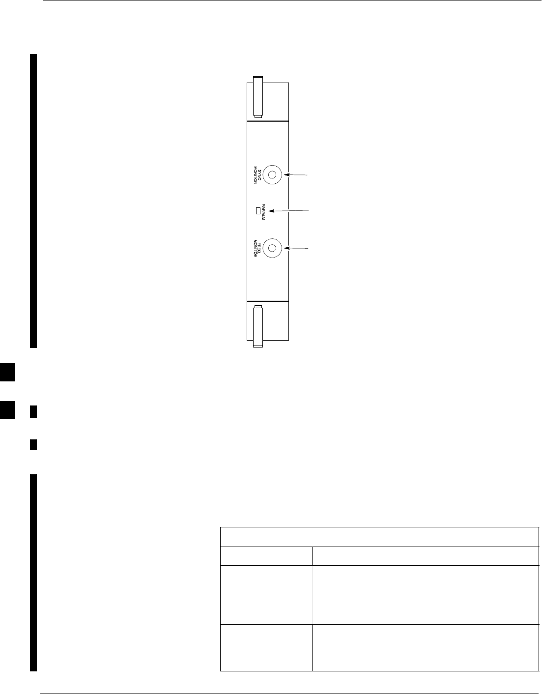
Module Front Panel LED Indicators and Connectors – continued
6-34 1X SC 4812T Lite BTS Optimization/ATP FEB 2005
PRELIMINARY
PWR/ALM
Indicator
FREQ
MONITOR
SYNC
MONITOR
FW00303
Figure 6-2: CSM Front Panel LED and Monitor Ports
GLI3 LED Status Combinations
The GLI3 Card Indicators, Controls, and Connectors are described below
and shown in Figure 6-3.
The Front Panel Indicators and Controls consist of:
SFour LEDs
SOne Pushbutton
ACTIVE LED
Table 6-36: GLI Card ACTIVE LED States
LED State Device Status
Solid GREEN INS_ACTIVE Mode
– This indication means that the GLI has Shelf
Control and is providing control of the
digital interfaces.
OFF Not Active (i.e., INS_STANDBY).
– The Mate GLI is INS_ACTIVE and
operating normally.
6

Module Front Panel LED Indicators and Connectors – continued
FEB 2005 1X SC 4812T Lite BTS Optimization/ATP 6-35
PRELIMINARY
MASTER LED
Table 6-37: GLI Card MASTER LED States
LED State Device Status
Solid GREEN GLI is Master (also referred to as MGLI).
– The GLI Card located in the Top Shelf is
designated by hardware as the
INS_ACTIVE GLI Card.
– The GLI Card located in the Bottom Shelf is
designated by hardware as the
INS_STANDBY GLI Card.
OFF GLI is non-master (i.e., Slave).
ALARM LED
Table 6-38: GLI Card ALARM LED States
LED State Device Status
Slow Flashing
GREEN INS_ACTIVE or INS_STANDBY Mode.
Solid GREEN Turns ON briefly during System Initialization
when the STATUS LED turns OFF.
OFF GLI is operating normally.
STATUS LED
Table 6-39: GLI Card STATUS LED States
LED State Device Status
Slow Flashing
GREEN INS_ACTIVE or INS_STANDBY
Solid GREEN Turns ON briefly during System Initialization
when the ALARM LED turns OFF.
OFF GLI is operating normally.
SPANS LED
Table 6-40: GLI Card STATUS LED States
LED State Device Status
Solid GREEN GLI is operating normally.
Solid YELLOW One or more of the equipped initialized Span
Lines is receiving a Remote Alarm Indication
Signal from the Remote End of the Span Line.
table continued on next page
6

Module Front Panel LED Indicators and Connectors – continued
6-36 1X SC 4812T Lite BTS Optimization/ATP FEB 2005
PRELIMINARY
Table 6-40: GLI Card STATUS LED States
LED State Device Status
Solid RED One or more of the equipped initialized Span
Lines is in Alarm Mode.
OFF GLI is powered down, in Initialization Mode, or
in INS_STANDBY Mode.
GLI3 Pushbutton and
Connectors
Figure 6-3 shows the Front Panel of the GLI3 Card and includes a
description of the components.
RESET Pushbutton
Depressing the RESET Pushbutton causes a partial reset of the CPU and
a reset of all board devices. GLI3 will be placed in the OOS_ROM state
(blue).
MMI Connector
The RS–232MMI Port Connector is intended primarily for development
or factory use but may be used in the field for Debug/Maintenance
purposes.
6
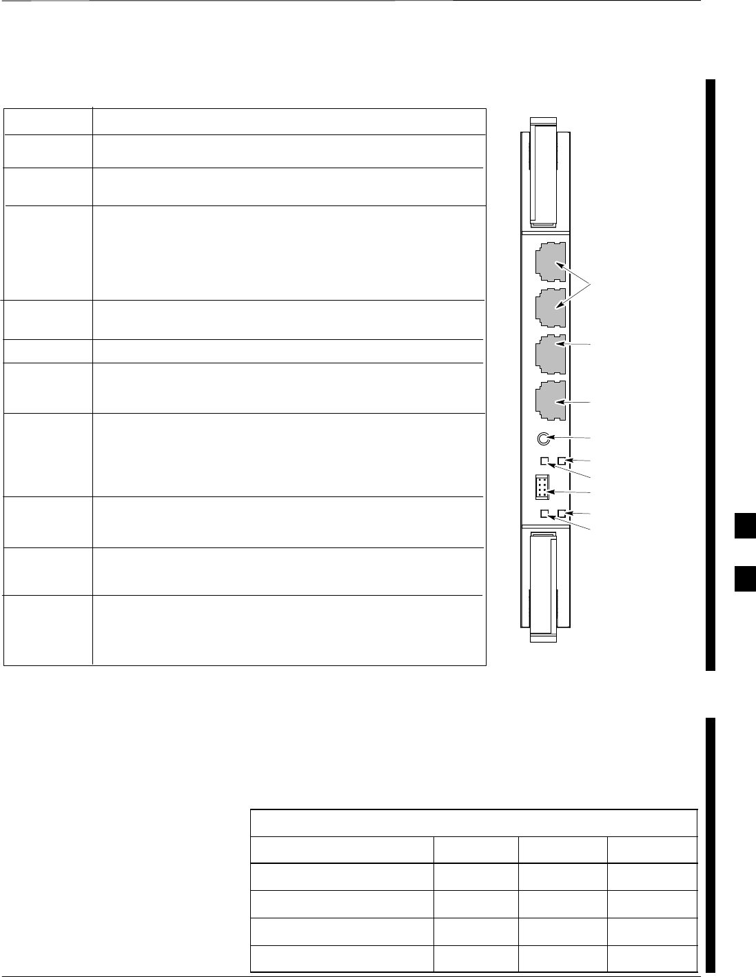
Module Front Panel LED Indicators and Connectors – continued
FEB 2005 1X SC 4812T Lite BTS Optimization/ATP 6-37
PRELIMINARY
STATUS OFF − operating normally.
ON − briefly during powerĆup when the Alarm LED turns OFF.
SLOW GREEN − when the GLI3 is INS (inĆservice).
RESET
ALARM OFF − operating normally.
ON − briefly during powerĆup when the Alarm LED turns OFF.
SLOW GREEN − when the GLI3 is INS (inĆservice).
BPR A
Span
ACTIVE
LED OPERATING STATUS
Pressing and releasing the switch resets all functions on the GLI3.
Shows the operating status of the redundant cards. The redundant
card toggles automatically if the active card is removed or fails.
ON − active card operating normally.
OFF − standby card operating normally.
Connects to either a BPR or Expansion Cage and is wired as an
Ethernet hub.
An RSĆ232, serial, asynchronous communications link for use as
an MMI port. This port supports 300 baud, up to a maximum of
115,200 baud communications.
BPR B
GLI
AUX
Supports the cross−coupled Ethernet circuits to the Mate GLI using a
standard Ethernet straight cable.
Wired as an Ethernet hub for direct connection to a personal computĆ
er with a standard Ethernet cable. It allows connection of an Ethernet
sniffer" when the Ethernet switch is properly configured for port monĆ
itoring. This port may also be connected to the optional Motorola
MOSCAD−L Network Fault Management unit using a Crossover
Ethernet cable.
Connects to either a BPR or Expansion Cage and is wired as an
Ethernet hub.
MMI Port
Reset Switch
Dual 100BASE–T
in a single RJ45
to Redundant
(Mate) GLI3
100BASE–T
Auxiliary Monitor
Port
BPR B AUX RESET
SPAN
ALARM MMI
ACT
STA
100BASE–T to
BTS Packet Router
or Expansion Port
Span (LED)
Alarm (LED)
Active (LED)
Status (LED)
GLIBPR A
ti-CDMA-WP-00064-v01-ildoc-ftw
OFF − card is powered down, in initialization, or in standby.
GREEN − operating normally.
YELLOW − one or more of the equipped initialized spans is receiving
a remote alarm indication signal from the far end.
RED − one or more of the equipped initialized spans is in an alarm
state.
MMI
Figure 6-3: GLI3 Front Panel
BBX LED Status Combinations
PWR/ALM LED
All Broadband Transceiver (BBX) Cards have their own Alarm (Fault)
Detection Circuitry that controls the state of the PWR/ALM LED.
Table 6-41 describes the states of the bi-color PWR/ALM LED.
Table 6-41: BBX Card PWR/ALM LED States
Physical and Alarm State Off Red Green
Microprocessor in Reset ––– Continuous –––
OOS–ROM – No alarm 1.4s ––– 0.2s
OOS–ROM – Alarm ––– 1.4s 0.2s
OOS–RAM – No alarm 0.2s ––– 0.2s
6

Module Front Panel LED Indicators and Connectors – continued
6-38 1X SC 4812T Lite BTS Optimization/ATP FEB 2005
PRELIMINARY
Table 6-41: BBX Card PWR/ALM LED States
Physical and Alarm State GreenRedOff
OOS–RAM – Alarm ––– 0.2s 0.2s
In Service – No alarm ––– ––– Continuous
In Service – Alarm ––– 0.2s 1.4s
ACTIVE LED
Table 6-42 describes the states of the ACTIVE LED:
Table 6-42: BBX Card ACTIVE LED States
Physical and Alarm State Off Red Green
Dekeyed Continuous ––– –––
Keyed ––– ––– Continuous
MCC LED Status Combinations
The Multi-Channel CDMA (MCC–24/MCC–8E/MCC–1X) Card has
Status Indicator LEDs and Connectors as described below. Refer to
Figure 6-4. Note that the figure does not show the connectors; they are
concealed by the removable lens. The location of the LEDs are as
follows:
SPWR/ALM LED is at the top of the card.
SACTIVE LED is at the bottom of the card.
PWR/ALM LED
Table 6-43: MCC Card PWR/ALM LED States
LED State Device Status
Solid RED 1. Briefly lit during System Initialization.
2. Alarm (Fault) Mode.
– An alarm is being reported.
OFF Operating normally.
ACTIVE LED
Table 6-44: MCC Card ACTIVE LED States
LED State Device Status
Solid GREEN Card is code–loaded, enabled, and operating
in INS_ACTIVE Mode, on-line, processing
traffic.
– No alarm present.
Slow Flashing GREEN Card is not code–loaded.
– No alarm present.
6

Module Front Panel LED Indicators and Connectors – continued
FEB 2005 1X SC 4812T Lite BTS Optimization/ATP 6-39
PRELIMINARY
Table 6-44: MCC Card ACTIVE LED States
LED State Device Status
Fast Flashing GREEN Card is code–loaded but not enabled.
– No alarm present.
Solid RED Alarm (Fault) Mode.
– An alarm is being reported.
Alternating
Slow Flashing RED /
Slow Flashing GREEN
The CHI Bus is inactive after System
Initialization.
OFF 1. Card is inactive.
2. Card is off-line.
3. Card is not processing traffic.
Both PWR/ALM and ACTIVE LEDs
Table 6-45: MCC Card PWR/ALM and ACTIVE LED States
LED State Device Status
Solid RED 1. Card is in Reset Mode.
2. The BCP is inactive.
MMI Connectors
RS–232 Port Connector:
This Port Connector (four pin) is intended to be used primarily in
Development and Factory environments, but may be used in the field for
Debugging purposes.
– A Removable Lens covers this Port Connector.
The RJ–14 Ethernet Port Connector:
This Port Connector (eight pin) is intended to be used primarily in the
Development environment, but may be used in the field for High Data
Rate Debugging purposes.
– A Removable Lens covers this Port Connector.
6

Module Front Panel LED Indicators and Connectors – continued
6-40 1X SC 4812T Lite BTS Optimization/ATP FEB 2005
PRELIMINARY
PWR/ALM LED
LENS
(REMOVABLE)
ACTIVE LED
PWR/ALM ACTIVE
LED OPERATING STATUSCOLOR
An alarm is generated in the event of a failure
2) Continuously during fault conditions
ON – 1) Briefly during Power–up
SLOW FLASHING (alternately with green) –
Concentration Highway Interface (CHI) Bus
inactive on Power–up
RED
RED
GREENACTIVE
PWR/ALM OFF – Operating normally
ON – Briefly during Power–up and during
failure conditions
RAPIDLY FLASHING – Card is Code Loaded but
not enabled
ON – Card is Code Loaded and enabled (INS_ACT)
SLOW FLASHING – Card is not Code Loaded
4812ETL0030–1
Figure 6-4: MCC24 and MCC–1X Front Panel LEDs and LED Indications
CLPA LED Status
Combinations
ETIB Board LED for the LPA Module
In the SC 4812T Lite Platform, the CLPA Module does not contain an
LEDs. The LED on the CLPA Fan Module provides visual operational
information for the CLPA Module. Refer to Figure 6-5.
Each LPA Module is provided with a bi–color LED on the ETIB Module
next to the MMI Connector. Refer to Table 6-46.
6
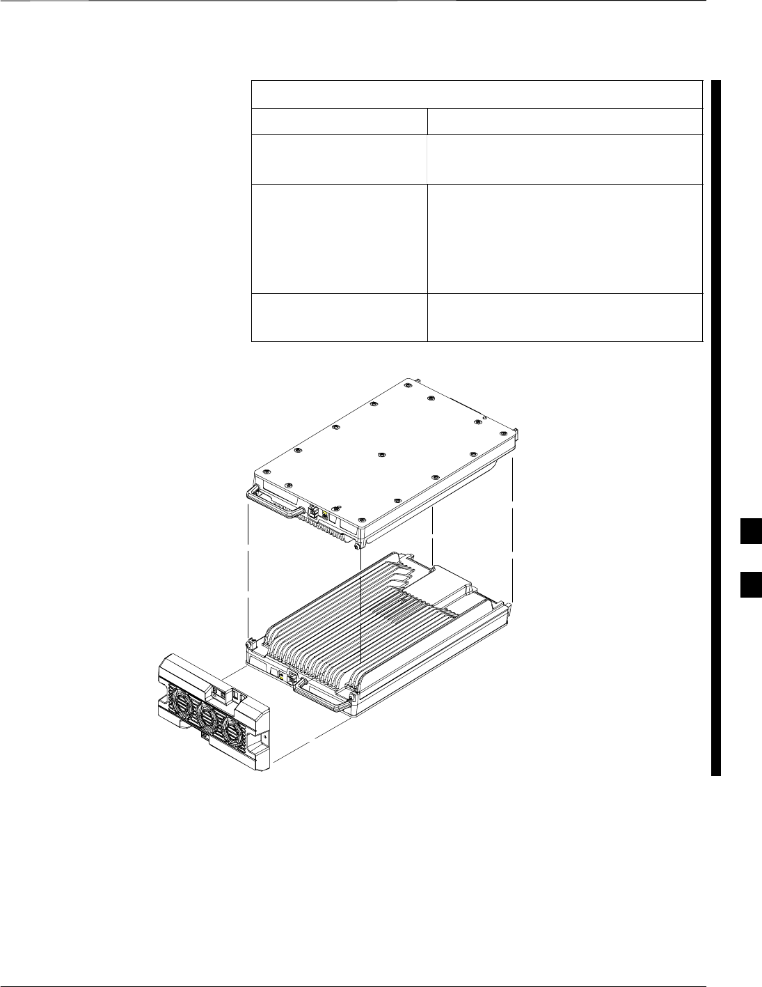
Module Front Panel LED Indicators and Connectors – continued
FEB 2005 1X SC 4812T Lite BTS Optimization/ATP 6-41
PRELIMINARY
Table 6-46: LPA ETIB Module LED
LED State Device Status
Solid GREEN INS_ACTIVE Mode
– No alarm present.
Alternating Flashing
GREEN/ RED INS_ACTIVE Mode
SIf a BBX is keyed, a Low Power
Alarm is present.
SIf a BBX is not keyed, no alarm is
present.
Flashing RED Alarm (Fault) Mode
– An LPA Alarm is being reported.
Figure 6-5: CLPA Module
TOP
CLPA
MODULE
BOTTOM
CLPA
MODULE
FAN
MODULE
6

Troubleshooting: Span Control Link
6-42 1X SC 4812T Lite BTS Optimization/ATP FEB 2005
PRELIMINARY
Span Problems (No Control
Link)
Table 6-47: Control Link Failure Troubleshooting Procedure
nStep Action
1Connect the LMF Computer to the MMI Port on the applicable MGLI3/GLI3 as shown in
Figure 6-6.
2Start an MMI Communication Session with the applicable MGLI3/GLI3 by using the Windows
Desktop Shortcut Icon.
– Refer to Table 3-14.
3Once the connection window opens, press the LMF Computer Enter Key until the GLI3>
Prompt is obtained.
4At the GLI3> Prompt, enter:
config ni current <cr> (equivalent of Span view command)
The system will respond with a display similar to the following:
The frame format in flash is set to use T1_2.
Equalization:
Span A – Default (0–131 feet for T1/J1, 120 Ohm for E1)
Span B – Default (0–131 feet for T1/J1, 120 Ohm for E1)
Span C – Default (0–131 feet for T1/J1, 120 Ohm for E1)
Span D – Default (0–131 feet for T1/J1, 120 Ohm for E1)
Span E – Default (0–131 feet for T1/J1, 120 Ohm for E1)
Span F – Default (0–131 feet for T1/J1, 120 Ohm for E1)
Linkspeed: Default (56K for T1 D4 AMI, 64K otherwise)
Currently, the link is running at the default rate
The actual rate is 0
NOTE
Defaults for Span Equalization are 0–131 feet for T1/J1 Spans and 120 Ohm for E1.
Default Link Speed is 56K for T1 D4 AMI Spans and 64K for all other types.
There is no need to change from defaults unless the OMC–R/CBSC Span Configuration requires it.
5The Span Configurations loaded in the GLI must match those in the OMC–R/CBSC Database for
the BTS.
SIf they do, proceed to Step 6.
SIf they do not, proceed to Table 6-48.
6Repeat Steps 1 through 5 for all remaining GLI Cards.
7If the Span Settings are correct, verify the EDLC Parameters using the show Command.
– Check for any Alarm Conditions that indicate the Span is not operating correctly.
STry looping back the Span Line from the DSX Panel to the MM, and verify that the looped
signal is good.
SListen for a Control Tone on the appropriate Timeslot from the Base Site and MM.
table continued on next page
6
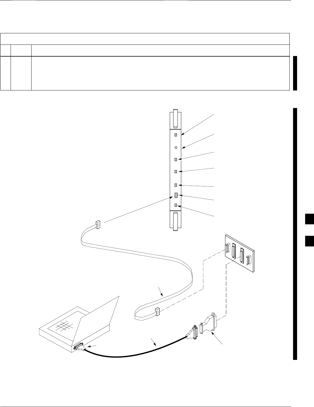
Troubleshooting: Span Control Link – continued
FEB 2005 1X SC 4812T Lite BTS Optimization/ATP 6-43
PRELIMINARY
Table 6-47: Control Link Failure Troubleshooting Procedure
nActionStep
8Exit the GLI MMI Session and HyperTerminal Connection by performing the following actions.
8a Select File from the Connection Window Menu Bar.
8b Select Exit from the Pull–down Menu.
NULL MODEM
BOARD
(TRN9666A)
8–PIN TO 10–PIN
RS–232 CABLE (P/N
30–09786R01)
RS–232 CABLE
8–PIN
LMF
COMPUTER
To MMI Port
DB9–TO–DB25
ADAPTER
COM1
OR
COM2
ACTIVE LED
STATUS LED
ALARM LED
MASTER LED
MMI Port
Connector
STATUS RESET ALARM SPANS MASTER MMI ACTIVE
SPANS LED
RESET
Pushbutton
Figure 6-6: MGLI/GLI Board MMI Connection Detail
6

Troubleshooting: Span Control Link – continued
6-44 1X SC 4812T Lite BTS Optimization/ATP FEB 2005
PRELIMINARY
Set BTS Site Span
Configuration
Perform the following procedure ONLY if Span
Configurations loaded in the MGLI3/GLI3s do not match
those in the OMC–R/CBSC database, AND ONLY when
the exact Configuration Data is available.
Loading incorrect Span Configuration Data will render the
site inoperable.
NOTE
Table 6-48: Set BTS Span Parameter Configuration Procedure
nStep Action
1If not previously done, connect the LMF Computer to the MMI Port on the applicable
MGLI3/GLI3 as shown in Figure 6-6.
2If there is no MMI Communication Session in progress with the applicable MGLI3/GLI3, initiate
one by using the Windows Desktop Shortcut Icon.
– Refer to Table 3-14.
3At the GLI3> Prompt, enter the following command
GLI3>config ni format <option> <cr>
– The terminal will display a response similar to the following:
COMMAND SYNTAX: config ni format option
Next available options:
LIST – option : Span Option
E1_1 : E1_1 – E1 HDB3 CRC4 no TS16
E1_2 : E1_2 – E1 HDB3 no CRC4 no TS16
E1_3 : E1_3 – E1 HDB3 CRC4 TS16
E1_4 : E1_4 – E1 HDB3 no CRC4 TS16
T1_1 : T1_1 – D4, AMI, No ZCS
T1_2 : T1_2 – ESF, B8ZS
J1_1 : J1_1 – ESF, B8ZS (Japan) – Default
J1_2 : J1_2 – ESF, B8ZS
T1_3 : T1_3 – D4, AMI, ZCS>
NOTE
With this command, all active (in–use) Spans will be set to the same format.
table continued on next page
6

Troubleshooting: Span Control Link – continued
FEB 2005 1X SC 4812T Lite BTS Optimization/ATP 6-45
PRELIMINARY
Table 6-48: Set BTS Span Parameter Configuration Procedure
nActionStep
4To set or change the Span Type, enter the correct option from the list at the Entry Prompt (>), as
shown in the following example.
> T1_2 <cr>
– An acknowledgement similar to the following will be displayed:
The value has been programmed. It will take effect after the next reset.
GLI3>
NOTE
The entry is case–sensitive and must be typed exactly as it appears in the list.
– If the entry is typed incorrectly, a response similar to the following will be displayed:
CP: Invalid command
GLI3>
5If the current MGLI/GLI Span Rate must be changed, enter the following MMI Command:
config ni Link Speed <cr>
– The terminal will display a response similar to the following:
Next available options:
LIST – Link Speed : Span Linkspeed
56K : 56K (default for T1_1 and T1_3 systems)
64K : 64K (default for all other Span Configurations)
>
NOTE
With this command, all active (in–use) Spans will be set to the same Link Speed.
6To set or change the Span Link Speed, enter the required option from the list at the Entry Prompt
(>), as shown in the following example:
> 64K <cr>
– An acknowledgement similar to the following will be displayed:
The value has been programmed. It will take effect after the next reset.
GLI3>
NOTE
The entry is case–sensitive and must be typed exactly as it appears in the list.
– If the entry is typed incorrectly, a response similar to the following will be displayed:
CP: Invalid command
GLI3>
table continued on next page
6

Troubleshooting: Span Control Link – continued
6-46 1X SC 4812T Lite BTS Optimization/ATP FEB 2005
PRELIMINARY
Table 6-48: Set BTS Span Parameter Configuration Procedure
nActionStep
7If the Span Equalization must be changed, enter the following MMI Command:
config ni equal <cr>
– The terminal will display a response similar to the following:
COMMAND SYNTAX: config ni equal Span equal
Next available options:
LIST – Span : Span
a : Span A
b : Span B
c : Span C
d : Span D
e : Span E
f : Span F
>
8At the Entry Prompt (>), enter the designator from the list for the Span to be changed as shown in
the following example:
> a <cr>
– The terminal will display a response similar to the following:
COMMAND SYNTAX: config ni equal a equal
Next available options:
LIST – equal : Span Equalization
0 : 0–131 feet (default for T1/J1)
1 : 132–262 feet
2 : 263–393 feet
3 : 394–524 feet
4 : 525–655 feet
5 : LONG HAUL
6 : 75 OHM
7 : 120 OHM (default for E1)
>
9At the Entry Prompt (>), enter the code for the required equalization from the list as shown in the
following example:
> 0 <cr>
– The terminal will display a response similar to the following:
> 0
The value has been programmed. It will take effect after the next reset.
GLI3>
10 Repeat Step 7 through Step 9 for each in–use Span.
table continued on next page
6

Troubleshooting: Span Control Link – continued
FEB 2005 1X SC 4812T Lite BTS Optimization/ATP 6-47
PRELIMINARY
Table 6-48: Set BTS Span Parameter Configuration Procedure
nActionStep
11 Press the RESET Button on the MGLI3/GLI3 for changes to take effect.
* IMPORTANT
After executing the config ni format, config ni Link Speed, and/or config ni equal
commands, the affected MGLI/GLI Card MUST be reset and reloaded for changes to take effect.
Although defaults are shown, always consult the Site Documentation for Span Type and Link
Speed used at the site.
12 Once the MGLI/GLI has reset, execute the following command to verify Span Settings are as
required:
config ni current <cr> (equivalent of Span view command)
– The system will respond with a display similar to the following:
The frame format in flash is set to use T1_2.
Equalization:
Span A – 0–131 feet
Span B – 0–131 feet
Span C – Default (0–131 feet for T1/J1, 120 Ohm for E1)
Span D – Default (0–131 feet for T1/J1, 120 Ohm for E1)
Span E – Default (0–131 feet for T1/J1, 120 Ohm for E1)
Span F – Default (0–131 feet for T1/J1, 120 Ohm for E1)
Linkspeed: 64K
Currently, the link is running at 64K
The actual rate is 0
SIf the Span Configuration is correct, return to Step 6 of Table 6-47.
SIf the Span Configuration is not correct, proceed to Step 13.
13 Perform the applicable step from this table to change it.
14 Repeat Step 11 and Step 12 to verify required changes have been programmed.
6

Troubleshooting: Span Control Link – continued
6-48 1X SC 4812T Lite BTS Optimization/ATP FEB 2005
PRELIMINARY
Notes
6

FEB 2005 1X SC 4812T Lite BTS Optimization/ATP
PRELIMINARY
Appendix A: Data Sheets
Appendix Content
Optimization (Pre–ATP) Data Sheets A-1 . . . . . . . . . . . . . . . . . . . . . . . . . . . . . . . . .
Verification of Test Equipment Used A-1 . . . . . . . . . . . . . . . . . . . . . . . . . . .
Site Checklist A-2 . . . . . . . . . . . . . . . . . . . . . . . . . . . . . . . . . . . . . . . . . . . . .
Preliminary Operations A-2 . . . . . . . . . . . . . . . . . . . . . . . . . . . . . . . . . . . . .
Pre–Power and Initial Power Tests A-3 . . . . . . . . . . . . . . . . . . . . . . . . . . . .
General Optimization Checklist A-4 . . . . . . . . . . . . . . . . . . . . . . . . . . . . . .
GPS Receiver Operation A-5 . . . . . . . . . . . . . . . . . . . . . . . . . . . . . . . . . . . .
LPA IM Reduction A-6 . . . . . . . . . . . . . . . . . . . . . . . . . . . . . . . . . . . . . . . . .
TX Bay Level Offset / Power Output Verification for 3–Sector
Configurations A-7 . . . . . . . . . . . . . . . . . . . . . . . . . . . . . . . . . . . . . . . . . . .
TX Antenna VSWR A-9 . . . . . . . . . . . . . . . . . . . . . . . . . . . . . . . . . . . . . . . .
RX Antenna VSWR A-9 . . . . . . . . . . . . . . . . . . . . . . . . . . . . . . . . . . . . . . . .
Alarm Verification A-10 . . . . . . . . . . . . . . . . . . . . . . . . . . . . . . . . . . . . . . . . .
Site Serial Number Check List A-11 . . . . . . . . . . . . . . . . . . . . . . . . . . . . . . . . . . . . . .
SCCP Cage A-11 . . . . . . . . . . . . . . . . . . . . . . . . . . . . . . . . . . . . . . . . . . . . . .
LPA Modules A-12 . . . . . . . . . . . . . . . . . . . . . . . . . . . . . . . . . . . . . . . . . . . . .
A

Table of Contents – continued
1X SC 4812T Lite BTS Optimization/ATP FEB 2005
PRELIMINARY
Notes
A

Optimization (Pre–ATP) Data Sheets
FEB 2005 1X SC 4812T Lite BTS Optimization/ATP A-1
PRELIMINARY
Verification of Test Equipment
Used
Table A-1: Verification of Test Equipment Used
Manufacturer Model Serial Number
Comments:________________________________________________________
__________________________________________________________________
A

Optimization (Pre–ATP) Data Sheets – continued
A-2 1X SC 4812T Lite BTS Optimization/ATP FEB 2005
PRELIMINARY
Site Checklist
Table A-2: Site Checklist
OK Parameter Specification Comments
−Deliveries Per established
procedures
−Floor Plan Verified
−
−
−
Inter Frame Cables:
Ethernet
Frame Ground
Power
Per procedure
Per procedure
Per procedure
−
−
−
Factory Data:
BBX
Test Panel
RFDS
Per procedure
Per procedure
Per procedure
−Site Temperature
−Dress Covers/Brackets
Preliminary Operations
Table A-3: Preliminary Operations
OK Parameter Specification Comments
−Frame ID DIP Switches Per Site
Equipage
−Ethernet LAN
Verification Verified per
procedure
Comments:_________________________________________________________
A

Optimization (Pre–ATP) Data Sheets – continued
FEB 2005 1X SC 4812T Lite BTS Optimization/ATP A-3
PRELIMINARY
Pre–Power and Initial Power
Tests
Table A-4: Pre–power Checklist
OK Parameter Specification Comments
−Pre–Power–up Tests Table 2-2
−
−
−
−
−
−
−
−
−
−
Internal Cables:
Span
CSM
Power
Ethernet Connectors:
LAN A Ohms
LAN B Ohms
LAN A Shield
LAN B Shield
LAN A IN & OUT
Terminators
LAN B IN & OUT
Terminators
Ethernet Boots
Verified
Verified
Verified
Verified
Verified
Installed
Installed
Isolated
Isolated
Installed
−Air Impedance Cage (single cage) Installed
−Initial Power–up Tests Table 2-5
−
−
Frame Fans
LEDs
Operational
Illuminated
Comments:_________________________________________________________
A

Optimization (Pre–ATP) Data Sheets – continued
A-4 1X SC 4812T Lite BTS Optimization/ATP FEB 2005
PRELIMINARY
General Optimization Checklist
Table A-5: General Optimization Checklist
OK Parameter Specification Comments
−
−
−
Preparing the LMF
Load LMF Software
Create site–specific BTS directory
Create HyperTerminal Connection
Table 3-2
Table 3-3
Table 3-4
−
−
−
−
LMF–to–BTS Connection
Verify GLI2 Ethernet Address Settings
Ping LAN A
Ping LAN B
Table 3-6
Table 6-4
Table 3-15
Table 3-15
−
−
−
−
−
−
−
−
−
Verify ROM Code Loads for Software
Release
Download/Enable MGLI2
Download/Enable GLI2
Set Site Span Configuration
Set CSM Clock Source
Enable CSM Cards
Download/Enable MCC Cards (24/8E/1X)
Download BBX Cards (2 or 1X)
Program TSU NAM
Table 3-16
Table 3-17
Table 3-17
Table 6-47
Table 3-19
Table 3-20
Table 3-18
Table 3-18
Table 3-52
−
−
Test Set Calibration
Test Cable Calibration
Table 3-36
Table 3-32
Comments:_________________________________________________________
A

Optimization (Pre–ATP) Data Sheets – continued
FEB 2005 1X SC 4812T Lite BTS Optimization/ATP A-5
PRELIMINARY
GPS Receiver Operation
Table A-6: GPS Receiver Operation
OK Parameter Specification Comments
−GPS Receiver Control Task State:
tracking satellites
Verify parameter
−Initial Position Accuracy: Verify:
Estimated or
Surveyed
−Current Position:
lat
lon
height
RECORD in
msec and cm.
Also convert to
deg min sec.
−Current Position: satellites tracked
Estimated:
(>4) satellites tracked,(>4) satellites visible
Surveyed:
(>1) satellite tracked,(>4) satellites visible
Verify parameter
as appropriate
−GPS Receiver Status:Current Dilution of
Precision
(PDOP or HDOP): (<30)
Verify parameter
−Current Reference Source:
Number: 0; Status: Good; Valid: Yes Verify parameter
Comments:_________________________________________________________
A

Optimization (Pre–ATP) Data Sheets – continued
A-6 1X SC 4812T Lite BTS Optimization/ATP FEB 2005
PRELIMINARY
LPA IM Reduction
Table A-7: LPA IM Reduction
Parameter
Carrier
OK LPA
#2:1
3–Sector BP
3–Sector Specification Comments
−1A C1 C1 No Alarms
−1B C1 C1 No Alarms
−1C C1 C1 No Alarms
−1D C1 C1 No Alarms
−3A C2 C2 No Alarms
−3B C2 C2 No Alarms
−3C C2 C2 No Alarms
−3D C2 C2 No Alarms
Comments:_________________________________________________________
A

Optimization (Pre–ATP) Data Sheets – continued
FEB 2005 1X SC 4812T Lite BTS Optimization/ATP A-7
PRELIMINARY
TX Bay Level Offset / Power
Output Verification for
3–Sector Configurations
One Carrier and Two Carrier Non–adjacent Channels
Table A-8: TX BLO Calibration (Three Sector: One Carrier and Two Carrier Non–adjacent Channels)
OK Parameter Specification Comments
−BBX2–1, ANT–1A = ______dB
BBX2–r, ANT–1A = ______dB
−Calibrate Carrier 1 TX Bay Level Offset = 45 dB
(+5 dB) prior to Calibration
BBX2–2, ANT–2A = ______dB
BBX2–r, ANT–2A = ______dB
−BBX2–3, ANT–3A = ______dB
BBX2–r, ANT–3A = ______dB
−BBX2–4, ANT–1B = ______dB
BBX2–r, ANT–1B = ______dB
−Calibrate Carrier 2 TX Bay Level Offset = 45 dB
(+5 dB) prior to Calibration
BBX2–5, ANT–2B = ______dB
BBX2–r, ANT–2B = ______dB
−BBX2–6, ANT–3B = ______dB
BBX2–r, ANT–3B = ______dB
−BBX2–1, ANT–1A = ______dB
BBX2–r, ANT–1A = ______dB
−Calibration Audit
Carrier 1 0 dB (+0.5 dB) for Gain Set
Resolution Post–Calibration
BBX2–2, ANT–2A = ______dB
BBX2–r, ANT–2A = ______dB
−BBX2–3, ANT–3A = ______dB
BBX2–r, ANT–3A = ______dB
−BBX2–4, ANT–1B = ______dB
BBX2–r, ANT–1B = ______dB
−Calibration Audit
Carrier 2 0 dB (+0.5 dB) for Gain Set
Resolution Post–Calibration
BBX2–5, ANT–2B = ______dB
BBX2–r, ANT–2B = ______dB
−BBX2–6, ANT–3B = ______dB
BBX2–r, ANT–3B = ______dB
Comments:________________________________________________________
__________________________________________________________________
A

Optimization (Pre–ATP) Data Sheets – continued
A-8 1X SC 4812T Lite BTS Optimization/ATP FEB 2005
PRELIMINARY
Two Carrier Adjacent Channel
Table A-9: TX Bay Level Offset Calibration (Three Sector: Two Carrier Adjacent Channels)
OK Parameter Specification Comments
−BBX2–1, ANT–1A = ______dB
BBX2–r, ANT–1A = ______dB
−Calibrate Carrier 1 TX Bay Level Offset = 45 dB (typical),
38 dB (minimum) prior to Calibration
BBX2–2, ANT–2A = ______dB
BBX2–r, ANT–2A = ______dB
−BBX2–3, ANT–3A = ______dB
BBX2–r, ANT–3A = ______dB
−BBX2–4, ANT–1B = ______dB
BBX2–r, ANT–1B = ______dB
−Calibrate Carrier 2 TX Bay Level Offset = 45 dB (typical),
38 dB (minimum) prior to Calibration
BBX2–5, ANT–2B = ______dB
BBX2–r, ANT–2B = ______dB
−BBX2–6, ANT–3B = ______dB
BBX2–r, ANT–3B = ______dB
−BBX2–1, ANT–1A = ______dB
BBX2–r, ANT–1A = ______dB
−Calibration Audit
Carrier 1 0 dB (+0.5 dB) for Gain Set Resolution
Post–Calibration
BBX2–2, ANT–2A = ______dB
BBX2–r, ANT–2A = ______dB
−BBX2–3, ANT–3A = ______dB
BBX2–r, ANT–3A = ______dB
−BBX2–4, ANT–1B = ______dB
BBX2–r, ANT–1B = ______dB
−Calibration Audit
Carrier 2 0 dB (+0.5 dB) for Gain Set Resolution
Post–Calibration
BBX2–5, ANT–2B = ______dB
BBX2–r, ANT–2B = ______dB
−BBX2–6, ANT–3B = ______dB
BBX2–r, ANT–3B = ______dB
Comments:________________________________________________________
__________________________________________________________________
A

Optimization (Pre–ATP) Data Sheets – continued
FEB 2005 1X SC 4812T Lite BTS Optimization/ATP A-9
PRELIMINARY
TX Antenna VSWR
Table A-10: TX Antenna VSWR
OK Parameter Specification Data
−VSWR –
Antenna 1A < (1.5 : 1)
−VSWR –
Antenna 2A < (1.5 : 1)
−VSWR –
Antenna 3A < (1.5 : 1)
−VSWR –
Antenna 1B < (1.5 : 1)
−VSWR –
Antenna 2B < (1.5 : 1)
−VSWR –
Antenna 3B < (1.5 : 1)
Comments:________________________________________________________
__________________________________________________________________
RX Antenna VSWR
Table A-11: RX Antenna VSWR
OK Parameter Specification Data
−VSWR –
Antenna 1A < (1.5 : 1)
−VSWR –
Antenna 2A < (1.5 : 1)
−VSWR –
Antenna 3A < (1.5 : 1)
−VSWR –
Antenna 1B < (1.5 : 1)
−VSWR –
Antenna 2B < (1.5 : 1)
−VSWR –
Antenna 3B < (1.5 : 1)
Comments:_________________________________________________________
__________________________________________________________________
A

Optimization (Pre–ATP) Data Sheets – continued
A-10 1X SC 4812T Lite BTS Optimization/ATP FEB 2005
PRELIMINARY
Alarm Verification
Table A-12: CDI Alarm Input Verification
OK Parameter Specification Data
−Verify CDI Alarm
Input Operation. BTS Relay #XX –
Contact Alarm Sets/Clears
Comments:_________________________________________________________
A

Site Serial Number Check List
FEB 2005 1X SC 4812T Lite BTS Optimization/ATP A-11
PRELIMINARY
Date Site
SCCP Cage
For BBX Cards and MCC Cards, enter the type as well as
Serial Number; for example, BBX2, BBX–1X, MCC8,
MCC24, MCC–1X.
NOTE
Site I/O A
Site I/O B
SCCP Cage
CSM–1
CSM–2
HSO
CCD–1
CCD–2
AMR–1
AMR–2
MPC–1
MPC–2
Fan–1
Fan–2
GLI2–1
GLI2–2
GLI2–2
BBX–1
BBX–2
BBX–3
BBX–4
BBX–5
BBX–6
BBX–R1
MCC–1
MCC–2
MCC–3
A

Site Serial Number Check List – continued
A-12 1X SC 4812T Lite BTS Optimization/ATP FEB 2005
PRELIMINARY
MCC–4
CIO
SWITCH
PS–1
PS–2
LPA Modules
PA 1A
PA 1B
PA 1C
PA 1D
PA 3A
PA 3B
PA 3C
PA 3D
A

FEB 2005 1X SC 4812T Lite BTS Optimization/ATP
PRELIMINARY
Appendix B: PN Offset/I & Q Offset Register Programming Information
Appendix Content
PN Offset Programming Information B-1 . . . . . . . . . . . . . . . . . . . . . . . . . . . . . . . . .
PN Offset Background B-1 . . . . . . . . . . . . . . . . . . . . . . . . . . . . . . . . . . . . . .
PN Offset Usage B-1 . . . . . . . . . . . . . . . . . . . . . . . . . . . . . . . . . . . . . . . . . .
B

Table of Contents – continued
1X SC 4812T Lite BTS Optimization/ATP FEB 2005
PRELIMINARY
Notes
B

PN Offset Programming Information
FEB 2005 1X SC 4812T Lite BTS Optimization/ATP B-1
PRELIMINARY
PN Offset Background
All Channel Elements transmitted from a BTS in a specific 1.25 MHz
CDMA Channel are orthogonally spread by 1 of 64 possible Walsh Code
Functions; additionally, they are also spread by a Quadrature Pair of PN
Sequences unique to each sector.
Overall, the mobile uses this to differentiate multiple signals transmitted
from the same BTS (and surrounding BTS) Sectors, and to synchronize
to the next strongest sector.
The PN Offset per Sector is stored on the BBX Cards, where the
corresponding I and Q Registers reside.
The PN Offset Values are determined by BTS Sector (Antenna) based on
the applicable CDF Data Field Content. A breakdown of this
information is found in Table B-1.
PN Offset Usage
There are three basic RF Chip Delays currently in use. It is important to
determine which RF Chip Delay is valid to be able to test the BTS
Functionality. This can be done by ascertaining if the CDF FineTxAdj
Value was set to “on” when the MCC was downloaded with “image
data”.
The FineTxAdj Value is used to compensate for the Processing Delay
(approximately 20 mS) in the BTS using any type of mobile meeting
IS–97 Specifications.
Observe the following guidelines:
SIf the FineTxAdj Value in the CDF is 101 (65 HEX), the FineTxAdj
has not been set. The I and Q Values from the 0 Chip Delay Column
of Table B-1 MUST be used.
If the FineTxAdj Value in the CDF File is 213 (D5 HEX), FineTxAdj
has been set for the 14 Chip Delay column of Table B-1.
SIf the FineTxAdj value in the CDF File is 197 (C5 HEX), FineTxAdj
has been set for the 13Chip Delay column of Table B-1.
CDF File I and Q Values can be represented in DECIMAL
or HEX.
If using HEX, add 0x before the HEX Value.
If necessary, convert HEX values in Table B-1 to decimal
before comparing them to CDF File I and Q Value
Assignments.
NOTE
– If a Qualcomm Mobile is used, select I and Q Values from the
13–Chip Delay column of Table B-1.
– If a mobile is used that does not have the “One Chip Offset”
problem (any mobile meeting the IS–97 Specification), select from
the 14–Chip Delay column of Table B-1.
B

PN Offset Programming Information – continued
B-2 1X SC 4812T Lite BTS Optimization/ATP FEB 2005
PRELIMINARY
If the wrong I and Q Values are used with the wrong
FineTxAdj Parameter, System Timing problems will
occur.
This will cause the energy transmitted to be “smeared”
over several Walsh Codes (instead of the single Walsh
Code that it was assigned to), causing erratic operation.
Evidence of Smearing is usually identified by Walsh
Channels not at correct levels or being present when not
selected in the Code Domain Power Test.
NOTE
B

PN Offset Programming Information – continued
FEB 2005 1X SC 4812T Lite BTS Optimization/ATP B-3
PRELIMINARY
Table B-1: PnMaskI and PnMaskQ Values for PilotPn
14–Chip Delay 13–Chip Delay 0–Chip Delay
Pilot I Q I Q I Q I Q I Q I Q
PN (Dec.) (Hex.) (Dec.) (Hex.) (Dec.) (Hex.)
0 17523 23459 4473 5BA3 29673 25581 73E9 63ED 4096 4096 1000 1000
1 32292 32589 7E24 7F4D 16146 29082 3F12 719A 9167 1571 23CF 0623
2 4700 17398 125C 43F6 2350 8699 092E 21FB 22417 7484 5791 1D3C
3 14406 26333 3846 66DD 7203 32082 1C23 7D52 966 6319 03C6 18AF
4 14899 4011 3A33 0FAB 19657 18921 4CC9 49E9 14189 2447 376D 098F
5 17025 2256 4281 08D0 28816 1128 7090 0468 29150 24441 71DE 5F79
6 14745 18651 3999 48DB 19740 27217 4D1C 6A51 18245 27351 4745 6AD7
7 2783 1094 0ADF 0446 21695 547 54BF 0223 1716 23613 06B4 5C3D
8 5832 21202 16C8 52D2 2916 10601 0B64 2969 11915 29008 2E8B 7150
9 12407 13841 3077 3611 18923 21812 49EB 5534 20981 5643 51F5 160B
10 31295 31767 7A3F 7C17 27855 28727 6CCF 7037 24694 28085 6076 6DB5
11 7581 18890 1D9D 49CA 24350 9445 5F1E 24E5 11865 18200 2E59 4718
12 18523 30999 485B 7917 30205 29367 75FD 72B7 6385 21138 18F1 5292
13 29920 22420 74E0 5794 14960 11210 3A70 2BCA 27896 21937 6CF8 55B1
14 25184 20168 6260 4EC8 12592 10084 3130 2764 25240 25222 6298 6286
15 26282 12354 66AA 3042 13141 6177 3355 1821 30877 109 789D 006D
16 30623 11187 779F 2BB3 27167 23525 6A1F 5BE5 30618 6028 779A 178C
17 15540 11834 3CB4 2E3A 7770 5917 1E5A 171D 26373 22034 6705 5612
18 23026 10395 59F2 289B 11513 23153 2CF9 5A71 314 15069 013A 3ADD
19 20019 28035 4E33 6D83 30409 30973 76C9 78FD 17518 4671 446E 123F
20 4050 27399 0FD2 6B07 2025 31679 07E9 7BBF 21927 30434 55A7 76E2
21 1557 22087 0615 5647 21210 25887 52DA 651F 2245 11615 08C5 2D5F
22 30262 2077 7636 081D 15131 18994 3B1B 4A32 18105 19838 46B9 4D7E
23 18000 13758 4650 35BE 9000 6879 2328 1ADF 8792 14713 2258 3979
24 20056 11778 4E58 2E02 10028 5889 272C 1701 21440 241 53C0 00F1
25 12143 3543 2F6F 0DD7 18023 18647 4667 48D7 15493 24083 3C85 5E13
26 17437 7184 441D 1C10 29662 3592 73DE 0E08 26677 7621 6835 1DC5
27 17438 2362 441E 093A 8719 1181 220F 049D 11299 19144 2C23 4AC8
28 5102 25840 13EE 64F0 2551 12920 09F7 3278 12081 1047 2F31 0417
29 9302 12177 2456 2F91 4651 23028 122B 59F4 23833 26152 5D19 6628
30 17154 10402 4302 28A2 8577 5201 2181 1451 20281 22402 4F39 5782
31 5198 1917 144E 077D 2599 19842 0A27 4D82 10676 21255 29B4 5307
32 4606 17708 11FE 452C 2303 8854 08FF 2296 16981 30179 4255 75E3
33 24804 10630 60E4 2986 12402 5315 3072 14C3 31964 7408 7CDC 1CF0
34 17180 6812 431C 1A9C 8590 3406 218E 0D4E 26913 115 6921 0073
35 10507 14350 290B 380E 17749 7175 4555 1C07 14080 1591 3700 0637
36 10157 10999 27AD 2AF7 16902 23367 4206 5B47 23842 1006 5D22 03EE
37 23850 25003 5D2A 61AB 11925 32489 2E95 7EE9 27197 32263 6A3D 7E07
38 31425 2652 7AC1 0A5C 27824 1326 6CB0 052E 22933 1332 5995 0534
39 4075 19898 0FEB 4DBA 22053 9949 5625 26DD 30220 12636 760C 315C
40 10030 2010 272E 07DA 5015 1005 1397 03ED 12443 4099 309B 1003
41 16984 25936 4258 6550 8492 12968 212C 32A8 19854 386 4D8E 0182
42 14225 28531 3791 6F73 18968 31109 4A18 7985 14842 29231 39FA 722F
43 26519 11952 6797 2EB0 25115 5976 621B 1758 15006 25711 3A9E 646F
44 27775 31947 6C7F 7CCB 26607 28761 67EF 7059 702 10913 02BE 2AA1
45 30100 25589 7594 63F5 15050 32710 3ACA 7FC6 21373 8132 537D 1FC4
46 7922 11345 1EF2 2C51 3961 22548 0F79 5814 23874 20844 5D42 516C
47 14199 28198 3777 6E26 19051 14099 4A6B 3713 3468 13150 0D8C 335E
48 17637 13947 44E5 367B 29602 21761 73A2 5501 31323 18184 7A5B 4708
49 23081 8462 5A29 210E 31940 4231 7CC4 1087 29266 19066 7252 4A7A
50 5099 9595 13EB 257B 22565 23681 5825 5C81 16554 29963 40AA 750B
. . . continued on next page
B

PN Offset Programming Information – continued
B-4 1X SC 4812T Lite BTS Optimization/ATP FEB 2005
PRELIMINARY
Table B-1: PnMaskI and PnMaskQ Values for PilotPn
14–Chip Delay 13–Chip Delay 0–Chip Delay
Pilot I Q I Q I Q I Q I Q I Q
PN (Dec.) (Hex.) (Dec.) (Hex.) (Dec.) (Hex.)
51 32743 4670 7FE7 123E 28195 2335 6E23 091F 22575 6605 582F 19CD
52 7114 14672 1BCA 3950 3557 7336 0DE5 1CA8 31456 29417 7AE0 72E9
53 7699 29415 1E13 72E7 24281 30543 5ED9 774F 8148 22993 1FD4 59D1
54 19339 20610 4B8B 5082 29717 10305 7415 2841 19043 27657 4A63 6C09
55 28212 6479 6E34 194F 14106 17051 371A 429B 25438 5468 635E 155C
56 29587 10957 7393 2ACD 26649 23386 6819 5B5A 10938 8821 2ABA 2275
57 19715 18426 4D03 47FA 30545 9213 7751 23FD 2311 20773 0907 5125
58 14901 22726 3A35 58C6 19658 11363 4CCA 2C63 7392 4920 1CE0 1338
59 20160 5247 4EC0 147F 10080 17411 2760 4403 30714 5756 77FA 167C
60 22249 29953 56E9 7501 31396 29884 7AA4 74BC 180 28088 00B4 6DB8
61 26582 5796 67D6 16A4 13291 2898 33EB 0B52 8948 740 22F4 02E4
62 7153 16829 1BF1 41BD 23592 28386 5C28 6EE2 16432 23397 4030 5B65
63 15127 4528 3B17 11B0 19547 2264 4C5B 08D8 9622 19492 2596 4C24
64 15274 5415 3BAA 1527 7637 17583 1DD5 44AF 7524 26451 1D64 6753
65 23149 10294 5A6D 2836 31974 5147 7CE6 141B 1443 30666 05A3 77CA
66 16340 17046 3FD4 4296 8170 8523 1FEA 214B 1810 15088 0712 3AF0
67 27052 7846 69AC 1EA6 13526 3923 34D6 0F53 6941 26131 1B1D 6613
68 13519 10762 34CF 2A0A 19383 5381 4BB7 1505 3238 15969 0CA6 3E61
69 10620 13814 297C 35F6 5310 6907 14BE 1AFB 8141 24101 1FCD 5E25
70 15978 16854 3E6A 41D6 7989 8427 1F35 20EB 10408 12762 28A8 31DA
71 27966 795 6D3E 031B 13983 20401 369F 4FB1 18826 19997 498A 4E1D
72 12479 9774 30BF 262E 18831 4887 498F 1317 22705 22971 58B1 59BB
73 1536 24291 0600 5EE3 768 24909 0300 614D 3879 12560 0F27 3110
74 3199 3172 0C7F 0C64 22511 1586 57EF 0632 21359 31213 536F 79ED
75 4549 2229 11C5 08B5 22834 19046 5932 4A66 30853 18780 7885 495C
76 17888 21283 45E0 5323 8944 26541 22F0 67AD 18078 16353 469E 3FE1
77 13117 16905 333D 4209 18510 28472 484E 6F38 15910 12055 3E26 2F17
78 7506 7062 1D52 1B96 3753 3531 0EA9 0DCB 20989 30396 51FD 76BC
79 27626 7532 6BEA 1D6C 13813 3766 35F5 0EB6 28810 24388 708A 5F44
80 31109 25575 7985 63E7 27922 32719 6D12 7FCF 30759 1555 7827 0613
81 29755 14244 743B 37A4 27597 7122 6BCD 1BD2 18899 13316 49D3 3404
82 26711 28053 6857 6D95 26107 30966 65FB 78F6 7739 31073 1E3B 7961
83 20397 30408 4FAD 76C8 30214 15204 7606 3B64 6279 6187 1887 182B
84 18608 5094 48B0 13E6 9304 2547 2458 09F3 9968 21644 26F0 548C
85 7391 16222 1CDF 3F5E 24511 8111 5FBF 1FAF 8571 9289 217B 2449
86 23168 7159 5A80 1BF7 11584 17351 2D40 43C7 4143 4624 102F 1210
87 23466 174 5BAA 00AE 11733 87 2DD5 0057 19637 467 4CB5 01D3
88 15932 25530 3E3C 63BA 7966 12765 1F1E 31DD 11867 18133 2E5B 46D5
89 25798 2320 64C6 0910 12899 1160 3263 0488 7374 1532 1CCE 05FC
90 28134 23113 6DE6 5A49 14067 25368 36F3 6318 10423 1457 28B7 05B1
91 28024 23985 6D78 5DB1 14012 24804 36BC 60E4 9984 9197 2700 23ED
92 6335 2604 18BF 0A2C 23951 1302 5D8F 0516 7445 13451 1D15 348B
93 21508 1826 5404 0722 10754 913 2A02 0391 4133 25785 1025 64B9
94 26338 30853 66E2 7885 13169 29310 3371 727E 22646 4087 5876 0FF7
95 17186 15699 4322 3D53 8593 20629 2191 5095 15466 31190 3C6A 79D6
96 22462 2589 57BE 0A1D 11231 19250 2BDF 4B32 2164 8383 0874 20BF
97 3908 25000 0F44 61A8 1954 12500 07A2 30D4 16380 12995 3FFC 32C3
98 25390 18163 632E 46F3 12695 27973 3197 6D45 15008 27438 3AA0 6B2E
99 27891 12555 6CF3 310B 26537 22201 67A9 56B9 31755 9297 7C0B 2451
100 9620 8670 2594 21DE 4810 4335 12CA 10EF 31636 1676 7B94 068C
. . . continued on next page
B

PN Offset Programming Information – continued
FEB 2005 1X SC 4812T Lite BTS Optimization/ATP B-5
PRELIMINARY
Table B-1: PnMaskI and PnMaskQ Values for PilotPn
14–Chip Delay 13–Chip Delay 0–Chip Delay
Pilot I Q I Q I Q I Q I Q I Q
PN (Dec.) (Hex.) (Dec.) (Hex.) (Dec.) (Hex.)
101 6491 1290 195B 050A 23933 645 5D7D 0285 25414 12596 6346 3134
102 16876 4407 41EC 1137 8438 18087 20F6 46A7 7102 19975 1BBE 4E07
103 17034 1163 428A 048B 8517 19577 2145 4C79 20516 20026 5024 4E3A
104 32405 12215 7E95 2FB7 28314 23015 6E9A 59E7 19495 8958 4C27 22FE
105 27417 7253 6B19 1C55 25692 16406 645C 4016 17182 19143 431E 4AC7
106 8382 8978 20BE 2312 4191 4489 105F 1189 11572 17142 2D34 42F6
107 5624 25547 15F8 63CB 2812 32729 0AFC 7FD9 25570 19670 63E2 4CD6
108 1424 3130 0590 0C3A 712 1565 02C8 061D 6322 30191 18B2 75EF
109 13034 31406 32EA 7AAE 6517 15703 1975 3D57 8009 5822 1F49 16BE
110 15682 6222 3D42 184E 7841 3111 1EA1 0C27 26708 22076 6854 563C
111 27101 20340 69DD 4F74 25918 10170 653E 27BA 6237 606 185D 025E
112 8521 25094 2149 6206 16756 12547 4174 3103 32520 9741 7F08 260D
113 30232 23380 7618 5B54 15116 11690 3B0C 2DAA 31627 9116 7B8B 239C
114 6429 10926 191D 2AAE 23902 5463 5D5E 1557 3532 12705 0DCC 31A1
115 27116 22821 69EC 5925 13558 25262 34F6 62AE 24090 17502 5E1A 445E
116 4238 31634 108E 7B92 2119 15817 0847 3DC9 20262 18952 4F26 4A08
117 5128 4403 1408 1133 2564 18085 0A04 46A5 18238 15502 473E 3C8E
118 14846 689 39FE 02B1 7423 20324 1CFF 4F64 2033 17819 07F1 459B
119 13024 27045 32E0 69A5 6512 31470 1970 7AEE 25566 4370 63DE 1112
120 10625 27557 2981 6BA5 17680 31726 4510 7BEE 25144 31955 6238 7CD3
121 31724 16307 7BEC 3FB3 15862 20965 3DF6 51E5 29679 30569 73EF 7769
122 13811 22338 35F3 5742 19241 11169 4B29 2BA1 5064 7350 13C8 1CB6
123 24915 27550 6153 6B9E 24953 13775 6179 35CF 27623 26356 6BE7 66F4
124 1213 22096 04BD 5650 21390 11048 538E 2B28 13000 32189 32C8 7DBD
125 2290 23136 08F2 5A60 1145 11568 0479 2D30 31373 1601 7A8D 0641
126 31551 12199 7B3F 2FA7 27727 23023 6C4F 59EF 13096 19537 3328 4C51
127 12088 1213 2F38 04BD 6044 19554 179C 4C62 26395 25667 671B 6443
128 7722 936 1E2A 03A8 3861 468 0F15 01D4 15487 4415 3C7F 113F
129 27312 6272 6AB0 1880 13656 3136 3558 0C40 29245 2303 723D 08FF
130 23130 32446 5A5A 7EBE 11565 16223 2D2D 3F5F 26729 16362 6869 3FEA
131 594 13555 0252 34F3 297 21573 0129 5445 12568 28620 3118 6FCC
132 25804 8789 64CC 2255 12902 24342 3266 5F16 24665 6736 6059 1A50
133 31013 24821 7925 60F5 27970 32326 6D42 7E46 8923 2777 22DB 0AD9
134 32585 21068 7F49 524C 28276 10534 6E74 2926 19634 24331 4CB2 5F0B
135 3077 31891 0C05 7C93 22482 28789 57D2 7075 29141 9042 71D5 2352
136 17231 5321 434F 14C9 28791 17496 7077 4458 73 107 0049 006B
137 31554 551 7B42 0227 15777 20271 3DA1 4F2F 26482 4779 6772 12AB
138 8764 12115 223C 2F53 4382 22933 111E 5995 6397 13065 18FD 3309
139 15375 4902 3C0F 1326 20439 2451 4FD7 0993 29818 30421 747A 76D5
140 13428 1991 3474 07C7 6714 19935 1A3A 4DDF 8153 20210 1FD9 4EF2
141 17658 14404 44FA 3844 8829 7202 227D 1C22 302 5651 012E 1613
142 13475 17982 34A3 463E 19329 8991 4B81 231F 28136 31017 6DE8 7929
143 22095 19566 564F 4C6E 31479 9783 7AF7 2637 29125 30719 71C5 77FF
144 24805 2970 60E5 0B9A 24994 1485 61A2 05CD 8625 23104 21B1 5A40
145 4307 23055 10D3 5A0F 22969 25403 59B9 633B 26671 7799 682F 1E77
146 23292 15158 5AFC 3B36 11646 7579 2D7E 1D9B 6424 17865 1918 45C9
147 1377 29094 0561 71A6 21344 14547 5360 38D3 12893 26951 325D 6947
148 28654 653 6FEE 028D 14327 20346 37F7 4F7A 18502 25073 4846 61F1
149 6350 19155 18CE 4AD3 3175 27477 0C67 6B55 7765 32381 1E55 7E7D
150 16770 23588 4182 5C24 8385 11794 20C1 2E12 25483 16581 638B 40C5
. . . continued on next page
B

PN Offset Programming Information – continued
B-6 1X SC 4812T Lite BTS Optimization/ATP FEB 2005
PRELIMINARY
Table B-1: PnMaskI and PnMaskQ Values for PilotPn
14–Chip Delay 13–Chip Delay 0–Chip Delay
Pilot I Q I Q I Q I Q I Q I Q
PN (Dec.) (Hex.) (Dec.) (Hex.) (Dec.) (Hex.)
151 14726 10878 3986 2A7E 7363 5439 1CC3 153F 15408 32087 3C30 7D57
152 25685 31060 6455 7954 25594 15530 63FA 3CAA 6414 97 190E 0061
153 21356 30875 536C 789B 10678 29297 29B6 7271 8164 7618 1FE4 1DC2
154 12149 11496 2F75 2CE8 18026 5748 466A 1674 10347 93 286B 005D
155 28966 24545 7126 5FE1 14483 25036 3893 61CC 29369 16052 72B9 3EB4
156 22898 9586 5972 2572 11449 4793 2CB9 12B9 10389 14300 2895 37DC
157 1713 20984 06B1 51F8 21128 10492 5288 28FC 24783 11129 60CF 2B79
158 30010 30389 753A 76B5 15005 30054 3A9D 7566 18400 6602 47E0 19CA
159 2365 7298 093D 1C82 21838 3649 554E 0E41 22135 14460 5677 387C
160 27179 18934 6A2B 49F6 25797 9467 64C5 24FB 4625 25458 1211 6372
161 29740 23137 742C 5A61 14870 25356 3A16 630C 22346 15869 574A 3DFD
162 5665 24597 1621 6015 23232 32310 5AC0 7E36 2545 27047 09F1 69A7
163 23671 23301 5C77 5B05 32747 25534 7FEB 63BE 7786 26808 1E6A 68B8
164 1680 7764 0690 1E54 840 3882 0348 0F2A 20209 7354 4EF1 1CBA
165 25861 14518 6505 38B6 25426 7259 6352 1C5B 26414 27834 672E 6CBA
166 25712 21634 6470 5482 12856 10817 3238 2A41 1478 11250 05C6 2BF2
167 19245 11546 4B2D 2D1A 29766 5773 7446 168D 15122 552 3B12 0228
168 26887 26454 6907 6756 25939 13227 6553 33AB 24603 27058 601B 69B2
169 30897 15938 78B1 3E42 28040 7969 6D88 1F21 677 14808 02A5 39D8
170 11496 9050 2CE8 235A 5748 4525 1674 11AD 13705 9642 3589 25AA
171 1278 3103 04FE 0C1F 639 18483 027F 4833 13273 32253 33D9 7DFD
172 31555 758 7B43 02F6 27761 379 6C71 017B 14879 26081 3A1F 65E1
173 29171 16528 71F3 4090 26921 8264 6929 2048 6643 21184 19F3 52C0
174 20472 20375 4FF8 4F97 10236 27127 27FC 69F7 23138 11748 5A62 2DE4
175 5816 10208 16B8 27E0 2908 5104 0B5C 13F0 28838 32676 70A6 7FA4
176 30270 17698 763E 4522 15135 8849 3B1F 2291 9045 2425 2355 0979
177 22188 8405 56AC 20D5 11094 24150 2B56 5E56 10792 19455 2A28 4BFF
178 6182 28634 1826 6FDA 3091 14317 0C13 37ED 25666 19889 6442 4DB1
179 32333 1951 7E4D 079F 28406 19955 6EF6 4DF3 11546 18177 2D1A 4701
180 14046 20344 36DE 4F78 7023 10172 1B6F 27BC 15535 2492 3CAF 09BC
181 15873 26696 3E01 6848 20176 13348 4ED0 3424 16134 15086 3F06 3AEE
182 19843 3355 4D83 0D1B 30481 18609 7711 48B1 8360 30632 20A8 77A8
183 29367 11975 72B7 2EC7 26763 22879 688B 595F 14401 27549 3841 6B9D
184 13352 31942 3428 7CC6 6676 15971 1A14 3E63 26045 6911 65BD 1AFF
185 22977 9737 59C1 2609 32048 23864 7D30 5D38 24070 9937 5E06 26D1
186 31691 9638 7BCB 25A6 27701 4819 6C35 12D3 30300 2467 765C 09A3
187 10637 30643 298D 77B3 17686 30181 4516 75E5 13602 25831 3522 64E7
188 25454 13230 636E 33AE 12727 6615 31B7 19D7 32679 32236 7FA7 7DEC
189 18610 22185 48B2 56A9 9305 25960 2459 6568 16267 12987 3F8B 32BB
190 6368 2055 18E0 0807 3184 19007 0C70 4A3F 9063 11714 2367 2DC2
191 7887 8767 1ECF 223F 24247 24355 5EB7 5F23 19487 19283 4C1F 4B53
192 7730 15852 1E32 3DEC 3865 7926 0F19 1EF6 12778 11542 31EA 2D16
193 23476 16125 5BB4 3EFD 11738 20802 2DDA 5142 27309 27928 6AAD 6D18
194 889 6074 0379 17BA 20588 3037 506C 0BDD 12527 26637 30EF 680D
195 21141 31245 5295 7A0D 30874 29498 789A 733A 953 10035 03B9 2733
196 20520 15880 5028 3E08 10260 7940 2814 1F04 15958 10748 3E56 29FC
197 21669 20371 54A5 4F93 31618 27125 7B82 69F5 6068 24429 17B4 5F6D
198 15967 8666 3E5F 21DA 20223 4333 4EFF 10ED 23577 29701 5C19 7405
199 21639 816 5487 0330 31635 408 7B93 0198 32156 14997 7D9C 3A95
200 31120 22309 7990 5725 15560 26030 3CC8 65AE 32709 32235 7FC5 7DEB
. . . continued on next page
B

PN Offset Programming Information – continued
FEB 2005 1X SC 4812T Lite BTS Optimization/ATP B-7
PRELIMINARY
Table B-1: PnMaskI and PnMaskQ Values for PilotPn
14–Chip Delay 13–Chip Delay 0–Chip Delay
Pilot I Q I Q I Q I Q I Q I Q
PN (Dec.) (Hex.) (Dec.) (Hex.) (Dec.) (Hex.)
201 3698 29563 0E72 737B 1849 30593 0739 7781 23557 30766 5C05 782E
202 16322 13078 3FC2 3316 8161 6539 1FE1 198B 17638 5985 44E6 1761
203 17429 10460 4415 28DC 29658 5230 73DA 146E 3545 6823 0DD9 1AA7
204 21730 17590 54E2 44B6 10865 8795 2A71 225B 9299 20973 2453 51ED
205 17808 20277 4590 4F35 8904 27046 22C8 69A6 6323 10197 18B3 27D5
206 30068 19988 7574 4E14 15034 9994 3ABA 270A 19590 9618 4C86 2592
207 12737 6781 31C1 1A7D 18736 17154 4930 4302 7075 22705 1BA3 58B1
208 28241 32501 6E51 7EF5 26360 28998 66F8 7146 14993 5234 3A91 1472
209 20371 6024 4F93 1788 30233 3012 7619 0BC4 19916 12541 4DCC 30FD
210 13829 20520 3605 5028 19154 10260 4AD2 2814 6532 8019 1984 1F53
211 13366 31951 3436 7CCF 6683 28763 1A1B 705B 17317 22568 43A5 5828
212 25732 26063 6484 65CF 12866 31963 3242 7CDB 16562 5221 40B2 1465
213 19864 27203 4D98 6A43 9932 31517 26CC 7B1D 26923 25216 692B 6280
214 5187 6614 1443 19D6 23537 3307 5BF1 0CEB 9155 1354 23C3 054A
215 23219 10970 5AB3 2ADA 31881 5485 7C89 156D 20243 29335 4F13 7297
216 28242 5511 6E52 1587 14121 17663 3729 44FF 32391 6682 7E87 1A1A
217 6243 17119 1863 42DF 24033 28499 5DE1 6F53 20190 26128 4EDE 6610
218 445 16064 01BD 3EC0 20750 8032 510E 1F60 27564 29390 6BAC 72CE
219 21346 31614 5362 7B7E 10673 15807 29B1 3DBF 20869 8852 5185 2294
220 13256 4660 33C8 1234 6628 2330 19E4 091A 9791 6110 263F 17DE
221 18472 13881 4828 3639 9236 21792 2414 5520 714 11847 02CA 2E47
222 25945 16819 6559 41B3 25468 28389 637C 6EE5 7498 10239 1D4A 27FF
223 31051 6371 794B 18E3 28021 16973 6D75 424D 23278 6955 5AEE 1B2B
224 1093 24673 0445 6061 21490 32268 53F2 7E0C 8358 10897 20A6 2A91
225 5829 6055 16C5 17A7 23218 17903 5AB2 45EF 9468 14076 24FC 36FC
226 31546 10009 7B3A 2719 15773 23984 3D9D 5DB0 23731 12450 5CB3 30A2
227 29833 5957 7489 1745 27540 17822 6B94 459E 25133 8954 622D 22FA
228 18146 11597 46E2 2D4D 9073 22682 2371 589A 2470 19709 09A6 4CFD
229 24813 22155 60ED 568B 24998 25977 61A6 6579 17501 1252 445D 04E4
230 47 15050 002F 3ACA 20935 7525 51C7 1D65 24671 15142 605F 3B26
231 3202 16450 0C82 4042 1601 8225 0641 2021 11930 26958 2E9A 694E
232 21571 27899 5443 6CFB 31729 30785 7BF1 7841 9154 8759 23C2 2237
233 7469 2016 1D2D 07E0 24390 1008 5F46 03F0 7388 12696 1CDC 3198
234 25297 17153 62D1 4301 24760 28604 60B8 6FBC 3440 11936 0D70 2EA0
235 8175 15849 1FEF 3DE9 24103 20680 5E27 50C8 27666 25635 6C12 6423
236 28519 30581 6F67 7775 26211 30086 6663 7586 22888 17231 5968 434F
237 4991 3600 137F 0E10 22639 1800 586F 0708 13194 22298 338A 571A
238 7907 4097 1EE3 1001 24225 17980 5EA1 463C 26710 7330 6856 1CA2
239 17728 671 4540 029F 8864 20339 22A0 4F73 7266 30758 1C62 7826
240 14415 20774 384F 5126 19959 10387 4DF7 2893 15175 6933 3B47 1B15
241 30976 24471 7900 5F97 15488 25079 3C80 61F7 15891 2810 3E13 0AFA
242 26376 27341 6708 6ACD 13188 31578 3384 7B5A 26692 8820 6844 2274
243 19063 19388 4A77 4BBC 29931 9694 74EB 25DE 14757 7831 39A5 1E97
244 19160 25278 4AD8 62BE 9580 12639 256C 315F 28757 19584 7055 4C80
245 3800 9505 0ED8 2521 1900 23724 076C 5CAC 31342 2944 7A6E 0B80
246 8307 26143 2073 661F 16873 32051 41E9 7D33 19435 19854 4BEB 4D8E
247 12918 13359 3276 342F 6459 21547 193B 542B 2437 10456 0985 28D8
248 19642 2154 4CBA 086A 9821 1077 265D 0435 20573 17036 505D 428C
249 24873 13747 6129 35B3 24900 21733 6144 54E5 18781 2343 495D 0927
250 22071 27646 5637 6BFE 31435 13823 7ACB 35FF 18948 14820 4A04 39E4
. . . continued on next page
B

PN Offset Programming Information – continued
B-8 1X SC 4812T Lite BTS Optimization/ATP FEB 2005
PRELIMINARY
Table B-1: PnMaskI and PnMaskQ Values for PilotPn
14–Chip Delay 13–Chip Delay 0–Chip Delay
Pilot I Q I Q I Q I Q I Q I Q
PN (Dec.) (Hex.) (Dec.) (Hex.) (Dec.) (Hex.)
251 13904 1056 3650 0420 6952 528 1B28 0210 23393 1756 5B61 06DC
252 27198 1413 6A3E 0585 13599 19710 351F 4CFE 5619 19068 15F3 4A7C
253 3685 3311 0E65 0CEF 22242 18507 56E2 484B 17052 28716 429C 702C
254 16820 4951 41B4 1357 8410 18327 20DA 4797 21292 31958 532C 7CD6
255 22479 749 57CF 02ED 31287 20298 7A37 4F4A 2868 16097 0B34 3EE1
256 6850 6307 1AC2 18A3 3425 17005 0D61 426D 19538 1308 4C52 051C
257 15434 961 3C4A 03C1 7717 20444 1E25 4FDC 24294 3320 5EE6 0CF8
258 19332 2358 4B84 0936 9666 1179 25C2 049B 22895 16682 596F 412A
259 8518 28350 2146 6EBE 4259 14175 10A3 375F 27652 6388 6C04 18F4
260 14698 31198 396A 79DE 7349 15599 1CB5 3CEF 29905 12828 74D1 321C
261 21476 11467 53E4 2CCB 10738 22617 29F2 5859 21415 3518 53A7 0DBE
262 30475 8862 770B 229E 27221 4431 6A55 114F 1210 3494 04BA 0DA6
263 23984 6327 5DB0 18B7 11992 16999 2ED8 4267 22396 6458 577C 193A
264 1912 7443 0778 1D13 956 16565 03BC 40B5 26552 10717 67B8 29DD
265 26735 28574 686F 6F9E 26087 14287 65E7 37CF 24829 8463 60FD 210F
266 15705 25093 3D59 6205 20348 32574 4F7C 7F3E 8663 27337 21D7 6AC9
267 3881 6139 0F29 17FB 22084 17857 5644 45C1 991 19846 03DF 4D86
268 20434 22047 4FD2 561F 10217 25907 27E9 6533 21926 9388 55A6 24AC
269 16779 32545 418B 7F21 28949 29100 7115 71AC 23306 21201 5B0A 52D1
270 31413 7112 7AB5 1BC8 27786 3556 6C8A 0DE4 13646 31422 354E 7ABE
271 16860 28535 41DC 6F77 8430 31111 20EE 7987 148 166 0094 00A6
272 8322 10378 2082 288A 4161 5189 1041 1445 24836 28622 6104 6FCE
273 28530 15065 6F72 3AD9 14265 21328 37B9 5350 24202 6477 5E8A 194D
274 26934 5125 6936 1405 13467 17470 349B 443E 9820 10704 265C 29D0
275 18806 12528 4976 30F0 9403 6264 24BB 1878 12939 25843 328B 64F3
276 20216 23215 4EF8 5AAF 10108 25451 277C 636B 2364 25406 093C 633E
277 9245 20959 241D 51DF 17374 26323 43DE 66D3 14820 21523 39E4 5413
278 8271 3568 204F 0DF0 16887 1784 41F7 06F8 2011 8569 07DB 2179
279 18684 26453 48FC 6755 9342 32150 247E 7D96 13549 9590 34ED 2576
280 8220 29421 201C 72ED 4110 30538 100E 774A 28339 22466 6EB3 57C2
281 6837 24555 1AB5 5FEB 23690 25033 5C8A 61C9 25759 12455 649F 30A7
282 9613 10779 258D 2A1B 17174 23345 4316 5B31 11116 27506 2B6C 6B72
283 31632 25260 7B90 62AC 15816 12630 3DC8 3156 31448 21847 7AD8 5557
284 27448 16084 6B38 3ED4 13724 8042 359C 1F6A 27936 28392 6D20 6EE8
285 12417 26028 3081 65AC 18832 13014 4990 32D6 3578 1969 0DFA 07B1
286 30901 29852 78B5 749C 28042 14926 6D8A 3A4E 12371 30715 3053 77FB
287 9366 14978 2496 3A82 4683 7489 124B 1D41 12721 23674 31B1 5C7A
288 12225 12182 2FC1 2F96 17968 6091 4630 17CB 10264 22629 2818 5865
289 21458 25143 53D2 6237 10729 32551 29E9 7F27 25344 12857 6300 3239
290 6466 15838 1942 3DDE 3233 7919 0CA1 1EEF 13246 30182 33BE 75E6
291 8999 5336 2327 14D8 16451 2668 4043 0A6C 544 21880 0220 5578
292 26718 21885 685E 557D 13359 25730 342F 6482 9914 6617 26BA 19D9
293 3230 20561 0C9E 5051 1615 26132 064F 6614 4601 27707 11F9 6C3B
294 27961 30097 6D39 7591 26444 29940 674C 74F4 16234 16249 3F6A 3F79
295 28465 21877 6F31 5575 26184 25734 6648 6486 24475 24754 5F9B 60B2
296 6791 23589 1A87 5C25 23699 24622 5C93 602E 26318 31609 66CE 7B79
297 17338 26060 43BA 65CC 8669 13030 21DD 32E6 6224 22689 1850 58A1
298 11832 9964 2E38 26EC 5916 4982 171C 1376 13381 3226 3445 0C9A
299 11407 25959 2C8F 6567 18327 31887 4797 7C8F 30013 4167 753D 1047
300 15553 3294 3CC1 0CDE 20400 1647 4FB0 066F 22195 25624 56B3 6418
. . . continued on next page
B

PN Offset Programming Information – continued
FEB 2005 1X SC 4812T Lite BTS Optimization/ATP B-9
PRELIMINARY
Table B-1: PnMaskI and PnMaskQ Values for PilotPn
14–Chip Delay 13–Chip Delay 0–Chip Delay
Pilot I Q I Q I Q I Q I Q I Q
PN (Dec.) (Hex.) (Dec.) (Hex.) (Dec.) (Hex.)
301 17418 30173 440A 75DD 8709 29906 2205 74D2 30380 10924 76AC 2AAC
302 14952 15515 3A68 3C9B 7476 20593 1D34 5071 15337 23096 3BE9 5A38
303 52 5371 0034 14FB 26 17473 001A 4441 10716 22683 29DC 589B
304 27254 10242 6A76 2802 13627 5121 353B 1401 13592 10955 3518 2ACB
305 15064 28052 3AD8 6D94 7532 14026 1D6C 36CA 2412 17117 096C 42DD
306 10942 14714 2ABE 397A 5471 7357 155F 1CBD 15453 15837 3C5D 3DDD
307 377 19550 0179 4C5E 20844 9775 516C 262F 13810 22647 35F2 5877
308 14303 8866 37DF 22A2 19007 4433 4A3F 1151 12956 10700 329C 29CC
309 24427 15297 5F6B 3BC1 32357 21468 7E65 53DC 30538 30293 774A 7655
310 26629 10898 6805 2A92 26066 5449 65D2 1549 10814 5579 2A3E 15CB
311 20011 31315 4E2B 7A53 30405 29461 76C5 7315 18939 11057 49FB 2B31
312 16086 19475 3ED6 4C13 8043 26677 1F6B 6835 19767 30238 4D37 761E
313 24374 1278 5F36 04FE 12187 639 2F9B 027F 20547 14000 5043 36B0
314 9969 11431 26F1 2CA7 17064 22639 42A8 586F 29720 22860 7418 594C
315 29364 31392 72B4 7AA0 14682 15696 395A 3D50 31831 27172 7C57 6A24
316 25560 4381 63D8 111D 12780 18098 31EC 46B2 26287 307 66AF 0133
317 28281 14898 6E79 3A32 26348 7449 66EC 1D19 11310 20380 2C2E 4F9C
318 7327 23959 1C9F 5D97 24479 24823 5F9F 60F7 25724 26427 647C 673B
319 32449 16091 7EC1 3EDB 28336 20817 6EB0 5151 21423 10702 53AF 29CE
320 26334 9037 66DE 234D 13167 24474 336F 5F9A 5190 30024 1446 7548
321 14760 24162 39A8 5E62 7380 12081 1CD4 2F31 258 14018 0102 36C2
322 15128 6383 3B18 18EF 7564 16971 1D8C 424B 13978 4297 369A 10C9
323 29912 27183 74D8 6A2F 14956 31531 3A6C 7B2B 4670 13938 123E 3672
324 4244 16872 1094 41E8 2122 8436 084A 20F4 23496 25288 5BC8 62C8
325 8499 9072 2133 2370 16713 4536 4149 11B8 23986 27294 5DB2 6A9E
326 9362 12966 2492 32A6 4681 6483 1249 1953 839 31835 0347 7C5B
327 10175 28886 27BF 70D6 16911 14443 420F 386B 11296 8228 2C20 2024
328 30957 25118 78ED 621E 28070 12559 6DA6 310F 30913 12745 78C1 31C9
329 12755 20424 31D3 4FC8 18745 10212 4939 27E4 27297 6746 6AA1 1A5A
330 19350 6729 4B96 1A49 9675 17176 25CB 4318 10349 1456 286D 05B0
331 1153 20983 0481 51F7 21392 26311 5390 66C7 32504 27743 7EF8 6C5F
332 29304 12372 7278 3054 14652 6186 393C 182A 18405 27443 47E5 6B33
333 6041 13948 1799 367C 23068 6974 5A1C 1B3E 3526 31045 0DC6 7945
334 21668 27547 54A4 6B9B 10834 31729 2A52 7BF1 19161 12225 4AD9 2FC1
335 28048 8152 6D90 1FD8 14024 4076 36C8 0FEC 23831 21482 5D17 53EA
336 10096 17354 2770 43CA 5048 8677 13B8 21E5 21380 14678 5384 3956
337 23388 17835 5B5C 45AB 11694 27881 2DAE 6CE9 4282 30656 10BA 77C0
338 15542 14378 3CB6 382A 7771 7189 1E5B 1C15 32382 13721 7E7E 3599
339 24013 7453 5DCD 1D1D 32566 16562 7F36 40B2 806 21831 0326 5547
340 2684 26317 0A7C 66CD 1342 32090 053E 7D5A 6238 30208 185E 7600
341 19018 5955 4A4A 1743 9509 17821 2525 459D 10488 9995 28F8 270B
342 25501 10346 639D 286A 24606 5173 601E 1435 19507 3248 4C33 0CB0
343 4489 13200 1189 3390 22804 6600 5914 19C8 27288 12030 6A98 2EFE
344 31011 30402 7923 76C2 27969 15201 6D41 3B61 2390 5688 0956 1638
345 29448 7311 7308 1C8F 14724 16507 3984 407B 19094 2082 4A96 0822
346 25461 3082 6375 0C0A 24682 1541 606A 0605 13860 23143 3624 5A67
347 11846 21398 2E46 5396 5923 10699 1723 29CB 9225 25906 2409 6532
348 30331 31104 767B 7980 27373 15552 6AED 3CC0 2505 15902 09C9 3E1E
349 10588 24272 295C 5ED0 5294 12136 14AE 2F68 27806 21084 6C9E 525C
350 32154 27123 7D9A 69F3 16077 31429 3ECD 7AC5 2408 25723 0968 647B
. . . continued on next page
B

PN Offset Programming Information – continued
B-10 1X SC 4812T Lite BTS Optimization/ATP FEB 2005
PRELIMINARY
Table B-1: PnMaskI and PnMaskQ Values for PilotPn
14–Chip Delay 13–Chip Delay 0–Chip Delay
Pilot I Q I Q I Q I Q I Q I Q
PN (Dec.) (Hex.) (Dec.) (Hex.) (Dec.) (Hex.)
351 29572 5578 7384 15CA 14786 2789 39C2 0AE5 13347 13427 3423 3473
352 13173 25731 3375 6483 18538 31869 486A 7C7D 7885 31084 1ECD 796C
353 10735 10662 29EF 29A6 17703 5331 4527 14D3 6669 24023 1A0D 5DD7
354 224 11084 00E0 2B4C 112 5542 0070 15A6 8187 23931 1FFB 5D7B
355 12083 31098 2F33 797A 17993 15549 4649 3CBD 18145 15836 46E1 3DDC
356 22822 16408 5926 4018 11411 8204 2C93 200C 14109 6085 371D 17C5
357 2934 6362 0B76 18DA 1467 3181 05BB 0C6D 14231 30324 3797 7674
358 27692 2719 6C2C 0A9F 13846 19315 3616 4B73 27606 27561 6BD6 6BA9
359 10205 14732 27DD 398C 16958 7366 423E 1CC6 783 13821 030F 35FD
360 7011 22744 1B63 58D8 23649 11372 5C61 2C6C 6301 269 189D 010D
361 22098 1476 5652 05C4 11049 738 2B29 02E2 5067 28663 13CB 6FF7
362 2640 8445 0A50 20FD 1320 24130 0528 5E42 15383 29619 3C17 73B3
363 4408 21118 1138 527E 2204 10559 089C 293F 1392 2043 0570 07FB
364 102 22198 0066 56B6 51 11099 0033 2B5B 7641 6962 1DD9 1B32
365 27632 22030 6BF0 560E 13816 11015 35F8 2B07 25700 29119 6464 71BF
366 19646 10363 4CBE 287B 9823 23041 265F 5A01 25259 22947 62AB 59A3
367 26967 25802 6957 64CA 25979 12901 657B 3265 19813 9612 4D65 258C
368 32008 2496 7D08 09C0 16004 1248 3E84 04E0 20933 18698 51C5 490A
369 7873 31288 1EC1 7A38 24240 15644 5EB0 3D1C 638 16782 027E 418E
370 655 24248 028F 5EB8 20631 12124 5097 2F5C 16318 29735 3FBE 7427
371 25274 14327 62BA 37F7 12637 21959 315D 55C7 6878 2136 1ADE 0858
372 16210 23154 3F52 5A72 8105 11577 1FA9 2D39 1328 8086 0530 1F96
373 11631 13394 2D6F 3452 18279 6697 4767 1A29 14744 10553 3998 2939
374 8535 1806 2157 070E 16763 903 417B 0387 22800 11900 5910 2E7C
375 19293 17179 4B5D 431B 29822 28593 747E 6FB1 25919 19996 653F 4E1C
376 12110 10856 2F4E 2A68 6055 5428 17A7 1534 4795 5641 12BB 1609
377 21538 25755 5422 649B 10769 31857 2A11 7C71 18683 28328 48FB 6EA8
378 10579 15674 2953 3D3A 17785 7837 4579 1E9D 32658 25617 7F92 6411
379 13032 7083 32E8 1BAB 6516 17385 1974 43E9 1586 26986 0632 696A
380 14717 29096 397D 71A8 19822 14548 4D6E 38D4 27208 5597 6A48 15DD
381 11666 3038 2D92 0BDE 5833 1519 16C9 05EF 17517 14078 446D 36FE
382 25809 16277 64D1 3F95 25528 20982 63B8 51F6 599 13247 0257 33BF
383 5008 25525 1390 63B5 2504 32742 09C8 7FE6 16253 499 3F7D 01F3
384 32418 20465 7EA2 4FF1 16209 27076 3F51 69C4 8685 30469 21ED 7705
385 22175 28855 569F 70B7 31391 30311 7A9F 7667 29972 17544 7514 4488
386 11742 32732 2DDE 7FDC 5871 16366 16EF 3FEE 22128 28510 5670 6F5E
387 22546 20373 5812 4F95 11273 27126 2C09 69F6 19871 23196 4D9F 5A9C
388 21413 9469 53A5 24FD 30722 23618 7802 5C42 19405 13384 4BCD 3448
389 133 26155 0085 662B 20882 32041 5192 7D29 17972 4239 4634 108F
390 4915 6957 1333 1B2D 22601 17322 5849 43AA 8599 20725 2197 50F5
391 8736 12214 2220 2FB6 4368 6107 1110 17DB 10142 6466 279E 1942
392 1397 21479 0575 53E7 21354 26575 536A 67CF 26834 28465 68D2 6F31
393 18024 31914 4668 7CAA 9012 15957 2334 3E55 23710 19981 5C9E 4E0D
394 15532 32311 3CAC 7E37 7766 28967 1E56 7127 27280 16723 6A90 4153
395 26870 11276 68F6 2C0C 13435 5638 347B 1606 6570 4522 19AA 11AA
396 5904 20626 1710 5092 2952 10313 0B88 2849 7400 678 1CE8 02A6
397 24341 423 5F15 01A7 32346 20207 7E5A 4EEF 26374 15320 6706 3BD8
398 13041 2679 32F1 0A77 18600 19207 48A8 4B07 22218 29116 56CA 71BC
399 23478 15537 5BB6 3CB1 11739 20580 2DDB 5064 29654 5388 73D6 150C
400 1862 10818 0746 2A42 931 5409 03A3 1521 13043 22845 32F3 593D
. . . continued on next page
B

PN Offset Programming Information – continued
FEB 2005 1X SC 4812T Lite BTS Optimization/ATP B-11
PRELIMINARY
Table B-1: PnMaskI and PnMaskQ Values for PilotPn
14–Chip Delay 13–Chip Delay 0–Chip Delay
Pilot I Q I Q I Q I Q I Q I Q
PN (Dec.) (Hex.) (Dec.) (Hex.) (Dec.) (Hex.)
401 5850 23074 16DA 5A22 2925 11537 0B6D 2D11 24457 28430 5F89 6F0E
402 5552 20250 15B0 4F1A 2776 10125 0AD8 278D 17161 8660 4309 21D4
403 12589 14629 312D 3925 18758 21166 4946 52AE 21314 2659 5342 0A63
404 23008 29175 59E0 71F7 11504 30407 2CF0 76C7 28728 8803 7038 2263
405 27636 13943 6BF4 3677 13818 21767 35FA 5507 22162 19690 5692 4CEA
406 17600 11072 44C0 2B40 8800 5536 2260 15A0 26259 22169 6693 5699
407 17000 29492 4268 7334 8500 14746 2134 399A 22180 8511 56A4 213F
408 21913 5719 5599 1657 31516 17687 7B1C 4517 2266 17393 08DA 43F1
409 30320 7347 7670 1CB3 15160 16485 3B38 4065 10291 11336 2833 2C48
410 28240 12156 6E50 2F7C 14120 6078 3728 17BE 26620 13576 67FC 3508
411 7260 25623 1C5C 6417 3630 31799 0E2E 7C37 19650 22820 4CC2 5924
412 17906 27725 45F2 6C4D 8953 30746 22F9 781A 14236 13344 379C 3420
413 5882 28870 16FA 70C6 2941 14435 0B7D 3863 11482 20107 2CDA 4E8B
414 22080 31478 5640 7AF6 11040 15739 2B20 3D7B 25289 8013 62C9 1F4D
415 12183 28530 2F97 6F72 17947 14265 461B 37B9 12011 18835 2EEB 4993
416 23082 24834 5A2A 6102 11541 12417 2D15 3081 13892 16793 3644 4199
417 17435 9075 441B 2373 29661 24453 73DD 5F85 17336 9818 43B8 265A
418 18527 32265 485F 7E09 30207 28984 75FF 7138 10759 4673 2A07 1241
419 31902 3175 7C9E 0C67 15951 18447 3E4F 480F 26816 13609 68C0 3529
420 18783 17434 495F 441A 30079 8717 757F 220D 31065 10054 7959 2746
421 20027 12178 4E3B 2F92 30413 6089 76CD 17C9 8578 10988 2182 2AEC
422 7982 25613 1F2E 640D 3991 31802 0F97 7C3A 24023 14744 5DD7 3998
423 20587 31692 506B 7BCC 31205 15846 79E5 3DE6 16199 17930 3F47 460A
424 10004 25384 2714 6328 5002 12692 138A 3194 22310 25452 5726 636C
425 13459 18908 3493 49DC 19353 9454 4B99 24EE 30402 11334 76C2 2C46
426 13383 25816 3447 64D8 19443 12908 4BF3 326C 16613 15451 40E5 3C5B
427 28930 4661 7102 1235 14465 18214 3881 4726 13084 11362 331C 2C62
428 4860 31115 12FC 798B 2430 29433 097E 72F9 3437 2993 0D6D 0BB1
429 13108 7691 3334 1E0B 6554 16697 199A 4139 1703 11012 06A7 2B04
430 24161 1311 5E61 051F 32480 19635 7EE0 4CB3 22659 5806 5883 16AE
431 20067 16471 4E63 4057 30433 28183 76E1 6E17 26896 20180 6910 4ED4
432 2667 15771 0A6B 3D9B 21733 20721 54E5 50F1 1735 8932 06C7 22E4
433 13372 16112 343C 3EF0 6686 8056 1A1E 1F78 16178 23878 3F32 5D46
434 28743 21062 7047 5246 27123 10531 69F3 2923 19166 20760 4ADE 5118
435 24489 29690 5FA9 73FA 32260 14845 7E04 39FD 665 32764 0299 7FFC
436 249 10141 00F9 279D 20908 24050 51AC 5DF2 20227 32325 4F03 7E45
437 19960 19014 4DF8 4A46 9980 9507 26FC 2523 24447 25993 5F7F 6589
438 29682 22141 73F2 567D 14841 25858 39F9 6502 16771 3268 4183 0CC4
439 31101 11852 797D 2E4C 28014 5926 6D6E 1726 27209 25180 6A49 625C
440 27148 26404 6A0C 6724 13574 13202 3506 3392 6050 12149 17A2 2F75
441 26706 30663 6852 77C7 13353 30175 3429 75DF 29088 10193 71A0 27D1
442 5148 32524 141C 7F0C 2574 16262 0A0E 3F86 7601 9128 1DB1 23A8
443 4216 28644 1078 6FE4 2108 14322 083C 37F2 4905 7843 1329 1EA3
444 5762 10228 1682 27F4 2881 5114 0B41 13FA 5915 25474 171B 6382
445 245 23536 00F5 5BF0 20906 11768 51AA 2DF8 6169 11356 1819 2C5C
446 21882 18045 557A 467D 10941 27906 2ABD 6D02 21303 11226 5337 2BDA
447 3763 25441 0EB3 6361 22153 32652 5689 7F8C 28096 16268 6DC0 3F8C
448 206 27066 00CE 69BA 103 13533 0067 34DD 8905 14491 22C9 389B
449 28798 13740 707E 35AC 14399 6870 383F 1AD6 26997 8366 6975 20AE
450 32402 13815 7E92 35F7 16201 21703 3F49 54C7 15047 26009 3AC7 6599
. . . continued on next page
B

PN Offset Programming Information – continued
B-12 1X SC 4812T Lite BTS Optimization/ATP FEB 2005
PRELIMINARY
Table B-1: PnMaskI and PnMaskQ Values for PilotPn
14–Chip Delay 13–Chip Delay 0–Chip Delay
Pilot I Q I Q I Q I Q I Q I Q
PN (Dec.) (Hex.) (Dec.) (Hex.) (Dec.) (Hex.)
451 13463 3684 3497 0E64 19355 1842 4B9B 0732 17460 5164 4434 142C
452 15417 23715 3C39 5CA3 20428 24685 4FCC 606D 17629 17126 44DD 42E6
453 23101 15314 5A3D 3BD2 31950 7657 7CCE 1DE9 10461 21566 28DD 543E
454 14957 32469 3A6D 7ED5 19686 29014 4CE6 7156 21618 21845 5472 5555
455 23429 9816 5B85 2658 31762 4908 7C12 132C 11498 28149 2CEA 6DF5
456 12990 4444 32BE 115C 6495 2222 195F 08AE 193 9400 00C1 24B8
457 12421 5664 3085 1620 18834 2832 4992 0B10 16140 19459 3F0C 4C03
458 28875 7358 70CB 1CBE 27061 3679 69B5 0E5F 13419 7190 346B 1C16
459 4009 27264 0FA9 6A80 22020 13632 5604 3540 10864 3101 2A70 0C1D
460 1872 28128 0750 6DE0 936 14064 03A8 36F0 28935 491 7107 01EB
461 15203 30168 3B63 75D8 19553 15084 4C61 3AEC 18765 25497 494D 6399
462 30109 29971 759D 7513 27422 29877 6B1E 74B5 27644 29807 6BFC 746F
463 24001 3409 5DC1 0D51 32560 18580 7F30 4894 21564 26508 543C 678C
464 4862 16910 12FE 420E 2431 8455 097F 2107 5142 4442 1416 115A
465 14091 20739 370B 5103 19029 26301 4A55 66BD 1211 4871 04BB 1307
466 6702 10191 1A2E 27CF 3351 24027 0D17 5DDB 1203 31141 04B3 79A5
467 3067 12819 0BFB 3213 21549 22325 542D 5735 5199 9864 144F 2688
468 28643 19295 6FE3 4B5F 26145 27539 6621 6B93 16945 12589 4231 312D
469 21379 10072 5383 2758 30737 5036 7811 13AC 4883 5417 1313 1529
470 20276 15191 4F34 3B57 10138 21399 279A 5397 25040 8549 61D0 2165
471 25337 27748 62F9 6C64 24748 13874 60AC 3632 7119 14288 1BCF 37D0
472 19683 720 4CE3 02D0 30625 360 77A1 0168 17826 8503 45A2 2137
473 10147 29799 27A3 7467 16897 29711 4201 740F 4931 20357 1343 4F85
474 16791 27640 4197 6BF8 28955 13820 711B 35FC 25705 15381 6469 3C15
475 17359 263 43CF 0107 28727 20159 7037 4EBF 10726 18065 29E6 4691
476 13248 24734 33C0 609E 6624 12367 19E0 304F 17363 24678 43D3 6066
477 22740 16615 58D4 40E7 11370 28239 2C6A 6E4F 2746 23858 0ABA 5D32
478 13095 20378 3327 4F9A 18499 10189 4843 27CD 10952 7610 2AC8 1DBA
479 10345 25116 2869 621C 17892 12558 45E4 310E 19313 18097 4B71 46B1
480 30342 19669 7686 4CD5 15171 26710 3B43 6856 29756 20918 743C 51B6
481 27866 14656 6CDA 3940 13933 7328 366D 1CA0 14297 7238 37D9 1C46
482 9559 27151 2557 6A0F 17275 31547 437B 7B3B 21290 30549 532A 7755
483 8808 28728 2268 7038 4404 14364 1134 381C 1909 16320 0775 3FC0
484 12744 25092 31C8 6204 6372 12546 18E4 3102 8994 20853 2322 5175
485 11618 22601 2D62 5849 5809 25112 16B1 6218 13295 26736 33EF 6870
486 27162 2471 6A1A 09A7 13581 19183 350D 4AEF 21590 10327 5456 2857
487 17899 25309 45EB 62DD 29477 32594 7325 7F52 26468 24404 6764 5F54
488 29745 15358 7431 3BFE 27592 7679 6BC8 1DFF 13636 7931 3544 1EFB
489 31892 17739 7C94 454B 15946 27801 3E4A 6C99 5207 5310 1457 14BE
490 23964 12643 5D9C 3163 11982 22157 2ECE 568D 29493 554 7335 022A
491 23562 32730 5C0A 7FDA 11781 16365 2E05 3FED 18992 27311 4A30 6AAF
492 2964 19122 0B94 4AB2 1482 9561 05CA 2559 12567 6865 3117 1AD1
493 18208 16870 4720 41E6 9104 8435 2390 20F3 12075 7762 2F2B 1E52
494 15028 10787 3AB4 2A23 7514 23341 1D5A 5B2D 26658 15761 6822 3D91
495 21901 18400 558D 47E0 31510 9200 7B16 23F0 21077 12697 5255 3199
496 24566 20295 5FF6 4F47 12283 27039 2FFB 699F 15595 24850 3CEB 6112
497 18994 1937 4A32 0791 9497 19956 2519 4DF4 4921 15259 1339 3B9B
498 13608 17963 3528 462B 6804 27945 1A94 6D29 14051 24243 36E3 5EB3
499 27492 7438 6B64 1D0E 13746 3719 35B2 0E87 5956 30508 1744 772C
500 11706 12938 2DBA 328A 5853 6469 16DD 1945 21202 13982 52D2 369E
. . . continued on next page
B

PN Offset Programming Information – continued
FEB 2005 1X SC 4812T Lite BTS Optimization/ATP B-13
PRELIMINARY
Table B-1: PnMaskI and PnMaskQ Values for PilotPn
14–Chip Delay 13–Chip Delay 0–Chip Delay
Pilot I Q I Q I Q I Q I Q I Q
PN (Dec.) (Hex.) (Dec.) (Hex.) (Dec.) (Hex.)
501 14301 19272 37DD 4B48 19006 9636 4A3E 25A4 11239 25039 2BE7 61CF
502 23380 29989 5B54 7525 11690 29870 2DAA 74AE 30038 24086 7556 5E16
503 11338 8526 2C4A 214E 5669 4263 1625 10A7 30222 21581 760E 544D
504 2995 18139 0BB3 46DB 21513 27985 5409 6D51 13476 21346 34A4 5362
505 23390 3247 5B5E 0CAF 11695 18539 2DAF 486B 2497 28187 09C1 6E1B
506 14473 28919 3889 70F7 19860 30279 4D94 7647 31842 23231 7C62 5ABF
507 6530 7292 1982 1C7C 3265 3646 0CC1 0E3E 24342 18743 5F16 4937
508 20452 20740 4FE4 5104 10226 10370 27F2 2882 25857 11594 6501 2D4A
509 12226 27994 2FC2 6D5A 6113 13997 17E1 36AD 27662 7198 6C0E 1C1E
510 1058 2224 0422 08B0 529 1112 0211 0458 24594 105 6012 0069
511 12026 6827 2EFA 1AAB 6013 17257 177D 4369 16790 4534 4196 11B6
B

PN Offset Programming Information – continued
B-14 1X SC 4812T Lite BTS Optimization/ATP FEB 2005
PRELIMINARY
Notes
B

FEB 2005 1X SC 4812T Lite BTS Optimization/ATP
PRELIMINARY
Appendix C: FRU Optimization / ATP Test Matrix
Appendix Content
FRU Optimization/ATP Test Matrix C-1 . . . . . . . . . . . . . . . . . . . . . . . . . . . . . . . . . .
Usage & Background C-1 . . . . . . . . . . . . . . . . . . . . . . . . . . . . . . . . . . . . . . .
Detailed Optimization/ATP Test Matrix C-1 . . . . . . . . . . . . . . . . . . . . . . . .
C

Table of Contents – continued
1X SC 4812T Lite BTS Optimization/ATP FEB 2005
PRELIMINARY
Notes
C

FRU Optimization/ATP Test Matrix
FEB 2005 1X SC 4812T Lite BTS Optimization/ATP C-1
PRELIMINARY
Usage and Background
Periodic maintenance of a site may also mandate Re–Optimization of
specific portions of the site. An outline of some basic guidelines is
included in the following tables.
Re–Optimization Actions listed for any assembly detailed
in the tables below must be performed anytime an RF
Cable associated with it is replaced.
NOTE
Detailed Optimization/ATP Test
Matrix
Table C-1 outlines in more detail the tests that would need to be
performed if one of the BTS Components were to fail and be replaced. It
is also assumes that all modules are placed OOS–ROM via the LMF
until Full Redundancy of all applicable modules is implemented.
The following guidelines should also be noted when using this table:
Not every procedure required to bring the site back in
service is indicated in Table C-1. It is meant to be used as
a guideline ONLY.
The table assumes that the user is familiar enough with
the BTS Optimization/Acceptance Test Procedure to
understand which Test Equipment Set–ups, Calibrations,
and BTS Site preparation will be required before
performing the table number procedures referenced.
NOTE
Passive BTS components (such as the Bandpass Filters and 2:1
Combiners) only require a TX Calibration Audit to be performed in lieu
of a Full Path Calibration.
SIf the TX Path Calibration Audit fails, the entire RF Path Calibration
will need to be repeated.
SIf the RF Path Calibration fails, further troubleshooting is warranted.
If any significant change in signal level results from any
component being replaced in the RX or TX Signal Flow
Paths, it would be identified by re–running the RX and TX
Calibration Audit Command.
NOTE
When the CIO is replaced, the SCCP Cage remains powered up. The
BBX Cards may need to be removed, then re–installed into their original
slots, and re–downloaded (Code and BLO Data). RX and TX Calibration
Audits should then be performed on the affected Carrier Sectors.
C

FRU Optimization/ATP Test Matrix – continued
C-2 1X SC 4812T Lite BTS Optimization/ATP FEB 2005
PRELIMINARY
Table C-1: SC 4812ET Lite BTS Optimization and ATP Test Matrix
Doc
Table
#Description
DRF or TRF
RX Cables
TX Cables
MPC / EMPC
CIO
SCCP Shelf Assembly (Backplane)
BBX2/BBX–1X
MCC24E/MCC8E/MCC–1X
CSM/GPS
HSO/HSOX
50–pair Punchblock (with RGPS)
RGD/20–pair Punchblock with RGD
CCD Card
GLI2
ETIB or Associated Cables
LPAC Cable
LPA or LPA Trunking Module
LPA Bandpass Filter or Combiner
Switch Card
RFDS Cables
RFDS
Table 3-17
/
Table 3-18
/
Download Code/Data D D D D D D
Table 3-20 Enable CSM Cards D D D D 9
Table 3-24 GPS & HSO Initialization
/ Verification D DDDDD9
Table 3-41 TX Path Calibration 4 4 1 1 4 * 33 4 7
Table 3-42 Download Offsets to BBX 4 1 4 *
Table 3-43 TX Path Audit 4 4 1 1 4 * 3 4 7
Table 3-51 RFDS Path Calibration
and Offset Data Download 6 5 41 1 6 * 3 46 6
Table 4-5 Spectral Purity TX Mask 4 1 4 * * * *
Table 4-6 Waveform Quality (Rho) 4 * 1 4 * **10 * *
Table 4-7 Pilot Time Offset 4 * 1 4 * ** * *
Table 4-8 Code Domain Power /
Noise Floor 4 1 4 8 8 8* * *
Table 4-9 FER Test 55 522588 8* 7
Table 3-53
through
Table 3-55
Alarm Tests D
table continued next page
C

FRU Optimization/ATP Test Matrix – continued
FEB 2005 1X SC 4812T Lite BTS Optimization/ATP C-3
PRELIMINARY
Table C-1: SC 4812ET Lite BTS Optimization and ATP Test Matrix
Doc
Table
#
RFDS
RFDS Cables
Switch Card
LPA Bandpass Filter or Combiner
LPA or LPA Trunking Module
LPAC Cable
ETIB or Associated Cables
GLI2
CCD Card
RGD/20–pair Punchblock with RGD
50–pair Punchblock (with RGPS)
HSO/HSOX
CSM/GPS
MCC24E/MCC8E/MCC–1X
BBX2/BBX–1X
SCCP Shelf Assembly (Backplane)
CIO
MPC / EMPC
TX Cables
RX Cables
DRF or TRF
Description
OPTIMIZATION AND TEST LEGEND:
D Required
* Perform if determined necessary for additional fault isolation, repair assurance, or required for site certification.
1. Perform on all carrier & sector TX Paths to the SCCP Cage.
2. Perform on all carrier & sector main and Diversity RX Paths to the SCCP Cage.
3. Perform on all primary & redundant TX Paths of affected carrier. (LPAC replacement affects all carriers.)
4. Perform on affected carrier & sector TX Path(s) (BBXR replacement affects all carrier & sector TX Paths).
5. Perform on the affected carrier and sector RX Path(s) (BBXR replacement affects all carrier RX Paths).
6. Perform on all RF Paths of the affected carrier & sector (RFDS replacement affects all carriers).
7. Perform with Redundant BBX for at least one sector on one carrier.
8. Verify performance by performing on one sector of one carrier only.
9. Perform only if RGD/RGPS or HSO expansion was installed.
10. Verify performance by performing testing on one sector of each carrier.
C

FRU Optimization/ATP Test Matrix – continued
C-4 1X SC 4812T Lite BTS Optimization/ATP FEB 2005
PRELIMINARY
Notes
C

FEB 2005 1X SC 4812T Lite BTS Optimization/ATP
PRELIMINARY
Appendix D: BBX Gain Set Point vs. BTS Output
Appendix Content
BBX Gain Set Point vs. BTS Output D-1 . . . . . . . . . . . . . . . . . . . . . . . . . . . . . . . . .
Usage &andBackground D-1 . . . . . . . . . . . . . . . . . . . . . . . . . . . . . . . . . . . .
D

Table of Contents – continued
1X SC 4812T Lite BTS Optimization/ATP FEB 2005
PRELIMINARY
Notes
D

BBX Gain Set Point vs. BTS Output
FEB 2005 1X SC 4812T Lite BTS Optimization/ATP D-1
PRELIMINARY
Usage and Background
Table D-1 outlines the relationship between the total of all Code Domain
Channel Element Gain Settings (digital root sum of the squares) and the
BBX Gain Set Point between 33.0 dBm and 44.0 dBm. The resultant RF
Output (as measured in dBm at the BTS Antenna Connector) is shown in
the table. The table assumes that the BBX Bay Level Offset (BLO)
Values have been calculated.
As an illustration, consider a BBX keyed–up to produce a CDMA
Carrier with only the Pilot Channel (no MCC Cards Forward Link
enabled). Pilot Gain is set to 262.
In this case, the BBX Gain Set Point is shown to correlate exactly to the
actual RF Output anywhere in the 33 to 44 dBm Output Range. This is
the level used to calibrate the BTS.
Table D-1: BBX Gain Set Point vs. Actual BTS Output (in dBm)
dBm’
Gainb
44 43 42 41 40 39 38 37 36 35 34 33
541 – – – – – – – 43.3 42.3 41.3 40.3 39.3
533 – – – – – – – 43.2 42.2 41.2 40.2 39.2
525 – – – – – – – 43 42 41 40 39
517 – – – – – – – 42.9 41.9 40.9 39.9 38.9
509 – – – – – – – 42.8 41.8 40.8 39.8 38.8
501 – – – – – – – 42.6 41.6 40.6 39.6 38.6
493 – – – – – – 43.5 42.5 41.5 40.5 39.5 38.5
485 – – – – – – 43.4 42.4 41.4 40.4 39.4 38.4
477 – – – – – – 43.2 42.2 41.2 40.2 39.2 38.2
469 – – – – – – 43.1 42.1 41.1 40.1 39.1 38.1
461 – – – – – – 42.9 41.9 40.9 39.9 38.9 37.9
453 – – – – – – 42.8 41.8 40.8 39.8 38.8 37.8
445 – – – – – 43.6 42.6 41.6 40.6 39.6 38.6 37.6
437 – – – – – 43.4 42.4 41.4 40.4 39.4 38.4 37.4
429 – – – – – 43.3 42.3 41.3 40.3 39.3 38.3 37.3
421 – – – – – 43.1 42.1 41.1 40.1 39.1 38.1 37.1
413 – – – – – 43 42 41 40 39 38 37
405 – – – – – 42.8 41.8 40.8 39.8 38.8 37.8 36.8
table continued next page
D

BBX Gain Set Point vs. BTS Output – continued
D-2 1X SC 4812T Lite BTS Optimization/ATP FEB 2005
PRELIMINARY
Table D-1: BBX Gain Set Point vs. Actual BTS Output (in dBm)
dBm’
Gainb
333435363738394041424344
397 – – – – 43.6 42.6 41.6 40.6 39.6 38.6 37.6 36.6
389 – – – – 43.4 42.4 41.4 40.4 39.4 38.4 37.4 36.4
381 – – – – 43.3 42.3 41.3 40.3 39.3 38.3 37.3 36.3
374 – – – – 43.1 42.1 41.1 40.1 39.1 38.1 37.1 36.1
366 – – – – 42.9 41.9 40.9 39.9 38.9 37.9 36.9 35.9
358 – – – – 42.7 41.7 40.7 39.7 38.7 37.7 36.7 35.7
350 – – – 43.5 42.5 41.5 40.5 39.5 38.5 37.5 36.5 35.5
342 – – – 43.3 42.3 41.3 40.3 39.3 38.3 37.3 36.3 35.3
334 – – – 43.1 42.1 41.1 40.1 39.1 38.1 37.1 36.1 35.1
326 – – – 42.9 41.9 40.9 39.9 38.9 37.9 36.9 35.9 34.9
318 – – – 42.7 41.7 40.7 39.7 38.7 37.7 36.7 35.7 34.7
310 – – 43.5 42.5 41.5 40.5 39.5 38.5 37.5 36.5 35.5 34.5
302 – – 43.2 42.2 41.2 40.2 39.2 38.2 37.2 36.2 35.2 34.2
294 – – 43 42 41 40 39 38 37 36 35 34
286 – – 42.8 41.8 40.8 39.8 38.8 37.8 36.8 35.8 34.8 33.8
278 – 43.5 42.5 41.5 40.5 39.5 38.5 37.5 36.5 35.5 34.5 33.5
270 – 43.3 42.3 41.3 40.3 39.3 38.3 37.3 36.3 35.3 34.3 33.3
262 – 43 42 41 40 39 38 37 36 35 34 33
254 – 42.7 41.7 40.7 39.7 38.7 37.7 36.7 35.7 34.7 33.7 32.7
246 43.4 42.4 41.4 40.4 39.4 38.4 37.4 36.4 35.4 34.4 33.4 32.4
238 43.2 42.2 41.2 40.2 39.2 38.2 37.2 36.2 35.2 34.2 33.2 32.2
230 42.9 41.9 40.9 39.9 38.9 37.9 36.9 35.9 34.9 33.9 32.9 31.9
222 42.6 41.6 40.6 39.6 38.6 37.6 36.6 35.6 34.6 33.6 32.6 31.6
214 42.2 41.2 40.2 39.2 38.2 37.2 36.2 35.2 34.2 33.2 32.2 31.2
D

FEB 2005 1X SC 4812T Lite BTS Optimization/ATP
PRELIMINARY
Appendix E: CDMA Operating Frequency Programming Information
Appendix Content
CDMA Operating Frequency Programming Information E-1 . . . . . . . . . . . . . . . . .
Introduction E-1 . . . . . . . . . . . . . . . . . . . . . . . . . . . . . . . . . . . . . . . . . . . . . .
1900 MHz PCS Channels E-1 . . . . . . . . . . . . . . . . . . . . . . . . . . . . . . . . . . .
Calculating 1900 MHz Center Frequencies E-2 . . . . . . . . . . . . . . . . . . . . . .
800 MHz CDMA Channels E-4 . . . . . . . . . . . . . . . . . . . . . . . . . . . . . . . . . .
Calculating 800 MHz Center Frequencies E-4 . . . . . . . . . . . . . . . . . . . . . . .
E

Table of Contents – continued
1X SC 4812T Lite BTS Optimization/ATP FEB 2005
PRELIMINARY
Notes
E

CDMA Operating Frequency Programming Information
FEB 2005 1X SC 4812T Lite BTS Optimization/ATP E-1
PRELIMINARY
Introduction
Programming of each of the BTS BBX Synthesizers is performed by the
BTS GLI2s via the Concentration Highway Interface (CHI) Bus. This
programming data determines the Transmit and Receive Transceiver
Operating Frequencies (Channels) for each BBX.
1900 MHz PCS Channels
Figure E-1 shows the valid channels for the North American PCS
1900 MHz Frequency Spectrum. There are 10 CDMA Wireline or
Non–wireline Band Channels used in a CDMA System (unique per
Customer Operating System).
FREQ (MHz)
RX TX
275
1175
CHANNEL
1863.75
925
1851.2525
1871.25425
675 1883.75
1896.25
1908.75
1943.75
1931.25
1951.25
1963.75
1976.25
1988.75
A
D
B
E
F
C
FW00463
Figure E-1: North America PCS Frequency Spectrum (CDMA Allocation)
E

CDMA Operating Frequency Programming Information – continued
E-2 1X SC 4812T Lite BTS Optimization/ATP FEB 2005
PRELIMINARY
Calculating 1900 MHz Center
Frequencies
Table E-1 shows selected 1900 MHz CDMA Candidate Operating
Channels, listed in both decimal and hexadecimal, and the corresponding
Transmit and Receive Frequencies. Center Frequencies (in MHz) for
channels not shown in the table may be calculated as follows:
STX = 1930 + 0.05 * Channel#
Example: Channel 262
TX = 1930 + 0.05 * 262 = 1943.10 MHz
SRX = TX – 80
Example: Channel 262
RX = 1943.10 – 50 = 1863.10 MHz
Actual frequencies used depend on the Customer CDMA System
Frequency Plan.
Each CDMA Channel requires a 1.77 MHz Frequency Segment. The
actual CDMA Carrier is 1.23 MHz wide, with a 0.27 MHz Guard Band
on both sides of the carrier.
Minimum Frequency Separation required between any CDMA Carrier
and the nearest NAMPS/AMPS Carrier is 900 kHz (center-to-center).
Table E-1: 1900 MHz TX and RX Frequency vs. Channel
Channel Number
Decimal Hex Transmit Frequency (MHz)
Center Frequency Receive Frequency (MHz)
Center Frequency
25 0019 1931.25 1851.25
50 0032 1932.50 1852.50
75 004B 1933.75 1853.75
100 0064 1935.00 1855.00
125 007D 1936.25 1856.25
150 0096 1937.50 1857.50
175 00AF 1938.75 1858.75
200 00C8 1940.00 1860.00
225 00E1 1941.25 1861.25
250 00FA 1942.50 1862.50
275 0113 1943.75 1863.75
300 012C 1945.00 1865.00
325 0145 1946.25 1866.25
350 015E 1947.50 1867.50
375 0177 1948.75 1868.75
400 0190 1950.00 1870.00
425 01A9 1951.25 1871.25
450 01C2 1952.50 1872.50
table continued next page
E

CDMA Operating Frequency Programming Information – continued
FEB 2005 1X SC 4812T Lite BTS Optimization/ATP E-3
PRELIMINARY
Table E-1: 1900 MHz TX and RX Frequency vs. Channel
Channel Number
Decimal Hex Receive Frequency (MHz)
Center Frequency
Transmit Frequency (MHz)
Center Frequency
475 01DB 1953.75 1873.75
500 01F4 1955.00 1875.00
525 020D 1956.25 1876.25
550 0226 1957.50 1877.50
575 023F 1958.75 1878.75
600 0258 1960.00 1880.00
625 0271 1961.25 1881.25
650 028A 1962.50 1882.50
675 02A3 1963.75 1883.75
700 02BC 1965.00 1885.00
725 02D5 1966.25 1886.25
750 02EE 1967.50 1887.50
775 0307 1968.75 1888.75
800 0320 1970.00 1890.00
825 0339 1971.25 1891.25
850 0352 1972.50 1892.50
875 036B 1973.75 1893.75
900 0384 1975.00 1895.00
925 039D 1976.25 1896.25
950 03B6 1977.50 1897.50
975 03CF 1978.75 1898.75
1000 03E8 1980.00 1900.00
1025 0401 1981.25 1901.25
1050 041A 1982.50 1902.50
1075 0433 1983.75 1903.75
1100 044C 1985.00 1905.00
1125 0465 1986.25 1906.25
1150 047E 1987.50 1807.50
1175 0497 1988.75 1908.75
E
CDMA Operating Frequency Programming Information – continued
E-4 1X SC 4812T Lite BTS Optimization/ATP FEB 2005
PRELIMINARY
800 MHz CDMA Channels
Figure E-2 shows the valid channels for the North American Cellular
Telephone Frequency Spectrum. There are 10 CDMA Wireline or
Non–Wireline Band Channels used in a CDMA System (unique per
Customer Operating System).
RX FREQ
(MHz)
991
1023
1
333
334
666
667
716
717
799
CHANNEL
OVERALL NON–WIRELINE (A) BANDS
OVERALL WIRELINE (B) BANDS
824.040
825.000
825.030
834.990
835.020
844.980
845.010
846.480
846.510
848.970
869.040
870.000
870.030
879.990
880.020
889.980
890.010
891.480
891.510
893.970
TX FREQ
(MHz)
1013
694
689
311
356
644
739
777
CDMA NON–WIRELINE (A) BAND
CDMA WIRELINE (B) BAND
FW00402
Figure E-2: North American Cellular Telephone System Frequency Spectrum (CDMA Allocation)
Calculating 800 MHz Center
Frequencies
Table E-2 shows selected 800 MHz CDMA Candidate Operating
Channels, listed in both decimal and hexadecimal, and the corresponding
Transmit and Receive Frequencies. Center Frequencies (in MHz) for
channels not shown in the table may be calculated as follows:
SChannels 1–777
TX = 870 + 0.03 * Channel#
Example: Channel 262
TX = 870 + 0.03*262 = 877.86 MHz
SChannels 1013–1023
TX = 870 + 0.03 * (Channel# – 1023)
Example: Channel 1015
TX = 870 +0.03 *(1015 – 1023) = 869.76 MHz
SRX = TX – 45 MHz
Example: Channel 262
RX = 877.86 –45 = 832.86 MHz
E

CDMA Operating Frequency Programming Information – continued
FEB 2005 1X SC 4812T Lite BTS Optimization/ATP E-5
PRELIMINARY
Table E-2: 800 MHz TX and RX Frequency vs. Channel
Channel Number
Decimal Hex Transmit Frequency (MHz)
Center Frequency Receive Frequency (MHz)
Center Frequency
1 0001 870.0300 825.0300
25 0019 870.7500 825.7500
50 0032 871.5000 826.5000
75 004B 872.2500 827.2500
100 0064 873.0000 828.0000
125 007D 873.7500 828.7500
150 0096 874.5000 829.5000
175 00AF 875.2500 830.2500
200 00C8 876.0000 831.0000
225 00E1 876.7500 831.7500
250 00FA 877.5000 832.5000
275 0113 878.2500 833.2500
300 012C 879.0000 834.0000
325 0145 879.7500 834.7500
350 015E 880.5000 835.5000
375 0177 881.2500 836.2500
400 0190 882.0000 837.0000
425 01A9 882.7500 837.7500
450 01C2 883.5000 838.5000
475 01DB 884.2500 839.2500
500 01F4 885.0000 840.0000
525 020D 885.7500 840.7500
550 0226 886.5000 841.5000
575 023F 887.2500 842.2500
600 0258 888.0000 843.0000
625 0271 888.7500 843.7500
650 028A 889.5000 844.5000
675 02A3 890.2500 845.2500
table continued next page
E

CDMA Operating Frequency Programming Information – continued
E-6 1X SC 4812T Lite BTS Optimization/ATP FEB 2005
PRELIMINARY
Table E-2: 800 MHz TX and RX Frequency vs. Channel
Channel Number
Decimal Hex Receive Frequency (MHz)
Center Frequency
Transmit Frequency (MHz)
Center Frequency
700 02BC 891.0000 846.0000
725 02D5 891.7500 846.7500
750 02EE 892.5000 847.5000
775 0307 893.2500 848.2500
NOTE
Channel Numbers 778 through 1012 are not used.
1013 03F5 869.7000 824.7000
1023 03FF 870.0000 825.0000
E

FEB 2005 1X SC 4812T Lite BTS Optimization/ATP
PRELIMINARY
Appendix F: Test Equipment Preparation
Appendix Content
Test Equipment Preparation F-1 . . . . . . . . . . . . . . . . . . . . . . . . . . . . . . . . . . . . . . . .
Purpose F-1 . . . . . . . . . . . . . . . . . . . . . . . . . . . . . . . . . . . . . . . . . . . . . . . . .
Agilent R7495A Test Equipment Set–up F-1 . . . . . . . . . . . . . . . . . . . . . . .
Verifying and Setting GPIB Addresses F-5 . . . . . . . . . . . . . . . . . . . . . . . . . . . . . . . .
Agilent E4406A Transmitter Tester GPIB Address F-5 . . . . . . . . . . . . . . . .
Agilent E4432B Signal Generator GPIB Address F-7 . . . . . . . . . . . . . . . . .
Advantest R3267 Spectrum Analyzer GPIB Address F-8 . . . . . . . . . . . . . .
Advantest R3562 Signal Generator GPIB Address F-9 . . . . . . . . . . . . . . . .
Agilent 8935 Series E6380 (formerly HP 8935) Test Set GPIB Address F-10
Hewlett Packard HP 8921A and HP83236A/B GPIB Address F-12 . . . . . . .
Advantest R3465 Communications Test Set GPIB Address F-14 . . . . . . . . .
Motorola CyberTest GPIB Address F-15 . . . . . . . . . . . . . . . . . . . . . . . . . . . .
HP 437 Power Meter GPIB Address F-16 . . . . . . . . . . . . . . . . . . . . . . . . . . .
Gigatronics 8541C Power Meter GPIB Address F-17 . . . . . . . . . . . . . . . . . .
RS232 GPIB Interface Adapter F-18 . . . . . . . . . . . . . . . . . . . . . . . . . . . . . . .
Test Equipment Inter–Unit Connection, Testing, and Control F-19 . . . . . . . . . . . . . .
Inter–Unit Connection, Testing, and Control Settings F-19 . . . . . . . . . . . . .
HP 8921A with PCS Interface Test Equipment Connections F-19 . . . . . . . .
HP 8921A with PCS Interface System Connectivity Test F-22 . . . . . . . . . . .
Pretest Set–up for HP 8921A F-23 . . . . . . . . . . . . . . . . . . . . . . . . . . . . . . . . .
Pretest Set–up for Agilent 8935 F-23 . . . . . . . . . . . . . . . . . . . . . . . . . . . . . . .
Advantest R3465 Connection F-24 . . . . . . . . . . . . . . . . . . . . . . . . . . . . . . . .
R3465 GPIB Clock Set–up F-26 . . . . . . . . . . . . . . . . . . . . . . . . . . . . . . . . . .
Pretest Set–up for Advantest R3465 F-26 . . . . . . . . . . . . . . . . . . . . . . . . . . .
Agilent 8932/E4432B Test Equipment Interconnection F-27 . . . . . . . . . . . .
Agilent E4406A/E4432B Test Equipment Interconnection F-28 . . . . . . . . .
Advantest R3267/R3562 Test Equipment Interconnection F-29 . . . . . . . . . .
Equipment Calibration F-30 . . . . . . . . . . . . . . . . . . . . . . . . . . . . . . . . . . . . . . . . . . . .
Calibration Without the LMF F-30 . . . . . . . . . . . . . . . . . . . . . . . . . . . . . . . .
Agilent E4406A Transmitter Tester Self–alignment (Calibration) F-30 . . . .
Calibrating HP 437 Power Meter F-31 . . . . . . . . . . . . . . . . . . . . . . . . . . . . .
Calibrating the Gigatronics 8541C Power Meter F-33 . . . . . . . . . . . . . . . . .
Manual Cable Calibration F-35 . . . . . . . . . . . . . . . . . . . . . . . . . . . . . . . . . . . . . . . . . .
Calibrating the Test Cable Set–up using HP PCS Interface (HP83236) F-35
Calibrating the Test Cable Set–up with the Advantest R3465 F-40 . . . . . . .
F

Table of Contents – continued
1X SC 4812T Lite BTS Optimization/ATP FEB 2005
PRELIMINARY
Notes
F

Test Equipment Preparation
FEB 2005 1X SC 4812T Lite BTS Optimization/ATP F-1
PRELIMINARY
Purpose
This appendix provides information on pre–testing set–up for the
following Test Equipment Items (not required for the Cybertest Test
Set):
SAgilent E7495A Test Equipment Set–up
SAgilent E4406A Transmitter Test Set
SAgilent E4432B Signal Generator
SAdvantest R3267 Spectrum Analyzer
SAdvantest R3562 Signal Generator
SAgilent 8935 Analyzer (formerly HP 8935)
SHP 8921 with PCS Interface Analyzer
SAdvantest R3465 Analyzer
SMotorola CyberTest
SHP 437 Power Meter
SGigatronics 8541C Power Meter
SGPIB Adapter
Pre–testing set–up information covered includes verification and setting
GPIB Addresses, Inter–unit Cabling, Connectivity Testing, Pre–test
Control Settings, and Equipment Calibration for items that are not
calibrated with the Calibrate Test Equipment Function of the LMF.
The following procedures cover verification and changing GPIB
Addresses for the various items of CDMA Test Equipment supported by
the LMF.
Agilent R7495A Test Equipment
Set–up
This Test Equipment requires a warm-up period of at least 30 minutes
before BTS Testing or Calibration begins.
Using the Agilent E7495A with the LMF
The Agilent E7495A does not require the use of the 19MHz Frequency
Reference; if connected, it will be ignored. The Even Sec SYNC
Connection is required.
The Agilent E7495A Signal Generator is only calibrated down to –80db.
In order to achieve accurate FER Testing, ensure that the RX Set–up
includes at least 40db of Attenuation. This will ensure the Signal
Generator will output sufficient power to operate in the calibrated range.
Set the IP Address as described in Table F-1.
Table F-1: Set IP Address on Agilent E7495A Test Set
nStep Action
1Use the System Button > Controls >IPAdmin to set an IP Address on the E7495A as
128.0.0.49, and Netmask to 255.255.255.128.
F

Test Equipment Preparation – continued
F-2 1X SC 4812T Lite BTS Optimization/ATP FEB 2005
PRELIMINARY
Connections
It is recommended that you use a hub with BNC and RJ–45
Connections. Suggested Models: Netgear Model EN104 (4 Port) or
EN108 (8 Port).
Do NOT use Model Numbers ending with “TP”; those
have no BNC Connectors.
IMPORTANT
*
The LMF connects to the hub, which in turn, connects to the BTS and to
the Agilent E7495A.
Agilent E7495A to Hub – This is an Ethernet Cable, RJ–45 to RJ–45.
LMF to Hub – Use one of the following cables to connect the LMF to
the Hub:
– Ethernet Cable, RJ–45 to RJ–45 – Make sure that the LAN Card is
set for either AUTO or to use RJ–45 only.
– COAX Cable between LAN Card and Hub – Use a “T” on the hub
and connect a cable between the other end of the “T” and the BTS
LAN Connection.
Hub to BTS – Use BNC “T” Connector on the hub. If your hub doesn’t
have BNC Ports, use a BNC to UTP Adapter.
Detecting Test Equipment
Check that no other equipment is connected to the LMF. Agilent
equipment must be connected to the LAN to detect it. Then perform the
procedures described in Table F-2.
Table F-2: Agilent E7495A Test Equipment Detection Procedure
nStep Action
1Click the Tools Menu.
2 Choose Options.
3 Check Agilent E7495A Option in non–GPIB Test Equipment and enter its IP Address.
4 Click Apply and wait a moment.
5 Click Dismiss.
F
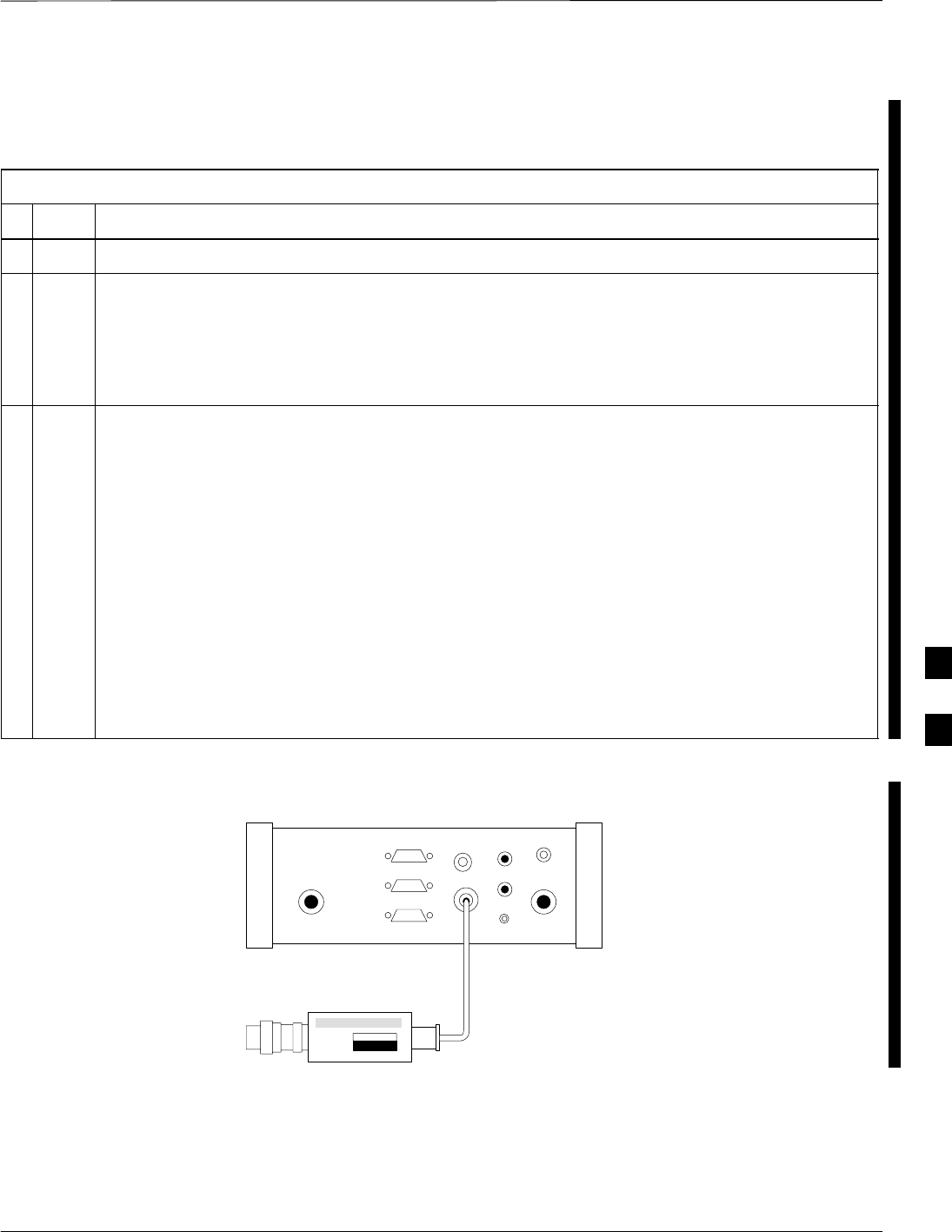
Test Equipment Preparation – continued
FEB 2005 1X SC 4812T Lite BTS Optimization/ATP F-3
PRELIMINARY
Power Sensor Calibration
Table F-3 describes the E7495A Power Sensor Calibration.
Table F-3: E7495A Power Sensor Calibration Procedure
nStep Action
1Display the Power Meter Screen.
2Zero the Power Meter by performing the following actions.
– Make sure you are connected as shown in Figure F-1.
2a Press the Zero Softkey.
2b Press the Continue Softkey.
3Calibrate the Power Meter by performing the following actions.
3a Press Ref CF.
3b Enter the Reference Cal Factor, reading it off the label on the Power Sensor Head.
3c Press Calibrate.
3d Connect the Power Sensor.
– Refer to Figure F-2.
3e Press Continue.
3f Press Cal Factor.
3g Enter the Cal Factor from the label on the Power Sensor Head.
– Select a Cal Factor that is within the operating frequency of the Base Station.
Use only
Agilent supplied
power adapter
GPS
GPIO
Serial 1
Serial 2
Power REF
50 MHz
Sensor
Ext Ref
In
Even Second
Sync In
Antenna
Port 1
RF Out / SWR
Port 2
RF In
POWER SENSOR
NOT CONNECTED
Figure F-1: Agilent E7495A Pre–Power Sensor Calibration Connection
F
Test Equipment Preparation – continued
F-4 1X SC 4812T Lite BTS Optimization/ATP FEB 2005
PRELIMINARY
Use only
Agilent supplied
power adapter
GPS
GPIO
Serial 1
Serial 2
Power REF
50 MHz
Sensor
Ext Ref
In
Even Second
Sync In
Antenna
Port 1
RF Out / SWR
Port 2
RF In
POWER SENSOR
CONNECTED
Figure F-2: Agilent E7495A Power Sensor Calibration Connection
Cable Calibration
Follow the directions in the WinLMF Program to calibrate cables.
– Calibrate the Short Test Cable (refer to Figure 3-15 on Page 3-66)
and two 10 dB Pads to get a Base Line and then calibrate the TX
and RX set–up. Since you need at least 40 dB of Loss when doing
the FER Test, the set–up for RX is the same as TX.
ATP Set–up
TX Path Calibration Set–up is shown in Test Equipment Set–up. Refer
to Figure 3-18 on Page 3-69.
F
Verifying and Setting GPIB Addresses
FEB 2005 1X SC 4812T Lite BTS Optimization/ATP F-5
PRELIMINARY
Agilent E4406A Transmitter
Tester GPIB Address
Refer to Figure F-3 and perform the procedure in Table F-4 to verify
and, if necessary, change the Agilent E4406A GPIB Address.
System Key
Bk Sp
Key
Enter
Key
Data Entry Keypad
Softkey Buttons
Softkey Label Display AreaActive Function Area
ti-CDMA-WP-00085-v01-ildoc-ftw
Figure F-3: Setting Agilent E4406A GPIB Address
Table F-4: Verify and Change Agilent E4406A GPIB Address Procedure
nStep Action
1In the SYSTEM section of the Instrument Front Panel, press the System Key.
– The Softkey Labels displayed on the right side of the instrument screen changes.
2Press the Config I/O Softkey Button to the right of the instrument screen.
– The Softkey Labels changes.
– The current instrument GPIB Address will be displayed below the GPIB Address Softkey Label.
3If the current GPIB Address is not set to 18, perform the following actions to change it.
3a Press the GPIB Address Softkey Button.
– In the on–screen Active Function Area, GPIB Address will be displayed followed by the
current GPIB Address.
table continued on next page
F

Verifying and Setting GPIB Addresses – continued
F-6 1X SC 4812T Lite BTS Optimization/ATP FEB 2005
PRELIMINARY
Table F-4: Verify and Change Agilent E4406A GPIB Address Procedure
nActionStep
3b On the Front Panel Data Entry Keypad, enter the Analyzer GPIB Address of 18.
– The GPIB Address Label changes to Enter.
– Characters typed wi the Keypad replaces the current GPIB Address in the Active Function Area.
NOTE
To correct an entry, press the Bk Sp Key to delete one character at a time.
3c Press the Enter Softkey Button or the Keypad Enter Key to set the new GPIB Address.
– The Config I/O Softkey Labels will re–appear.
– The new GPIB Address will be displayed under the GPIB Address Softkey Label.
F
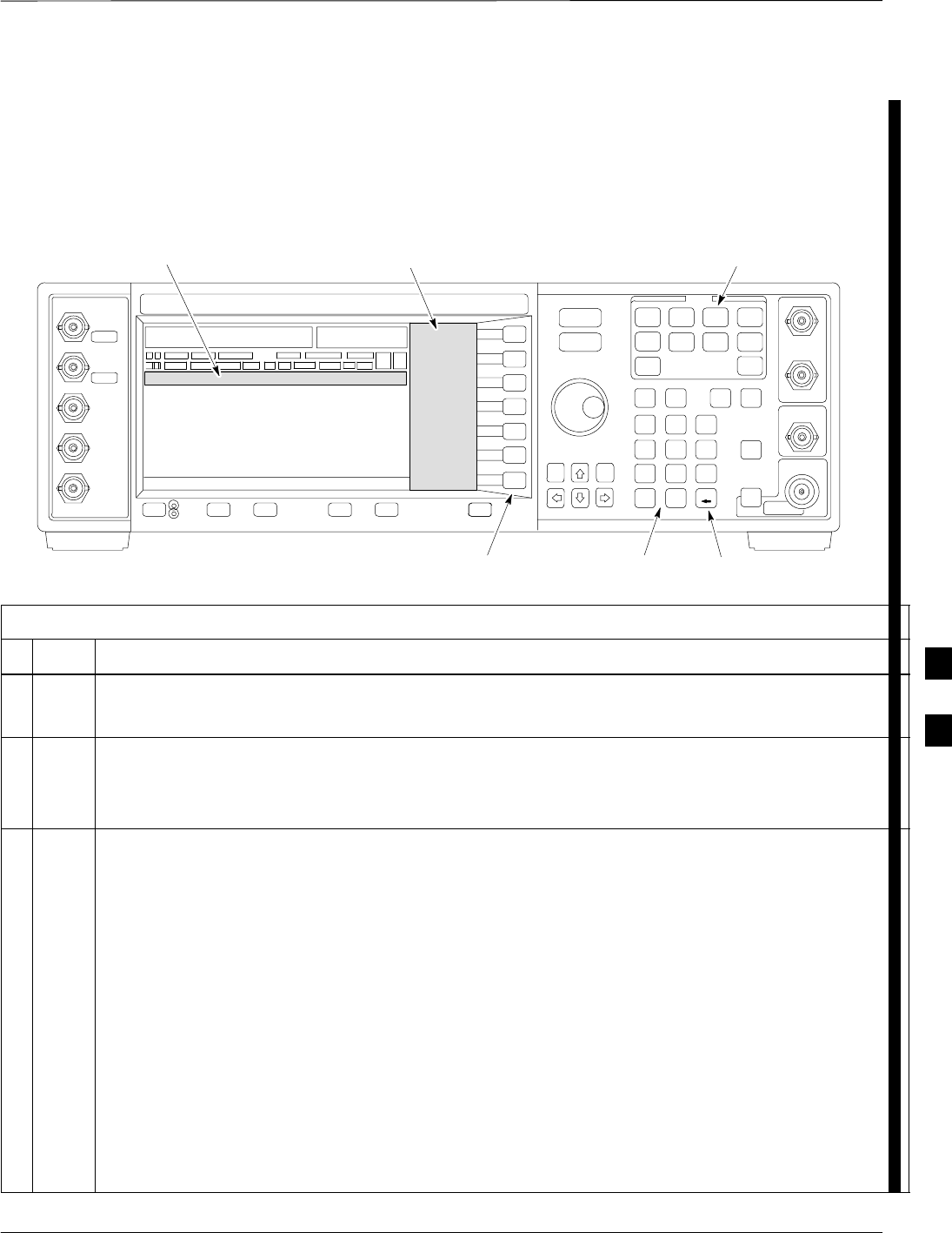
Verifying and Setting GPIB Addresses – continued
FEB 2005 1X SC 4812T Lite BTS Optimization/ATP F-7
PRELIMINARY
Agilent E4432B Signal
Generator GPIB Address
Refer to Figure F-4 and perform the procedure in Table F-5 to verify
and, if necessary, change the Agilent E4432B GPIB Address.
Numeric Keypad
Softkey Buttons
Softkey Label Display AreaActive Entry Area
Backspace Key
Utility Key
Figure F-4: Setting Agilent E4432B GPIB Address
Table F-5: Verify that and Change Agilent E4432B GPIB Address
nStep Action
1In the MENUS section of the Instrument Front Panel, press the Utility Key.
– The Softkey Labels displayed on the right side of the instrument screen changes.
2Press the GPIB/RS232 Softkey Button to the right of the instrument screen.
– The Softkey Labels changes.
– The current instrument GPIB Address will be displayed below the GPIB Address Softkey Label.
3If the current GPIB Address is not set to 1, perform the following to change it:
3a Press the GPIB Address Softkey Button.
– The GPIB Address Label and current GPIB Address changes to boldface.
– In the on–screen Active Entry Area, Address: is displayed followed by the current GPIB Address.
3b On the Front Panel Numeric Keypad, enter the Signal Generator GPIB Address of 1.
– The GPIB Address Label changes to Enter.
– Characters typed in the Keypad replace the current GPIB Address in the Active Entry Display.
NOTE
To correct an entry, press the Backspace Key at the lower right of the Keypad to delete one character at
a time.
3c Press the Enter Softkey Button to set the new GPIB Address.
– The new GPIB Address will be displayed under the GPIB Address Softkey Label.
F
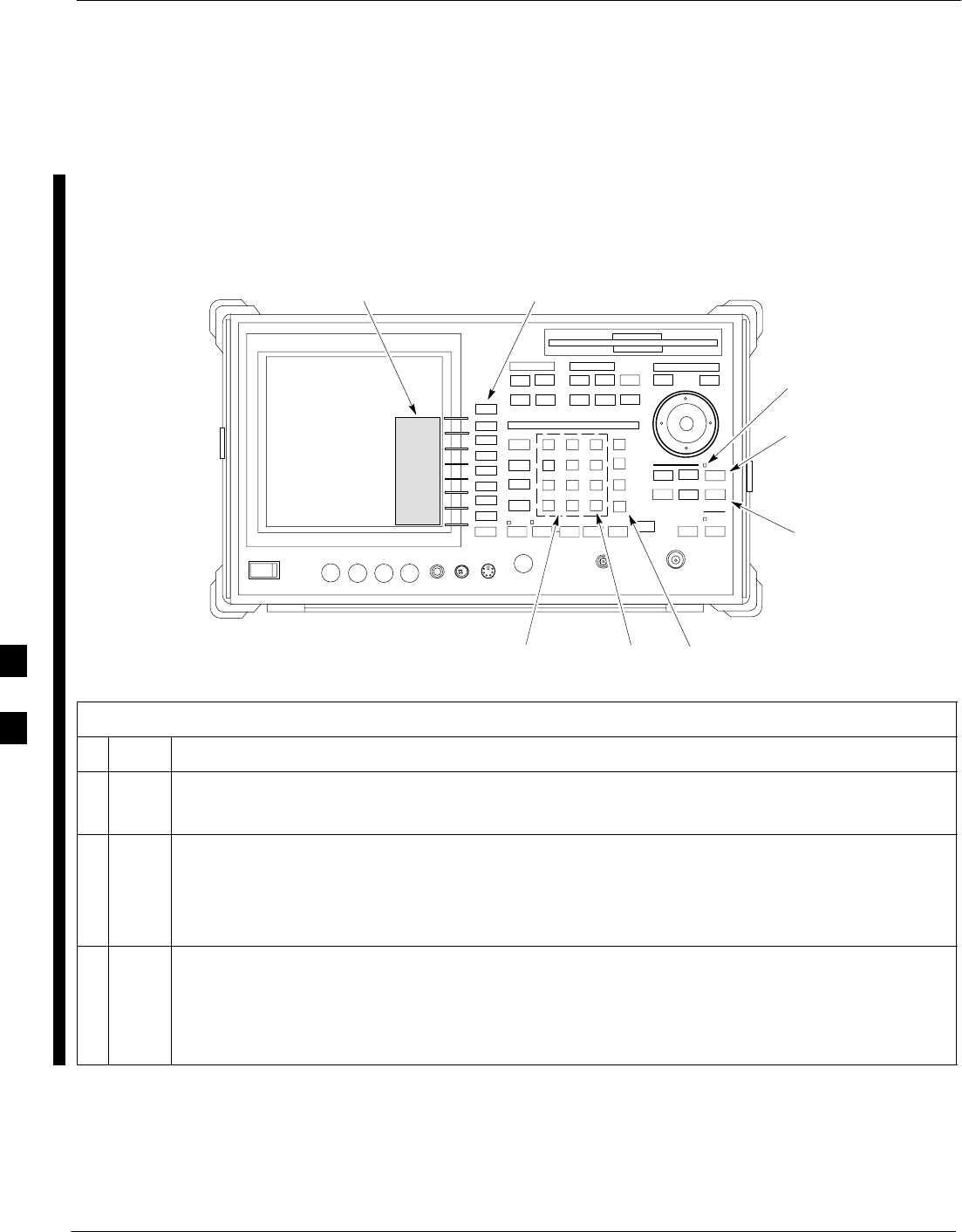
Verifying and Setting GPIB Addresses – continued
F-8 1X SC 4812T Lite BTS Optimization/ATP FEB 2005
PRELIMINARY
Advantest R3267 Spectrum
Analyzer GPIB Address
Refer to Figure F-5 and perform the procedure in Table F-6 to verify
and, if necessary, change the Advantest R3267 Spectrum Analyzer GPIB
Address.
onREMOTE LED
LCL Key
CONFIG Key
Softkey Label Display Area Softkey Buttons
Keypad BS Key ENTR Key
Figure F-5: Setting Advantest R3267 GPIB Address
Table F-6: Verify that and Change Advantest R3267 GPIB Address
nStep Action
1If the REMOTE LED is lighted, press the LCL Key.
– The LED extinguishes.
2Press the CONFIG Key.
–CONFIG Softkey Labels will appear in the Softkey Label display area of the instrument
display.
– The current GPIB Address will be displayed below the GPIB Address Softkey Label.
3If the current GPIB Address is not set to 18, perform the following to change it:
3a Press the GPIB Address Softkey.
–A GPIB Address Entry window will open in the instrument display showing the current
GPIB Address.
table continued on next page
F
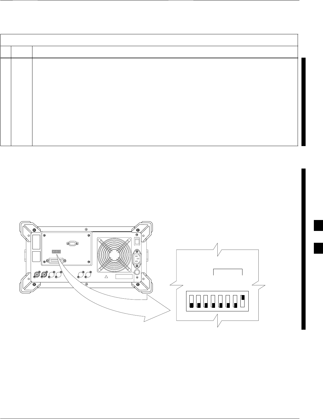
Verifying and Setting GPIB Addresses – continued
FEB 2005 1X SC 4812T Lite BTS Optimization/ATP F-9
PRELIMINARY
Table F-6: Verify that and Change Advantest R3267 GPIB Address
nActionStep
3b Enter 18 on the Keypad in the ENTRY Section of the Instrument Front Panel.
– Characters typed on the Keypad will replace the address displayed in the GPIB Address
Entry Window.
NOTE
To correct an entry, press the BS (Backspace) Key at the lower right of the Keypad to delete one
character at a time.
3c Press the ENTR Key to the lower right of the Keypad to set the new GPIB Address.
– The GPIB Address Entry window closes.
– The new address is displayed in the bottom portion of the GPIB Address Softkey Label.
Advantest R3562 Signal
Generator GPIB Address
Set the GP–IP ADDRESS Switch on the rear of the Advantest R3562
Signal Generator to Address 1 as shown in Figure F-6.
123 45678
54321
GP–IP ADDRESS
1
0
GPIB Address set to “1”
Figure F-6: Advantest R3562 GPIB Address Switch Setting
F
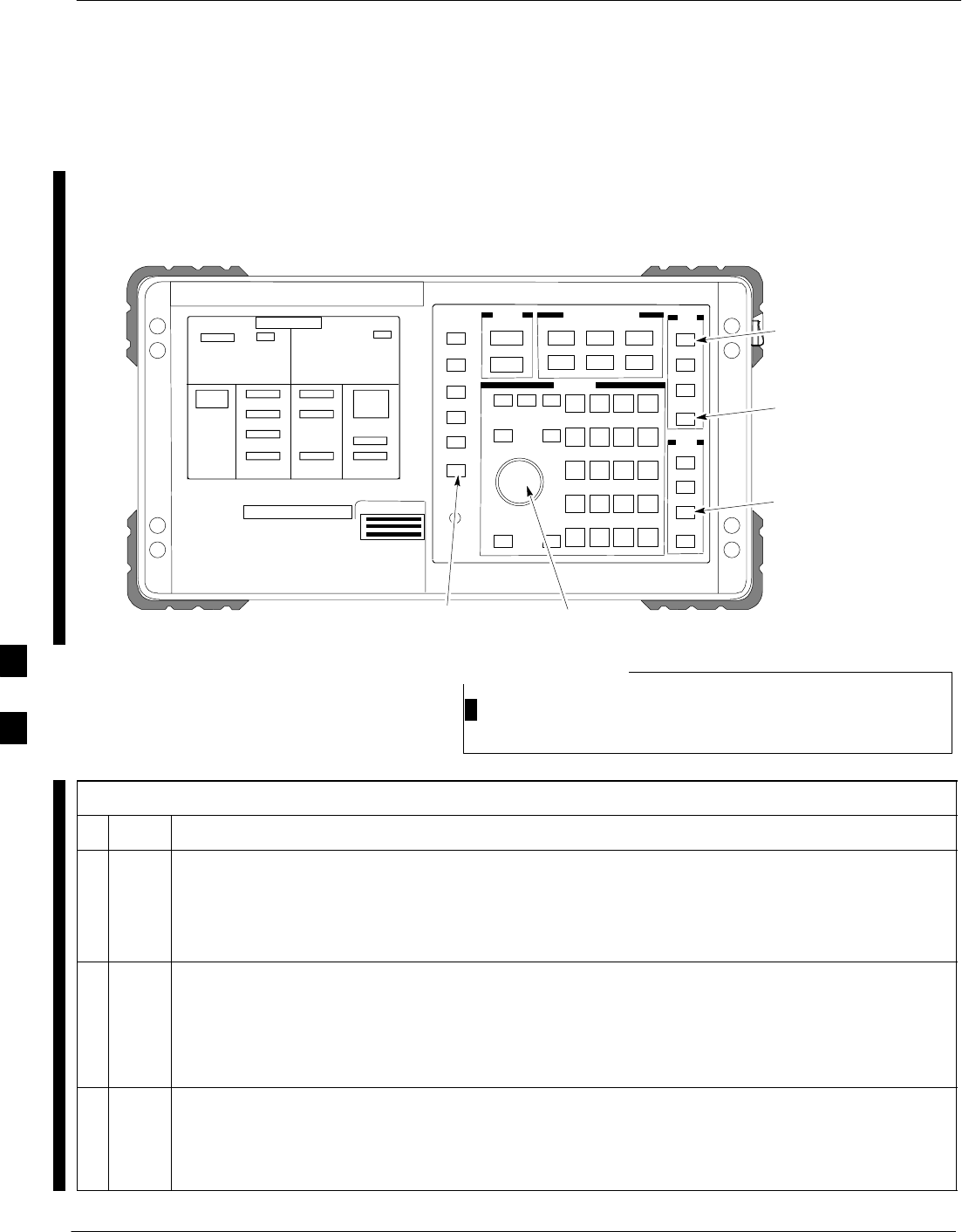
Verifying and Setting GPIB Addresses – continued
F-10 1X SC 4812T Lite BTS Optimization/ATP FEB 2005
PRELIMINARY
Agilent 8935 Series E6380
(formerly HP 8935) Test Set
GPIB Address
Refer to Figure F-7 and perform the procedure in Table F-7 to verify
and, if necessary, change the Agilent 8935 GPIB Address.
Preset
Cursor Control
Shift
Inst Config
Local
FW00885
Figure F-7: Agilent 8935 Test Set
This procedure assumes that the Test Equipment is set–up
and ready for testing.
NOTE
Table F-7: Verify and/or Change Agilent 8935 (formerly HP 8935) GPIB Address Procedure
nStep Action
NOTE
The HP I/O Configuration MUST be set to Talk & Listen, or no device on the GPIB will be
accessible.
– Consult Test Equipment OEM Documentation for additional information as required.
1To verify that the GPIB Addresses are set correctly, press Shift and LOCAL on the Agilent 8935.
– The current HP–IB Address is displayed at the top of the screen.
NOTE
HP–IB is the same as GPIB.
2If the current GPIB Address is not set to 18, perform the following actions to change it:
2a Press Shift and Inst Config.
2b Turn the Cursor Control Knob to move the cursor to the HP–IB Adrs Field.
table continued on next page
F

Verifying and Setting GPIB Addresses – continued
FEB 2005 1X SC 4812T Lite BTS Optimization/ATP F-11
PRELIMINARY
Table F-7: Verify and/or Change Agilent 8935 (formerly HP 8935) GPIB Address Procedure
nActionStep
2c Press the Cursor Control Knob to select the field.
2d Turn the Cursor Control Knob as required to change the address to 18.
2e Press the Cursor Control Knob to set the address.
3 Press Preset to return to normal operation.
F
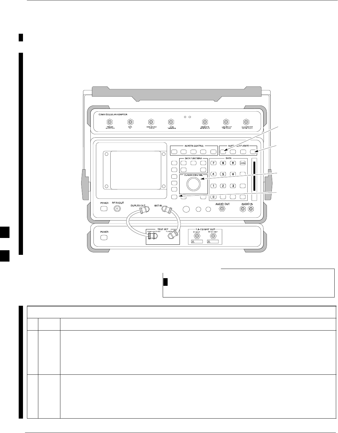
Verifying and Setting GPIB Addresses – continued
F-12 1X SC 4812T Lite BTS Optimization/ATP FEB 2005
PRELIMINARY
Hewlett Packard HP 8921A and
HP83236A/B GPIB Address
Refer to Figure F-8 and perform the procedure in Table F-8 to verify
and, if necessary, change the HP 8921A HP 83236A GPIB Addresses.
Preset
Cursor Control
Shift
Local
Figure F-8: HP 8921A and HP 83236A/B
This procedure assumes that the Test Equipment is set–up
and ready for testing.
NOTE
Table F-8: Verify and/or Change HP 8921A and HP 83236A GPIB Addresses Procedure
nStep Action
1To verify that the GPIB Addresses are set correctly, press Shift and LOCAL on the HP 8921A.
– The current HP–IB Address is displayed at the top of the screen.
NOTE
HP–IB is the same as GPIB.
2If the current HP–IB Address is not set to 18, perform the following actions to change it.
2a Turn the Cursor Control Knob to move the cursor to More and press the knob to select the field.
2b Turn the Cursor Control Knob to move the cursor to I/O Config and press the knob to select the
field.
table continued on next page
F

Verifying and Setting GPIB Addresses – continued
FEB 2005 1X SC 4812T Lite BTS Optimization/ATP F-13
PRELIMINARY
Table F-8: Verify and/or Change HP 8921A and HP 83236A GPIB Addresses Procedure
nActionStep
2c Turn the Cursor Control Knob to move the cursor to Adrs and press the knob to select the field.
2d Turn the Cursor Control Knob to change the HP–IB Address to 18 and press the knob to set the
address.
2e Press Shift and Preset to return to normal operation.
3To set the HP 83236A (or B) PCS Interface GPIB Address = 19, set the DIP Switches as follows:
– A1=1, A2=1, A3=0, A4=0, A5=1, HP–IB/Ser = 1
F
Verifying and Setting GPIB Addresses – continued
F-14 1X SC 4812T Lite BTS Optimization/ATP FEB 2005
PRELIMINARY
Advantest R3465
Communications Test Set GPIB
Address
Refer to Figure F-9 and perform the procedure in Table F-9 to verify
and, if necessary, change the GPIB Address for the Advantest R3465.
BNC
“T”
REF UNLOCK EVEN
SEC/SYNC IN CDMA
TIME BASE IN
POWER
OFF ON
REF FW00337
LCL Shift Preset
GPIB and others
Vernier
Knob
Figure F-9: R3465 Communications Test Set
This procedure assumes that the Test Equipment is set–up
and ready for testing.
NOTE
Table F-9: Verify and/or Change Advantest R3465 GPIB Address Procedure
nStep Action
1To verify that the GPIB Address is set correctly, perform the following:
1a Press SHIFT then PRESET.
1b Press LCL.
1c Press the GPIB and Others CRT Menu Key to view the current address.
2If the current GPIB Address is not set to 18, perform the following actions to change it.
2a Turn the Vernier Knob as required to select 18.
2b Press the Vernier Knob to set the address.
3To return to normal operation, press Shift and Preset.
F

Verifying and Setting GPIB Addresses – continued
FEB 2005 1X SC 4812T Lite BTS Optimization/ATP F-15
PRELIMINARY
Motorola CyberTest GPIB
Address
Perform the procedure in Table F-10 to verify and, if necessary, change
the GPIB Address on the Motorola CyberTest. Changing the GPIB
Address requires the following items:
SMotorola CyberTest Communications Analyzer.
SComputer running Windows 3.1/Windows 95 (or later).
SMotorola CyberTAME Software Program named “TAME”.
SParallel Printer Port Cable (shipped with the CyberTest unit).
This procedure assumes that the Test Equipment is set–up
and ready for testing.
NOTE
Table F-10: Verify and/or Change Motorola CyberTest GPIB Address Procedure
nStep Action
1On the LMF Desktop, locate the CyberTAME Icon.
2Double–click on the CyberTAME Icon to run the CyberTAME Application.
3In the CyberTAME Window Taskbar, under Special, select IEEE.488.2.
– The CyberTAME Software will query the CyberTest Analyzer for its current GPIB Address.
– It then will open the IEEE 488.2 Dialog Box.
4If the current GPIB Address is not 18, perform the following actions to change it.
4a Set the GPIB Address to 18.
– Use the UP and DOWN Increment Arrows.
or
– Double–click in the field and type the number.
4b Click on the OK Button.
– The new address will be written to the CyberTest through the Parallel Port and saved.
5Verify that the address has been set by repeating Steps 3 and 4.
– The new address should now appear in the IEEE 488.2 Dialog Box Address Field.
F
Verifying and Setting GPIB Addresses – continued
F-16 1X SC 4812T Lite BTS Optimization/ATP FEB 2005
PRELIMINARY
HP 437 Power Meter GPIB
Address
Refer to Figure F-10 and follow the steps in Table F-11 to verify and, if
necessary, change the HP 437 GPIB Address.
Enter
Preset
SHIFT (BLUE) PUSHBUTTON –
ACCESSES FUNCTION AND
DATA ENTRY KEYS IDENTIFIED
WITH LIGHT BLUE TEXT ON
THE FRONT PANEL ABOVE
THE BUTTONS
FW00308REF
Figure F-10: HP 437 Power Meter
This procedure assumes that the Test Equipment is set–up
and ready for testing.
NOTE
Table F-11: Verify and/or Change the HP 437 Power Meter GPIB Address Procedure
nStep Action
1 Press Shift and PRESET.
2 Use the y (UP) Arrow Key to navigate to the HP–IB ADRS and press ENTER.
– The HP–IB Address is displayed.
NOTE
HP–IB is the same as GPIB.
3 If the current GPIB Address is not set to 13, perform the following actions to change it.
3a Use the y (UP) and b (DOWN) Arrow Keys to change the HP–IB ADRS to 13.
3b Press ENTER to set the new address.
4 Press Shift and ENTER to return to a standard configuration.
F
Verifying and Setting GPIB Addresses – continued
FEB 2005 1X SC 4812T Lite BTS Optimization/ATP F-17
PRELIMINARY
Gigatronics 8541C Power
Meter GPIB Address
Refer to Figure F-11 and follow the steps in Table F-12 to verify and, if
necessary, change the Gigatronics 8541C Power Meter GPIB Address.
MENU ENTER ARROW
KEYS
1
REF FW00564
Figure F-11: Gigatronics 8541C Power Meter Detail
This procedure assumes that the Test Equipment is set–up
and ready for testing.
NOTE
Table F-12: Verify and/or Change Gigatronics 8541C Power Meter GPIB Address
nStep Action
1! CAUTION
Do not connect/disconnect the Power Meter Sensor Cable with AC Power applied to the meter.
Disconnection could result in destruction of the Sensing Element or miscalibration.
Press MENU.
2Use the b Arrow Key to select CONFIG MENU and press ENTER.
3Use the b Arrow Key to select GPIB and press ENTER.
The current Mode and GPIB Address are displayed.
4If the Mode is not set to 8541C, perform the following to change it:
Use the a ’ Arrow Keys as required to select MODE.
Use the by Arrow Keys as required to set MODE to 8541C.
5If the GPIB Address is not set to 13, perform the following to change it:
Use the ’ Arrow Key to select ADDRESS.
Use the by Arrow Keys as required to set the GPIB Address to 13.
6 Press ENTER to return to normal operation.
F
Verifying and Setting GPIB Addresses – continued
F-18 1X SC 4812T Lite BTS Optimization/ATP FEB 2005
PRELIMINARY
RS232 GPIB Interface Adapter
Ensure that the RS–232 GPIB Interface adapter DIP Switches are set as
shown in Figure F-12.
RS232–GPIB
INTERFACE BOX
S MODE
DATA FORMAT
BAUD RATE
GPIB ADRS
ON
DIP SWITCH SETTINGS
G MODE
Figure F-12: RS232 GPIB Interface Adapter
F

Test Equipment Inter–Unit Connection, Testing, and Control
FEB 2005 1X SC 4812T Lite BTS Optimization/ATP F-19
PRELIMINARY
Inter–Unit Connection, Testing,
and Control Settings
The following illustrations, tables, and procedures provide the
information necessary to prepare various items of CDMA Test
Equipment supported by the LMF for BTS Calibration and/or
Acceptance Testing.
HP 8921A with PCS Interface
Test Equipment Connections
The following diagram depicts the rear panels of the HP 8921A Test
Equipment as configured to perform automatic tests. All Test Equipment
is controlled by the LMF via an IEEE–488/GPIB Bus.
The LMF expects each piece of Test Equipment to have a factory-set
GPIB Address (refer to Table F-8 and Figure F-8). If there is a
communications problem between the LMF and any piece of Test
Equipment, verify that the GPIB Addresses have been set correctly and
that the GPIB Cables are firmly connected to the Test Equipment.
Figure F-13 shows the connections when not using an external 10 MHz
Rubidium Reference.
Table F-13: HP 8921A/600 Communications Test Set Rear Panel Connections
without Rubidium Reference
From Test Set: To Interface:
Connector Type
8921A 83203B CDMA 83236A PCS
C
onnector
T
ype
CW RF OUT CW RF IN SMC–Female – SMC–Female
114.3 MHZ IF OUT 114.3 MHZ IF IN SMC–Female – SMC–Female
IQ RF IN IQ RF OUT SMC–Female – SMC–Female
DET OUT AUX DSP IN SMC–Female – SMC–Female
CONTROL I/O CONTROL I/O 45–pin Custom BUS
10 MHZ OUT SYNTH REF IN BNC–Male – BNC–Male
HPIB INTERFACE HPIB INTERFACE HPIB Cable
10 MHZ OUT REF IN BNC–Male – BNC–Male
F
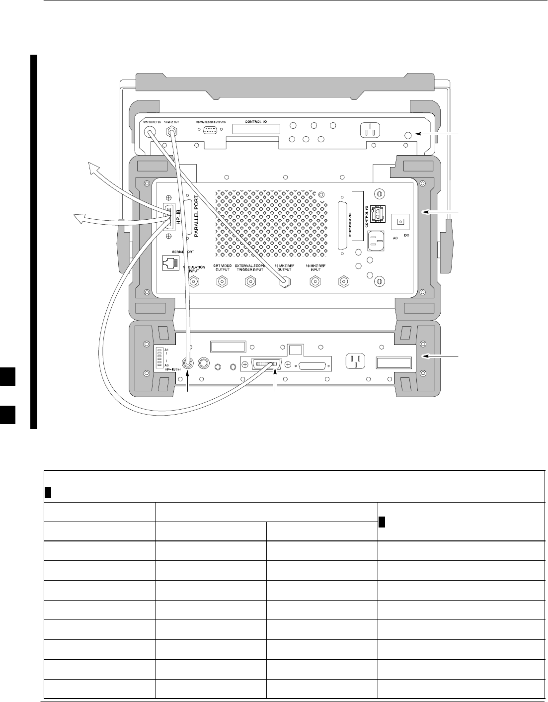
Test Equipment Inter–Unit Connection, Testing, and Control – continued
F-20 1X SC 4812T Lite BTS Optimization/ATP FEB 2005
PRELIMINARY
REAR PANEL
COMMUNICATIONS TEST SET
REF IN
HP 83203B CDMA
CELLULAR ADAPTER
HP 8921A CELL
SITE TEST SET
HP 83236A PCS
INTERFACE
HP–IB
TO GPIB
INTERFACE
BOX
TO POWER
METER GPIB
CONNECTOR
FW00368
Figure F-13: HP 8921A/600 Cable Connections for 10 MHz Signal and GPIB without Rubidium Reference
Table F-14: HP 8921A/600 Communications Test Set Rear Panel Connections
with Rubidium Reference
From Test Set: To Interface:
Connector Type
8921A 83203B CDMA 83236A PCS
C
onnector
T
ype
CW RF OUT CW RF IN SMC–Female – SMC–Female
114.3 MHZ IF OUT 114.3 MHZ IF IN SMC–Female – SMC–Female
IQ RF IN IQ RF OUT SMC–Female – SMC–Female
DET OUT AUX DSP IN SMC–Female – SMC–Female
CONTROL I/O CONTROL I/O 45–pin custom BUS
10 MHZ OUT REF IN BNC–Male – BNC–Male
HPIB INTERFACE HPIB INTERFACE HPIB Cable
10 MHZ INPUT 10 MHZ OUT BNC–Male – BNC–Male
F
Test Equipment Inter–Unit Connection, Testing, and Control – continued
FEB 2005 1X SC 4812T Lite BTS Optimization/ATP F-21
PRELIMINARY
Figure F-14 shows the connections when using an external 10 MHz
Rubidium Reference.
REF IN
REAR PANEL
COMMUNICATIONS TEST SET
TO POWER
METER GPIB
CONNECTOR
TO GPIB
INTERFACE
BOX
10 MHZ WITH
RUBIDIUM STANDARD
HP 83203B CDMA
CELLULAR ADAPTER
HP 8921A CELL
SITE TEST SET
HP 83236A PCS
INTERFACE
HP–IB
FW00369
Figure F-14: HP 8921A/600 Cable Connections for 10 MHz Signal and GPIB with Rubidium Reference
F

Test Equipment Inter–Unit Connection, Testing, and Control – continued
F-22 1X SC 4812T Lite BTS Optimization/ATP FEB 2005
PRELIMINARY
HP 8921A with PCS Interface
System Connectivity Test
Perform the procedure in Table F-15 to verify that the connections
between the PCS Interface and the HP 8921A are correct and cables are
intact. The software also performs basic functionality checks of each
instrument.
Disconnect other GPIB Devices, especially system
controllers, from the system before running the
connectivity software.
NOTE
Table F-15: System Connectivity Test Procedure
nStep Action
NOTE
Perform this procedure only after Test Equipment has been allowed to warm–up and stabilize for a
minimum of 60 minutes.
1Insert the HP 83236A Manual Control/System Card into the Memory Card Slot.
2Press the [PRESET] Pushbutton.
3Press the Screen Control [TESTS] Pushbutton to display the “Tests” Main Menu Screen.
4Position the cursor on Select Procedure Location and select it by pressing the Cursor Control
Knob.
5In the Choices Selection Box, select Card.
6Position the cursor on Select Procedure Filename and select it by pressing the Cursor Control
Knob.
7In the Choices Selection Box, select SYS_CONN.
8Position the cursor on RUN TEST and select it.
– The software will provide operator prompts through completion of the Connectivity Set–up.
9Perform the following action when the test is complete.
– Position cursor on STOP TEST and select it.
OR
– Press the [K5] Pushbutton.
10 To return to the Main Menu, press the [K5] Pushbutton.
11 Press the [PRESET] Pushbutton.
F

Test Equipment Inter–Unit Connection, Testing, and Control – continued
FEB 2005 1X SC 4812T Lite BTS Optimization/ATP F-23
PRELIMINARY
Pretest Set–up for HP 8921A
Before the HP 8921A CDMA Analyzer is used for LMF–controlled
testing, it must be set–up correctly for automatic testing.
Table F-16: Pretest Set–up for HP 8921A
nStep Action
1Unplug the Memory Card if it is plugged in.
2Press the CURSOR CONTROL Knob.
3Position the cursor on IO CONFIG (under To Screen and More) and select it.
4Select Mode and set for Talk&Lstn.
Pretest Set–up for Agilent 8935
Before the Agilent 8935 Analyzer is used for LMF–controlled testing, it
must be set–up correctly for automatic testing.
Table F-17: Pretest Set–up for Agilent 8935
nStep Action
1Unplug the Memory Card if it is plugged in.
2Press the Shift Button and then press the I/O Config Button.
3Press the Push to Select Knob.
4Position the cursor on IO CONFIG and select it.
5 Select Mode and set for Talk&Lstn.
F
Test Equipment Inter–Unit Connection, Testing, and Control – continued
F-24 1X SC 4812T Lite BTS Optimization/ATP FEB 2005
PRELIMINARY
Advantest R3465 Connection
The following diagram depicts the Rear Panel of the Advantest R3465
Test Equipment as configured to perform automatic tests. All Test
Equipment is controlled by the LMF via an IEEE–488/GPIB Bus. The
LMF expects each piece of Test Equipment to have a factory-set GPIB
Address. Refer to Table F-9 and Figure F-9.
If there is a communications problem between the LMF and any piece of
Test Equipment, verify that the GPIB Addresses have been set correctly
and that the GPIB Cables are firmly connected to the Test Equipment.
Figure F-15 shows the connections when not using an external 10 MHz
Rubidium Reference.
ADVANTEST R3465
REAR PANEL
GPIB
CONNECTOR
SERIAL I/O
LOCAL IN
SERIAL I/O
SYN REF IN 10 MHZ OUT
PARALLEL
EXT TRIGGER
10 MHZ REF
GATE IN
GPIB
CDMA CLOCK OUT
AC POWER
AC POWER
R3561L
REAR PANEL
R3465
REAR PANEL
TO T–CONNECTOR
ON FRONT PANEL
(EVEN/SEC/SYNC IN)
XYZ
IF OUT
421 MHZ
TO POWER METER
GPIB CONNECTOR
TO GPIB
INTERFACE BOX
FW00370
Figure F-15: Cable Connections for Test Set without 10 MHz Rubidium Reference
F
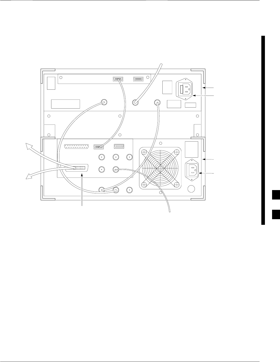
Test Equipment Inter–Unit Connection, Testing, and Control – continued
FEB 2005 1X SC 4812T Lite BTS Optimization/ATP F-25
PRELIMINARY
Figure F-16 shows the connections when using an external 10 MHz
Rubidium Reference.
SERIAL I/O
GPIB
CONNECTOR ADVANTEST R3465
REAR PANEL
FROM 10 MHZ
RUBIDIUM REFERENCE
LOCAL IN
SERIAL I/O
IF OUT
SYN REF IN 10 MHZ OUT
PARALLEL
EXT TRIGGER
10 MHZ REF
GATE IN
GPIB
CDMA CLOCK OUT
AC POWER
AC POWER
R3465/3463
REAR PANEL
R3561L
REAR PANEL
TO T–CONNECTOR
ON FRONT PANEL
(EVEN SEC/SYNC IN)
XYZ
421 MHZ
TO POWER METER
GPIB CONNECTOR
TO GPIB
INTERFACE BOX
FW00371
Figure F-16: Cable Connections for Test Set with 10 MHz Rubidium Reference
F

Test Equipment Inter–Unit Connection, Testing, and Control – continued
F-26 1X SC 4812T Lite BTS Optimization/ATP FEB 2005
PRELIMINARY
R3465 GPIB Clock Set–up
Table F-18 describes the steps to set the clock for the Advantest R3465
Equipment.
Table F-18: Advantest R3465 Clock Set–up Procedure
nStep Action
1Observe the current date and time displayed in upper right of the CRT Display.
2If the date and time are incorrect, perform the following to change them:
2a Push the Date/Time CRT Menu Key.
2b Rotate the Vernier Knob to select and set.
2c Push the Vernier Knob to enter.
2d Press the SHIFT Button, then press the PRESET Button (just below the CRT Display).
Pretest Set–up for Advantest
R3465
Before the Advantest R3465 Analyzer is used for LMF–controlled
testing, it must be set–up correctly for automatic testing.
Table F-19: Pretest Set–up for Advantest R346
nStep Action
1Press the SHIFT Button so the LED next to it is illuminated.
2Press the RESET Button.
F
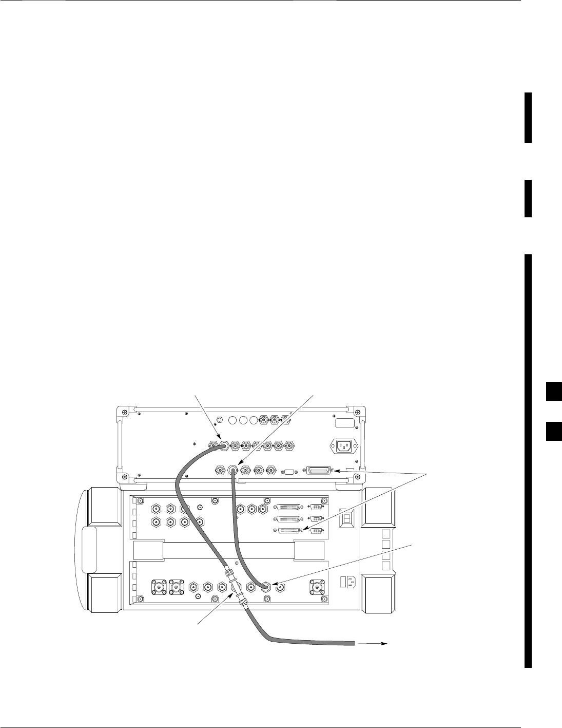
Test Equipment Inter–Unit Connection, Testing, and Control – continued
FEB 2005 1X SC 4812T Lite BTS Optimization/ATP F-27
PRELIMINARY
Agilent 8932/E4432B Test
Equipment Interconnection
To perform FER Testing on a 1X BTS with the Agilent 8935, a
1X–capable Signal Generator, such as the Agilent E4432B, must be used
in conjunction with the CDMA Base Station Test Set. For proper
operation, the Test Equipment Items must be interconnected as follows.
10 MHz Reference Signal
Connect a BNC (M)–BNC (M) Cable from the 8935 10 MHz REF
OUT Connector to the E4432B 10MHz IN Connector as shown in
Figure F-17.
Even Second Pulse Reference
Refer to Figure F-17, and connect a BNC “T” Connector to the 8935
EVEN SEC SYNC IN Connector.
– Connect a BNC (M)–BNC (M) Cable from one side of the BNC
“T” to the E4432B PATTERN TRIG IN Connector.
– Connect the other side of the BNC “T” to the CSM Card SYNC
MONITOR Connector using a BNC (M)–BNC (M) Cable..
E4432B
10 MHz IN
TO GPIB
E4432B
PATTERN TRIG IN
TO CSM BOARD
SYNCH MONITOR
(EVEN SEC TICK)
8935
10 MHz
REF OUT
8935
EVEN SECOND
SYNC IN
WITH BNC “T” TDME0011–1
Figure F-17: Agilent 8935/E4432B 10MHz Reference and Even Second Clock Connections
F
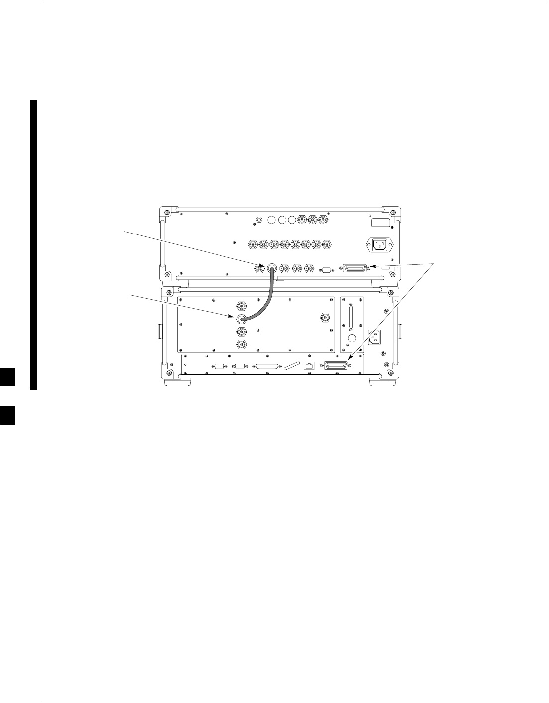
Test Equipment Inter–Unit Connection, Testing, and Control – continued
F-28 1X SC 4812T Lite BTS Optimization/ATP FEB 2005
PRELIMINARY
Agilent E4406A/E4432B Test
Equipment Interconnection
To provide proper operation during testing when both units are required,
the 10 MHz Reference Signal from the E4406A Transmitter Test Set
must be provided to the E4432B Signal Generator.
– Connect a BNC (M)–BNC (M) Cable from the E4406A 10 MHz
OUT (SWITCHED) Connector to the E4432B 10MHz IN
Connector as shown in Figure F-18.
E4406A
10 MHz OUT
(SWITCHED)
E4432B
10 MHz IN
TO GPIB BOX
TDME0009–1
Figure F-18: Agilent 10 MHz Reference Connections
F
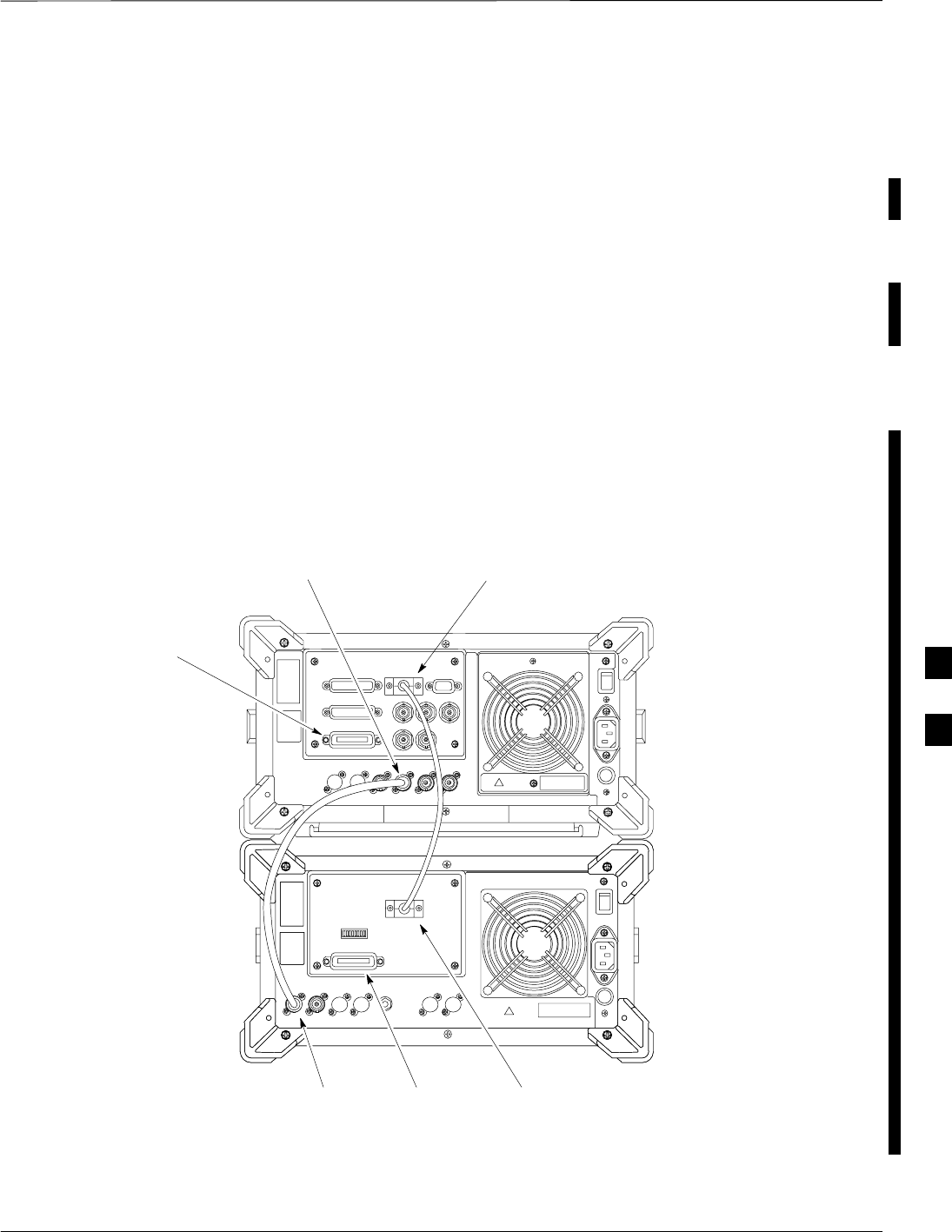
Test Equipment Inter–Unit Connection, Testing, and Control – continued
FEB 2005 1X SC 4812T Lite BTS Optimization/ATP F-29
PRELIMINARY
Advantest R3267/R3562 Test
Equipment Interconnection
To provide proper operation during testing when both units are required,
the R3257 Spectrum Analyzer must be interconnected with the R3562
Signal Generator as follows:
10 MHz Reference Signal
Connect a BNC (M)–BNC (M) Cable between the R3562 SYNTHE
REF IN Connector and the R3267 10 MHz OUT Connector as shown
in Figure F-19..
Serial I/O
Using the AdvanTest Cable provided, connect the R3267 SERIAL I/O
Connector to the R3562 SERIAL I/O Connector as shown in
Figure F-19..
TDME0010–1
R3562
SYNTHE REF IN TO GPIB
BOX R3562
SERIAL I/O
TO GPIB BOX
R3267
10 MHZ OUT R3267
SERIAL I/O
Figure F-19: Advantest 10 MHz Reference and Serial I/O Connections
F
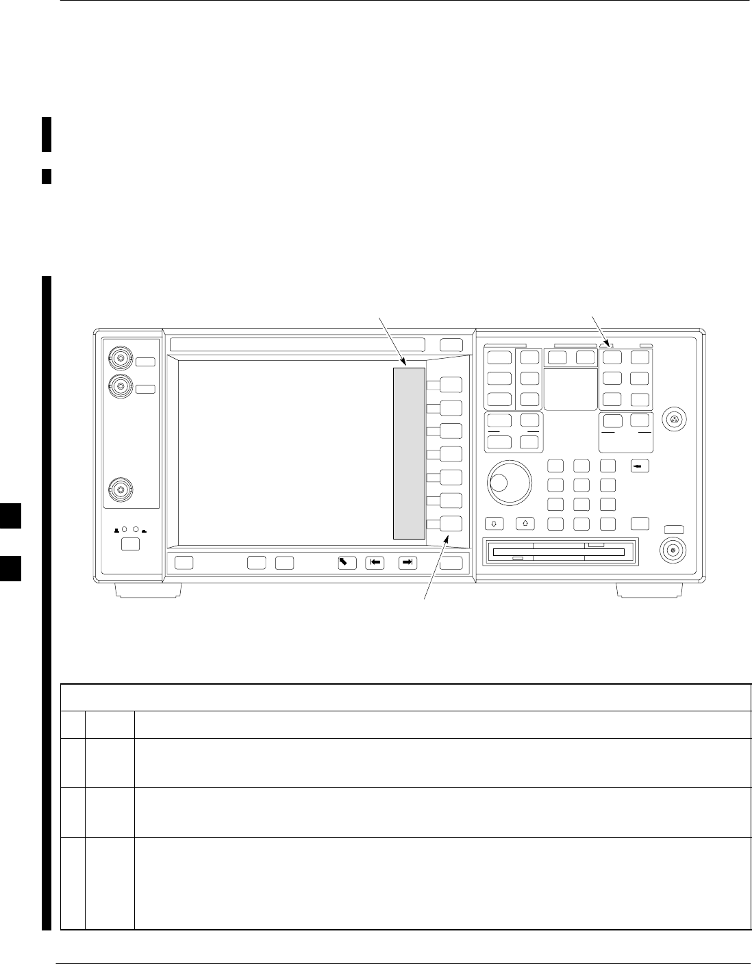
Equipment Calibration
F-30 1X SC 4812T Lite BTS Optimization/ATP FEB 2005
PRELIMINARY
Calibration Without the LMF
Several Test Equipment Items used in the Optimization Process require
Pre–Calibration actions or Calibration Verification that are not supported
by the LMF. Procedures to perform these activities for the applicable
Test Equipment Items are covered in this section.
Agilent E4406A Transmitter
Tester Self–alignment
(Calibration)
System Key
Softkey Buttons
Softkey Label Display Area
Figure F-20: Performing Agilent E4406A Self–alignment (Calibration)
Refer to Figure F-20 and perform the procedure in Table F-20 to perform
the Agilent E4406A Self–alignment (Calibration).
Table F-20: Agilent E4406A Self–alignment (Calibration) Procedure
nStep Action
1In the SYSTEM section of the Instrument Front Panel, press the System Key.
– The Softkey Labels displayed on the right side of the instrument screen changes.
2Press the Alignments Softkey Button to the right of the instrument screen.
– The Softkey Labels changes.
3Press the Align All Now Softkey Button.
– All other instrument functions will be suspended during the alignment.
– The display changes to show progress and results of the alignments performed.
– The alignment will take less than one minute.
F
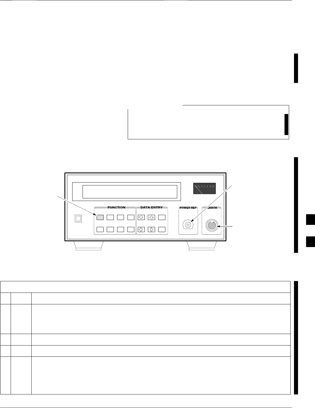
Equipment Calibration – continued
FEB 2005 1X SC 4812T Lite BTS Optimization/ATP F-31
PRELIMINARY
Calibrating HP 437 Power
Meter
Precise Transmit Output Power Calibration Measurements are made
using a Bolometer–type Broadband Power Meter with a sensitive Power
Sensor. Perform the procedure in Table F-21 to enter information unique
to the Power Sensor before calibrating the Test Set–up. Refer to
Figure F-21 as required.
This procedure must be done before the Automated
Calibration to enter Power Sensor–specific Calibration
Values.
NOTE
CONNECT POWER
SENSOR WITH POWER
METER TURNED OFF
CONNECT POWER SENSOR
TO POWER REFERENCE
WHEN CALIBRATING UNIT.
POWER REFERENCE IS
ENABLED USING THE SHIFT ’
KEYS
SHIFT (BLUE) PUSHBUTTON –
ACCESSES FUNCTION AND
DATA ENTRY KEYS IDENTIFIED
WITH LIGHT BLUE TEXT ON
THE FRONT PANEL ABOVE
THE BUTTONS
FW00308
Figure F-21: Power Meter Detail
Table F-21: HP 437 Power Meter Calibration Procedure
nStep Action
! CAUTION
Do not connect/disconnect the Power Meter Sensor Cable with AC Power applied to the meter.
– Disconnection could result in destruction of the Sensing Element or mis–calibration.
1Make sure the Power Meter AC LINE Pushbutton is OFF.
2Connect the Power Sensor Cable to the SENSOR Input.
3Set the AC LINE Pushbutton to ON.
* IMPORTANT
The Calibration should be performed only after the Power Meter and Sensor have been allowed to
warm–up and stabilize for a minimum of 60 minutes.
table continued on next page
F
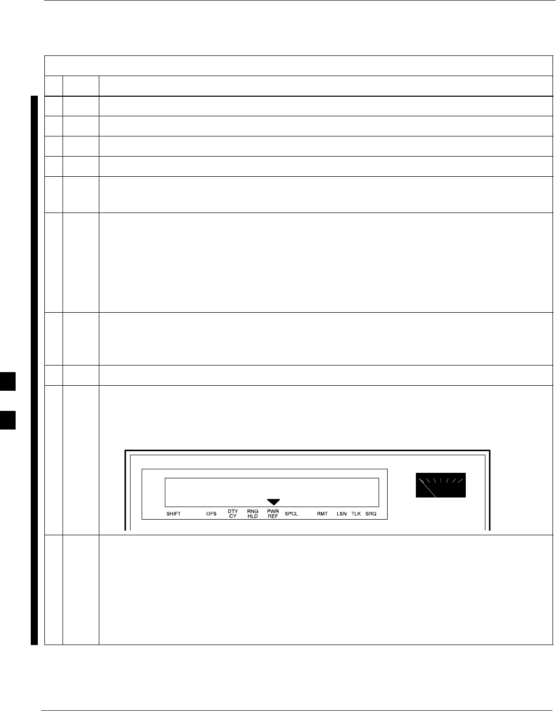
Equipment Calibration – continued
F-32 1X SC 4812T Lite BTS Optimization/ATP FEB 2005
PRELIMINARY
Table F-21: HP 437 Power Meter Calibration Procedure
nActionStep
4Perform the following actions to set or verify that the correct Power Sensor Model:
4a Press [SHIFT] then [a] to select SENSOR.
4b Identify the Power Sensor Model Number from the Sensor Label.
4c Use the [y] or [b] Button to select the appropriate model; then press [ENTER].
5Ensure that the Power Reference Output is OFF.
– Refer to the illustration for Step 9.
6Observe the instrument display to determine if the triangular indicator over PWR REF is
displayed.
SIf the triangular indicator is not displayed, proceed to Step 7.
SIf the triangular indicator is displayed:
–Proceed to Step 8.
– Press [SHIFT] then [’] to turn it off.
7 Press [ZERO].
– The display will show “Zeroing ******.”
– Wait for the process to complete.
8Connect the Power Sensor to the POWER REF Output.
9Turn on the PWR REF by performing the following actions.
9a Press [SHIFT] then [’].
9b Verify that the triangular indicator (below) appears in the display above PWR REF.
10 Perform the following actions to set the REF CF%.
10a Press ([SHIFT] then [ZERO]) for CAL.
10b Enter the Sensor’s REF CF% from the Sensor’s Decal using the Arrow Keys and press [ENTER].
– The Power Meter will display ”CAL *****” for a few seconds.
NOTE
If the REF CAL FACTOR (REF CF) is not shown on the Power Sensor, assume it to be 100%.
table continued on next page
F

Equipment Calibration – continued
FEB 2005 1X SC 4812T Lite BTS Optimization/ATP F-33
PRELIMINARY
Table F-21: HP 437 Power Meter Calibration Procedure
nActionStep
11 Perform the following actions to set the CAL FAC %:
11a Press [SHIFT] then [FREQ] for CAL FAC.
11b On the Sensor’s Decal, locate an approximate Calibration Percentage Factor (CF%) at 2 GHz.
11c Enter the Sensor’s Calibration % (CF%) using the Arrow Keys and press [ENTER].
– When complete, the Power Meter will typically display 0.05 dBm; any reading between 0.00
and 0.10 is normal.
12 To turn off the PWR REF, perform the following actions.
12a Press [SHIFT] then [’].
12b Disconnect the Power Sensor from the POWER REF Output.
F
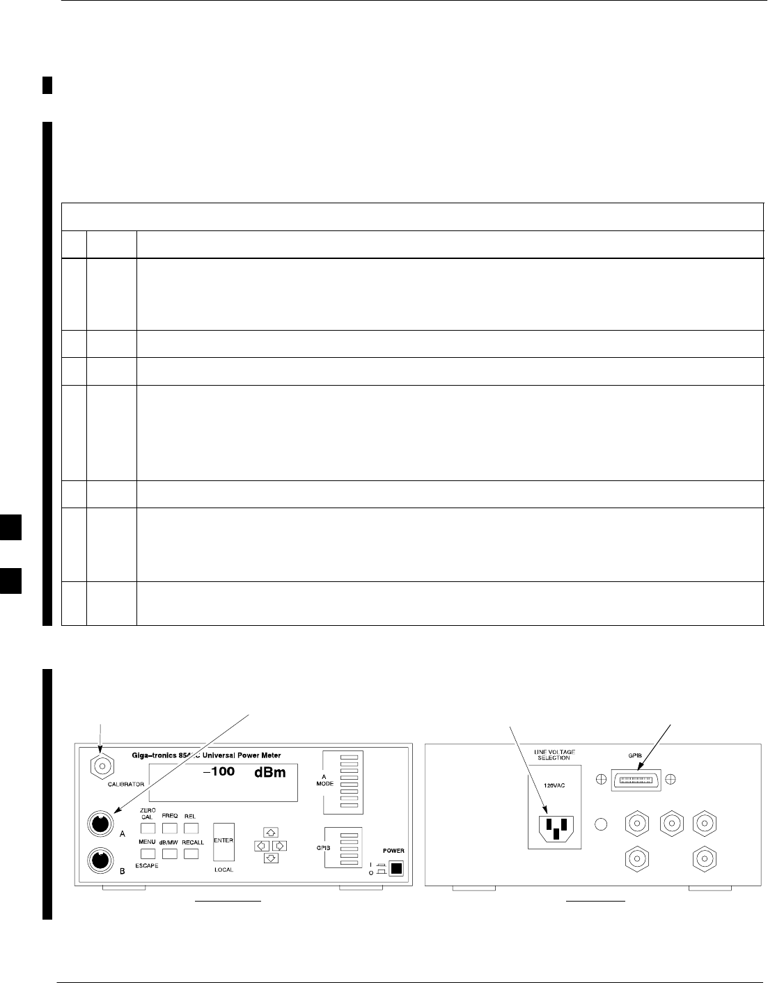
Equipment Calibration – continued
F-34 1X SC 4812T Lite BTS Optimization/ATP FEB 2005
PRELIMINARY
Calibrating the Gigatronics
8541C Power Meter
Precise transmit Output Power Calibration measurements are made using
a Bolometer–type Broadband Power Meter with a sensitive Power
Sensor. Perform the procedure in Table F-22 to enter information unique
to the Power Sensor.
Table F-22: Gigatronics 8541C Power Meter Calibration Procedure
nStep Action
! CAUTION
Do not connect/disconnect the Power Meter Sensor Cable while AC Power is applied to the meter.
– Disconnection could result in destruction of the Sensing Element or miscalibration.
1Make sure the Power Meter POWER Pushbutton is OFF.
3Connect the Power Sensor Cable to the SENSOR Input.
4Set the POWER Pushbutton to ON.
NOTE
Allow the Power Meter and sensor to warm–up and stabilize for a minimum of 60 minutes before
performing the Calibration Procedure.
5Connect the Power Sensor to the CALIBRATOR Output Connector.
6 Press ZERO.
– Wait for the process to complete.
– Sensor Factory Calibration Data is read to Power Meter during this process.
7When the Zeroing Process is complete, disconnect the Power Sensor from the CALIBRATOR
Output.
CONNECT POWER SENSOR
WITH POWER METER
TURNED OFF
CONNECT POWER SENSOR TO
CALIBRATOR POWER REFERENCE
WHEN CALIBRATING/ZEROING UNIT
FRONT View REAR View
GPIB CONNECTIONAC POWER
FW00564
Figure F-22: Gigatronics 8541C Power Meter Detail
F

Manual Cable Calibration
FEB 2005 1X SC 4812T Lite BTS Optimization/ATP F-35
PRELIMINARY
Calibrating the Test Cable
Set–up using HP PCS Interface
(HP83236)
Table F-23 covers the procedure to calibrate the Test Equipment using
the HP8921 Cellular Communications Analyzer equipped with the
HP83236 PCS Interface.
This calibration method must be executed with great care.
Some Losses are measured close to the minimum limit of
the Power Meter Sensor (–30dBm).
NOTE
Prerequisites
Ensure the following prerequisites have been met before proceeding:
STest Equipment to be calibrated has been connected correctly for
Cable Calibration.
STest Equipment has been selected and calibrated.
Table F-23: Test Cable Set–up (using the HP PCS Interface) Calibration Procedure
nStep Action
NOTE
Verify that GPIB Controller is turned off.
1Insert the HP83236 Manual Control System Card into the Memory Card Slot.
2Press the Preset Pushbutton.
3Under Screen Controls, press the TESTS Pushbutton to display the TESTS (Main Menu) Screen.
2Position the cursor on Select Procedure Location and select it.
3In the Choices Selection Box, select CARD.
4Position the cursor on Select Procedure Filename and select it.
5In the Choices Selection Box, select MANUAL.
6Position the cursor on RUN TEST and select it.
– The HP Analyzer must be in Control Mode.
7 Select YES.
8Proceed based upon the analyzer being used.
SIf the HP83236A is being used, proceed to Step 9.
SIf the HP83236B is being used, proceed to Step 10.
table continued on next page
F

Manual Cable Calibration – continued
F-36 1X SC 4812T Lite BTS Optimization/ATP FEB 2005
PRELIMINARY
Table F-23: Test Cable Set–up (using the HP PCS Interface) Calibration Procedure
nActionStep
9Set the Channel Number=<chan#> by performing the following actions.
9a Position the cursor on Channel Number and select it.
9b Enter the chan# using the Numeric Keypad.
9c Press [Enter].
– The screen will go blank.
– When the screen reappears, the chan# will be displayed on the Channel Number Line.
9d Proceed to Step 11.
10 Set the Channel Frequency by performing the following actions.
10a Position the cursor on Frequency Band and press Enter.
10b Select User Defined Frequency.
10c Go Back to Previous Menu.
10d Position the cursor to 83236 Generator Frequency and enter actual RX Frequency.
10e Position the cursor to 83236 Analyzer Frequency and enter actual TX Frequency.
11 Set the RF Generator Level by performing the following actions.
11a Position the cursor on RF Generator Level and select it.
11b Enter –10 using the Numeric Keypad.
11c Press [Enter].
– The screen will go blank.
– When the screen reappears, the value –10 dBm will be displayed on the RF Generator Level
Line.
12 Set the user–fixed Attenuation Setting to 0 dBm by performing the following actions.
12a Position the cursor on Analyzer Attenuation and select it
12b Position the cursor on User Fixed Atten Settings and select it.
12c Enter 0 (zero) using the Numeric Keypad and press [Enter].
13 Select Back to Previous Menu.
14 Record the Generator Frequency Level .
SIf using the HP83226A, proceed to Step 15.
SIf using the HP83226B, proceed to Step 16.
table continued on next page
F

Manual Cable Calibration – continued
FEB 2005 1X SC 4812T Lite BTS Optimization/ATP F-37
PRELIMINARY
Table F-23: Test Cable Set–up (using the HP PCS Interface) Calibration Procedure
nActionStep
15 HP83226A: Perform the following actions.
15a Position the cursor on Show Frequency and Level Details and select it.
15b Under HP83236 Frequencies and Levels, record the Generator Level.
15c Position the cursor on Prev Menu and select it.
15d Proceed to Step 17.
16 HP83226B: Perform the following actions.
16a Position the cursor on Show Frequency and Level Details and select it.
16b Under HP83236B Frequencies and Levels, record the Generator Frequency Level (1850 –
1910 MHz).
16c Position the cursor on Prev Menu and select it.
17 Click on Pause for Manual Measurement.
18 Connect the Power Sensor directly to the RF OUT ONLY Port of the PCS Interface.
19 On the HP 8921A, under To Screen, select CDMA GEN.
20 Move the cursor to the Amplitude field and click on the Amplitude Value.
21 Increase the Amplitude Value until the Power Meter reads 0 dBm ±0.2 dB.
NOTE
The Amplitude Value can be increased coarsely until 0 dBM is reached; then fine tune the
Amplitude by adjusting the Increment Set to 0.1 dBm and targeting in on 0 dBm.
22 Disconnect the Power Sensor from the RF OUT ONLY port of the PCS Interface.
NOTE
The Power Meter Sensor’s lower limit is –30dBm. Thus, only components having losses ≤30 dB
should be measured using this method.
For further accuracy, always re-zero the Power Meter before connecting the Power Sensor to
the component being calibrated.
–After connecting the Power Sensor to the component, record the calibrated Loss
immediately.
23 Disconnect all components in the Test Set–up in order to calibrate each component separately.
23a Connect each component, one-at-a-time, between the RF OUT ONLY PORT and the Power Sensor.
23b Record the calibrated Loss Value displayed on the Power Meter.
SExample: (A) Test Cable(s) = –1.4 dB
(B) 20dB Attenuator = –20.1 dB
(B) Directional Coupler = –29.8 dB
24 After all components have been calibrated, re–assemble all of the components back together.
table continued on next page
F

Manual Cable Calibration – continued
F-38 1X SC 4812T Lite BTS Optimization/ATP FEB 2005
PRELIMINARY
Table F-23: Test Cable Set–up (using the HP PCS Interface) Calibration Procedure
nActionStep
25 Calculate the Total Test Set–up Loss Value by adding up all the individual Loss Values:
SExample: Total Test Set–up Loss Value = –1.4 –29.8 –20.1 = –51.3 dB.
– This calculated value will be used in the next series of tests.
26 Under Screen Controls press the TESTS Button to display the TESTS (Main Menu) Screen.
27 Select Continue (K2).
28 Select RF Generator Level and set to –119 dBm.
29 Click on Pause for Manual Measurement.
30 Verify the GPIB (HP–IB) Address (HP 8921A Communication Analyzer/83203A CDMA
Interface).
– Fields not specifically identified remain at default values.
30a Under To Screen, select More.
30b Select IO CONFIG.
30c Set HP–IB Adrs to 18.
30d Set Mode to Talk&Lstn.
31 Verify that the HP 8921A is displaying Frequency instead of RF Channel.
31a Press the blue [SHIFT] Button, then press the Screen Control [DUPLEX] Button; this switches to
the CONFIG (CONFIGURE) Screen.
31b Use the Cursor Control to set RF Display to Freq.
32 Refer to Chapter 3 for assistance in setting the Test Cable Insertion Loss Values into the LMF.
F
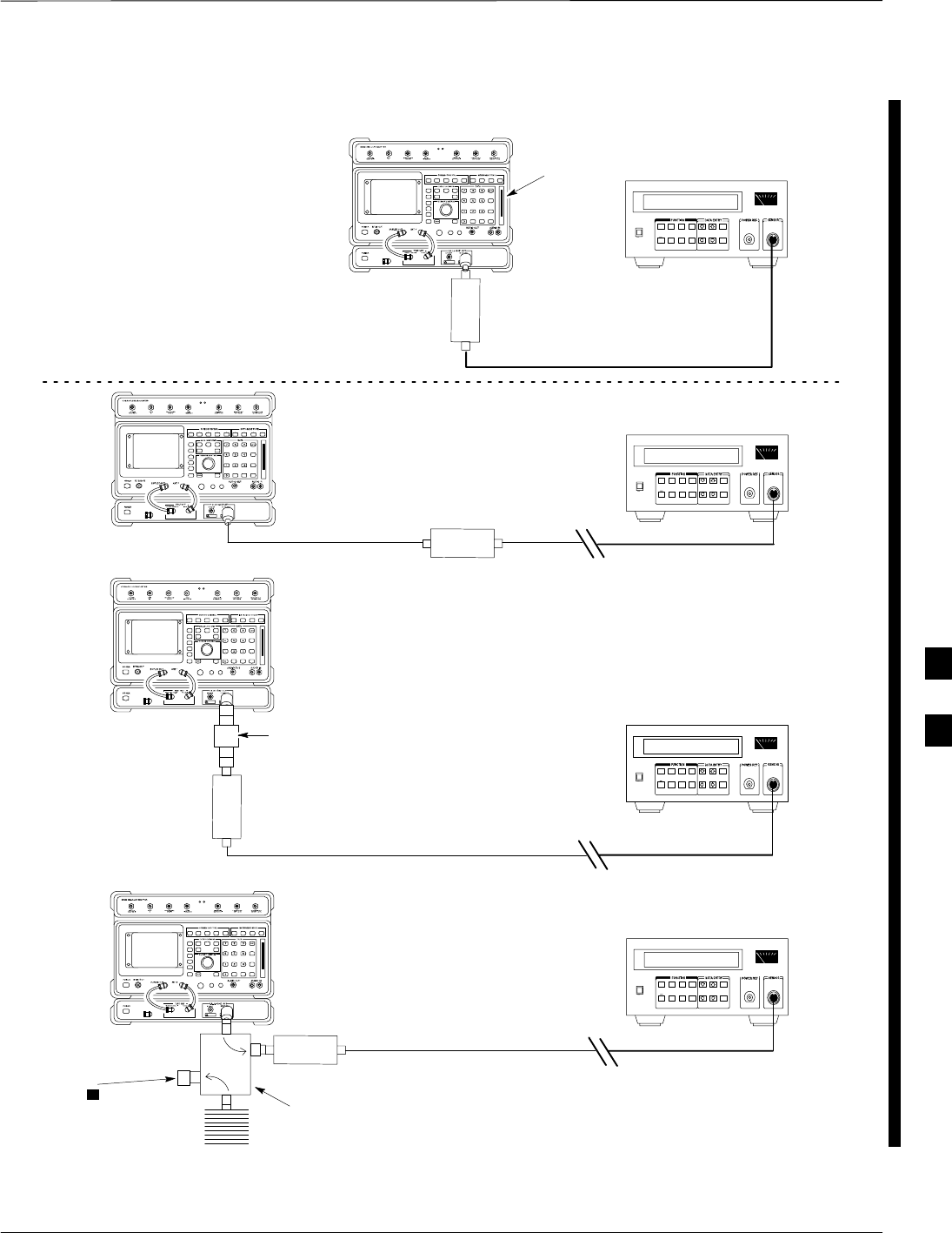
Manual Cable Calibration – continued
FEB 2005 1X SC 4812T Lite BTS Optimization/ATP F-39
PRELIMINARY
(A)
(C)
(A)
POWER
SENSOR
(C)
30 dB
DIRECTIONAL
COUPLER
150 W
NON–RADIATING
RF LOAD
POWER
SENSOR
(B)
POWER
SENSOR
(B)
MEMORY
CARD
SLOT
20dB / 20 WATT
ATTENUATOR
FW00292
50 Ω
TERMINATOR
POWER
SENSOR
Figure F-23: Cable Calibration using HP8921 with PCS Interface
F

Manual Cable Calibration – continued
F-40 1X SC 4812T Lite BTS Optimization/ATP FEB 2005
PRELIMINARY
Calibrating the Test Cable
Set–up with the Advantest
R3465
Ensure that the GPIB Interface is OFF for the duration of
this procedure.
IMPORTANT
*
Advantest R3465 Manual Test Set–up and Calibration must be
performed on both the TX and RX Frequencies.
Table F-24: Test Cable Set–up (using Advantest R3465) Calibration Procedure
nStep Action
* IMPORTANT
This procedure can only be performed after Test Equipment has been allowed to warm–up and
stabilize for a minimum of 60 minutes.
1Press the SHIFT and the PRESET Keys located below the display.
2Press the ADVANCE Key in the MEASUREMENT area of the Control Panel.
3Select the CDMA Sig CRT Menu Key.
4Select the Set–up CRT Menu Key.
5Use the Vernier Knob and the Cursor Keys to set the following parameters.
Generator Mode: SIGNAL
Link: FORWARD
Level Unit: dBm
CalCorrection: ON
Level Offset: OFF
NOTE
Fields not listed remain at default values.
6Select the Return CRT Menu Key.
7 Press FREQ Key in the ENTRY Area.
8Set the Frequency to the desired value by using the Keypad Entry Keys.
9Verify that the Mod CRT Menu Key highlighting is OFF.
SIf it is highlighting OFF, proceed to Step 10.
SIf it is not highlighting OFF:
– Press the Mod Key to toggle it OFF.
–Proceed to Step 10.
table continued on next page
F

Manual Cable Calibration – continued
FEB 2005 1X SC 4812T Lite BTS Optimization/ATP F-41
PRELIMINARY
Table F-24: Test Cable Set–up (using Advantest R3465) Calibration Procedure
nActionStep
10 Verify that the Output CRT Menu Key highlighting is OFF.
SIf it is highlighting OFF, proceed to Step 11.
SIf it is not highlighting OFF:
– Press the Output Key to toggle it OFF.
–Proceed to Step 11.
11 Press the LEVEL Key in the ENTRY Area.
12 Set the LEVEL to 0 dBm using the Keypad Entry Keys.
13 Zero the Power Meter.
14 Connect the Power Sensor directly to the “RF OUT” Port on the R3561L CDMA Test Source Unit.
15 Press the Output CRT Menu Key to toggle Output to ON.
16 Record the Power Meter Reading ________________________
17 Disconnect the Power Meter Sensor from the R3561L RF OUT Jack.
* IMPORTANT
The Power Meter Sensor’s lower limit is –30dBm. Thus, only components having losses < 30 dB
should be measured using this method.
For best accuracy, always re–Zero the Power Meter before connecting the Power Sensor to
the component being calibrated.
–Then, after connecting the Power Sensor to the component, record the calibrated Loss
immediately.
18 Disconnect all components in the the Test Set–up in order to calibrate each one separately.
18a Connect each component one–at–a–time between the “RF OUT” Port and the Power Sensor.
– Refer to Figure F-24, “Set–ups A, B, and C”.
18b Record the calibrated Loss Value displayed on the Power Meter for each connection.
Example: (A) 1st Test Cable = –0.5 dB
(B) 2nd Test Cable = –1.4 dB
(C) 20dB Attenuator = –20.1 dB
(D) 30 dB Directional Coupler = –29.8 dB
19 Press the Output CRT Menu Key to toggle Output OFF.
20 Calculate the total Test Set–up loss by adding up all the individual losses:
Example: Total Test Set–up loss = 0.5 + 1.4 + 20.1 + 29.8 = 51.8 dB
This calculated value will be used in the next series of tests.
21 Press the FREQ Key in the ENTRY Area.
22 Using the Keypad Entry Keys, set the test frequency to the RX Frequency.
table continued on next page
F
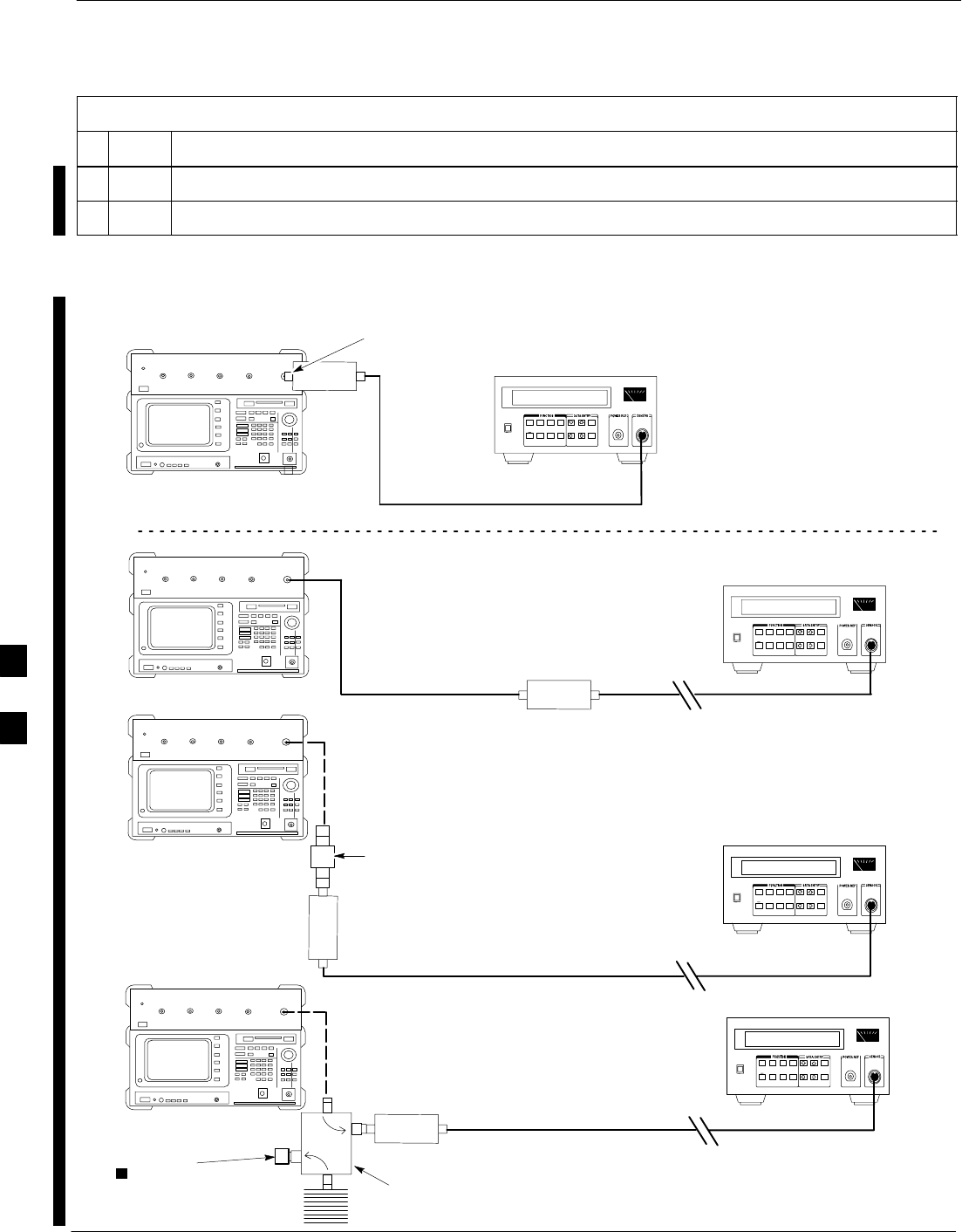
Manual Cable Calibration – continued
F-42 1X SC 4812T Lite BTS Optimization/ATP FEB 2005
PRELIMINARY
Table F-24: Test Cable Set–up (using Advantest R3465) Calibration Procedure
nActionStep
23 Repeat Steps 9 through 19 for the RX Frequency.
24 Refer to Chapter 3 for assistance in setting the Test Cable Insertion Loss Values into the LMF.
POWER
SENSOR
20 DB / 2 WATT
ATTENUATOR
(A)
(C)
POWER
SENSOR
(D)
30 DB
DIRECTIONAL
COUPLER
(C)
100 W
NON–RADIATING
RF LOAD
POWER
SENSOR
RF OUT
POWER
SENSOR
& (B)
FW00320
50 Ω
TERMINATOR
Figure F-24: Cable Calibration using the Advantest R3465
F


Table of Contents – continued
1X SC 4812T Lite BTS Optimization/ATP FEB 2005
PRELIMINARY
Notes
G

Downloading ROM Code
FEB 2005 1X SC 4812T Lite BTS Optimization/ATP G-1
PRELIMINARY
Exception Procedure –
Downloading ROM Code
This procedure is not part of a normal Optimization.
Perform this procedure only on an exception basis when no alternative
exists to load a BTS Device with the correct version of ROM Code.
One GLI must be INS_ACTIVE (bright green) before
ROM Code can be downloaded to non–GLI Devices.
NOTE
The correct ROM and RAM Codes for the Software
Release used on the BSS must be loaded into BTS
Devices. To identify the correct device ROM and RAM
Code Loads for the Software Release being used on the
BSS, refer to the Version Matrix section of the SCt
CDMA Release Notes (supplied on the tapes or
CD–ROMs containing the BSS Software).
All devices in a BTS must be loaded with the ROM and
RAM Code specified for the Software Release used on the
BSS before any Optimization or Acceptance Test
Procedures can be performed.
If a replacement device is loaded with ROM Code that is
not compatible with the BSS Software Release being used,
the Device ROM Code can be changed using the LMF
before performing the BTS Optimization and ATPs. A
device loaded with later release ROM Code can not be
converted back to a previous release ROM Code in the
field without Motorola assistance.
CAUTION
If it is necessary to download ROM Code to a device from the LMF, the
procedure in Table G-1 includes steps for both ROM and RAM Code
download using the LMF.
Prerequisites
Prior to performing this procedure, ensure the correct ROM and RAM
Code Files exist in the LMF Computer’s applicable <x>:\<lmf home
directory>\cdma\loads\<codeload#>\code Folder for each of the
devices to be loaded.
G

Downloading ROM Code – continued
G-2 1X SC 4812T Lite BTS Optimization/ATP FEB 2005
PRELIMINARY
The Release Level of the ROM Code to be downloaded
must be the one specified for the Software Release
installed in the BSS. The Release Level of the ROM Code
resident in the other devices in the BTS must also be
correct for the BSS Software Release being used.
ROM Code must not be downloaded to a frame loaded
with code for a BSS Software Release with which it is not
compatible.
This procedure should only be used to upgrade
replacement devices for a BTS. It should NOT be used to
upgrade all devices in a BTS.
If a BTS is to be upgraded from R15.x to R16.0, etc., the
upgrade should be done by the OMC–R using the
DownLoad Manager.
CAUTION
Table G-1: ROM and RAM Code Download to Devices Procedure
nStep Action
1Click on the device to be loaded.
NOTE
More than one device of the same type can be selected for download by either clicking on each
one to be downloaded or from the BTS Menu Bar Select Pull–down Menu, select the device item
that applies.
Where: device = the type of device to be loaded (BBX, CSM, GLI, MCC)
2From the BTS Menu Bar Device Pull–down Menu, select Status.
– A Status Report Window will appear.
3Make a note of the number in the HW Bin Type column.
NOTE
“HW Bin Type” is the Hardware Binary Type for the device. This code is used as the last four
digits in the filename of a device’s Binary ROM Code File.
– By using this part of the filename, the ROM Code File can be matched to the device in which
it is to be loaded.
4 Click OK to close the Status Window.
5Click on the device to be loaded.
NOTE
ROM Code is automatically selected for download from the <x>:\<lmf Home
Directory>\version folder>\<Code Folder> specified by the NextLoad property
in the bts–#.CDF File.
To check the value of the NextLoad Property, click on Util > Examine > Display NextLoad.
– A Pop–up Message will show the value of the NextLoad.
table continued on next page
G

Downloading ROM Code – continued
FEB 2005 1X SC 4812T Lite BTS Optimization/ATP G-3
PRELIMINARY
Table G-1: ROM and RAM Code Download to Devices Procedure
nActionStep
6From the BTS Menu Bar Device Pull–down Menus, select Download > ROM.
SIf the file matching the Hardware Binary Type of the device is found in the Code Folder, a
Status Report shows the result of the download.
–Proceed to Step 11.
SIf a file selection Window appears, select the ROM Code File manually.
–Proceed to Step 7.
7Double–click on the Version Folder with the desired Version Number for the ROM Code File (for
example: 2.16.0.x).
8Double–click the Code Folder.
– A list of ROM and RAM Code Files will be displayed.
9! CAUTION
A ROM Code File with the correct HW Bin Type must be chosen. Using a file with the wrong
HW Bin Type can result in unpredictable operation and damage to the device.
Click on the ROM Code File with the filename that matches the device type and HW Bin Type
number noted in Step 3 (for example, file bbx_rom.bin.0604 is the ROM Code File for a BBX
with a HW Bin Type of 0604).
– The file should be highlighted.
10 Click on the Load Button.
– A Status Report Window is displayed showing the result of the download.
NOTE
If the ROM Load failed for some devices, load them individually by clicking on one device,
perform Steps 6 through 10 for it, and repeat the process for each remaining device.
11 Click OK to close the Status Window.
12 From the LMF Window Menu Bar Tools Pull–down Menus, select Update NextLoad > CDMA.
13 In the left–hand pane of the window that opens, click on the BTS Number for the frame being
loaded (for example, BTS–14).
14 On the list of versions displayed in the right–hand pane, click the Button next to the Version
Number of the folder that was used for the ROM Code download (for example, 2.16.0.x) and click
Save.
– A Pop–up Message will appear showing the CDF has been updated.
15 Click on the OK Button to dismiss the Pop–up Message.
16 Click on the device that was loaded with ROM Code.
table continued on next page
G

Downloading ROM Code – continued
G-4 1X SC 4812T Lite BTS Optimization/ATP FEB 2005
PRELIMINARY
Table G-1: ROM and RAM Code Download to Devices Procedure
nActionStep
17 NOTE
RAM Code is automatically selected for download.
From the BTS Menu Bar Device Pull–down Menus, select Download > Code/Data to download
RAM Code and DDS File Data.
– A Status Report is displayed showing the result of the download.
18 Click OK to close the Status Window.
19 Observe the downloaded non–GLI Device to ensure it is OOS_RAM (yellow).
20 Click on the device that was loaded with code.
21 From the BTS Menu Bar Device Pull–down Menu, select Status.
Verify that the correct ROM and RAM Version Numbers are displayed in the Status Report
Window.
22 Click OK to close the Status Window.
G

FEB 2005 1X SC 4812T Lite BTS Optimization/ATP
PRELIMINARY
Appendix H: In–Service Calibration
Appendix Content
Introduction H-1 . . . . . . . . . . . . . . . . . . . . . . . . . . . . . . . . . . . . . . . . . . . . . . . . . . . . .
Purpose H-1 . . . . . . . . . . . . . . . . . . . . . . . . . . . . . . . . . . . . . . . . . . . . . . . . .
Equipment STabilization and Calibration H-1 . . . . . . . . . . . . . . . . . . . . . . .
1X Test Equipment Requirements H-1 . . . . . . . . . . . . . . . . . . . . . . . . . . . . .
Power Delta Calibration H-3 . . . . . . . . . . . . . . . . . . . . . . . . . . . . . . . . . . . . . . . . . . .
Introduction H-3 . . . . . . . . . . . . . . . . . . . . . . . . . . . . . . . . . . . . . . . . . . . . . .
Agilent E4406A Power Delta Calibration H-3 . . . . . . . . . . . . . . . . . . . . . . .
Advantest R3267 Power Delta Calibration H-6 . . . . . . . . . . . . . . . . . . . . . .
Agilent 8935 Series E6380A Power Delta Calibration H-9 . . . . . . . . . . . . .
HP 8921A Power Delta Calibration H-12 . . . . . . . . . . . . . . . . . . . . . . . . . . .
Advantest R3465 Power Delta Calibration H-14 . . . . . . . . . . . . . . . . . . . . . .
In–Service Calibration H-19 . . . . . . . . . . . . . . . . . . . . . . . . . . . . . . . . . . . . . . . . . . . .
In–Service Calibration H-19 . . . . . . . . . . . . . . . . . . . . . . . . . . . . . . . . . . . . . .
H

Table of Contents – continued
1X SC 4812T Lite BTS Optimization/ATP FEB 2005
PRELIMINARY
Notes
H

Introduction
FEB 2005 1X SC 4812T Lite BTS Optimization/ATP H-1
PRELIMINARY
Purpose
This procedure is a guide to performing Calibration of new BTS
expansion carriers while the system remains in service. This procedure
also supports BTS Recalibration following replacement of RF Chain
components while the remainder of the site stays in service.
Motorola recommends performing this procedure during a Maintenance
Window.
This procedure cannot be performed on BTSs with 2–to–1 Combiners.
The procedure can only be performed on one carrier of the BTS at a
time. That is, LPA Modules 1A, 1B, 1C, and 1D can be calibrated while
LPA Modules 3A, 3B, 3C, and 3D remain in service and vice versa.
Equipment STabilization and
Calibration
Calibration of the Communications Test Set (or equivalent
Test Equipment) must be performed at the site before
calibrating the overall Test Equipment Set.
Calibrate the Test Equipment after it has been allowed to
warm-up and stabilize for a minimum of 60 minutes.
NOTE
If any component of the Test Equipment Set (for example,
a Test Cable, RF Adapter, Signal Generator) has been
replaced, the Test Equipment Set must be recalibrated.
Failure to do so could introduce Measurement Errors that
ultimately result in degradation of system performance.
CAUTION
1X Test Equipment
Requirements
In–Service Calibration (ISC) of 1X carrier functions requires using the
following Test Equipment for the purposes indicated:
SAn Advantest R3267 Spectrum Analyzer to perform TX Calibration.
SAn Advantest R3562 Signal Generator for R3267 Delta Power
Calibration.
SAn Agilent E4406A Transmitter Test Set to perform TX Calibration
SAn Agilent E4432A Signal Generator for E4406A Delta Power
Calibration.
SAn Agilent 8935 Series E6380A equipped with Option 200 (if
purchased new) or option R2K (if retrofitted) to perform TX
Calibration.
H

Introduction – continued
H-2 1X SC 4812T Lite BTS Optimization/ATP FEB 2005
PRELIMINARY
The CDMA Communications System Analyzers listed above are capable
of calibrating the BTS for both IS–95 A and B Mode Operation as well
as CDMA2000 1X Operation.
IS–95A/B Communication Test Sets such as the HP
8921A/600 and Advantest R3561L can not calibrate 1X
carrier functions.
NOTE
Calibration and Test Set–up for the HP 8921A/600 and Advantest
R3561L Test Sets is included only for situations where it is necessary to
use them for Calibration of IS–95A/B Mode Operation.
H

Power Delta Calibration
FEB 2005 1X SC 4812T Lite BTS Optimization/ATP H-3
PRELIMINARY
Introduction
The ISC Procedure has several differences from a normal Calibration
Procedure. One of these is the use of a Spectrum
Analyzer/Communications Test Set instead of a Power Meter to measure
power.
– Power Meters are Broadband Measurement Devices and cannot be
used to measure power during ISC because other carriers are
operating.
– A Spectrum Analyzer can be used because it measures power at a
given frequency.
Measuring power using a Spectrum Analyzer is less accurate than using
a Power Meter, therefore, compensation is required for the Accuracy
Difference (Delta) between the Power Meter and the Spectrum Analyzer.
Agilent E4406A Power Delta
Calibration
The Agilent E4406A Transmitter Tester and E4432B Signal Generator
Test Equipment combination can be used for ISC of IS–2000 CDMA 1X
as well as IS–95A/B Operation Modes. The Power Delta Calibration is
performed on the E4406A, but the E4432B is required to generate the
Reference Signal used to calculate the Power Delta offset. After the
Offset Value has been calculated, add it to the TX Test Cable Insertion
Loss Value in the LMF.
Preliminary Agilent Test Equipment Set–up
To provide proper operation during Power Delta Calibration, ensure that
the E4406A and E4432B are connected as shown in Figure F-18.
Power Delta Calibration
Perform the procedure in Table H-1 to perform the Agilent E4406A
Power Delta Calibration Procedure.
Table H-1: Agilent E4406A Power Delta Calibration Procedure
nStep Action
NOTE
Perform this procedure after Test Equipment has been allowed to warm–up and stabilize for a
minimum of 60minutes.
– After it is warmed–up and stabilized, calibrate the Test Equipment as described in the “Test
Set Calibration” section of Chapter 3.
1Zero the Power Meter prior to connecting the Power Sensor to the RF Cable from the Signal
Generator.
NOTE
For best accuracy, always re–Zero the Power Meter before connecting the Power Sensor to the
component being calibrated.
table continued on next page
H

Power Delta Calibration – continued
H-4 1X SC 4812T Lite BTS Optimization/ATP FEB 2005
PRELIMINARY
Table H-1: Agilent E4406A Power Delta Calibration Procedure
nActionStep
2Ensure that the E4406A and E4432B are connected as shown in Figure F-18.
3Connect a short RF Cable from the E4432B RF OUTPUT Connector the HP437 Power Meter
Power Sensor.
– Refer to Figure H-1.
4Set the E4432B Signal Generator by performing the following actions.
4a Press Preset to exit any modes for which the Signal Generator is configured.
4b Press Frequency and enter the frequency of the channel to be calibrated on the Numeric Keypad.
4c Using the Softkeys to the right of the screen, select the Frequency Range to be measured; for
example: MHz.
4d Press Amplitude and, using the Numeric Keypad, set the Signal Amplitude to 0 (zero).
4e Using the Softkeys, set the measurement type to dBm.
5On the E4432B, press RF On/Off to toggle the RF Output to RF ON.
– Note that the RF On/Off Status in the Screen Display changes.
6Measure and record the Value Reading on the HP437 Power Meter as result.
A____________________
7On the E4432B, press RF On/Off to toggle the RF Output to RF OFF.
– Note that the RF On/Off Status in the Screen Display changes.
8Disconnect the short RF Cable from the HP437 Power Meter Power Sensor, and connect it to the
RF INPUT Connector on the E4406A Transmitter Tester.
– Refer to Figure H-2.
* IMPORTANT
Do not change the Frequency and Amplitude Settings on the E4432B when performing the
following actions.
9Set the E4406A by performing the following actions.
9a Press Preset to exit any modes for which the Transmitter Tester is configured.
9b Press MODE and, using the Softkeys to the right of the screen, select cdmaOne.
9c Press MEASURE and, using the Softkeys, select spectrum.
9d Press Frequency and, using the Softkeys, select Center Frequency.
9e Enter the frequency of the channel to be calibrated using the Numeric Keypad.
9f Using the Softkeys, select the Frequency Range to be measured; for example, MHz.
9g Press Input/Output and, using the Softkeys, select Input Atten.
9h Using the Numeric Keypad, set Input Atten to 0 (zero) and, using the Softkeys, select dB.
table continued on next page
H

Power Delta Calibration – continued
FEB 2005 1X SC 4812T Lite BTS Optimization/ATP H-5
PRELIMINARY
Table H-1: Agilent E4406A Power Delta Calibration Procedure
nActionStep
9i Using the Softkeys, select External Atten and then select Mobile.
9j Using the Numeric Keypad, set Mobile to 0 (zero) and, using the Softkeys, select dB.
9k Using the Softkeys, select Base.
9l Using the Numeric Keypad, set Base to 0 (zero) and, using the Softkeys, select dB.
9m Press MEASURE and, using the Softkeys, select Channel Power.
10 On the E4432B Signal Generator, press RF On/Off to toggle the RF Output to RF ON.
– Note that the RF On/Off status in the Screen Display changes.
11 Read the measured Channel Power from the E4406A Screen Display and record it as Result B.
B____________________.
12 On the E4432B, press RF On/Off to toggle the RF Output to RF OFF.
– Note that the RF On/Off status in the Screen Display changes.
13 Calculate the Power Calibration Delta Value.
– The Delta Value is the Power Meter Measurement minus the Agilent measurement.
Delta = A – B
Example: Delta = –0.70 dBm – (–1.25 dBm) = 0.55 dBm
Example: Delta = 0.26 dBm – 0.55 dBm = –0.29 dBm
NOTE
These examples are included to show the mathematics and do not represent actual readings.
NOTE
Add this Delta Value to the TX Cable Loss Value during In–Service Calibration.
– Refer to Step 4 in Table H-6.
Power
Sensor
Agilent E4432B and E4406A
Short RF Cable
HP437B
SENSOR
RF OUTPUT
Figure H-1: Delta Calibration Set–up – Agilent E4432B to HP437
H
Power Delta Calibration – continued
H-6 1X SC 4812T Lite BTS Optimization/ATP FEB 2005
PRELIMINARY
Short RF Cable
RF INPUT
Agilent E4432B and E4406A
RF OUTPUT
Figure H-2: Delta Calibration Set–up – Agilent E4432B to Agilent E4406A
H

Power Delta Calibration – continued
FEB 2005 1X SC 4812T Lite BTS Optimization/ATP H-7
PRELIMINARY
Advantest R3267 Power Delta
Calibration
The Advantest R3267 Spectrum Analyzer and R3562 Signal Generator
Test Equipment combination can be used for ISC of IS–2000 CDMA 1X
as well as IS–95A/B Operation Modes. The Power Delta Calibration is
performed on the R3267. After the Offset Value has been calculated, add
it to the TX Test Cable Insertion Loss Value.
Preliminary Advantest Test Equipment Set–up
To provide proper operation during Power Delta Calibration, ensure that
the R3267 is connected to the R3562 as shown in Figure F-19.
Power Delta Calibration
Perform the procedure in Table H-2 to perform the Advantest R3267
Power Delta Calibration Procedure.
Table H-2: Advantest R3267 Power Delta Calibration Procedure
nStep Action
NOTE
Warm-up Test Equipment for a minimum of 60 minutes prior to this procedure.
– After it is warmed–up and stabilized, calibrate the Test Equipment as described in the “Test
Set Calibration” section of Chapter 3.
1Ensure that the R3267 and R3562 are connected as shown in Figure F-19.
2Press the SHIFT and the PRESET Keys located on the right side of the Control Panel.
3Press the ADVANCE Key in the MEASUREMENT Area of the Control Panel.
4On the CRT, select RX Control by pressing ACTIVE Key 1.
5On the CRT, select Frequency Set–up by pressing ACTIVE Key 3.
6On the CRT, highlight Frequency by adjusting the DISPLAY CONTROL Knob.
7 Press FREQ Key in the ENTRY Section of the Control Panel.
8Set the frequency to the desired value using the Keypad ENTRY Section Keys.
9Press the LEVEL Key in the ENTRY Section of the Control Panel.
10 Set the level to 0 dBm using the Keypad ENTRY Section Keys.
11 On the CRT, verify OFF is highlighted in Modulation.
– If OFF is not highlighted, press the ACTIVE Key 5 to toggle it OFF.
12 On the CRT, verify OFF is highlighted in Output.
– If OFF is not highlighted, press the ACTIVE Key 6 to toggle it OFF.
table continued on next page
H

Power Delta Calibration – continued
H-8 1X SC 4812T Lite BTS Optimization/ATP FEB 2005
PRELIMINARY
Table H-2: Advantest R3267 Power Delta Calibration Procedure
nActionStep
13 Zero the Power Meter prior to connecting the Power Sensor to the RF Cable from the Signal
Generator.
NOTE
For best accuracy, always re–Zero the Power Meter before connecting the Power Sensor to the
component being calibrated.
14 Connect the RF Cable from the R3562 Signal Generator RF OUT Port to the Power Sensor.
15 On the R3562 CRT, set the Output to ON by pressing ACTIVE Key 6.
16 Record the Power Meter Reading as result A.
A________________________
17 On the R3562 CRT, set the Output to OFF by pressing ACTIVE Key 6.
18 Connect the RF Cable from R3562 Signal Generator RF OUT Port to the R3267 Spectrum
Analyzer INPUT Port.
– Refer to Figure H-4.
19 On the R3562 CRT, set the Output to ON by pressing ACTIVE Key 6.
20 On the R3267, press the POWER Key in the MEASUREMENT Area of the Control Panel.
21 Press the LEVEL Key in the ENTRY Section of the Control Panel.
22 Set the REF LEVEL to 10 dBm using the Keypad ENTRY Section Keys.
23 On the CRT, select dB/div by pressing ACTIVE Key 1.
24 On the CRT, select 10 dB/div by pressing ACTIVE Key 1.
25 Press the FREQ Key in ENTRY Section of the Control Panel.
26 Set the frequency to the desired value using the Keypad ENTRY Section Keys.
27 On the CRT, select more 1/2 by pressing ACTIVE Key 7.
28 Press the Preselector CRT Menu Key to highlight 3.66G.
29 Press the POWER Key in the MEASUREMENT Area of the Control Panel.
30 Press the SPAN Key in the ENTRY Section of the Control Panel.
31 On the CRT, select Zero Span by pressing ACTIVE Key 2.
32 Press the COUPLE Key in the ENTRY Section of the Control Panel.
33 On the CRT, select RBW and highlight MNL by pressing ACTIVE Key 3.
34 Set RBW to 30 kHz using Keypad ENTRY Section Keys.
35 On the CRT, select VBW and highlight MNL by pressing ACTIVE Key 2.
36 Set VBW to 1 MHz using Keypad ENTRY Section Keys.
table continued on next page
H
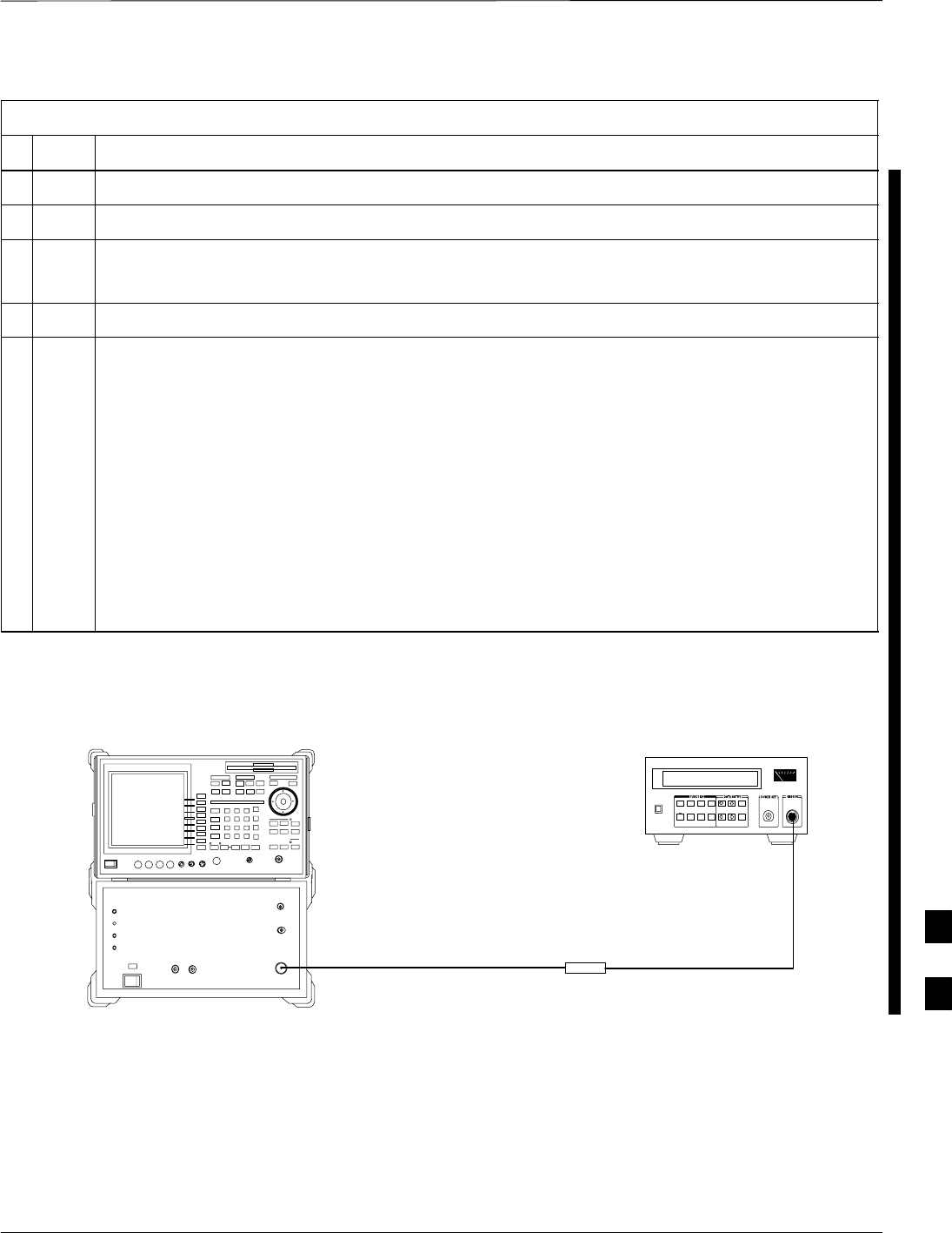
Power Delta Calibration – continued
FEB 2005 1X SC 4812T Lite BTS Optimization/ATP H-9
PRELIMINARY
Table H-2: Advantest R3267 Power Delta Calibration Procedure
nActionStep
37 Press the MKR Key in the DISPLAY CONTROL section of the Control Panel.
38 On the CRT, select Normal Marker by pressing ACTIVE Key 1.
39 Record the Marker Level reading as Result B.
B________________________
40 Press Single in ENTRY Section of Control Panel.
41 Calculate the Power Calibration Delta Value.
– The Delta Value is the Power Meter Measurement minus the Advantest Measurement.
Delta = A – B
Example: Delta = –0.7 dBm – (–1.25 dBm) = 0.55 dBm
Example: Delta = 0.26 dBm – 0.55 dBm = –0.29 dBm
NOTE
These examples are included to show the mathematics and do not represent actual readings.
NOTE
Add this Delta Value to the TX Cable Loss Value during In–Service Calibration.
– Refer to Step 4 in Table H-6.
Power
Sensor
Advantest R3562 and R3267
Short RF Cable
HP437B
SENSOR
RF OUT
Figure H-3: Delta Calibration Set–up – Advantest R3562 to HP437
H
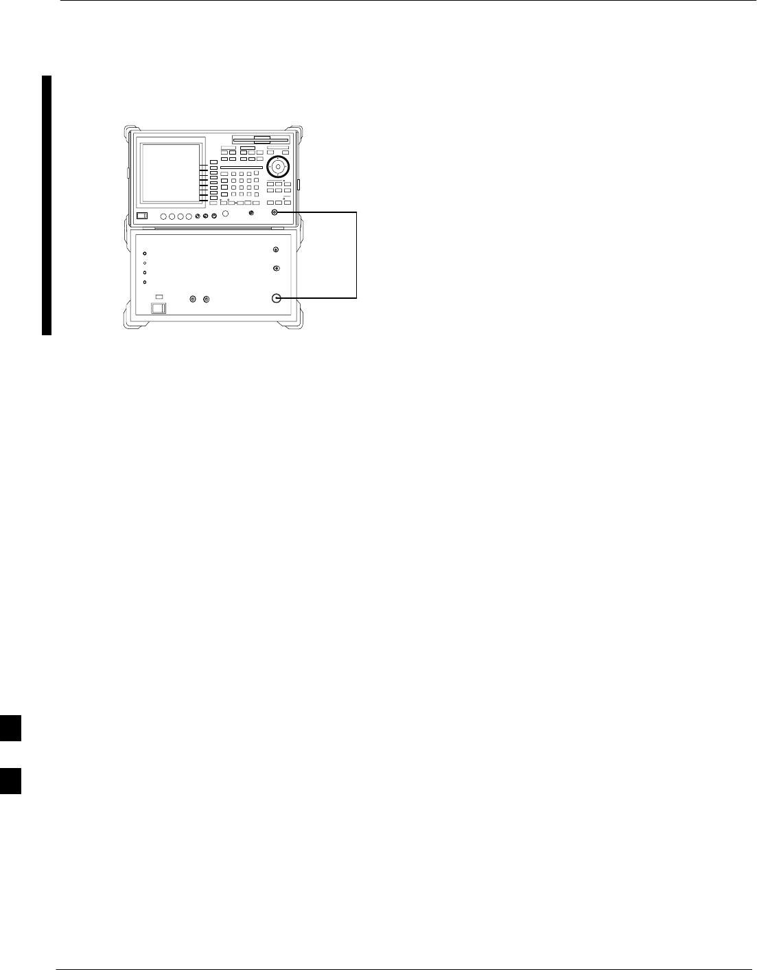
Power Delta Calibration – continued
H-10 1X SC 4812T Lite BTS Optimization/ATP FEB 2005
PRELIMINARY
Advantest R3562 and R3267
Short RF Cable
RF OUT
RF IN
Figure H-4: Delta Calibration Set–up – Advantest R3562 to R3267
H

Power Delta Calibration – continued
FEB 2005 1X SC 4812T Lite BTS Optimization/ATP H-11
PRELIMINARY
Agilent 8935 Series E6380A
Power Delta Calibration
The Agilent 8935 (formerly HP 8935) Communications Test Set
modified with either Option 200 or R2K and E4432B Signal Generator
Test Equipment combination can be used for ISC of IS–2000 CDMA 1X
as well as IS–95A/B Operation Modes. The Power Delta Calibration is
performed on the Agilent 8935. After the Offset Value has been
calculated, add it to the TX Test Cable Insertion Loss Value.
Perform the procedure in Table H-3 to perform the Agilent 8935 Power
Delta Calibration Procedure.
Table H-3: Agilent 8935 Power Delta Calibration Procedure
nStep Action
NOTE
Perform this procedure after Test Equipment has been allowed to warm–up and stabilize for a
minimum of 60 minutes.
– After it is warmed–up and stabilized, calibrate the Test Equipment as described in the “Test
Set Calibration” section of Chapter 3.
1Zero the Power Meter prior to connecting the Power Sensor to the RF Cable from the Signal
Generator.
NOTE
For best accuracy, always re–Zero the Power Meter before connecting the Power Sensor to the
component being calibrated.
2Connect a short RF Cable between the Agilent 8935 Duplex Out port and the HP437 Power
Sensor.
– Refer to Figure H-5.
3Set the Agilent 8935 Signal Source as follows:
– Measure Mode to CDMA Gen
– Frequency to the CDMA Calibration Target Frequency
– CW RF Path to IQ
– Output Port to Dupl
– Data Source to Random
– Amplitude to 0 dBm
4Measure and record the Power Value Reading on the HP437 Power Meter.
5Record the Power Meter Reading as Result A.
A ________________________.
6Turn off the Agilent 8935 Signal Source Output, and disconnect the HP437.
NOTE
Leave the settings on the Source Agilent 8935 for convenience in the following steps.
table continued on next page
H

Power Delta Calibration – continued
H-12 1X SC 4812T Lite BTS Optimization/ATP FEB 2005
PRELIMINARY
Table H-3: Agilent 8935 Power Delta Calibration Procedure
nActionStep
7Connect the short RF Cable between the Agilent 8935 Duplex Out Port and the RF–IN/OUT Port.
– Refer to Figure H-6.
8Ensure that the Source Agilent 8935 Settings are the same as in Step 3.
9Set the Agilent 8935 as follows:
– Measure Mode to CDMA Anl
– Frequency to the CDMA Calibration Target Frequency
– Input Attenuation to 0 dB
– Input Port to RF–IN
– Gain to Auto
– Anl Dir to Fwd
10 Turn on the Agilent 8935 Signal Output.
11 Set the Chn Pwr Cal to Calibrate and select to calibrate.
12 Measure and record the Channel Power Reading on the measuring Agilent 8935 as Result B.
B ________________________
13 Turn off the Agilent 8935 Signal Output and disconnect the equipment.
14 Calculate the Power Calibration Delta Value.
– The Delta Value is the Power Meter Measurement minus the Advantest Measurement.
Delta = A – B
Example: Delta = –0.70 dBm – (–1.25 dBm) = 0.55 dBm
Example: Delta = 0.26 dBm – 0.55 dBm = –0.29 dBm
NOTE
These examples are included to show the mathematics and do not represent actual readings.
NOTE
Add this Delta Value to the TX Cable Loss Value during In–Service Calibration.
– Refer to Step 4 in Table H-6.
Power
Sensor
Agilent Agilent 8935
DUPLEX OUT Short RF Cable
HP437B
SENSOR
FW00805
Figure H-5: Delta Calibration Set–up – Agilent 8935 to HP437
H

Power Delta Calibration – continued
FEB 2005 1X SC 4812T Lite BTS Optimization/ATP H-13
PRELIMINARY
Agilent E6380A
Short RF Cable
DUPLEX OUT RF IN/OUT
FW00806
Figure H-6: Delta Calibration Set–up – Agilent 8935 to Agilent 8935
H

Power Delta Calibration – continued
H-14 1X SC 4812T Lite BTS Optimization/ATP FEB 2005
PRELIMINARY
HP 8921A Power Delta
Calibration
Use the HP 8921A Communications Test Set to measure power during
ISC only for IS–95A and B Operation of 800 MHz Systems. After the
Offset Value has been calculated, add it to the TX Test Cable Insertion
Loss Value.
Perform the procedure in Table H-4 to perform the HP 8921A Power
Delta Calibration Procedure.
This procedure requires two HP 8921A Communication
Test Sets.
NOTE
Table H-4: HP 8921A Power Delta Calibration Procedure
nStep Action
NOTE
Perform this procedure after Test Equipment has been allowed to warm–up and stabilize for a
minimum of 60 minutes. After it is warmed–up and stabilized, calibrate the Test Equipment as
described in the “Test Set Calibration” section of Chapter 3.
1Zero the Power Meter prior to connecting the Power Sensor to the RF Cable from the Signal
Generator.
NOTE
For best accuracy, always re–Zero the Power Meter before connecting the Power Sensor to the
component being calibrated.
2Connect a short RF Cable between the HP 8921A Duplex Out Port and the HP437 Power Sensor.
Refer to Figure H-7.
3Set the HP 8921A Signal Source as follows:
– Measure Mode to CDMA Generator
– Frequency to the CDMA Calibration Target Frequency
– CW RF Path to IQ
– Output Port to Dupl
– Data Source to Random
– Amplitude to 0 dBm
4Measure and record the Power Value Reading on the HP437 Power Meter.
5Record the Power Meter Reading as Result A.
A ________________________.
6Turn off the source HP 8921A Signal Output, and disconnect the HP437.
NOTE
Leave the settings on the source HP 8921A for convenience in the following steps.
table continued on next page
H

Power Delta Calibration – continued
FEB 2005 1X SC 4812T Lite BTS Optimization/ATP H-15
PRELIMINARY
Table H-4: HP 8921A Power Delta Calibration Procedure
nActionStep
7Connect the short RF Cable between the source HP 8921A Duplex Out Port and the measuring
HP 8921A RF–IN Port.
– Refer to Figure H-8.
8Ensure that the source HP 8921A Settings are the same as in Step 3.
9Set the measuring HP 8921A as follows:
– Measure Mode to CDMA Anl
– Frequency to the CDMA Calibration Target Frequency
– Input Attenuation to 0 dB
– Input Port to RF–IN
– Gain to Auto
– Analyzer Direction to Fwd
10 Turn on the source HP 8921A Signal Output.
11 Measure and record the Channel Power Reading on the measuring HP 8921A as Result B.
B ________________________
12 Turn off the source HP 8921A Signal Output and disconnect the equipment.
13 Compute the Delta between HP437 and HP 8921A using the following formula.
Delta = A – B
Example: Delta = –0.70 dBm – (–1.25 dBm) = 0.55 dBm
Example: Delta = 0.26 dBm – 0.55 dBm = –0.29 dBm
NOTE
These examples are included to show the mathematics and do not represent actual readings.
NOTE
Add this Delta Value to the TX Cable Loss Value during In–Service Calibration.
– Refer to Step 4 in Table H-6.
Short RF Cable
HP 8921A
DUPLEX
OUT
HP437B
Power
Sensor
SENSOR
FW00801
Figure H-7: Delta Calibration Set–up – HP 8921A to HP437
H
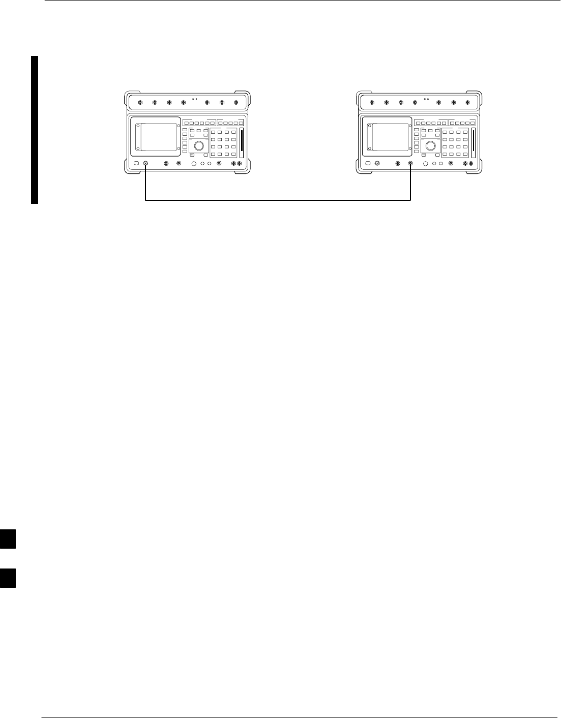
Power Delta Calibration – continued
H-16 1X SC 4812T Lite BTS Optimization/ATP FEB 2005
PRELIMINARY
Measurement HP 8921A Source HP 8921A
Short RF Cable
DUPLEX
OUT
RF
IN/OUT FW00802
Figure H-8: Delta Calibration Set–up – HP 8921A to HP 8921A
H

Power Delta Calibration – continued
FEB 2005 1X SC 4812T Lite BTS Optimization/ATP H-17
PRELIMINARY
Advantest R3465 Power Delta
Calibration
Use the Advantest R3465 Spectrum Analyzer to measure power during
ISC only for IS–95A and B Operation. After the Offset Value has been
calculated, add it to the TX Test Cable Insertion Loss Value.
Perform the procedure in Table H-5 to perform the Advantest 3465
Power Delta Calibration Procedure.
Table H-5: Advantest Power Delta Calibration Procedure
nStep Action
NOTE
Perform this procedure after Test Equipment has been allowed to warm–up and stabilize for a
minimum of 60 minutes.
– After it is warmed–up and stabilized, calibrate the Test Equipment as described in the “Test
Set Calibration” section of Chapter 3.
1Press the SHIFT and the PRESET Keys located below the CRT Display.
2Press the ADVANCE Key in the MEASUREMENT Area of the Control Panel.
3Press the CDMA Sig CRT Menu Key.
4Press the FREQ Key in the ENTRY Area of the Control Panel.
5Set the frequency to the desired value using the Keypad Entry Keys.
6Press the LEVEL Key in the ENTRY Area of the Control Panel.
7Set the LEVEL to 0 dBm using the Keypad Entry Keys.
8Verify that the Mod CRT Menu Key highlighting is OFF.
– If it is highlighted, press the Mod Key to toggle it OFF.
9Verify that the Output CRT Menu Key highlighting is OFF,
– If it is highlighted, press the Output Key to toggle it OFF.
10 Zero the Power Meter prior to connecting the Power Sensor to the RF Cable from the Signal
Generator.
NOTE
For best accuracy, always re–Zero the Power Meter before connecting the Power Sensor to the
component being calibrated.
11 Connect the RF Cable from the R3561L CDMA Signal Generator RF OUT Port to the Power Sensor.
– Refer to Figure H-9.
12 Press the Output CRT Menu Key to toggle the Output to ON.
13 Record the Power Meter Reading as Result A.
A________________________.
14 Press the Output CRT Menu Key to toggle the Output to OFF.
table continued on next page
H

Power Delta Calibration – continued
H-18 1X SC 4812T Lite BTS Optimization/ATP FEB 2005
PRELIMINARY
Table H-5: Advantest Power Delta Calibration Procedure
nActionStep
15 Connect the RF Cable from the R3561L Signal Generator RF OUT Port to the R3465 INPUT Port.
– Refer to Figure H-10.
16 Press the Output CRT Menu Key to change the Output to ON.
17 Press the CW Key in the MEASUREMENT Area of the Control Panel.
18 Press the LEVEL Key in the ENTRY Area of the Control Panel.
19 Set the REF LEVEL to 10 dBm using the Keypad Entry Keys.
20 Press the dB/div CRT Menu Key.
21 Press the 10 dB/div CRT Menu Key.
22 Press the FREQ Key in ENTRY Area of the Control Panel.
23 Set the frequency to the desired value using the Keypad Entry Keys.
24 Press the more 1/2 CRT Menu Key.
25 Press the Preselector CRT Menu Key to highlight 3.0G.
26 Press the FORMAT Key in the Display Control area of the Control Panel.
27 Press the TRACE CRT Menu Key.
28 Press the AVG A CRT Menu Key.
29 Set AVG to 20 using Keypad Entry Keys.
30 Press the return CRT Menu Key.
31 Press the SPAN Key in the ENTRY Area of the Control Panel.
32 Press the Zero Span CRT Menu Key.
33 Press the BW Key in the ENTRY Area of the Control Panel.
34 Press the RBW CRT Menu Key to highlight MNL. using Keypad Entry Keys enter 30 kHz.
35 Set RBW to 30 kHz using Keypad Entry Keys.
36 Press the VBW CRT Menu Key to highlight MNL.
37 Set VBW to 1 MHz using Keypad Entry Keys.
38 Press the Marker ON Key in the Display Control area of the Control Panel.
table continued on next page
H
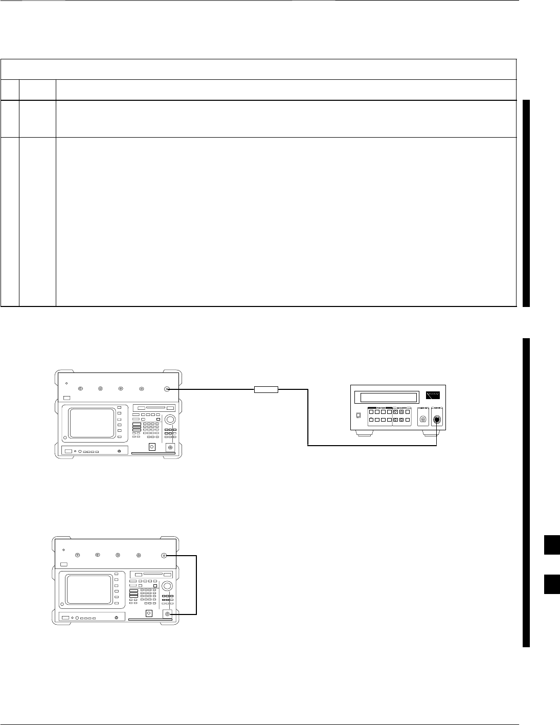
Power Delta Calibration – continued
FEB 2005 1X SC 4812T Lite BTS Optimization/ATP H-19
PRELIMINARY
Table H-5: Advantest Power Delta Calibration Procedure
nActionStep
39 Record the Marker Level reading as Result B.
B________________________
40 Calculate the Power Calibration Delta Value.
– The Delta Value is the Power Meter Measurement minus the Advantest Measurement.
Delta = A – B
Example: Delta = –0.70 dBm – (–1.25 dBm) = 0.55 dBm
Example: Delta = 0.26 dBm – 0.55 dBm = –0.29 dBm
NOTE
These examples are included to show the mathematics and do not represent actual readings.
NOTE
Add this Delta Value to the TX Cable Loss Value during In–Service Calibration. Refer to Step 4
in Table H-6.
Advantest Power
Sensor
RF OUT
Short RF Cable
HP437B
SENSOR
R3561L
FW00803
Figure H-9: Delta Calibration Set–up – R3561L to HP437
R3561L
RF OUT
INPUT
Short RF Cable
R3465
FW00804
Figure H-10: Delta Calibration Set–up – R3561L to R3465
Advantest
H

Power Delta Calibration – continued
H-20 1X SC 4812T Lite BTS Optimization/ATP FEB 2005
PRELIMINARY
Notes
H

In–Service Calibration
FEB 2005 1X SC 4812T Lite BTS Optimization/ATP H-21
PRELIMINARY
In–Service Calibration
This feature does NOT have Fault Tolerance at this time.
The system has no safe–guards to prevent actions that will
put the BTS out of service. If possible, perform this
procedure during a Maintenance Window.
Perform the procedures in this section precisely, otherwise
the entire BTS will most likely go OUT OF SERVICE.
At the CBSC, only perform operations on expansion
hardware when it is in the OOS_MANUAL State.
The operator must be trained in the LMF Operation prior
to performing this procedure.
CAUTION
Prerequisites
SAny applicable expansion hardware has been added in the CBSC
Database, and a CDF that includes the additions has been generated.
SAny expansion devices have been inserted into the SCCP Cage and
are in the OOS_MANUAL State at the CBSC MM.
SThe site specific CDF (with any expansion hardware) and CAL Files
have been loaded onto the LMF.
SThe LMF has the same Device Binary Code and DDS Files as the
CBSC.
Do not download code or data to any cards other than those
being worked on. Downloading code or data to other cards
will take the site OUT OF SERVICE.
The Code File Version Numbers must match the current
BSS Software Release Version Numbers required for the
equipped devices. If the numbers do not match, the site
may go OUT OF SERVICE.
It is mandatory that the bts–#.cdf and cbsc–#.CDF
Files on the LMF Computer for this BTS are copies of the
corresponding files created in the CBSC Database. Refer to
Table 3-3.
The CAL File loaded on the LMF Computer for this BTS
must have come from the CBSC.
CAUTION
H

In–Service Calibration – continued
H-22 1X SC 4812T Lite BTS Optimization/ATP FEB 2005
PRELIMINARY
STest Equipment has been connected as shown in Figure H-11 or
Figure H-12.
SAn RFDS (or as a minimum, a Directional Coupler), whose Loss is
already known, must be in the applicable TX Antenna Path to perform
the In–service Calibration.
STest Equipment has been calibrated after a 60–minute warm–up.
SA short RF Cable and two BNC–N Adapters are available to perform
Cable Calibration.
SN–SMA Cable Adapters are available to connect to TRDC or DRDC
BTS CPLD Connectors, and are included in Test Cable Insertion Loss
Measurements.
SThe Power Delta Calibration has been performed.
– Refer to Table H-1, Table H-2, Table H-3, Table H-4, or Table H-5.
H
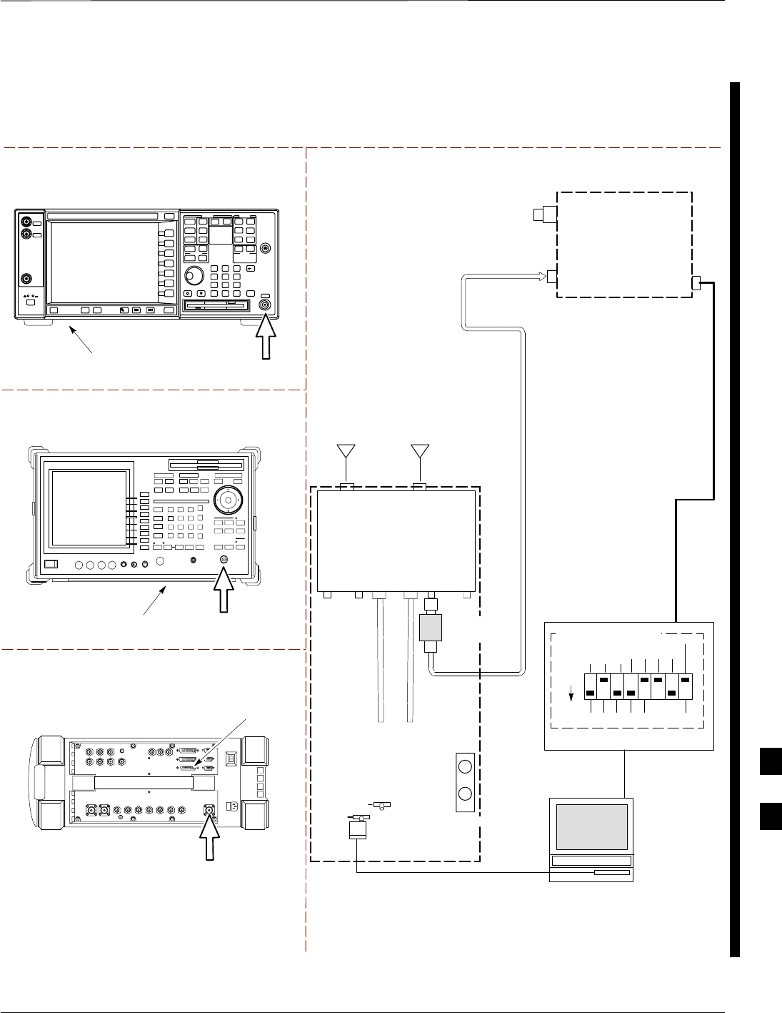
In–Service Calibration – continued
FEB 2005 1X SC 4812T Lite BTS Optimization/ATP H-23
PRELIMINARY
TEST SETS TRANSMIT (TX) SET–UP
TO
MPC
TO LPA
TRUNKING
MODULE
RS232–GPIB
INTERFACE BOX
INTERNAL PCMCIA
ETHERNET CARD
GPIB
CABLE
UNIVERSAL TWISTED PAIR (UTP)
CABLE (RJ45 CONNECTORS)
RS232 NULL
MODEM
CABLE
S MODE
DATA FORMAT
BAUD RATE
GPIB ADRS G MODE
ON
BTS
INTERNAL
TX
CABLE
CDMA
LMF
DIP SWITCH SETTINGS
10BASET/
10BASE2
CONVERTER
LAN
B
LAN
A
GPIB
RF INPUT 50Ω,
INPUT 50Ω,
OR RF IN/OUT
FREQ
MONITOR
SYNC
MONITOR
CSM
INTERNAL
RX
CABLE
TX
ANT
CPLD
RX
BTS
CPLD
TRDC
TX
BTS
CPLD
RX
ANT
CPLD
COMMUNICATIONS
SYSTEM ANALYZER
* BLACK RECTANGLES
REPRESENT THE RAISED
PART OF SWITCHES
NOTE: IF BTS IS EQUIPPED
WITH DRDCS (DUPLEXED
RX/TX SIGNALS), CONNECT
THE TX TEST CABLE TO
THE DRDC BTS CPLD
CONNECTOR.
RF INPUT
50 Ω
Agilent E4406A
INPUT 50 Ω
Advantest R3267
RX
ANTENNA
CONNECTOR
TX
ANTENNA
CONNECTOR
2O DB
IN–LINE
ATTENUATOR
ANTENNAANTENNA
Agilent 8935 Series E6380A (formerly HP 8935)
RF IN/OUT
HP–IB TO
GPIB
BOX
GPIB CONNECTS
TO BACK OF UNIT
GPIB CONNECTS
TO BACK OF UNIT
NOTE:
THE AGILENT 8935 MUST BE EQUIPPED WITH OPTION 200 OR R2K
TO PERFORM 1X TX TESTING .
Figure H-11: TX Calibration Test Set–up – Agilent E4406A, Advantest R3267, and Agilent 8935 with
Option 200 or R2K (IS–95A/B and 1X CDMA 2000)
H
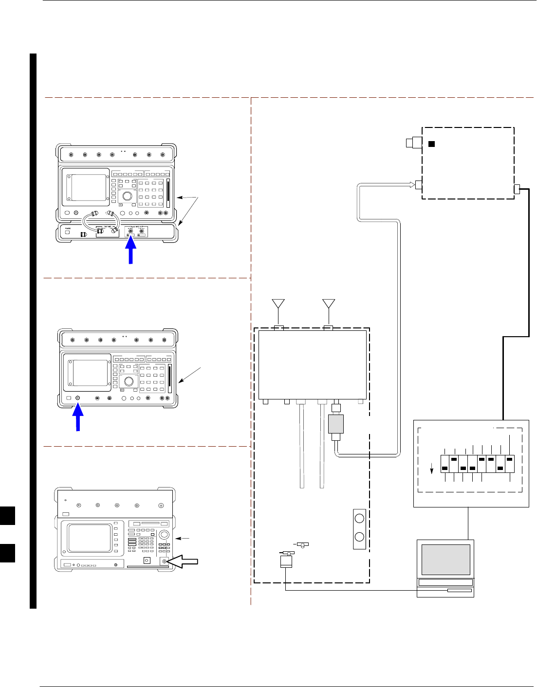
In–Service Calibration – continued
H-24 1X SC 4812T Lite BTS Optimization/ATP FEB 2005
PRELIMINARY
TEST SETS TRANSMIT (TX) SET–UP
TO
MPC
TO LPA
TRUNKING
MODULE
RS232–GPIB
INTERFACE BOX
INTERNAL PCMCIA
ETHERNET CARD
GPIB
CABLE
UNIVERSAL TWISTED PAIR (UTP)
CABLE (RJ45 CONNECTORS)
RS232 NULL
MODEM
CABLE
S MODE
DATA FORMAT
BAUD RATE
GPIB ADRS G MODE
ON
BTS
INTERNAL
TX
CABLE
CDMA
LMF
DIP SWITCH SETTINGS
10BASET/
10BASE2
CONVERTER
LAN
B
LAN
A
GPIB
RF IN/OUT
OR INPUT 50Ω
FREQ
MONITOR
SYNC
MONITOR
CSM
INTERNAL
RX
CABLE
TX
ANT
CPLD
RX
BTS
CPLD
TRDC
TX
BTS
CPLD
RX
ANT
CPLD
COMMUNICATIONS
SYSTEM ANALYZER
* BLACK RECTANGLES
REPRESENT THE RAISED
PART OF SWITCHES
NOTE: IF BTS IS EQUIPPED
WITH DRDCS (DUPLEXED
RX/TX SIGNALS), CONNECT
THE TX TEST CABLE TO
THE DRDC BTS CPLD
CONNECTOR.
RX
ANTENNA
CONNECTOR
TX
ANTENNA
CONNECTOR
2O DB
IN–LINE
ATTENUATOR
ANTENNAANTENNA
Hewlett Packard Model HP 8921A W/PCS Interface
(for 1900 MHz)
GPIB
CONNECTS
TO BACK OF
UNITS
RF
IN/OUT
GPIB
CONNECTS
TO BACK OF
UNIT
Hewlett Packard Model HP 8921A
(for 800 MHz)
RF
IN/OUT
Advantest Model R3465
INPUT 50Ω
GPIB CONNECTS
TO BACK OF UNIT
Figure H-12: TX Calibration Test Set–up – HP 8921A/600 w/PCS Interface (1.9 GHz),
HP 8921A/600 (800 MHz), and Advantest R3465 (IS–95A/B only)
H

In–Service Calibration – continued
FEB 2005 1X SC 4812T Lite BTS Optimization/ATP H-25
PRELIMINARY
Perform the procedure in Table H-6 to perform the In–Service
Calibration.
Table H-6: In–Service Calibration Procedure
nStep Action
NOTE
Perform this procedure after Test Equipment has been allowed to warm–up and stabilize for a
minimum of 60 minutes.
1Set–up the LMF for In–Service Calibration:
1a Start the LMF by double–clicking the LMF Icon on the Windows Desktop.
1b Click Tools > Options from the Menu Bar in the LMF Application Window.
1c In the LMF Options Window, check only the applicable Communications System Analyzer
Check Box on the Test Equipment Tab.
1d Ensure that the GPIB Address is 18.
1e Uncheck any other other equipment that is selected.
1f Click the Apply Button.
1g Select the BTS Options Tab in the LMF Options Window.
1h Check the In–Service Calibration Check Box.
1i Click the Apply Button.
1j Click the Dismiss Button to close the LMF Options Window.
2Log into the target BTS:
2a Select the target BTS Icon.
2b Click the Login Button at the Login Screen.
3Measure the Cable Loss using the Cable Calibration Function:
3a Click Util > Cable Calibration... in the BTS Menu Bar in the Main Window.
3b Set the desired Channel(s) and select TX and RX CABLE CAL from the Cable Calibration
Window Pull–down Menu.
3c Click the OK Button to perform Cable Calibration.
3d Follow the on–screen instructions to complete the Test Cable Insertion Loss Measurement.
NOTE
The measured value is input automatically to the Test Cable Insertion Loss File.
To view the Test Cable Insertion Loss File, click Util > Examine > Cable Loss from the BTS
Menu Bar.
table continued on next page
H

In–Service Calibration – continued
H-26 1X SC 4812T Lite BTS Optimization/ATP FEB 2005
PRELIMINARY
Table H-6: In–Service Calibration Procedure
nActionStep
4Add the Communications System Analyzer Power Delta to the TX Cable Loss.
4a In the BTS Menu Bar, click Util > Edit > Cable Loss... > TX.
4b Add the value computed in Table H-4, Table H-5, or Table H-3 to the TX Cable Loss.
NOTE
Ensure to include the sign of the value.
The following examples are included to show the mathematics and do not represent actual
readings:
– Example: 5.65 dBm + 0.55 dBm = 6.20dBm
– Example: 5.65 dBm + (–0.29 dBm) = 5.36 dBm
– Example: –5.65 dBm + 0.55 dBm = –5.10 dBm
– Example: –5.65 dBm + (–0.29 dBm) = –5.94 dBm
5Input the Coupler Loss for the TX Tests:
5a In the BTS Menu Bar, click Util > Edit > Coupler Loss... from the Menu Bar in the Main
Window.
5b Select the TX Coupler Loss Ta,b if not in the foreground.
5c Enter the appropriate Coupler Loss for the target carrier(s) by referring to the information taken at
the time of the BTS Installation.
5d Click the Save Button.
5e Click the Dismiss Button to close the window.
5f To view the Coupler Loss File, click Util > Examine > Coupler Loss in the BTS Menu Bar.
6Input the Coupler Loss for the RX Tests:
6a In the BTS Menu Bar, click Util > Edit > Coupler Loss... from the Menu Bar in the Main
Window.
6b Select the RX Coupler Loss Tab, if not in the foreground.
6c Enter the appropriate Coupler Loss for the target carrier(s) by referring to the information taken at
the time of the BTS Installation.
6d Click the Save Button.
6e Click the Dismiss Button to close the window.
6f To view the Coupler Loss File, click Util > Examine > Coupler Loss in the BTS Menu Bar.
table continued on next page
H

In–Service Calibration – continued
FEB 2005 1X SC 4812T Lite BTS Optimization/ATP H-27
PRELIMINARY
Table H-6: In–Service Calibration Procedure
nActionStep
7If it was not previously done, have the CBSC Operator put the Redundant BBX OOS_MANUAL.
! CAUTION
Be sure to download OOS devices only.
– Loading in–service devices takes them OUT OF SERVICE and can result in dropped calls.
The Code File Version Numbers must match the Version Numbers on the other cards in the frame.
If the numbers do not match, the site may go OUT OF SERVICE.
NOTE
Be sure to include the Redundant BBX in Steps 8, 9, and 10.
8Download code and data to the target devices:
8a In the LMF Window Menu Bar, click Tools > Update NextLoad > CDMA to set the Code
Version that will be downloaded.
8b Check the appropriate Code Version in the Pop–up Window and click the Save Button to close.
8c Select the target BBX(s) on the SCCP Cage picture.
8d In the BTS Menu Bar, click Device > Download > Code/Data to start downloading code and data.
! CAUTION
Perform the All Cal/Audit Procedure on OOS devices only.
9Run the All Cal/Audit Procedure:
9a Select the target BBX(s) on the SCCP Cage picture.
9b In the BTS Menu Bar, click Tests > All Cal/Audit... from the Menu Bar in the Main Window.
9c Select the target carrier and confirm the Channel Number in the Pop–up Window.
9d Leave the Verify BLO Check Box checked.
9e Ensure that the Test Pattern Box shows Pilot.
9f Click the OK Button to start Calibration.
9g Follow the on–screen instructions, except, do not connect to the BTS Antenna Port.
9h Connect to the DRDC or TRDC BTS CPL Port associated with the on–screen prompted Antenna
Port.
10 Save the result, and download the BLO Data to the target BBX(s):
– Click the Save Result Button on the result screen.
–– The window closes automatically.
11 Logout from the BTS and close the LMF Session:
11a In the BTS Menu Bar, click Select > Logout to close the BTS Connection.
11b Close the LMF Application Program by selecting File > Exit from the Window Menu Bar.
table continued on next page
H

In–Service Calibration – continued
H-28 1X SC 4812T Lite BTS Optimization/ATP FEB 2005
PRELIMINARY
Table H-6: In–Service Calibration Procedure
nActionStep
12 Disconnect all Test Cables from the BTS.
13 reconnect RFDS Cables or Termination Loads, as applicable, to the DRDC or TRDC BTS CPL
Ports used for the Calibration.
14 Advise the CBSC to enable the target device(s).
15 Restore the new “bts–*.cal” file to the CBSC.
– Refer to Table 4-12.
H

FEB 2005 1X SC 4812T Lite BTS Optimization/ATP
PRELIMINARY
Appendix I: Packet Backhaul Configuration
Appendix Content
BTS Router Initial Configuration I-1 . . . . . . . . . . . . . . . . . . . . . . . . . . . . . . . . . . . .
Overview I-1 . . . . . . . . . . . . . . . . . . . . . . . . . . . . . . . . . . . . . . . . . . . . . . . .
Terminal Setup I-2 . . . . . . . . . . . . . . . . . . . . . . . . . . . . . . . . . . . . . . . . . . . . . . . . . .
General I-2 . . . . . . . . . . . . . . . . . . . . . . . . . . . . . . . . . . . . . . . . . . . . . . . . . .
BTS Router Serial Communication I-4 . . . . . . . . . . . . . . . . . . . . . . . . . . . .
Downloading Minimum Canned BTS Router Configuration Files I-7 . . . . . . . . . .
Downloading Overview I-7 . . . . . . . . . . . . . . . . . . . . . . . . . . . . . . . . . . . . .
Prerequisites I-7 . . . . . . . . . . . . . . . . . . . . . . . . . . . . . . . . . . . . . . . . . . . . . .
FTP File Transfer from the OMC–R I-7 . . . . . . . . . . . . . . . . . . . . . . . . . . .
Verifying IOS Canned Version of the CF Memory Card I-13 . . . . . . . . . . . . . . . . . .
Overview I-13 . . . . . . . . . . . . . . . . . . . . . . . . . . . . . . . . . . . . . . . . . . . . . . . .
IOS Version Verification and File Sequence Position I-13 . . . . . . . . . . . . . .
Canned Configuration File Installation I-14 . . . . . . . . . . . . . . . . . . . . . . . . .
Method 1: Using a TFTP Server to Load to CF Memory Card I-15 . . . . . .
Method 2: Using a CF Memory Card Reader to Load
CF Memory Card I-31 . . . . . . . . . . . . . . . . . . . . . . . . . . . . . . . . . . . . . . . . .
Replacing Installed BTS Router CF Memory Card IOS Version I-41 . . . . . . . . . . . .
Background I-41 . . . . . . . . . . . . . . . . . . . . . . . . . . . . . . . . . . . . . . . . . . . . . .
Equipment and Software Required for Verification Methods I-41 . . . . . . . .
Required Publications I-41 . . . . . . . . . . . . . . . . . . . . . . . . . . . . . . . . . . . . . .
Method 1: Replacement of Installed Router CF Card IOS Data I-42 . . . . . .
Method 2: Using a CF Memory Card Reader for Replacement of
Installed IOS Version and Changing File Sequence Position I-50 . . . . . . .
Change CF Memory Card File Sequence to Place IOS File First
on the Card I-55 . . . . . . . . . . . . . . . . . . . . . . . . . . . . . . . . . . . . . . . . . . . . . .
Verify and Upgrade ROMMON Version I-64 . . . . . . . . . . . . . . . . . . . . . . . . . . . . . .
Introduction I-64 . . . . . . . . . . . . . . . . . . . . . . . . . . . . . . . . . . . . . . . . . . . . . .
Equipment and Software Required for Verification I-64 . . . . . . . . . . . . . . .
Required Publications I-65 . . . . . . . . . . . . . . . . . . . . . . . . . . . . . . . . . . . . . .
Method 1: In–Router Verification and Replacement of Installed
ROMMON Version I-65 . . . . . . . . . . . . . . . . . . . . . . . . . . . . . . . . . . . . . . .
Method 2: Verification and Replacement of Installed
ROMMON Version Using a CF Memory Card Reader I-71 . . . . . . . . . . .
Verify and Upgrade ROMMON Version I-64 . . . . . . . . . . . . . . . . . . . . . . . . . . . . . .
Recovery from BTS Router Boot to ROMMON I-77 . . . . . . . . . . . . . . . . . . . . . . . .
Introduction I-77 . . . . . . . . . . . . . . . . . . . . . . . . . . . . . . . . . . . . . . . . . . . . . .
Simple Recovery from Boot to ROMMON I-77 . . . . . . . . . . . . . . . . . . . . .
Extended Recovery from Boot to ROMMON I-82 . . . . . . . . . . . . . . . . . . . .
I

Table of Contents – continued
1X SC 4812T Lite BTS Optimization/ATP FEB 2005
PRELIMINARY
Recovery from BTS Router Boot to ROMMON I-77 . . . . . . . . . . . . . . . . . . . . . . . .
Entering or Changing Router FE Interface IP Address I-86 . . . . . . . . . . . . . . . . . . .
Entering or Changing Router FE Interface IP Address I-86 . . . . . . . . . . . . .
Prerequisites I-86 . . . . . . . . . . . . . . . . . . . . . . . . . . . . . . . . . . . . . . . . . . . . . .
Entering or Changing FE Interface IP Addresses I-86 . . . . . . . . . . . . . . . . .
BTS Router Canned Configuration File I-90 . . . . . . . . . . . . . . . . . . . . . . . .
Obtaining the Latest Configuration File Content I-90 . . . . . . . . . . . . . . . . .
Configuration File Examples I-90 . . . . . . . . . . . . . . . . . . . . . . . . . . . . . . . . .
“Blue” BTS Router Canned Configuration I-90 . . . . . . . . . . . . . . . . . . . . . .
“Red” BTS Router Canned Configuration I-92 . . . . . . . . . . . . . . . . . . . . . .
Preparation for Site Turn–over I-95 . . . . . . . . . . . . . . . . . . . . . . . . . . . . . . . . . . . . . .
Preparation for Site Turn–over I-95 . . . . . . . . . . . . . . . . . . . . . . . . . . . . . . .
Returning the Site to OMC–R Control I-95 . . . . . . . . . . . . . . . . . . . . . . . . .
What to Do Next I-96 . . . . . . . . . . . . . . . . . . . . . . . . . . . . . . . . . . . . . . . . . .
I

BTS Router Initial Configuration
FEB 2005 1X SC 4812T Lite BTS Optimization/ATP I-1
PRELIMINARY
Overview
This appendix contains information and operations related to loading an
MWR 1941 BTS Router with the minimum standard (canned)
configuration necessary for network communications. Once the BTS
Router is communicating on the network, the full, site-specific,
Operational Configuration can be downloaded to the BTS Router over
the network. This appendix includes sections on:
STerminal Set–up
SDownloading the Canned BTS Router Configuration Files
SVerifying the IOS Canned Version of CF Memory Card
SReplacing the installed BTS Router CF Memory Card IOS Version
SVerify and upgrade the ROMMON Version
SRecovery from the BTS Router Boot to ROMMON
SEntering or changing the Router FE Interface IP Address
SPreparation for Site Turn–over
I

Terminal Setup
I-2 1X SC 4812T Lite BTS Optimization/ATP FEB 2005
PRELIMINARY
General
This section provides the procedures to configure and save a Terminal
Session for communicating with the MWR 1941 BTS Router. Terminal
Settings are the same as those used for BTS Card/Module Man–Machine
Interface (MMI) Communication Sessions. The procedures are for a
Pentiumr Processor–based Computer operating with either Windows 98
Second Edition (SE) or Windows 2000..
Using the LMF Computer
LMF Computer Platforms can be used for communicating with the BTS
Routers, and the MMI Terminal Connection, created for BTS
Card/Module Optimization Actions, will operate with the BTS Routers.
See the “Establishing a BTS Router Communication Session” section of
this appendix for additional Interface Hardware required for BTS Router
Communication..
Terminal Settings
Perform the procedure in Table I-1 to create a named HyperTerminal
Connection for BTS Router interface and generate a Windows Desktop
Shortcut for it.
There are differences between Windows 2000 and Windows
98 in the menus and screens used for creating a
HyperTerminal Connection. In the following procedure,
items applicable to:
SWindows 2000 will be identified with Win2000
SWindows 98 will be identified with Win98
NOTE
Table I-1: Establish HyperTerminal Connection
nStep Action
1From the Windows Start Menu, select Programs > Accessories
2Perform one of the following:
SFor Win2000, select Hyperterminal and then click on HyperTerminal.
SFor Win98, select Communications, double click the Hyperterminal Folder, and then double
click on the Hypertrm.exe icon in the window that opens.
NOTE
SIf a Location Information Window appears, enter the required information, then click on the
Close Button.
– This is required the first time a HyperTerminal Connection is configured, even if a modem is
not to be used.
SIf a You need to install a modem..... message appears, click on NO.
table continued on next page
I

Terminal Setup – continued
FEB 2005 1X SC 4812T Lite BTS Optimization/ATP I-3
PRELIMINARY
Table I-1: Establish HyperTerminal Connection
nActionStep
3When the Connection Description Box opens, perform the following actions.
3a Type a name for the connection being defined (for example, BTSRTR Session, MMI) in the
Name: Window.
3b Highlight any icon preferred for the named connection in the Icon: Chooser Window.
3c Click OK.
4From the Connect using: Pick List in the Connect To Box displayed, perform the following
actions.
4a Select the RS–232 Port to be used for the connection (e.g., COM1 or COM2 – Win2000 or Direct
to Com 1 or Direct to Com 2 – Win98).
4b Click OK.
5In the Port Settings Tab of the COM# Properties Window displayed, configure the RS–232 Port
Settings as follows:
SBits per Second: 9600
SData Bits: 8
SParity: None
SStop Bits: 1
SFlow Control: None
6 Click OK.
7With the HyperTerminal Window still open and the connection running, select:
File > Properties
8Click the Settings Tab, click the arrow in the Emulation Window, and select VT100 from the
Pull–down Menu.
9Click the ASCII Set–up Button, uncheck all boxes in the ASCII Set–up Window that appears,
and click OK.
10 Click OK for the Connection Properties Box.
11 Save the defined connection by selecting:
File > Save
12 Close the HyperTerminal Window by selecting:
File > Exit
13 Click the Yes Button to disconnect when prompted.
table continued on next page I

Terminal Setup – continued
I-4 1X SC 4812T Lite BTS Optimization/ATP FEB 2005
PRELIMINARY
Table I-1: Establish HyperTerminal Connection
nActionStep
14 Perform one of the following:
SIf the Hyperterminal Folder Window is still open (Win98), proceed to Step 16.
OR
SFrom the Windows Start Menu, select Programs > Accessories
15 Perform one of the following:
SFor Win2000, select Hyperterminal and release any pressed Mouse Buttons.
OR
SFor Win98, select Communications and double click the Hyperterminal Folder.
16 Highlight the newly–created Connection Icon by moving the cursor over it (Win2000) or clicking
on it (Win98).
17 Right click and drag the highlighted Connection Icon to the Windows Desktop and release the
right Mouse Button.
18 From the Pop–up Menu displayed, select Create Shortcut(s) Here.
19 If desired, reposition the Shortcut Icon for the new connection by dragging it to another location
on the Windows Desktop.
NOTE
The Shortcut Icon can now be double–clicked to open a BTS Router or BTS Card/Module MMI
HyperTerminal Session without the need to negotiate multiple menu levels.
I

Terminal Setup – continued
FEB 2005 1X SC 4812T Lite BTS Optimization/ATP I-5
PRELIMINARY
BTS Router Serial
Communication
For those procedures that require Serial Communication with BTS
Routers, perform the procedure in Table I-2 to initiate the
Communication Session. This procedure calls out the LMF Computer
Platform, but any VT100–equivalent terminal or computer equipped
with Terminal Emulation Software and a Hardware Serial Connector
may be used.
Required Items
The following items are required to perform the verification:
SLMF Computer Platform or equivalent.
– Refer to this manual for requirements.
SEight–conductor (four–pair, unshielded twisted pair is acceptable)
Rollover Cable, two 8–contact Modular Plugs.
– Refer to Figure I-1 for Cable Wiring Requirements.
SAdapter, DB–9 plug–to–8–contact Modular Plug, Global Computer
Supplies C4717 or equivalent.
– Refer to Figure I-2 for Adapter Wiring Requirements.
8–contact Plug
Contact Numbering
(Insertion End)
12345678
1
2
3
4
5
6
7
81
2
3
4
5
6
7
8
8–contact
Modular
Plug
8–contact
Modular
Plug
Locking
Clip
Figure I-1: Wiring Diagram, BTS Router Communication Rollover Cable
I

Terminal Setup – continued
I-6 1X SC 4812T Lite BTS Optimization/ATP FEB 2005
PRELIMINARY
Adapter
DB–9 Receptacle
Socket Numbering
(Mating Side)
Adapter
8–contact Receptacle
Contact Numbering
(Mating Side)
12345
6789
12345678
1
2
3
4
5
6
7
8
9
1
2
3
4
5
6
7
8
NC
NC
DB–9
Receptacle
8–contact
Modular
Receptacle
Figure I-2: Wiring Diagram, DB–9 Plug–to–8–Contact Modular Plug Adapter
Table I-2: Establishing BTS Router Serial Communication
nStep Action
1If it has not been done, start the computer and allow it to complete the Boot Process.
2If a named HyperTerminal Connection for BTS Router Serial Communication or BTS
Card/Module MMI Communication has not been created on the LMF Computer, create one as
described in Table I-1 in the “Terminal Set–up” section of this appendix.
3Connect the computer to the BTS Router as shown in Figure I-3.
4Start the named HyperTerminal Connection for BTS Router Communication Sessions by double
clicking on its Windows Desktop Shortcut.
NOTE
If a Windows Desktop Shortcut was not created for the Communication Session, access the
connection from the Windows Start Menu by selecting:
Programs > Accessories > Hyperterminal > HyperTerminal > <Named HyperTerminal
Connection (for example, BTSRTR)>
5Once the connection window opens, establish communication with the BTS Router by pressing
the computer Enter Key until the prompt identified in the applicable procedure is obtained.
I
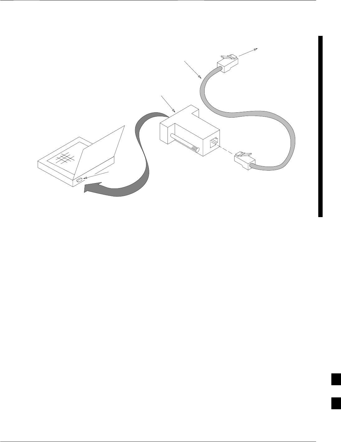
Terminal Setup – continued
FEB 2005 1X SC 4812T Lite BTS Optimization/ATP I-7
PRELIMINARY
To BTS
Router
CONSOLE
receptacle
COM1
OR
COM2
LMF COMPUTER
OR EQUIVALENT
OPTOATP0001–0
ROLLOVER
CABLE
DB9–TO–RJ48C
ADAPTER
Figure I-3: LMF Computer Connections to BTS Router
I

Downloading Minimum Canned BTS Router Configuration Files
I-8 1X SC 4812T Lite BTS Optimization/ATP FEB 2005
PRELIMINARY
Downloading Overview
After they are generated on the OMC–R, the BTS Router Canned
Configuration Files must be transferred to another computer platform
from which they can be installed into the BTS Routers. A number of
procedures may be used to move the Canned Configuration Files from
the OMC–R to a platform from which they can be loaded into the BTS
Routers. Some alternatives are:
1. If a Floppy Diskette drive is available at the OMC–R, such as the
one for UNO Workstations, the Configuration Files can be
transferred to an LMF Computer or similar machine using the CDF
File Transfer Procedure in the Preparing the LMF section of this
manual. Directories identified in Table I-3 must be used rather than
those in the CDF File Transfer Procedure.
2. If a Windows–based Server Connection is available in the operator’s
network and it can provide an FTP or Telnet Connection to the
OMC–R, files may be transferred by either the FTP or Telnet
methods.
3. If a Dial–up Connection is available for accessing the OMC–R, an
FTP or Telnet Session may be possible to transfer files to the
computer used to load the CF Memory Cards.
The procedure provided in this section covers FTP Transfer using a
Windows–based Server in the operator’s network. Coordinate with the
Local Network Administrator to determine the method and procedure to
use on a specific network.
Prerequisites
The following must be obtained from the Local Network Administrator
before performing the Canned Configuration File FTP Procedure in
Table I-3:
SUser ID and Password to log onto the OMC–R
SName of the subdirectory where the specific BTS Router Group
Canned Configuration Files to be downloaded were created.
FTP File Transfer from the
OMC–R
This procedure uses the Windows–based LMF Computer Platform to
download BTS Router Canned Configuration Files from the OMC–R.
Perform the procedure in Table I-3.
Table I-3: BTS Router Canned Configuration File FTP Transfer from the OMC–R
nStep Action
1If it has not been done, create a directory on the LMF Computer where the BTS Router Canned
Configuration Files will be stored.
2If it has not been done, obtain the OMC–R Logon User ID and Password from the Local Network
Administrator.
table continued on next page
I

Downloading Minimum Canned BTS Router Configuration Files – continued
FEB 2005 1X SC 4812T Lite BTS Optimization/ATP I-9
PRELIMINARY
Table I-3: BTS Router Canned Configuration File FTP Transfer from the OMC–R
nActionStep
3Connect the LMF Computer to the local network and log on.
NOTE
This procedure uses the Command Line FTP Client supplied with Windows 98, Second Edition
(Win98 SE) and Windows 2000 (Win2K); however, any commercially available FTP Client
Application can be used.
– Follow the manufacturer’s instructions for operation of an alternative application.
4Open a Command Line (MS DOS) Window by clicking on Start > Programs > Command
Prompt.
5When the Command Line Window opens, change to the directory where the Canned
Configuration Files will be stored on the LMF Computer by entering:
cd pathname
– Where pathname = the path to the required directory.
– A response similar to the following will be displayed:
C:\> cd Can_Cfg
C:\Can_Cfg>
6Check the contents of the directory by entering the following command.
dir
– A response similar to the following will be displayed:
C:\Can_Cfg>dir
Volume in drive C is MAIN
Volume Serial Number is F2AA–1721
Directory of C:\Can_Cfg>
08/22/2002 03:46p <DIR> .
08/22/2002 03:46p <DIR> ..
08/22/2002 03:46p 2,223 btsrtr_canned.blue
08/22/2002 03:47p 2,223 btsrtr_canned.red
2 File(s) 4,644 bytes
2 Dir(s) 2,556,045,312 bytes free
C:\Can_Cfg>
7If either or both of the following files are found in the directory, delete them or move them to
another directory:
–btsrtr_config.blue
–btsrtr_config.red
table continued on next page I

Downloading Minimum Canned BTS Router Configuration Files – continued
I-10 1X SC 4812T Lite BTS Optimization/ATP FEB 2005
PRELIMINARY
Table I-3: BTS Router Canned Configuration File FTP Transfer from the OMC–R
nActionStep
8Begin the FTP Session by entering the following command.
FTP hostname
– Where hostname = the OMC–R hostname or IP Address.
– A response similar to the following will be displayed:
C:\Can_Cfg> FTP OMC–R–1
C:\Can_Cfg>
Connected to OMC–R–1.
220 OMC–R–1 FTP Server (SunOS 5.6) ready.
User (OMC–R–1:(none)):
9Enter the User ID and Password when prompted, pressing the Enter Key after each.
– A response similar to the following will be displayed:
User (OMC–R–1:(none)): scadm
331 Password required for scadm.
Password:
230 User scadm logged in.
FTP>
10 Change to the directory where the BTS Router Canned Configuration File Subdirectories are
created.
11 Verify that the present Working Directory by entering the following commands, pressing the
Enter Key after each:
cd /home/scadm/btsrtr_canned_configs
pwd
– A response similar to the following will be displayed:
FTP> cd /home/scadm/btsrtr_canned_configs
240 CWD command successful.
FTP> pwd
245 ”/home/scadm/btsrtr_canned_configs” is current directory.
table continued on next page
I

Downloading Minimum Canned BTS Router Configuration Files – continued
FEB 2005 1X SC 4812T Lite BTS Optimization/ATP I-11
PRELIMINARY
Table I-3: BTS Router Canned Configuration File FTP Transfer from the OMC–R
nActionStep
12 Enter the ls Command to list the contents of the directory and ensure that the specific Canned
Configuration Directory Name provided by the administrator exists.
– A response similar to the following will be displayed:
FTP> ls
200 PORT command successful.
150 ASCII data connection for /bin/ls (10.182.29.117,80) (0 bytes).
Mon_Jul_2_01:55:07_CDT_2002
Wed_Jul_24_09:35:41_CDT_2002
Tue_Aug_04_10:35:22_CDT_2002
226 ASCII Transfer complete.
FTP: 30 bytes received in 0.02Seconds 1.50Kbytes/sec.
FTP>
NOTE
Directory Names where Canned Configuration Files are located will consist of the
weekday_month_day_time_year when the Canned Configuration Files were created on the
OMC–R.
13 Change to the directory specified for the BTS Router Group to be configured and list the directory
contents by entering the following, pressing the Enter Key after each command:
cd weekday_month_day_time_year
ls
– A response similar to the following will be displayed:
FTP> cd Wed_Jul_24_09:35:41_CDT_2002
250 CWD command successful.
FTP> ls
200 PORT command successful.
150 ASCII data connection for /bin/ls (10.182.29.117,80) (0 bytes).
btsrtr_canned.blue
btsrtr_canned.red
226 ASCII Transfer complete.
FTP: 39 bytes received in 0.05Seconds 0.78Kbytes/sec.
FTP>
table continued on next page
I

Downloading Minimum Canned BTS Router Configuration Files – continued
I-12 1X SC 4812T Lite BTS Optimization/ATP FEB 2005
PRELIMINARY
Table I-3: BTS Router Canned Configuration File FTP Transfer from the OMC–R
nActionStep
14 Change to the Binary Transfer Mode and, if desired, turn on Hash Mark Printing for transfer
progress by entering the following, pressing the Enter Key after each command:
bin
hash
– A response similar to the following will be displayed:
FTP> bin
200 Type set to I.
FTP> hash
Hash mark printing On FTP: (2048 bytes/hash mark).
FTP>
NOTE
With Win98 SE, turning on Hash Mark Printing can slow down File Transfer in certain
circumstances, but the Canned Configuration Files are quite small (approximately 2.5 KB) so
there should be little noticeable effect.
15 Download the BTS Router Canned Configuration Files to the LMF Computer by performing the
following actions.
15a Enter the following to download the first Canned Configuration File:
get btsrtr_canned.blue
– A response similar to the following will be displayed:
FTP> get btsrtr_canned.blue
200 PORT command successful.
150 Binary data connection for btsrtr_canned.blue (10.182.29.117,80) (2223 bytes).
#
226 Binary Transfer complete.
FTP: 2223 bytes received in 0.59Seconds 3.76Kbytes/sec.
FTP>
15b Enter the following to download the second BTS Router Canned Configuration File:
get btsrtr_canned.red
– A response similar to the following will be displayed:
FTP> get btsrtr_canned.red
200 PORT command successful.
150 Binary data connection for btsrtr_canned.red (10.182.29.117,80) (2223 bytes).
#
226 Binary Transfer complete.
FTP: 2223 bytes received in 0.59Seconds 3.76Kbytes/sec.
FTP>
table continued on next page
I

Downloading Minimum Canned BTS Router Configuration Files – continued
FEB 2005 1X SC 4812T Lite BTS Optimization/ATP I-13
PRELIMINARY
Table I-3: BTS Router Canned Configuration File FTP Transfer from the OMC–R
nActionStep
16 Before terminating the FTP Session, open Windows Explorer and view the contents of the
directory where the Canned Configuration Files are to be stored to ensure that the files are present.
Perform the following actions.
16a Click Start > Programs > Windows Explorer.
16b In the left–hand pane of Windows Explorer, perform one of the following depending on the LMF
Computer Operating System:
–Win98 SE: If necessary, expand the Directory Display for the drive where the Canned
Configuration File Storage Directory is located by clicking on the + next to the Drive Icon.
–Win2K: Expand the User Profile and Directory Display for the drive where the Canned
Configuration File Storage Directory is located by clicking on the + next to each icon,
respectively.
16c Expand any subdirectories as required to display the directory folder where the Canned
Configuration Files are to be stored.
16d Click on the Directory Folder Icon where the Canned Configuration Files are to be stored.
16e In the right–hand pane, verify that the files btsrtr_canned.blue and btsrtr_canned.red
appear.
16f If the files appear, proceed to Step 17.
16g If the files do not appear, repeat Step 15, its substeps, Step 16, and its substeps.
17 Close Windows Explorer.
18 In the Command Line Window, enter the bye Command to terminate the FTP Session.
– A response similar to the following will be displayed:
FTP> bye
221 Goodbye.
C:\Can_Cfg>
19 Close the Command Line Window by entering the exit Command.
20 BTS Router Canned Configuration Files are now ready for transfer to a BTS Router.
I

Verifying IOS Canned Version of the CF Memory Card
I-14 1X SC 4812T Lite BTS Optimization/ATP FEB 2005
PRELIMINARY
Overview
This section covers the procedures and commands required to verify that
the IOS Version loaded on BTS Router CF Memory Cards and copy
standard Canned Configuration Files to the BTS Routers. Because of the
set–up required and the length of some of the procedures, Motorola
recommends performing the actions covered in this section at a central
location to prepare the BTS Routers for installation prior to the site visit.
IOS Version Verification and
File Sequence Position
Version Verification
The IOS Version loaded on the BTS Router CF Memory Card should be
verified as the version required for operation on the network where the
BTS Routers will be installed. If the loaded IOS Version is not correct, it
can be replaced with a different version.
There are several methods available to accomplish Version Verification.
These depend on the equipment and Software Applications the user
selects to use in installing the Canned Configuration Files in the BTS
Routers. Appropriate Verification Procedures are included in each of the
two Canned Configuration Installation Methods covered in this section.
Methods to change the loaded IOS Version are provided in the Change
BTS Router IOS Version section of this appendix and are referenced at
the appropriate places in the Canned Configuration Installation
Methods..
File Sequence Position
During Initialization, the MWR 1941 Router will first search the
startup–config File for a Boot System Command Line telling it in
what directory and file to find the Boot Loader. If this line is not found,
the BTS Router will default to attempting to boot from the first file in its
Flash Memory.
Flash Memory for the MWR 1941 is the CF Memory Card (Software
Identifier slot0:). The Canned Configuration Files used for BTS Router
installation do not contain a Boot System Command Line because of the
need to maintain flexibility for IOS Version changes. Because of this, it
is critical that the IOS File is the first file listed on the CF Memory Card.
The Canned Configuration Installation Procedures contain Steps to
assure that this is the case, and, if it is not, provide guidance to correct
the condition. It is important to remember that, if the BTS Router boots
and displays a rommon 1 > Prompt, the IOS File is missing, out of
sequence, has a corrupted Flash Memory Image, or the
startup–config File contains a Boot System Line that specifies a
missing or incorrect IOS Pathname/Filename..
I

Verifying IOS Canned Version of the CF Memory Card – continued
FEB 2005 1X SC 4812T Lite BTS Optimization/ATP I-15
PRELIMINARY
Canned Configuration File
Installation
Filename and Installation Location Requirements
The Canned Configuration Files for the BTS Routers must be copied to
the CF Memory Card. The filename of the file on the CF Memory Card
must be canned–config.
Canned Configuration File Location and Filename Requirements are a
result of Mobile Wireless Center (MWC) Actions during the process of
switching a BTS from Packet to Circuit Mode. In this process, the MWC
will query the BTS Routers’ slot0: Directory for a file named
canned–config. A missing or misnamed file will cause problems with
execution of the Mode–switching Process..
Installation Methods
The startup–config Configuration File used by the BTS Router
during Initialization is stored in NVRAM. This is a memory device
internal to the BTS Router and is separate from the CF Memory Card.
To install the Canned Configuration File so the BTS Router will use it
during Boot–up, the file must be copied into the startup–config File
in NVRAM.
There are two methods available to accomplish this.:
1. Using a TFTP Server Application to copy the Canned Configuration
File from the Windows–based LMF Computer to the CF Memory
Card installed in a BTS Router, and then copying it to the
startup–config File in the BTS Router’s NVRAM.
2. Using a CF Memory Card Reader to copy the Canned Configuration
File to a CF Memory Card, and then, once the CF Memory Card is
installed in the BTS Router, using a HyperTerminal Communication
Session to copy the file from the CF Memory Card to the
startup–config File in the BTS Router’s NVRAM.
Comparison of Methods
Preparation for using the TFTP Server Application Method is extensive
and requires setting up simultaneous Serial and FE Communication
Sessions with the BTS Router. This method offers the advantage of
being able to verify IOS File Sequence Position immediately, and
supporting Direct File Transfers between the BTS Router and LMF
Computer without removing the CF Memory Card.
As an alternative, using a CF Memory Card Reader to copy the Canned
Configuration File to a CF Memory Card, and from there to the
startup–config File requires very little set–up. With this method, the
IOS File Sequence Position can only be verified once the CF Memory
Card is installed in the BTS Router, and any file transfers between the
BTS Router and LMF Computer require physically moving the CF
Memory Card between the BTS Router and Card Reader..
I

Verifying IOS Canned Version of the CF Memory Card – continued
I-16 1X SC 4812T Lite BTS Optimization/ATP FEB 2005
PRELIMINARY
Procedures to use Each Method
Using the TFTP Server Application to copy the Canned Configuration
File to a CF Memory Card is covered in the Method 1 subsection.
Performing the Transfer Process with a Card Reader is covered in the
Method 2 subsection. The applicable procedures for verifying the loaded
IOS Version and File Sequence Position are included in each method..
File Operations using a CF Memory Card Reader
File Transfers should only be performed using the CF Memory Card
Reader. CF Memory Card Formatting should be performed in a BTS
Router using a HyperTerminal Connection. Attempting to format a CF
Memory Card from a Windows–based computer using a Card Reader
could result in unpredictable BTS Router Operation..
Do not format BTS Router CF Memory Cards using a
Windows–based computer. Format CF Memory Cards only
in a BTS Router.
CAUTION
Method 1: Using a TFTP Server
to Load to CF Memory Card
Required Equipment and Software
The following items are required to perform this procedure:
SA Windows–based computer that meets the requirements of the LMF
Computer Platform as specified in this manual.
SOne of the following Operating Systems for the Windows–based
computer:
–Windows 2000
–Windows 98 Second Edition (SE) using the FAT32 File System
BTS Router CF Memory Cards loaded using computers
equipped with Windows 98 Versions earlier than Windows
98 SE and using the FAT16 File System will not operate
properly, resulting in a complete site outage.
CAUTION
SOne of the following for the Windows–based computer:
– Internal 10/100baseT Network Interface Card (NIC)
– PCMCIA 10/100baseT NIC
I

Verifying IOS Canned Version of the CF Memory Card – continued
FEB 2005 1X SC 4812T Lite BTS Optimization/ATP I-17
PRELIMINARY
SCable, Ethernet Crossover, Category 5E or better, unshielded twisted
pair, two 8–contact Modular Plugs, in one of the following lengths, as
determined necessary:
– 0.3 m (11.8 in) (Motorola Part Number 3088643C07)
– 0.6 m (23.6 in) (Motorola Part Number 3088643C13)
– 1.0 m (39.4 in) (Motorola Part Number 3088643C15)
– 2.1 m (84 in) (Motorola Part Number 3088643C08)
– 3.0 m (120 in) (Motorola Part Number 3088643C09)
SCable, Rollover, as described in the Establishing a BTS Router
Communication Session section of this appendix
SDB–9 plug–to–8–contact Modular Plug Adapter as described in the
Establishing a BTS Router Communication Session section of this
appendix
SA TFTP Server Software Application (refer to the Setting Up the
TFTP Server – Procedure in Cellular System Administration – CDMA
OnLine Documentation) such as:
– Cisco TFTP Server
– PumpKIN TFTP Server
– Any other equivalent TFTP Server Application
SA copy of the MWR 1941 Router IOS Version required for the
network in which the BTS Routers are to be installed. (Contact the
Network Administrator or the Motorola Account Team for information
on obtaining the required MWR 1941 IOS Version.)
SA +27V DC Power Supply Module to power the BTS Router during
Configuration File Operations
Required Materials
The following material is required to perform this method:
SMarking material to identify the BTS Router and CF Memory Card
with the installed configuration (blue or red)
Required Publications
The following publications are required to perform procedures in this
section:
Sthis manual: 1X SC4812T Lite BTS Optimization/ATP manual
(68P09262A58)
SCellular System Administration – CDMA OnLine Documentation
SMWR1941 Wireless Mobile Edge Router Software Configuration
Guide; part number 78–13983–01 I
Verifying IOS Canned Version of the CF Memory Card – continued
I-18 1X SC 4812T Lite BTS Optimization/ATP FEB 2005
PRELIMINARY
Preparation for Canned Configuration File TFTP Transfer to
CF Memory Card
Preparation for a Canned Configuration File TFTP Transfer consists of
the following activities:
1. Setting the LMF Computer NIC IP Address
2. Creating a directory (folder) on the LMF Computer to be used for all
TFTP File Transfers
3. Installing the TFTP Server Application on the LMF Computer, and
setting the TFTP Server Application Root Directory to the directory
created in 2, above
4. Connecting the LMF Computer to the BTS Router for both
HyperTerminal (serial) and Ethernet Communication
5. BTS Router Power–up and Initial Configuration for Ethernet
Communication
The following procedures are used to accomplish all of these preparatory
actions.
Set LMF Computer NIC TCP/IP Address and Create the
Default TFTP Directory
Perform the procedure in Table I-4 to set the NIC IP Address..
If the IP Address for the LAN Connection on an LMF
Computer is being changed to support TFTP Downloads to
a BTS Router, the BTS 10base–2 LAN IP Address and
Subnet Mask for the NIC must be restored before the LMF
can log into a BTS to perform an Optimization or ATP.
IMPORTANT
*
There are differences between Windows 2000 and Windows
98 in the menus and screens used for setting or changing a
NIC Connection. In the following procedure, items
applicable to:Windows 2000 will be identified with
Win2000Windows 98 will be identified with Win98
NOTE
Table I-4: Set LMF Computer NIC IP Address and Create a Default TFTP Directory
nStep Action
1Start the computer.
2Login and allow the computer to boot to the Desktop.
table continued on next page
I

Verifying IOS Canned Version of the CF Memory Card – continued
FEB 2005 1X SC 4812T Lite BTS Optimization/ATP I-19
PRELIMINARY
Table I-4: Set LMF Computer NIC IP Address and Create a Default TFTP Directory
nActionStep
3Depending on the installed Operating System, from the Windows Start Menu, select one of the
following:
SWin2000: Settings > Network and Dial–up Connections
SWin98: Settings > Control Panel and double–click Network.
4Perform one of the following as applicable for the installed Operating System:
SFor Win2000, in the list of displayed connections, locate the Local Area Network Connection
for the NIC to be used for BTS Router Ethernet Communication.
SFor Win98, in the Configuration Tab of the Network Dialog Box, locate the TCP/IP
Connection for the installed NIC.
– If TCP/IP does not appear in the displayed list of installed network components, refer to the
Operating System Documentation and install TCP/IP.
5Perform one of the following as applicable for the installed Operating System:
SFor Win2000:
– Highlight the connection for the NIC.
– Right–click the highlighted connection.
– Select Properties from the Pop–up Menu.
SFor Win98:
– Highlight the TCP/IP NIC Connection in the displayed list of installed network components.
– Click the Properties Button.
– Skip to Step 8.
6 For Win2000 , in the Local Area Connection Properties Dialog Box that appears:
Sif Internet Protocol (TCP/IP) is showing in the Components checked are used by this
connection: List Box, proceed to Step 7.
Sif Internet Protocol (TCP/IP) is not showing in the Components checked are used by this
connection: List Box, refer to the Operating System Documentation and install TCP/IP.
7 For Win2000, if the Check Box next to the Internet Protocol (TCP/IP) Entry is not checked, click
in the box to check it.
8Perform one of the following:
SWin2000:
– Highlight the Internet Protocol (TCP/IP) Entry.
– Click on the Properties Button below the Components checked are used by this
connection: List Box.
SWin98:
– From the Tabs displayed in the TCP/IP Properties Dialog Box that opens, select the IP
Address Tab if it is not at the front.
table continued on next page
I

Verifying IOS Canned Version of the CF Memory Card – continued
I-20 1X SC 4812T Lite BTS Optimization/ATP FEB 2005
PRELIMINARY
Table I-4: Set LMF Computer NIC IP Address and Create a Default TFTP Directory
nActionStep
9In the Internet Protocol (TCP/IP) Properties Dialog Box that appears (Win2000) or the IP
Address Tab of the TCP/IP Properties Dialog Box (Win98), perform the following actions.
9a If a black dot is not showing in the the Radio Button Circle next to Use the following IP
Address: (Win2000) or Specify an IP Address (Win98), click on the Radio Button.
– A black dot will appear in the circle.
9b If using an LMF Computer, record the IP Address and Subnet Mask used for LMF–BTS
Communication so they can be re–entered when TFTP Transfer Activities for the BTS Router are
completed.
9c Enter 100.100.100.1 in the IP Address: Box.
9d Enter 255.255.255.252 in the Subnet Mask: Box.
10 Click the OK Button for the Internet Protocol (TCP/IP) Properties Dialog Box (Win2000) or
the TCP/IP Properties Box (Win98).
11 Click the OK Button for the Local Area Connection Properties Box (Win2000) or the Network
Box (Win98).
12 In Win98, click File > Close to close the Control Panel Window.
13 Click Start > Programs > Windows Explorer to open Windows Explorer.
14 If the Default TFTP Directory is to be the same directory in which the files downloaded from the
OMC–R are stored, proceed to Step 22.
15 In the left–hand pane of Windows Explorer, locate the icon for the drive where the Default TFTP
Directory is to be created.
16 Highlight the Drive Icon and click Files > New > Folder.
17 While observing the new folder icon in the right–hand pane, type the name for the folder (for
example, TFTP_files), and press the Enter Key.
18 In Windows Explorer, locate the directory where the Canned Configuration Files that were
downloaded from the OMC–R are stored.
19 In the left–hand pane, highlight the directory where the files are stored.
20 Scroll the left–hand pane until the newly–created Default TFTP Directory is visible.
21 In the right–hand pane, highlight the Canned Configuration Files and drag them to the Default
TFTP Directory.
22 In the left–hand pane, click on the Default TFTP Directory, and verify that the Canned
Configuration Files appear in the right–hand pane.
23 Load a copy of the required BTS Router IOS Version into the Default TFTP Directory using FTP,
Internet Download, or media such as a Zip Disk (file size is over 7 MB).
24 Click Files > Close to close Windows Explorer.
I
Verifying IOS Canned Version of the CF Memory Card – continued
FEB 2005 1X SC 4812T Lite BTS Optimization/ATP I-21
PRELIMINARY
Install and Configure TFTP Server Application
To obtain, install, and configure the Cisco or PumpKIN TFTP Software
Applications, refer to the Setting Up the TFTP Server – Procedure in
Cellular System Administration – CDMA OnLine Documentation For
other TFTP Server Applications, install and configure the application
according to the manufacturer’s instructions..
When entering the name of the TFTP Server Root
Directory while configuring the TFTP Server Application,
be sure to use the name of the directory identified in
Table I-4, Step 14, or created in Table I-4, Step 17, above.
IMPORTANT
*
Connect the LMF Computer to the BTS Router
Connect the LMF Computer to the BTS Router by performing the
procedure in Table I-5 and referring to Figure I-4..
Table I-5: Connecting the LMF Computer to the BTS Router for TFTP File Transfer
nStep Action
1If the BTS Router has not been connected to a Power Source, perform the following actions.
1a Ensure that the +27V DC Power Source is not ON.
1b Connect the BTS Router to the +27V DC Power Source.
2Connect the LMF Computer to the BTS Router as shown in Figure I-4, referring to the list of
required equipment in this section as required.
3If the LMF Computer has not been started, turn it on, Login, and allow it to boot to the Desktop.
4Start a HyperTerminal Communication Session for the BTS Router.
– Refer to the procedure in Table I-2 of this appendix.
5Start the TFTP Server Application as specified for the software.
– Refer to the Setting Up the TFTP Server – Procedure in Cellular System Administration –
CDMA OnLine Documentation or the manufacturer’s instructions.
I
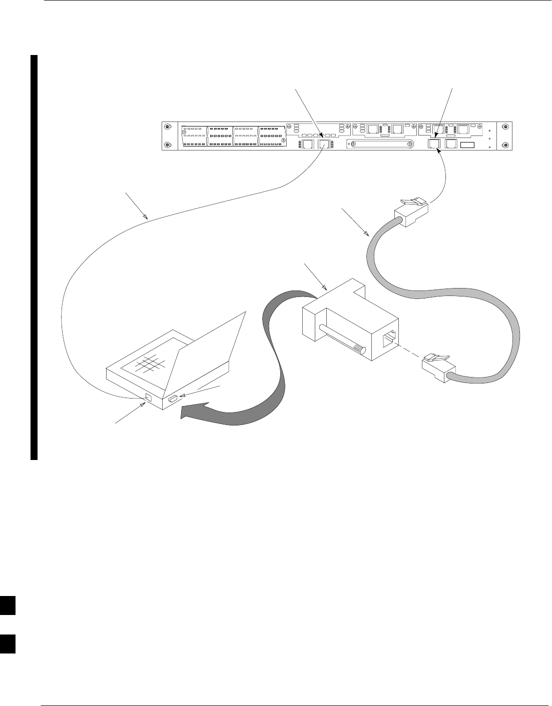
Verifying IOS Canned Version of the CF Memory Card – continued
I-22 1X SC 4812T Lite BTS Optimization/ATP FEB 2005
PRELIMINARY
To BTS
Router
CONSOLE
receptacle
COM1
OR
COM2
LMF COMPUTER
OR EQUIVALENT
ROLLOVER
CABLE
DB9–TO–RJ48C
ADAPTER
BTSRTR0025
ETHERNET
CROSSOVER
CABLE
10/100BASE T
NIC PORT
FAST ETHERNET PORT FE 0
(SOFTWARE DESIGNATION FA0/0) CONSOLE
PORT
Figure I-4: LMF Computer TFTP Connections to BTS Router
I

Verifying IOS Canned Version of the CF Memory Card – continued
FEB 2005 1X SC 4812T Lite BTS Optimization/ATP I-23
PRELIMINARY
BTS Router Power–up and Initial Configuration for Ethernet
Communication
Perform the procedure in Table I-6 to apply power to the BTS Router
and set an Initial Configuration for Ethernet Communication.
SEnsure that the required version of the IOS is loaded on the CF
Memory Card.
SEnsure that the CF Memory Card is installed in the BTS Router.
Table I-6: BTS Router Power–up and Initial Ethernet Configuration Procedure
nStep Action
* IMPORTANT
This procedure does not cover all aspects of BTS Router Operation and programming.
Before performing this procedure, review BTS Router initialization, operation, and programming
information and procedures in MWR1941 Wireless Mobile Edge Router Software Configuration
Guide; part number 78–13983–01.
– Have this publication available for reference while performing this procedure.
1Ensure that a CF Memory Card loaded with the Cisco IOS is installed in the BTS Router.
– Refer to the BTS Router Card and Module Replacement section of the 1X SC4812T Lite BTS
FRU manual (68P09262A60) for instructions to access the CF Memory Card Slot.
* IMPORTANT
In Step 2, do not touch the computer keyboard until the BTS Router completes the Boot Process.
The BTS Router buffers any keystrokes made during the Boot Process and interprets them as
commands to be executed immediately following completion of the Boot Process.
2Apply power to the BTS Router and allow it to complete the Boot Process.
SIf a message similar to the following, is displayed, press the Enter Key and proceed to Step 3.
Press RETURN to get started!
SIf a message similar to the following, is displayed type no and press the Enter Key:
Basic management set–up configures only enough connectivity
for management of the system, extended set–up will ask you
to configure each interface on the system
Would you like to enter basic management set–up? [yes/no]:
A response similar to the following will be displayed:
Would you like to enter basic management set–up? [yes/no]: no
Cisco Internetwork Operating System Software
IOS (tm) 1941 Software (MWR1941–I–M), Version 12.2(20020127:101239
Copyright (c) 1986–2002 by cisco Systems, Inc.
Compiled Sun 27–Jan–02 06:08 by walrobin
Router>
table continued on next page
I

Verifying IOS Canned Version of the CF Memory Card – continued
I-24 1X SC 4812T Lite BTS Optimization/ATP FEB 2005
PRELIMINARY
Table I-6: BTS Router Power–up and Initial Ethernet Configuration Procedure
nActionStep
3At the Router> User EXEC Mode Prompt, enter the following to access the Privileged EXEC
Mode:
enable
– A response similar to the following will be displayed:
Router>enable
Router#
4At the Router# Privileged EXEC Mode Prompt, enter the following to access the Configure
Submode:
configure terminal
– A response similar to the following will be displayed:
Router#conf t
Enter configuration commands, one per line. End with CNTL/Z.
Router(config)#
– The BTS Router is now in the Global Configuration Mode and ready to accept configuration
changes entered from the keyboard.
5At the Global Configuration Mode Prompt, type each of the following commands, pressing the
Enter Key after each command:
hostname btsrtr1
interface fa0/0
ip address 100.100.100.2 255.255.255.252
speed 100
duplex full
no shutdown
line con 0
exec–timeout 0 0
no Login
line vty 0 4
no Login
– Responses similar to the following will be displayed:
Router(config)#hostname BTSRTR1
BTSRTR1(config)#interface fa0/0
BTSRTR1(config–if)#ip address 100.100.100.2 255.255.255.252
BTSRTR1(config–if)#speed 100
BTSRTR1(config–if)#duplex full
BTSRTR1(config–if)#no shutdown
BTSRTR1(config–if)#line con 0
BTSRTR1(config–line)#exec–timeout 0 0
BTSRTR1(config–line)#no Login
BTSRTR1(config–line)#line vty 0 4
BTSRTR1(config–line)#no Login
BTSRTR1(config–line)#
table continued on next page
I

Verifying IOS Canned Version of the CF Memory Card – continued
FEB 2005 1X SC 4812T Lite BTS Optimization/ATP I-25
PRELIMINARY
Table I-6: BTS Router Power–up and Initial Ethernet Configuration Procedure
nActionStep
6Once the correct parameters have been set, return to the Privileged EXEC Mode Prompt by
holding down the Ctrl Key and pressing z (Ctrl+z).
– A response similar to the following will be displayed.
BTSRTR1(config–line)# ^z
01:11:27: %SYS–5–CONFIG_I: Configured from console by console
BTSRTR1#
NOTE
Entering exit twice and pressing the Enter Key after each entry, will also complete the
Configuration Process and return the BTS Router to the Privileged EXEC Mode.
7Verify that Port FE 0 (fa0/0) is configured with the correct IP Address by entering the following
command.
show ip interface brief
– A response similar to the following will be displayed.
BTSRTR1#sh ip int br
Interface IP Address OK? Method Status Protocol
FastEthernet0/0 100.100.100.2 YES manual up up
Serial0:0 unassigned YES unset administratively down down
FastEthernet0/1 unassigned YES unset administratively down down
Serial1:0 unassigned YES unset administratively down down
BTSRTR1#
8The BTS Router is now configured for Ethernet Communication on FE 0, and the Canned
Configuration File can be transferred by TFTP.
– Proceed to Table I-7.
Verifying IOS Version and Canned Configuration File TFTP
Transfer to the BTS Router
Prerequisites – The following is required prior to performing this
procedure.:
SA copy of the required MWR 1941 Router IOS Version file is
installed in the Default TFTP Directory. Transfer the file to the LMF
Computer using FTP, Internet Download, or media such as a Zip Disk;
file size is approximately 7–8 MB.
IOS Verification and Canned Configuration File Transfer – Perform
the procedure in Table I-7 to verify that the loaded IOS Version and
transfer the Canned Configuration Files from the LMF Computer to the
BTS Router CF Memory Card..
I

Verifying IOS Canned Version of the CF Memory Card – continued
I-26 1X SC 4812T Lite BTS Optimization/ATP FEB 2005
PRELIMINARY
MWR 1941 Routers must be loaded with IOS Version
mwr1900–i–mz.122–8.MC2d.bin or later. This Router
model will not function properly with earlier IOS Versions.
IMPORTANT
*
This procedure does not cover all aspects of BTS Router
Operation and programming.
Before performing this procedure, review BTS Router
initialization, operation, and programming information
and procedures in MWR1941 Wireless Mobile Edge
Router Software Configuration Guide; part number
78–13983–01.
Have this publication available for reference while
performing this procedure.
NOTE
Table I-7: Transfer Canned Configuration Files to the BTS Router Using a TFTP Server
nStep Action
! CAUTION
If Personal Firewall and/or Intrusion Detection Software such as Black ICE is running on the LMF
Computer, shut it down before performing this procedure.
– If this is not done, the TFTP Transfer Process will not operate.
1On the LMF Computer, if it has not been done, start the TFTP Server according to the
manufacturer’s directions.
– Refer to the Setting Up the TFTP Server – Procedure in the Cellular System Administration –
CDMA OnLine Documentation.
* IMPORTANT
MWR 1941 Routers must be loaded with IOS Version mwr1900–i–mz.122–8.MC2d.bin or later.
– This Router model will not function properly with earlier IOS Versions.
2If a HyperTerminal Communication Session with the BTS Router is not running, start one by
performing the procedure in Table I-2.
3In the HyperTerminal Window, the BTS Router must be in the Privileged EXEC Mode, as
indicated by a number sign at the end of the prompt:
BTSRTR1#
4Ensure that the Ethernet Crossover Cable is connected between the LMF Computer NIC Port and
the BTS Router FE 0 Port.
– Refer to Figure I-4.
table continued on next page
I

Verifying IOS Canned Version of the CF Memory Card – continued
FEB 2005 1X SC 4812T Lite BTS Optimization/ATP I-27
PRELIMINARY
Table I-7: Transfer Canned Configuration Files to the BTS Router Using a TFTP Server
nActionStep
5Begin verification that the CF Memory Card contains the correct version of the Cisco IOS by
entering the following command.
dir slot0:
– A response similar to the following will be displayed:
BTSRTR1#dir slot0:
Directory of slot0:/
1 –rw– 7051976 Mar 01 1993 00:11:34 mwr1941–i–mz.122–8.MC2a.bin
31932416 bytes total (24879104 bytes free)
BTSRTR1#
6Identify the present Working Directory by entering pwd.
– The IOS defaults to the CF Memory Card (slot0:) Directory unless the present Working
Directory has been changed by using the cd Command.
7If the present Working Directory has been changed, enter the command cd slot0: to return to
the default setting.
– If slot0: is included in the command, be sure to include the colon (:) after slot0 when typing
the command.
– The IOS Filename will be similar to the following example.
mwr1941–i–mz.122–8.MC2a.bin
table continued on next page
I

Verifying IOS Canned Version of the CF Memory Card – continued
I-28 1X SC 4812T Lite BTS Optimization/ATP FEB 2005
PRELIMINARY
Table I-7: Transfer Canned Configuration Files to the BTS Router Using a TFTP Server
nActionStep
8Direct the BTS Router to show the Version Information by entering the following command.
show version
– A response similar to the following will be displayed:
BTSRTR1#sh ver
Cisco Internetwork Operating System Software
IOS (tm) 1941 Software (MWR1941–I–M), Version 12.2(8)MC2a, EARLY DEPLOYMENT RE-
LEASE SOFTWARE (fc1)
TAC Support: http://www.cisco.com/tac
Copyright (c) 1986–2002 by cisco Systems, Inc.
Compiled Mon 05–Aug–02 11:07 by nmasa
Image text–base: 0x60008940, data–base: 0x60B54000
ROM: System Bootstrap, Version 12.2(20020113:235343) [sbose–wilma 109], DEVELOP-
MENT SOFTWARE
ROM: 1941 Software (MWR1941–I–M), Version 12.2(8)MC2a, EARLY DEPLOYMENT RELEASE
SOFTWARE (fc1)
Router uptime is 1 minute
System returned to ROM by power–on
System image file is ”slot0:mwr1941–i–mz.122–8.MC2a.bin”
cisco mwr1941 (R7000) processor (revision 0.1) with 121856K/18432K bytes of
memory.
Processor board ID JMX0611K5TS
R7000 CPU at 240Mhz, Implementation 39, Rev 3.3, 256KB L2 Cache
Bridging software.
X.25 software, Version 3.0.0.
Primary Rate ISDN software, Version 1.1.
Toaster processor tmc is running.
2 FastEthernet/IEEE 802.3 interface(s)
2 Serial network interface(s)
2 Channelized T1/PRI port(s)
DRAM configuration is 64 bits wide with parity disabled.
55K bytes of non–volatile configuration memory.
31360K bytes of ATA Slot0 CompactFlash (Read/Write)
Configuration register is 0x101
BTSRTR1#
9Compare the IOS Filename returned in Step 5 and the second line of the Version Information in
Step 8.
– Note the correspondence between the filename and IOS Version information.
SIf the IOS Filename from the CF Memory Card returned in Step 5 is not different than the
filename of the required IOS Version loaded in the LMF Computer Default TFTP Directory,
proceed to Step 11.
SIf the IOS Filename from the CF Memory Card returned in Step 5 is different than the filename
of the required IOS Version loaded in the LMF Computer Default TFTP Directory, proceed to
Step 10.
10 Perform the procedure in Table I-13 to load the required version, then proceed to Step 11.
table continued on next page
I

Verifying IOS Canned Version of the CF Memory Card – continued
FEB 2005 1X SC 4812T Lite BTS Optimization/ATP I-29
PRELIMINARY
Table I-7: Transfer Canned Configuration Files to the BTS Router Using a TFTP Server
nActionStep
! CAUTION
The File Sequence on the CF Memory Card can not be verified with Application Programs that
place the listed file names in alphabetical order (for example, certain UNIX Telnet Applications,
UNIX Directory Listing Commands, and Windows File Managers such as Windows Explorer).
This portion of the procedure is intended for use only with applications, such as HyperTerminal,
that do not list directory contents alphabetically.
11 Verify that the IOS Version is correct.
SIf the IOS Version is correct and there is more than one file loaded on the CF Memory Card,
ensure that the IOS File is the first file listed in the Directory Content Display.
SIf it is not correct, proceed to Step 12.
12 Prepare the LMF for the correct IOS Version.
12a Backup all files on the CF Memory Card to the LMF Computer Default TFTP Directory by
performing Step 3 through Step 6 of Table I-13.
12b Perform Step 25 through Step 30 of Table I-13, as applicable.
12c Type the following to delete a possible Boot System Line in the startup–config File, pressing
the Enter Key after the command and at each prompt to confirm the filename and deletion
operation.
del nvram:startup–config
– A response similar to the following will be displayed:
BTSRTR1#del nvram:startup–config
Delete filename [startup–config]?
Delete nvram:startup–config? [confirm]
[OK]
BTSRTR1#
NOTE
Ensure to include the colon (:) after nvram when typing the command.
12d Verify that the startup–config File size has been reduced to a minimum by entering the
following command.
dir nvram:
– A response similar to the following will be displayed:
Router#dir nvram:
Directory of nvram:/
53 –rw– 5 <no date> startup–config
54 –––– 5 <no date> private–config
57336 bytes total (57274 bytes free)
BTSRTR1#
table continued on next page
I

Verifying IOS Canned Version of the CF Memory Card – continued
I-30 1X SC 4812T Lite BTS Optimization/ATP FEB 2005
PRELIMINARY
Table I-7: Transfer Canned Configuration Files to the BTS Router Using a TFTP Server
nActionStep
13 At the Privileged EXEC Mode Prompt, enter the following command.
copy TFTP:btsrtr_canned.color slot0:canned–config
– Where color = blue or red, as applicable.
– A response similar to the following will be displayed:
BTSRTR1#copy TFTP:btsrtr_canned.blue slot0:canned–config
Address or name of remote host []?
14 At the prompt for the Remote Host Address or Name, enter the IP Address of the LMF Computer
NIC:
100.100.100.1
– A response similar to the following will be displayed:
BTSRTR1#copy TFTP:btsrtr_canned.blue slot0:canned–config
Address or name of remote host []? 100.100.100.1
Destination filename [canned–config]?
15 At the prompt for the Destination Filename, press the Enter Key.
– A response similar to the following will be displayed:
BTSRTR1#copy TFTP:btsrtr_canned.blue slot0:canned–config
Address or name of remote host []? 100.100.100.1
Destination filename [canned–config]?
Loading btsrtr_canned.blue from 100.100.100.1 (via Ethernet0/0): !
[OK – 2457/4096 bytes]
2457 bytes copied in 84.724 secs (29 bytes/sec)
BTSRTR1#
16 Verify that the Canned Configuration File is saved on the CF Memory Card by entering the dir
Command.
– A response similar to the following will be displayed:
Directory of slot0:/
1 –rw– 7051976 Mar 01 1993 00:11:34 mwr1941–i–mz.122–8.MC2a.bin
2 –rw– 2457 Mar 01 1993 00:14:48 canned–config
31932416 bytes total (24877983 bytes free)
BTSRTR1#
17 To allow the BTS Router to boot using the Canned Configuration, enter the following command.
copy canned–config startup–config
– A response similar to the following will be displayed:
BTSRTR1#copy canned–config start
Destination filename [startup–config]?
table continued on next page
I

Verifying IOS Canned Version of the CF Memory Card – continued
FEB 2005 1X SC 4812T Lite BTS Optimization/ATP I-31
PRELIMINARY
Table I-7: Transfer Canned Configuration Files to the BTS Router Using a TFTP Server
nActionStep
18 When prompted for the Destination File Name, press the Enter Key.
– A response similar to the following will be displayed:
BTSRTR1#copy canned–config start
Destination filename [startup–config]?
2457 bytes copied in 3.52 secs
BTSRTR1#
19 Display and note the file size of the startup–config File by entering the following command.
dir nvram:
– A response similar to the following will be displayed:
Directory of nvram:/
26 –rw– 2457 <no date> startup–config
27 –––– 5 <no date> private–config
29688 bytes total (24774 bytes free)
BTSRTR1#
20 Scroll the HyperTerminal Window back to the slot0: Directory Display obtained in Step 16,
above.
21 Compare the file size of the startup–config File to the Canned Configuration File to verify the
Copy Operation.
– The file sizes should be the same.
22 If desired, the contents of the startup–config File may be verified against the file listings at
the end of this appendix for the blue or red Canned Configuration, as applicable, by entering the
following command.
show startup–config
NOTE
Pressing the Space Bar at the MORE prompt will scroll another full screen of data.
Pressing the Enter Key will scroll the screen one line at a time.
23 Verify that the BTS Router will boot properly on the IOS and revised Start–up
Configuration Files by entering the following command.
reload
– A response similar to the following will be displayed:
BTSRTR1#reload
System configuration has been modified. Save? [yes/no]: n
Proceed with reload? [confirm]
24 If prompted to save a modified configuration, enter n for “no,” and press the Enter Key.
25 When prompted to proceed with Reload, press the Enter Key to continue the Reload Operation.
table continued on next page
I

Verifying IOS Canned Version of the CF Memory Card – continued
I-32 1X SC 4812T Lite BTS Optimization/ATP FEB 2005
PRELIMINARY
Table I-7: Transfer Canned Configuration Files to the BTS Router Using a TFTP Server
nActionStep
26 Verify that the BTS Router reboots without displaying the rommon 1 > Prompt or Error Messages
related to Port Configurations.
SIf the BTS Router boots to the ROMMON Prompt, proceed to the Recovery from BTS Router
Boot to ROMMON section of this appendix.
27 Using the tagging materials, tag the BTS Router to clearly identify the installed configuration
[blue (BTSRTR1) or red (BTSRTR2)].
28 Remove the CF Memory from the BTS Router by performing the procedure in the 1X SC4812T
Lite BTS FRU manual (68P09262A60) Manual.
29 Mark the installed configuration (blue or red) on the Card Label.
30 Install the card in the BTS Router by performing the procedure in the 1X SC4812T Lite BTS FRU
manual (68P09262A60)
31 If an additional BTS Router needs have the Canned Configuration installed, perform the following
actions.
31a Disconnect the cabling from the BTS Router.
31b Remove power from the BTS Router and disconnect it from the Power Supply Module.
31c Repeat the procedures in Table I-5, Table I-6, and this table (Table I-7) using the additional BTS
Router.
32 If no additional BTS Routers must be configured, perform Steps 31a and 31b, then proceed to
Step 33.
33 On the LMF Computer, shut down the TFTP Server Application and exit the HyperTerminal
Session.
34 If no additional TFTP Transfer activities are to be performed, change the NIC IP Address and
Subnet Mask back to those for LMF–BTS Communication recorded in Table I-4, Step 9b.
! CAUTION
If the BTS 10base–2 LAN IP Address and Subnet Mask for the LMF Computer’s NIC are not
restored, the LMF can not log into a BTS when attempting to perform a BTS Optimization or
ATP.
I
Verifying IOS Canned Version of the CF Memory Card – continued
FEB 2005 1X SC 4812T Lite BTS Optimization/ATP I-33
PRELIMINARY
Method 2: Using a CF Memory
Card Reader to Load CF
Memory Card
Required Equipment and Software
The following items are required to perform this procedure:
SA Windows–based computer that meets the requirements of the LMF
Computer Platform as specified in this manual.
SOne of the following Operating Systems for the Windows–based
computer:
–Windows 2000
–Windows 98 Second Edition (SE) using the FAT32 File System
BTS Router CF Memory Cards loaded using computers
equipped with Windows 98 Versions earlier than Windows
98 SE and using the FAT16 File System will not operate
properly, resulting in a complete site outage.
CAUTION
SCompact Flash Memory Card Reader Device and Software Driver for
the Operating System installed on the LMF Computer
Card Readers for other non–volatile, solid–state memory
devices such as Smart Media Cards will not work with the
CF Memory Cards used in the MWR 1941 Routers. Do not
attempt to use a Card Reader intended for another type of
memory device.
CAUTION
SCable, Rollover, as described in the Establishing a BTS Router
Communication Session section of this appendix
SDB–9 plug–to–8–contact Modular Plug Adapter as described in the
Establishing a BTS Router Communication Session section of this
appendix
SA copy of the MWR 1941 Router IOS Version required for the
network where the BTS Routers are to be installed (Contact the
Network Administrator and the Motorola Account Team for
information on obtaining the required MWR 1941 IOS Version.)
SA +27V DC Power Supply Module to power the BTS Router during
Configuration File Operations.
Required Materials
The following material is required to perform this method:
STagging and marking material to identify the BTS Router and CF
Memory Card with the installed configuration (blue or red).
I
Verifying IOS Canned Version of the CF Memory Card – continued
I-34 1X SC 4812T Lite BTS Optimization/ATP FEB 2005
PRELIMINARY
Required Publications
The following publications are required to perform procedures in this
section:
SCellular System Administration – CDMA OnLine Documentation
SMWR1941 Wireless Mobile Edge Router Software Configuration
Guide; part number 78–13983–01
File Operations Using a CF Memory Card Reader
Only File Transfers should be performed using the CF Memory Card
Reader. CF Memory Card Formatting should be performed in a BTS
Router using a HyperTerminal Connection. Attempting to format a CF
Memory Card from a Windows–based computer using a Card Reader
could result in unpredictable BTS Router Operation.
Do not format BTS Router CF Memory Cards using a
Windows–based computer. Only format CF Memory Cards
in a BTS Router.
CAUTION
Verifying IOS Version and Loading BTS Router Canned
Configuration File to CF Memory Card Using a CF Memory
Card Reader
The process of transferring a Canned Configuration File to a BTS Router
using a CF Memory Card Reader consists of the following activities:
1. Transfer the Canned Configuration File to the BTS Router’s CF
Memory Card using a CF Memory Card Reader.
2. Copy the file from the CF Memory Card to the BTS Router’s
startup–config File.
The following procedures are used to accomplish these actions.
Prerequisites
The following is required prior to performing this procedure.:
SA copy of the required MWR 1941 Router IOS Version file is
installed in the Default TFTP Directory (transfer the file to the LMF
Computer using FTP, Internet Download, or media such as a Zip Disk;
file size is approximately 7–8 MB).
Verifying IOS Version and transferring Canned Configuration
File to the BTS Router’s CF Memory Card
MWR 1941 Routers must be loaded with IOS Version
mwr1900–i–mz.122–8.MC2d.bin or later. This Router
model will not function properly with earlier IOS Versions.
IMPORTANT
*
I

Verifying IOS Canned Version of the CF Memory Card – continued
FEB 2005 1X SC 4812T Lite BTS Optimization/ATP I-35
PRELIMINARY
Transfer the Canned Configuration Files from the LMF Computer to a
BTS Router CF Memory Card by performing the procedure in Table I-8.
Table I-8: Transfer Canned Configuration File to CF Memory Card with CF Memory Card Reader
nStep Action
* IMPORTANT
This procedure does not cover all aspects of BTS Router Operation and programming.
Before performing this procedure, review BTS Router initialization, operation, and programming
information and procedures in MWR1941 Wireless Mobile Edge Router Software Configuration
Guide; part number 78–13983–01.
– Have this publication available for reference while performing this procedure.
1If it has not been done, install a CF Memory Card loaded with the IOS in the BTS Router by
performing the procedure in the 1X SC4812T Lite BTS FRU manual (68P09262A60).
* IMPORTANT
MWR 1941 Routers must be loaded with IOS Version mwr1900–i–mz.122–8.MC2d.bin or later.
This Router model will not function properly with earlier IOS Versions.
2Connect the LMF Computer to the BTS Router and start a HyperTerminal Communication
Session with the BTS Router by performing the procedure in Table I-2.
3If it has not been done, connect the BTS Router to the +27V DC Power Supply Module.
– Make sure that the +27V DC Power Supply Module Output is OFF.
* IMPORTANT
In Step 4, do not touch the computer keyboard until the BTS Router completes the Boot Process.
The BTS Router buffers any keystrokes made during the Boot Process and interprets them as
commands to be executed immediately following Boot Process completion.
4Apply power to the BTS Router and allow it to complete the Boot Process.
SIf a message similar to the following, is displayed, press the Enter Key and proceed to Step 5:
Press RETURN to get started!
5If a message similar to the following, is displayed type no and press the Enter Key:
Basic management set–up configures only enough connectivity
for management of the system, extended set–up will ask you
to configure each interface on the system
Would you like to enter basic management set–up? [yes/no]:
A response similar to the following will be displayed:
Would you like to enter basic management set–up? [yes/no]: no
Cisco Internetwork Operating System Software
IOS (tm) 1941 Software (MWR1941–I–M), Version 12.2(20020127:101239
Copyright (c) 1986–2002 by cisco Systems, Inc.
Compiled Sun 27–Jan–02 06:08 by walrobin
Router>
table continued on next page
I

Verifying IOS Canned Version of the CF Memory Card – continued
I-36 1X SC 4812T Lite BTS Optimization/ATP FEB 2005
PRELIMINARY
Table I-8: Transfer Canned Configuration File to CF Memory Card with CF Memory Card Reader
nActionStep
! CAUTION
Use only a Card Reader specifically designed for CF Memory Cards to perform this procedure.
Card Readers for other non–volatile, solid–state memory devices such as Smart Media Cards will
not work with the CF Memory Cards used in the MWR 1941 Routers.
6If it has not been done, follow the CF Memory Card Reader manufacturer’s instructions to load
the CF Memory Card Driver Application for the Operating System being used onto the LMF
Computer.
7Connect the CF Memory Card Reader to the LMF Computer following the Card Reader
manufacturer’s instructions.
8Remove the CF Memory Card from the BTS Router by performing the procedure in the 1X
SC4812T Lite BTS FRU manual (68P09262A60).
9Insert the CF Memory Card into the Card Reader as specified by the Card Reader manufacturer’s
instructions.
10 On the LMF Computer, click Start > Programs > Windows Explorer to open Windows Explorer.
NOTE
The CF Memory Card Reader will appear as a Disk Drive in Windows Explorer with a Disk Drive
Letter and Icon.
11 Scroll the left–hand pane of Windows Explorer to locate the icon for the CF Memory Card.
12 Verify that the CF Memory Card contains the required version of the IOS by performing the
following actions.
12a In the left–hand pane of WindowsExplorer, highlight the CF Memory Card Icon.
12b In the right–hand pane, note the IOS Filename loaded on the card, and record it.
NOTE
The IOS Filename will be similar to mwr1941–i–mz.122–8.MC2a.bin.
13 Scroll the left–hand pane of Windows Explorer to locate the icon for the directory where the
Canned Configuration Files that were downloaded from the OMC–R and where the required IOS
Version are stored.
14 In the left–hand pane, highlight the directory where the files are stored.
15 In the the right–hand pane, locate the filename of the required IOS Version and compare it to the
filename recorded in Step 12b, above.
SIf the filenames are different:
– Proceed to Table I-11 to replace the IOS on the CF Memory Card.
– Then, proceed to Step 16, below.
16 In the right–hand pane, highlight the Canned Configuration File to be transferred to the CF
Memory Card and drag it to the CF Memory Card Disk Drive Icon.
table continued on next page
I

Verifying IOS Canned Version of the CF Memory Card – continued
FEB 2005 1X SC 4812T Lite BTS Optimization/ATP I-37
PRELIMINARY
Table I-8: Transfer Canned Configuration File to CF Memory Card with CF Memory Card Reader
nActionStep
17 Verify that the Canned Configuration File has been copied to the CF Memory Card by clicking on
the CF Memory Card Disk Drive Icon in the left–hand pane.
– Verify that the Canned Configuration File appears in the in the right–hand pane.
NOTE
Do not be concerned if the Canned Configuration File appears before the IOS File in the File
Sequence displayed by Windows Explorer.
– The position of the IOS File in the sequence of files on the CF Memory Card can not be
verified until the CF Memory Card is installed in the BTS Router.
18 With the CF Memory Card Disk Drive Icon still selected, change the name of the Canned
Configuration File on the card to canned–config by performing the following actions.
18a In the right–hand pane of Windows Explorer, click on the Canned Configuration Filename.
– The filename will be highlighted.
18b Wait approximately two seconds, and then click on the Canned Configuration File Filename again.
– A hair–line rectangle will appear around the highlighted filename.
18c After the rectangle appears around the highlighted filename, type the following:
canned–config
18d Press the Enter Key or click on the Canned Configuration File icon.
– The rectangle around the Canned Configuration Filename will disappear and the filename will
remain highlighted.
19 Click Files > Close to close Windows Explorer.
20 Remove the CF Memory Card with the IOS Version and Canned Configuration File from the Card
Reader, and mark the Card Label with the Canned Configuration (blue or red) copied to it.
21 Install the CF Memory Card in the BTS Router by performing the procedure in the 1X SC4812T
Lite BTS FRU manual (68P09262A60).
22 Proceed to Table I-9 to copy the Canned Configuration from the CF Memory Card to the BTS
Router’s startup–config File.
I

Verifying IOS Canned Version of the CF Memory Card – continued
I-38 1X SC 4812T Lite BTS Optimization/ATP FEB 2005
PRELIMINARY
Copy Canned Configuration File from the CF Memory Card to
the BTS Router’s Start–up Configuration and Verify the IOS
File Sequence
To allow the BTS Router to automatically boot using the Canned
Configuration, the configuration must be copied to the the BTS Router’s
startup–config File in NVRAM. Perform the procedure in Table I-9
to accomplish this..
Table I-9: Copy Canned Configuration File to BTS Router Start–up
Configuration and Verify IOS File Position
nStep Action
* IMPORTANT
This procedure does not cover all aspects of BTS Router Operation and Programming.
Before performing this procedure, review BTS Router Initialization, Operation, Programming
Information, and Procedures in MWR1941 Wireless Mobile Edge Router Software Configuration
Guide; part number 78–13983–01.
– Have this publication available for reference while performing this procedure.
1If it has not been done, install the CF Memory Card with the Canned Configuration and required
IOS Version in the BTS Router by performing the procedure in the 1X SC4812T Lite BTS FRU
manual (68P09262A60).
2At this point, the BTS Router should be powered up and displaying the router> Prompt in the
HyperTerminal Window of the LMF Computer Communication Session.
If it is not, perform Step 1 through Step 5 of Table I-8.
3At the Router> User EXEC Mode Prompt, enter the following to access the Privileged EXEC
Mode:
enable
– A response similar to the following will be displayed:
Router>enable
Router#
NOTE
The IOS defaults to the CF Memory Card (slot0:) Directory unless the present Working Directory
has been changed by using the cd Command.
Identify the present Working Directory by entering pwd.
– If the present Working Directory has been changed, enter the command cd slot0: to return
to the default setting.
table continued on next page
I

Verifying IOS Canned Version of the CF Memory Card – continued
FEB 2005 1X SC 4812T Lite BTS Optimization/ATP I-39
PRELIMINARY
Table I-9: Copy Canned Configuration File to BTS Router Start–up
Configuration and Verify IOS File Position
nActionStep
4Display the Directory Listing of the CF Memory Card by entering the following command.
dir
– A response similar to the following will be displayed:
Router#dir slot0:
Directory of slot0:/
1 –rw– 7051976 Sep 23 2002 07:24:18 mwr1941–i–mz.122–8.MC2a.bin
2 –rw– 2212 Mar 01 1993 00:14:48 canned–config
31932416 bytes total (24885606 bytes free)
Router#
5Ensure that the IOS File is the first file listed in the Directory Content Display.
SIf it is not, perform the procedure in Table I-12, and then return to Step 6, below.
6Copy the Canned Configuration to the BTS Router’s Start–up Configuration File by entering the
following command.
copy slot0:canned–config startup–config
– A response similar to the following will be displayed:
Router#copy slot0:canned–config start
Destination filename [startup–config]?
7When prompted for the Destination File Name, press the Enter Key.
– A response similar to the following will be displayed:
Router#copy slot0:canned–config start
Destination filename [startup–config]?
2218 bytes copied in 3.52 secs
Router1#
8Check the file size of the startup–config File to verify the copy operation by entering the
following command.
dir nvram:
– A response similar to the following will be displayed:
Directory of nvram:/
26 –rw– 2218 <no date> startup–config
27 –––– 5 <no date> private–config
29688 bytes total (25247 bytes free)
Router#
* IMPORTANT
Be sure to include the colon (:) after nvram when typing the command.
table continued on next page
I

Verifying IOS Canned Version of the CF Memory Card – continued
I-40 1X SC 4812T Lite BTS Optimization/ATP FEB 2005
PRELIMINARY
Table I-9: Copy Canned Configuration File to BTS Router Start–up
Configuration and Verify IOS File Position
nActionStep
9If desired, the contents of the startup–config File may be verified against the file listings at
the end of this appendix for the blue or red Canned Configuration, as applicable, by entering the
following command.
show startup–config
NOTE
Pressing the Space Bar at the MORE Prompt will scroll to another full screen of data.
Pressing the Enter Key will scroll the screen one line at a time.
10 Verify that the BTS Router will boot properly on the IOS and revised Start–up Configuration Files
by entering the following command.
reload
– A response similar to the following will be displayed:
Router#reload
System configuration has been modified. Save? [yes/no]: n
Proceed with reload? [confirm]
11 If prompted to save a modified configuration:
– Enter n for “no”.
– Press the Enter Key.
12 When prompted to proceed with reload:
– Press the Enter Key to continue the Reload Operation.
13 Verify that the BTS Router reboots without displaying the rommon 1 > Prompt or Error Messages
related to Port Configurations.
SIf the BTS Router does boot to the ROMMON Prompt, proceed to the Recovery from BTS
Router Boot to ROMMON section of this appendix.
SIf the BTS Router does not boot to the ROMMON Prompt, proceed to Step 14.
14 Using the tagging materials, tag the BTS Router to clearly identify the installed configuration
[blue (BTSRTR1) or red (BTSRTR2)].
15 Determine if additional BTS Routers need to be configured.
SIf no additional BTS Routers need to be configured, perform Step 16, Step 17, and Step 19 only.
–Do not perform Step 18.
SIf any additional BTS Router need to be configured, perform Step 16, Step 17, Step 18, and
Step 19.
16 Disconnect the cabling for the HyperTerminal Communications Session from the BTS Router, and
minimize the HyperTerminal Window on the LMF Computer.
17 Remove power from the BTS Router and disconnect it from the Power Supply Module.
table continued on next page
I

Verifying IOS Canned Version of the CF Memory Card – continued
FEB 2005 1X SC 4812T Lite BTS Optimization/ATP I-41
PRELIMINARY
Table I-9: Copy Canned Configuration File to BTS Router Start–up
Configuration and Verify IOS File Position
nActionStep
18 Repeat the procedures in Table I-8 and this table (Table I-9) using the additional BTS Router.
19 On the LMF Computer, exit the HyperTerminal Session.
I

Replacing Installed BTS Router CF Memory Card IOS Version
I-42 1X SC 4812T Lite BTS Optimization/ATP FEB 2005
PRELIMINARY
Background
BTS Routers are supplied with CF Memory Cards pre–loaded with a
version of the IOS. Prior to installing the BTS Routers in a BTS, the
loaded IOS Version should be verified as being the one required for the
network.
It is critical to also verify that the IOS File is the first file on the CF
Memory Card. If another file precedes the IOS File, the BTS Router will
not boot properly and will not function in the network.
Equipment and Software
Required for Verification
Methods
The following items are required to perform this procedure:
SA Windows–based computer that meets the requirements of the LMF
Computer Platform as specified in Chapter 3 of this manual:
SOne of the following Operating Systems for the Windows–based
computer:
–Windows 2000
–Windows 98 Second Edition (SE) using the FAT32 File System
BTS Router CF Memory Cards loaded using computers
equipped with Windows 98 Versions earlier than Windows
98 SE and using the FAT16 File System will not operate
properly, resulting in a complete site outage.
CAUTION
SCable, Rollover, as described in the Establishing a BTS Router
Communication Session section of this appendix
SDB–9 plug–to–8–contact Modular Plug Adapter as described in the
Establishing a BTS Router Communication Session section of this
appendix
SA copy of the MWR 1941 Router IOS Version required for the
network where the BTS Routers are to be installed.
Contact the Network Administrator or the Motorola
Account Team for assistance in determining and obtaining
a copy of the required IOS Version.
NOTE
SThe MWR 1941 will accept a voltage from –60V DC to + 60V DC
during Configuration and File Operations.
Required Publications
The following publication is required to perform procedures in this
section:
SMWR1941 Wireless Mobile Edge Router Software Configuration
Guide; part number 78–13983–01
I

Replacing Installed BTS Router CF Memory Card IOS Version – continued
FEB 2005 1X SC 4812T Lite BTS Optimization/ATP I-43
PRELIMINARY
Method 1: Replacement of
Installed Router CF Card IOS
Data
Description
This procedure covers using an LMF Computer equipped with a TFTP
Server Application to perform the following activities::
1. Verify that the IOS Version is loaded on a CF Memory Card and
running on a BTS Router.
2. Replace the IOS Version installed in a BTS Router.
3. Ensure the IOS File is the first file on the CF Memory Card
Additional Required Equipment/Software
For this method, the following Software Application is required in
addition to the common items required for both methods.:
SCable, Ethernet Crossover, Category 5E or better, unshielded twisted
pair, two 8–contact Modular Plugs, in one of the following lengths, as
determined necessary:
– 0.3 m (11.8 in) (Motorola Part Number 3088643C07)
– 0.6 m (23.6 in)(Motorola Part Number 3088643C13)
– 1.0 m (39.4 in) (Motorola Part Number 3088643C15)
– 2.1 m (84 in) (Motorola Part Number 3088643C08)
– 3.0 m (120 in) (Motorola Part Number 3088643C09)
SA TFTP Server Software Application (refer to the Setting Up the
TFTP Server – Procedure in Cellular System Administration – CDMA
OnLine Documentation such as:
– Cisco TFTP Server
– PumpKIN TFTP Server
– Any other equivalent TFTP Server Application
Prerequisites
The following are required prior to performing this procedure::
SThe LMF Computer and BTS Router have been prepared for TFTP
File Transfer and are operating as they would be after performing the
procedures in Table I-4, Table I-5, Table I-6, and Steps 1 through 10
of Table I-7.
SA copy of the required IOS Version is loaded into the TFTP Default
Directory of the LMF Computer
Replacing Installed IOS Version and Verifying File Sequence
Position
Perform the procedure in Table I-10 to replace the installed IOS Version
using the TFTP Server Application, and ensure the IOS File is first in
the stored File Sequence on the CF Memory Card..
I

Replacing Installed BTS Router CF Memory Card IOS Version – continued
I-44 1X SC 4812T Lite BTS Optimization/ATP FEB 2005
PRELIMINARY
Table I-10: Using a TFTP Server Application for Replacing Loaded
IOS Version and Verifying File Sequence Position
nStep Action
* IMPORTANT
This procedure does not cover all aspects of BTS Router Operation and programming.
Before performing this procedure, review BTS Router initialization, operation, and programming
information and procedures in MWR1941 Wireless Mobile Edge Router Software Configuration
Guide; part number 78–13983–01.
– Have this publication available for reference while performing this procedure.
1This procedure assumes the LMF Computer and BTS Router are configured, connected, and
operating as they would be after performing the procedures in Table I-4, Table I-5, Table I-6, and
Steps 1 through 10 of Table I-7.
– If necessary, perform these procedures now.
NOTE
The present IOS Working Directory defaults to the CF Memory Card (slot0:) Directory unless the
present Working Directory has been changed by using the cd Command.
2Identify the present Working Directory by entering pwd.
SIf the present Working Directory has been changed, enter the command cd slot0: to return to
the default setting.
3Identify the filename of the currently loaded IOS that must be replaced by entering dir command.
– A response similar to the following will be displayed:
BTSRTR1#dir
Directory of slot0:/
1 –rw– 7051844 Sep 23 2002 07:15:08 mwr1941–i–mz.07022002.bin
2 –rw– 2212 Mar 01 1993 00:11:00 canned–config
31932416 bytes total (24878360 bytes free)
BTSRTR1#
4Begin to back–up the currently installed version of the BTS Router’s IOS to the LMF Computer’s
Default TFTP Directory by entering the following command.
copy old_IOS_filename TFTP:
– Where old_IOS_filename = the filename of the IOS currently loaded on the BTS Router CF
Memory Card.
– A response similar to the following will be displayed:
BTSRTR1#copy mwr1941–i–mz.07022002.bin TFTP:
Address or name of remote host []?
table continued on next page
I

Replacing Installed BTS Router CF Memory Card IOS Version – continued
FEB 2005 1X SC 4812T Lite BTS Optimization/ATP I-45
PRELIMINARY
Table I-10: Using a TFTP Server Application for Replacing Loaded
IOS Version and Verifying File Sequence Position
nActionStep
5At the Remote Host Prompt, enter the following:
100.100.100.1
– A response similar to the following will be displayed:
Address or name of remote host []? 100.100.100.1
Destination filename [mwr1941–i–mz.07022002.bin]?
6If the Default Filename displayed in the prompt is correct, press the Enter Key to accept it.
SIf it is missing or not correct, enter the correct filename.
– A response similar to the following will be displayed if the Default Filename is selected:
Address or name of remote host []? 100.100.100.1
Destination filename [mwr1941–i–mz.07022002.bin]?
!!!!!!!!!!!!!!!!!!!!!!!!!!!!!!!!!!!!!!!!!!!!!!!!!!!!!!!!!!!!!!!!!!!!!!!!!!!!!!!!!!
!!!!!!!!!!!!!!!!!!!!!!!!!!!!!!!!!!!!!!!!!!!!!!!!!!!!!!!!!!!!!!!!!!!!!!!!!!!!!!!!!!
!!!!!!!!!!!!!!!!!!!!!!!!!!!!!!!!!!!!!!!!!!!!!!!!!!!!!!!!!!!!!!!!!!!!!!!!!!!!!!!!!!
!!!!!!!!!!!!!!!!!!!!!!!!!!!!!!!!!!!!!!!!!!!!!!!!!!!!!!!!!!!!!!!!!!!!!!!!!!!!!!!!!!
!!!!!!!!!!!!!!!!!!!!!!!!!!!!!!!!!!!!!!!!!!!!!!!!!!!!!!!!!!!!!!!!!!!!!!!!!!!!!!!!!!
!!!!!!!!!!!!!!!!!!!!!!!!!!!!!!!!!!!!!!!!!!!!!!!!!!!!!!!!!!!!!!!!!!!!!!!!!!!!!!!!!!
!!!!!!!!!!!!!!!!!!!!!!!!!!!!!!!!!!!!!!!!!!!!!!!!!!!!!!!!!!!!!!!!!!!!!!!!!!!!!!!!!!
!!!!!!!!!!!!!!!!!!!!!!!!!!!!!!!!!!!!!!!!!!!!!!!!!!!!!!!!!!!!!!!!!!!!!!!!!!!!!!!!!!
!!!!!!!!!!!!!!!!!!!!!!!!!!!!!!!!!!!!!!!!!!!!!!!!!!!!!!!!!!!!!!!!!!!!!!!!!!!!!!!!!!
!!!!!!!!!!!!!!!!!!!!!!!!!!!!!!!!!!!!!!!!!!!!!!!!!!!!!!!!!!!!!!!!!!!!!!!!!!!!!!!!!!
!!!!!!!!!!!!!!!!!!!!!!!!!!!!!!!!!!!!!!!!!!!!!!!!!!!!!!!!!!!!!!!!!!!!!!!!!!!!!!!!!!
!!!!!!!!!!!!!!!!!!!!!!!!!!!!!!!!!!!!!!!!!!!!!!!!!!!!!!!!!!!!!!!!!!!!!!!!!!!!!!!!!!
!!!!!!!!!!!!!!!!!!!!!!!!!!!!!!!!!!!!!!!!!!!!!!!!!!!!!!!!!!!!!!!!!!!!!!!!!!!!!!!!!!
!!!!!!!!!!!!!!!!!!!!!!!!!!!!!!!!!!!!!!!!!!!!!!!!!!!!!!!!!!!!!!!!!!!!!!!!!!!!!!!!!!
!!!!!!!!!!!!!!!!!!!!!!!!!!!!!!!!!!!!!!!!!!!!!!!!!!!!!!!!!!!!!!!!!!!!!!!!!!!!!!!!!!
!!!!!!!!!!!!!!!!!!!!!!!!!!!!!!!!!!!!!!!!!!!!!!!!!!!!!!!!!!!!!!!!!!!!!!!!!!!!!!!!!!
!!!!!!!!!!!!!!!!!!!!!!!!!!!!!!!!!!!!!!!!!!!!!!!!!!!!!!!!!!!!!!!!!!!
7051844 bytes copied in 109.92 secs (64697 bytes/sec)
BTSRTR1#
7If additional files are stored on the CF Memory Card, begin backing them up to the LMF
Computer’s Default TFTP Directory by entering the following command.
copy additional_filename TFTP:
– Where additional_filename = the filename of an additional file loaded on the BTS Router
CF Memory Card.
– A response similar to the following will be displayed:
BTSRTR1#copy canned–config TFTP:
Address or name of remote host [100.100.100.1]?
8If the Default IP Address displayed in the prompt is correct, press the Enter Key to accept it.
SIf it is missing or not correct, enter the correct IP Address for the LMF Computer.
– A response similar to the following will be displayed if the Default Filename is selected:
Address or name of remote host [100.100.100.1]?
Source filename [canned–config]?
table continued on next page
I

Replacing Installed BTS Router CF Memory Card IOS Version – continued
I-46 1X SC 4812T Lite BTS Optimization/ATP FEB 2005
PRELIMINARY
Table I-10: Using a TFTP Server Application for Replacing Loaded
IOS Version and Verifying File Sequence Position
nActionStep
9If the Default Filename displayed in the prompt is correct, press the Enter Key to accept it.
SIf it is missing or not correct, enter the correct filename.
– A response similar to the following will be displayed if the Default Filename is selected:
Source filename [canned–config]?
Destination filename [canned–config]?
10 If the Default Filename displayed in the prompt is correct, press the Enter Key to accept it.
SIf it is missing or not correct, enter the correct filename.
– A response similar to the following will be displayed:
Destination filename [canned–config]?
!
[OK – 2212/4096 bytes]
2212 bytes copied in 0.152 secs
BTSRTR1#
11 If more files are stored on the CF Memory Card, repeat Steps 7 through 10 until all files have been
backed up to the LMF Computer.
12 Delete all files from the CF Memory Card by entering the following command:
format slot0:
– A response similar to the following will be displayed:
BTSRTR1#format slot0:
Format operation may take a while. Continue? [confirm]
13 Press the Enter Key to continue the Format Operation.
– A response similar to the following will be displayed:
Format operation may take a while. Continue? [confirm]
Format operation will destroy all data in ”slot0:”. Continue? [confirm]
table continued on next page
I

Replacing Installed BTS Router CF Memory Card IOS Version – continued
FEB 2005 1X SC 4812T Lite BTS Optimization/ATP I-47
PRELIMINARY
Table I-10: Using a TFTP Server Application for Replacing Loaded
IOS Version and Verifying File Sequence Position
nActionStep
14 Press the Enter Key to continue the Format Operation.
– A response similar to the following will be displayed:
Format operation will destroy all data in ”slot0:”. Continue? [confirm]
Format: Drive communication & 1st Sector Write OK...
Writing Monlib
sectors....................................................................
................
Monlib write complete
.
Format: All system sectors written. OK...
Format: Total sectors in formatted partition: 62560
Format: Total bytes in formatted partition: 32030720
Format: Operation completed successfully.
Format of slot0 complete
BTSRTR1#
15 Verify that all files have been deleted from the CF Memory Card by entering the dir Command.
– A response similar to the following will be displayed:
Directory of slot0:/
No files in directory
31932416 bytes total (31932416 bytes free)
BTSRTR1#
16 Begin to copy the required version of the IOS from the LMF Computer to the BTS Router by
entering the following command.
copy TFTP:new_IOS_filename slot0:
– Where new_IOS_filename = the filename of the required IOS for the BTS Router.
– A response similar to the following will be displayed:
BTSRTR1#copy TFTP:mwr1941–i–mz.122–8.MC2a.bin slot0:
Address or name of remote host [100.100.100.1]?
17 If the Default IP Address displayed in the prompt is correct, press the Enter Key to accept it.
SIf it is missing or not correct, enter the correct IP Address for the LMF Computer.
– A response similar to the following will be displayed if the Default Filename is selected:
Address or name of remote host [100.100.100.1]?
Source filename [mwr1941–i–mz.122–8.MC2a.bin]?
table continued on next page I

Replacing Installed BTS Router CF Memory Card IOS Version – continued
I-48 1X SC 4812T Lite BTS Optimization/ATP FEB 2005
PRELIMINARY
Table I-10: Using a TFTP Server Application for Replacing Loaded
IOS Version and Verifying File Sequence Position
nActionStep
18 If the Default Filename displayed in the prompt is correct, press the Enter Key to accept it.
SIf it is missing or not correct, enter the correct filename.
– A response similar to the following will be displayed if the Default Filename is selected:
Source filename [mwr1941–i–mz.122–8.MC2a.bin]?
Destination filename [mwr1941–i–mz.122–8.MC2a.bin]?
19 If the Default Filename displayed in the prompt is correct, press the Enter Key to accept it.
SIf it is not correct, enter the correct filename.
– A response similar to the following will be displayed if the Default Filename is selected:
Destination filename [mwr1941–i–mz.122–8.MC2a.bin]?
Accessing TFTP://100.100.100.1/mwr1941–i–mz.122–8.MC2a.bin...
Loading mwr1941–i–mz.122–8.MC2a.bin from 100.100.100.1 (via FastEthernet0/0): !!!!
Loading mwr1941–i–mz.122–8.MC2a.bin from 100.100.100.1 (via FastEthernet0/0):
!!!!!!!!!!!!!!!!!!!!!!!!!!!!!!!!!!!!!!!!!!!!!!!!!!!!!!!!!!!!!!!!!!!!!!!!!!!!!!!!!!
!!!!!!!!!!!!!!!!!!!!!!!!!!!!!!!!!!!!!!!!!!!!!!!!!!!!!!!!!!!!!!!!!!!!!!!!!!!!!!!!!!
!!!!!!!!!!!!!!!!!!!!!!!!!!!!!!!!!!!!!!!!!!!!!!!!!!!!!!!!!!!!!!!!!!!!!!!!!!!!!!!!!!
!!!!!!!!!!!!!!!!!!!!!!!!!!!!!!!!!!!!!!!!!!!!!!!!!!!!!!!!!!!!!!!!!!!!!!!!!!!!!!!!!!
!!!!!!!!!!!!!!!!!!!!!!!!!!!!!!!!!!!!!!!!!!!!!!!!!!!!!!!!!!!!!!!!!!!!!!!!!!!!!!!!!!
!!!!!!!!!!!!!!!!!!!!!!!!!!!!!!!!!!!!!!!!!!!!!!!!!!!!!!!!!!!!!!!!!!!!!!!!!!!!!!!!!!
!!!!!!!!!!!!!!!!!!!!!!!!!!!!!!!!!!!!!!!!!!!!!!!!!!!!!!!!!!!!!!!!!!!!!!!!!!!!!!!!!!
!!!!!!!!!!!!!!!!!!!!!!!!!!!!!!!!!!!!!!!!!!!!!!!!!!!!!!!!!!!!!!!!!!!!!!!!!!!!!!!!!!
!!!!!!!!!!!!!!!!!!!!!!!!!!!!!!!!!!!!!!!!!!!!!!!!!!!!!!!!!!!!!!!!!!!!!!!!!!!!!!!!!!
!!!!!!!!!!!!!!!!!!!!!!!!!!!!!!!!!!!!!!!!!!!!!!!!!!!!!!!!!!!!!!!!!!!!!!!!!!!!!!!!!!
!!!!!!!!!!!!!!!!!!!!!!!!!!!!!!!!!!!!!!!!!!!!!!!!!!!!!!!!!!!!!!!!!!!!!!!!!!!!!!!!!!
!!!!!!!!!!!!!!!!!!!!!!!!!!!!!!!!!!!!!!!!!!!!!!!!!!!!!!!!!!!!!!!!!!!!!!!!!!!!!!!!!!
!!!!!!!!!!!!!!!!!!!!!!!!!!!!!!!!!!!!!!!!!!!!!!!!!!!!!!!!!!!!!!!!!!!!!!!!!!!!!!!!!!
!!!!!!!!!!!!!!!!!!!!!!!!!!!!!!!!!!!!!!!!!!!!!!!!!!!!!!!!!!!!!!!!!!!!!!!!!!!!!!!!!!
!!!!!!!!!!!!!!!!!!!!!!!!!!!!!!!!!!!!!!!!!!!!!!!!!!!!!!!!!!!!!!!!!!!!!!!!!!!!!!!!!!
!!!!!!!!!!!!!!!!!!!!!!!!!!!!!!!!!!!!!!!!!!!!!!!!!!!!!!!!!!!!!!!!!!!!!!!!!!!!!!!!!!
!!!!!!!!!!!!!!!!!!!!!!!!!!!!!!!!!!!!!!!!!!!!!!!!!!!!!!!!!!!!!!!!!!
[OK – 7051976/14103552 bytes]
7051976 bytes copied in 145.108 secs (48634 bytes/sec)
BTSRTR1#
20 Display the CF Memory Card Directory to verify that the new IOS File is there by entering the dir
command.
– A response similar to the following will be displayed:
BTSRTR1#dir
Directory of slot0:/
1 –rw– 7051976 Sep 23 2002 07:25:36 mwr1941–i–mz.122–8.MC2a.bin
31932416 bytes total (24880440 bytes free)
BTSRTR1#
table continued on next page
I

Replacing Installed BTS Router CF Memory Card IOS Version – continued
FEB 2005 1X SC 4812T Lite BTS Optimization/ATP I-49
PRELIMINARY
Table I-10: Using a TFTP Server Application for Replacing Loaded
IOS Version and Verifying File Sequence Position
nActionStep
21 If any additional files previously stored on the CF Memory Card are to be copied to the card, enter
the following command.
copy TFTP:filename slot0:
– Where filename = the filename of the file to be copied to the CF Memory Card
– A response similar to the following will be displayed:
BTSRTR1#copy TFTP:canned–config slot0:
Address or name of remote host [100.100.100.1]?
22 If the Default IP Address displayed in the prompt is correct, press the Enter Key to accept it.
SIf it is missing or not correct, enter the correct IP Address for the LMF Computer.
– A response similar to the following will be displayed if the Default IP Address is selected:
Address or name of remote host [100.100.100.1]?
Destination filename [canned–config]?
23 If the Default Filename displayed in the prompt is correct, press the Enter Key to accept it.
SIf it is missing or not correct, enter the correct filename.
– A response similar to the following will be displayed if the Default Filename is selected:
Destination filename [canned–config]?
Accessing TFTP://100.100.100.1/canned–config...
Loading basic_config from 100.100.100.1 (via FastEthernet0/0): !
[OK – 2212/4096 bytes]
2212 bytes copied in 0.152 secs
BTSRTR1#
24 After the additional file is copied to the CF Memory Card, display the CF Memory Card Directory
by entering the dir Command.
– A response similar to the following will be displayed:
BTSRTR1#dir
Directory of slot0:/
1 –rw– 7051976 Sep 23 2002 07:24:18 mwr1941–i–mz.122–8.MC2a.bin
2 –rw– 2212 Mar 01 1993 00:09:06 canned–config
25 The IOS File must be the first file listed for the BTS Router to boot properly.
SIf it is, proceed to Step 30.
SIf it is not, proceed to Step 26.
table continued on next page I

Replacing Installed BTS Router CF Memory Card IOS Version – continued
I-50 1X SC 4812T Lite BTS Optimization/ATP FEB 2005
PRELIMINARY
Table I-10: Using a TFTP Server Application for Replacing Loaded
IOS Version and Verifying File Sequence Position
nActionStep
! CAUTION
The File Sequence on the CF Memory Card can not be verified with application programs that
place the listed file names in alphabetical order (for example, certain UNIX Telnet Applications,
UNIX Directory Listing Commands, and Windows File Managers such as Windows Explorer).
This portion of the procedure is intended for use only with applications, such as HyperTerminal,
that do not list directory contents alphabetically.
26 If another file is listed before the IOS File, delete the file by performing Step 12 through Step 14
and display the directory of the CF Memory Card as described in Step 24 to ensure that the file is
deleted.
27 Copy the file from the LMF Computer to the CF Memory Card again by performing Step 21
through Step 24.
28 If the file is again listed before the IOS File in the CF Memory Card Directory Display, format the
CF Memory Card by performing Step 12 through Step 15 of this table.
29 Copy the IOS File and any other required file to the formatted CF Memory Card by performing
Step 16 through Step 25.
30 If additional files are to be transferred to the CF Memory Card, perform Step 21 through Step 25
for each file.
31 After making sure that the IOS File is the first file on the CF Memory Card, restart the BTS
Router with the new IOS Version by entering the following command.
reload
– A response similar to the following will be displayed:
BTSRTR1#reload
System configuration has been modified. Save? [yes/no]: n
Proceed with reload? [confirm]
32 If prompted to save a modified configuration:
– Enter n for “no”.
– Press the Enter Key.
33 When prompted to proceed with reload, press the Enter Key to continue the Reload Operation.
table continued on next page
I

Replacing Installed BTS Router CF Memory Card IOS Version – continued
FEB 2005 1X SC 4812T Lite BTS Optimization/ATP I-51
PRELIMINARY
Table I-10: Using a TFTP Server Application for Replacing Loaded
IOS Version and Verifying File Sequence Position
nActionStep
34 Once the BTS Router has completed rebooting, change to the Privileged EXEC Mode and confirm
that the booted IOS Version is correct by entering the following command.
show version
– A response similar to the following partial example will be displayed:
BTSRTR1#sh ver
Cisco Internetwork Operating System Software
IOS (tm) 1941 Software (MWR1941–I–M), Version 12.2(8)MC2a, EARLY DEPLOYMENT RE-
LEASE SOFTWARE (fc1)
.
.
.
BTSRTR1#
35 Verify that the Version Number displayed in the second line of the Version Information is the
correct IOS Version.
36 If this procedure was entered from Step 10 of Table I-7, return to Table I-7, Step 11.
37 If no other BTS Router File Operations or Configuration Actions are required, perform the
following actions.
37a Remove power from the BTS Router and disconnect it from the Power Supply Module.
37b Disconnect all other cabling from the BTS Router.
37c On the LMF Computer, exit the HyperTerminal Communications Session.
38 If no additional TFTP Transfer activities are to be performed, change the NIC IP Address and
Subnet Mask back to those for LMF–BTS Communication recorded in Table I-4, Step 9b.
! CAUTION
If the BTS 10base–2 LAN IP Address and Subnet Mask for the LMF Computer’s NIC are not
restored, the LMF can not log into a BTS when attempting to perform a BTS Optimization or
ATP.
Method 2: Using a CF Memory
Card Reader for Replacement
of Installed IOS Version and
Changing File Sequence
Position
This subsection contains the File Replacement and File Sequence
Manipulation Procedures to use when transferring files with a CF
Memory Card Reader.
Replace IOS Version Installed on the CF Memory Card
Description – This procedure covers using an LMF Computer equipped
with a CF Memory Card Reader to perform the following activities.:
I
Replacing Installed BTS Router CF Memory Card IOS Version – continued
I-52 1X SC 4812T Lite BTS Optimization/ATP FEB 2005
PRELIMINARY
1. Verify that the IOS Version is loaded on a CF Memory Card and
running on a BTS Router.
2. Replace the IOS Version installed in a BTS Router.
3. Ensure that the IOS File is the first file on the CF Memory Card.
Additional Required Equipment/Software – For this method, the
following equipment item and associated software is required in addition
to the common items required for both methods.:
SCompact Flash Memory Card Reader Device and Software Driver for
the Operating System are installed on the LMF Computer.
Card Readers for other non–volatile, solid–state memory
devices such as Smart Media Cards will not work with the
CF Memory Cards used in the MWR 1941 Routers. Do not
attempt to use a Card Reader intended for another type of
memory device.
CAUTION
Prerequisites – The following items are required prior to performing
this procedure.:
SThe LMF Computer and BTS Router have been prepared for CF
Memory Card Reader File Transfer and are operating as they would be
after performing the procedures in Steps 1 through 10 of Table I-8.
SA copy of the required IOS Version is loaded into the desired directory
of the LMF Computer.
File Operations using a CF Memory Card Reader – Only File
Transfers should be performed using the CF Memory Card Reader. CF
Memory Card Formatting should be performed in a BTS Router using a
HyperTerminal Connection. Attempting to format a CF Memory Card
from a Windows–based computer using a Card Reader could result in
unpredictable BTS Router Operation.
Do not format BTS Router CF Memory Cards using a
Windows–based computer.
– Only format CF Memory Cards in a BTS Router.
CAUTION
Replacing installed IOS Version – Perform the procedure in Table I-11
to replace the installed IOS Version using a CF Memory Card Reader
and to ensure the IOS File is first in the stored File Sequence on the CF
Memory Card.
I

Replacing Installed BTS Router CF Memory Card IOS Version – continued
FEB 2005 1X SC 4812T Lite BTS Optimization/ATP I-53
PRELIMINARY
Table I-11: Using a CF Memory Card Reader for Replacing
Loaded IOS Version and Verifying File Sequence Position
nStep Action
* IMPORTANT
This procedure does not cover all aspects of BTS Router Operation and programming.
Before performing this procedure, review BTS Router initialization, operation, and programming
information and procedures in MWR1941 Wireless Mobile Edge Router Software Configuration
Guide; part number 78–13983–01.
– Have this publication available for reference while performing this procedure.
1This procedure assumes the LMF Computer and BTS Router are configured, connected, and
operating as they would be after performing the procedures in Step 1 through Step 15 of Table I-8.
– If necessary, perform these procedures now.
2With the CF Memory Card in the CF Memory Card Reader and the Card Reader Icon highlighted
in the left–hand pane of Windows Explorer, perform the following actions to delete the IOS File
from the card:
2a In the right–hand pane of Windows Explorer, highlight the IOS File to be removed.
2b Right–click and select Delete from the Pop–up Menu.
! CAUTION
When performing Step 3 and its associated Substeps, files should be moved to and from the CF
Memory Card one by one to reduce the potential for disrupting the the CF Memory Card File
Sequence.
Do not attempt to move multiple files by highlighting, dragging, and dropping all of them at one
time.
3If there are more files on the CF Memory Card that must be retained, perform the following
actions.
3a Scroll the left–hand pane of Windows Explorer to locate the LMF Computer Directory where the
required IOS Version and Canned Configuration Files are stored.
3b In the right–hand pane, highlight the additional file on the CF Memory Card that is to be retained.
3c While holding down the Ctrl Key on the LMF Computer, drag and drop the highlighted file into
the directory in the left–hand pane where the required IOS and canned config files are stored.
3d If additional files loaded on the CF Memory Card must be retained, repeat Step 3b and Step 3c for
each file until all files have been moved from the CF Memory Card to the directory on the LMF
Computer.
4When all files on the CF Memory Card have been deleted or moved, as applicable, highlight the
directory in the left–hand pane where the required IOS Version and Canned Configuration Files
are stored.
5Verify that all files from the CF Memory Card that must be retained were moved to the directory
by checking the filenames in the right–hand pane.
6Scroll the left–hand pane of Windows Explorer to locate the CF Memory Card Reader Icon.
table continued on next page
I

Replacing Installed BTS Router CF Memory Card IOS Version – continued
I-54 1X SC 4812T Lite BTS Optimization/ATP FEB 2005
PRELIMINARY
Table I-11: Using a CF Memory Card Reader for Replacing
Loaded IOS Version and Verifying File Sequence Position
nActionStep
7In the right–hand pane, highlight the icon for the required version of the IOS.
8Drag and drop the IOS Icon to the CF Memory Card Reader Icon to copy it to the CF Memory
Card.
9If an additional file in the LMF Computer Directory must be moved to the CF Memory Card,
perform the following:
9a In the right–hand pane, highlight one additional file that is to be moved to the CF Memory Card.
9b While holding down the Ctrl Key on the LMF Computer, drag and drop the highlighted file into
the CF Memory Card Reader directory in the left–hand pane.
9c If additional files in the directory must be placed on the CF Memory Card, repeat Step 9a and
Step 9b for each file until all files have been moved one at a time from the LMF Computer to the
CF Memory Card.
10 In the left–hand pane, highlight the CF Memory Card Reader Icon.
11 Verify that all required files were moved to the CF Memory Card by checking the filenames in the
right–hand pane.
12 Scroll the left–hand pane of Windows Explorer to locate the LMF Computer Directory where the
required IOS Version and Canned Configuration Files are stored.
13 Highlight the directory in the left–hand pane.
14 If this procedure was entered from Step 15 of Table I-8, return to Table I-8, Step 16.
15 If no other File Transfer Activities between the LMF Computer and CF Memory Card are required
at this time, click Files > Close to close Windows Explorer.
16 Remove the CF Memory Card from the Card Reader and install it in the BTS Router by
performing the procedure in the 1X SC4812T Lite BTS FRU manual (68P09262A60).
17 At this point, the BTS Router should be powered up and displaying the User EXEC Prompt in the
HyperTerminal Window of the LMF Computer Communication Session.
SIf it is not, perform Step 1 through Step 5 of Table I-8.
18 At the Router> User EXEC Mode Prompt, enter the following command to access the Privileged
EXEC Mode.
enable
– A response similar to the following will be displayed:
Router>enable
Router#
table continued on next page
I

Replacing Installed BTS Router CF Memory Card IOS Version – continued
FEB 2005 1X SC 4812T Lite BTS Optimization/ATP I-55
PRELIMINARY
Table I-11: Using a CF Memory Card Reader for Replacing
Loaded IOS Version and Verifying File Sequence Position
nActionStep
NOTE
The current IOS Working Directory defaults to the CF Memory Card (slot0:) Directory unless the
present Working Directory has been changed by using the cd Command.
– Identify the present Working Directory by entering pwd.
SIf the present Working Directory has been changed, enter the cd slot0: Command to return
to the default setting.
19 Display the Directory Listing of the CF Memory Card by entering the following command.
dir
– A response similar to the following will be displayed:
Router#dir slot0:
Directory of slot0:/
1 –rw– 7051976 Sep 23 2002 07:24:18 mwr1941–i–mz.122–8.MC2a.bin
2 –rw– 2212 Mar 01 1993 00:14:48 canned–config
31932416 bytes total (24885606 bytes free)
Router#
! CAUTION
The File Sequence on the CF Memory Card can not be verified with Application Programs that
place the listed file names in alphabetical order (for example, certain UNIX Telnet Applications,
UNIX Directory Listing Commands, and Windows File Managers such as Windows Explorer).
This portion of the procedure is intended for use only with applications, such as HyperTerminal,
that do not list directory contents alphabetically.
20 Ensure that the IOS File is the first file listed in the Directory Content Display.
SIf it is, proceed to Step 21.
SIf it is not,
– Perform the procedure in Table I-12.
– Then, return to Step 21, below.
21 Verify that the BTS Router will boot properly on the IOS and revised Start–up Configuration Files
by entering the following command.
reload
– A response similar to the following will be displayed:
Router#reload
System configuration has been modified. Save? [yes/no]: n
Proceed with reload? [confirm]
22 If prompted to save a modified configuration, enter n for “no,” and press the Enter Key.
23 When prompted to proceed with reload, press the Enter Key to continue the Reload Operation.
table continued on next page
I

Replacing Installed BTS Router CF Memory Card IOS Version – continued
I-56 1X SC 4812T Lite BTS Optimization/ATP FEB 2005
PRELIMINARY
Table I-11: Using a CF Memory Card Reader for Replacing
Loaded IOS Version and Verifying File Sequence Position
nActionStep
24 Verify that the BTS Router reboots without displaying the rommon 1 > Prompt or Error Messages
related to Port Configurations.
25 If no other BTS Router File Operations or Configuration Actions are required, perform the
following actions.
25a Remove power from the BTS Router and disconnect it from the Power Supply Module.
25b Disconnect all cabling from the BTS Router.
25c On the LMF Computer, exit the HyperTerminal Communications Session.
Change CF Memory Card File
Sequence to Place IOS File
First on the Card
This procedure covers using an LMF Computer equipped with a CF
Memory Card Reader to perform the following activities.:
1. Change the sequence of files on a CF Memory Card to place the IOS
Version file first.
2. Formatting the CF Memory Card, if necessary, to achieve the
required File Sequence Positioning of the IOS Version File.
Prerequisites
The following are required prior to performing this procedure.:
SThe LMF Computer and BTS Router have been prepared for CF
Memory Card Reader File Transfer and are operating as they would be
after performing the procedures in Table I-8 and Step 1 through Step 5
of Table I-9.
SCopies of the required IOS Version and Canned Configuration Files
are loaded into the desired directory of the LMF Computer.
Optional equipment/software
If they are available, the following items may be used to change the CF
Memory Card File Sequence once the card is installed in the BTS
Router.:
SCable, Ethernet Crossover, Category 5E or better, unshielded twisted
pair, two 8–contact Modular Plugs, in one of the following lengths, as
determined necessary:
– 0.3 m (11.8 in) (Motorola Part Number 3088643C07)
– 0.6 m (23.6 in)(Motorola Part Number 3088643C13)
– 1.0 m (39.4 in) (Motorola Part Number 3088643C15)
– 2.1 m (84 in) (Motorola Part Number 3088643C08)
I

Replacing Installed BTS Router CF Memory Card IOS Version – continued
FEB 2005 1X SC 4812T Lite BTS Optimization/ATP I-57
PRELIMINARY
– 3.0 m (120 in) (Motorola Part Number 3088643C09)
SA TFTP Server Software Application (refer to the Setting Up the
TFTP Server – Procedure in Cellular System Administration – CDMA
OnLine Documentation) such as:
– Cisco TFTP Server
– PumpKIN TFTP Server
– Any other equivalent TFTP Server Application
Changing CF Memory Card File Sequence
Perform the procedure in Table I-12 to place the installed IOS Version
file first in the stored File Sequence on the CF Memory Card..
Table I-12: Use CF Memory Card Reader to Place IOS File
First in CF Memory Card File Sequence
nStep Action
! CAUTION
The File Sequence on the CF Memory Card can not be verified with Application Programs that
place the listed file names in alphabetical order (for example, certain UNIX Telnet Applications,
UNIX Directory Listing Commands, and Windows File Managers such as Windows Explorer).
This procedure is intended for use only with applications, such as HyperTerminal, that do not list
directory contents alphabetically.
1This procedure assumes that the LMF Computer and BTS Router have been prepared for CF
Memory Card Reader File Transfer and are operating as they would be after performing the
procedures in Table I-8 and Steps 1 through 5 of Table I-9.
– If necessary, perform these procedures now.
NOTE
The IOS present Working Directory defaults to the CF Memory Card (slot0:) Directory unless the
present Working Directory has been changed by using the cd Command.
Identify the present Working Directory by entering pwd. If the present Working Directory has
been changed, enter the command cd slot0: to return to the default setting.
2With the CF Memory Card still installed in the BTS Router, display a CF Memory Card Directory
Listing if one is not showing by entering the dir command.
– A response similar to the following will be displayed:
Router#dir slot0:
Directory of slot0:/
2 –rw– 2212 Mar 01 1993 00:14:48 canned–config
1 –rw– 7051976 Sep 23 2002 07:24:18 mwr1941–i–mz.122–8.MC2a.bin
31932416 bytes total (24878228 bytes free)
Router#
3Verify that the IOS File is not the first file on the CF Memory Card.
table continued on next page
I

Replacing Installed BTS Router CF Memory Card IOS Version – continued
I-58 1X SC 4812T Lite BTS Optimization/ATP FEB 2005
PRELIMINARY
Table I-12: Use CF Memory Card Reader to Place IOS File
First in CF Memory Card File Sequence
nActionStep
4Check if a TFTP Server Application is available on the LMF Computer.
SIf a TFTP Server Application is not available, skip to Step 22.
SIf a TFTP Server Application is available, connect the Ethernet Crossover Cable as shown in
Figure I-4.
5If it has not been done, configure the LMF Computer NIC as directed in Table I-4.
6Configure FE Port FE 0 (fa0/0) by performing the following actions.
6a At the Router> User EXEC Mode Prompt, enter the following to access the Privileged EXEC
Mode:
enable
– A response similar to the following will be displayed:
Router>enable
Router#
6b At the Router# Privileged EXEC Mode Prompt, enter the following to access the Configure
Submode:
configure terminal
– A response similar to the following will be displayed:
Router#conf t
Enter configuration commands, one per line. End with CNTL/Z.
Router(config)#
table continued on next page
I

Replacing Installed BTS Router CF Memory Card IOS Version – continued
FEB 2005 1X SC 4812T Lite BTS Optimization/ATP I-59
PRELIMINARY
Table I-12: Use CF Memory Card Reader to Place IOS File
First in CF Memory Card File Sequence
nActionStep
6c At the Global Configuration Mode Prompt, type each of the following commands, pressing the
Enter Key after each command:
hostname btsrtr1
interface fa0/0
ip address 100.100.100.2 255.255.255.252
speed 100
duplex full
no shutdown
line con 0
exec–timeout 0 0
no Login
line vty 0 4
no Login
– Responses similar to the following will be displayed:
Router(config)#hostname BTSRTR1
BTSRTR1(config)#interface fa0/0
BTSRTR1(config–if)#ip address 100.100.100.2 255.255.255.252
BTSRTR1(config–if)#speed 100
BTSRTR1(config–if)#duplex full
BTSRTR1(config–if)#no shutdown
BTSRTR1(config–if)#line con 0
BTSRTR1(config–line)#exec–timeout 0 0
BTSRTR1(config–line)#no Login
BTSRTR1(config–line)#line vty 0 4
BTSRTR1(config–line)#no Login
BTSRTR1(config–line)#
6d Once the correct parameters have been set, return to the Privileged EXEC Mode Prompt by
holding down the Ctrl Key and pressing z (Ctrl+z).
– A response similar to the following will be displayed:
BTSRTR1(config–line)# ^z
01:11:27: %SYS–5–CONFIG_I: Configured from console by console
BTSRTR1#
6e Verify Port FE 0 (fa0/0) is configured with the correct IP Address by entering the following
command.
show ip interface brief
– A response similar to the following will be displayed:
BTSRTR1#sh ip int br
Interface IP Address OK? Method Status Protocol
FastEthernet0/0 100.100.100.2 YES manual up up
Serial0:0 unassigned YES unset administratively down down
FastEthernet0/1 unassigned YES unset administratively down down
Serial1:0 unassigned YES unset administratively down down
BTSRTR1#
table continued on next page
I

Replacing Installed BTS Router CF Memory Card IOS Version – continued
I-60 1X SC 4812T Lite BTS Optimization/ATP FEB 2005
PRELIMINARY
Table I-12: Use CF Memory Card Reader to Place IOS File
First in CF Memory Card File Sequence
nActionStep
7Ensure that the required IOS File and Canned Configuration File for the BTS Router are located in
the TFTP Server Root Directory.
– Refer to Table I-4, Step 14 or Step 17, as applicable.
8Delete files from the CF Memory Card by entering the del filename command.
– A response similar to the following will be displayed:
–
Router#del canned–config
Delete filename [canned–config]?
9If the Default Filename displayed in the prompt is correct, press the Enter Key to accept it.
SIf it is missing or not correct, enter the correct filename.
– A response similar to the following will be displayed if the Default Filename is selected:
Delete filename [canned–config]?
Delete slot0:canned–config? [confirm]
10 Press the Enter Key to confirm the deletion.
– A response similar to the following will be displayed if the Default Filename is selected:
Delete filename [canned–config]?
Delete slot0:canned–config? [confirm]
Router#
11 Confirm the file deletion by entering the dir command.
– A response similar to the following will be displayed:
Router#dir
Directory of slot0:/
1 –rw– 7051976 Sep 23 2002 07:24:18 mwr1941–i–mz.122–8.MC2a.bin
31932416 bytes total (24887818 bytes free)
Router#
12 Repeat Step 8 through Step 11 for each file until all files have been deleted from the CF Memory
Card.
13 Use the TFTP Server to copy the IOS File from the LMF Computer to the CF Memory Card by
entering the following command.
copy TFTP:IOS_filename slot0:
– Where IOS_filename = required IOS Version filename in the LMF Computer TFTP Server
Root Directory.
– A response similar to the following will be displayed:
BTSRTR1#copy TFTP:mwr1941–i–mz.122–8.MC2a.bin slot0:
Address or name of remote host []?
table continued on next page
I

Replacing Installed BTS Router CF Memory Card IOS Version – continued
FEB 2005 1X SC 4812T Lite BTS Optimization/ATP I-61
PRELIMINARY
Table I-12: Use CF Memory Card Reader to Place IOS File
First in CF Memory Card File Sequence
nActionStep
14 At the prompt for the Remote Host Address or Name, enter the IP Address of the LMF Computer
NIC:
100.100.100.1
– A response similar to the following will be displayed:
BTSRTR1#copy TFTP:mwr1941–i–mz.122–8.MC2a.bin slot0:
Address or name of remote host []? 100.100.100.1
Destination filename [mwr1941–i–mz.122–8.MC2a.bin]?
15 At the prompt for the Destination Filename, press the Enter Key.
– A response similar to the following will be displayed:
BTSRTR1#copy TFTP:mwr1941–i–mz.122–8.MC2a.bin slot0:
Address or name of remote host []? 100.100.100.1
Destination filename [mwr1941–i–mz.122–8.MC2a.bin]?
Accessing TFTP://100.100.100.1/mwr1941–i–mz.122–8.MC2a.bin...
Loading mwr1941–i–mz.122–8.MC2a.bin from 100.100.100.1 (via FastEthernet0/0): !!!!
Loading mwr1941–i–mz.122–8.MC2a.bin from 100.100.100.1 (via FastEthernet0/0):
!!!!!!!!!!!!!!!!!!!!!!!!!!!!!!!!!!!!!!!!!!!!!!!!!!!!!!!!!!!!!!!!!!!!!!!!!!!!!!!!!!
!!!!!!!!!!!!!!!!!!!!!!!!!!!!!!!!!!!!!!!!!!!!!!!!!!!!!!!!!!!!!!!!!!!!!!!!!!!!!!!!!!
!!!!!!!!!!!!!!!!!!!!!!!!!!!!!!!!!!!!!!!!!!!!!!!!!!!!!!!!!!!!!!!!!!!!!!!!!!!!!!!!!!
!!!!!!!!!!!!!!!!!!!!!!!!!!!!!!!!!!!!!!!!!!!!!!!!!!!!!!!!!!!!!!!!!!!!!!!!!!!!!!!!!!
!!!!!!!!!!!!!!!!!!!!!!!!!!!!!!!!!!!!!!!!!!!!!!!!!!!!!!!!!!!!!!!!!!!!!!!!!!!!!!!!!!
!!!!!!!!!!!!!!!!!!!!!!!!!!!!!!!!!!!!!!!!!!!!!!!!!!!!!!!!!!!!!!!!!!!!!!!!!!!!!!!!!!
!!!!!!!!!!!!!!!!!!!!!!!!!!!!!!!!!!!!!!!!!!!!!!!!!!!!!!!!!!!!!!!!!!!!!!!!!!!!!!!!!!
!!!!!!!!!!!!!!!!!!!!!!!!!!!!!!!!!!!!!!!!!!!!!!!!!!!!!!!!!!!!!!!!!!!!!!!!!!!!!!!!!!
!!!!!!!!!!!!!!!!!!!!!!!!!!!!!!!!!!!!!!!!!!!!!!!!!!!!!!!!!!!!!!!!!!!!!!!!!!!!!!!!!!
!!!!!!!!!!!!!!!!!!!!!!!!!!!!!!!!!!!!!!!!!!!!!!!!!!!!!!!!!!!!!!!!!!!!!!!!!!!!!!!!!!
!!!!!!!!!!!!!!!!!!!!!!!!!!!!!!!!!!!!!!!!!!!!!!!!!!!!!!!!!!!!!!!!!!!!!!!!!!!!!!!!!!
!!!!!!!!!!!!!!!!!!!!!!!!!!!!!!!!!!!!!!!!!!!!!!!!!!!!!!!!!!!!!!!!!!!!!!!!!!!!!!!!!!
!!!!!!!!!!!!!!!!!!!!!!!!!!!!!!!!!!!!!!!!!!!!!!!!!!!!!!!!!!!!!!!!!!!!!!!!!!!!!!!!!!
!!!!!!!!!!!!!!!!!!!!!!!!!!!!!!!!!!!!!!!!!!!!!!!!!!!!!!!!!!!!!!!!!!!!!!!!!!!!!!!!!!
!!!!!!!!!!!!!!!!!!!!!!!!!!!!!!!!!!!!!!!!!!!!!!!!!!!!!!!!!!!!!!!!!!!!!!!!!!!!!!!!!!
!!!!!!!!!!!!!!!!!!!!!!!!!!!!!!!!!!!!!!!!!!!!!!!!!!!!!!!!!!!!!!!!!!!!!!!!!!!!!!!!!!
!!!!!!!!!!!!!!!!!!!!!!!!!!!!!!!!!!!!!!!!!!!!!!!!!!!!!!!!!!!!!!!!!!
[OK – 7051976/14103552 bytes]
7051976 bytes copied in 145.108 secs (48634 bytes/sec)
16 Display the directory of the CF Memory Card to confirm the IOS File Transfer by entering the dir
Command.
– A response similar to the following will be displayed:
Router#dir
Directory of slot0:/
1 –rw– 7051976 Sep 23 2002 07:24:18 mwr1941–i–mz.122–8.MC2a.bin
31932416 bytes total (248880440 bytes free)
Router#
table continued on next page
I

Replacing Installed BTS Router CF Memory Card IOS Version – continued
I-62 1X SC 4812T Lite BTS Optimization/ATP FEB 2005
PRELIMINARY
Table I-12: Use CF Memory Card Reader to Place IOS File
First in CF Memory Card File Sequence
nActionStep
17 Copy the Canned Configuration File to the CF Memory Card by entering the following command.
copy TFTP:btsrtr_canned.color slot0:canned–config
– Where color = blue or red, as applicable.
– A response similar to the following will be displayed:
BTSRTR1#copy TFTP:btsrtr_canned.blue slot0:canned–config
Address or name of remote host [100.100.100.1]?
18 If the Default IP Address for the LMF Computer displayed in the prompt is correct, press the
Enter Key to accept it.
SIf it is missing or not correct, enter the correct IP Address.
– A response similar to the following will be displayed if the Default Filename is accepted:
Destination filename [canned–config]?
2212 bytes copied in 0.208 secs
Router#
19 At the prompt for the Destination Filename, press the Enter Key.
– A response similar to the following will be displayed:
BTSRTR1#copy TFTP:btsrtr_canned.blue slot0:canned–config
Address or name of remote host []? 100.100.100.1
Destination filename [canned–config]?
Loading btsrtr_canned.blue from 100.100.100.1 (via Ethernet0/0): !
[OK – 2457/4096 bytes]
2457 bytes copied in 84.724 secs (29 bytes/sec)
BTSRTR1#
20 Determine if the IOS File is now the first file displayed in the Directory Listing by entering the
dir Command.
– A response similar to the following will be displayed:
Router#dir
Directory of slot0:/
1 –rw– 7051976 Mar 01 1993 00:14:48 mwr1941–i–mz.122–8.MC2a.bin
2 –rw– 2212 Sep 23 2002 07:24:18 canned–config
31932416 bytes total (24878228 bytes free)
Router#
21 Identify if the IOS File is the first file displayed, as shown in Step 20, above.
SIf it is the the first file displayed, proceed to Step 29.
SIf it is not the the first file displayed, proceed to Step 22.
table continued on next page
I

Replacing Installed BTS Router CF Memory Card IOS Version – continued
FEB 2005 1X SC 4812T Lite BTS Optimization/ATP I-63
PRELIMINARY
Table I-12: Use CF Memory Card Reader to Place IOS File
First in CF Memory Card File Sequence
nActionStep
22 Format the CF Memory Card by entering the following command.
format slot0:
– A response similar to the following will be displayed:
BTSRTR1#format slot0:
Format operation may take a while. Continue? [confirm]
23 Press the Enter Key to continue the Format Operation.
– A response similar to the following will be displayed:
Format operation may take a while. Continue? [confirm]
Format operation will destroy all data in ”slot0:”. Continue? [confirm]
24 Press the Enter Key to continue the Format Operation.
– A response similar to the following will be displayed:
Format operation will destroy all data in ”slot0:”. Continue? [confirm]
Format: Drive communication & 1st Sector Write OK...
Writing Monlib
sectors....................................................................
................
Monlib write complete
.
Format: All system sectors written. OK...
Format: Total sectors in formatted partition: 62560
Format: Total bytes in formatted partition: 32030720
Format: Operation completed successfully.
Format of slot0 complete
BTSRTR1#
25 If a TFTP Server is available on the LMF Computer, repeat Steps 13 through 21 to transfer the
IOS and Canned Configuration Files to the CF Memory Card.
26 Once the Format Operation is completed, perform the following actions.
26a Remove the CF Memory Card from the BTS Router by performing the procedure in the 1X
SC4812T Lite BTS FRU manual (68P09262A60).
26b Insert the CF Memory Card in the Card Reader connected to the LMF Computer.
26c Copy the IOS File to the card by performing Step 4, and Step 6 through Step 11 of Table I-11, as
required.
27 Remove the CF Memory Card from the Card Reader and install it in the BTS Router by
performing the procedure in the 1X SC4812T Lite BTS FRU manual (68P09262A60).
table continued on next page I

Replacing Installed BTS Router CF Memory Card IOS Version – continued
I-64 1X SC 4812T Lite BTS Optimization/ATP FEB 2005
PRELIMINARY
Table I-12: Use CF Memory Card Reader to Place IOS File
First in CF Memory Card File Sequence
nActionStep
28 Verify that the IOS File is now the first file displayed in the Directory Listing by entering the dir
Command.
– A response similar to the following will be displayed:
Router#dir
Directory of slot0:/
1 –rw– 7051976 Sep 23 2002 07:24:18 mwr1941–i–mz.122–8.MC2a.bin
2 –rw– 2212 Mar 01 1993 00:14:48 canned–config
31932416 bytes total (24885606 bytes free)
Router#
29 If this procedure was entered from Step 5 of Table I-9, return to Table I-9, Step 6.
30 If this procedure was entered from Step 20 of Table I-11, return to Table I-11, Step 21.
31 If no other BTS Router File Operations or Configuration Actions are required, perform the
following actions.
31a Remove power from the BTS Router and disconnect it from the Power Supply Module.
31b Disconnect all cabling from the BTS Router.
31c On the LMF Computer, exit the HyperTerminal Communications Session.
32 If a TFTP Server was used in this procedure and no additional TFTP Transfer activities are to be
performed, change the NIC IP Address and Subnet Mask back to those for LMF–BTS
Communication recorded in Table I-4, Step 9b.
! CAUTION
If the BTS 10base–2 LAN IP Address and Subnet Mask for the LMF Computer’s NIC are not
restored, the LMF can not log into a BTS when attempting to perform a BTS Optimization or
ATP.
I
Verify and Upgrade ROMMON Version
FEB 2005 1X SC 4812T Lite BTS Optimization/ATP I-65
PRELIMINARY
Introduction
BTS Routers are supplied pre–loaded with a version of the ROM
Monitor (ROMMON) Low–level Operating System. Along with the IOS
Version, the loaded ROMMON Version should be verified as being the
one required for the network.
Procedures in this section are used to verify the loaded ROMMON
Version, and, if necessary, change it to the required version. Methods are
provided for using either a TFTP Server or CF Memory Card Reader to
transfer the required ROMMON Version to a BTS Router’s CF Memory
Card.
Equipment and Software
Required for Verification
The following items are required to perform ROMMON Verification:
SA Windows–based computer that meets the requirements of the LMF
Computer Platform as specified in this manual: 1X SC4812T Lite BTS
Optimization/ATP manual (68P09262A58).
SOne of the following Operating Systems for the Windows–based
computer:
–Windows 2000
–Windows 98 Second Edition (SE) using the FAT32 File System
BTS Router CF Memory Cards loaded using computers
equipped with Windows 98 Versions earlier than Windows
98 SE and using the FAT16 File System will not operate
properly, resulting in a complete site outage.
CAUTION
SCable, Rollover, as described in the Establishing a BTS Router
Communication Session section of this appendix.
SDB–9 plug–to–8–contact Modular Plug Adapter as described in the
Establishing a BTS Router Communication Session section of this
appendix.
SA copy of the MWR 1941 Router ROMMON Version required for the
network where the BTS Routers are to be installed.
Contact the Network Administrator or the Motorola
Account Team for assistance in determining and obtaining
a copy of the required ROMMON Version.
NOTE
SA +27V DC Power Supply Module to power the BTS Router during
Configuration File Operations.
I

Verify and Upgrade ROMMON Version – continued
I-66 1X SC 4812T Lite BTS Optimization/ATP FEB 2005
PRELIMINARY
Required Publications
The following publication is required to perform procedures in this
section:
SMWR1941 Wireless Mobile Edge Router Software Configuration
Guide; part number 78–13983–01
Method 1: In–Router
Verification and Replacement
of Installed ROMMON Version
Description
This procedure covers using an LMF Computer equipped with a TFTP
Server Application to perform the following activities.:
1. Verify that the ROMMON Version loaded and running on a BTS
Router
2. Replace the ROMMON Version installed in a BTS Router
Additional Required Equipment/Software
For this method, the following equipment and Software Application is
required in addition to the common items required for both methods.:
SCable, Ethernet Crossover, Category 5E or better, unshielded twisted
pair, two 8–contact Modular Plugs, in one of the following lengths, as
determined necessary:
– 0.3 m (11.8 in) (Motorola Part Number 3088643C07)
– 0.6 m (23.6 in)(Motorola Part Number 3088643C13)
– 1.0 m (39.4 in) (Motorola Part Number 3088643C15)
– 2.1 m (84 in) (Motorola Part Number 3088643C08)
– 3.0 m (120 in) (Motorola Part Number 3088643C09)
SA TFTP Server Software Application; refer to the Setting Up the
TFTP Server – Procedure in Cellular System Administration – CDMA
OnLine Documentation such as:
– Cisco TFTP Server
– PumpKIN TFTP Server
– Any other equivalent TFTP Server Application
Prerequisites
The following items are required prior to performing this procedure.:
SThe LMF Computer and BTS Router have been prepared for TFTP
File Transfer and are operating as they would be after performing the
procedures in Table I-4, Table I-5, Table I-6, and Steps 1 through 10
of Table I-7.
SA copy of the required ROMMON Version is loaded into the TFTP
Default Directory of the LMF Computer.
Verifying and replacing installed ROMMON Version
Perform the procedure in Table I-13 to verify and, if necessary, replace
the installed ROMMON Version using the TFTP Server Application..
I

Verify and Upgrade ROMMON Version – continued
FEB 2005 1X SC 4812T Lite BTS Optimization/ATP I-67
PRELIMINARY
Table I-13: Verify and Replace the Installed ROMMON Version using a TFTP Server
nStep Action
* IMPORTANT
This procedure does not cover all aspects of BTS Router Operation and programming.
Before performing this procedure, review BTS Router initialization, operation, and programming
information and procedures in MWR1941 Wireless Mobile Edge Router Software Configuration
Guide; part number 78–13983–01.
– Have this publication available for reference while performing this procedure.
1This procedure assumes the LMF Computer and BTS Router are configured, connected, and
operating as they would be after performing the procedures in Table I-4, Table I-5, Table I-6, and
Steps 1 through 4 of Table I-7.
– If necessary, perform these procedures now.
2Identify the installed ROMMON Version from the BTS Router Privileged EXEC Mode Prompt:
show version
– A response similar to the following will be displayed:
BTSRTR1#sh ver
Cisco Internetwork Operating System Software
IOS (tm) 1941 Software (MWR1941–I–M), Version 12.2(8)MC2b, EARLY DEPLOYMENT RE-
LEASE SOFTWARE (fc3)
TAC Support: http://www.cisco.com/tac
Copyright (c) 1986–2002 by cisco Systems, Inc.
Compiled Mon 05–Aug–02 11:07 by nmasa
Image text–base: 0x60008940, data–base: 0x60B54000
ROM: System Bootstrap, Version 12.2(20020113:235343) [sbose–wilma 109], DEVELOP-
MENT SOFTWARE
ROM: 1941 Software (MWR1941–I–M), Version 12.2(8)MC2b, EARLY DEPLOYMENT RELEASE
SOFTWARE (fc3)
Router uptime is 1 minute
System returned to ROM by power–on
System image file is ”slot0:mwr1941–i–mz.122–8.MC2b.bin”
cisco mwr1941 (R7000) processor (revision 0.1) with 121856K/18432K bytes of
memory.
Processor board ID JMX0611K5TS
R7000 CPU at 240Mhz, Implementation 39, Rev 3.3, 256KB L2 Cache
Bridging software.
X.25 software, Version 3.0.0.
Primary Rate ISDN software, Version 1.1.
Toaster processor tmc is running.
2 FastEthernet/IEEE 802.3 interface(s)
2 Serial network interface(s)
2 Channelized T1/PRI port(s)
DRAM configuration is 64 bits wide with parity disabled.
55K bytes of non–volatile configuration memory.
31360K bytes of ATA Slot0 CompactFlash (Read/Write)
Configuration register is 0x101
BTSRTR1#
table continued on next page
I

Verify and Upgrade ROMMON Version – continued
I-68 1X SC 4812T Lite BTS Optimization/ATP FEB 2005
PRELIMINARY
Table I-13: Verify and Replace the Installed ROMMON Version using a TFTP Server
nActionStep
3To identify the currently installed ROMMON Version, examine the ROM: system bootstrap
Line in the response.
4Compare the installed ROMMON Version information with the Filename of the ROMMON
Version required for the network.
NOTE
1. The ROMMON Filename Format is similar to the following:
MWR1941_RM2.srec.122–8r.MC3.bin
2. The ROMMON Filename reflects the Version Number of the software (122–8r.MC3).
5If the installed version is the one required for the network, skip to Step 26.
6If the installed ROMMON Version is not the one required for the network, back–up the current
BTS Router Configuration to the LMF Computer by entering the following command.
copy nvram:startup–config TFTP
– A response similar to the following will be displayed:
BTSRTR1#copy nvram:start TFTP
Address or name of remote host []?
NOTE
Ensure to include the colon (:) after nvram when typing the command.
7At the prompt for the Remote Host Address or Name, enter the IP Address of the LMF Computer
NIC:
100.100.100.1
– A response similar to the following will be displayed:
BTSRTR1#copy copy nvram:start TFTP
Address or name of remote host []? 100.100.100.1
Source filename [startup–config]?
8If the Default Filename displayed in the prompt is correct, press the Enter Key to accept it.
SIf it is missing or not correct, enter the correct filename.
– A response similar to the following will be displayed if the Default Filename is selected:
Source filename [startup–config]?
Destination filename [startup–config]?
table continued on next page
I

Verify and Upgrade ROMMON Version – continued
FEB 2005 1X SC 4812T Lite BTS Optimization/ATP I-69
PRELIMINARY
Table I-13: Verify and Replace the Installed ROMMON Version using a TFTP Server
nActionStep
9If the Default Filename displayed in the prompt is correct, press the Enter Key to accept it.
SIf it is missing or not correct, enter the correct filename.
– A response similar to the following will be displayed:
Destination filename [startup–config]?
!
[OK – 2212/4096 bytes]
2212 bytes copied in 0.152 secs
BTSRTR1#
NOTE
The IOS defaults to the CF Memory Card (slot0:) Directory unless the present Working Directory
has been changed by using the cd Command.
– Identify the present Working Directory by entering pwd.
– If the present Working Directory has been changed, enter the command cd slot0: to return
to the default setting.
10 Determine the amount of memory available (bytes free) on the CF Memory Card by entering the
dir command.
– A response similar to the following will be displayed:
BTSRTR1#dir
Directory of slot0:/
1 –rw– 7051976 Sep 23 2002 07:24:18 mwr1941–i–mz.122–8.MC2b.bin
2 –rw– 2212 Mar 01 1993 00:14:48 canned–config
31932416 bytes total (24885606 bytes free)
Router#
11 Verify that there is at least 1 MB (1048580) of free memory.
NOTE
A ROMMON Version File requires approximately 0.7 MB.
12 Begin to copy the required version of the ROMMON File from the LMF Computer to the BTS
Router by entering the following command.
copy TFTP:new_rommon_filename slot0:
– Where new_rommon_filename = the filename of the required ROMMON Version for the
BTS Router.
– A response similar to the following will be displayed:
BTSRTR1#copy TFTP:MWR1941_RM2.srec.122–8r.MC3.bin slot0:
Address or name of remote host [100.100.100.1]?
table continued on next page
I

Verify and Upgrade ROMMON Version – continued
I-70 1X SC 4812T Lite BTS Optimization/ATP FEB 2005
PRELIMINARY
Table I-13: Verify and Replace the Installed ROMMON Version using a TFTP Server
nActionStep
13 If the Default IP Address displayed in the prompt is correct, press the Enter Key to accept it.
SIf it is missing or not correct, enter the correct IP Address for the LMF Computer.
– A response similar to the following will be displayed if the Default Filename is selected:
Address or name of remote host [100.100.100.1]?
Source filename [MWR1941_RM2.srec.122–8r.MC3.bin]?
14 If the Default Filename displayed in the prompt is correct, press the Enter Key to accept it.
SIf it is missing or not correct, enter the correct filename.
– A response similar to the following will be displayed if the Default Filename is selected:
Source filename [MWR1941_RM2.srec.122–8r.MC3.bin]?
Destination filename [MWR1941_RM2.srec.122–8r.MC3.bin]?
15 If the Default Filename displayed in the prompt is correct, press the Enter Key to accept it.
SIf it is not correct, enter the correct filename.
– A response similar to the following will be displayed if the Default Filename is selected:
Destination filename [MWR1941_RM2.srec.122–8r.MC3.bin]?
Accessing TFTP://100.100.100.1/MWR1941_RM2.srec.122–8r.MC3.bin...
Loading MWR1941_RM2.srec.122–8r.MC3.bin from 100.100.100.1 (via FastEthernet0/0):
!!!!
Loading MWR1941_RM2.srec.122–8r.MC3.bin from 100.100.100.1 (via FastEthernet0/0):
!!!!!!!!!!!!!!!!!!!!!!!!!!!!!!!!!!!!!!!!!!!!!!!!!!!!!!!!!!!!!!!!!!!!!!!!!!!!!!!!!!
!!!!!!!!!!!!!!!!!!!!!!!!!!!!!!!!!!!!!!!!
[OK – 614306/14103552 bytes]
614306 bytes copied in 13.059 secs (48634 bytes/sec)
BTSRTR1#
16 Display the CF Memory Card Directory to verify that the new ROMMON Version File is there by
entering the dir Command.
– A response similar to the following will be displayed:
BTSRTR1#dir
Directory of slot0:/
1 –rw– 7051976 Sep 23 2002 07:25:36 mwr1941–i–mz.122–8.MC2b.bin
2 –rw– 2212 Mar 01 1993 00:09:06 canned–config
3 –rw– 614306 Dec 13 2002 14:59:36 MWR1941_RM2.srec.122–8r.MC3.bin
31932416 bytes total (24263922 bytes free)
BTSRTR1#
17 Replace the existing ROMMON Version with the new one copied to the CF Memory Card by
entering the following command.
upgrade rom–monitor file slot0:MWR1941_RM2.srec.122–8r.MC3
– A response similar to the following will be displayed:
BTSRTR1#This command will reload the BTS Router. Continue?[yes/no]
table continued on next page
I

Verify and Upgrade ROMMON Version – continued
FEB 2005 1X SC 4812T Lite BTS Optimization/ATP I-71
PRELIMINARY
Table I-13: Verify and Replace the Installed ROMMON Version using a TFTP Server
nActionStep
18 When prompted to continue, enter yes and press the Enter Key.
– A response similar to the following will be displayed:
BTSRTR1#This command will reload the BTS Router. Continue?[yes/no] yes
ROMMON image upgrade in progress
Erasing boot flash
eeeeeeeeeeeeeeeeeeeeeeeeeeeeeeeeeeeeeeeeeeeeeeeeeeeeeeeeeeeeeeeeee
Programming boot flash pppp
Now reloading
19 When the BTS Router has completed Initialization, change to the BTS Router Privileged EXEC
Mode by entering the following command.
enable
– A response similar to the following will be displayed:
BTSRTR1>enable
BTSRTR1#
20 Verify that the BTS Router has initialized with the new ROMMON Version by entering the
following command.
show version
– A response similar to the following partial response will be displayed:
BTSRTR1#sh ver
Cisco Internetwork Operating System Software
IOS (tm) 1941 Software (MWR1941–I–M), Version 12.2(8)MC2b, EARLY DEPLOYMENT RE-
LEASE SOFTWARE (fc3)
TAC Support: http://www.cisco.com/tac
Copyright (c) 1986–2002 by cisco Systems, Inc.
Compiled Mon 05–Aug–02 11:07 by nmasa
Image text–base: 0x60008940, data–base: 0x60B54000
ROM: System Bootstrap, Version 12.2(8r)MC3 RELEASE SOFTWARE (fc1)
21 Compare the version displayed in the response ROM: System Bootstrap Line to the filename of
the new ROMMON Version File copied to the CF Memory Card.
22 If the BTS Router successfully rebooted with the new ROMMON Version, the ROMMON File
can be deleted from the CF Memory Card by entering the following command.
delete slot0:new_rommon_filename
– Where new_rommon_filename = the filename of the required ROMMON Version copied to
the CF Memory Card in Steps 12 through 15, above.
– A response similar to the following will be displayed:
BTSRTR1#del slot0:MWR1941_RM2.srec.122–8r.MC3.bin
Delete filename [MWR1941_RM2.srec.122–8r.MC3.bin]?
table continued on next page
I

Verify and Upgrade ROMMON Version – continued
I-72 1X SC 4812T Lite BTS Optimization/ATP FEB 2005
PRELIMINARY
Table I-13: Verify and Replace the Installed ROMMON Version using a TFTP Server
nActionStep
23 If the Default Filename displayed in the prompt is correct, press the Enter Key to accept it.
SIf it is missing or not correct, enter the correct filename.
– A response similar to the following will be displayed if the Default Filename is selected:
Delete filename [MWR1941_RM2.srec.122–8r.MC3.bin]?
Delete slot0:MWR1941_RM2.srec.122–8r.MC3.bin? [confirm]
24 Press the Enter Key to confirm the deletion.
– A response similar to the following will be displayed if the Default Filename is selected:
Delete filename [MWR1941_RM2.srec.122–8r.MC3.bin]?
Delete slot0:MWR1941_RM2.srec.122–8r.MC3.bin? [confirm]
BTSRTR1#
! CAUTION
In Step 25, do not delete the IOS and canned–config files from the CF Memory Card.
– The BTS Router must have these files on the card to properly boot or switch between Packet
and Circuit Mode.
25 If additional unnecessary files, such as a back–up of the startup–config File, are also on the
CF Memory Card, delete them by repeating Step 22 through Step 24 for each file.
26 If no other BTS Router File Operations or Configuration Actions are required, perform the
following actions.
26a Remove power from the BTS Router and disconnect it from the Power Supply Module.
26b Disconnect all cabling from the BTS Router.
26c On the LMF Computer, exit the HyperTerminal Communications Session.
27 If no additional TFTP Transfer activities will be performed, change the NIC IP Address and
Subnet Mask back to those for LMF–BTS Communication recorded in Table I-4, Step 9b.
! CAUTION
If the BTS 10base–2 LAN IP Address and Subnet Mask for the LMF Computer’s NIC are not
restored, the LMF can not log into a BTS when attempting to perform a BTS Optimization or
ATP.
Method 2: Verification and
Replacement of Installed
ROMMON Version Using a CF
Memory Card Reader
Description
This procedure covers using an LMF Computer equipped with a CF
Memory Card Reader to perform the following activities.:
1. Verify the ROMMON Version loaded and running on a BTS Router.
2. Replace the ROMMON Version installed in a BTS Router.
I
Verify and Upgrade ROMMON Version – continued
FEB 2005 1X SC 4812T Lite BTS Optimization/ATP I-73
PRELIMINARY
Additional Required Equipment/Software
For this method, the following equipment item and associated software
is required in addition to the common items required for both methods.:
SCF Memory Card Reader Device and Software Driver for the
Operating System installed on the LMF Computer.
Card Readers for other non–volatile, solid–state memory
devices such as Smart Media Cards will not work with the
CF Memory Cards used in the MWR 1941 Routers. Do not
attempt to use a Card Reader intended for another type of
memory device.
CAUTION
Prerequisites
The following items are required prior to performing this procedure.:
SThe LMF Computer and BTS Router have been prepared for CF
Memory Card Reader File Transfer and are operating as they would be
after performing the procedures in Step 1 through Step 10 of Table I-8.
SA copy of the required ROMMON Version is loaded into the desired
directory of the LMF Computer.
File Operations using a CF Memory Card Reader
Only File Transfers should be performed using the CF Memory Card
Reader. CF Memory Card Formatting should be performed in a BTS
Router using a HyperTerminal Connection. Attempting to format a CF
Memory Card from a Windows–based computer using a Card Reader
could result in unpredictable BTS Router Operation..
Do not format BTS Router CF Memory Cards using a
Windows–based computer. Only format CF Memory Cards
in a BTS Router.
CAUTION
Verifying and replacing installed ROMMON Version
Perform the procedure in Table I-14 to verify and, if necessary replace
the installed ROMMON Version using a CF Memory Card Reader.. I

Verify and Upgrade ROMMON Version – continued
I-74 1X SC 4812T Lite BTS Optimization/ATP FEB 2005
PRELIMINARY
Table I-14: Verify and Replace the Installed ROMMON Version using a CF Memory Card Reader
nStep Action
* IMPORTANT
This procedure does not cover all aspects of BTS Router Operation and programming.
Before performing this procedure, review BTS Router initialization, operation, and programming
information and procedures in MWR1941 Wireless Mobile Edge Router Software Configuration
Guide; part number 78–13983–01.
– Have this publication available for reference while performing this procedure.
1This procedure assumes the LMF Computer and BTS Router are configured, connected, and
operating as they would be after performing the procedures in Step 1 through Step 10 of Table I-8.
– If necessary, perform these procedures now.
2Determine the currently installed ROMMON Version by entering the following at the BTS Router
Privileged EXEC Mode Prompt:
show version
– A response similar to the following will be displayed:
BTSRTR1#sh ver
Cisco Internetwork Operating System Software
IOS (tm) 1941 Software (MWR1941–I–M), Version 12.2(8)MC2b, EARLY DEPLOYMENT RE-
LEASE SOFTWARE (fc3)
TAC Support: http://www.cisco.com/tac
Copyright (c) 1986–2002 by cisco Systems, Inc.
Compiled Mon 05–Aug–02 11:07 by nmasa
Image text–base: 0x60008940, data–base: 0x60B54000
ROM: System Bootstrap, Version 12.2(20020113:235343) [sbose–wilma 109], DEVELOP-
MENT SOFTWARE
ROM: 1941 Software (MWR1941–I–M), Version 12.2(8)MC2b, EARLY DEPLOYMENT RELEASE
SOFTWARE (fc3)
Router uptime is 1 minute
System returned to ROM by power–on
System image file is ”slot0:mwr1941–i–mz.122–8.MC2b.bin”
cisco mwr1941 (R7000) processor (revision 0.1) with 121856K/18432K bytes of
memory.
Processor board ID JMX0611K5TS
R7000 CPU at 240Mhz, Implementation 39, Rev 3.3, 256KB L2 Cache
Bridging software.
X.25 software, Version 3.0.0.
Primary Rate ISDN software, Version 1.1.
Toaster processor tmc is running.
2 FastEthernet/IEEE 802.3 interface(s)
2 Serial network interface(s)
2 Channelized T1/PRI port(s)
DRAM configuration is 64 bits wide with parity disabled.
55K bytes of non–volatile configuration memory.
31360K bytes of ATA Slot0 CompactFlash (Read/Write)
Configuration register is 0x101
BTSRTR1#
table continued on next page
I

Verify and Upgrade ROMMON Version – continued
FEB 2005 1X SC 4812T Lite BTS Optimization/ATP I-75
PRELIMINARY
Table I-14: Verify and Replace the Installed ROMMON Version using a CF Memory Card Reader
nActionStep
3To determine the currently installed ROMMON Version, examine the ROM: System Bootstrap
Line in the response.
4Compare the installed ROMMON Version Information with the Filename of the ROMMON
Version required for the network.
NOTE
1. The ROMMON Filename Format is similar to the following:
MWR1941_RM2.srec.122–8r.MC3.bin
2. The ROMMON Filename reflects the Version Number of the software (122–8r.MC3).
5If the installed version is the one required for the network, skip to Step 26.
6NOTE
The IOS defaults to the CF Memory Card (slot0:) directory unless the present Working Directory
has been changed by using the cd Command.
– Identify the present Working Directory by entering pwd.
SIf the present Working Directory has been changed, enter the command cd slot0: to return to
the default setting.
7If the installed ROMMON Version is not the one required for the network, determine the amount
of memory available (bytes free) on the CF Memory Card by entering the following command.
dir
– A response similar to the following will be displayed:
BTSRTR1#dir
Directory of slot0:/
1 –rw– 7051976 Sep 23 2002 07:24:18 mwr1941–i–mz.122–8.MC2b.bin
2 –rw– 2212 Mar 01 1993 00:14:48 canned–config
31932416 bytes total (24885606 bytes free)
Router#
8Ensure that there is at least 1 MB (1048580) of free memory.
NOTE
A ROMMON Version File requires approximately 0.7 MB, and space must also be available for a
back–up of the BTS Router’s startup–config File.
9Create a back–up of the current BTS Router Configuration on the CF Memory Card by entering
the following command.
copy nvram:startup–config slot:0
– A response similar to the following will be displayed:
BTSRTR1#copy nvram:startup–config slot0:
Destination filename [startup–config]?
table continued on next page
I

Verify and Upgrade ROMMON Version – continued
I-76 1X SC 4812T Lite BTS Optimization/ATP FEB 2005
PRELIMINARY
Table I-14: Verify and Replace the Installed ROMMON Version using a CF Memory Card Reader
nActionStep
10 If the Default Filename displayed in the prompt is correct, press the Enter Key to accept it.
SIf it is missing or not correct, enter the correct filename.
– A response similar to the following will be displayed:
Destination filename [startup–config]?
2212 bytes copied in 4.96 secs (553 bytes/sec)
BTSRTR1#
11 Remove the CF Memory Card from the BTS Router by performing the procedure in the 1X
SC4812T Lite BTS FRU manual (68P09262A60).
12 Insert the CF Memory Card into the Card Reader as specified by the Card Reader manufacturer’s
instructions.
13 On the LMF Computer, click Start > Programs > Windows Explorer to open Windows Explorer.
NOTE
The CF Memory Card Reader will appear as a Disk Drive in Windows Explorer with a Disk Drive
letter and icon.
14 Scroll the left–hand pane of Windows Explorer to locate the icon for the CF Memory Card.
15 In the left–hand pane of WindowsExplorer, highlight the CF Memory Card Icon.
16 In the right–hand pane, verify that the files displayed in Step 6, above, appear.
17 Scroll the left–hand pane of Windows Explorer to locate the icon for the directory where the
required ROMMON Version File is stored.
18 In the right–hand pane, perform the following actions.
18a Highlight the startup–config File on the CF Memory Card.
NOTE
After highlighting the startup–config File in the right–hand pane, it may be necessary to scroll
the left–hand pane to see the Directory Icon where the required ROMMON Version File is stored
before dragging the file.
18b Note its file size.
18c Drag it to the icon for the directory where the required ROMMON Version File is stored.
19 In the left–hand pane, highlight the directory where the required ROMMON Version File is stored.
20 In the right–hand pane, verify that the startup–config File is in the directory, and the file size
is the same as the original on the CF Memory Card.
table continued on next page
I

Verify and Upgrade ROMMON Version – continued
FEB 2005 1X SC 4812T Lite BTS Optimization/ATP I-77
PRELIMINARY
Table I-14: Verify and Replace the Installed ROMMON Version using a CF Memory Card Reader
nActionStep
21 In the right–hand pane, highlight the required ROMMON Version File to be transferred to the CF
Memory Card and drag it to the CF Memory Card Disk Drive Icon.
NOTE
After highlighting the ROMMON Version File in the right–hand pane, it may be necessary to
scroll the left–hand pane to see the CF Memory Card Disk Drive Icon before dragging the file.
22 Verify that the ROMMON Version File has been copied to the CF Memory Card by clicking on
the CF Memory Card Disk Drive Icon in the left–hand pane, and being sure that the ROMMON
Version File appears in the in the right–hand pane.
23 Click Files > Close to close Windows Explorer.
24 Remove the CF Memory Card with the ROMMON Version File from the Card Reader.
25 Install the CF Memory Card in the BTS Router by performing the procedure in the 1X SC4812T
Lite BTS FRU manual (68P09262A60).
26 Proceed to Replace Installed ROMMON Version, below.
I

Recovery from BTS Router Boot to ROMMON
I-78 1X SC 4812T Lite BTS Optimization/ATP FEB 2005
PRELIMINARY
Introduction
ROM Monitor Boot Conditions
Under certain circumstances the BTS Router will initialize with the
ROM Monitor (ROMMON) Operating System rather than the IOS.
These circumstances include:
SIOS File is missing from the CF Memory Card
SIOS File is not the first file on the CF Memory Card
SIOS File image on the CF Memory Card is corrupt
SStart–up–config File contains an outdated Boot System Line
specifying an IOS File that has been replaced with an updated version
SStart–up–config file contains Boot System Line with typographical
error(s) in the IOS Filename
Description
Router Operation on ROMMON is signalled by the display of the
rommon # > Prompt, where # is a number that increments each time a
command is issued. ROMMON is a low–level Operating System that
provides limited capabilities for Router testing and troubleshooting
operations, but does not support any operations on files beyond viewing
directory contents or booting from a specified file. As a result, files can
not be copied or deleted when the BTS Router is operating on
ROMMON.
Recovery Methods
Two recovery methods are included in this section.
1. The first is the simplest and requires that a valid, uncorrupted IOS
Version is installed on the CF Memory Card.
2. The second method requires additional equipment and must be used
in instances such as when an IOS File is not installed on the CF
Memory Card or the installed IOS Image is corrupted..
Simple Recovery from Boot to
ROMMON
Requirements
Unless it is certain, that the IOS Image on the CF Memory Card is
corrupted, this method should always be the first attempted to recover
the BTS Router from a ROMMON Initialization.
– This method does not require any additional equipment beyond the
items necessary to load Canned Configuration Files into the BTS
Router.
– To be effective, this method does require that a valid, uncorrupted
IOS Image file is installed on the BTS Router’s CF Memory Card..
I

Recovery from BTS Router Boot to ROMMON – continued
FEB 2005 1X SC 4812T Lite BTS Optimization/ATP I-79
PRELIMINARY
Recovery
Perform the procedure in Table I-15 to attempt a simple recovery from a
BTS Router ROMMON Initialization..
Table I-15: Simple Recovery from BTS Router ROMMON Boot
nStep Action
* IMPORTANT
This procedure does not cover all aspects of BTS Router Operation and programming.
Before performing this procedure, review BTS Router initialization, operation, and programming
information and procedures in MWR1941 Wireless Mobile Edge Router Software Configuration
Guide; part number 78–13983–01.
– Have this publication available for reference while performing this procedure.
1This procedure assumes the LMF Computer is set–up and connected to the BTS Router with an
active HyperTerminal Communication Session.
– If it is not, perform the procedure in Table I-2 to establish a HyperTerminal Communication
Session.
2With the rommon 1 > Prompt displayed in the HyperTerminal Window, enter the following
command to identify the IOS File on the CF Memory Card:
dir slot0:
– A response similar to the following will be displayed:
rommon 1 > dir slot0:
program load complete, entry point: 0x80008000, size: 0xb2a0
Directory of slot0:
2 2212 –rw– canned–config
3 7051976 –rw– mwr1941–i–mz.122–8.MC2a.bin
rommon 2 >
table continued on next page
I

Recovery from BTS Router Boot to ROMMON – continued
I-80 1X SC 4812T Lite BTS Optimization/ATP FEB 2005
PRELIMINARY
Table I-15: Simple Recovery from BTS Router ROMMON Boot
nActionStep
3Note the IOS Filename, and enter the following command to begin recovery to an IOS Boot:
boot slot0:IOS_filename
– Where IOS_filename = the filename of the IOS noted in Step 2, above.
– A successful IOS re–boot operation will result in display of a response that begins and ends
similar to the following:
rommon 2 > boot slot0:mwr1941–i–mz.122–8.MC2a.bin
program load complete, entry point: 0x80008000, size: 0xb2a0
program load complete, entry point: 0x80008000, size: 0x6b99ac
Self decompressing the image :
################################################################### [OK]
Smart Init is enabled
smart init is sizing iomem
ID MEMORY_REQ TYPE
00031A 0X005F3C00 MWR1941 Mainboard
0X000F3BB0 public buffer pools
0X00211000 public particle pools
TOTAL: 0X008F87B0
.
.
.
Press RETURN to get started!
SIf the BTS Router successfully reboots with the IOS, proceed to Step 7.
SIf the BTS Router does not reboot with the IOS, proceed to Step 4
4Scroll the HyperTerminal Display down until the Directory Display from Step 2, above, is visible.
5Compare the IOS Filename from the Directory Display with the filename entered in performing
Step 3, above.
SIf the filename was typed incorrectly, repeat Step 3, using care to type the filename correctly.
6If the BTS Router does not reboot with the IOS after typing the filename correctly, proceed to
Table I-16 and perform the Extended Recovery Procedure.
table continued on next pageI

Recovery from BTS Router Boot to ROMMON – continued
FEB 2005 1X SC 4812T Lite BTS Optimization/ATP I-81
PRELIMINARY
Table I-15: Simple Recovery from BTS Router ROMMON Boot
nActionStep
! CAUTION
The File Sequence on the CF Memory Card can not be verified with Application Programs that
place the listed file names in alphabetical order (for example, certain UNIX Telnet Applications,
UNIX Directory Listing Commands, and Windows File Managers such as Windows Explorer).
This portion of the procedure is intended for use only with applications, such as HyperTerminal,
that do not list directory contents alphabetically.
7After a successful reboot with IOS, perform the following actions to correct the cause of the boot
to ROMMON:
7a Enter the dir slot0: Command to display the CF Memory Card Directory, and, if the IOS File is
not the first file listed, perform the procedure in Table I-10, Steps 26 through 33, or Table I-12, as
applicable, to correct the situation.
7b If the IOS File is the first file, enter the following Command to display the contents of the
startup–config File:
show startup–config
A response that begins similar to the following will be displayed:
BTSRTR1#sh start
Using 1589 out of 57336 bytes
!
version 12.2
service timestamps debug uptime
service timestamps log uptime
no service password–encryption
!
hostname BTSRTR1
!
boot system slot0:mwr1941–i–mz.07132002.bin
no logging console
!
username cisco password 0 cisco
!
Redundancy
mode y–cable
standalone
!
7c If the file listing contains a “Boot System” Line, examine it for the correct IOS Filename.
7d If the Boot System slot0: Filename is incorrect, enter the following, using care to type the
filename correctly:
boot system slot0:IOS_filename
– Where IOS_filename = the filename of the IOS noted in Step 2, above.
7e Replace the Boot System Line in the startup–config File with the line entered in Step 7d,
above, by entering the following command.
copy runing–config startup–config
table continued on next page
I

Recovery from BTS Router Boot to ROMMON – continued
I-82 1X SC 4812T Lite BTS Optimization/ATP FEB 2005
PRELIMINARY
Table I-15: Simple Recovery from BTS Router ROMMON Boot
nActionStep
7f Verify that the correct IOS Filename is now included in the listing by entering the following
command.
show startup–config
– A response that begins similar to the following will be displayed:
BTSRTR1#sh start
Using 1589 out of 57336 bytes
!
version 12.2
service timestamps debug uptime
service timestamps log uptime
no service password–encryption
!
hostname BTSRTR1
!
boot system slot0:mwr1941–i–mz.122–8.MC2a.bin
no logging console
!
username cisco password 0 cisco
!
Redundancy
mode y–cable
standalone
!
7g If the filename is correctly written, enter the following to determine if the BTS Router will reboot
to IOS:
reload
– A response similar to the following will be displayed:
BTSRTR1#reload
System configuration has been modified. Save? [yes/no]: n
Proceed with reload? [confirm]
8If prompted to save a modified configuration, enter n for “no,” and press the Enter Key.
9When prompted to proceed with reload, press the Enter Key to continue the Reload Operation.
10 After a successful reboot with IOS, proceed with other BTS Router activities or remove power
from the BTS Router and disconnect it.
11 If the BTS Router still will not successfully boot with IOS, proceed to Table I-16 and perform the
Extended Recovery Procedure.
I

Recovery from BTS Router Boot to ROMMON – continued
FEB 2005 1X SC 4812T Lite BTS Optimization/ATP I-83
PRELIMINARY
Extended Recovery from Boot
to ROMMON
Requirements
If ROMMON Boot Recovery Attempts fail using the simple recovery
method, this method must be used to reboot a BTS Router that has
initialized with ROMMON. This method requires additional equipment
beyond the items necessary to load Canned Configuration Files into the
BTS Router. Extended recovery requires formatting the CF Memory
Card from the ROMMON–initialized Router and reloading the
reformatted CF Memory Card with the required IOS Version..
Additional Equipment Required
An additional, formatted, 32 MB CF Memory Card with the required
version of the IOS installed is required in addition to the equipment and
software required for BTS Router Canned Configuration Installation.
This Card may be::
SA spare CF Memory Card that is loaded with the required IOS
Version.
SA CF Memory Card from an additional BTS Router that is loaded
with the required IOS Version.
Recovery
Perform the procedure in Table I-15 to perform an Extended Recovery
from a BTS Router ROMMON Initialization..
Table I-16: Extended Recovery from BTS Router ROMMON Boot
nStep Action
1This procedure assumes the BTS Router is powered and operating on ROMMON with the LMF
Computer Set–up and connected to the BTS Router with an active HyperTerminal Communication
Session.
SIf it is not, perform the procedure in Table I-2 to establish a HyperTerminal Communication
Session.
2Remove the CF Memory Card from the BTS Router by performing the procedure in the 1X
SC4812T Lite BTS FRU manual (68P09262A60).
3Install the additional CF Memory Card in the BTS Router by performing the procedure in the 1X
SC4812T Lite BTS FRU manual (68P09262A60).
table continued on next page
I

Recovery from BTS Router Boot to ROMMON – continued
I-84 1X SC 4812T Lite BTS Optimization/ATP FEB 2005
PRELIMINARY
Table I-16: Extended Recovery from BTS Router ROMMON Boot
nActionStep
4Enter the following to obtain the filename of the IOS Version loaded on the CF Memory Card:
dir slot0:
– A response similar to the following will be displayed:
rommon 1 > dir slot0:
program load complete, entry point: 0x80008000, size: 0xb2a0
Directory of slot0:
1 7051976 –rw– mwr1941–i–mz.122–8.MC2a.bin
rommon 2 >
5Note the exact filename displayed for the IOS Version.
table continued on next page
I

Recovery from BTS Router Boot to ROMMON – continued
FEB 2005 1X SC 4812T Lite BTS Optimization/ATP I-85
PRELIMINARY
Table I-16: Extended Recovery from BTS Router ROMMON Boot
nActionStep
6Enter the following command to initialize the BTS Router with the IOS on the additional CF
Memory Card.
boot slot0:IOS_filename
– Where IOS_filename = the filename of the IOS noted in Step 5, above.
– A successful IOS re–boot operation will result in display of a response that begins and ends
similar to the following:
rommon 2 > boot slot0:mwr1941–i–mz.122–8.MC2a.bin
program load complete, entry point: 0x80008000, size: 0xb2a0
program load complete, entry point: 0x80008000, size: 0x6b99ac
Self decompressing the image :
################################################################### [OK]
Smart Init is enabled
smart init is sizing iomem
ID MEMORY_REQ TYPE
00031A 0X005F3C00 MWR1941 Mainboard
0X000F3BB0 public buffer pools
0X00211000 public particle pools
TOTAL: 0X008F87B0
.
.
.
––– System Configuration Dialog –––
Would you like to enter the Initial Configuration dialog? [yes/no]: n
SIf the BTS Router Prompts with a question to enter the initial dialog as shown in Step 6, above,
type no and press the Enter Key to obtain the User EXEC Mode Prompt.
SIf the BTS Router Prompts with Press RETURN to get started!, press the Enter Key to
obtain the User EXEC Mode Prompt.
7At the User EXEC Mode Prompt, enter the following to access the Privileged EXEC Mode:
enable
A response similar to the following will be displayed:
Router> enable
Router#
table continued on next page
I

Recovery from BTS Router Boot to ROMMON – continued
I-86 1X SC 4812T Lite BTS Optimization/ATP FEB 2005
PRELIMINARY
Table I-16: Extended Recovery from BTS Router ROMMON Boot
nActionStep
8Remove the additional CF Memory Card from the BTS Router by performing the procedure in the
1X SC4812T Lite BTS FRU manual (68P09262A60).
9Install the original CF Memory Card in the BTS Router by performing the procedure in the 1X
SC4812T Lite BTS FRU manual (68P09262A60).
10 Format the original CF Memory Card by entering the following command.
format slot0:
A response similar to the following will be displayed:
Router#format slot0:
Format operation may take a while. Continue? [confirm]
11 Press the Enter Key to continue the Format Operation. A response similar to the following will
be displayed:
Format operation may take a while. Continue? [confirm]
Format operation will destroy all data in ”slot0:”. Continue? [confirm]
12 Press the Enter Key to continue the Format Operation. A response similar to the following will
be displayed:
Format operation will destroy all data in ”slot0:”. Continue? [confirm]
Format: Drive communication & 1st Sector Write OK...
Writing Monlib
sectors....................................................................
................
Monlib write complete
.
Format: All system sectors written. OK...
Format: Total sectors in formatted partition: 62560
Format: Total bytes in formatted partition: 32030720
Format: Operation completed successfully.
Format of slot0 complete
Router#
13 Copy the required IOS Version to the formatted original CF Memory Card by performing one of
the following:
SUse the LMF Computer and a TFTP Server performing the procedure in Table I-10
SUse the LMF Computer and a CF Memory Card Reader performing the procedure in Table I-11
14 If applicable, perform IOS initialization troubleshooting as described in Table I-15, Steps 7
through 10.
I

Entering or Changing Router FE Interface IP Address
FEB 2005 1X SC 4812T Lite BTS Optimization/ATP I-87
PRELIMINARY
Entering or Changing Router
FE Interface IP Address
It may be necessary to enter or change the IP Addresses and/or operating
parameters for BTS Router FE Interfaces FE 0 and FE1 without making
other changes in the BTS Router Configuration Files. Procedures in this
section cover these operations.
Prerequisites
The following must be accomplished before entering or changing BTS
Router FE port IP Addresses and/or operating parameters:
SThe user has read and understands the content of MWR1941 Wireless
Mobile Edge Router Software Configuration Guide; part number
78–13983–01.
SBTS Routers must have the required version of the IOS saved on their
installed CF Memory Card.
SBTS Routers must have power applied, be operating without alarms
other than Span Alarms, and have completed Boot–up to the User
EXEC Mode Prompt (BTSRTR–bts#–1–1>).
SThe BTS Router Privileged EXEC Mode Password has been obtained
from the Network Administrator.
Entering or Changing FE
Interface IP Addresses
To enter or change FE Interface IP Addresses, perform the procedure in
Table I-17.
Table I-17: Enter/Change BTS Router FE Interface IP Addresses and Operating Parameters
nStep Action
* IMPORTANT
This procedure does not cover all aspects of BTS Router Operation and programming.
Before performing this procedure, review BTS Router initialization, operation, and programming
information and procedures in MWR1941 Wireless Mobile Edge Router Software Configuration
Guide; part number 78–13983–01.
– Have this publication available for reference while performing this procedure.
1Obtain the correct IP Addresses and Subnet Masks for the BTS Router FE Interfaces from the
Network Administrator.
2If a HyperTerminal Connection for BTS Card/Module MMI or BTS Router (BTSRTR)
communication has not been created, create one as described in Table I-1 of this appendix.
3Connect the LMF Computer to the BTS Router, and start a Communication Session as described
in Table I-2 in this appendix.
table continued on next page
I

Entering or Changing Router FE Interface IP Address – continued
I-88 1X SC 4812T Lite BTS Optimization/ATP FEB 2005
PRELIMINARY
Table I-17: Enter/Change BTS Router FE Interface IP Addresses and Operating Parameters
nActionStep
NOTE
Examples in this procedure show Prompts for BTSRTR–bts#–1–1 and BTSRTR–bts#–1–2, but
the procedure can be used for any Router in any BTS Router Group or a BTS Router running the
Canned Configuration File (BTSRTR1 or BTSRTR2).
4At the BTSRTR–bts#–1–1> User EXEC Mode Prompt, enter the following to access the Privileged
EXEC Mode:
enable
– A response similar to the following will be displayed:
BTSRTR–bts#–1–1> enable
Password:
5Enter the Privileged EXEC Mode Password.
– A response similar to the following will be displayed:
BTSRTR–bts#–1–1> enable
Password:
BTSRTR–bts#–1–1#
6At the BTSRTR–bts#–1–1# Privileged EXEC Mode Prompt, display the FE Interface IP Addresses
by typing:
show ip interface brief
– A response similar to the following will be displayed:
BTSRTR–bts#–1–1# show ip interface brief
Interface IP Address OK? Method
Status Protocol
FastEthernet0/0 192.168.146.1 YES
NVRAM up up
Serial0:0 unassigned YES unset
administratively down down
FastEthernet0/1 unassigned YES
unset administratively down down
Serial1:0 unassigned YES unset
administratively down down
BTSRTR–bts#–1–1#
7For a FastEthernet0/0 (fa0/0) or FastEthernet0/1(fa0/1) Interface that does not have a correct IP
Address, or does not have an assigned IP Address, enter the following at the BTS Router Prompt
to access the Global Configuration Mode:
configure terminal
– A response similar to the following will be displayed:
BTSRTR–bts#–1–1# conf t
Enter configuration commands, one per line. End with CNTL/Z.
BTSRTR–bts#–1–1(config)#
table continued on next page
I

Entering or Changing Router FE Interface IP Address – continued
FEB 2005 1X SC 4812T Lite BTS Optimization/ATP I-89
PRELIMINARY
Table I-17: Enter/Change BTS Router FE Interface IP Addresses and Operating Parameters
nActionStep
8At the Global Configure Mode Prompt, enter the following command to access the Configure
Interface Submode for the interface requiring IP Address assignment/change:
interface fastethernetinterface#
– Where interface# = 0/0 or 0/1, as applicable.
– A response similar to the following will be displayed:
BTSRTR–bts#–1–1(config)# int fa0/1
BTSRTR–bts#–1–1(config–if)#
9At the Configure Interface Submode Prompt, assign or change the interface IP Address by
entering the following command.
ip address IP_addr Subnet_mask
– Where:
IP_addr = the required IP Address for the interface; for example, 192.168.147.1
Subnet_mask = the required Subnet Mask for the interface; for example, 255.255.255.0
– A response similar to the following will be displayed:
BTSRTR–bts#–1–1(config–if)# ip address 192.168.147.1 255.255.255.0
BTSRTR–bts#–1–1(config–if)#
10 To complete configuration of the interface, enter the following Parameter Settings, one at a time,
pressing Enter after each:
duplex full
speed 100
keepalive 1
no shutdown
11 Return to the Global Configuration Mode by entering the exit Command.
– A response similar to the following will be displayed:
BTSRTR–bts#–1–1(config–if)# exit
BTSRTR–bts#–1–1(config)#
12 If the IP Address and/or Parameters for the other FE Interface on the BTS Router need to be
assigned or changed at this time, repeat Step 8 through Step 11 for the other FE Interface.
table continued on next page
I

Entering or Changing Router FE Interface IP Address – continued
I-90 1X SC 4812T Lite BTS Optimization/ATP FEB 2005
PRELIMINARY
Table I-17: Enter/Change BTS Router FE Interface IP Addresses and Operating Parameters
nActionStep
13 Once the correct parameters have been set for all FE Interfaces, return to the Privileged EXEC
Mode Prompt by holding down the Ctrl Key and pressing z (Ctrl +z).
– A response similar to the following will be displayed:
BTSRTR–bts#–1–1(config–if)# ^z
01:11:27: %SYS–5–CONFIG_I: Configured from console by console
BTSRTR–bts#–1–1#
NOTE
Entering exit twice, pressing the Enter Key after each entry, will also complete the Interface
Configuration and return the BTS Router to the Privileged EXEC Mode.
14 Save the Interface Configuration changes to the Start–up Configuration File on the CF Memory
Card by entering the following command.
copy running–config startup–config
– A response similar to the following will be displayed:
BTSRTR–bts#–1–1# copy run start
BTSRTR–bts#–1–1# Destination filename [startup–config]?
15 Press Enter.
– A response similar to the following will be displayed:
BTSRTR–bts#–1–1# copy run start
BTSRTR–bts#–1–1# Destination filename [startup–config]?
Building configuration...
!!!!!!!!!!!!!!!!!!!!!!!!!!!!!!!!!!!!!!!!!!!!!!!!!!!!!!!!!!!!!!!!!!!!!!!!!!!!!!!!!!
[OK]
BTSRTR–bts#–1–1#
16 If all FE IP Address Entries/Changes for the BTS Router are complete, enter the following to
return the BTS Router to user EXEC Mode:
disable
– A response similar to the following will be displayed:
BTSRTR–bts#–1–1# disable
BTSRTR–bts#–1–1>
17 Determine if any other Router requires the FE Interfaces to be assigned/changed.
SIf no other Router requires the FE Interfaces to be assigned/changed, proceed to Step 20.
If FE Interfaces on another Router must be assigned/changed, proceed to Step 18.
18 Disconnect the 8–contact Modular Plug from the current Router CONSOLE Port and connect it to the
CONSOLE Port of the other Router.
table continued on next page
I

Entering or Changing Router FE Interface IP Address – continued
FEB 2005 1X SC 4812T Lite BTS Optimization/ATP I-91
PRELIMINARY
Table I-17: Enter/Change BTS Router FE Interface IP Addresses and Operating Parameters
nActionStep
19 Press the Enter Key, and when the BTS Router User EXEC Mode Prompt appears, repeat Step 3
through Step 16 for the other Router.
20 When the BTS Router is in User EXEC Mode, close the HyperTerminal Session and disconnect
the LMF Computer and additional components from the BTS Router.
BTS Router Canned
Configuration File
This section presents listings of the blue and red Router Canned
Configuration File contents for the MWR 1941 BTS Routers. The blue
Router is the primary Router on the BTS LAN Subnet 192.168.146.0,
and the red Router is the primary on BTS LAN Subnet 192.168.147.0.
The Canned Configuration Files allow communication with the BTS
Routers for both on–site FE Cabling Connectivity Verification and for
downloading the BTS Routers from the network with the full,
site–specific Operational Configuration.
Obtaining the Latest
Configuration File Content
The files included here are for example only. The correct Canned
Configuration File Content for each BTS Router should be generated at
the OMC–R by using the /screl/active/bin/gen_btsrtr_canned_config.ksh
Script.
Configuration File Examples
Examples of both Configuration Files are provided in the following
subsections.
“Blue” BTS Router Canned
Configuration
! Canned Config file for BTSRTR1
version 12.2
service timestamps debug uptime
service timestamps log uptime
no service password–encryption
!
hostname BTSRTR1
!
no logging console
!
!
ip Subnet–zero
ip classless
ip pim bidir–enable
!
I

Entering or Changing Router FE Interface IP Address – continued
I-92 1X SC 4812T Lite BTS Optimization/ATP FEB 2005
PRELIMINARY
disable–eadi
!
Redundancy
mode y–cable
standby use–interface Loopback101 health
standby use–interface Loopback102 revertive
standby use–interface Multilink1 backhaul
interface loopback 101
description BTSRTR health loopback
no ip address
interface loopback 102
description BTSRTR revertive loopback
no ip address
!
! configure 1 DS0 for BTSRTRLINK
!
controller T1 0/0
description 1st Span on BTSRTR
framing esf
linecode b8zs
cablelength short 133
Clock Source line
channel–group 0 Timeslots 1–24 speed 64
! MLPPP bundle with BTSRTRLINK.
! This performs IPCP with RPM when BTSRTR is rebooted
interface Multilink 1
ip address negotiated
no ip route–cache
no cdp enable
ppp multilink
multilink–group 1
no shutdown
!
! Set–up Serial Interface for PPP and IPCP, no MLPPP at this time
!
interface Serial0/0:0
no ip address
encapsulation ppp
keepalive 1
ppp multilink
multilink–group 1
no shutdown
!
! Set–up Ethernet Interfaces and HSRP between them
!
interface FastEthernet0/0
ip address 192.168.146.1 255.255.255.0
keepalive 1
speed 100
full–duplex
standby 1 timers 1 3
standby 1 preempt
standby 1 priority 100
standby 1 ip 192.168.146.3
standby 1 name one
standby 1 track Fa0/1 10
standby 1 track Multilink1 10
! Track the MWR 1941 health interface
I

Entering or Changing Router FE Interface IP Address – continued
FEB 2005 1X SC 4812T Lite BTS Optimization/ATP I-93
PRELIMINARY
standby 1 track Loopback101 10
! Track the MWR 1941 revertive (compensation) interface
standby 1 track Loopback102 5
no shutdown
!
interface FastEthernet0/1
ip address 192.168.147.1 255.255.255.0
keepalive 1
speed 100
full–duplex
standby 2 timers 1 3
standby 2 preempt
standby 2 priority 100
standby 2 ip 192.168.147.3
standby 2 name two
standby 2 track Fa0/0 10
standby 2 track Multilink1 10
! Track the MWR 1941 health interface
standby 2 track Loopback101 10
! Track the MWR 1941 revertive (compensation) interface
standby 2 track Loopback102 5
no shutdown
!
! Set a default route to RPM thru BTSRTRLINK
!
ip route 0.0.0.0 0.0.0.0 Multilink 1
!
line con 0
exec–timeout 15 0
password cisco
line aux 0
Login
password cisco
line vty 0 4
Login
password cisco
end
“Red” BTS Router Canned
Configuration
! Canned Config file for BTSRTR2
version 12.2
service timestamps debug uptime
service timestamps log uptime
no service password–encryption
!
hostname BTSRTR2
!
no logging console
!
!
ip Subnet–zero
ip classless
ip pim bidir–enable
!
disable–eadi
I

Entering or Changing Router FE Interface IP Address – continued
I-94 1X SC 4812T Lite BTS Optimization/ATP FEB 2005
PRELIMINARY
!
Redundancy
mode y–cable
standby use–interface Loopback101 health
standby use–interface Loopback102 revertive
standby use–interface Multilink1 backhaul
interface loopback 101
description BTSRTR health loopback
no ip address
interface loopback 102
description BTSRTR revertive loopback
no ip address
!
! configure 1 DS0 for BTSRTRLINK
!
controller T1 0/0
description 1st Span on BTSRTR
framing esf
linecode b8zs
cablelength short 133
Clock Source line
channel–group 0 Timeslots 1–24 speed 64
! MLPPP bundle with BTSRTRLINK.
! This performs IPCP with RPM when BTSRTR is rebooted
interface Multilink 1
ip address negotiated
no ip route–cache
no cdp enable
ppp multilink
multilink–group 1
no shutdown
!
! Set–up Serial Interface for PPP and IPCP, no MLPPP at this time
!
interface Serial0/0:0
no ip address
encapsulation ppp
keepalive 1
ppp multilink
multilink–group 1
no shutdown
!
! Set–up Ethernet Interfaces and HSRP between them
!
interface FastEthernet0/0
ip address 192.168.146.2 255.255.255.0
keepalive 1
speed 100
full–duplex
standby 1 timers 1 3
standby 1 preempt
standby 1 priority 100
standby 1 ip 192.168.146.3
standby 1 name one
standby 1 track Fa0/1 10
standby 1 track Multilink1 10
! Track the MWR 1941 health interface
standby 1 track Loopback101 10
I

Entering or Changing Router FE Interface IP Address – continued
FEB 2005 1X SC 4812T Lite BTS Optimization/ATP I-95
PRELIMINARY
! Track the MWR 1941 revertive (compensation) interface
standby 1 track Loopback102 5
no shutdown
!
interface FastEthernet0/1
ip address 192.168.147.2 255.255.255.0
keepalive 1
speed 100
full–duplex
standby 2 timers 1 3
standby 2 preempt
standby 2 priority 100
standby 2 ip 192.168.147.3
standby 2 name two
standby 2 track Fa0/0 10
standby 2 track Multilink1 10
! Track the MWR 1941 health interface
standby 2 track Loopback101 10
! Track the MWR 1941 revertive (compensation) interface
standby 2 track Loopback102 5
no shutdown
!
! Set a default route to RPM thru BTSRTRLINK
!
ip route 0.0.0.0 0.0.0.0 Multilink 1
!
line con 0
exec–timeout 15 0
password cisco
line aux 0
Login
password cisco
line vty 0 4
Login
password cisco
end
I

Preparation for Site Turn–over
I-96 1X SC 4812T Lite BTS Optimization/ATP FEB 2005
PRELIMINARY
Preparation for Site Turn–over
Prepare the BTS Site for turn–over to the control of the OMC–R by
performing the procedures in Table I-18 and Table I-19.
Table I-18: Prepare for Site Turn–over
nStep Action
1After disconnecting it from the BTS Router, shut down the LMF Computer.
2If any additional external support equipment was used during the Installation Process, shut it down
and disconnect it from the frame.
3Account for all tools used and parts removed from the frame during the installation, being sure
none were left inside the frame.
4Visually inspect the frame for any foreign objects left inside, and remove any discovered.
5Visually inspect all Cable Connections, ensuring they are connected as required for normal BTS
Operation.
6Ensure all Internal Frame Cables are routed and secured to prevent damage to them when the
Cabinet Doors are closed.
7Ensure all External Frame and BTS Router Cables are routed and secured so they will not interfere
with normal Maintenance and Operational Activities at the site.
8Ensure that the BTS Routers are powered up and not reporting alarms other than Span Alarms.
Returning the Site to OMC–R
Control
Perform the procedure in Table I-19 to return the site to OMC–R
Control.
Table I-19: Returning the Site to Operational Control
nStep Action
1Contact the OMC–R, and notify the operator that the installation is complete.
2Request notification from the operator when the BTS Routers have been downloaded with the full
site–specific Configurations and are verified as functioning normally.
3When notified that Router operation has been verified and the OMC–R can assume control of the
site, perform the following actions.
3a On any frames that were opened, close and secure the Cabinet Doors.
3b Verify that no Alarm Conditions are being reported to the OMC–R with the Cabinet Doors closed.
3c Prepare all equipment, tools, and parts removed from the frame for transport from the site.
I

Preparation for Site Turn–over – continued
FEB 2005 1X SC 4812T Lite BTS Optimization/ATP I-97
PRELIMINARY
What to Do Next
The installation of the Packet Backhaul Option is complete. When the
site is secured, there are no further actions to perform at the BTS Site.
I

FEB 2005 1X SC 4812T Lite BTS Optimization/ATP Index-1
PRELIMINARY
Index
Numbers
10 MHz Rubidium Standard, optional test equipment,
1-11
10BaseT/10Base2 Converter, 1-7
10BaseT/10Base2 converter, LMF to BTS
connection, 3-18
2–way splitter, optional test equipment, 1-11
A
Abbreviated
RX acceptance test, all–inclusive, 4-6
TX acceptance test, all–inclusive, 4-6
Acceptance Test Procedure. See ATP
ACTIVE LED
GLI, 6-33
MCC–8/24 Card, 6-37
Advantest R3267 Spectrum Analyzer GPIB Address,
F-8
Advantest R3465 Communications Test Set GPIB
Address, F-14
Advantest R3562 Signal Generator GPIB Address,
F-9
Agilent 8935 Series E6380 (formerly HP 8935) Test
Set GPIB Address, F-10
Agilent E4406A, calibration, F-30
Agilent E4406A Transmitter Tester GPIB Address,
F-5
Agilent E4432B Signal Generator GPIB Address, F-7
Alarm Connector Location/Pin, 3-137
ALARM LED, GLI, 6-34
Alarm Monitor window, 3-139
Alarm Reporting Display, 3-139
All Cal/Audit procedure, 3-119
All RX ATP Test Procedure, 4-9
All tests fail on a single antenna, Troubleshooting,
RFDS, 6-29
All TX ATP Test Procedure, 4-8
All TX/RX ATP Test Procedure, 4-6
ATP
all inclusive TX acceptance test outline, 4-6
automated introduction, 4-1
code domain noise floor acceptance test procedure,
4-21
code domain power acceptance test procedure, 4-21
failure report generation, 4-25
FER test, frame error rate testing, 4-24
pilot time offset, 4-18
prerequisites, 4-2
spectral purity TX mask, 4-14
test matrix/detailed optimization, C-1
test set–up, 3-68 , 3-88
Advantest R3267/R3562
DRDCs, 3-71 , 3-91
TRDCs, 3-73 , 3-93
Advantest R3465, 3-68 , 3-88
Agilent 8935, DRDCs, 3-68 , 3-88
Agilent 8935/E4432B, DRDCs, 3-70 , 3-72 , 3-90
, 3-92
Agilent E4406A/E4432B
DRDCs, 3-70 , 3-90
TRDCs, 3-72 , 3-92
CyberTest, 3-68 , 3-88
HP 8921A, 1.9 GHz, 3-69 , 3-89
HP 8921A, 800 MHz, 3-69 , 3-89
waveform quality (Rho), 4-16
waveform quality (RHO) acceptance test procedure,
4-16
ATP – Reduced, 4-1
Attenuator, required test equipment, 1-9


Index – continued
FEB 2005 1X SC 4812T Lite BTS Optimization/ATP Index-3
PRELIMINARY
BBX
Adding, 3-48–3-50
Prerequisites, 3-48–3-50
Logical data, 4-79–4-81
BBX
carrier spectral purity, 4-13
gain set point vs SIF output considerations, D-1
primary and redundant, TX tests to be performed,
4-11
BBX LED status combinations, 6-36
BBX2 Connector, 6-22
BLO. See Bay Level Offset calibration
Broad Band Receiver. See BBX
BTS
download, 3-36
Ethernet LAN interconnect diagram, 3-33
LMF connection, 3-17 , 3-18
RX sensitivity/frame error rate, 4-12
system software download, 3-4
BTS frame, initial power–up, 2-12
BTS Frame Erasure Rate. See FER
BTS Log In Procedure, GUI, 3-26
BTS login
CLI environment, 3-29
General, 3-25
GUI environment, 3-26
BTS Logout
CLI environment, 3-31
GUI environment, 3-30
BTS router communication session, establishing, I-5
BTS router connections
FE verification, I-6
programming, I-6
Create CAL File, 3-125
C
cable calibration, automatic, test set–up, 3-60 , 3-61 ,
3-80 , 3-81
Advantest R3267/R3562, 3-61 , 3-81
Advantest R3465, 3-60 , 3-80
Agilent 8935, 3-60 , 3-80
Agilent E4406A/E4432B, 3-61 , 3-62 , 3-81 , 3-82
CyberTest, 3-60 , 3-80
HP 8921A, 3-60 , 3-80
CAL file. See calibration data file
Calibrate Test Cabling Using Signal Generator &
Spectrum Analyzer, 3-104
Calibrating, Test Equipment, 3-100
Calibrating Cables, Overview, 3-101
Calibrating Test Cable Setup, PCS Interface
HP83236B, F-35
Calibrating Test Cabling using Communications
System Analyzer, 3-102
Calibration, In–Service, H-23
calibration
calibration data file, 3-111
Gigatronics 8542B, F-33
Calibration Audit failure, 6-12
calibration data file, description of, 3-111
Cannot communicate to Communications Analyzer,
6-6
Cannot communicate to Power Meter, 6-5
Cannot Download DATA to any device card, 6-9
Cannot ENABLE device, 6-9
Cannot Log into cell–site, 6-2
Cannot perform Code Domain Noise Power
measurement, 6-18
Cannot perform Rho or pilot time offset
measurement, 6-17
Cannot perform Txmask measurement, 6-17
CDF, 3-4
site equipage verification, 3-5
site type and equipage data information, 2-1
CDI Alarm
with Alarms Test Box, 3-140
without Alarms Test Box, 3-144
CDMA
allocation diagram for the North American, cellular
telephone frequency spectrum, E-4
optimization/ATP test matrix, C-1
subscriber mobile radiotelephone, optional test
equipment, 1-11
Cell Site
equipage verification, 2-1
types configuration, 3-3
Cell Site Data File. See CDF
CIO Connectors, 6-23

Index – continued
Index-4 1X SC 4812T Lite BTS Optimization/ATP FEB 2005
PRELIMINARY
CLI, 3-25
Clock Sync Module. See CSM
CLPA, 2-12
Code domain power/noise floor
acceptance test, 4-21
analyzer display, 4-22
Command Line Interface, 3-25
command terminal, settings, I-2
Common power supply verification, 2-11 , 2-13
Communication test set, rear panel, F-20 , F-21
Communications test set. See Test equipment
communications test set, TX acceptance tests, 4-4
Connecting test equipment to the BTS, 3-55 , 3-75
Connector Functionality
Backplane, Troubleshooting, 6-22
Troubleshooting, Backplane, 6-22
Control, TX output verification, 4-5
Copy and Load Cal File to to CBSC, 4-26
Copy CBSC CDF Files to the LMF, 3-11
Copying CAL files from CDMA LMF to the CBSC,
4-26
Copying CAL files to the CBSC, 4-26
CSM
clock source, select, 3-41
enable, 3-42
LEDs, 3-45
system description, 3-44
CSM clock source, select, 3-41
CSM frequency verification, 3-47
CSM LED Status Combinations, 6-31
D
DC Power Pre–test, BTS Frame, 2-6
DC Power Problems, SCCP Backplane
Troubleshooting, 6-26
DC/DC Converter LED Status Combinations, 6-30
Detailed, optimization/ATP test matrix, C-1
Devices, download. See Download
Digital Control Problems, 6-24
SCCP Backplane Troubleshooting, 6-24
Digital multimeter, required test equipment, 1-9
Directional coupler, required test equipment, 1-9
diversity receive path, definition, 3-109
expansion frame, 3-110
stand–alone frame, 3-109
diversity RX path. See diversity receive path
Documents, required, 1-12
Download
See also Devices
BTS, 3-36
BTS system software, 3-4
Download BLO Procedure, 3-121
download ROM and RAM code. See ROM code
Download/Enable MCCs, 3-43
Download/Enable MGLIs, 3-39
Duplexer, optional test equipment, 1-10
E
E1, isolate BTS from the E1 spans, 3-16
E4406A, calibration, F-30
Enable CSMs. See CSM
Equipment Overview, 1-16
Equipment warm-up, 3-59 , 3-79
establish MMI communication, 3-31
Ethernet LAN
interconnect diagram, 3-33
transceiver, 1-7
Ethernet LAN termination, 2-5
Every test fails, Troubleshooting, RFDS, 6-28
External Test Equipment Removal, 5-3
F
Failure report generation, 4-25
FER, acceptance test, 4-23
Files, intermediate file, 4-25
files, calibration data, 3-111
Filtronics, low IM Duplexer (Cm035–f2) or
equivalent, optional test equipment, 1-10
Fluke, model 8062A with Y8134 test lead kit, test
equipment, 1-9
Folder Structure Overview, 3-8

Index – continued
FEB 2005 1X SC 4812T Lite BTS Optimization/ATP Index-5
PRELIMINARY
forward link problem after passing reduced ATP, 6-17
Frame, equipage preliminary operations, 2-1
FREQ Monitor Connector, CSM, 6-32
Frequency counter, optional test equipment, 1-10
G
Gain set point, D-1
Generating an ATP Report, 4-25
General optimization checklist, test data sheets, A-4
Gigatronics 8541C Power Meter GPIB Address, F-17
Gigatronics 8542 power meter, calibration, F-33
GLI Connector, 6-22
GLI Ethernet A and B Connections, 6-22
GLI LED Status Combinations, 6-33
GLI Pushbuttons and Connectors, 6-35
GPIB, F-19 , F-22 , F-24
cables, 1-9
set address, HP 437B, F-16
GPIB Address
Advantest R3267, F-8
Advantest R3465, F-14
Advantest R3562, F-9
Agilent (formerly HP) 8935, F-10
Agilent E4406A, F-5
Agilent E4432B, F-7
Gigatronics 8541C Power Meter, F-17
Hewlett Packard HP8921a & HP83236A/B, F-12
Motorola CyberTest, F-15
GPIB Addresses, 3-96
GPIB Interface Box, RS232, F-18
GPS, receiver operation, test data sheets, A-5
GPS Initialization/Verification
estimated position accuracy, 3-50
surveyed position accuracy, 3-50
GPS satellite system, 3-41
Graphical User Interface, 3-20
Group Line Interface. See GLI
GUI, 3-20
H
Hardware Requirements, 1-6
Hewlett Packard HP8921A and HP83236A/B GPIB
Address, F-12
High Stability 10 MHz Rubidium Standard, optional
test equipment, 1-11
High–impedance conductive wrist strap, required test
equipment, 1-10
HP 437
Pre–calibration, F-31
setting GPIB address, F-16
HP 83236A, F-22
HP 8921A PCS interface, Cables Connection for 10
MHz Signal and GPIB , F-20 , F-21
HP8921A, F-22
Test equipment connections , F-19
HSO Initialization/Verification, 3-47
Huber & Suhner, required test equipment, 1-9
HyperTerminal, Creating named HyperTerminal
connection, 3-13
HyperTerminal , create named connection, 3-13
I
I and Q values, B-1
In–Service Calibration, H-23
preliminary Agilent test equipment set–up, H-3 ,
H-6
test set–up diagrams
DRDC, Advantest, 3-71 , 3-91
TRDC, Advantest, 3-73 , 3-93
Initial HP8921A setup, F-35
Initial Installation of Boards/Modules, preliminary
operations, 2-2
Initial power tests, test data sheets, A-3
Initial power–up, BTS frame, 2-12
Intermediate file, generate ATP file using, 4-25
Internal Assemblies and FRUs, 1-18
IP Addresses, Agilent E7495A, 3-96
IS–97 specification, B-1
L
LAN, optional test equipment, 1-11

Index – continued
Index-6 1X SC 4812T Lite BTS Optimization/ATP FEB 2005
PRELIMINARY
LAN connectors, external, 2-1 , 2-2 , 2-3 , 2-5
LAN termination, 2-5
LED, CSM, 3-45
LED Status Combinations for all Modules except
GLI2 CSM BBX2 MCC24 MCC8E, 6-30
LIF, Load Information File, 3-9
LMF, F-19 , F-24
1X FER acceptance test, 4-4
1X upgrade preparation, home directory, 3-9
BTS connection, 3-18
platform requirements, 1-6
to BTS connection, 3-16 , 3-17
TX acceptance tests, 4-4
view CDF information, 3-5
LMF BTS displays, 3-19
LMF computer and software, 1-6
LMF Removal, 5-4
Load Information File, 3-9
Local Maintenance Facility. See LMF
Logging Into a BTS, 3-25
Logging Out, 3-30
Logical BTS, 1-16
Numbering, 1-17
LPA errors, 6-10
LPA Module LED, 6-39
LPA Shelf LED Status Combinations, 6-39
M
MASTER LED, GLI, 6-34
MCC LED Status Combinations, 6-37
MMI common connections, 3-32
MMI Connector
CSM, 6-32
GLI, 6-35
MMI Connectors, MCC–8, 6-38
MMI equipment setup, 3-32
Module status indicators, 6-30
Motorola CyberTest GPIB Address, F-15
Multi Channel Card. See MCC
Multi–FER test Failure, 6-19
N
NECF, 3-4
New installations, 1-4
No AMR control, 6-25
No BBX2 control in the shelf, 6-25
No DC input voltage to Power Supply Module, 6-26
No DC voltage +5 +65 or +15 Volts to a specific
GLI2 BBX2 or Switch board, 6-27
No GLI2 Control through span line connection, 6-24
No GLI2 Control via LMF, 6-24
No or missing MCC24 channel elements, 6-25
No or missing span line traffic, 6-25
North American, cellular telephone system frequency
spectrum, CDMA allocation, E-4
O
Online Help, 3-32
optimization/ATP, test set–up
HP 8921A, 800 MHz, H-22
HP 8921A, 1.9 GHz, H-22
Optional test equipment, 1-10
10 MHz rubidium standard, 1-11
2–way splitter, 1-11
CDMA subscriber mobile or portable
radiotelephone, 1-11
duplexer, 1-10
frequency counter, 1-10
LAN tester, 1-11
oscilloscope, 1-11
RF circular, 1-11
RF test cable, 1-11
spectrum analyzer, 1-10
Oscilloscope, optional test equipment, 1-11
P
PCMCIA, Ethernet adapter, LMF to BTS connection,
3-18
Periodic optimization, 1-4
Pilot Time Offset. See PN
Pilot time offset, acceptance test, 4-18
Pin/Signal Information for ARM A Cable, 3-147
Ping, 3-33
PN
offset programming information, B-1

Index – continued
FEB 2005 1X SC 4812T Lite BTS Optimization/ATP Index-7
PRELIMINARY
offset usage, B-1
PN offset per sector, B-1
PN Offset Usage , B-1
power, removal, 2-15
DC power, 2-15
Power Delta Calibration
Advantest, H-15
Agilent 8935, H-10
HP8921A, H-12
Power Input, 6-22
Power Meter, setting GPIB address, HP437B, F-16
Power meter, TX acceptance tests, 4-4
Power Supply Module Interface, 6-22
Pre–calibration, HP 437, F-31
Pre–power tests, test data sheets, A-3
Preliminary operations
cell Site types, 2-1
test data sheets, A-2
Prepare to Leave the Site
External Test Equipment Removal, 5-3
Final Checks before leaving site, 5-5
LMF Removal, 5-4
Re–connect BTS T1/E1 Spans, 5-5
Prerequisites, automated acceptance tests, 4-2
Procedures to Copy CAL Files From Diskette to the
CBSC, 4-26 , 6-8 , 6-9
Procedures to Copy Files to a Diskette, 4-26
Pseudorandom Noise. See PN
PWR/ALM and ACTIVE LEDs, MCC–8/24E Card,
6-38
PWR/ALM LED
BBX, 6-36
CSM, 6-31
DC/DC Converter, 6-30
generic, 6-30
MCC–8/24E Card, 6-37
R
RAM code, described, 3-36
receive path
calibration, 3-109
component verification, 3-110
definition, 3-109
Reduced ATP, 4-1
Report generation, ATP report, 4-25
Required test equipment
communications system analyzer, 1-8
digital multimeter, 1-9
directional coupler, 1-9
GPIB cables, 1-9
high–impedance conductive wrist strap, 1-10
RF adapters, 1-10
RF attenuator, 1-9
RF load, 1-10
RS232 to GPIB interface, 1-7
timing reference cables, 1-9
Required Test Equipment and Software, 1-5 , 1-6 ,
1-7
RESET Pushbutton, GLI, 6-35
RF
attenuator, 1-9
Circular – optional test equipment, 1-11
load for required test equipment, 1-10
required test equipment load, 1-10
test cable, 1-10
RF path, fault isolation, 6-13
RF path calibration. See Bay Level Offset calibration
RFDS – Fault Isolation, 6-28
RFDS calibration
description, 3-134
procedure, 3-135
RFDS Location, 1-26
RFDS parameters, 3-126
checking, 3-127
setting, 3-127
RFDS Test Subscriber Unit, 3-37
RFDS TSU Calibration Channel Frequencies, 3-134
Rho
TX waveform quality acceptance test, 4-16
waveform quality requirements, 4-16
ROM code
described, 3-36
downloading, G-1
procedure, G-2
RS232 GPIB Interface Box, F-18
RS232 to GPIB interface
modifications required for Automated Testing, 1-7

Index – continued
Index-8 1X SC 4812T Lite BTS Optimization/ATP FEB 2005
PRELIMINARY
required test equipment, 1-7
RX
acceptance tests, FER, 4-23
antenna VSWR, test data sheets, A-9
sensitivity/frame error rate, 4-12
RX and TX paths fail, Troubleshooting, RFDS, 6-28
RX path. See receive path
S
SC 4812 BTS Optimization/ATP Test Matrix, C-2
SCCP Backplane Troubleshooting, Procedure, 6-23
SCLPA, convergence test data sheets, A-6
Selecting Test Equipment, 3-96
Set Antenna Map Data, 3-132
Set RFDS Configuration Data, 3-133
Setting Cable Loss Values, 3-107
Setting TX Coupler Loss Value, 3-108
shut–down, BTS power. See power, removal
SIF, output considerations vs BBX gain set point, D-1
signal generator, 1X FER acceptance test, 4-4
Site, equipage verification, 3-5
Site checklist, verification data sheets, A-2
Site documents, 1-12
Site equipage, CDF/NECF, 3-4
Site expansion, 1-4
Software Release caveats, 4-26
Span I/O board
E1 span isolation, illustration, 3-16
T1 span isolation, illustration, 3-16
Span line
T1/E1 verification equipment, 1-11
troubleshooting, 6-41
Span line configuration, troubleshooting, 6-43
Span Line connector , 6-22
SPANS LED, 6-34
Spectral purity, TX mask – primary and redundant
BBX, 4-11
Spectral purity transmit mask, acceptance test, 4-14
Spectrum analyzer, optional test equipment, 1-10
STATUS LED, GLI, 6-34
Supported Test Sets, 3-55 , 3-75
SYNC Monitor Connector, CSM, 6-32
System Connectivity Test, F-22
T
T1, isolate BTS from the T1 spans, 3-16
Tektronics model 2445 test equipment, 1-11
terminal communication settings, I-2
Test data sheets
Alarm verification, A-10
general optimization checklist, A-4
GPS receiver operation, A-5
initial power tests, A-3
pre–power tests, A-3
preliminary operations, A-2
RX antenna VSWR, A-9
SCLPA convergence, A-6
site checklist, A-2
TX antenna VSWR, A-9
TX BLO, A-7
verification of test equipment used, A-1
Test Equipment, Calibrating, 3-100
Test equipment
See also Optional test equipment; Required test
equipment
set up, TX output verification/control, 4-5
system analyzer, 1-8
TX acceptance tests, 4-4
verification data sheets, A-1
Test equipment connections , preliminary Agilent
E4406A/E4432B set–up, F-28
Test Equipment Setup Calibration for TX Bay Level
Offset, F-40
Test Equipment Setup Chart, 3-56 , 3-76
Test equipment setup RF path calibration, 3-114
Timing reference cables, required test equipment
Model SGLN1145A/4132A CSMs, 1-9
Model SGLN4132B CSMs, 1-9
transmit path
calibration, 3-109
component verification, 3-110
definition, 3-109
Transmit TX path audit, 3-122

Index – continued
FEB 2005 1X SC 4812T Lite BTS Optimization/ATP Index-9
PRELIMINARY
Transmit TX path calibration, 3-115
Troubleshooting
DC Power Problems, 6-26
RF path fault isolation, 6-13
Set span configuration, 6-43
span problems, 6-41
TX and RX Signal Routing, 6-27
TX level accuracy fault isolation, 6-16
troubleshooting
communications system analyzer communication,
6-6
Ethernet LAN, 6-3
GLI IP address, 6-4
LMF login failure, 6-2
power meter communication, 6-5
signal generator communication, 6-6
TSU NAM, programming
description, 3-130
parameter ranges, 3-131
parameters, 3-130
procedure, 3-136
TX
acceptance tests
code domain power/noise floor, 4-20
equipment setup, 4-4
pilot time offset, 4-18
spectral purity mask, 4-13
spectrum analyzer display, 4-15
waveform quality (rho), 4-16
all inclusive TX ATP test, 4-6
antenna VSWR, test data sheets, A-9 , A-10
BLO test data sheets, A-7
level accuracy fault isolation, 6-16
output acceptance tests
code domain power noise, 4-11
pilot time offset, 4-11
waveform quality, 4-11
TX and RX Frequency vs Channel , E-2
TX and RX Signal Routing, SCCP Backplane
Troubleshooting, 6-27
TX Audit Test, 3-123
TX calibration, 3-118
All Cal/Audit, 3-119
set–up, 3-64 , 3-84
Advantest R3267, 3-66 , 3-86 , H-21
Advantest R3465, 3-65 , 3-85
Agilent 8935, 3-64 , 3-84
Agilent E4406A, 3-66 , 3-86 , H-21
CyberTest, 3-64 , 3-84
HP 8921A, 3-65 , 3-85
tx fine adjust, B-1
TX path. See transmit path
TX path calibration, 3-118
TX/RX OUT Connections, 4-3
U
Updating Calibration Data Files
Copy and Load Cal File to to CBSC, 4-26
Software Release caveats, 4-26
UTP, LMF to BTS connection, 3-18
V
verification during calibration, 3-110
Verify
test equipment used, test data sheets, A-1
TX output, 4-5
Verify GLI ROM code load, 3-38
W
Waveform quality (Rho), acceptance test procedure,
4-16
X
XCVR Backplane Troubleshooting, 6-22
Xircom Model PE3–10B2, LMF to BTS connection,
3-18
*68P09262A58−C*
68P09262A58–C

PRELIMINARY
68P09262A58–C
FEB 2005
ENGLISH
1 of 1
CDMA2000 1X
Software Release R2.16.5.x
Technical
Information
1X SC 4812T LITE BTS
OPTIMIZATION/ATP
SC4812T LITE
SOFTWARE RELEASE 2.16.5.X
SC4812T LITE
CDMA2000 1X
1X SC 4812T LITE BTS OPTIMIZATION/ATP
ENGLISH
FEB 2005
68P09262A58–C
PRELIMINARY
1 of 1

Technical Information Products and Services
11
STANDARD MANUAL PRINTING INSTRUCTIONS
STANDARD SPECIFICATIONS – FOR REFERENCE–DO NOT MODIFY
Part Number: 68P09262A58–C APC:
Title: 1X SC 4812T Lite BTS Optimization/ATP Software Release 2.16.5.x
379
PAPER:
Body: 70 lb.
Inside Cover: 65 lb. Cougar
Tabs: 110 lb. Index
Binder Cover: Standard TED
cover – 10 pt. Carolina
1st. LEVEL TABS:
Single Sided
5 Cuts
Clear Mylar
Pantone 2706–C
Black Ink
2nd. LEVEL TABS: FINISHING:
3–Ring Binder
Slant–D
3–Hole Punched
(5/16–in. dia.)
Shrink Wrap Body
Black ink for body, inside cover, and binder cover.
SPECIAL INSTRUCTIONS
TAB and SHEET SIZE/QUANTITY
7X9 08.5x11 277
11x17
0
NON–STANDARD SPECIFICATIONS
Tape Bound Corner Stitch
Other: Meet with manager to determine the deliverable.
Sheets = (Total Pages) / 2
Single Sided
7 Cuts
Clear Mylar
White
Black Ink
Filename: 68P09262A58–C
1st Level Tabs 16
2nd Level Tabs 0
Volume FEB 2005of DatePrint Vendor: eDOC

Preparatory Tasks Optimization/Calibration Acceptance Test
Procedures Prepare to leave the Site
MANUAL TITLE
Introduction
PART NUMBER
CLEAR MYLAR, COLOR–PANTONE 2706–C, INK–BLACK
CUT 1 – IN FRONT OF CHAPTER
OR
BETWEEN PAGES
For 8.5x11, use all tabs.
For 7x9, use just cuts 1–4
68P09262A58–C
1X SC 4812T Lite BTS Optimization/ATP
*** DO NOT HAVE 3 OR MORE LINES OF TEXT ON A TAB ***
AND
1
CUT 2 – IN FRONT OF CHAPTER
OR
BETWEEN PAGES AND
2
CUT 3 – IN FRONT OF CHAPTER
OR
BETWEEN PAGES AND
3
CUT 4 – IN FRONT OF CHAPTER
OR
BETWEEN PAGES AND
4
CUT 5 – IN FRONT OF CHAPTER
OR
BETWEEN PAGES AND
5

Data Sheets PN Offset / I & Q Offset
Regtr. Programming Info. FRU Optimization /
ATP Test Matrix BBX Gain Set Point
vs. BTS Output
MANUAL TITLE
Troubleshooting
PART NUMBER
CLEAR MYLAR, COLOR–PANTONE 2706–C, INK–BLACK
CUT 1 – IN FRONT OF CHAPTER
OR
BETWEEN PAGES
For 8.5x11, use all tabs.
For 7x9, use just cuts 1–4
68P09262A58–C
1X SC 4812T Lite BTS Optimization/ATP
*** DO NOT HAVE 3 OR MORE LINES OF TEXT ON A TAB ***
AND
6
CUT 2 – IN FRONT OF APPENDIX
OR
BETWEEN PAGES AND
A
CUT 3 – IN FRONT OF APPENDIX
OR
BETWEEN PAGES AND
B
CUT 4 – IN FRONT OF APPENDIX
OR
BETWEEN PAGES AND
C
CUT 5 – IN FRONT OF APPENDIX
OR
BETWEEN PAGES AND
D

Test Equipment
Preparation Downloading ROM Code In–Service Calibration Packet Backhaul
Configuration
MANUAL TITLE
CDMA Operating Freq.
Programming Information
PART NUMBER
CLEAR MYLAR, COLOR–PANTONE 2706–C, INK–BLACK
CUT 1 – IN FRONT OF APPENDIX
OR
BETWEEN PAGES
For 8.5x11, use all tabs.
For 7x9, use just cuts 1–4
68P09262A58–C
1X SC 4812T Lite BTS Optimization/ATP
*** DO NOT HAVE 3 OR MORE LINES OF TEXT ON A TAB ***
AND
E
CUT 2 – IN FRONT OF APPENDIX
OR
BETWEEN PAGES AND
F
CUT 3 – IN FRONT OF APPENDIX
OR
BETWEEN PAGES AND
G
CUT 4 – IN FRONT OF APPENDIX
OR
BETWEEN PAGES AND
H
CUT 5 – IN FRONT OF APPENDIX
OR
BETWEEN PAGES AND
I

MANUAL TITLE
Index
PART NUMBER
CLEAR MYLAR, COLOR–PANTONE 2706–C, INK–BLACK
CUT 1 – IN FRONT OF CHAPTER
OR
BETWEEN PAGES
For 8.5x11, use all tabs.
For 7x9, use just cuts 1–4
68P09262A58–C
1X SC 4812T Lite BTS Optimization/ATP
*** DO NOT HAVE 3 OR MORE LINES OF TEXT ON A TAB ***
AND
Index
CUT 2 – IN FRONT OF CHAPTER
OR
BETWEEN PAGES AND
CUT 3 – IN FRONT OF CHAPTER
OR
BETWEEN PAGES AND
CUT 4 – IN FRONT OF CHAPTER
OR
BETWEEN PAGES AND
CUT 5 – IN FRONT OF CHAPTER
OR
BETWEEN PAGES AND