Technisonic T1088A 800 rf modular User Manual users manual
Technisonic Industries Limited 800 rf modular users manual
UserManual.wiki
>
Technisonic
>
T1088A User Manual
>
users manual
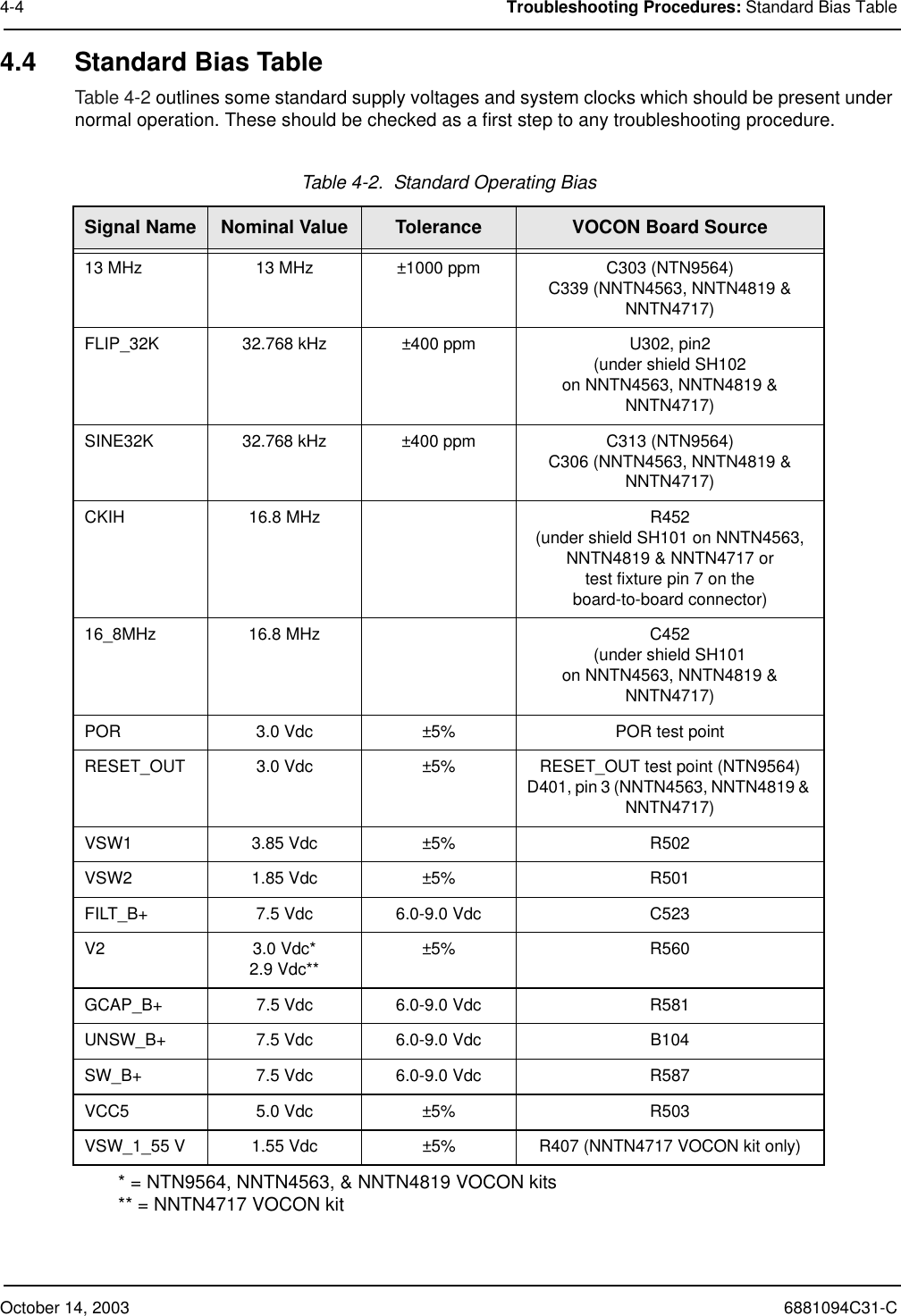
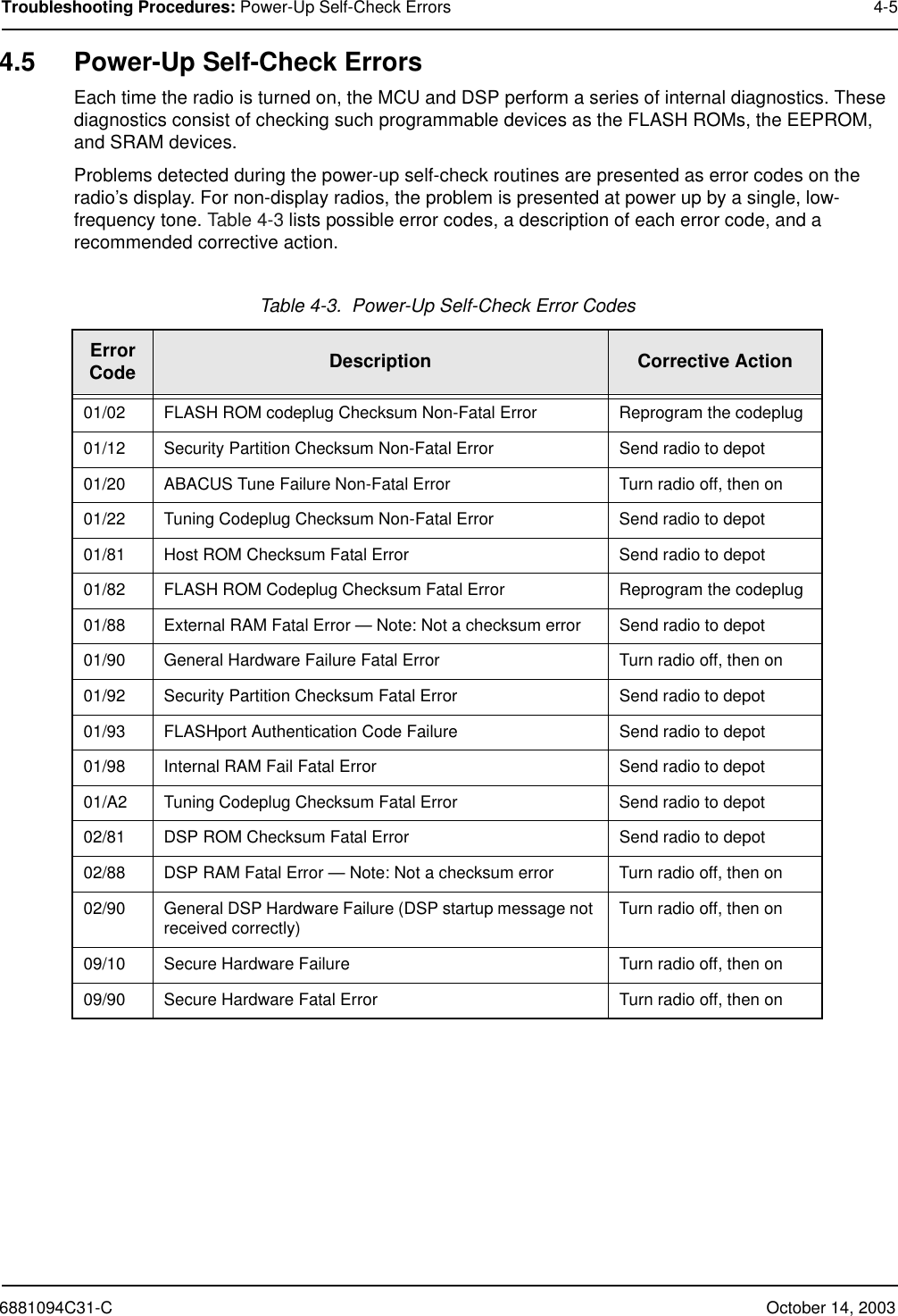
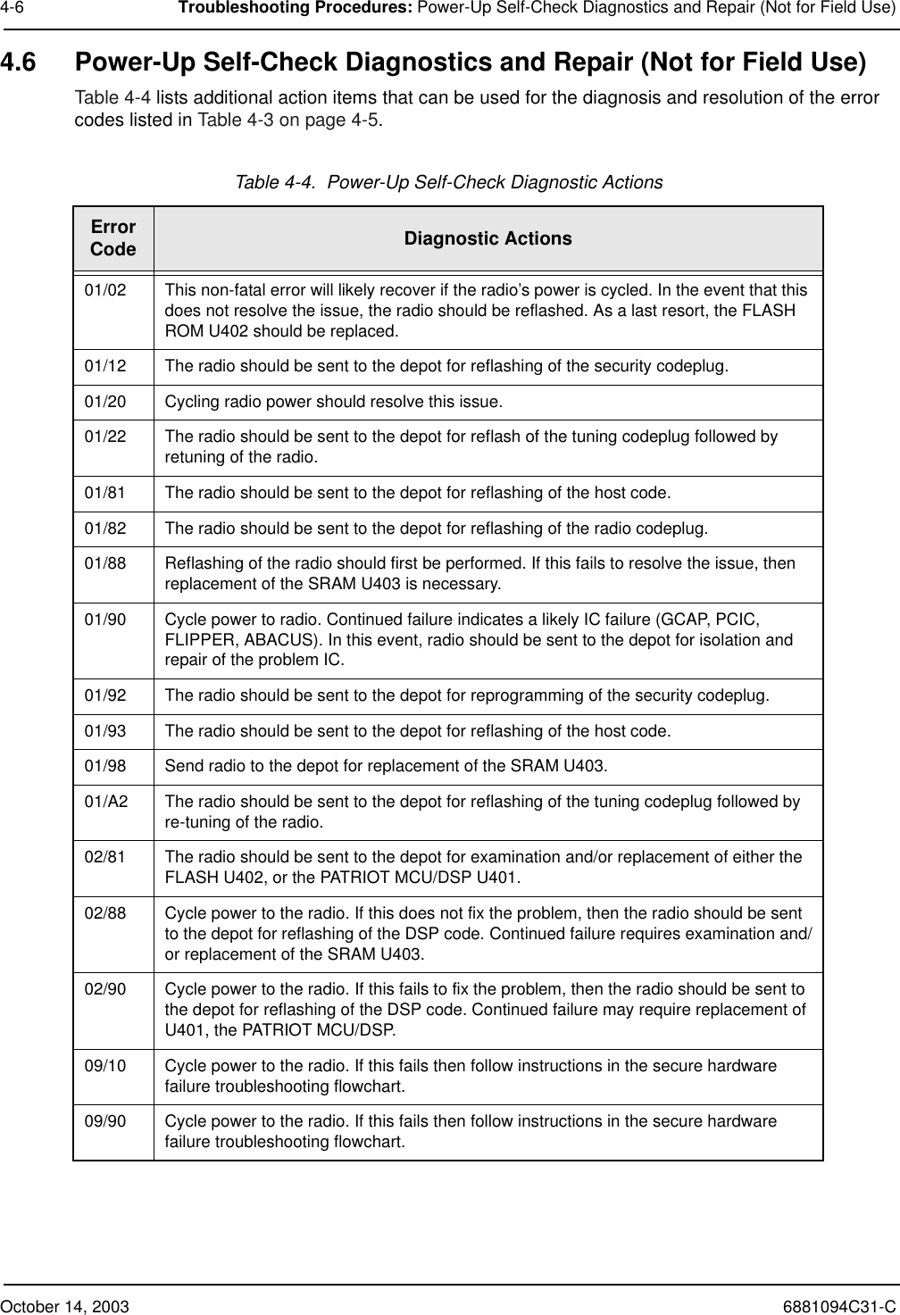
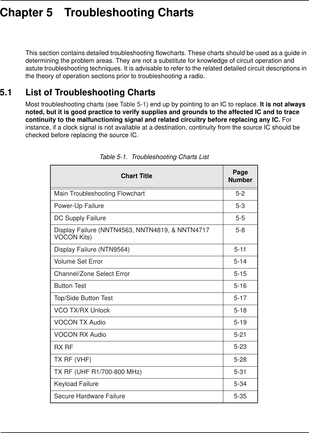
Contents
1.
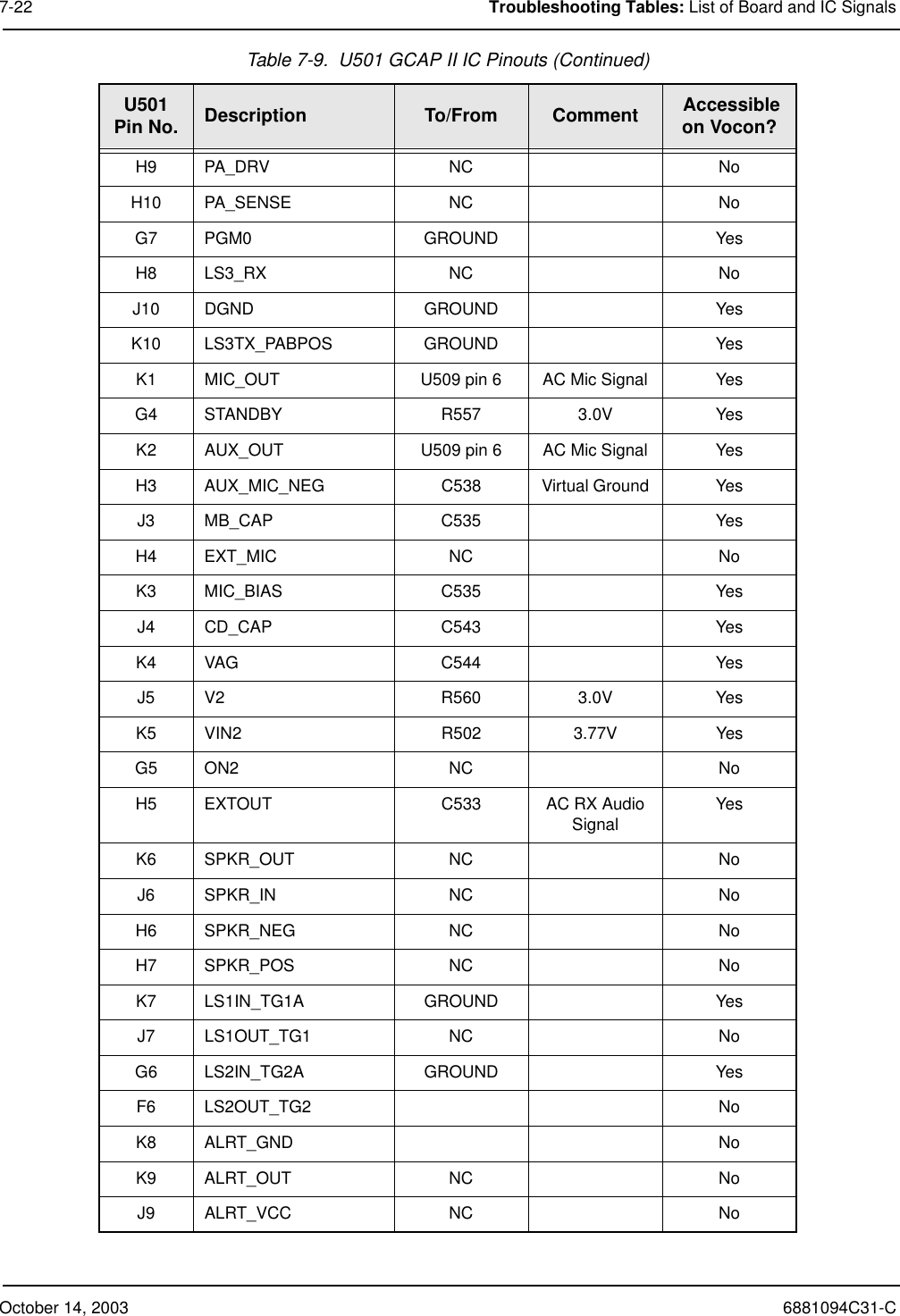
users manual
2.
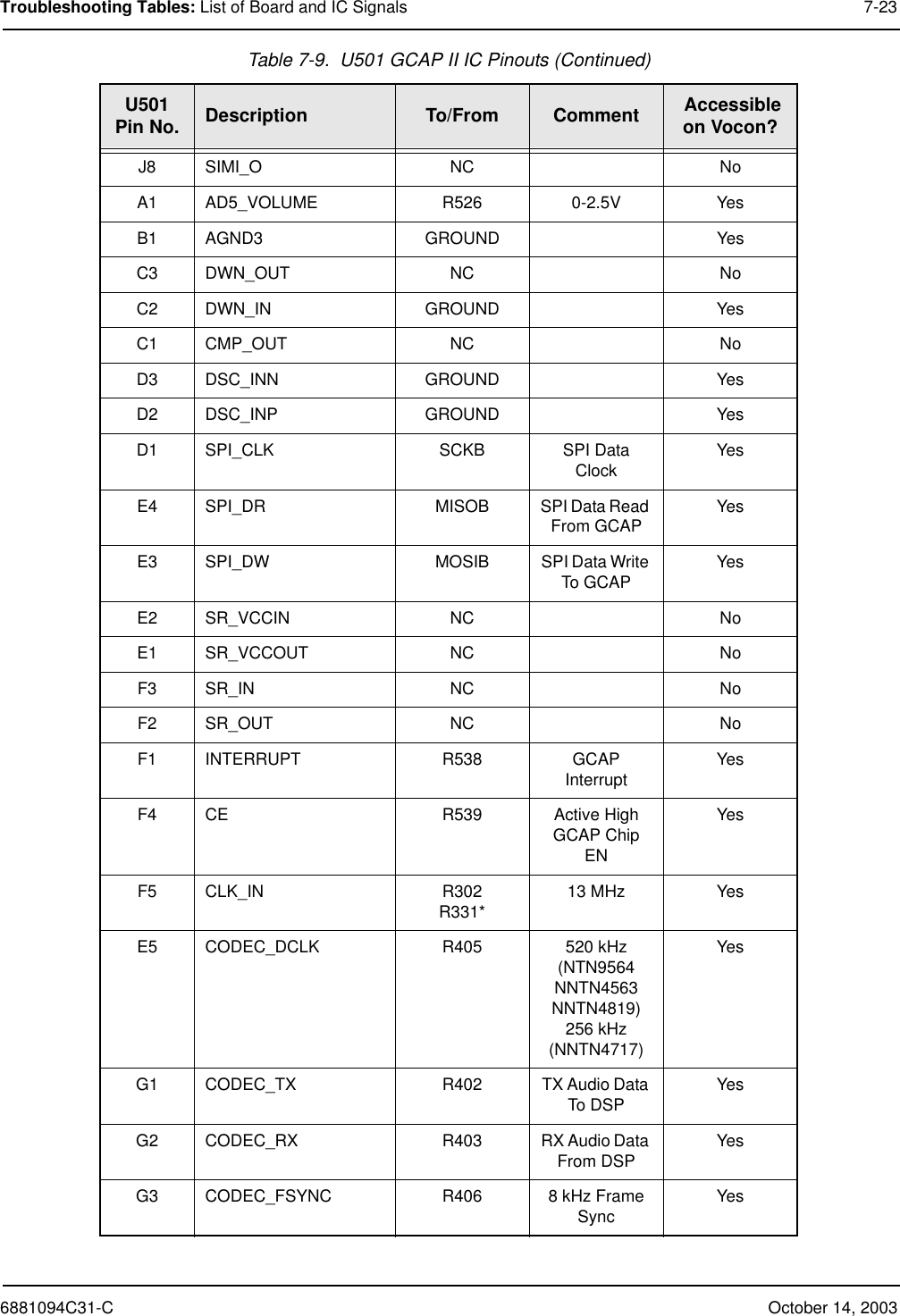
usrs maual 2
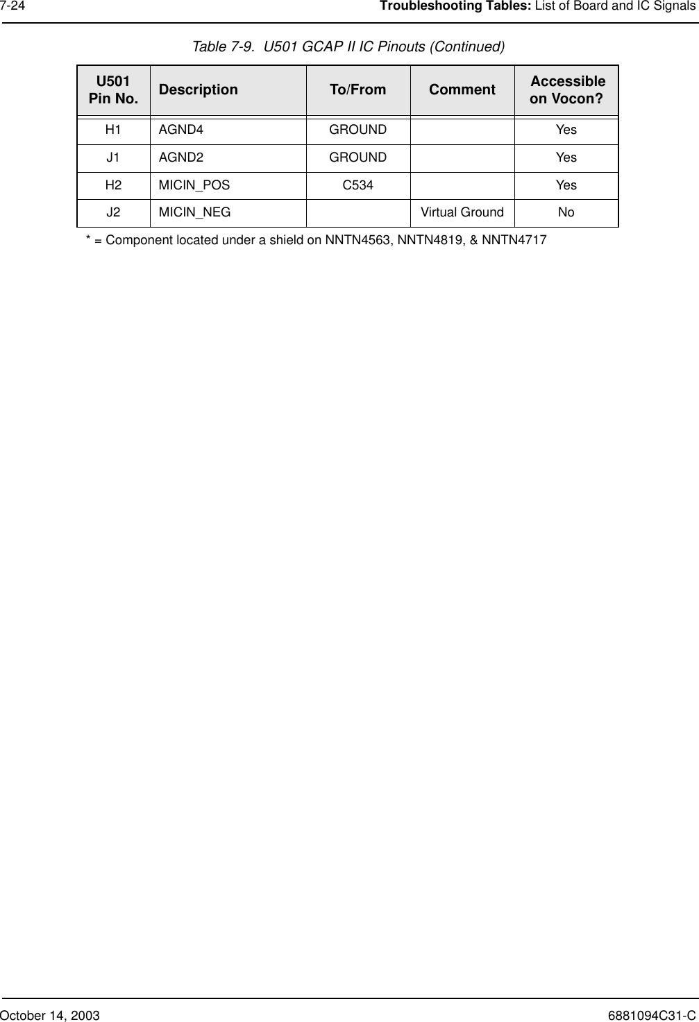
users manual
Navigation menu
Upload a User Manual
Namespaces
Wiki Guide
HTML
PDF
Info
Views
User Manual
Discussion / Help
Navigation