Technisonic T1088A 800 rf modular User Manual users manual
Technisonic Industries Limited 800 rf modular users manual
Contents
- 1. users manual
- 2. usrs maual 2
users manual
ASTRO® XTS™ 5000
VHF
UHF Range 1
700 — 800 MHz
Digital Portable Radios
Detailed Service Manual

Title Page ASTRO® XTS™ 5000
VHF/UHF Range 1/700–800 MHz
Digital Portable Radios
Detailed Service Manual
Motorola, Inc.
8000 West Sunrise Boulevard
Fort Lauderdale, Florida 33322 6881094C31-C

Foreword
The information contained in this manual relates to all ASTRO® XTS™ 5000 digital portable radios, unless otherwise
specified. This manual provides sufficient information to enable qualified service shop technicians to troubleshoot and
repair an ASTRO XTS 5000 digital portable radio to the component level.
For details on the operation of the radio or level 1 or 2 maintenance procedures, refer to the applicable manuals, which are
available separately. A list of related publications is provided in the section, “Related Publications,” on page xii.
Product Safety and RF Exposure Compliance
ATTENTION!
This radio is restricted to occupational use only to satisfy FCC RF energy exposure requirements.
Before using this product, read the RF energy awareness information and operating instructions in the
Product Safety and RF Exposure booklet enclosed with your radio (Motorola Publication part number
6881095C98) to ensure compliance with RF energy exposure limits.
For a list of Motorola-approved antennas, batteries, and other accessories, visit the following web site
which lists approved accessories: <http://www.motorola.com/cgiss/index.shtml>
Manual Revisions
Changes which occur after this manual is printed are described in FMRs (Florida Manual Revisions). These FMRs provide
complete replacement pages for all added, changed, and deleted items, including pertinent parts list data, schematics, and
component layout diagrams. To obtain FMRs, contact the Customer Care and Services Division (refer to “Appendix A
Replacement Parts Ordering”).
Computer Software Copyrights
The Motorola products described in this manual may include copyrighted Motorola computer programs stored in
semiconductor memories or other media. Laws in the United States and other countries preserve for Motorola certain
exclusive rights for copyrighted computer programs, including, but not limited to, the exclusive right to copy or reproduce in
any form the copyrighted computer program. Accordingly, any copyrighted Motorola computer programs contained in the
Motorola products described in this manual may not be copied, reproduced, modified, reverse-engineered, or distributed in
any manner without the express written permission of Motorola. Furthermore, the purchase of Motorola products shall not
be deemed to grant either directly or by implication, estoppel, or otherwise, any license under the copyrights, patents or
patent applications of Motorola, except for the normal non-exclusive license to use that arises by operation of law in the
sale of a product.
Document Copyrights
No duplication or distribution of this document or any portion thereof shall take place without the express written permission
of Motorola. No part of this manual may be reproduced, distributed, or transmitted in any form or by any means, electronic
or mechanical, for any purpose without the express written permission of Motorola.
Disclaimer
The information in this document is carefully examined, and is believed to be entirely reliable. However, no responsibility is
assumed for inaccuracies. Furthermore, Motorola reserves the right to make changes to any products herein to improve
readability, function, or design. Motorola does not assume any liability arising out of the applications or use of any product
or circuit described herein; nor does it cover any license under its patent rights nor the rights of others.
Trademarks
MOTOROLA, the Stylized M logo, and ASTRO are registered in the US Patent & Trademark Office. All other product or
service names are the property of their respective owners.
© Motorola, Inc. 2003.
Before using this product, read the operating instructions
for safe usage contained in the Product Safety and RF
Exposure booklet enclosed with your radio.
!
C a u t i o n

Table of Contents
Foreword.........................................................................................................ii
Product Safety and RF Exposure Compliance............................................................................................ii
Manual Revisions ........................................................................................................................................ii
Computer Software Copyrights ...................................................................................................................ii
Document Copyrights..................................................................................................................................ii
Disclaimer....................................................................................................................................................ii
Trademarks .................................................................................................................................................ii
List of Figures ..............................................................................................vii
List of Tables .................................................................................................xi
Commercial Warranty .................................................................................xiii
Limited Warranty ...................................................................................................................................... xiii
MOTOROLA COMMUNICATION PRODUCTS.............................................................................. xiii
I. What This Warranty Covers And For How Long ................................................................... xiii
II. General Provisions............................................................................................................... xiii
III. State Law Rights .................................................................................................................xiv
IV. How To Get Warranty Service ............................................................................................xiv
V. What This Warranty Does Not Cover...................................................................................xiv
VI. Patent And Software Provisions ..........................................................................................xv
VII. Governing Law....................................................................................................................xv
Model Numbering, Charts, and Specifications........................................xvii
Portable Radio Model Numbering System .............................................................................................. xvii
ASTRO XTS 5000 VHF Model Chart ..................................................................................................... xviii
ASTRO XTS 5000 R (Ruggedized) VHF Model Chart .............................................................................xix
ASTRO XTS 5000 UHF Range 1 Model Chart..........................................................................................xx
ASTRO XTS 5000 R (Ruggedized) UHF Range 1 Model Chart ..............................................................xxi
ASTRO XTS 5000 700–800 MHz Model Chart ....................................................................................... xxii
ASTRO XTS 5000 R (Ruggedized) 700–800 MHz Model Chart............................................................ xxiii
Specifications for VHF Radios................................................................................................................ xxiv
Specifications for UHF Range 1 Radios..................................................................................................xxv
Specifications for 700–800 MHz Radios................................................................................................. xxvi
Chapter 1 Introduction ......................................................................... 1-1
1.1 General.......................................................................................................................................... 1-1
1.2 Notations Used in This Manual...................................................................................................... 1-2
Chapter 2 Radio Power ........................................................................ 2-1

iv Table of Contents
October 14, 2003 6881094C31-C
2.1 General ..........................................................................................................................................2-1
2.2 DC Power Routing—Transceiver Board ........................................................................................2-3
2.3 DC Power Routing—VOCON Board..............................................................................................2-3
Chapter 3 Theory of Operation............................................................ 3-1
3.1 Transceiver Board..........................................................................................................................3-2
3.1.1 Interconnections................................................................................................................3-3
3.1.1.1 Battery Connector J3 ...............................................................................................3-3
3.1.1.2 VOCON Connector P1.............................................................................................3-3
3.1.1.3 Antenna Port J2 .......................................................................................................3-5
3.1.1.4 Serial EEPROM .......................................................................................................3-5
3.1.1.5 Power Conditioning Components ............................................................................3-5
3.1.2 Receiver............................................................................................................................3-5
3.1.2.1 Receiver Front End.................................................................................................. 3-6
3.1.2.2 Receiver Back End ..................................................................................................3-7
3.1.3 Transmitter........................................................................................................................3-8
3.1.3.1 Power Distribution....................................................................................................3-9
3.1.3.2 Driver Amplifier ........................................................................................................3-9
3.1.3.3 Power Amplifier Transistor Q107........................................................................... 3-10
3.1.3.4 Directional Coupler ................................................................................................3-10
3.1.3.5 Antenna Switch......................................................................................................3-10
3.1.3.6 Harmonic Filter.......................................................................................................3-10
3.1.3.7 RF Detectors D101 and D102................................................................................3-11
3.1.3.8 Summing Amplifier U106 .......................................................................................3-11
3.1.3.9 Power-Control IC (PCIC) U104..............................................................................3-11
3.1.4 Frequency Generation Unit (FGU)..................................................................................3-13
3.1.4.1 Reference Oscillator Y200 .....................................................................................3-13
3.1.4.2 Fractional-N Frequency Synthesizer (FracN) IC U202 ..........................................3-14
3.1.4.3 Loop Filter ..............................................................................................................3-15
3.1.4.4 VCO Buffer IC (VCOBIC).......................................................................................3-15
3.2 VOCON Board .............................................................................................................................3-16
3.2.1 Interconnections..............................................................................................................3-16
3.2.1.1 Universal Connector J101......................................................................................3-17
3.2.1.2 Encryption Connector J701....................................................................................3-17
3.2.1.3 Keypad Module Connector P107 ...........................................................................3-17
3.2.1.4 RF Interface Connector P201 ................................................................................3-17
3.2.1.5 Display Module Connector P301 ...........................................................................3-17
3.2.2 Controller and Memory ...................................................................................................3-17
3.2.2.1 Patriot IC U401 ......................................................................................................3-18
3.2.2.2 Static RAM (SRAM) U403......................................................................................3-20
3.2.2.3 FLASH Memory U402............................................................................................3-21
3.2.3 Audio and Power.............................................................................................................3-22
3.2.3.1 GCAP II IC U501....................................................................................................3-22
3.2.3.2 5 V Regulator U505 ............................................................................................... 3-23
3.2.3.3 1.55 V Regulator....................................................................................................3-23
3.2.3.4 Audio Pre-Amplifier U502 ......................................................................................3-24
3.2.3.5 Audio Power Amplifier U503..................................................................................3-24
3.2.3.6 EEPOT U509 .........................................................................................................3-24
3.2.4 Interface Support ............................................................................................................3-24
3.2.4.1 Flipper IC U301......................................................................................................3-25
3.2.4.2 ESD Protection Circuitry ........................................................................................3-27
3.2.4.3 Universal Connector Interface Circuitry .................................................................3-28

Table of Contents v
6881094C31-C October 14, 2003
3.2.4.4 Display Module ...................................................................................................... 3-29
3.2.4.5 Keypad Module...................................................................................................... 3-30
3.2.4.6 Controls and Control Top Flex............................................................................... 3-30
3.2.4.7 System Clocks....................................................................................................... 3-31
3.2.5 VOCON Audio Paths ...................................................................................................... 3-32
3.2.5.1 Transmit Audio Path .............................................................................................. 3-32
3.2.5.2 Receive Audio Path ............................................................................................... 3-33
3.2.6 Radio Power-Up/Power-Down Sequence....................................................................... 3-33
3.3 Encryption Module ....................................................................................................................... 3-34
Chapter 4 Troubleshooting Procedures............................................. 4-1
4.1 Handling Precautions..................................................................................................................... 4-1
4.2 Recommended Service Tools........................................................................................................ 4-2
4.3 Voltage Measurement and Signal Tracing..................................................................................... 4-3
4.4 Standard Bias Table ...................................................................................................................... 4-4
4.5 Power-Up Self-Check Errors ......................................................................................................... 4-5
4.6 Power-Up Self-Check Diagnostics and Repair (Not for Field Use)................................................ 4-6
Chapter 5 Troubleshooting Charts ..................................................... 5-1
5.1 List of Troubleshooting Charts....................................................................................................... 5-1
5.2 Main Troubleshooting Flowchart.................................................................................................... 5-2
5.3 Power-Up Failure........................................................................................................................... 5-3
5.4 DC Supply Failure.......................................................................................................................... 5-5
5.5 Display Failure (NNTN4563, NNTN4819, & NNTN4717 VOCON Kits) ......................................... 5-8
5.6 Display Failure (NTN9564) .......................................................................................................... 5-11
5.7 Volume Set Error ......................................................................................................................... 5-14
5.8 Channel/Zone Select Error .......................................................................................................... 5-15
5.9 Button Test .................................................................................................................................. 5-16
5.10 Top/Side Button Test ................................................................................................................... 5-17
5.11 VCO TX/RX Unlock ..................................................................................................................... 5-18
5.12 VOCON TX Audio........................................................................................................................ 5-19
5.13 VOCON RX Audio ....................................................................................................................... 5-21
5.14 RX RF .......................................................................................................................................... 5-23
5.15 TX RF (VHF)................................................................................................................................ 5-28
5.16 TX RF (UHF R1/700-800 MHz) ...................................................................................................5-31
5.17 Keyload Failure............................................................................................................................ 5-34
5.18 Secure Hardware Failure............................................................................................................. 5-35
Chapter 6 Troubleshooting Waveforms ............................................. 6-1
6.1 List of Waveforms .......................................................................................................................... 6-1
6.2 13 MHz Clock ................................................................................................................................ 6-2
6.3 16.8 MHz Buffer Input and Output................................................................................................. 6-3
6.4 32.768 kHz Clock Outputs............................................................................................................. 6-4
6.5 SPI B Data..................................................................................................................................... 6-5
6.6 Receive Serial Audio Port (SAP) ................................................................................................... 6-6
6.7 Receive Baseband Interface Port (RX BBP) ................................................................................. 6-7
6.8 Transmit Baseband Interface Port (TX BBP)................................................................................. 6-8

vi Table of Contents
October 14, 2003 6881094C31-C
Chapter 7 Troubleshooting Tables ..................................................... 7-1
7.1 List of Board and IC Signals .......................................................................................................... 7-1
Chapter 8 Schematics, Board Overlays, and Parts Lists.................. 8-1
8.1 List of Transceiver Schematics and Board Overlays .....................................................................8-1
8.2 List of VOCON Schematics and Board Overlays...........................................................................8-1
8.3 Transceiver (RF) Boards................................................................................................................8-3
8.4 VOCON Boards ........................................................................................................................... 8-79
Appendix A Replacement Parts Ordering..............................................A-1
A.1 Basic Ordering Information ............................................................................................................A-1
A.2 Transceiver Board and VOCON Board Ordering Information........................................................A-1
A.3 Motorola Online..............................................................................................................................A-1
A.4 Mail Orders ....................................................................................................................................A-1
A.5 Telephone Orders..........................................................................................................................A-2
A.6 Fax Orders.....................................................................................................................................A-2
A.7 Parts Identification .........................................................................................................................A-2
A.8 Product Customer Service.............................................................................................................A-2
Glossary.........................................................................................Glossary-1
Index.....................................................................................................Index-1

List of Figures vii
6881094C31-C October 14, 2003
List of Figures
Figure 2-1. DC Power Distribution—UHF Range 1 and 700–800 MHz Radios ...................................... 2-2
Figure 2-2. DC Power Distribution—VHF Radios.................................................................................... 2-2
Figure 3-1. XTS 5000 Overall Block Diagram ......................................................................................... 3-1
Figure 3-2. Transceiver (VHF) Block Diagram (Power and Control Omitted) ......................................... 3-2
Figure 3-3. Transceiver (UHF Range 1 and 700–800 MHz) Block Diagram
(Power and Control Omitted) ................................................................................................ 3-3
Figure 3-4. Receiver Block Diagram ....................................................................................................... 3-5
Figure 3-5. Abacus III (AD9874) Functional Block Diagram (from data sheet) ....................................... 3-7
Figure 3-6. Transmitter Block Diagram ................................................................................................... 3-9
Figure 3-7. VOCON Board Interconnections.........................................................................................3-16
Figure 3-8. Patriot EIM and Memory Block Diagram............................................................................. 3-21
Figure 3-9. Universal (Side) Connector................................................................................................. 3-28
Figure 3-10. VOCON Board Connector—J101 ....................................................................................... 3-28
Figure 3-11. Control Top Flex.................................................................................................................. 3-31
Figure 3-12. VOCON Transmit Audio Path ............................................................................................. 3-32
Figure 3-13. VOCON Receive Audio Path .............................................................................................. 3-33
Figure 6-1. 13 MHz Clock Waveform ...................................................................................................... 6-2
Figure 6-2. 16.8 MHz Buffer Input and Output Waveforms ..................................................................... 6-3
Figure 6-3. 32.768 kHz Clock Outputs Waveforms ................................................................................. 6-4
Figure 6-4. SPI B Data Waveforms ......................................................................................................... 6-5
Figure 6-5. Receive Serial Audio Port (SAP) Waveforms ....................................................................... 6-6
Figure 6-6. Receive Baseband Interface Port (RX BBP) Waveforms ..................................................... 6-7
Figure 6-7. Transmit Baseband Interface Port (TX BBP) Waveforms ..................................................... 6-8
Figure 8-1. NUF3577 700–800 MHz Transceiver (RF) Board Overall Circuit Schematic ....................... 8-3
Figure 8-2. NUF3577 700–800 MHz Antenna Switch and Harmonic Filter Circuits................................ 8-4
Figure 8-3. NUF3577 700–800 MHz Receiver Front End Circuit............................................................ 8-5
Figure 8-4. NUF3577 700–800 MHz Receiver Back End Circuit ............................................................ 8-6
Figure 8-5. NUF3577 700–800 MHz Transmitter and Automatic Level Control Circuits......................... 8-7
Figure 8-6. NUF3577 700–800 MHz Frequency Generation Unit (Synthesizer) Circuit—1 of 2............. 8-8
Figure 8-7. NUF3577 700–800 MHz Frequency Generation Unit (VCO) Circuit—2 of 2........................ 8-9
Figure 8-8. NUF3577 700–800 MHz Transceiver (RF) Board Layout—Side 1..................................... 8-10
Figure 8-9. NUF3577 700–800 MHz Transceiver (RF) Board Layout—Side 2..................................... 8-11
Figure 8-10. NUF3577C 700–800 MHz Transceiver (RF) Board Overall Circuit Schematic................... 8-17
Figure 8-11. NUF3577C 700–800 MHz Antenna Switch and Harmonic Filter Circuits ........................... 8-18
Figure 8-12. NUF3577C 700–800 MHz Receiver Front End Circuit ....................................................... 8-19
Figure 8-13. NUF3577C 700–800 MHz Receiver Back End Circuit........................................................ 8-20
Figure 8-14. NUF3577C 700–800 MHz Transmitter and Automatic Level Control Circuits .................... 8-21
Figure 8-15. NUF3577C 700–800 MHz Frequency Generation Unit (Synthesizer) Circuit..................... 8-22
Figure 8-16. NUF3577C 700–800 MHz Frequency Generation Unit (VCO) Circuit................................ 8-23
Figure 8-17. NUF3577C 700–800 MHz Transceiver (RF) Board Layout—Side 1 .................................. 8-24
Figure 8-18. NUF3577C 700–800 MHz Transceiver (RF) Board Layout—Side 2 .................................. 8-25
Figure 8-19. NLD8910B VHF Transceiver (RF) Board Overall Circuit Schematic .................................. 8-31
Figure 8-20. NLD8910B VHF DC Power Circuits.................................................................................... 8-32
Figure 8-21. NLD8910B VHF Antenna Switch and Harmonic Filter Circuits........................................... 8-33
Figure 8-22. NLD8910B VHF Receiver Front End Circuit....................................................................... 8-34
Figure 8-23. NLD8910B VHF Receiver Amplifier and Filter Circuit......................................................... 8-35
Figure 8-24. NLD8910B VHF Mixer and IF Filter Circuits ....................................................................... 8-36
Figure 8-25. NLD8910B VHF Receiver Back End Circuit ....................................................................... 8-37

viii List of Figures
October 14, 2003 6881094C31-C
Figure 8-26. NLD8910B VHF Transmitter and Automatic Level Control Circuits ...................................8-38
Figure 8-27. NLD8910B VHF Frequency Generation Unit (Synthesizer) Circuit.....................................8-39
Figure 8-28. NLD8910B VHF Frequency Generation Unit (VCO) Circuit................................................8-40
Figure 8-29. NLD8910B VHF Transceiver (RF) Board Layout—Side 1 ..................................................8-41
Figure 8-30. NLD8910B VHF Transceiver (RF) Board Layout—Side 2 ..................................................8-42
Figure 8-31. NLE4272A UHF Range 1 Transceiver (RF) Board Overall Circuit Schematic....................8-48
Figure 8-32. NLE4272A UHF Range 1 Antenna Switch and Harmonic Filter Circuits ............................8-49
Figure 8-33. NLE4272A UHF Range 1 Receiver Front End (RX_FE) Circuit..........................................8-50
Figure 8-34. NLE4272A UHF Range 1 Receiver Back End (RX_BE) Circuit..........................................8-51
Figure 8-35. NLE4272A UHF Range 1 Transmitter Power Amplifier and Automatic Level Control (TX_ALC)
Circuit..................................................................................................................................8-52
Figure 8-36. NLE4272A UHF Range 1 Frequency Generation Unit (Synthesizer) Circuit ......................8-53
Figure 8-37. NLE4272A UHF Range 1 Frequency Generation Unit (VCO) Circuit ................................8-54
Figure 8-38. NLE4272A UHF Range 1 Transceiver (RF) Board Layout—Side 1....................................8-55
Figure 8-39. NLE4272A UHF Range 1 Transceiver (RF) Board Layout—Side 2....................................8-56
Figure 8-40. NLE4278A UHF Range 1 Transceiver (RF) Board Overall Circuit Schematic....................8-64
Figure 8-41. NLE4278A UHF Range 1 Antenna Switch and Harmonic Filter Circuits ............................8-65
Figure 8-42. NLE4278A UHF Range 1 Receiver Front End Circuit.........................................................8-66
Figure 8-43. NLE4278A UHF Range 1 Receiver Back End Circuit......................................................... 8-67
Figure 8-44. NLE4278A UHF Range 1 Transmitter Power Amplifier and Automatic Level Control
Circuit..................................................................................................................................8-68
Figure 8-45. NLE4278A UHF Range 1 Frequency Unit (Synthesizer) Circuit.........................................8-69
Figure 8-46. NLE4278A UHF Range 1 Frequency Generation Unit (VCO) Circuit .................................8-70
Figure 8-47. NLE4278A UHF Range 1 Transceiver (RF) Board Layout—Side 1....................................8-71
Figure 8-48. NLE4278A UHF Range 1 Transceiver (RF) Board Layout—Side 2....................................8-72
Figure 8-49. NTN9564B VOCON Board Overall Schematic—1 of 2.......................................................8-79
Figure 8-50. NTN9564B VOCON Board Overall Schematic—2 of 2.......................................................8-80
Figure 8-51. NTN9564B VOCON Universal Connector Circuit ...............................................................8-81
Figure 8-52. NTN9564B VOCON Flipper Circuit.....................................................................................8-82
Figure 8-53. NTN9564B VOCON Controller and Memory Circuits—1 of 2.............................................8-83
Figure 8-54. NTN9564B VOCON Controller and Memory Circuits—2 of 2.............................................8-84
Figure 8-55. NTN9564B VOCON Audio and DC Circuits........................................................................8-85
Figure 8-56. NTN9564B VOCON Board Layout—Side 1........................................................................8-86
Figure 8-57. NTN9564B VOCON Board Layout—Side 2........................................................................8-87
Figure 8-58. NTN9564C VOCON Board Overall Schematic—1 of 2.......................................................8-93
Figure 8-59. NTN9564C VOCON Board Overall Schematic—2 of 2.......................................................8-94
Figure 8-60. NTN9564C VOCON Universal Connector Circuit ...............................................................8-95
Figure 8-61. NTN9564C VOCON Flipper Circuit.....................................................................................8-96
Figure 8-62. NTN9564C VOCON Controller and Memory Circuits—1 of 2.............................................8-97
Figure 8-63. NTN9564C VOCON Controller and Memory Circuits—2 of 2.............................................8-98
Figure 8-64. NTN9564C VOCON Audio and DC Circuits........................................................................8-99
Figure 8-65. NTN9564C VOCON Board Layout—Side 1......................................................................8-100
Figure 8-66. NTN9564C VOCON Board Layout—Side 2......................................................................8-101
Figure 8-67. NNTN4563A/B VOCON Board Overall Schematic—1 of 2...............................................8-107
Figure 8-68. NNTN4563A/B VOCON Board Overall Schematic—2 of 2...............................................8-108
Figure 8-69. NNTN4563A/B VOCON Universal Connector Circuit .......................................................8-109
Figure 8-70. NNTN4563A/B VOCON Flipper Circuit.............................................................................8-110
Figure 8-71. NNTN4563A/B VOCON Controller and Memory Circuits—1 of 2.....................................8-111
Figure 8-72. NNTN4563A/B VOCON Controller and Memory Circuits—2 of 2.....................................8-112
Figure 8-73. NNTN4563A/B VOCON Audio and DC Circuits................................................................8-113
Figure 8-74. NNTN4563A/B VOCON Board Layout—Side 1................................................................8-114
Figure 8-75. NNTN4563A/B VOCON Board Layout—Side 2................................................................8-115
Figure 8-76. NNTN4819A VOCON Board Overall Schematic—Sheet 1 of 2........................................8-122
Figure 8-77. NNTN4819A VOCON Board Overall Schematic—Sheet 2 of 2........................................8-123

List of Figures ix
6881094C31-C October 14, 2003
Figure 8-78. NNTN4819A VOCON Universal Connector and ESD Circuits ......................................... 8-124
Figure 8-79. NNTN4819A VOCON Flipper Circuit ................................................................................ 8-125
Figure 8-80. NNTN4819A VOCON Controller and Memory Circuits—Sheet 1 of 2.............................. 8-126
Figure 8-81. NNTN4819A VOCON Controller and Memory Circuits—Sheet 2 of 2.............................. 8-127
Figure 8-82. NNTN4819A VOCON Audio/DC Circuits.......................................................................... 8-128
Figure 8-83. NNTN4819A VOCON Board Layout—Side 1 ................................................................... 8-129
Figure 8-84. NNTN4819A VOCON Board Layout—Side 2 ................................................................... 8-130
Figure 8-85. NNTN4717D VOCON Board Overall Schematic—Sheet 1 of 2 ....................................... 8-136
Figure 8-86. NNTN4717D VOCON Board Overall Schematic—Sheet 2 of 2 ....................................... 8-137
Figure 8-87. NNTN4717D VOCON Board Universal Connector Circuit Schematic.............................. 8-138
Figure 8-88. NNTN4717D VOCON Board Flipper Circuit ..................................................................... 8-139
Figure 8-89. NNTN4717D VOCON Board Controller and Memory Circuits—Sheet 1 of 2................... 8-140
Figure 8-90. NNTN4717D VOCON Board Controller and Memory Circuits—Sheet 2 of 2................... 8-141
Figure 8-91. NNTN4717D VOCON Board Audio/DC Circuits ............................................................... 8-142
Figure 8-92. NNTN4717D VOCON Board Layout—Side 1................................................................... 8-143
Figure 8-93. NNTN4717D VOCON Board Layout—Side 2................................................................... 8-144

xList of Figures
October 14, 2003 6881094C31-C

List of Tables xi
6881094C31-C October 14, 2003
List of Tables
Table 2-1. Conventional Batteries.......................................................................................................... 2-1
Table 2-2. Smart Batteries ..................................................................................................................... 2-1
Table 2-3. Transceiver Voltage Regulators............................................................................................ 2-3
Table 2-4. VOCON Board DC Power Distribution.................................................................................. 2-4
Table 3-1. Battery Connector J3 ............................................................................................................ 3-3
Table 3-2. VOCON Connector P1.......................................................................................................... 3-4
Table 3-3. Power Control IC (U104) Pin Descriptions.......................................................................... 3-11
Table 3-4. Audio PA Status .................................................................................................................. 3-24
Table 3-5. Option-Select Functions ..................................................................................................... 3-29
Table 3-6. Encryption Module Software Kits and Algorithms ............................................................... 3-34
Table 4-1. Recommended Service Tools ............................................................................................... 4-2
Table 4-2. Standard Operating Bias....................................................................................................... 4-4
Table 4-3. Power-Up Self-Check Error Codes.......................................................................................4-5
Table 4-4. Power-Up Self-Check Diagnostic Actions............................................................................. 4-6
Table 5-1. Troubleshooting Charts List .................................................................................................. 5-1
Table 6-1. List of Waveforms ................................................................................................................. 6-1
Table 7-1. List of Tables of Board and IC Signals.................................................................................. 7-1
Table 7-2. J101 VOCON Board to Controls Flex Assembly................................................................... 7-1
Table 7-3. J107 VOCON Board to Keypad Module ............................................................................... 7-3
Table 7-4. J701 VOCON Board to Encryption Module........................................................................... 7-3
Table 7-5. U402 FLASH Pinouts............................................................................................................ 7-5
Table 7-6. U403 SRAM Pinouts............................................................................................................. 7-7
Table 7-7. U401 Patriot MCU/DSP IC Pinouts.......................................................................................7-9
Table 7-8. U301 Flipper IC Pinouts...................................................................................................... 7-18
Table 7-9. U501 GCAP II IC Pinouts.................................................................................................... 7-20
Table 8-1. List of Transceiver Schematics and Board Overlays ............................................................ 8-1
Table 8-2. List of VOCON Schematics and Board Overlays.................................................................. 8-1

xii List of Tables
October 14, 2003 6881094C31-C
Related Publications
ASTRO XTS 5000 Digital Portable Radio Model I User Guide ................................................. 6881094C25
ASTRO XTS 5000 Digital Portable Radio Model II User Guide ................................................ 6881094C26
ASTRO XTS 5000 Digital Portable Radio Model III User Guide ............................................... 6881094C27
ASTRO XTS 5000 VHF/UHF Range 1/700–800 MHz Digital Portable Radios
Basic Service Manual ......................................................................................................... 6881094C28
Factory Mutual Approval XTS 5000 Product Listing Manual Supplement................................. 6881094C78
Commercial Warranty
Limited Warranty
MOTOROLA COMMUNICATION PRODUCTS
I. What This Warranty Covers And For How Long
MOTOROLA INC. (“MOTOROLA”) warrants the MOTOROLA manufactured Communication
Products listed below (“Product”) against defects in material and workmanship under normal use and
service for a period of time from the date of purchase as scheduled below:
Motorola, at its option, will at no charge either repair the Product (with new or reconditioned parts),
replace it (with a new or reconditioned Product), or refund the purchase price of the Product during
the warranty period provided it is returned in accordance with the terms of this warranty. Replaced
parts or boards are warranted for the balance of the original applicable warranty period. All replaced
parts of Product shall become the property of MOTOROLA.
This express limited warranty is extended by MOTOROLA to the original end user purchaser only
and is not assignable or transferable to any other party. This is the complete warranty for the Product
manufactured by MOTOROLA. MOTOROLA assumes no obligations or liability for additions or
modifications to this warranty unless made in writing and signed by an officer of MOTOROLA.
Unless made in a separate agreement between MOTOROLA and the original end user purchaser,
MOTOROLA does not warrant the installation, maintenance or service of the Product.
MOTOROLA cannot be responsible in any way for any ancillary equipment not furnished by
MOTOROLA which is attached to or used in connection with the Product, or for operation of the
Product with any ancillary equipment, and all such equipment is expressly excluded from this
warranty. Because each system which may use the Product is unique, MOTOROLA disclaims
liability for range, coverage, or operation of the system as a whole under this warranty.
II. General Provisions
This warranty sets forth the full extent of MOTOROLA’s responsibilities regarding the Product.
Repair, replacement or refund of the purchase price, at MOTOROLA’s option, is the exclusive
remedy. THIS WARRANTY IS GIVEN IN LIEU OF ALL OTHER EXPRESS WARRANTIES. IMPLIED
WARRANTIES, INCLUDING WITHOUT LIMITATION, IMPLIED WARRANTIES OF
MERCHANTABILITY AND FITNESS FOR A PARTICULAR PURPOSE, ARE LIMITED TO THE
DURATION OF THIS LIMITED WARRANTY. IN NO EVENT SHALL MOTOROLA BE LIABLE FOR
DAMAGES IN EXCESS OF THE PURCHASE PRICE OF THE PRODUCT, FOR ANY LOSS OF
USE, LOSS OF TIME, INCONVENIENCE, COMMERCIAL LOSS, LOST PROFITS OR SAVINGS
OR OTHER INCIDENTAL, SPECIAL OR CONSEQUENTIAL DAMAGES ARISING OUT OF THE
USE OR INABILITY TO USE SUCH PRODUCT, TO THE FULL EXTENT SUCH MAY BE
DISCLAIMED BY LAW.
ASTRO XTS 5000 Digital Portable Units One (1) Year
Product Accessories One (1) Year

October 14, 2003 6881094C31-C
xiv Commercial Warranty
III. State Law Rights
SOME STATES DO NOT ALLOW THE EXCLUSION OR LIMITATION OF INCIDENTAL OR
CONSEQUENTIAL DAMAGES OR LIMITATION ON HOW LONG AN IMPLIED WARRANTY
LASTS, SO THE ABOVE LIMITATION OR EXCLUSIONS MAY NOT APPLY.
This warranty gives specific legal rights, and there may be other rights which may vary from state to
state.
IV. How To Get Warranty Service
You must provide proof of purchase (bearing the date of purchase and Product item serial number)
in order to receive warranty service and, also, deliver or send the Product item, transportation and
insurance prepaid, to an authorized warranty service location. Warranty service will be provided by
Motorola through one of its authorized warranty service locations. If you first contact the company
which sold you the Product, it can facilitate your obtaining warranty service. You can also call
Motorola at 1-888-567-7347 US/Canada.
V. What This Warranty Does Not Cover
A. Defects or damage resulting from use of the Product in other than its normal and customary
manner.
B. Defects or damage from misuse, accident, water, or neglect.
C. Defects or damage from improper testing, operation, maintenance, installation, alteration,
modification, or adjustment.
D. Breakage or damage to antennas unless caused directly by defects in material workmanship.
E. A Product subjected to unauthorized Product modifications, disassemblies or repairs
(including, without limitation, the addition to the Product of non-Motorola supplied equipment)
which adversely affect performance of the Product or interfere with Motorola’s normal
warranty inspection and testing of the Product to verify any warranty claim.
F. Product which has had the serial number removed or made illegible.
G. Rechargeable batteries if:
• any of the seals on the battery enclosure of cells are broken or show evidence of
tampering.
• the damage or defect is caused by charging or using the battery in equipment or service
other than the Product for which it is specified.
H. Freight costs to the repair depot.
I. A Product which, due to illegal or unauthorized alteration of the software/firmware in the
Product, does not function in accordance with MOTOROLA’s published specifications or the
FCC type acceptance labeling in effect for the Product at the time the Product was initially
distributed from MOTOROLA.
J. Scratches or other cosmetic damage to Product surfaces that does not affect the operation of
the Product.
K. Normal and customary wear and tear.

6881094C31-C October 14, 2003
Commercial Warranty xv
VI. Patent And Software Provisions
MOTOROLA will defend, at its own expense, any suit brought against the end user purchaser to the
extent that it is based on a claim that the Product or parts infringe a United States patent, and
MOTOROLA will pay those costs and damages finally awarded against the end user purchaser in
any such suit which are attributable to any such claim, but such defense and payments are
conditioned on the following:
A. that MOTOROLA will be notified promptly in writing by such purchaser of any notice of such
claim;
B. that MOTOROLA will have sole control of the defense of such suit and all negotiations for its
settlement or compromise; and
C. should the Product or parts become, or in MOTOROLA’s opinion be likely to become, the
subject of a claim of infringement of a United States patent, that such purchaser will permit
MOTOROLA, at its option and expense, either to procure for such purchaser the right to
continue using the Product or parts or to replace or modify the same so that it becomes
noninfringing or to grant such purchaser a credit for the Product or parts as depreciated and
accept its return. The depreciation will be an equal amount per year over the lifetime of the
Product or parts as established by MOTOROLA.
MOTOROLA will have no liability with respect to any claim of patent infringement which is based
upon the combination of the Product or parts furnished hereunder with software, apparatus or
devices not furnished by MOTOROLA, nor will MOTOROLA have any liability for the use of ancillary
equipment or software not furnished by MOTOROLA which is attached to or used in connection with
the Product. The foregoing states the entire liability of MOTOROLA with respect to infringement of
patents by the Product or any parts thereof.
Laws in the United States and other countries preserve for MOTOROLA certain exclusive rights for
copyrighted MOTOROLA software such as the exclusive rights to reproduce in copies and distribute
copies of such Motorola software. MOTOROLA software may be used in only the Product in which
the software was originally embodied and such software in such Product may not be replaced,
copied, distributed, modified in any way, or used to produce any derivative thereof. No other use
including, without limitation, alteration, modification, reproduction, distribution, or reverse
engineering of such MOTOROLA software or exercise of rights in such MOTOROLA software is
permitted. No license is granted by implication, estoppel or otherwise under MOTOROLA patent
rights or copyrights.
VII. Governing Law
This Warranty is governed by the laws of the State of Illinois, USA.

October 14, 2003 6881094C31-C
xvi Commercial Warranty
Notes
6881094C31-C October 14, 2003
Portable Radio Model Numbering System xvii
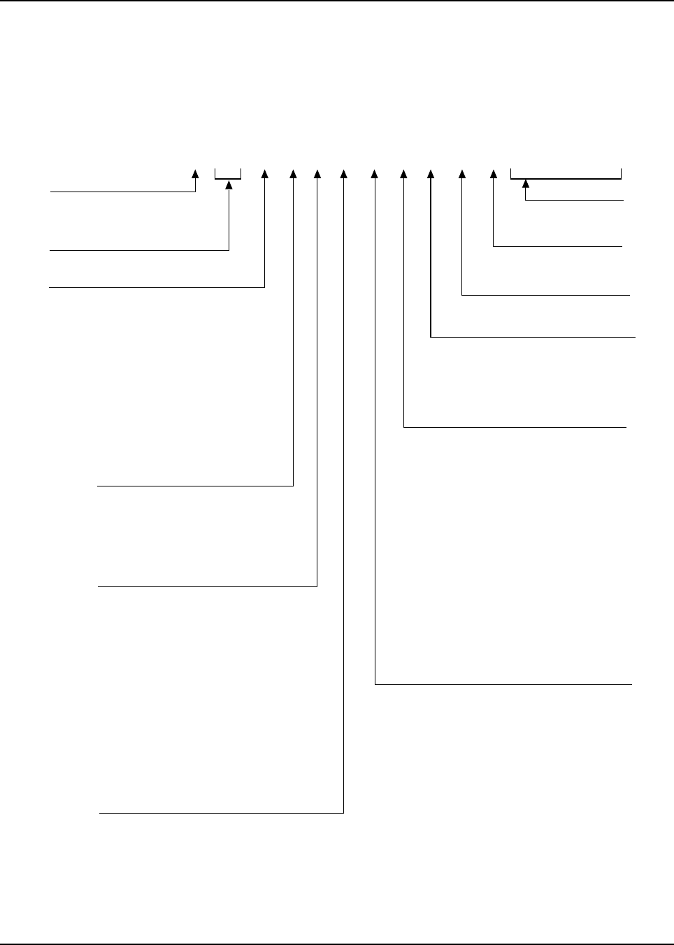
Model Numbering, Charts, and Specifications
Portable Radio Model Numbering System
Position 1 - Type of Unit
H = Hand-Held Portable
Positions 2 & 3 - Model Series
Position 4 - Frequency Band
Less than 29.7MHz
29.7 to 35.99MHz
36 to 41.99MHz
42 to 50MHz
66 to 80MHz
74 to 90MHz
Product Specific
136 to 162MHz
146 to 178MHz
174 to 210MHz
190 to 235MHz
336 to 410MHz
380 to 470MHz
438 to 482MHz
470 to 520MHz
Product Specific
764 to 870MHz
825 to 870MHz
896 to 941MHz
1.0 to 1.6GHz
1.5 to 2.0GHz
Values given represent range only; they are
not absolute.
Position 5 - Power Level
0 to 0.7 Watts
0.7 to 0.9 Watts
1.0 to 3.9 Watts
4.0 to 5.0 Watts
5.1 to 6.0 Watts
6.1 to 10 Watts
Position 6 - Physical Packages
RF Modem Operation
Receiver Only
Standard Control; No Display
Standard Control; With Display
Limited Keypad; No Display
Limited Keypad; With Display
Full Keypad; No Display
Full Keypad; With Display
Limited Controls; No Display
Limited Controls; Basic Display
Limited Controls; Limited Display
Rotary Controls; Standard Display
Enhanced Controls; Enhanced Display
Low Profile; No Display
Low Profile; Basic Display
Low Profile; Basic Display, Full Keypad
Position 7 - Channel Spacing
1 = 5kHz
2 = 6.25kHz
3 = 10kHz
4 = 12.5kHz
5 = 15kHz
6 = 20/25kHz
7 = 30kHz
9 = Variable/Programmable
Typical Model Number:
Position:
Position 8 - Primary Operation
Conventional/Simplex
Conventional/Duplex
Trunked Twin Type
Dual Mode Trunked
Dual Mode Trunked/Duplex
Trunked Type I
Trunked Type II
FDMA* Digital Dual Mode
TDMA** Digital Dual Mode
Single Sideband
Global Positioning Satellite Capable
Amplitude Companded Sideband (ACSB)
Programmable
* FDMA = Frequency Division Multiple Access
** TDMA = Time Division Multiple Access
Position 9 - Primary System Type
Conventional
Privacy Plus
Clear SMARTNET
Advanced Conventional Stat-Alert
Enhanced Privacy Plus
Nauganet 888 Series
Japan Specialized Mobile Radio (JSMR)
Multi-Channel Access (MCA)
CoveragePLUS
MPT1327* - Public
MPT1327* - Private
Radiocom
Tone Signalling
Binary Signalling
Phonenet
Programmable
Secure Conventional
Secure SMARTNET
* MPT = Ministry of Posts and Telecommunications
Position 10 - Feature Level
1 = Basic
2 = Limited Package
3 = Limited Plus
4 = Intermediate
5 = Standard Package
6 = Standard Plus
7 = Expanded Package
8 = Expanded Plus
9 = Full Feature/
Programmable
Position 11 - Version
Version Letter (Alpha) - Major Change
Position 12 -
Unique Model Variations
C = Cenelec
N = Standard Package
Positions 13 - 16
SP Model Suffix
123 4 56 7 8 910111213141516
H18 U CF 9 P W 7 A N S P 0 1
18 = XTS 5000
A
B
C
D
F
G
H
J
K
L
M
=
=
=
=
=
=
=
=
=
=
=
P
Q
R
S
T
U
V
W
Y
Z
=
=
=
=
=
=
=
=
=
=
A
B
C
D
E
F
=
=
=
=
=
=
A
B
C
D
E
F
G
H
J
K
L
M
N
P
Q
R
=
=
=
=
=
=
=
=
=
=
=
=
=
=
=
=
A
B
C
D
E
F
G
H
J
K
L
M
P
=
=
=
=
=
=
=
=
=
=
=
=
=
A
B
C
D
E
F
G
H
J
K
L
M
N
P
Q
W
X
Y
=
=
=
=
=
=
=
=
=
=
=
=
=
=
=
=
=
=
MAEPF-27620-O

October 14, 2003 6881094C31-C
xviii Portable Radio Model Numbering System
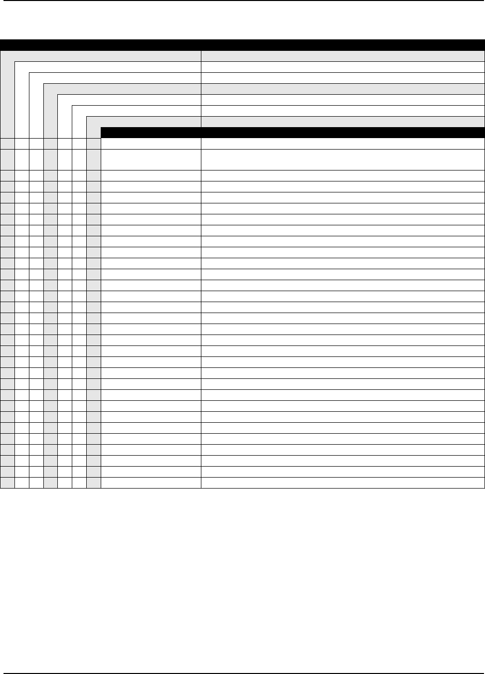
ASTRO XTS 5000 VHF Model Chart
MODEL NUMBER DESCRIPTION
H18KEC9PW5AN VHF 1-6 Watts ASTRO XTS 5000 Model I
H18KEF9PW6AN VHF 1-6 Watts ASTRO XTS 5000 Model II
H18KEH9PW7AN VHF 1-6 Watts ASTRO XTS 5000 Model III
ITEM NUMBER DESCRIPTION
XXX NLD8910_ Board, Transceiver (VHF)
XXX NNTN4563_ or,
NNTN4717_
Board, VOCON*
Board, VOCON*
XXX —Belt Clip Kit (Refer to the Basic Service Manual accessories appendix)
XXX —Battery (Refer to Table 2-1 and Table 2-2 on page 2-1)
XNTN9682_ Kit, Front Cover, Model I
XNTN9681_ Kit, Front Cover, Model II
XNTN9680_ Kit, Front Cover, Model III
XXX —Antenna, VHF (Refer to the Basic Service Manual accessories appendix)
XXX 0985973B02 Assembly, B+ Connector
XXX 1505579Z01 Cover, Accessory Connector
X2685567D01 Assembly, VOCON Shield, Model I
X2685567D02 Assembly, VOCON Shield-Keypad, Model II
X2685567D03 Assembly, VOCON Shield-Keypad, Model III
XXX 2685220D08 Shield, RF (Transceiver) Board
XXX 2785219D01 Assembly, Casting
XXX 2885866A01 Connector, Compression, 26-Pin
XXX 3285900E01 Gasket, Antenna O-Ring
XXX 3205349Z03 Seal, Main
XXX 3205351Z02 Seal, B+
XXX 3285877B02 Seal, Port
XXX 3385873B01 Label, Port
XX 7285726C02 Module, LCD Display
XX 7585189D01 Pad, Display Locator
XXX 7585936D02 Pad, RF
XXX 7585139E01 Pad, Battery holder
X7585104D02 Keypad, Model II
X7585104D01 Keypad, Model III
Notes:
X=Item Included
*=The radio’s model number, FLASHcode, Host code, and DSP code are required when placing an order for the VOCON Board.
•The model number and (sometimes) the FLASHcode can be found on the FCC label on the back of the radio.
•The model number, Host code, DSP code, and (sometimes) the FLASHcode can be found by putting a Model II or III
radio into the Test Mode.
•The model number, Host code, DSP code, and FLASHcode can be found by using the Programming Cable (RKN4105_ or
RKN4106_) and the CPS to read a Model I, II, or III radio.
6881094C31-C October 14, 2003
Portable Radio Model Numbering System xix
ASTRO XTS 5000 R (Ruggedized) VHF Model Chart
MODEL NUMBER DESCRIPTION
H18KEC9PW5AN w/Q155FE Opt Ruggedized VHF 1-6 Watts ASTRO XTS 5000 Model I
H18KEF9PW6AN w/Q155FF Opt Ruggedized VHF 1-6 Watts ASTRO XTS 5000 Model II
H18KEH9PW7AN w/Q155FG Opt Ruggedized VHF 1-6 Watts ASTRO XTS 5000 Model III
H18KEC9PW5AN w/Q155FS Opt Ruggedized Yellow VHF 1-6 Watts ASTRO XTS 5000 Model I
H18KEF9PW6AN w/Q155FT Opt Ruggedized Yellow VHF 1-6 Watts ASTRO XTS 5000 Model II
H18KEH9PW7AN w/Q155FU Opt Ruggedized Yellow VHF 1-6 Watts ASTRO XTS 5000 Model III
ITEM NUMBER DESCRIPTION
XXXXXX NLD8910_ Board, Transceiver (VHF)
XXXXXX NNTN4563_ or,
NNTN4717_
Board, VOCON*
Board, VOCON*
XXXXXX —Belt Clip Kit (Refer to the Basic Service Manual accessories appendix)
XXXXXX —Battery (Refer to Table 2-1 and Table 2-2 on page 2-1)
XNNTN4059_ Kit, Front Cover, Model I, Ruggedized
XNNTN4060_ Kit, Front Cover, Model II, Ruggedized
XNNTN4061_ Kit, Front Cover, Model III, Ruggedized
XNTN9685_ Kit, Yellow Front Cover, Model I, Ruggedized
XNTN9684_ Kit, Yellow Front Cover, Model II, Ruggedized
XNTN9683_ Kit, Yellow Front Cover, Model III, Ruggedized
XXXXXX —Antenna, VHF (Refer to the Basic Service Manual accessories appendix)
XXXXXX 0985973B02 Assembly, B+ Connector
XXXXXX 1505579Z01 Cover, Accessory Connector
X X 2685567D01 Assembly, VOCON Shield, Model I
XX2685567D02 Assembly, VOCON Shield-Keypad, Model II
X X 2685567D03 Assembly, VOCON Shield-Keypad, Model III
XXXXXX 2685220D08 Shield, RF (Transceiver) Board
XXXXXX 2785219D04 Assembly, Ruggedized Casting
XXXXXX 2885866A01 Connector, Compression, 26-Pin
XXXXXX 3285900E01 Gasket, Antenna O-Ring
XXXXXX 3205349Z03 Seal, Main
XXXXXX 3205351Z02 Seal, B+
XXXXXX 3285877B02 Seal, Port
XXXXXX 3385873B01 Label, Port
XX XX 7285726C02 Module, LCD Display
XX XX 7585189D01 Pad, Display Locator
XXXXXX 7585936D02 Pad, RF
XXXXXX 7585139E01 Pad, Battery holder
XXXXXX 3285688D01 Plug, Vacuum test port
XX7585104D02 Keypad, Model II
X X 7585104D01 Keypad, Model III
Notes:
X=Item Included
*=The radio’s model number, FLASHcode, Host code, and DSP code are required when placing an order for the VOCON Board.
•The model number and (sometimes) the FLASHcode can be found on the FCC label on the back of the radio.
•The model number, Host code, DSP code, and (sometimes) the FLASHcode can be found by putting a Model II or III
radio into the Test Mode.
•The model number, Host code, DSP code, and FLASHcode can be found by using the Programming Cable (RKN4105_ or
RKN4106_) and the CPS to read a Model I, II, or III radio.
October 14, 2003 6881094C31-C
xx Portable Radio Model Numbering System
ASTRO XTS 5000 UHF Range 1 Model Chart
MODEL NUMBER DESCRIPTION
H18QDC9PW5AN UHF Range 1, 1-5 Watts ASTRO XTS 5000 Model I
H18QDF9PW6AN UHF Range 1, 1-5 Watts ASTRO XTS 5000 Model II
H18QDH9PW7AN UHF Range 1, 1-5 Watts ASTRO XTS 5000 Model III
H18QCC9PW5AN UHF Range 1, Low Power, 20 mW - 2 Watts ASTRO XTS 5000 Model I
H18QCF9PW6AN UHF Range 1, Low Power, 20 mW - 2 Watts ASTRO XTS 5000 Model II
H18QCH9PW7AN UHF Range 1, Low Power, 20 mW - 2 Watts ASTRO XTS 5000 Model III
ITEM NUMBER DESCRIPTION
XXX NLE4272_ Board, Transceiver (UHF)
XXX NLE4278_ Board, Transceiver (UHF) Low Power
XXXXXX NNTN4819_ or,
NNTN4717_
Board, VOCON*
Board, VOCON*
XXXXXX —Belt Clip Kit (Refer to the Basic Service Manual accessories appendix)
XXXXXX —Battery (Refer to Table 2-1 and Table 2-2 on page 2-1)
X X NTN9682_ Kit, Front Cover, Model I
X X NTN9681_ Kit, Front Cover, Model II
X X NTN9680_ Kit, Front Cover, Model III
XXXXXX —Antenna, UHF (Refer to the Basic Service Manual accessories appendix)
XXXXXX 0985973B02 Assembly, B+ Connector
XXXXXX 1505579Z01 Cover, Accessory Connector
X X 2685567D01 Assembly, VOCON Shield, Model I
X X 2685567D02 Assembly, VOCON Shield-Keypad, Model II
X X 2685567D03 Assembly, VOCON Shield-Keypad, Model III
XXXXXX 2685220D08 Shield, RF (Transceiver) Board
XXXXXX 2785219D01 Assembly, Casting
XXXXXX 2885866A01 Connector, Compression, 26-Pin
XXXXXX 3285900E01 Gasket, Antenna O-Ring
XXXXXX 3205349Z03 Seal, Main
XXXXXX 3205351Z02 Seal, B+
XXXXXX 3285877B02 Seal, Port
XXXXXX 3385873B01 Label, Port
XX XX 7285726C03 Module, LCD Display
XX XX 7585189D01 Pad, Display Locator
XXXXXX 7585936D04 Pad, RF
XXXXXX 7585139E01 Pad, Battery holder
X X 7585104D02 Keypad, Model II
X X 7585104D01 Keypad, Model III
Notes:
X=Item Included
*=The radio’s model number, FLASHcode, Host code, and DSP code are required when placing an order for the VOCON Board.
•The model number and (sometimes) the FLASHcode can be found on the FCC label on the back of the radio.
•The model number, Host code, DSP code, and (sometimes) the FLASHcode can be found by putting a Model II or III
radio into the Test Mode.
•The model number, Host code, DSP code, and FLASHcode can be found by using the Programming Cable (RKN4105_ or
RKN4106_) and the CPS to read a Model I, II, or III radio.
6881094C31-C October 14, 2003
Portable Radio Model Numbering System xxi
ASTRO XTS 5000 R (Ruggedized) UHF Range 1 Model Chart
MODEL NUMBER DESCRIPTION
H18QDC9PW5AN w/Q155FE Opt Ruggedized UHF Range 1, 1-5 Watts ASTRO XTS 5000 Model I
H18QDF9PW6AN w/Q155FF Opt Ruggedized UHF Range 1, 1-5 Watts ASTRO XTS 5000 Model II
H18QDH9PW7AN w/Q155FG Opt Ruggedized UHF Range 1, 1-5 Watts ASTRO XTS 5000 Model III
H18QDC9PW5AN w/Q155FS Opt Ruggedized Yellow UHF Range 1, 1-5 Watts ASTRO XTS 5000 Model I
H18QDF9PW6AN w/Q155FT Opt Ruggedized Yellow UHF Range 1, 1-5 Watts ASTRO XTS 5000 Model II
H18QDH9PW7AN w/Q155FU Opt Ruggedized Yellow UHF Range 1, 1-5 Watts ASTRO XTS 5000 Model III
H18QCC9PW5AN wQ155HW Opt Ruggedized UHF R1, Low Pwr, 20 mW-2 Watts ASTRO XTS 5000 Model I
H18QCF9PW6AN wQ155HX Opt Ruggedized UHF R1, Low Pwr, 20 mW-2 Watts ASTRO XTS 5000 Model II
H18QCH9PW7AN wQ155HY Opt Ruggedized UHF R1, Low Pwr, 20 mW-2 Watts ASTRO XTS 5000 Model III
ITEM NUMBER DESCRIPTION
XXXXXXXXX NLE4272_ Board, Transceiver (UHF)
XXXXXXXXX NLE4278_ Board, Transceiver (UHF) Low Power
XXXXXXXXX NNTN4819_ or,
NNTN4717_
Board, VOCON*
Board, VOCON*
XXXXXXXXX —Belt Clip Kit (Refer to the Basic Service Manual accessories appendix)
XXXXXXXXX —Battery (Refer to Table 2-1 and Table 2-2 on page 2-1)
X X NNTN4059_ Kit, Front Cover, Model I, Ruggedized
X X NNTN4060_ Kit, Front Cover, Model II, Ruggedized
X X NNTN4061_ Kit, Front Cover, Model III, Ruggedized
XNTN9685_ Kit, Yellow Front Cover, Model I, Ruggedized
XNTN9684_ Kit, Yellow Front Cover, Model II, Ruggedized
XNTN9683_ Kit, Yellow Front Cover, Model III, Ruggedized
XXXXXXXXX —Antenna, UHF (Refer to the Basic Service Manual accessories appendix)
XXXXXXXXX 0985973B02 Assembly, B+ Connector
XXXXXXXXX 1505579Z01 Cover, Accessory Connector
XXX 2685567D01 Assembly, VOCON Shield, Model I
XXX2685567D02 Assembly, VOCON Shield-Keypad, Model II
XXX2685567D03 Assembly, VOCON Shield-Keypad, Model III
XXXXXXXXX 2685220D08 Shield, RF (Transceiver) Board
XXXXXXXXX 2785219D04 Assembly, Ruggedized Casting
XXXXXXXXX 2885866A01 Connector, Compression, 26-Pin
XXXXXXXXX 3285900E01 Gasket, Antenna O-Ring
XXXXXXXXX 3205349Z03 Seal, Main
XXXXXXXXX 3205351Z02 Seal, B+
XXXXXXXXX 3285877B02 Seal, Port
XXXXXXXXX 3385873B01 Label, Port
XX XX XX 7285726C03 Module, LCD Display
XX XX XX 7585189D01 Pad, Display Locator
XXXXXXXXX 7585936D04 Pad, RF
XXXXXXXXX 7585139E01 Pad, Battery holder
XXXXXXXXX 3285688D01 Plug, Vacuum test port
XXX7585104D02 Keypad, Model II
XXX7585104D01 Keypad, Model III
Notes:
X=Item Included
*=The radio’s model number, FLASHcode, Host code, and DSP code are required when placing an order for the VOCON Board.
•The model number and (sometimes) the FLASHcode can be found on the FCC label on the back of the radio.
•The model number, Host code, DSP code, and (sometimes) the FLASHcode can be found by putting a Model II or III
radio into the Test Mode.
•The model number, Host code, DSP code, and FLASHcode can be found by using the Programming Cable (RKN4105_ or
RKN4106_) and the CPS to read a Model I, II, or III radio.
October 14, 2003 6881094C31-C
xxii Portable Radio Model Numbering System
ASTRO XTS 5000 700–800 MHz Model Chart
MODEL NUMBER DESCRIPTION
H18UCC9PW5AN 700/800 MHz 1-3 Watts ASTRO XTS 5000 Model I
H18UCF9PW6AN 700/800 MHz 1-3 Watts ASTRO XTS 5000 Model II
H18UCH9PW7AN 700/800 MHz 1-3 Watts ASTRO XTS 5000 Model III
ITEM NUMBER DESCRIPTION
XXX NUF3577_ Board, Transceiver (700/800 MHz)
XXX NTN9564_ or,
NNTN4717_
Board, VOCON*
Board, VOCON*
XXX —Belt Clip Kit (Refer to the Basic Service Manual accessories appendix)
XXX —Battery (Refer to Table 2-1 and Table 2-2 on page 2-1)
XNTN9682_ Kit, Front Cover, Model I
XNTN9681_ Kit, Front Cover, Model II
XNTN9680_ Kit, Front Cover, Model III
XXX —Antenna, 700/800 MHz (Refer to the Basic Service Manual accessories appendix)
XXX 0985973B02 Assembly, B+ Connector
XXX 1505579Z01 Cover, Accessory Connector
X2685567D01 Assembly, VOCON Shield, Model I
X2685567D02 Assembly, VOCON Shield-Keypad, Model II
X2685567D03 Assembly, VOCON Shield-Keypad, Model III
XXX 2685220D08 Shield, RF (Transceiver) Board
XXX 2785219D01 Assembly, Casting
XXX 2885866A01 Connector, Compression, 26-Pin
XXX 3285900E01 Gasket, Antenna O-Ring
XXX 3205349Z03 Seal, Main
XXX 3205351Z02 Seal, B+
XXX 3285877B02 Seal, Port
XXX 3385873B01 Label, Port
XX 7285726C01 or,
7285726C02
Module, LCD Display (for use only with the NTN9564_VOCON board)
Module, LCD Display (for use only with the NNTN4717_VOCON board)
XX 7585189D01 Pad, Display Locator
XXX 7585936D04 Pad, RF
XXX 7585139E01 Pad, Battery holder
X7585104D02 Keypad, Model II
X7585104D01 Keypad, Model III
Notes:
X=Item Included
*=The radio’s model number, FLASHcode, Host code, and DSP code are required when placing an order for the VOCON Board.
•The model number and (sometimes) the FLASHcode can be found on the FCC label on the back of the radio.
•The model number, Host code, DSP code, and (sometimes) the FLASHcode can be found by putting a Model II or III
radio into the Test Mode.
•The model number, Host code, DSP code, and FLASHcode can be found by using the Programming Cable (RKN4105_ or
RKN4106_) and the CPS to read a Model I, II, or III radio.
6881094C31-C October 14, 2003
Portable Radio Model Numbering System xxiii
ASTRO XTS 5000 R (Ruggedized) 700–800 MHz Model Chart
MODEL NUMBER DESCRIPTION
H18UCC9PW5AN w/Q155FP Opt Ruggedized 700/800 MHz 1-3 Watts ASTRO XTS 5000 Model I
H18UCF9PW6AN w/Q155FQ Opt Ruggedized 700/800 MHz 1-3 Watts ASTRO XTS 5000 Model II
H18UCH9PW7AN w/Q155FR Opt Ruggedized 700/800 MHz 1-3 Watts ASTRO XTS 5000 Model III
H18UCC9PW5AN w/Q155GB Opt Ruggedized Yellow 700/800 MHz 1-3 Watts ASTRO XTS 5000 Model I
H18UCF9PW6AN w/Q155GC Opt Ruggedized Yellow 700/800 MHz 1-3 Watts ASTRO XTS 5000 Model II
H18UCH9PW7AN w/Q155GD Opt Ruggedized Yellow 700/800 MHz 1-3 Watts ASTRO XTS 5000 Model III
ITEM NUMBER DESCRIPTION
XXXXXX NUF3577_ Board, Transceiver (700/800 MHz)
XXXXXX NTN9564_ or,
NNTN4717_
Board, VOCON*
Board, VOCON*
XXXXXX —Belt Clip Kit (Refer to the Basic Service Manual accessories appendix)
XXXXXX —Battery (Refer to Table 2-1 and Table 2-2 on page 2-1)
XNNTN4059_ Kit, Front Cover, Model I, Ruggedized
XNNTN4060_ Kit, Front Cover, Model II, Ruggedized
XNNTN4061_ Kit, Front Cover, Model III, Ruggedized
XNTN9685_ Kit, Yellow Front Cover, Model I, Ruggedized
XNTN9684_ Kit, Yellow Front Cover, Model II, Ruggedized
XNTN9683_ Kit, Yellow Front Cover, Model III, Ruggedized
XXXXXX —Antenna, 700/800 MHz (Refer to the Basic Service Manual accessories
appendix)
XXXXXX 0985973B02 Assembly, B+ Connector
XXXXXX 1505579Z01 Cover, Accessory Connector
X X 2685567D01 Assembly, VOCON Shield, Model I
XX2685567D02 Assembly, VOCON Shield-Keypad, Model II
X X 2685567D03 Assembly, VOCON Shield-Keypad, Model III
XXXXXX 2685220D08 Shield, RF (Transceiver) Board
XXXXXX 2785219D04 Assembly, Ruggedized Casting
XXXXXX 2885866A01 Connector, Compression, 26-Pin
XXXXXX 3285900E01 Gasket, Antenna O-Ring
XXXXXX 3205349Z03 Seal, Main
XXXXXX 3205351Z02 Seal, B+
XXXXXX 3285877B02 Seal, Port
XXXXXX 3385873B01 Label, Port
XX XX 7285726C01 or,
7285726C02
Module, LCD Display (for use only with the NTN9564_VOCON board)
Module, LCD Display (for use only with the NNTN4717_VOCON board)
XX XX 7585189D01 Pad, Display Locator
XXXXXX 7585936D04 Pad, RF
XXXXXX 7585139E01 Pad, Battery holder
XXXXXX 3285688D01 Plug, Vacuum test port
XX7585104D02 Keypad, Model II
X X 7585104D01 Keypad, Model III
Notes:
X=Item Included
*=The radio’s model number, FLASHcode, Host code, and DSP code are required when placing an order for the VOCON Board.
•The model number and (sometimes) the FLASHcode can be found on the FCC label on the back of the radio.
•The model number, Host code, DSP code, and (sometimes) the FLASHcode can be found by putting a Model II or III
radio into the Test Mode.
•The model number, Host code, DSP code, and FLASHcode can be found by using the Programming Cable (RKN4105_ or
RKN4106_) and the CPS to read a Model I, II, or III radio.

October 14, 2003 6881094C31-C
xxiv Portable Radio Model Numbering System
Specifications for VHF Radios
All specifications are per Telecommunications Industries Association TIA-603 unless otherwise
noted.
GENERAL RECEIVER TRANSMITTER
FCC Designation: AZ489FT3804
Temperature Range:
Operating: –30°C to +60°C
Storage: –40°C to +85°C
Power Supply: Nickel-Cadmium Battery (NiCd)
or Nickel-Metal-Hydride Battery (NiMH)
or Lithium-Ion Battery (Li-Ion)
Battery Voltage:
Nominal: 7.5 Vdc
Range: 6 to 9 Vdc
Transmit Current Drain (Typical): 2100 mA
Receive Current Drain (Rated Audio): 240 mA
Standby Current Drain: 80 mA
Recommended Battery:
Smart NiMH: NNTN4435_
or Ultra-HIgh-Capacity NiCd: NTN8294_
or Extended-Capacity NiMH: NTN8293_
or Li-Ion: NTN8610_
or Ultra–High-Capacity NiCd FM: NTN8295_*
or Ultra–High-Capacity NiMH FM: NTN8299_*
Optional FM (Factory Mutual) Battery:
* FM Intrinsically Safe: Class I, II, III, Division 1,
Groups C, D,E, F, and G. FM Non-incendive:
Class 1, Division 2, Groups A, B, C, and D.
Dimensions (H x W x D):
Note: 2.44" = width at PTT; 2.34" = width at
bottom; 1.83" = depth at speaker; 0.97" = depth
at keypad
Without Battery (Radio Only):
6.58" x 2.44" x 1.83"/6.58" x 2.34" x 0.97"
(167.13 mm x 61.90 mm x 46.42 mm/
167.13 mm x 59.49 mm x 24.56 mm)
With Battery:
6.58" x 2.44" x 1.83"/6.58" x 2.34" x 1.65"
(167.13 mm x 61.90 mm x 46.42 mm/
167.13 mm x 59.49 mm x 41.97 mm)
Weight: (w/ Antenna):
Less Battery: 14.10 oz (383 gm)
With Ultra-High Cap. NiCd: 25.19 oz (693 gm)
With Li-Ion: 20.41 oz (583 gm)
With Ultra-High Cap. NiMH:23.45 oz (644 gm)
With Extended- Cap. NiMH:24.04 oz (682 gm)
Frequency Range: 136-174 MHz
Bandwidth: 38 MHz
Usable Sensitivity (typical)
(12 dB SINAD): 0.20 µV
Intermodulation (typical): –75 dB
Selectivity (typical):
(25/30 kHz Channel): –75 dB
(12.5 kHz Channel): –63 dB
Spurious Rejection (typical): –75 dB
Frequency Stability
(–30+60°C; 25°C reference): ±0.0002%
Rated Audio: 500 mW
FM Hum and Noise (typical):
25 kHz –55 dB
12.5 kHz –49 dB
Distortion (typical): 1.5%
Channel Spacing: 12.5/25 kHz
Frequency Range: 136-174 MHz
RF Power:
136-174 MHz: 1-6 Watts
Frequency Stability (typical)
(–30 to +60°C; 25°C ref.): ±0.0002%
Emission (typical conducted): –75 dBc
FM Hum and Noise (typical)
(Companion Receiver): 25 kHz –48 dB
12.5 kHz –42 dB
Distortion (typical): 1.0% (typical)
Modulation Limiting: 25 kHz chnls ±5.0 kHz
12.5 kHz chnls ±2.5 kHz
ACPR (typical): 25 kHz –73 dBc
12.5 kHz –63 dBc
Emissions Designators:
20K0F1E, 16K0F3E, 11K0F3E, 8K10F1D, and
8K10F1E
Specifications subject to change without notice.

6881094C31-C October 14, 2003
Portable Radio Model Numbering System xxv
Specifications for UHF Range 1 Radios
All specifications are per Telecommunications Industries Association TIA-603 unless otherwise
noted.
GENERAL RECEIVER TRANSMITTER
FCC Designation: AZ489FT4855
Temperature Range:
Operating: –30°C to +60°C
Storage: –40°C to +85°C
Power Supply: Nickel-Cadmium Battery (NiCd)
or Nickel-Metal-Hydride Battery (NiMH)
or Lithium-Ion Battery (Li-Ion)
Battery Voltage:
Nominal: 7.5 Vdc
Range: 6 to 9 Vdc
Transmit Current Drain (Typical): 2100 mA
Receive Current Drain (Rated Audio): 240 mA
Standby Current Drain: 80 mA
Recommended Battery:
Smart NiMH: NNTN4435
or Ultra-HIgh-Capacity NiCd: NTN8294
or Extended-Capacity NiMH: NTN8293
or Li-Ion: NTN8610
or Ultra–High-Capacity NiCd FM: NTN8295*
or Ultra–High-Capacity NiMH FM: NTN8299*
Optional FM (Factory Mutual) Battery:
* FM Intrinsically Safe.
Dimensions (H x W x D):
Note: 2.44" = width at PTT; 2.34" = width at
bottom; 1.83" = depth at speaker; 0.97" = depth
at keypad
Without Battery (Radio Only):
6.58" x 2.44" x 1.83"/6.58" x 2.34" x 0.97"
(167.13 mm x 61.90 mm x 46.42 mm/
167.13 mm x 59.49 mm x 24.56 mm)
With Battery:
6.58" x 2.44" x 1.83"/6.58" x 2.34" x 1.65"
(167.13 mm x 61.90 mm x 46.42 mm/
167.13 mm x 59.49 mm x 41.97 mm)
Weight: (w/ Antenna):
Less Battery: 14.10 oz (383 gm)
With Ultra-High Cap. NiCd: 25.19 oz (693 gm)
With Li-Ion: 20.41 oz (583 gm)
With Ultra-High Cap. NiMH:23.45 oz (644 gm)
With Extended- Cap. NiMH:24.04 oz (682 gm)
Frequency Range: 380-470 MHz
Bandwidth: 90 MHz
Usable Sensitivity (typical)
(12 dB SINAD): 0.25 µV
Intermodulation (typical): –75 dB
Selectivity (typical):
(25/30 kHz Channel): –78 dB
(12.5 kHz Channel): –60 dB
Spurious Rejection (typical): –80 dB
Frequency Stability
(–30+60°C; 25°C reference): ±0.0002%
Rated Audio: 500 mW
FM Hum and Noise (typical):
25 kHz –54 dB
12.5 kHz –45 dB
Distortion (typical): 1.0%
Channel Spacing: 12.5/25 kHz
Frequency Range: 380-470 MHz
RF Power:
380-470 MHz: 1-5 Watts
Frequency Stability (typical)
(–30 to +60°C; 25°C ref.): ±0.0002%
Emission (typical conducted): –70 dBc
FM Hum and Noise (typical)
(Companion Receiver): 25 kHz –45 dB
12.5 kHz –40 dB
Distortion (typical): 1.5% (typical)
Modulation Limiting: 25 kHz chnls ±5.0 kHz
12.5 kHz chnls ±2.5 kHz
ACPR (typical): 25 kHz –77 dBc
12.5 kHz –62 dBc
Emissions Designators:
20K0F1E, 16K0F3E, 11K0F3E, 8K10F1D, and
8K10F1E
Specifications subject to change without notice.

October 14, 2003 6881094C31-C
xxvi Portable Radio Model Numbering System
Specifications for 700–800 MHz Radios
All specifications are per Telecommunications Industries Association TIA-603 unless otherwise
noted.
GENERAL RECEIVER TRANSMITTER
FCC Designation: AZ489FT5806
Temperature Range:
Operating: –30°C to +60°C
Storage: –40°C to +85°C
Power Supply: Nickel-Cadmium Battery (NiCd)
or Nickel-Metal-Hydride Battery (NiMH)
or Lithium-Ion Battery (Li-Ion)
Battery Voltage:
Nominal: 7.5 Vdc
Range: 6 to 9 Vdc
Transmit Current Drain (Typical): 1400 mA
Receive Current Drain (Rated Audio): 240 mA
Standby Current Drain: 80 mA
Recommended Battery:
Ultra-HIgh-Capacity Smart NiCd: HNN9031_
or Ultra-HIgh-Capacity NiCd: NTN8294_
or Extended-Capacity NiMH: NTN8293_
or Li-Ion: NTN8610_
or Ultra–High-Capacity NiCd FM: NTN8295_*
or Ultra–High-Capacity NiMH FM: NTN8299_*
Optional FM (Factory Mutual) Battery:
* FM Intrinsically Safe: Class I, II, III, Division 1,
Groups C, D,E, F, and G. FM Non-incendive:
Class 1, Division 2, Groups A, B, C, and D.
Dimensions (H x W x D):
Note: 2.44" = width at PTT; 2.34" = width at
bottom; 1.83" = depth at speaker; 0.97" = depth
at keypad
Without Battery (Radio Only):
6.58" x 2.44" x 1.83"/6.58" x 2.34" x 0.97"
(167.13 mm x 61.90 mm x 46.42 mm/
167.13 mm x 59.49 mm x 24.56 mm)
With Battery:
6.58" x 2.44" x 1.83"/6.58" x 2.34" x 1.65"
(167.13 mm x 61.90 mm x 46.42 mm/
167.13 mm x 59.49 mm x 41.97 mm)
Weight: (w/ Antenna):
Less Battery: 14.10 oz (383 gm)
With Ultra-High Cap. NiCd: 25.19 oz (693 gm)
With Li-Ion: 20.41 oz (583 gm)
With Ultra-High Cap. NiMH:23.45 oz (644 gm)
With Extended- Cap. NiMH:24.04 oz (682 gm)
Frequency Range:
700 MHz: 764 to 767; 773 to 776 MHz
800 MHz: 851 to 870 MHz
Bandwidth: 106 MHz
Usable Sensitivity (typical)
(12 dB SINAD): 0.20 µV
Intermodulation (typical): –75 dB
Selectivity (typical):
(25/30 kHz Channel): –72 dB
(12.5 kHz Channel): –63 dB
Spurious Rejection (typical): –75 dB
Frequency Stability
(–30+60°C; 25°C reference): ±0.00015%
Rated Audio: 500 mW
FM Hum and Noise (typical):
25 kHz –48 dB
12.5 kHz –40 dB
Distortion (typical): 1.5%
Channel Spacing: 12.5/25 kHz
Frequency Range:
700 MHz: 764 to 767; 773 to 776; 794 to 797;
803 to 806 MHz
800 MHz: 806 to 824; 851 to 870 MHz
RF Power:
764-806 MHz: 2.5 Watts
806-870 MHz: 3 Watts
Frequency Stability (typical)
(–30 to +60°C; 25°C ref.): ±0.00015%
Emission (typical conducted): –75 dBc
FM Hum and Noise (typical)
(Companion Receiver): 25 kHz –45 dB
12.5 kHz –40 dB
Distortion (typical): 1.5% (typical)
Modulation Limiting: 25 kHz chnls ±5.0 kHz
12.5 kHz chnls ±2.5 kHz
Emissions Designators:
20K0F1E, 16K0F3E, 11K0F3E, 8K10F1D, and
8K10F1E
Specifications subject to change without notice.

Chapter 1 Introduction
1.1 General
This manual includes all the information needed to maintain peak product performance and
maximum working time for the ASTRO XTS 5000 radio. This detailed level of service (component
level) is typical of the service performed by some service centers, self-maintained customers, and
distributors.
Use this manual in conjunction with the ASTRO XTS 5000 VHF/UHF Range 1/700–800 MHz Digital
Portable Radios Basic Service Manual (Motorola part number 6881094C28), which can help in
troubleshooting a problem to a particular printed circuit (PC) board.
Conduct the basic performance checks outlined in the basic service manual first to verify the need to
analyze the radio and to help pinpoint the functional problem area. In addition, you will become
familiar with the radio test mode of operation, which is a helpful tool. If any basic receive or transmit
parameters fail to be met, the radio should be aligned according to the radio alignment procedure.
Included in other areas of this manual are functional block diagrams, detailed theory of operation,
troubleshooting charts and waveforms, schematics, and parts lists. You should become familiar with
these sections to aid in determining circuit problems. Also included are component location diagrams
to aid in locating individual circuit components and some IC diagrams, which identify some
convenient probe points.
“Chapter 3, Theory of Operation,” on page 3-1, contains detailed descriptions of the operations of
many circuits. Once you locate the problem area, review the troubleshooting flowchart for that circuit
to fix the problem.
October 14, 2003 6881094C31-C
1-2 Introduction: Notations Used in This Manual
1.2 Notations Used in This Manual
Throughout the text in this publication, you will notice the use of warnings, cautions, and notes.
These notations are used to emphasize that safety hazards exist, and care must be taken and
observed.
NOTE: An operational procedure, practice, or condition that is essential to emphasize.
CAUTION indicates a potentially hazardous situation which, if
not avoided, might result in equipment damage.
WARNING indicates a potentially hazardous situation
which, if not avoided, could result in death or injury.
DANGER indicates an imminently hazardous
situation which, if not avoided, will result in death or
injury.
!
C a u t i o n
!
W A R N I N G
!
D A N G E R
!
Chapter 2 Radio Power
This chapter provides a detailed circuit description of the power distribution of an ASTRO XTS 5000
radio.
2.1 General
In the ASTRO XTS 5000 radio, power (B+) is distributed to two boards: the transceiver (RF) board
and the VOCON board (see Figure 2-1 on page 2-2 for UHF Range 1 (R1) and 700–800 MHz, and
Figure 2-2 on page 2-2 for VHF). In the case of a secure model radio, B+ is also supplied to the
encryption module.
Power for the radio is provided through a battery supplying a nominal 7.5 Vdc directly to the
transceiver. The following battery types and capacities are available:
Table 2-1. Conventional Batteries
Part Number Description
NTN8294 1525 NiCd, Ultra-High Capacity
NTN8295 1525 NiCd High-Capacity Factory Mutual (FM) Intrinsically Safe
NTN8297 1525 NiCd High-Capacity Factory Mutual (FM) Intrinsically Safe,
Rugged
NTN8299 1750 NiMH Ultra-Capacity FM
NTN8610 1650 Lithium Ion
NTN8923 1800 NiMH Ultra-Capacity
NTN9177 Battery Holder, Clamshell, Black
NTN9183 Battery Holder, Clamshell, Orange
RNN4006 3000 NiMH
RNN4007 3000 NiMH FM
Table 2-2. Smart Batteries
Part Number Description
HNN9031 1525 NiCd Smart
HNN9032 1525 NiCd Smart FM
NNTN4435_R 1800 mAh, NiMH Smart
NNTN4436 1750 NiMH Smart FM (VHF use only)
October 14, 2003 6881094C31-C
2-2 Radio Power: General
Figure 2-1. DC Power Distribution—UHF Range 1 and 700–800 MHz Radios
Figure 2-2. DC Power Distribution—VHF Radios
B+ from the battery is electrically switched to most of the radio, rather than routed through the On/
Off/volume control knob, S1. The electrical switching of B+ supports a keep-alive mode. Under
software control, even when the On/Off/volume control knob has been turned to the Off position,
power remains on until the MCU completes its power-down, at which time the radio is physically
powered down.
Battery
7.5 Volts
(Nominal)
RF Board
J1 BATT Fuse
RAW B+ V5A
5 Volts
SW_B+
(control signal)
3VA 1.55V
3 Volts
Analog Circuits 3 Volts
Digital Circuits
FB+ P1 UNSW_B+ VCC5 5 Volts
FET
GCAP II
SW_B+
3.8 V (VSW1)
1.55 Volts
(VSW_1.55)
1.875 Volts
(VSW2)
3 Volts
(VREF)
3 Volts
(V2)
VOCON Board
P201
MAEPF-27419-A
Battery
7.5 Volts
(Nominal)
RF Board
J1 BATT Fuse
RAW B+
V3A
3 Volts
Analog Circuits
5 Volts
SW_B+
(control signal)
V3B V3D
3 Volts
Misc. Supply 3 Volts
Digital Circuits
V5A
FB+ P1 UNSW_B+ VCC5 5 Volts
VOCON Board
P201
MAEPF-27520-A
1.55V
FET
GCAP II
SW_B+
3.8 V (VSW1)
1.55 Volts
(VSW_1.55)
1.875 Volts
(VSW2)
3 Volts
(VREF)
3 Volts
(V2)
6881094C31-C October 14, 2003
Radio Power: DC Power Routing—Transceiver Board 2-3
2.2 DC Power Routing—Transceiver Board
NOTE: Refer to Table 8-1, “List of Transceiver Schematics and Board Overlays,” on page 8-1 for a
listing of schematics showing the transceiver board DC power routing components.
Connector J1, the B-plus assembly, connects the battery to the transceiver board. Capacitors C1,
C2, and C3 provide protection against momentary breaks at the B-plus connector due to contact
bounce when the radio is dropped.
UHF R1 and 700–800 MHz: Components C5, E4, C7, and E1 form a power-line filter for signal
RAWB+, which supplies battery voltage to the transmitter PA.
VHF: Component E1 forms a power-line filter for signal RAWB+, which supplies battery voltage to
the transmitter PA.
Transistor Q1, controlled by signal SWB+ (SB+ for VHF) from the VOCON board, turns on XB+,
which supplies to the 5-V linear regulator and TX_ALC block.
Fuse F901 and filter C11, L1, C10 (C14, L1, C13 for VHF) supply fused B-plus to the VOCON board.
In turn, the VOCON board supplies VSW1, regulated 3.8 Vdc, from the Global Control Audio and
Power (GCAP) switching regulator to the XCVR. Switch Q99 (Q503 for VHF), controlled by SWB+,
turns on V38 to the XCVR 3-V linear regulators. The XCVR regulated power supplies are
summarized in Table 2-3.
2.3 DC Power Routing—VOCON Board
NOTE: Refer to Table 8-2, “List of VOCON Schematics and Board Overlays,” on page 8-1 for a listing
of schematics showing the VOCON board DC power routing components.
Raw B+, or unswitched B+, (UNSW_B+) is routed to connector P1 on the transceiver board, and
then on to P201 on the VOCON board. Here the UNSW B+ is forwarded to the radio’s control top
On/Off/volume knob through connector J101 and a flex circuit, as well as to regulator U505 (VCC5).
The On/Off/volume knob controls B+SENSE to Q502, which in turn controls Q501. Transistor Q501
is a solid-state power switch that provides SW B+ to the VOCON board, the audio PA, the GCAP II
IC (via GCAP_B+), and back to the transceiver board.
In the case of a secure radio model, SW B+ and UNSW B+ are also supplied to the encryption
module through connector J701.
Table 2-3. Transceiver Voltage Regulators
Ref.
Desig. IC
Name Output
Signal Name Description
U1 LP2989 V5A Regulated 5.0 Vdc
U2 LP3985 V3D Regulated 3.0 Vdc digital
U3 LP3985 V3A UHF R1 and 700–800 MHz: Regulated 3.0 Vdc
analog for the RX FE
VHF: Regulated 3.0 Vdc analog for synthesizer
U5 LP3985 V3B VHF only: Regulated 3.0 Vdc miscellaneous
supply

October 14, 2003 6881094C31-C
2-4 Radio Power: DC Power Routing—VOCON Board
Transistor Q501 is also under the control of the microcontroller unit (MCU) via Vref from U501. This
allows the MCU to follow an orderly power-down sequence when it senses that B+SENSE is off. This
sense is provided through MECH_SW_BAR (inverted B+SENSE, see Q508).
The digital circuits in the VOCON board are powered from regulators located in the GCAP II IC
(U501), an external 5 Vdc regulator (VCC5, U505), and an external 1.55 Vdc regulator (VSW_1.55V,
on NNTN4717 VOCON kit only). The GCAP II IC provides three supplies: VSW1, VSW2, and V2.
These regulators are software programmable. Table 2-4 lists the supply voltages and the circuits that
use these voltages.
Table 2-4. VOCON Board DC Power Distribution
Supply
Name Output
Voltage Supply Type Unprogrammed
Output Voltage Circuits Supplied
UNSW_B+ 9 to 6 Vdc
7.5 Vdc
nominal
Battery N/A VCC5 input
Mechanical switch
Power switch (FET)
Secure module
Real-time clock battery
SW_B+ 9 to 6 Vdc
7.5 Vdc
nominal
Battery N/A VSW1 input (GCAP)
Audio power amplifier
Side connector
SW_B+ to transceiver board
GCAP IC
Secure module
USB circuitry
VCC5 5Vdc Linear
Regulator N/A Smart battery circuitry
Int. / ext. microphone bias
Audio preamplifier
Flipper IC
Keypad / Display LEDs
VSW1 3.8 Vdc Switching
regulator
software
progammable
3.2 Vdc 3-V regulators (RF)
VSW2 input
V2 input
VSW2 1.8 Vdc Switching
regulator
software
progammable
2.2 Vdc Patriot core
FLASH IC
SRAM
Display (only on NTN9564
VOCON board)
V2 3 Vdc*
2.9 Vdc** Linear
regulator
software
progammable
2.775 Vdc Patriot I/O ring
Flipper IC
EEPOT
Display
16.8 MHz buffer
VSW_1_55V 1.55 Vdc Linear
regulator N/A Patriot core (only on
NNTN4717 VOCON board)
* = NTN9564,NNTN4563 & NNTN4819 VOCON kits
** = NNTN4717 VOCON kit
Chapter 4 Troubleshooting Procedures
The purpose of this chapter is to aid in troubleshooting problems with the ASTRO XTS 5000 radio. It
is intended to be detailed enough to localize the malfunctioning circuit and isolate the defective
component. It also contains a listing of service tools recommended for PC board repair at the
component level.
4.1 Handling Precautions
Complementary metal-oxide semiconductor (CMOS) devices, and other high-technology devices,
are used in this family of radios. While the attributes of these devices are many, their characteristics
make them susceptible to damage by electrostatic discharge (ESD) or high-voltage charges.
Damage can be latent, resulting in failures occurring weeks or months later. Therefore, special
precautions must be taken to prevent device damage during disassembly, troubleshooting, and
repair. Handling precautions are mandatory for this radio, and are especially important in low-
humidity conditions. DO NOT attempt to disassemble the radio without observing the following
handling precautions.
1. Eliminate static generators (plastics, Styrofoam, etc.) in the work area.
2. Remove nylon or double-knit polyester jackets, roll up long sleeves, and remove or tie back
loose-hanging neckties.
3. Store and transport all static-sensitive devices in ESD-protective containers.
4. Disconnect all power from the unit before ESD-sensitive components are removed or inserted
unless otherwise noted.
5. Use a static-safeguarded workstation, which can be accomplished through the use of an anti-
static kit (Motorola part number 01-80386A82). This kit includes a wrist strap, two ground
cords, a static-control table mat and a static-control floor mat.
Most of the ICs are static sensitive devices. Do not attempt to
disassemble the radio or troubleshoot a board without first
referring to the following Handling Precautions section.
!
C a u t i o n
October 14, 2003 6881094C31-C
4-2 Troubleshooting Procedures: Recommended Service Tools
4.2 Recommended Service Tools
Table 4-1 lists recommended service tools that can be used for PC board repairs at the component
level. For listings of additonal service tools, service aids, and test equipment that are recommended
for all levels of service, refer to the XTS 5000 basic service manual (see “ Related Publications” on
page xii).
Table 4-1. Recommended Service Tools
Motorola
Part Number Description Application
R1453 Digital-readout solder station Digitally controlled soldering iron
RLN4062 Hot-air workstation, 120V Tool for hot-air soldering/desoldering of
surface-mounted integrated circuits
0180386A78 Illuminated magnifying glass with
lens attachment Illumination and magnification of
components
0180302E51 Master lens system
0180386A82 Anti-static grounding kit Used during all radio assembly and
disassembly procedures
6684253C72 Straight prober
6680384A98 Brush
1010041A86 Solder (RMA type), 63/67, 0.5 mm
diameter, 1 lb. spool
0180303E45 SMD tool kit (included with
R1319A)
R1319 ChipMaster (110V) Surface-mount removal and assembly of
surface-mounted integrated circuits and/or
rework station shields. Includes 5 nozzles.
R1321 ChipMaster (220V)
R1364 Digital heated tweezer system Chip component removal
R1427 Board preheater Reduces heatsink on multi-level boards
6680309B53 Rework equipment catalog Contains application notes, procedures,
and technical references used to rework
equipment
ChipMaster Options:
6680370B54 0.710” x 0.710” Heat-focus heads for R1319 workstation
6680370B57 0.245” x 0.245”
6680370B58 0.340” x 0.340”
6680371B15 0.460” x 0.560”
6881094C31-C October 14, 2003
Troubleshooting Procedures: Voltage Measurement and Signal Tracing 4-3
4.3 Voltage Measurement and Signal Tracing
It is always a good idea to check the battery voltage under load. This can be done by checking the
OPT_B+_VPP pin at the side connector (pin 4). The battery voltage should remain at or above
7.0 Vdc. If the battery voltage is less than 7.0 Vdc, then it should be recharged or replaced as
necessary prior to analyzing the radio.
In most instances, the problem circuit may be identified using a multimeter, an RF millivoltmeter,
oscilloscope (preferably with 100 MHz bandwidth or more), and a spectrum analyzer.
ChipMaster Nozzles:
6680333E28 PA nozzle Soldering and unsoldering ICs
6680332E83 PLCC-28* nozzle
6680332E93 PLCC-32 nozzle
6680332E82 PLCC-44* nozzle
6680332E94 PLCC-52 nozzle
6680332E95 PLCC-68* nozzle
6680332E96 PLCC-84 nozzle
6680332E89 QFP-80 nozzle
6680332E90 QFP-100* nozzle
6680332E91 QFP-132* nozzle
6680334E67 QFP-160 nozzle
6680332E86 SOIC-14/SOL-16J nozzle
6680333E46 SOL-18 nozzle
6680332E84 SOIC-20 nozzle
6680332E87 SOL-20J nozzle
6680333E45 SOL-24 nozzle
6680332E88 SOL-28J nozzle
6680333E54 TSOP-32 nozzle
6680333E55 TSOP-64 nozzle
* Included with ChipMaster packages
When checking a transistor or module, either in or out of
circuit, do not use an ohmmeter having more than 1.5 Vdc
appearing across test leads or use an ohms scale of less than
x100.
Table 4-1. Recommended Service Tools (Continued)
Motorola
Part Number Description Application
!
C a u t i o n
October 14, 2003 6881094C31-C
4-4 Troubleshooting Procedures: Standard Bias Table
4.4 Standard Bias Table
Table 4-2 outlines some standard supply voltages and system clocks which should be present under
normal operation. These should be checked as a first step to any troubleshooting procedure.
Table 4-2. Standard Operating Bias
Signal Name Nominal Value Tolerance VOCON Board Source
13 MHz 13 MHz ±1000 ppm C303 (NTN9564)
C339 (NNTN4563, NNTN4819 &
NNTN4717)
FLIP_32K 32.768 kHz ±400 ppm U302, pin2
(under shield SH102
on NNTN4563, NNTN4819 &
NNTN4717)
SINE32K 32.768 kHz ±400 ppm C313 (NTN9564)
C306 (NNTN4563, NNTN4819 &
NNTN4717)
CKIH 16.8 MHz R452
(under shield SH101 on NNTN4563,
NNTN4819 & NNTN4717 or
test fixture pin 7 on the
board-to-board connector)
16_8MHz 16.8 MHz C452
(under shield SH101
on NNTN4563, NNTN4819 &
NNTN4717)
POR 3.0 Vdc ±5% POR test point
RESET_OUT 3.0 Vdc ±5% RESET_OUT test point (NTN9564)
D401, pin 3 (NNTN4563, NNTN4819 &
NNTN4717)
VSW1 3.85 Vdc ±5% R502
VSW2 1.85 Vdc ±5% R501
FILT_B+ 7.5 Vdc 6.0-9.0 Vdc C523
V2 3.0 Vdc*
2.9 Vdc** ±5% R560
GCAP_B+ 7.5 Vdc 6.0-9.0 Vdc R581
UNSW_B+ 7.5 Vdc 6.0-9.0 Vdc B104
SW_B+ 7.5 Vdc 6.0-9.0 Vdc R587
VCC5 5.0 Vdc ±5% R503
VSW_1_55 V 1.55 Vdc ±5% R407 (NNTN4717 VOCON kit only)
* = NTN9564, NNTN4563, & NNTN4819 VOCON kits
** = NNTN4717 VOCON kit
6881094C31-C October 14, 2003
Troubleshooting Procedures: Power-Up Self-Check Errors 4-5
4.5 Power-Up Self-Check Errors
Each time the radio is turned on, the MCU and DSP perform a series of internal diagnostics. These
diagnostics consist of checking such programmable devices as the FLASH ROMs, the EEPROM,
and SRAM devices.
Problems detected during the power-up self-check routines are presented as error codes on the
radio’s display. For non-display radios, the problem is presented at power up by a single, low-
frequency tone. Table 4-3 lists possible error codes, a description of each error code, and a
recommended corrective action.
Table 4-3. Power-Up Self-Check Error Codes
Error
Code Description Corrective Action
01/02 FLASH ROM codeplug Checksum Non-Fatal Error Reprogram the codeplug
01/12 Security Partition Checksum Non-Fatal Error Send radio to depot
01/20 ABACUS Tune Failure Non-Fatal Error Turn radio off, then on
01/22 Tuning Codeplug Checksum Non-Fatal Error Send radio to depot
01/81 Host ROM Checksum Fatal Error Send radio to depot
01/82 FLASH ROM Codeplug Checksum Fatal Error Reprogram the codeplug
01/88 External RAM Fatal Error — Note: Not a checksum error Send radio to depot
01/90 General Hardware Failure Fatal Error Turn radio off, then on
01/92 Security Partition Checksum Fatal Error Send radio to depot
01/93 FLASHport Authentication Code Failure Send radio to depot
01/98 Internal RAM Fail Fatal Error Send radio to depot
01/A2 Tuning Codeplug Checksum Fatal Error Send radio to depot
02/81 DSP ROM Checksum Fatal Error Send radio to depot
02/88 DSP RAM Fatal Error — Note: Not a checksum error Turn radio off, then on
02/90 General DSP Hardware Failure (DSP startup message not
received correctly) Turn radio off, then on
09/10 Secure Hardware Failure Turn radio off, then on
09/90 Secure Hardware Fatal Error Turn radio off, then on
October 14, 2003 6881094C31-C
4-6 Troubleshooting Procedures: Power-Up Self-Check Diagnostics and Repair (Not for Field Use)
4.6 Power-Up Self-Check Diagnostics and Repair (Not for Field Use)
Table 4-4 lists additional action items that can be used for the diagnosis and resolution of the error
codes listed in Table 4-3 on page 4-5.
Table 4-4. Power-Up Self-Check Diagnostic Actions
Error
Code Diagnostic Actions
01/02 This non-fatal error will likely recover if the radio’s power is cycled. In the event that this
does not resolve the issue, the radio should be reflashed. As a last resort, the FLASH
ROM U402 should be replaced.
01/12 The radio should be sent to the depot for reflashing of the security codeplug.
01/20 Cycling radio power should resolve this issue.
01/22 The radio should be sent to the depot for reflash of the tuning codeplug followed by
retuning of the radio.
01/81 The radio should be sent to the depot for reflashing of the host code.
01/82 The radio should be sent to the depot for reflashing of the radio codeplug.
01/88 Reflashing of the radio should first be performed. If this fails to resolve the issue, then
replacement of the SRAM U403 is necessary.
01/90 Cycle power to radio. Continued failure indicates a likely IC failure (GCAP, PCIC,
FLIPPER, ABACUS). In this event, radio should be sent to the depot for isolation and
repair of the problem IC.
01/92 The radio should be sent to the depot for reprogramming of the security codeplug.
01/93 The radio should be sent to the depot for reflashing of the host code.
01/98 Send radio to the depot for replacement of the SRAM U403.
01/A2 The radio should be sent to the depot for reflashing of the tuning codeplug followed by
re-tuning of the radio.
02/81 The radio should be sent to the depot for examination and/or replacement of either the
FLASH U402, or the PATRIOT MCU/DSP U401.
02/88 Cycle power to the radio. If this does not fix the problem, then the radio should be sent
to the depot for reflashing of the DSP code. Continued failure requires examination and/
or replacement of the SRAM U403.
02/90 Cycle power to the radio. If this fails to fix the problem, then the radio should be sent to
the depot for reflashing of the DSP code. Continued failure may require replacement of
U401, the PATRIOT MCU/DSP.
09/10 Cycle power to the radio. If this fails then follow instructions in the secure hardware
failure troubleshooting flowchart.
09/90 Cycle power to the radio. If this fails then follow instructions in the secure hardware
failure troubleshooting flowchart.
Chapter 5 Troubleshooting Charts
This section contains detailed troubleshooting flowcharts. These charts should be used as a guide in
determining the problem areas. They are not a substitute for knowledge of circuit operation and
astute troubleshooting techniques. It is advisable to refer to the related detailed circuit descriptions in
the theory of operation sections prior to troubleshooting a radio.
5.1 List of Troubleshooting Charts
Most troubleshooting charts (see Table 5-1) end up by pointing to an IC to replace. It is not always
noted, but it is good practice to verify supplies and grounds to the affected IC and to trace
continuity to the malfunctioning signal and related circuitry before replacing any IC. For
instance, if a clock signal is not available at a destination, continuity from the source IC should be
checked before replacing the source IC.
Table 5-1. Troubleshooting Charts List
Chart Title Page
Number
Main Troubleshooting Flowchart 5-2
Power-Up Failure 5-3
DC Supply Failure 5-5
Display Failure (NNTN4563, NNTN4819, & NNTN4717
VOCON Kits) 5-8
Display Failure (NTN9564) 5-11
Volume Set Error 5-14
Channel/Zone Select Error 5-15
Button Test 5-16
Top/Side Button Test 5-17
VCO TX/RX Unlock 5-18
VOCON TX Audio 5-19
VOCON RX Audio 5-21
RX RF 5-23
TX RF (VHF) 5-28
TX RF (UHF R1/700-800 MHz) 5-31
Keyload Failure 5-34
Secure Hardware Failure 5-35
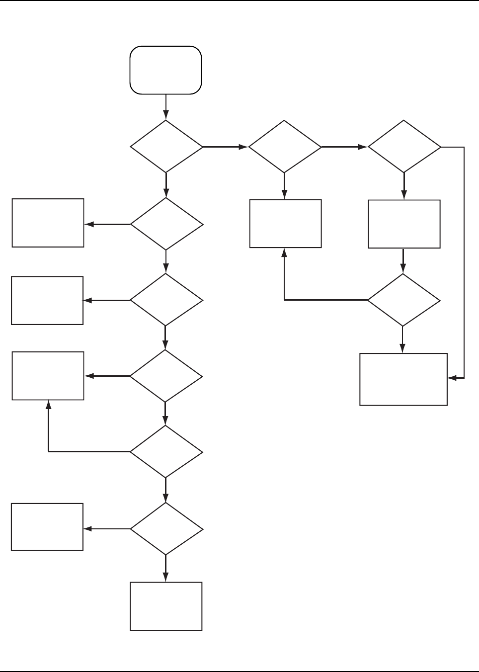
October 14, 2003 6881094C31-C
5-2 Troubleshooting Charts: Main Troubleshooting Flowchart
5.2 Main Troubleshooting Flowchart
MAEPF-27403-A
Start
Is TX
Deviation
OK?
Go to
TX RF
flowchart
Go to
VOCON
RX Audio
flowchart
Receive
Audio?
Good
SINAD?
Buttons
Functional?
End
Go to either
Display Failure or
Power-Up Failure
flowchart
See Button
Test flowchart
Error
Messages on
RSS?
Yes Ye s
Yes
Yes
Yes
Yes
Yes
Yes
Yes
No
No
No
No
No
No
No
No
No
Good
power-up
Self-Test?
Error
Message? Display
Model?
See Table 5-2:
Power-up Self-
Check Error
Codes
Is there
TX Power?
Go to
TX RF
flowchart
Use RSS to
display Error
Messages
6881094C31-C October 14, 2003
Troubleshooting Charts: Power-Up Failure 5-3
5.3 Power-Up Failure—Page 1
MAEPF-27389-C
Radio
Power-Up
Failure
Remove
R528 (VOCON)
Replace U301
(Flipper) and
place R528
back on board
Fixed?
Place R528
back on board
Probe
32.768 kHz
Clock at R316
Signal
Present?
Is
VOCON Board
NNTN4563, NNTN4819,
or NNTN4717
kit?
Signal may appear
for a very short period
of time (50 ms). Use
an oscilloscope with
trigger to capture signal.
Verify integrity
of C308 and
C309
Remove
Shield
SH101
Verify Standard
Bias in
Table 5-1
Standard
Bias OK?
Isolate and
Repair Problem
See DC Supply
Failure flowchart
No
No
No
No
Yes
Yes
Yes
Yes
1
2
October 14, 2003 6881094C31-C
5-4 Troubleshooting Charts: Power-Up Failure
Power-Up Failure—Page 2
MAEPF-27390-A
Investigate
Clock Buffer
Components and
Isolate Problem
This signal may
contain harmonics
and, therefore, may
not appear as a
perfect sinewave.
Signal may
appear for a very
short period of
time (50ms). Use
an oscilloscope
with trigger to
capture signal.
Refer Board to
Service Depot for
Reflash, Patriot,
SRAM, and
FLASH Analysis
Investigate
16.8 MHz
Reference
Oscillator
Probe
16.8 MHz
Signal at R452
Signal
greater than
600mV?
Signal
greater than
600mV?
Check
16.8 MHz
Signal at
C452
Replace
U301
Replace
Problem
Component
Components
OK?
Fixed?
End
Fixed?
Replace
Y301
No
No
No
No
No
Yes
Yes
Yes
Yes
Yes
1
2
Note: All components noted on this
chart are VOCON components.
6881094C31-C October 14, 2003
Troubleshooting Charts: DC Supply Failure 5-5
5.4 DC Supply Failure—Page 1
NOTE: Since the failure of a critical voltage supply might cause the radio to automatically power
down, supply voltages should first be probed with a multimeter. If all the board voltages
are absent, then the voltage test point should be retested using a rising-edge-triggered
oscilloscope. If the voltage is still absent, then another voltage should be tested using the
oscilloscope. If that voltage is present, then the original voltage supply in question is
defective and requires investigation of associated circuitry.
MAEPF-27391-A
Check Voltage
at pin 3 of
Q502
Replace
Q501
Check Voltage
at pin 2 of
Q502
Voltage
= 0V?
Replace
Q502
Check
Continuity of
Fuse F901
on transceiver
Voltage
= B+?
Voltage
= B+? Voltage
= B+?
Replace
Fuse
Replace Front
Cover Housing
Assembly
Fixed? End
Fuse OK?
Check Voltage
at pin 1 of
Q501
Check Battery
Connections for
Good Contact
Problem with
DC Distribution
Network
Check Voltage
at pin 5 of
Q501 (VOCON)
NoNo
No No
No
No
Yes
Yes Yes
Yes
Yes
1
Yes
October 14, 2003 6881094C31-C
5-6 Troubleshooting Charts: DC Supply Failure
DC Supply Failure—Page 2
MAEPF-27392-B
Check R763,
L703, C717,
and CR700
Check Voltage
at R560
Replace
Problem
Component
Voltage
= V2?*
Replace
U501
(GCAP II)
Check R502,
C506, L502,
and D503
Voltage
= 3.77V+/-5%?
Voltage
= 1.85V+/-5%? Components
OK?
ReFLASH
HOST C
Code
Fixed? End
Components
OK?
Check Voltage
at R501
Replace
Problem
Component
Check Voltage
at B502
(VOCON)
No
Yes
Yes
Yes
Yes
Yes
Yes
No
No
No
No
1
2
3
2
No
* per Standard Bias Table
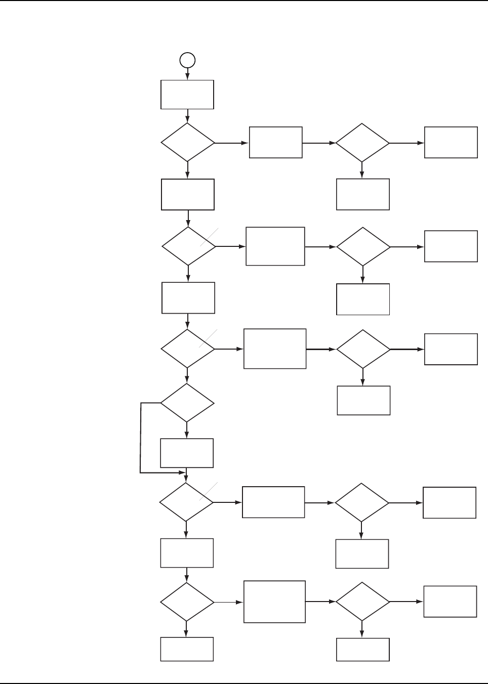
6881094C31-C October 14, 2003
Troubleshooting Charts: DC Supply Failure 5-7
DC Supply Failure—Page 3
MAEPF-27393-C
Voltage
= 5.0V+/-5%?
Check Voltage
at pin 5 of
U505 (VOCON)
No No
NoNo
No No
No
No
Yes
Yes
Yes
Yes Ye s
Yes
Yes
Yes
Yes
3
Check
700-800: E6, C15,
C16, C17, and D2
VHF: E6, C6,
C8, and D2
Voltage
= V2?* Components
OK?
Check R503,
D501, C509,
C510, and C508
Replace
Problem
Component
Replace
700-800: U505
VHF: U1
Replace
Problem
Component
Components
OK?
Check Voltage
at TP7
Check Voltage
at TP6
Replace
U2
Check Voltage
at TP5
Check
700-800: D1, E5,
C12, C13, and C14
VHF: E5, C3, C4,
C5, and D1
Check Voltage
at TP3
Replace
U3
End Replace
U1
Voltage
= 5.0V+/-5%?
Replace
Problem
Component
Voltage
= V2?*
No Is unit
VHF?
Components
OK?
Replace
Problem
Component
Check
700-800: D3, R704,
C19, and C20
VHF: E7, C9, C10,
C11, and D3
Components
OK?
No No
Yes Ye s
Replace
U5
Voltage
= V2?*
Replace
Problem
Component
Check
E8, C18, C19,
C20, and D4
Components
OK?
* per Standard Bias Table
* per Standard Bias Table
* per Standard Bias Table
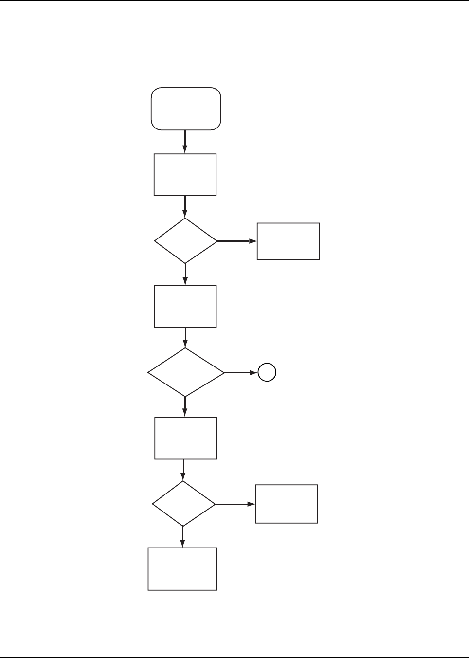
October 14, 2003 6881094C31-C
5-8 Troubleshooting Charts: Display Failure (NNTN4563, NNTN4819, & NNTN4717 VOCON Kits)
5.5 Display Failure (NNTN4563, NNTN4819, & NNTN4717 VOCON Kits)
Page 1
NOTE: The NNTN4563 VOCON board is compatible only with the 7285726C02 display module,
and the NNTN4819 VOCON board is compatible only with the 7285726C03 display
module.
MAEPF-27505-B
End
Replace
LCD Display
Check integrity
of B101
2.775 V<V<3.1 V?
No Display
Problem
Resolved?
No
No
Yes
Yes
Replace
B101
Verify V2
using
DC Supply Failure
flowchart
B101 OK? No
Yes
Check DC
on J301,
pins 17 and 18
1
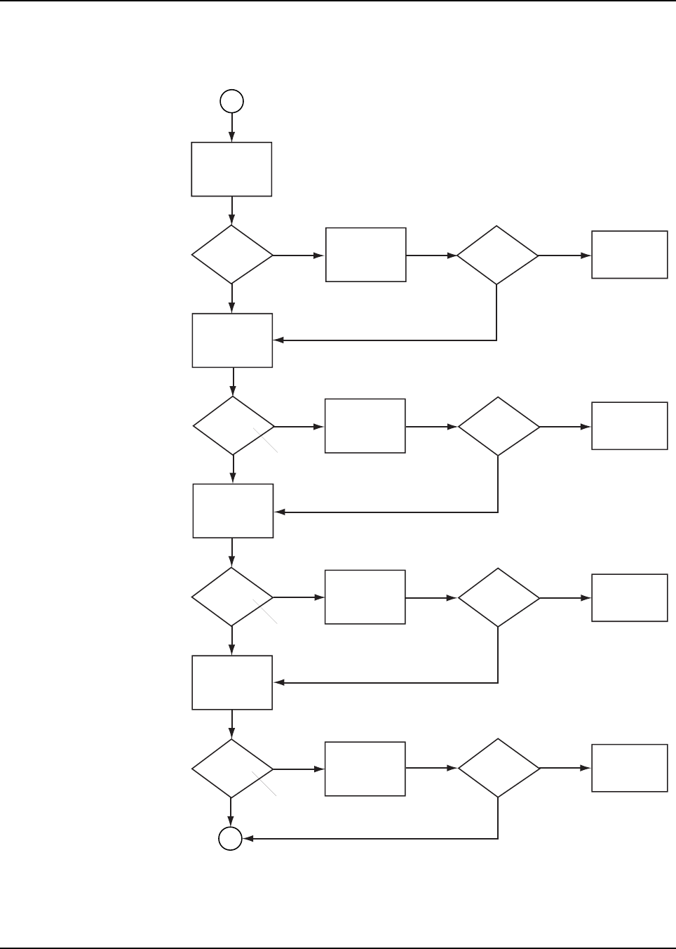
6881094C31-C October 14, 2003
Troubleshooting Charts: Display Failure (NNTN4563, NNTN4819, & NNTN4717 VOCON Kits) 5-9
Display Failure (NNTN4563, NNTN4819, & NNTN4717 VOCON Kits)
Page 2
MAEPF-27506-A
V = 0 V?
Check P_S*
at J301, pin 4
No Yes
YesNo
No Yes
Yes
No
No
No
No
No
Yes
Yes
Yes
Yes
1
Problem
Resolved?
Problem
Resolved?
Problem
Resolved?
Problem
Resolved?
Check
REG_SEL
at J301, pin 7
Check RESET
at J301, pin 6
Verify Signal
Path Integrity
and correct
Verify Signal
Path Integrity
and correct
Verify Signal
Path Integrity
and correct
Verify Signal
Path Integrity
and correct
Check CS at
J301, pin 5
3
V = V2?*
V = V2?* End
End
End
End
V = V2?*
* per Standard Bias Table
* per Standard Bias Table
* per Standard Bias Table
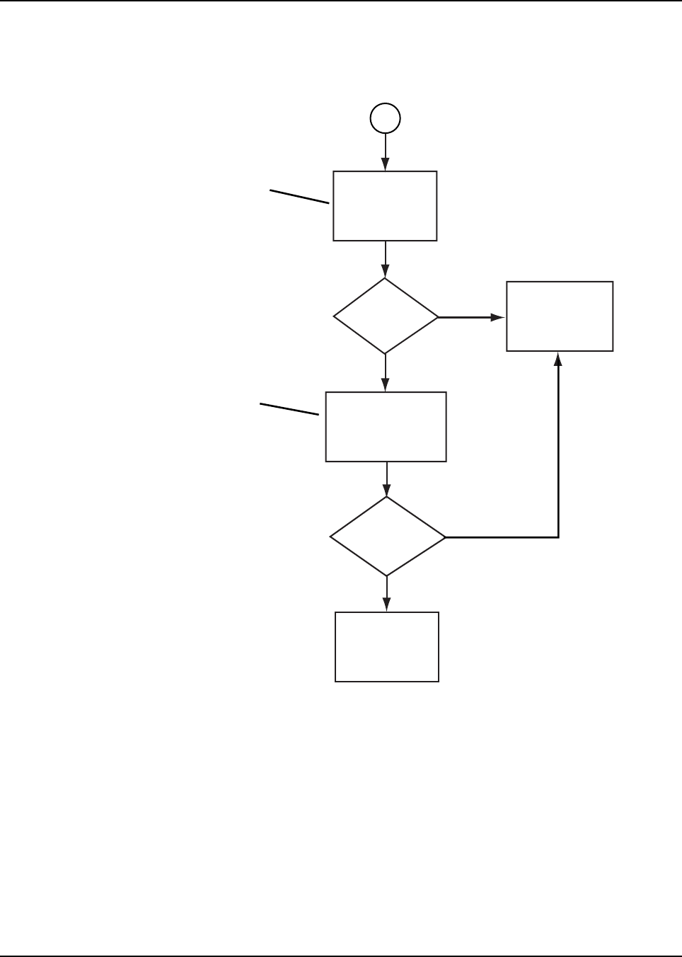
October 14, 2003 6881094C31-C
5-10 Troubleshooting Charts: Display Failure (NNTN4563, NNTN4819, & NNTN4717 VOCON Kits)
Display Failure (NNTN4563, NNTN4819, & NNTN4717 VOCON Kits)
Page 3
MAEPF-27507-A
Low-
Level Pulses
Present?
Check Active
Low Status on
both RESET
and CS
Use an oscilloscope to check for
a low-level (0V) pulse occurrence
during power-on initialization period.
Use an oscilloscope to check for
either a low-level (0V) pulse or
high-level (0-V2) occurrence during
power-on initialization period.
No
Yes
No
Yes
3
Signal
present
at appropriate
level?
Replace
Display
Check J301, pins
15 and 16 for
appropriate voltage
levels (0-V2)
Return radio to
service depot for
further analysis
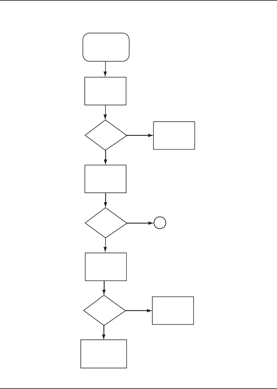
6881094C31-C October 14, 2003
Troubleshooting Charts: Display Failure (NTN9564) 5-11
5.6 Display Failure (NTN9564)—Page 1
NOTE: The NTN9564 VOCON board is compatible only with the 7285726C01 display module.
MAEPF-27404-O
End
Replace
LCD Display
Check integrity
of B102
1.8<V<1.95V?
No Display
Problem
Resolved?
No
No
Yes
Yes
Replace
B102
Verify VSW2
(1.85V) using
DC Supply Failure
flowchart
B102 OK? No
Yes
Check DC on
J301, pin 17
1
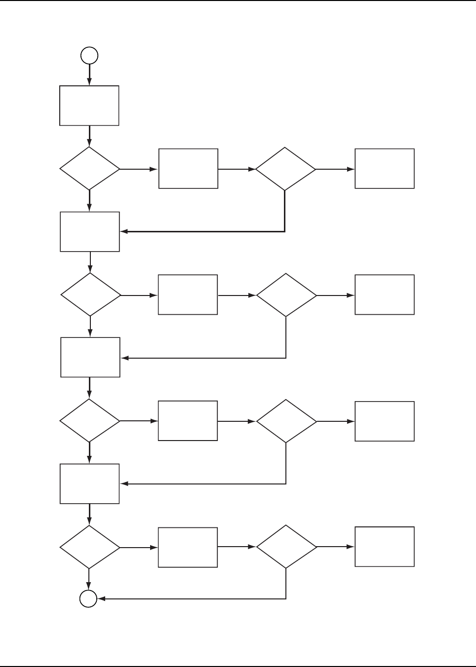
October 14, 2003 6881094C31-C
5-12 Troubleshooting Charts: Display Failure (NTN9564)
Display Failure (NTN9564)—Page 2
MAEPF-27405-O
V = 1.85V?
Check P_S*
at J301, pin 4
No Yes
YesNo
No Yes
Yes
No
No
No
No
No
Yes
Yes
Yes
Yes
1
V = 1.85V?
Problem
Resolved?
Problem
Resolved?
Problem
Resolved?
Problem
Resolved?
Check
REG_SEL
at J301, pin 7
Check RESET
at J301, pin 6
Verify Signal
Path Integrity
and correct
Verify Signal
Path Integrity
and correct
Verify Signal
Path Integrity
and correct
Verify Signal
Path Integrity
and correct
Check CS at
J301, pin 5
3
V = 1.85V?
V = 1.85V? End
End
End
End
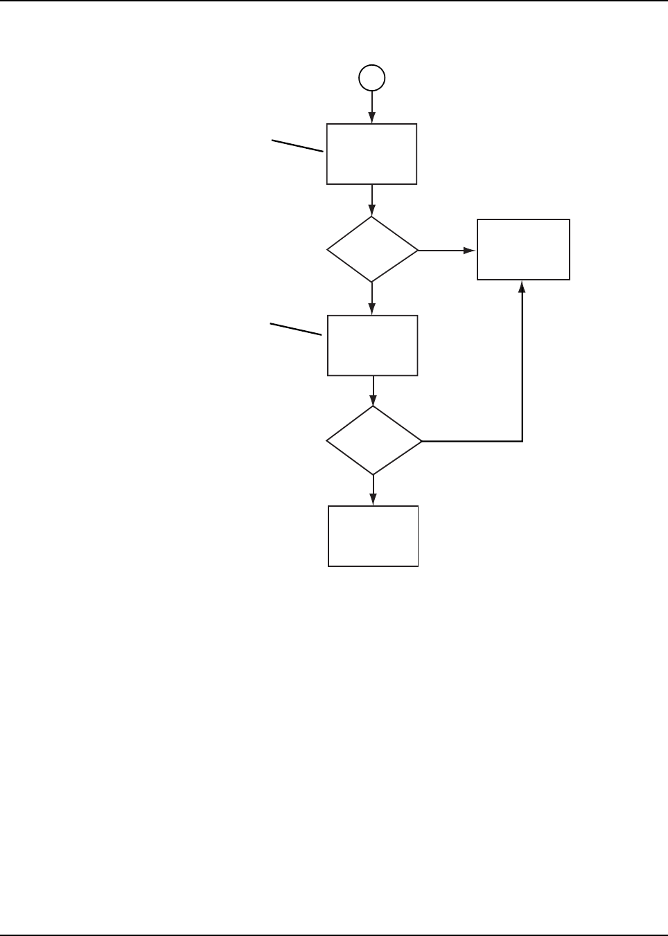
6881094C31-C October 14, 2003
Troubleshooting Charts: Display Failure (NTN9564) 5-13
Display Failure (NTN9564)—Page 3
MAEPF-27406-O
Low-
Level Pulses
Present?
Check Active
Low Status on
both RESET
and CS
Use an oscilloscope to check for
a low-level (0V) pulse occurrence
during power-on initialization period.
Use an oscilloscope to check for
either a low-level (0V) pulse or
high-level (1.85V) occurrence during
power-on initialization period.
No
Yes
No
Yes
3
Signal
present
at appropriate
level?
Replace
Display
Check D0-D7
for appropriate
voltage levels
Return radio to
service depot for
further analysis
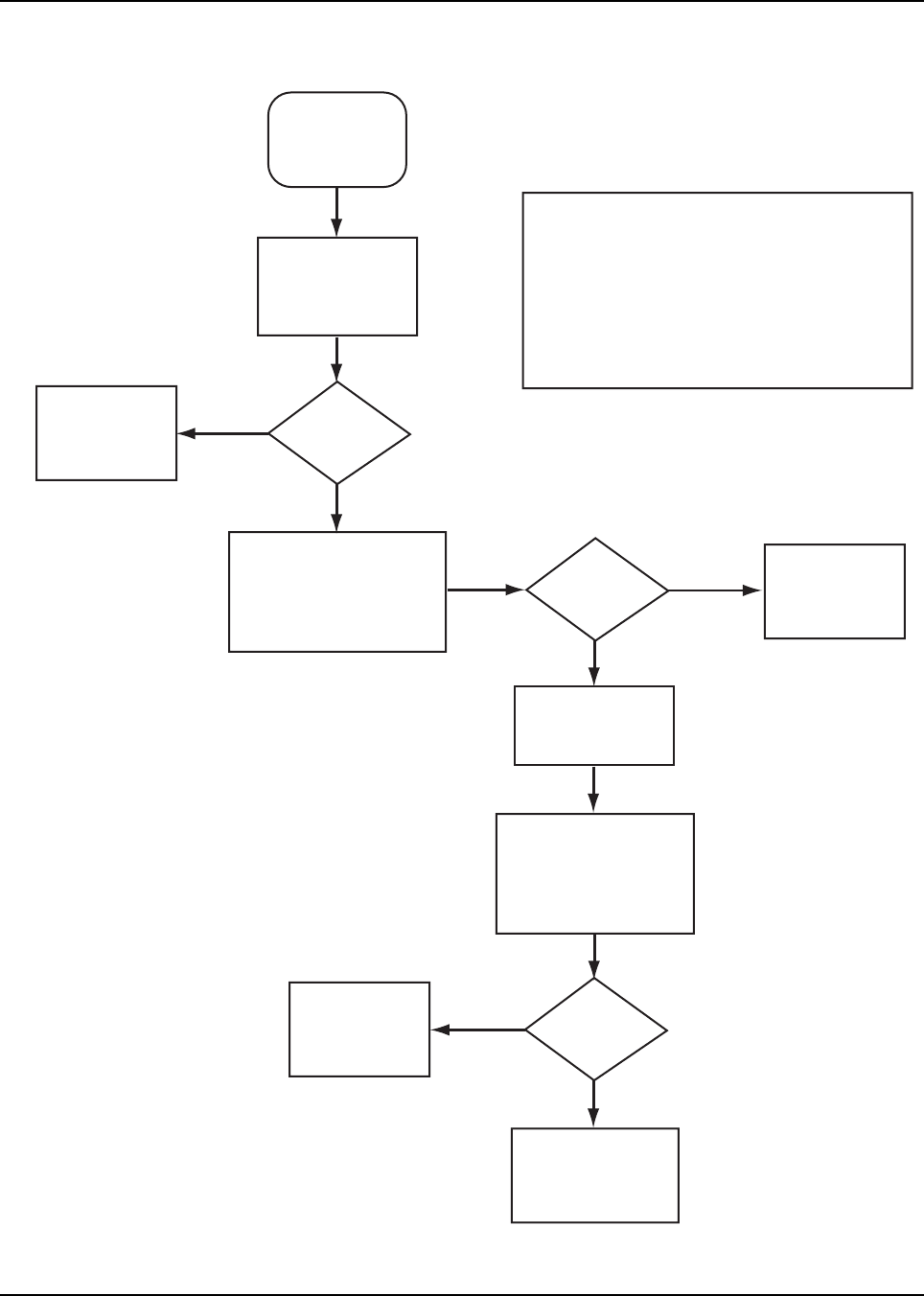
October 14, 2003 6881094C31-C
5-14 Troubleshooting Charts: Volume Set Error
5.7 Volume Set Error
MAEPF-27401-A
No
No
No
Yes
Yes
Yes
Volume
Set Error
Using a voltmeter,
measure voltage at
U507 pin 1, when volume
knob is all the way on.
The value should be V2*
Voltage
Functional? Replace
U501
Verify connections
and control top/PTT
flex connections
Volume
check OK?
Refer to
VOCON RX
Audio flowchart
Verify operation
of volume knob
using Button Test
flowchart
Replace
U507
Volume
pot OK?
Replace Front
Cover Housing
Assembly
This chart relates to a failure in the volume
set knob. Basic failure modes are as follows:
1) Failure in control top/PTT flex circuit
2) Bad connection
3) Defective volume control potentiometer
4) Defective A/D port in GCAP II
5) Problem in receive audio circuit
Synopsis
Measure voltage from
R526 to GND while
moving volume knob
from min to max. Max
volume is 2.50V
* per Standard Bias Table
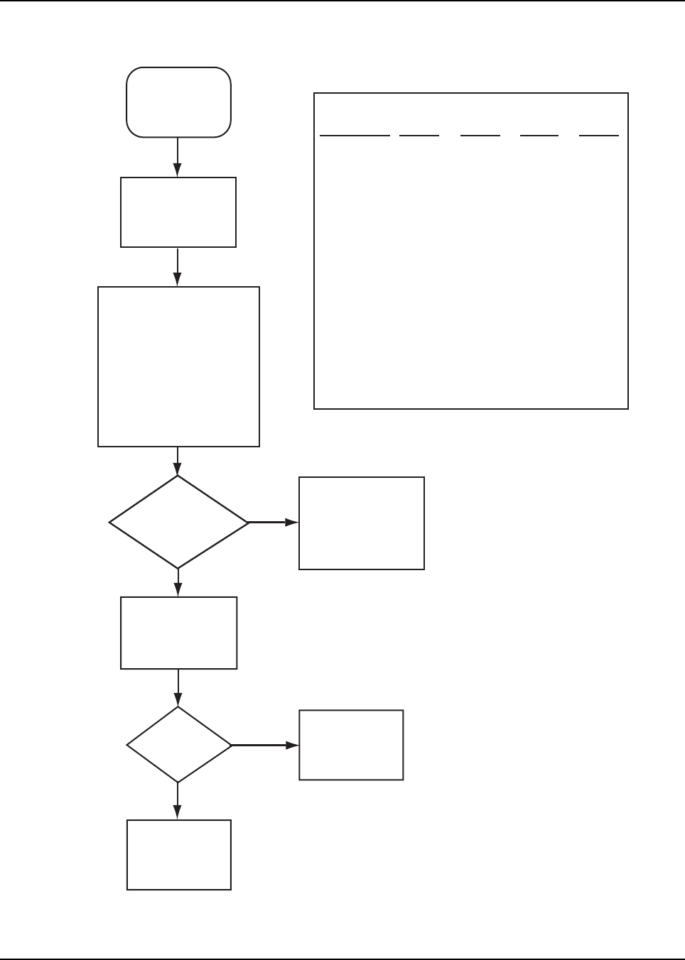
6881094C31-C October 14, 2003
Troubleshooting Charts: Channel/Zone Select Error 5-15
5.8 Channel/Zone Select Error
MAEPF-27402-O
Replace Front
Cover Housing
Assembly
Repair flex or
connections as
needed
U1
checks
good?
Verify operation
of zone knob
using Button Test
flowchart
Signals
check good at U1
on the controls
flex assy.?
Verify codeplug
programming with
RSS. If codeplug
checks OK, then
replace U1.
By studying the
adjacent table against
the channel numbers
that have errors, one
signal may be determined
to be in error. Verify
logic levels at R235,
R236, R239, and R241
for each channel.
Channel
Select Error
No
No
Yes
Yes
Verify similar
operation directly
at U1 on controls
flex assembly
RTA3
(R241) RTA2
(R239)
RTA1
(R236) RTA0
(R235)
Channel
Probe Point
1
1
1
1
1
1
1
1
0
0
0
0
0
0
0
0
1
1
1
1
0
0
0
0
1
1
1
1
0
0
0
0
1
1
0
0
1
1
0
0
1
1
0
0
1
1
0
0
1
0
1
0
1
0
1
0
1
0
1
0
1
0
1
0
1
2
3
4
5
6
7
8
9
10
11
12
13
14
15
16
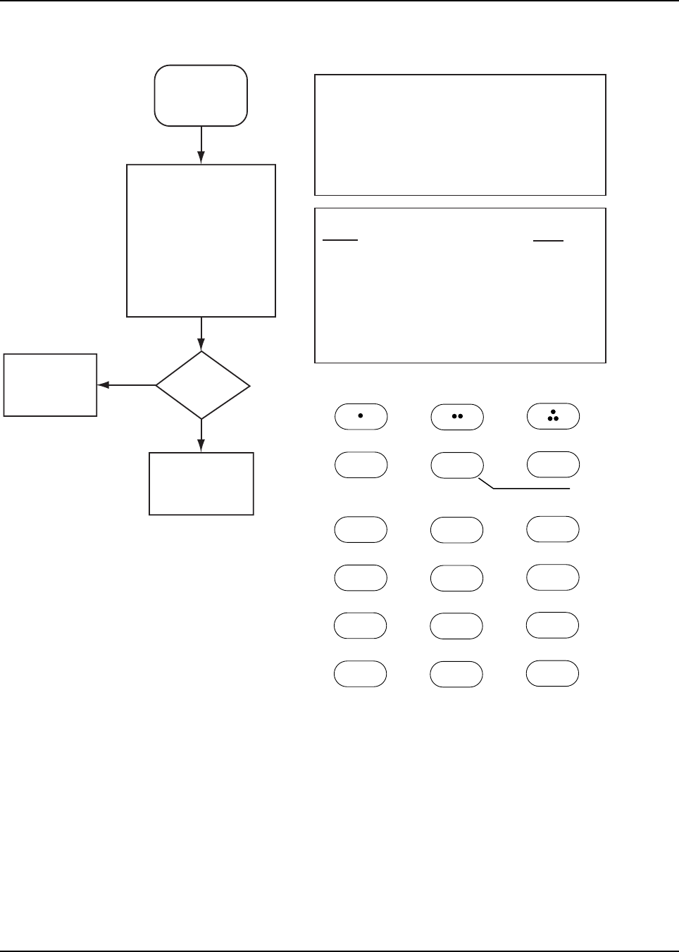
October 14, 2003 6881094C31-C
5-16 Troubleshooting Charts: Button Test
5.9 Button Test
MAEPF-27399-O
End Keys
correct?
Check signal
path integrity of
button in question
Button Test
Place radio in Test Mode.
Press Top Side Button
(Monitor) so display reads
CH TEST. This places the
radio in button test mode.
Then, press the orange
(Emergency) Top Button
to verify codes displayed
as shown in the Button
Table at right
No
Yes
This chart relates to a failure in the button functions
Basic Failure modes are as follows:
1) Failure in control top/PTT or keypad flex assembly
2) Bad Connection
3) Defective Switches or pads
4) Defective A/D port in GCAP II
Synopsis
Button Table
Button
PTT
Top Button (Emergency)
Side Button 1 (Monitor)
Side Button 2
Side Button 3
Channel Select (Frequency)
Volume Control Knob
Zone Select
Code
1/ 0-1
3/ 0-1
96/ 0-1
97/ 0-1
98/ 0-1
4/ 0-15
0/ 0-244
65/ 0-2
128/1 130/1
135/1
136/1
Home Alpha
129/1 134/1
132/1
131/1 133/1
53/1
5JKL
52/1
4GHI
54/1
6MNO
50/1
2ABC
49/1
1
51/1
3DEF
48/1
0
58/1
*
59/1
#
56/1
8TUV
55/1
7PRS
57/1
9XYZ
Navigation
Button
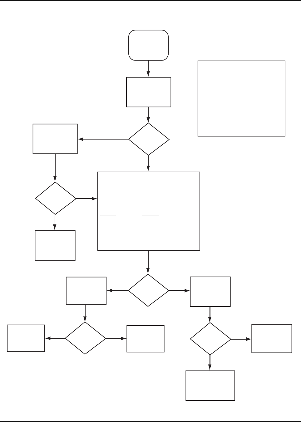
6881094C31-C October 14, 2003
Troubleshooting Charts: Top/Side Button Test 5-17
5.10 Top/Side Button Test
MAEPF-27400-O
Use RSS
to enable
button
Replace
U504
Replace Front
Cover Housing
Assembly
Verify connections
and control top/PTT
flex circuit and
repair as necessary
Using RSS,
verify problem
button is enabled
for function
Levels
correct?
Verify physical
operation of
buttons
Buttons
OK?
Button
check OK?
Buttons
Enabled?
Using a voltmeter, measure the voltage at
U504 pin 3 while depressing the following
buttons: Emergency, Side Button 1, Side
Button 2, and Side Button 3.
The probe points are as follows:
Button
Emergency
Top Side
Middle Side
Bottom Side
None Pressed
Voltage
0.18V
1.40V
1.70V
2.00V
2.50V
Top/Side
Button Test
Synopsis
This chart relates to a failure in
reading the buttons: Emergency,
Side Button 1, Side Button 2, or
Side Button 3.
Basic failure modes are as follows:
1) Failure in controls flex circuit
2) Bad connection
3) Defective Switch
4) Defective A/D port in GCAP II
Verify operation
of zone knob
using Button Test
flowchart
No
No
Yes
Yes
No
Replace
U501
Problem
fixed? End
No Yes No
Yes
Yes
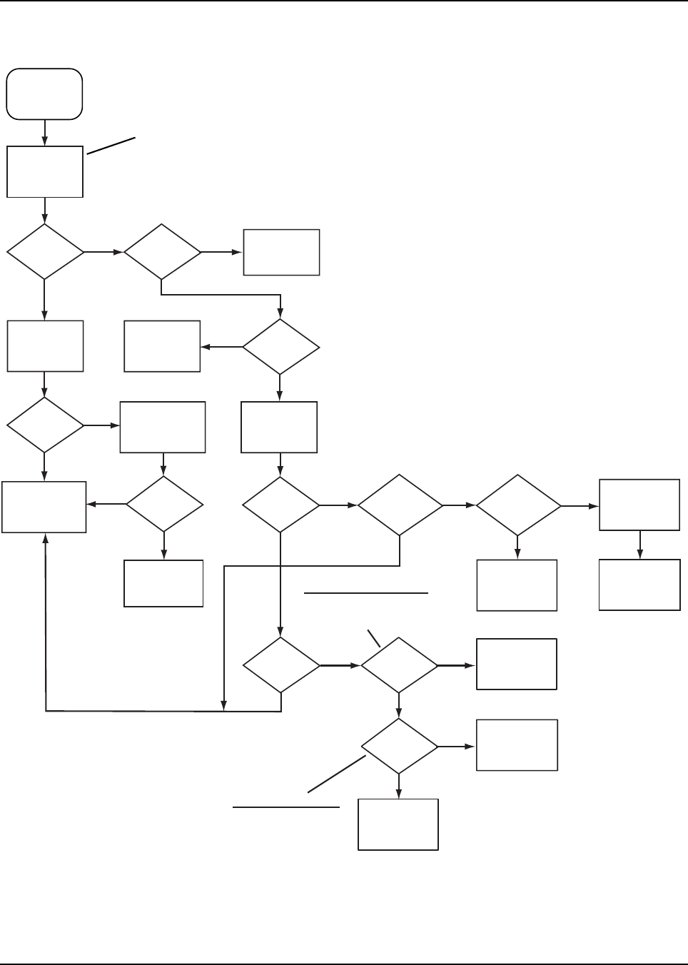
October 14, 2003 6881094C31-C
5-18 Troubleshooting Charts: VCO TX/RX Unlock
5.11 VCO TX/RX Unlock
MAEPF-27398-A
VCO TX/RX
unlock
<0.6Vdc
>11.0Vdc or
drifting?
3V at TP5?
Yes
Yes
Yes
Yes
Yes
Yes
No
No
No No
No
Yes
Yes Ye s
Frequency
detected?
VCO locked?
No
Yes
No
5V at TP3?
Check
VOCON board
Check parts
around BJT. If
OK, replace BJT
Check control
voltage at
TP243
Check parts
around U1. If
OK, replace U2
Aux.
line 1 (2,4)
is high?
Aux. line
3 high for TX
or low for RX
(VHF)?
Is unit
VHF?
No
No
FET
drain voltage
0V?
Check parts
around FET. If
OK, replace FET
No
BJT
emitter voltage
>1.2V?
Check parts
around U300. If
OK, replace U300
Yes
Check parts
around U302.
If OK, replace
Q302
No
Is pin
19 of VCOBIC
low for RX and
4.5 for TX?
Remove
VCO buffer
shield (SH302)
Check parts
around Q301. If
OK, replace Q301
Check parts
around U2. If
OK, replace U2
Remove
VCO shield
Check parts
around U202. If
OK, replace U202
"Sniff"
frequency near
VCO shield
Check if VCO
is locked using
spectrum analyzer
Sniff: Using an inductive field probe
as an antenna to measure
frequency. Place the probe
approximately 1/2 inch away
from components to be sniffed.
Q302 VC01
Q306 VC02
Q309 VC03
Field Effect Transistor (FET)
Q301 VC01
Q303 VC02
Q308 VC03
Bi-polar Transistor (BJT)
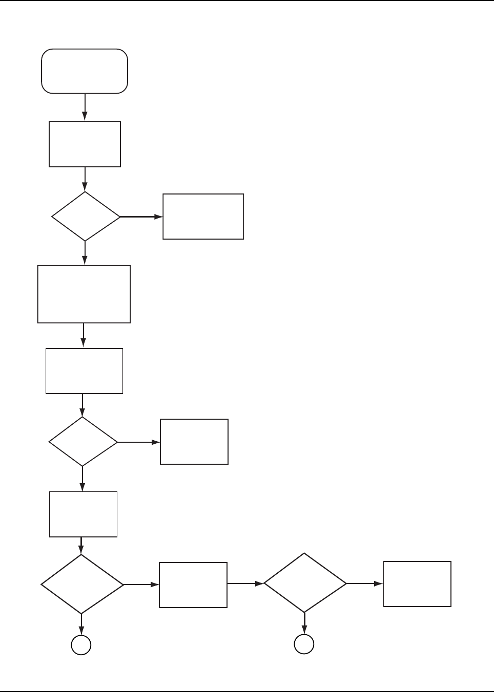
6881094C31-C October 14, 2003
Troubleshooting Charts: VOCON TX Audio 5-19
5.12 VOCON TX Audio—Page 1
MAEPF-27396-O
Inject a 200 mV
rms 1.0 kHz tone
to the test box
Audio In port
Repair connections
and/or replace flex
and microphone
Connections
OK?
Problem
with Mic path
components?
No Problem
found.
End
Replace
appropriate
component
Is FM
deviation approx.
3.0 kHz?
Connect an
RLN4460A audio
test box (or equivalent)
to the radio side
connector
Radio has no
Transmitter Deviation
(VOCON Evaluation)
Inspect
Microphone and
Flex Connector
Yes
No
Yes
Yes
No
12
No
Probe Voltage
at U509, pin 5
Verify Integrity
of Mic path up
to U509
Is
1 kHz Signal
present at approx.
14 mV rms?
No
Yes
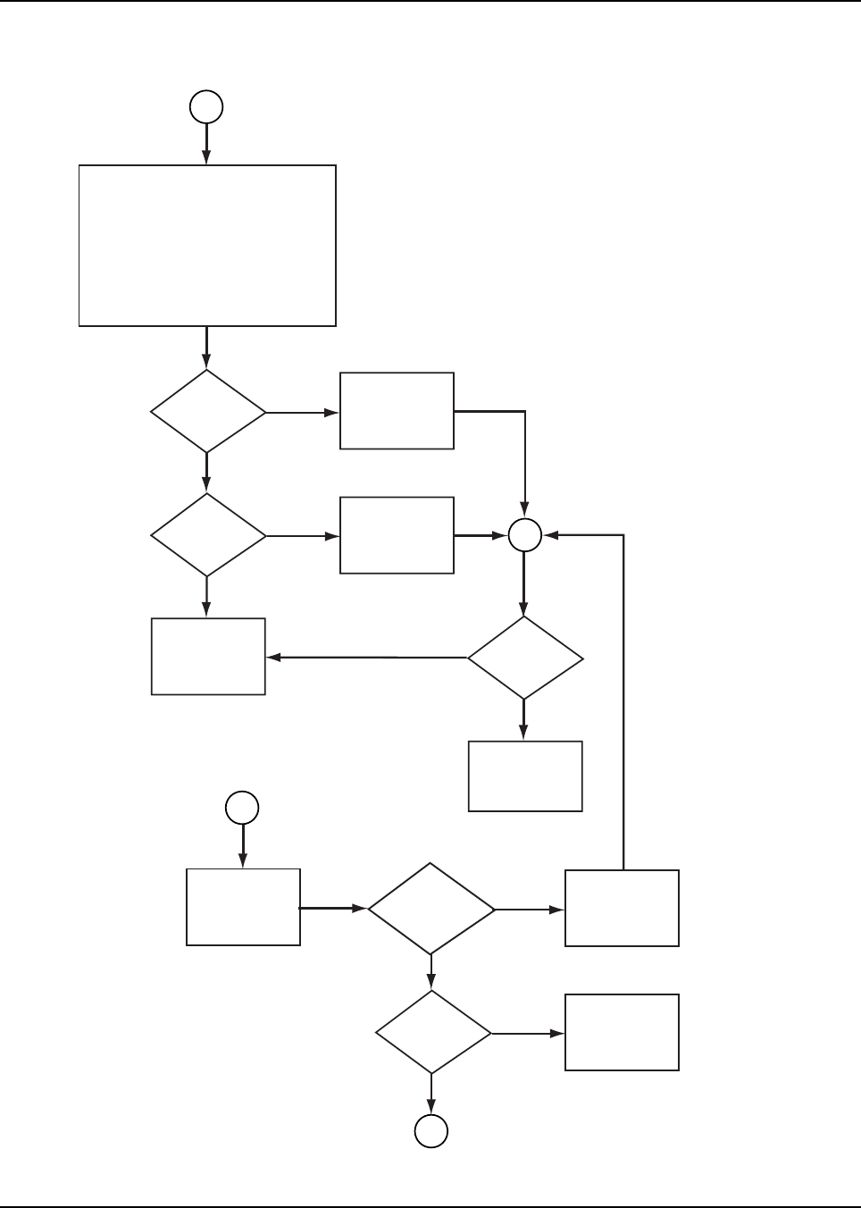
October 14, 2003 6881094C31-C
5-20 Troubleshooting Charts: VOCON TX Audio
VOCON TX Audio—Page 2
MAEPF-27397-A
Replace U501
(GCAP II)
Replace
U509
(EEPOT)
Go to
TX RF
flowchart
Replace U301*
(Flipper ASIC)
Clock
and Frame Sync
present?
Data
present at TX
test point?
Use an oscilloscope to check the
SSI audio signals from the GCAP
(U703). The following test points
are used for data collection:
DCLK: 520 kHz Square Wave Clock*
TX: Audio Data Words
SYNC: 8 kHz Frame Sync Pulse
No
Yes
Yes
End
Problem
Resolved?
Yes
1
2
1
No
No
End
Replace
U501
(GCAP II)
Is
1 kHz signal
present at about
14 mV
rms?
Problem
Solved?
No
Yes
No
Yes
256 kHz Square Wave Clock** * on NTN9564, NNTN4563 & NNTN4819 VOCON boards
** on NNTN4717 VOCON board
* on NTN9564, NNTN4563 & NNTN4819 VOCON boards
** on NNTN4717 VOCON board
Replace U401**
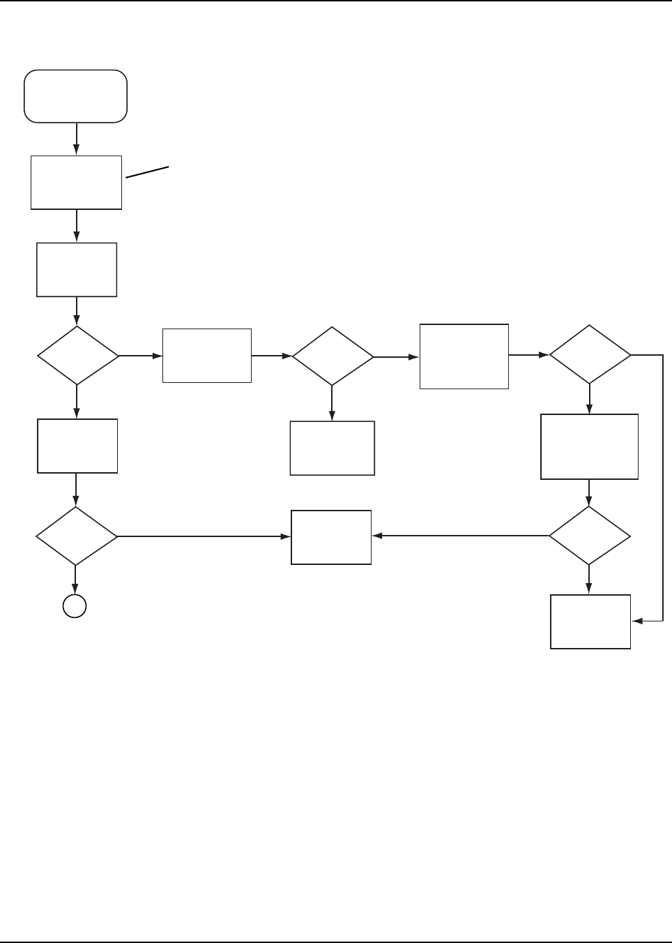
6881094C31-C October 14, 2003
Troubleshooting Charts: VOCON RX Audio 5-21
5.13 VOCON RX Audio—Page 1
MAEPF-27394-A
* on NTN9564, NNTN4563 & NNTN4819 VOCON boards
** on NNTN4717 VOCON board
Probe R406 for
Frame Sync Signal,
Compare with
RX SAP waveform,
Trace 1
Frame
Sync
Present?
Replace U301*
(FLIPPER)
Probe R403 for
Data, Compare
with RX SAP
waveform, Trace 2
Signal
Present?
THD <3%?
Clock
Present?
Probe R405
for Clock Signal,
Compare with
RX SAP
waveform, Trace 3
Go to
RX RF
flowchart
Data
Present?
Check
Distortion of
Signal at C533
Replace U501
(GCAP II)
Check Preamp
Input Signal at
C533
NoNo
No
No
No
Yes
Yes
Yes
Yes
1
Yes
Bad SINAD
Bad 20db Quieting
No Recovered Audio
Inject Standard
Input into Antenna
Connector
A standard input is an
RF signal with a 1 kHz
tone modulated with 3 kHz
deviation in a 25 kHz channel.
Replace U401**
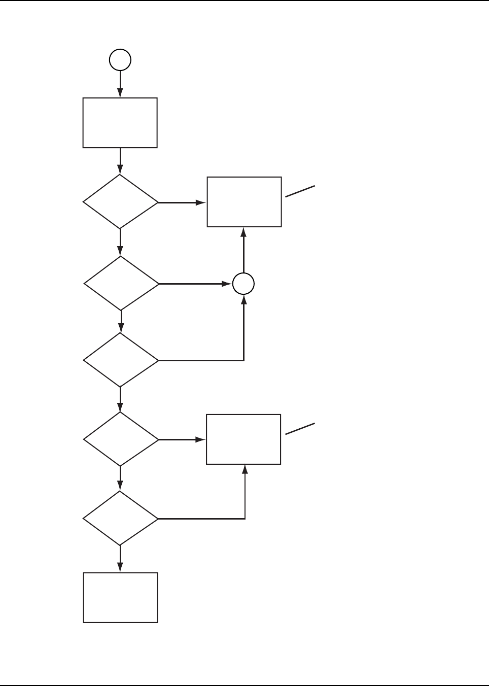
October 14, 2003 6881094C31-C
5-22 Troubleshooting Charts: VOCON RX Audio
VOCON RX Audio—Page 2
MAEPF-27395-O
Make sure that you look at
all solder contacts. Check
resistors and capacitors
associated with this check. If
all look fine, then replace U502.
Make sure that you look at
all solder contacts. Check
resistors and capacitors
associated with this check. If
all look fine, then replace U503.
Signal
Present?
Check Preamp
Output Signal
at C530
No
No
No
No
No
Yes
Yes
Yes
Yes
Yes
1
Preamp Gain
= 2.8 V/V?
PA Gain
= 11.2 V/V?
Distortion
>3%?
Check Preamp
U502 and its
associated
components
Check Flex
Connector
Distortion
>3%?
Check Audio PA
U503 and its
Components
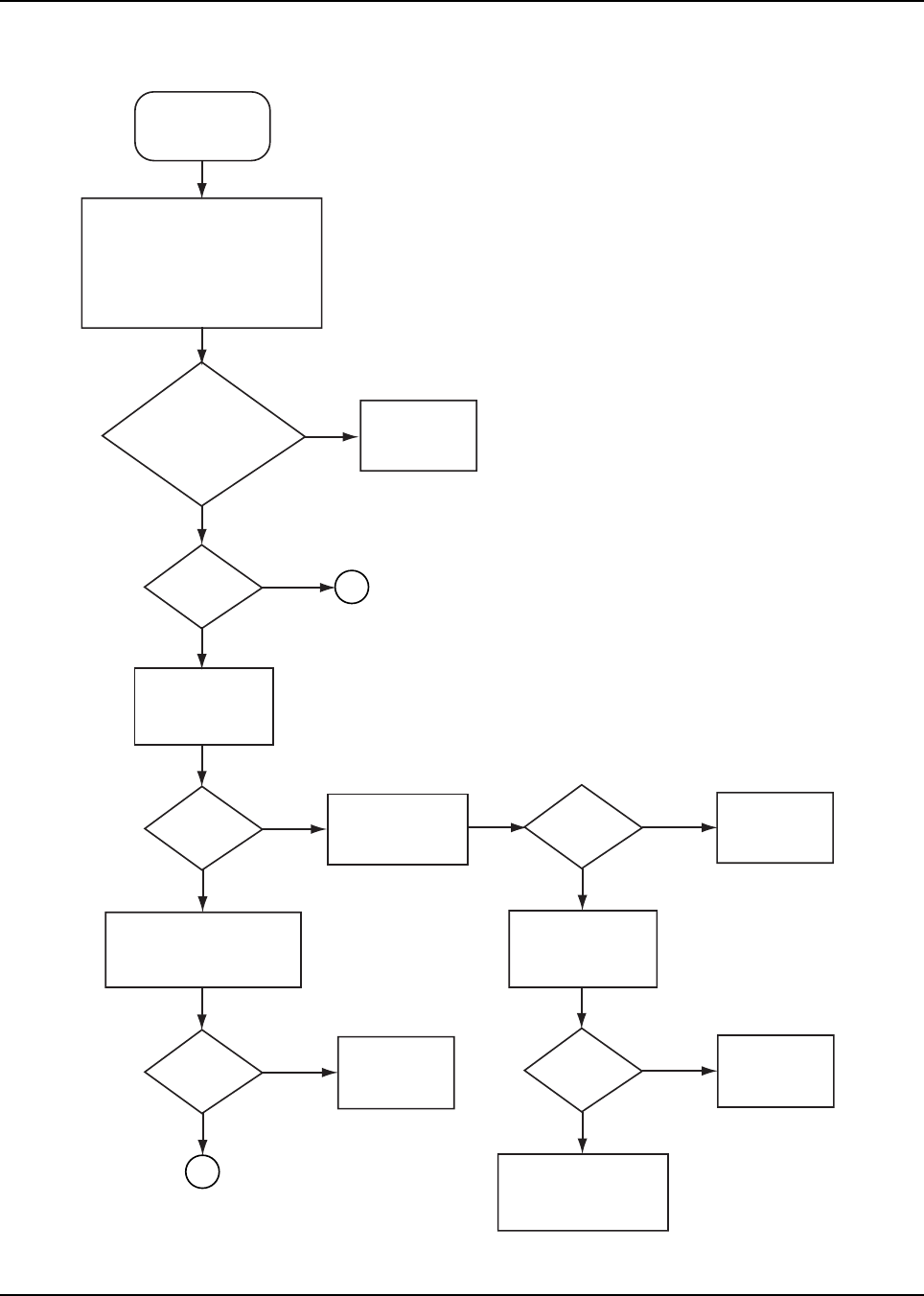
6881094C31-C October 14, 2003
Troubleshooting Charts: RX RF 5-23
5.14 RX RF—Page 1
Frequency OK?
VHF: 44.85 MHz
UHF: 73.35 MHz
700-800: 109.65 MHz
Inject a standard FM test signal
into the antenna port. Use CPS to
ensure that attenuator feature is
disabled. Use a spectrum analyzer
and high-impedance RF probe to
measure the IF signal at TP12
(700-800) or TP15 (VHF) on side 2
No
No
Yes
Yes
Poor RX
sensitivity or
no RX audio
Check
RXLO
Replace
bad part
Remove cable
assembly, measure
insertion loss
Visual
inspection
OK?
No
Yes
Bad antenna connector.
Replace chassis
(connector is not
serviceable)
Loss
< 0.2 db? Replace
cable assembly
No
Yes
Inspect coaxial
antenna connector
and cable assembly
Measure RF
input level
at TP02
Measure RF levels at TP02
and TP13 (UHF & 700-800)
or TP401 (VHF),
compute SW_FL loss
RF level
about
-47 dBm?
No
Yes
SW_FL
loss < 2 dB? Check
SW_FL
Yes
No
IF
level about
-38 dBm? 1
2
3 kHz FM deviation,
1 kHz rate, -47 dBm
MAEPF-27470-B
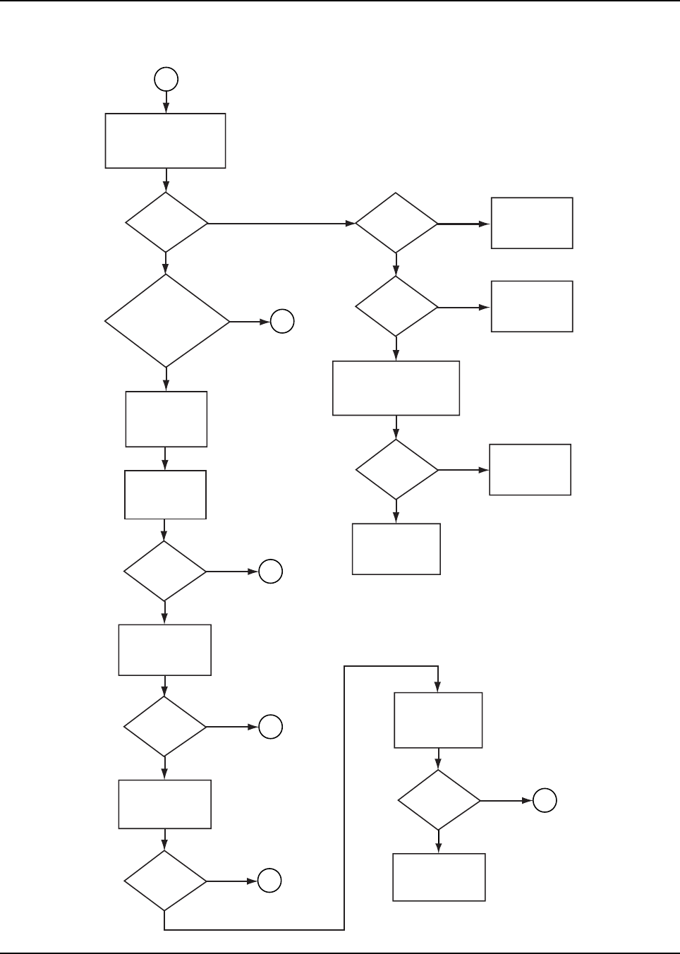
October 14, 2003 6881094C31-C
5-24 Troubleshooting Charts: RX RF
RX RF—Page 2
Q501-c
= 5.0 Vdc? No
No
No
Yes
Yes
Yes
Repair
Defects
Visual
examination
OK?
Check Voltage
Regulator U1
Q501-e
= 3.7 Vdc?
No
Yes
Replace
Q501
Replace
Q502
Remove SH501
(UHF & 700-800)
or SH502 (VHF), inspect
2nd LO VCO
Signal
Present?
Measure 2nd LO at
TP501 (UHF & 700-800)
or TP18 (VHF)
on PCB side 2
No
No
Yes
Yes
LO Freq.
OK?
VHF: 42.6 MHz
UHF: 71.1 MHz
700-800:
107.4 MHz
Measure
RXCK, P1-5
RXFS, P1-6
RXDO, P1-12
Observe
0 to 3 Vdc
digital signals
Measure
bit clock rate
(Fbit) at RXCK
Levels
OK?
1
3
5
No
Yes
RXFS = 20 kHz
sync pulse
Fbit =
1.2 MHz? 4
No
Yes
No
Yes
RXFS
OK?
RXDO = 24-bit I,
24-bit Q, 8-bit
AGC. AGC varies
with RF level
Go to
VOCON RX
AUDIO flowchart
RXDO
OK?
5
5
2nd LO, 700-800: 107.4 MHz, VHF: 42.6 MHz, about 356 mVpp
2nd LO DC bias
MAEPF-27471-B
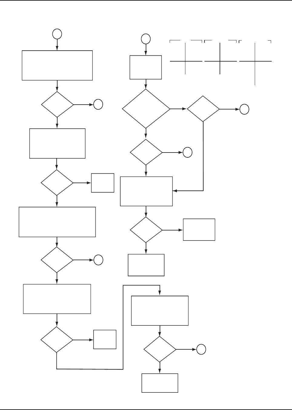
6881094C31-C October 14, 2003
Troubleshooting Charts: RX RF 5-25
RX RF—Page 3
TP502
= 0 Vdc?
No
No
Yes
Yes
Repair
defects
Measure RF levels at first preselector
filter and compute filter loss.
VHF: TP401, TP9
UHF: TP13, U401-3
700-800: TP13, D401-3
No
Yes
Loss < 3 db?
Measure RF levels at LNA
and compute LNA gain.
VHF: TP9, TP12
UHF: U401-1, TP402
700-800: D401-3, TP402
Measure RF levels at second preselector
filter and compute filter loss.
VHF: TP12, TP451
UHF: TP402, TP403
700-800: TP402, TP403
Gain
about
+12 dB?
2
6
No
Yes
Measure RF and IF level at mixer
and compute mixer conversion gain.
VHF: TP451, TP15
UHF: TP403, TP404
700-800: TP403, TP404
Loss
< 3 dB? 8
No
Yes
Measure
control voltage
at TP502
No
Yes
Fvco
too low?
VHF: < 42.6 MHz
UHF: < 71.1 MHz
700-800:
< 107.4 MHz
Remove Abacus shield and
inspect second LO VCO.
VHF: SH502
UHF: SH501
700-800: SH501
TP502
= 5 Vdc?
3
5
5
No
Yes
Replace
Varactor D550
Check
LNA
Check
mixer
Visual
examination
OK?
No
Yes
Measure IF level at XTAL filter
and compute XTAL filter loss.
VHF: TP15, TP455
UHF: TP404, TP12
700-800: TP404, TP12
Mixer
gain about
4 dB? No
Yes
No problem
found
Loss
< 3 dB? 7
MAEPF-27472-B
TP502
(Vdc) TP501
(MHz)
Fvco
1.7
3.7 71.1
75.6
UHF R1
TP502
(Vdc) TP18
(MHz)
Fvco
1.40
3.20 42.6
47.1
TP502
(Vdc) TP501
(MHz)
Fvco
0.00
1.85
4.30
5.00
101.0
107.4
111.9
113.0
700-800 MHz
VHF
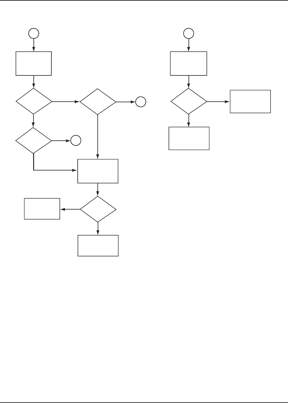
October 14, 2003 6881094C31-C
5-26 Troubleshooting Charts: RX RF
RX RF—Page 4
Yes
Fbit
< 1.2 MHz?
Measure
tuning voltage
(Vt) at R512
No
No
No
Yes
Yes
Vt= 3 Vdc?
Repair
defects
Replace
Varactor D501
Replace
Abacus
U500
Repair
defects
Visual
examination
OK?
4
Visual
examination
OK?
Remove SH501,
inspect
components
No
Yes
5
5
No
Yes
Remove SH501,
inspect clock
oscillator circuit at
U500-19, 20
Vt = 0 Vdc? 5
Clock
synthesizer
MAEPF-27473-O
6881094C31-C October 14, 2003
Troubleshooting Charts: RX RF 5-27
RX RF—Page 5
dac1 = dac2?
Measure prselector filter
tuning voltage dac1 and dac2.
VHF: None, TP29
UHF: TP401, TP405
700-800: TP401, TP405
No
Yes
Is
unit
VHF?
No
Yes
Replace IF filter.
VHF: FL451
UHF: FL490
700-800: FL403
Repair
defects
68
Visual
inspection
OK?
Remove IF filter shield. Check IF
filter and LC matching networks.
VHF: SH451
UHF: SH403
700-800: SH403
No
Yes
VHF/UHF: Check discrete
preselector filters.
700-800: Replace FL401
or FL402.
Replace
PCIC
Dac
voltages
OK?
Tune the radio across several
channels. Measure dac2,
proportional to frequency.
No
Yes
7
Replace
PCIC
MAEPF-27474-B
VHF
UHF
700-800
136
174
380
470
770
869
1.3
2.4
0.5
2.9
1.5
3.5
Band F (MHz) dac2 (Vdc)
October 14, 2003 6881094C31-C
5-28 Troubleshooting Charts: TX RF (VHF)
5.15 TX RF (VHF)—Page 1
TX
power OK?
Place XCVR and VOCON
into the analysis fixture.
Key up. Measure RF
power at antenna port
Yes
No
Yes
No
No or low
TX power
Check
FGU
Frequency
OK?
No
Yes
Check
FGU
Level
about
-3 dBm?
Check coaxial
connector and
cable assembly
Measure RF level
at Q107 pin 2
Use a spectrum analyzer
and high-impedance RF
probe. Measure TXRF
at C016
Level about
+15 dBm? No
No
Yes
Yes
Level about
0 dBm?
No
Measure
drain of
Q104
Measure RF
level
at C147
Yes
Remove SH701
and check for
parts off pad
Check bias of Q101,
Q103, and Q106.
Replace bad
transistors
Is voltage
5 V?
1
2
MAEPF-27635-O

6881094C31-C October 14, 2003
Troubleshooting Charts: TX RF (VHF) 5-29
TX RF (VHF)—Page 2
MAEPF-27420-B
RAWB+
about
7.2 Vdc?
Measure
RAWB+
at Q107-drain
No
No
No
Yes
Yes
Yes
Check
continuity
V.gate
about 2 to
3 Vdc?
Check
continuity
DC bias is OK,
control is OK,
RFIN is OK,
PA has low gain
Replace
Q107
No
Yes Measure RF
level at
pin 6 of Q107
Is
unit
VHF?
No Yes Remove SH101
and check for
parts off pad
Level
about
+35 dBm?
Replace U102.
For VHF, check under
SH101. if all parts soldered,
replace U102.
Measure
gate bias
at L108
RAWB+
about
7.2 Vdc?
Measure
RAWB+
at U102-6
No
No
Yes
Yes
TX7V
about
7.2 Vdc?
Check
continuity
Measure
Vgate at TP111,
normally 4 to
5.5 Vdc
Measure
TX7V at
U102-14
DC bias is OK,
control is OK,
RFIN is OK, driver
has low gain
Vgate
> 4 Vdc?
2
1
3
4
October 14, 2003 6881094C31-C
5-30 Troubleshooting Charts: TX RF (VHF)
TX RF (VHF)—Page 3
INT > 5 Vdc?
Vgate at TP111
is low (< 4 Vdc)
Measure INT
at TP104
Yes
No
No
Yes
Yes
No
Replace
Q108
INT is low.
Measure VLIM
at TP119
PCIC is
programmed.
Measure TEMP
at R130
Bad PCIC
Replace U104
VLIM
about 2 to
3 Vdc?
No
Yes
Measure
RFIN at
TP101
TEMP
< 1.0 Vdc at
25C?
RFIN is low, INT
is low, bad PCIC,
replace U104
TP101
< 0.5 Vdc?
Low output power,
RFIN is high, check
RF detectors and
op amp U106.
Repair defects
Repair temperature
sensor circuit
(U103, Q109,
R130)
4
4
TXINH
< 1 Vdc?
TX7V is low.
Measure TXINH
at P1-19, Q101-b
No
No
Yes
Yes
RXH
< 1 Vdc?
No
Yes
Bad PCIC
Replace U104
RXH
> 5 Vdc?
Bad control
signal from
VOCON
Trace dc levels
through switching
transistors Q101,
Q102, Q103,
and Q106
Replace bad
transistors
Measure RXH
at U104-23
and Q103-b
3
MAEPF-27476-O
6881094C31-C October 14, 2003
Troubleshooting Charts: TX RF (UHF R1/700-800 MHz) 5-31
5.16 TX RF (UHF R1/700-800 MHz)—Page 1
TX
power OK?
Place XCVR and VOCON
into the analysis fixture.
Key up. Measure RF
power at antenna port
Yes
No
No
Yes
Yes
No
No or low
TX power
Check
FGU
Frequency
OK?
No
Yes
Check
FGU
Level
about
-3 dBm?
Check coaxial
connector and
cable assembly
Measure RF level
at driver amp
outlet, C107.
Use a spectrum analyzer
and high-impedance RF
probe. Measure TXRF
at TP11
RF level OK?
Approx. +26 dBm No
No
Yes
Yes
Level about
+36 dBm?
Check
switch
Measure RF levels
at C103 and D701-
cathode. Calculate
switch loss
Measure RF level
at PA output,
C103.
Measure RF levels
at D701-cathode and
TP02. Calculate
harmonic filter loss
Loss < 1 db?
No
Yes
Go to
VOCON TX
AUDIO flowchart
Loss < 2 db?
Remove
SH700,
repair defects
1
2
MAEPF-27475-B
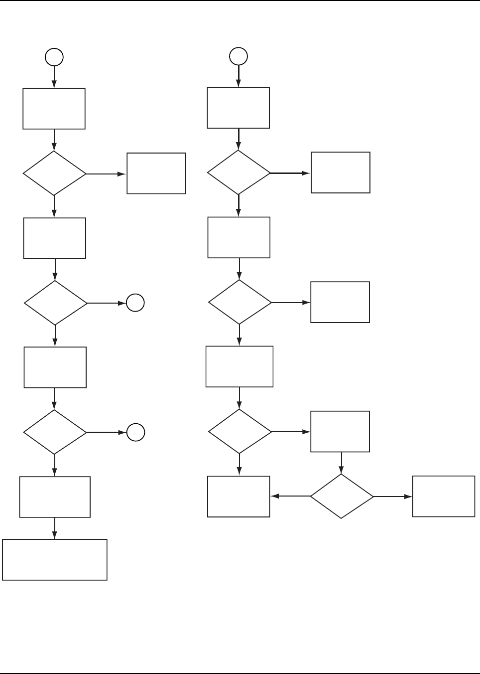
October 14, 2003 6881094C31-C
5-32 Troubleshooting Charts: TX RF (UHF R1/700-800 MHz)
TX RF (UHF R1/700-800 MHz)—Page 2
MAEPF-27420-B
RAWB+
about
7.2 Vdc?
Measure
RAWB+
at Q107-drain
No
No
No
Yes
Yes
Yes
Check
continuity
V.gate
about 2 to
3 Vdc?
Check
continuity
DC bias is OK,
control is OK,
RFIN is OK,
PA has low gain
Replace
Q107
No
Yes Measure RF
level at
pin 6 of Q107
Is
unit
VHF?
No Yes Remove SH101
and check for
parts off pad
Level
about
+35 dBm?
Replace U102.
For VHF, check under
SH101. if all parts soldered,
replace U102.
Measure
gate bias
at L108
RAWB+
about
7.2 Vdc?
Measure
RAWB+
at U102-6
No
No
Yes
Yes
TX7V
about
7.2 Vdc?
Check
continuity
Measure
Vgate at TP111,
normally 4 to
5.5 Vdc
Measure
TX7V at
U102-14
DC bias is OK,
control is OK,
RFIN is OK, driver
has low gain
Vgate
> 4 Vdc?
2
1
3
4

6881094C31-C October 14, 2003
Troubleshooting Charts: TX RF (UHF R1/700-800 MHz) 5-33
TX RF (UHF R1/700-800 MHz)—Page 3
INT > 5 Vdc?
Vgate at TP111
is low (< 4 Vdc)
Measure INT
at TP104
Yes
No
No
Yes
Yes
No
Replace
Q108
INT is low.
Measure VLIM
at TP119
PCIC is
programmed.
Measure TEMP
at R130
Bad PCIC
Replace U104
VLIM
about 2 to
3 Vdc?
No
Yes
Measure
RFIN at
TP101
TEMP
< 1.0 Vdc at
25C?
RFIN is low, INT
is low, bad PCIC,
replace U104
TP101
< 0.5 Vdc?
Low output power,
RFIN is high, check
RF detectors and
op amp U106.
Repair defects
Repair temperature
sensor circuit
(U103, Q109,
R130)
4
4
TXINH
< 1 Vdc?
TX7V is low.
Measure TXINH
at P1-19, Q101-b
No
No
Yes
Yes
RXH
< 1 Vdc?
No
Yes
Bad PCIC
Replace U104
RXH
> 5 Vdc?
Bad control
signal from
VOCON
Trace dc levels
through switching
transistors Q101,
Q102, Q103,
and Q106
Replace bad
transistors
Measure RXH
at U104-23
and Q103-b
3
MAEPF-27476-O
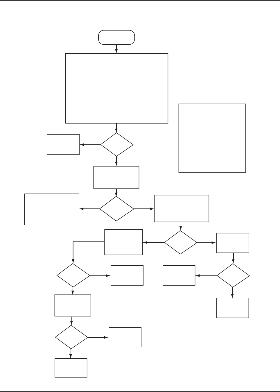
October 14, 2003 6881094C31-C
5-34 Troubleshooting Charts: Keyload Failure
5.17 Keyload Failure
MAEPF-27388-B
No
No
Yes
Yes
No
Keyload Failure
"KEYLOAD"
message
displayed?
With KVL attached to radio
and radio on, initiate a
keyload by pressing PTT on
the keyloader and look for
activity on J701-1
Yes Verify
connection
across J701
Repair
connection
Correct
equipment?
Obtain correct
KVL and
cable
No
Verify and repair
connection of UC_CTS,
UC_RS232DIN_USB-,
and UC_OPT_SEL2 signals
from KVL to universal
connector to J101
Verify the use of the correct secure kit and key loader:
With KVL attached to
radio and radio on,
verify display
message "KEYLOAD"
Activity?
Verify connection
of KEYFAIL
from the universal
connector pin 13 to
J101-2 and D301
Yes
No Good
connection?
Repair
connection
Replace
secure
module
Yes
Good
connection?
Verify operation of
voltage translator
circuit by seeing
activity on R315
No Replace
translator
circuit
Yes
Translator
circuit OK?
Replace
VOCON
board
This failure relates only to secure-
equipped radios and indicates a
failure to load key with the KVL
indicated by the message
"KEYFAIL" and key-fail tone.
Typical failure modes would be:
1) Open between universal
connector uC which places radio
in Keyload mode.
2) Use of wrong KVL or KVL cable
for XTS 5000 radio.
3) Failure of secure module.
Synopsis
XTS 5000 UCM Kits:
Software Kits:
NNTN4006A - DES, DES-XL, DES-OFB
NTN9837A - DES, DES-XL, DES-OFB with DVP-XL
NTN9838A - DVI-XL
NTN9839A - DVP-XL
NNTN4197 - AES
NNTN4198 - AES with DES, DES-XL, DES-OFB
Hardware Kits:
NTN9738C
NNTN5032A
Use KVL - 3000 or later model Keyloader. Use with
cable TDN9390.
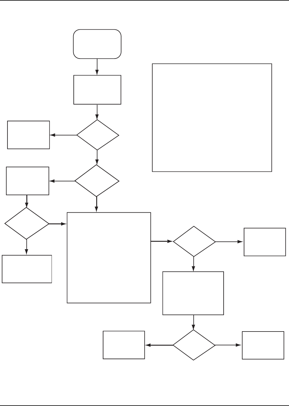
6881094C31-C October 14, 2003
Troubleshooting Charts: Secure Hardware Failure 5-35
5.18 Secure Hardware Failure
MAEPF-27387-O
Yes
No
Yes
No
No
No
Fail
09/10 or 09/90
Secure Hardware
Failure
Connections
good?
Repair
connections
Yes Replace
secure
module
Verify electrical activity
at the following signals
at power up:
Connections
good?
Repair
opens
No
Yes
Is
known good
module
available?
Replace module
with known good
one and retest
Verify connections
to secure module
through J701
Signals
good?
Yes
Replace
secure
module
Radio
functions with
known good
module?
Replace
respective
source IC or
VOCON board
This failure relates only to secure-equipped
radios and indicates a power-up self-test failure
for the secure module. More specifically this
failure indicates a failure in communications
between the DSP and secure module. The
secure module is not considered field repairable
so troubleshooting is limited to verifying a
problem with the module and replacing.
Typical failure modes would be:
1) Open between secure module and VOCON
board at J701.
2) Failure of the SSI bus that the DSP uses to
communicate with the secure module.
3) Failure to get proper supplies and grounds
to J701.
Synopsis
Use ohmmeter to electrically
verify the following signal
connections to source IC:
Signal @ J701 Source
ENC_SSI_DI R403
ENC_SSI_DO R402
ENC_SSI_CLK R405
RESET_ENC R418
Verify bias of following signals:
Signal @ J701 Nominal Bias
UNSW_B+ 7.5VDC+/-1.0VDC
SW_B+ 7.5VDC+/-1.0VDC
GND GND Signal @ J701 Source
ENC_SSI_DI R403
ENC_SSI_CLK R405

October 14, 2003 6881094C31-C
5-36 Troubleshooting Charts: Secure Hardware Failure
Notes
Chapter 6 Troubleshooting Waveforms
This chapter contains images of waveforms that might be useful in verifying operation of certain parts
of the circuitry. These waveforms are for reference only; the actual data depicted will vary depending
on operating conditions.
6.1 List of Waveforms
Table 6-1 lists each waveform and the page on which the waveform can be found.
Table 6-1. List of Waveforms
Waveform Page No.
13 MHz Clock 6-2
16.8 MHz Buffer Input and Output 6-3
32.768 kHz Clock Outputs 6-4
SPI B Data 6-5
Receive Serial Audio Port (SAP) 6-6
Receive Baseband Interface Port (RX BBP) 6-7
Transmit Baseband Interface Port (TX BBP) 6-8
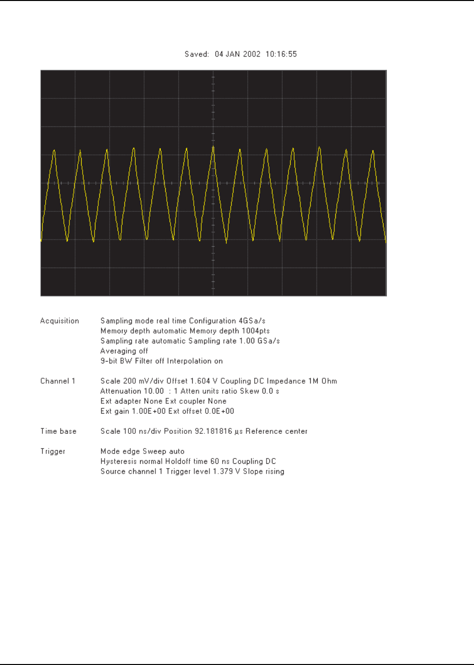
October 14, 2003 6881094C31-C
6-2 Troubleshooting Waveforms: 13 MHz Clock
6.2 13 MHz Clock
13 MHz clock from U301 to U501.
Trace 1: Trace recorded at C303 on the NTN9564 board.
Similar waveform is visible on C339 on the NNTN4563, NNTN4819, & NNTN4717 VOCON
boards.
Figure 6-1. 13 MHz Clock Waveform
MAEPF-27490-O
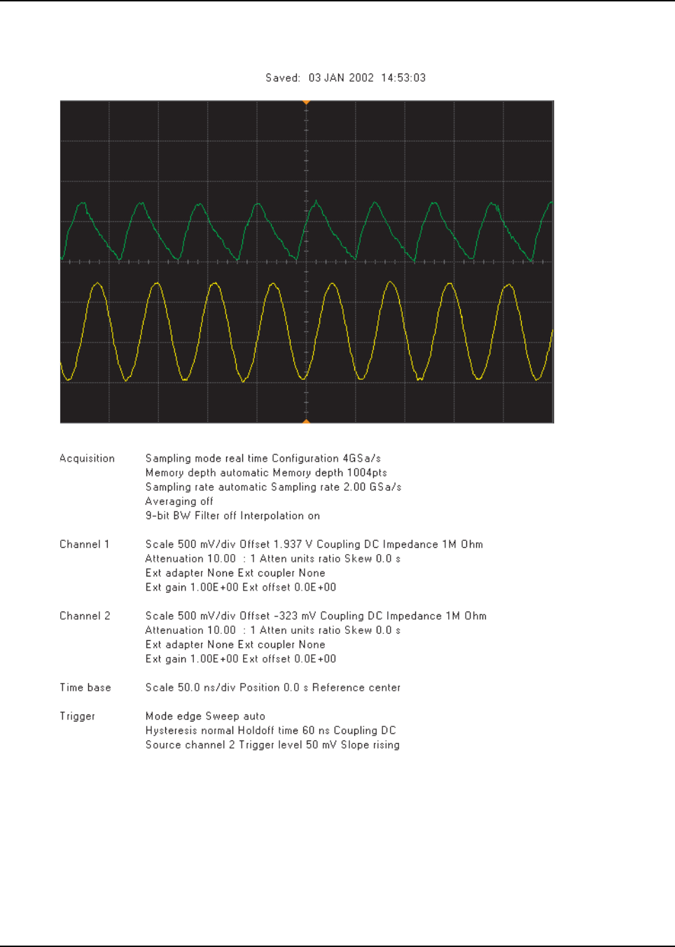
6881094C31-C October 14, 2003
Troubleshooting Waveforms: 16.8 MHz Buffer Input and Output 6-3
6.3 16.8 MHz Buffer Input and Output
Trace 1: Buffer input at R452.
Trace 2: Buffer output at C452.
Note: These components are under shield SH101 on the NNTN4563, NNTN4819, & NNTN4717
VOCON boards.
Figure 6-2. 16.8 MHz Buffer Input and Output Waveforms
MAEPF-27491-O
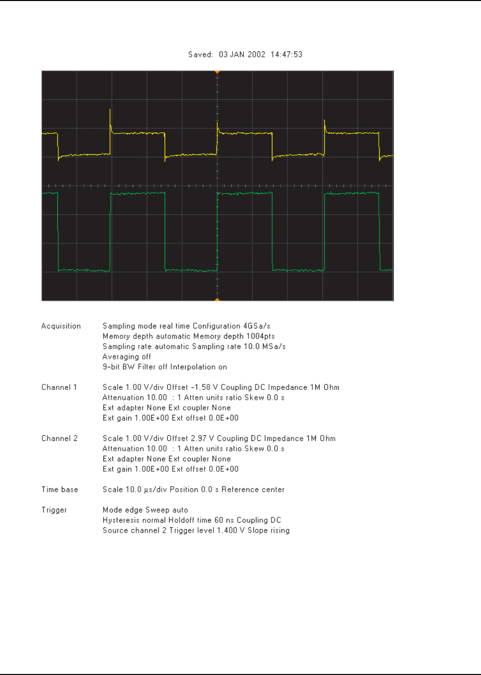
October 14, 2003 6881094C31-C
6-4 Troubleshooting Waveforms: 32.768 kHz Clock Outputs
6.4 32.768 kHz Clock Outputs
Trace 1: Output at C313 (to real-time clock of GCAP II IC).
Trace 2: Output at U302, pin 2 (to Patriot IC CKIL input).
Note: These components are under shield SH102 on the NNTN4563, NNTN4819, & NNTN4717
VOCON boards.
Figure 6-3. 32.768 kHz Clock Outputs Waveforms
MAEPF-27492-O
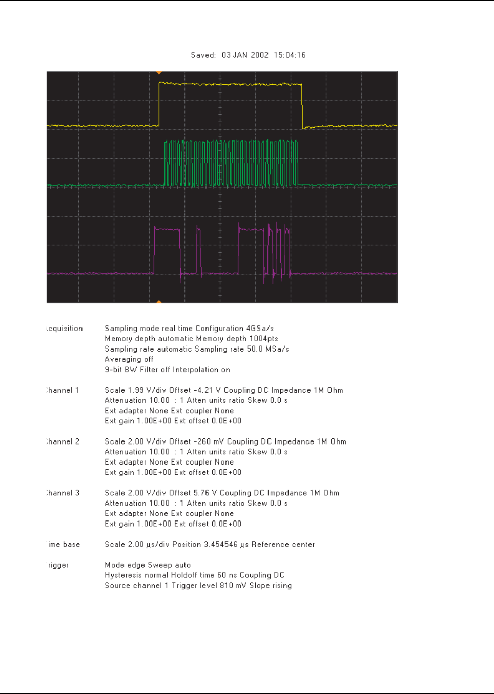
6881094C31-C October 14, 2003
Troubleshooting Waveforms: SPI B Data 6-5
6.5 SPI B Data
Trace 1: GCAP II IC chip enable at R539 (Note active high).
Trace 2: SPI data clock at Test Point SCKB.
Trace 3: SPI data to GCAP II IC at Test Point MOSIB.
Figure 6-4. SPI B Data Waveforms
MAEPF-27493-O
October 14, 2003 6881094C31-C
6-6 Troubleshooting Waveforms: Receive Serial Audio Port (SAP)
6.6 Receive Serial Audio Port (SAP)
Trace 1: 8 kHz frame sync at R406 (each word is 13 bits after failing edge of FSYNC).
Trace 2: SAP data at R403 (audio data from GCAP II IC CODEC to Patriot IC DSP).
Note: Transmit is identical, except data acquired at R402.
Trace 3: 520 kHz bit clock at R405 on the NTN9564, NNTN4563 & NNTN4819 VOCON boards.
256 kHz bit clock at R405 on the NNTN4717 VOCON board.
Figure 6-5. Receive Serial Audio Port (SAP) Waveforms
MAEPF-27494-O
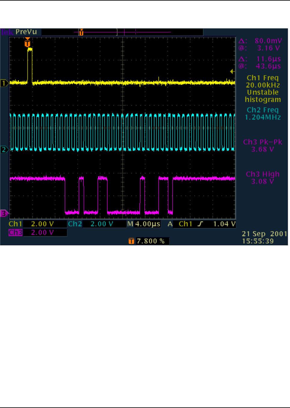
6881094C31-C October 14, 2003
Troubleshooting Waveforms: Receive Baseband Interface Port (RX BBP) 6-7
6.7 Receive Baseband Interface Port (RX BBP)
Trace 1: BBP RX frame sync signal at R123.
Trace 2: BBP RX clock signal at R124.
Trace 3: BBP RX data signal at R121.
Figure 6-6. Receive Baseband Interface Port (RX BBP) Waveforms
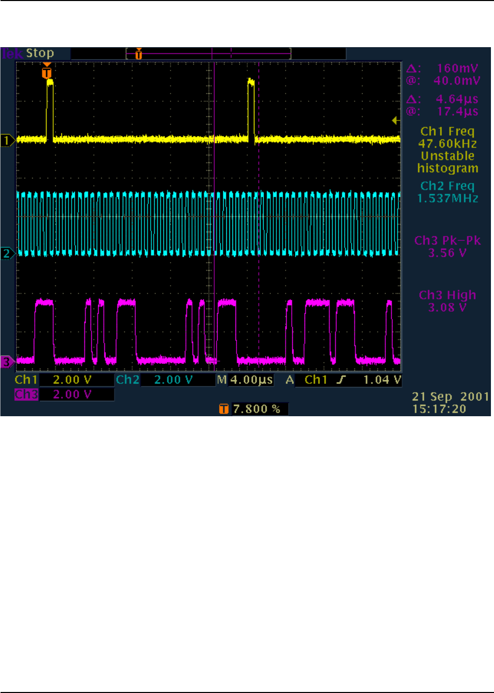
October 14, 2003 6881094C31-C
6-8 Troubleshooting Waveforms: Transmit Baseband Interface Port (TX BBP)
6.8 Transmit Baseband Interface Port (TX BBP)
Trace 1: BBP TX frame sync signal at R119.
Trace 2: BBP TX clock signal at R125.
Trace 3: BBP TX data signal at R127.
Figure 6-7. Transmit Baseband Interface Port (TX BBP) Waveforms
Chapter 7 Troubleshooting Tables
7.1 List of Board and IC Signals
Due to the nature of the schematic-generating program, signal names might be different when they
are not directly connected to the same point. The tables in this chapter provide a cross reference to
the various pinouts for these signals. Table 7-1 lists and provides links to each of the tables in this
chapter.
Table 7-1. List of Tables of Board and IC Signals
Table No. Table Name Page No.
7-2 J101 VOCON Board to Controls Flex Assembly 7-1
7-3 J107 VOCON Board to Keypad Module 7-3
7-4 J701 VOCON Board to Encryption Module 7-3
7-5 U402 FLASH Pinouts 7-5
7-6 U403 SRAM Pinouts 7-7
7-7 U401 Patriot MCU/DSP IC Pinouts 7-9
7-8 U301 Flipper IC Pinouts 7-18
7-9 U501 GCAP II IC Pinouts 7-20
Table 7-2. J101 VOCON Board to Controls Flex Assembly
J101
Pin No. Description To/From Side
Connector
Number
1 UC_CTS TP208 10
2 UC_LHDATA_KEYFAIL TP206 13
3 DGND03 TP202 8
4 UC_RS232DIN_USB- R253 12
5 UC_EXT_SPKR_NEG- TP213 6
6 UC_RS232DOUT_USB+ R252 11
7 UC_OPT_SEL2 R218 5
8 UC_SB9600_BUSY TP207 9
9 UC_EXT_SKPR TP212 2
10 UC_RTS TP209 7
October 14, 2003 6881094C31-C
7-2 Troubleshooting Tables: List of Board and IC Signals
11 UC_OPT_SEL1 R217 1
12 UC_OPTB+_VPP R255 4
13 UC_EXT_MIC TP214 3
14 UC_EMERG R233
15 DGND15 TP202
16 DGND16 TP202
17 UC_MONITOR R244
18 DGND18 TP202
19 DGND19 TP202
20 UC_BL_FREQ R206
21 UC_RED_LED R203
22 UC_GREEN_LED R204
23 UC_TG2 R234
24 UC_RTA1 R236
25 UC_RTA3 R241
26 UC_RTA2 R239
27 UC_RTA0 R235
28 DGND28 TP202
29 DGND29 TP202
30 DGND30 TP202
31 UC_VOLUME R232
32 BSENS_1 L202
33 UNSWB+1 L201
34 UC_TG1 R231
35 V2A L203
36 UC_INT_MICU L208
37 C_INT_SPKR_NEG TP213
38 UC_INT_PTT R216
39 AGND39 L204
40 UC_INT_SPKR L205
Table 7-2. J101 VOCON Board to Controls Flex Assembly (Continued)
J101
Pin No. Description To/From Side
Connector
Number
6881094C31-C October 14, 2003
Troubleshooting Tables: List of Board and IC Signals 7-3
Table 7-3. J107 VOCON Board to Keypad Module
J107
Pin No. Description To/From Accessible
on
VOCON?
1 KP_COLUMN0 C134 Yes
2 KP_COLUMN1 C133 Yes
3 KP_COLUMN2 C132 Yes
4 KP_GND GROUND Yes
5 KP_GND GROUND Yes
6 KP_BL_EN C124 Yes
7 KP_5V1 C104 Yes
8 KP_5V2 C104 Yes
9 KP_GND GROUND Yes
10 KP_GND GROUND Yes
11 KP_GND GROUND Yes
12 KP_GND GROUND Yes
13 KP_ROW0 C131 Yes
14 KP_ROW1 C130 Yes
15 KP_ROW2 C129 Yes
16 KP_ROW3 C128 Yes
17 KP_ROW4 C127 Yes
18 KP_ROW5 C126 Yes
19 KP_ROW6 C125 Yes
20 KP_GND GROUND Yes
21 KP_GND GROUND Yes
22 KP_GND GROUND Yes
Table 7-4. J701 VOCON Board to Encryption Module
J701
Pin No. Description To/From Accessible
on VOCON?
1 KEYFAIL_LH_BDMDATA Q303 Pin 2 Yes
2 RS232_DIN_ENC R308 Yes
3 RS232_DIN_UP R308 Yes
4 RTSIN_ENC U301 Pin H7 No
October 14, 2003 6881094C31-C
7-4 Troubleshooting Tables: List of Board and IC Signals
5 RS232_DOUT_UP R317 Yes
6 RS232_DOUT_ENC R317 Yes
7 SW_B+_ENC C101 Yes
8 Regulated V_ENC No Connect N/A
9 RS232_DTR_IN_ENC No Connect N/A
10 RS232_RI_OUT_EN No Connect N/A
11 USB_MINUS Monitor No Connect N/A
12 CONT_3VDC_OUT_ENC No Connect N/A
13 RS232_DCD_ENC No Connect N/A
14 USB_PLUS Monitor No Connect N/A
15 BOOT_ENC R417 Yes
16 TAMPER GROUND Yes
17 SSI_DO_CODEC_ENC R403 Yes
18 SSI_DI_CODEC_ENC R402 Yes
19 RTA0_ENC R246 Yes
20 RTA1_ENC R247 Yes
21 RTA3_ENC R251 Yes
22 RTA2_ENC R250 Yes
23 TG2_ENC R234 Yes
24 LHDATA_BDMDATA_KEYFAIL D308 Pin 3 Yes
25 GREEN_LED_ENC R204 Yes
26 WAKEUP U401 Pin E1 No
27 TX_INHIBIT R109 Yes
28 UCM_SS U301 Pin G4 No
29 RED_LED_ENC R203 Yes
30 RESET_ENC R418 Yes
31 MONITOR R244 Yes
32 SPARE1_ENC R415 Yes
33 GROUND_ENC GROUND Yes
34 SPARE2_ENC R416 Yes
35 EMERG_ENC R241 Yes
Table 7-4. J701 VOCON Board to Encryption Module (Continued)
J701
Pin No. Description To/From Accessible
on VOCON?
6881094C31-C October 14, 2003
Troubleshooting Tables: List of Board and IC Signals 7-5
36 UNSW_B+_ENC C102 Yes
37 ENC_SSI_CLK R404 Yes
38 ENC_SSI_FS R406 Yes
39 ENC_SSI_DI R403 Yes
40 ENC_SSI_DOUT R402 Yes
* = Component located under a shield on NNTN4563, NNTN4819, & NNTN4717
Table 7-5. U402 FLASH Pinouts
U402
Pin No. Description To/From Comment Accessible
on Vocon?
B4 B_CLK B_CLK** Yes
E7 CS0 CS0 Active Low Yes
F8 EN_OE No
C5 EN_WE No
D6 WRITE PROTECT No
C4 ADV ADV** Yes
B5 RESET D401, pin 2 1.875 V Yes
E8 ADDRESS 1 No
D8 ADDRESS 2 No
C8 ADDRESS 3 No
B8 ADDRESS 4 No
A8 ADDRESS 5 No
B7 ADDRESS 6 No
A7 ADDRESS 7 No
C7 ADDRESS 8 No
A2 ADDRESS 9 No
B2 ADDRESS 10 No
C2 ADDRESS 11 No
A1 ADDRESS 12 No
B1 ADDRESS 13 No
C1 ADDRESS 14 No
Table 7-4. J701 VOCON Board to Encryption Module (Continued)
J701
Pin No. Description To/From Accessible
on VOCON?

October 14, 2003 6881094C31-C
7-6 Troubleshooting Tables: List of Board and IC Signals
D2 ADDRESS 15 No
D1 ADDRESS 16 No
D4 ADDRESS 17 No
B6 ADDRESS 18 No
A6 ADDRESS 19 No
C6 ADDRESS 20 No
B3 ADDRESS 21 No
C3 ADDRESS 22 No
D7 ADDRESS 23 R427* Yes
A3 GROUND No
F1 GROUND No
G2 GROUND No
G8 GROUND No
E2 DATA 15 No
F2 DATA 14 No
F3 DATA 13 No
D5 DATA 12 No
F4 DATA 11 No
F5 DATA 10 No
F6 DATA 9 No
G7 DATA 8 No
G1 DATA 7 R435** Yes
E3 DATA 6 R434** Yes
G3 DATA 5 R433** Yes
E4 DATA 4 R432** Yes
G5 DATA 3 R431** Yes
E5 DATA 2 R430** Yes
E6 DATA 1 R429** Yes
F7 DATA 0 R428** Yes
A5 VPP D402, pin 3 1.875 V Yes
G6 VSW2 C409* 1.875 V Yes
Table 7-5. U402 FLASH Pinouts (Continued)
U402
Pin No. Description To/From Comment Accessible
on Vocon?
6881094C31-C October 14, 2003
Troubleshooting Tables: List of Board and IC Signals 7-7
E1 VSW2 C409* 1.875 V Yes
G4 VSW2 C409* 1.875 V Yes
A4 VSW2 C409* 1.875 V Yes
* = Component located under a shield on NNTN4563, NNTN4819, & NNTN4717
** = No test point/component on NNTN4563, NNTN4819, & NNTN4717 - signal not
accessible
Table 7-6. U403 SRAM Pinouts
U403
Pin No. Description To/From Comment Accessible
on Vocon?
A2 EN_OE No
G5 R_W R_W W = 0 V Yes
A1 LB No
B2 UB No
B5 CS1 CS2 (TP) Active Low Yes
A6 CS2 C411* Active Low Yes
A3 ADDRESS 1 Yes
A4 ADDRESS 2 Yes
A5 ADDRESS 3 Yes
B3 ADDRESS 4 Yes
B4 ADDRESS 5 Yes
C3 ADDRESS 6 Yes
C4 ADDRESS 7 Yes
D4 ADDRESS 8 No
H2 ADDRESS 9 No
H3 ADDRESS 10 No
H4 ADDRESS 11 No
H5 ADDRESS 12 No
G3 ADDRESS 13 No
G4 ADDRESS 14 No
F3 ADDRESS 15 No
F4 ADDRESS 16 No
Table 7-5. U402 FLASH Pinouts (Continued)
U402
Pin No. Description To/From Comment Accessible
on Vocon?
October 14, 2003 6881094C31-C
7-8 Troubleshooting Tables: List of Board and IC Signals
E4 ADDRESS 17 No
D3 ADDRESS 18 No
H1 ADDRESS 19 No
D1 GROUND No
E6 GROUND No
E3 GROUND No
H6 NOT USED No
G2 NOT USED No
G1 DATA 15 No
F1 DATA 14 No
F2 DATA 13 No
E2 DATA 12 No
D2 DATA 11 No
C2 DATA 10 No
C1 DATA 9 No
B1 DATA 8 No
G6 DATA 7 R435** No
F6 DATA 6 R434** No
F5 DATA 5 R433** No
E5 DATA 4 R432** No
D5 DATA 3 R431** No
C6 DATA 2 R430** No
C5 DATA 1 R429** No
B6 DATA 0 R428** No
D6 VSW2 C411* 1.875 V Yes
E1 VSW2 C411* 1.875 V Yes
* = Component located under a shield on NNTN4563, NNTN4819, & NNTN4717
** = No test point/component on NNTN4563, NNTN4819, & NNTN4717 - signal not
accessible
Table 7-6. U403 SRAM Pinouts (Continued)
U403
Pin No. Description To/From Comment Accessible
on Vocon?
6881094C31-C October 14, 2003
Troubleshooting Tables: List of Board and IC Signals 7-9
Table 7-7. U401 Patriot MCU/DSP IC Pinouts
U401
Pin No. Description To/From Comment Accessible
on Vocon?
H10 EEPOT_INC* C537 Active Low Yes
J14 EXT_SPKR_SEL Q505, pin 5 Yes
C14 AUDIO_PA_EN R575 Yes
B14 HOST_WAKE No
F6 BATTERY_ID C556 Yes
E5 MECH_SW_BAR Q508, pin 3 Active Low Yes
J6 INT_PTT R216 Active Low Yes
J5 GCAP_INT R538 Yes
J4 OPT_SEL1_IN U201 pin 1 Yes
J3 UART_INT* No
C16 8KHZ_INT R406 8 kHz Pulse Yes
G11 OPT_SEL2_IN U202 pin 1 Yes
F1 KP_ROW0 C131 Yes
H4 KP_ROW1 C130 Yes
H6 KP_ROW2 C129 Yes
G2 KP_ROW3 C128 Yes
G11 KP_ROW4 C127 Yes
G7 KP_ROW5 C126 Yes
H7 KP_ROW6 C125 Yes
H1 SPARE1_ENC J701, pin 32 Yes
D1 KP_COL0 C134 Yes
G5 KP_COL1 C133 Yes
F3 KP_COL2 C132 Yes
G4 ENC_RESET J701, pin 30 Yes
F2 BOOT* J701, pin 15 Yes
E1 WAKEUP J701, pin 26 Yes
H6 SPARE2_ENC J701, pin 34 Yes
G3 NOT USED No
E7 NOT USED No
A8 NOT USED No
F8 MISOA_SEL U406, pin 2 Yes

October 14, 2003 6881094C31-C
7-10 Troubleshooting Tables: List of Board and IC Signals
E8 NOT USED No
G8 NOT USED No
C3 NOT USED No
D4 LOCK_DET C123 Active Low Yes
A2 TG2 R234 Yes
B2 RTA3 R241 Yes
A3 RTA2 R239 Yes
B3 RTA1 R236 Yes
B4 RTA0 R235 Yes
A7 VSW2 E401* 1.875 V Yes
P3 VSW2 E401* 1.875 V Yes
P6 VSW2 E401* 1.875 V Yes
T9 VSW2 E401* 1.875 V Yes
N10 VSW2 E401* 1.875 V Yes
R16 VSW2 E401* 1.875 V Yes
H9 V2 E402* 3.0 V Yes
G9 V2 E402* 3.0 V Yes
E15 V2 E402* 3.0 V Yes
A16 V2 E402* 3.0 V Yes
K10 V2 E402* 3.0 V Yes
C12 V2 E402* 3.0 V Yes
D8 V2 E402* 3.0 V Yes
B7 V2 E402* 3.0 V Yes
A4 V2 E402* 3.0 V Yes
A16 V2 E402* 3.0 V Yes
H2 V2 E402* 3.0 V Yes
K3 VSW2 E401* 1.875 V Yes
R8 VSW2 E401* 1.875 V Yes
G15 VSW2 E401* 1.875 V Yes
C10 VSW2 E401* 1.875 V Yes
K12 URXD1_USB_VMI No
Table 7-7. U401 Patriot MCU/DSP IC Pinouts (Continued)
U401
Pin No. Description To/From Comment Accessible
on Vocon?
6881094C31-C October 14, 2003
Troubleshooting Tables: List of Board and IC Signals 7-11
L16 URTS1_XRXD No
F13 ADTRIG No
B16 URXD2 U303, pin 4 Yes
D14 BSY_IN_RTS No
B12 RX_SSI_DATA R123 Data From
Abacus to
DSP
Yes
C11 TX_SSI_CLK R125 1.536 MHz Yes
B10 RED_LED Q201, pin 3 Active High Yes
D10 GREEN_LED Q201, pin 5 Active High Yes
B11 TX_SSI_FSYNC R119 48 kHz Yes
J10 CODEC_TX R402 GCAP to DSP
Tx Audio Data Yes
J15 CODEC_DCLK R405 520 kHz
(NTN9564
NNTN4563
NNTN4819)
256 kHz
(NNTN4717)
Yes
K16 CODEC_FSYNC R406 8 kHz Pulse Yes
D7 SPI_MISOA MISOA SPI A Data In Yes
D3 SPI_MISOB MISOB SPI B Data In Yes
E6 NOT USED No
F7 NOT USED No
D6 EEPROM_SEL* R132 Active Low Yes
C5 AD_CS* R133 Active Low Yes
A9 NOT USED No
B8 NOT USED No
B9 NOT USED No
A10 NOT USED No
G6 BT_DISABLE No
D13 NOT USED No
S15 BT_WAKE No
F11 RX_SSI_CLK R124 Yes
Table 7-7. U401 Patriot MCU/DSP IC Pinouts (Continued)
U401
Pin No. Description To/From Comment Accessible
on Vocon?
October 14, 2003 6881094C31-C
7-12 Troubleshooting Tables: List of Board and IC Signals
B15 OPT_SEL2_OUT R256 Yes
J13 AUDIO_MODE_SEL R257 Yes
J16 EEPOT_CS_EXT* U509, pin 1 Yes
J12 EEPOT_U_D* U509, pin 2 Yes
H11 EEPOT_CS* U509, pin 10 Yes
A5 GROUND GROUND Yes
N6 GROUND GROUND Yes
P8 GROUND GROUND Yes
P11 GROUND GROUND Yes
M11 GROUND GROUND Yes
L15 GROUND GROUND Yes
H16 GROUND GROUND Yes
F14 GROUND GROUND Yes
G14 GROUND GROUND Yes
E13 GROUND GROUND Yes
B13 GROUND GROUND Yes
K15 GROUND GROUND Yes
D9 GROUND GROUND Yes
C8 GROUND GROUND Yes
B5 GROUND GROUND Yes
C2 GROUND GROUND Yes
C1 GROUND GROUND Yes
H3 GROUND GROUND Yes
K15 GROUND GROUND Yes
T8 GROUND GROUND Yes
H15 GROUND GROUND Yes
C9 GROUND GROUND Yes
B6 ABACUS_CS* R126 Active Low Yes
E2 UNI_SEL* R131 Active Low Yes
D2 FLPR_CS* Active Low No
E3 GCAP_CE R539 Active High Yes
Table 7-7. U401 Patriot MCU/DSP IC Pinouts (Continued)
U401
Pin No. Description To/From Comment Accessible
on Vocon?
6881094C31-C October 14, 2003
Troubleshooting Tables: List of Board and IC Signals 7-13
E4 SCKB SCKB SPI B Clock Yes
B1 NOT USED No
F4 NOT USED No
F5 SPI_MOSIB MOSIB SPI Data Out Yes
C7 SCKA SCKA SPI A Clock Yes
C6 MOSIA MOSIA SPI Data Out Yes
G10 NOT USED No
G16 OPT_SEL1_OUT U201, pin 3 Yes
J11 CODEC_RX R403 DSP to GCAP
Rx Audio Data Yes
A12 RX_SSI_FSYNC R123 20 kHz pulse Yes
A11 RX_SSI_CLK R124 1.2 MHz Yes
E9 TX_SSI_DATA R127 Data From
DSP to A/D Yes
C15 BSY_OUT_CTS* No
F12 UTXD2 U303, pin 1* Yes
D15 USB_SUSP No
E14 DISPLAY_R_W* D403, pin 3 W = 0 V Yes
D16 NOT USED No
G12 UCTS1_USB_SPEED* No
K11 UTXD1_USB_VPO No
K14 USB_VMO No
K13 USB_TX_EN No
D5 8 KHZ_INT R406 8 kHz Pulse Yes
H14 BL_EN C124 Yes
K4 LV_DETECT POR 3.0 V Yes
F9 NOT USED No
J2 NOT USED No
A6 16_8_MHZ C452* 16.8 MHz Yes
Table 7-7. U401 Patriot MCU/DSP IC Pinouts (Continued)
U401
Pin No. Description To/From Comment Accessible
on Vocon?
October 14, 2003 6881094C31-C
7-14 Troubleshooting Tables: List of Board and IC Signals
J7 FLIP_32K 32 kHZ
(NTN9564)
U302, pin 2*
(NNTN4563
NNTN4819
NNTN4717)
32.768 kHz Yes
G13 NOT USED No
J11 MOD MOD Bootstrap
mode > 2.7 V Yes
A13 NOT USED No
M6 NOT USED No
R1 NOT USED No
N3 NOT USED No
M5 NOT USED No
P2 NOT USED No
P1 NOT USED No
N1 NOT USED No
M4 NOT USED No
M3 NOT USED No
M2 NOT USED No
M1 NOT USED No
L4 NOT USED No
L3 NOT USED No
L1 NOT USED No
L2 NOT USED No
K2 NOT USED No
T1 NOT USED No
R2 NOT USED No
T2 NOT USED No
K7 NOT USED No
N2 NOT USED No
L5 NOT USED No
L6 NOT USED No
C4 NOT USED No
Table 7-7. U401 Patriot MCU/DSP IC Pinouts (Continued)
U401
Pin No. Description To/From Comment Accessible
on Vocon?
6881094C31-C October 14, 2003
Troubleshooting Tables: List of Board and IC Signals 7-15
L13 NOT USED No
D11 ONE_WIRE_EN* Active Low No
E16 KVL_USB_DET* Active Low No
F15 NOT USED No
K5 BAT_BUS_EN* Q507, pin 2 Active Low Yes
H8 NOT USED No
F16 RESET RESET_OUT
(NTN9564)
D401, Pin 3
(NNTN4563
NNTN4819,
NNTN4717)
Reset = 0 V Yes
K6 USB_VPI No
H12 BL_FREQ Q202, pin 5 Active High Yes
H13 NOT USED No
E10 DSP_DE DSP_DE ONCE/JTAG Yes
F10 MCU_DE MCU_DE ONCE/JTAG Yes
D12 TCK TCK ONCE/JTAG Yes
C13 TMS TMS ONCE/JTAG Yes
E11 TRST TRST ONCE/JTAG Yes
A14 TDO TDO ONCE/JTAG Yes
E12 TDI TDI ONCE/JTAG Yes
M16 NOT USED No
L14 NOT USED No
P15 NOT USED No
L11 NOT USED No
M14 NOT USED No
N16 NOT USED No
L12 NOT USED No
M12 CKO CKO Disabled Yes
N15 NOT USED No
M15 NOT USED No
Table 7-7. U401 Patriot MCU/DSP IC Pinouts (Continued)
U401
Pin No. Description To/From Comment Accessible
on Vocon?
October 14, 2003 6881094C31-C
7-16 Troubleshooting Tables: List of Board and IC Signals
R12 ADDRESS 0 J101, pin 7 Not accessible
on NNTN4563,
NNTN4819, &
NNTN4717
Yes
T13 ADDRESS 1 No
M10 ADDRESS 2 No
T12 ADDRESS 3 No
P13 ADDRESS 4 No
M9 ADDRESS 5 No
P10 ADDRESS 6 No
P12 ADDRESS 7 No
N9 ADDRESS 8 No
R10 ADDRESS 9 No
P9 ADDRESS 10 No
L10 ADDRESS 11 No
T10 ADDRESS 12 No
R9 ADDRESS 13 No
L9 ADDRESS 14 No
K9 ADDRESS 15 No
J9 ADDRESS 16 No
L8 ADDRESS 17 No
M8 ADDRESS 18 No
N8 ADDRESS 19 No
K8 ADDRESS 20 No
L7 ADDRESS 21 No
T7 ADDRESS 22 No
R7 ADDRESS 23 R427* Yes
R3 DATA 15 No
T3 DATA 14 No
N4 DATA 13 No
P4 DATA 12 No
R4 DATA 11 No
Table 7-7. U401 Patriot MCU/DSP IC Pinouts (Continued)
U401
Pin No. Description To/From Comment Accessible
on Vocon?
6881094C31-C October 14, 2003
Troubleshooting Tables: List of Board and IC Signals 7-17
J8 DATA 10 No
T4 DATA 9 No
N5 DATA 8 No
P5 DATA 7 R435** Yes
R5 DATA 6 R434** Yes
T5 DATA 5 R433** Yes
R6 DATA 4 R432** Yes
T6 DATA 3 R431** Yes
M7 DATA 2 R430** Yes
N7 DATA 1 R429** Yes
P7 DATA 0 R428** Yes
N11 R_W R_W Yes
T11 NOT USED No
R14 NOT USED No
N12 CS3* R106** Active Low Yes
T14 CS2 CS2 Active Low Yes
R11 NOT USED No
R15 CS0 CS0 Active Low Yes
P16 OE_EN No
M13 EB1_N No
R13 EBO_N No
N14 NOT USED No
T16 WAIT WAIT** Yes
P14 NOT USED No
N13 ADV ADV** Yes
T15 B_CLK B_CLK** Yes
* = Component located under a shield on NNTN4563, NNTN4819, & NNTN4717
** = No test point/component on NNTN4563, NNTN4819, & NNTN4717 - signal not
accessible
Table 7-7. U401 Patriot MCU/DSP IC Pinouts (Continued)
U401
Pin No. Description To/From Comment Accessible
on Vocon?
October 14, 2003 6881094C31-C
7-18 Troubleshooting Tables: List of Board and IC Signals
Table 7-8. U301 Flipper IC Pinouts
U301
Pin No. Description To/From Comment Accessible
on Vocon?
E7 RXDIN_ENC_3V R308 Yes
D5 TXDO_BDI_5V R329* 5 V RS232
Data Out Yes
C7 RXDIN_5V R328* 5 V RS232
Data In Yes
A8 RTS D303 pin 3 Request to
Send (RS232) Yes
D7 CTS R303 Clear to Send
(RS232) Yes
H8 CTS_FILLREQ_3V R306** Yes
H3 16.8 MHz C307* 16.8 MHz
Clock Yes
H6 13 MHz R302
R331* 13 MHz Clock
(OUT) Yes
H5 PLL_LFT C302* PLL Loop
Filter Yes
F4 CODEC_DCLK R405 520 kHz Yes
E5 CODEC_FSYNC R406 8 kHz Pulse Yes
G4 UCM_SS J701 pin 28 Yes
G2 V2 C304* 3.0 V Yes
F1 V2 C317* 3.0 V Yes
F3 VSS3_DC GROUND Yes
F2 VSS3_AC GROUND Yes
D8 VCC5 C305* 5.0 V Yes
C8 VSS5 GROUND Yes
A7 LI_CELL C312* 3.0-3.3 V Yes
C6 VSS3_XTL GROUND Yes
A4 UART_TX NC No
C4 UART_RX NC No
G3 ONE_WIRE_UP No
G7 KVL_USB_DET No
G1 ONE_WIRE_EN* No
B5 BSY_IN_RTS No
C5 BSY_OUT_CTS No
E4 UCTS1_USB_SPEED* No
C1 USB_TXENAB No
6881094C31-C October 14, 2003
Troubleshooting Tables: List of Board and IC Signals 7-19
D1 UTXD1_USP_VPO No
B1 USB_VMO No
C3 URTS1_XRXD No
C2 USB_VPI No
D2 URXD1_USB_VMI No
E3 USB_SUSP No
B2 SCKB SCKB SPI B Clock Yes
B3 SPI_MOSIB MOSIB SPI Data Write
to Flipper IC Yes
A2 SPI_MISOB MISOA SPI Data Read
from Flipper IC Yes
A1 FLPR_CS* No
A3 UART_INT* No
F5 GCAP_RESET_X C310* Yes
H4 TEST_MODE1 GROUND Yes
H1 TES_MODE2 GROUND Yes
G6 OUT_DIS GROUND Yes
G5 SCAN_EN GROUND Yes
A6 XTAL32_IN Yes
B6 XTAL32_OUT Yes
A5 REF32_OUT R316 32.768 kHz
Square Wave Yes
B7 BYPASS_32 GROUND Yes
B4 BP_SEN_X R510 0 V Yes
D4 WD_OUT R528 Watchdog Int
to GCAP II Yes
H2 ONE_WIRE_OPT D306 pin 3 Yes
D6 SB96D_BDO_KF_5V NC No
B8 LH_BUSY D307 pin 3 Yes
D3 USB_DIS R310* Yes
E2 USB_DPLUS Q301 pin 1* USB Data Plus Yes
E1 USB_DMINUS Q301 pin 4* USB Data
Minus Yes
E8 SB96D_BDO_KF_3V NC No
F6 SB96D_BDO_3V D308 pin 3 Yes
Table 7-8. U301 Flipper IC Pinouts (Continued)
U301
Pin No. Description To/From Comment Accessible
on Vocon?
October 14, 2003 6881094C31-C
7-20 Troubleshooting Tables: List of Board and IC Signals
H7 RTS_FILLSEN_3V NC No
G8 CTS_FILLREQ_3V R309* Yes
F8 TXDO_BDI_ENC_3V R317 Yes
F7 TXDO_BDI_UP_3V R317 Yes
E6 RXDIN_ENC_3V R308 Yes
* = Component located under a shield on NNTN4563, NNTN4819, & NNTN4717
** = No test point/component on NNTN4563, NNTN4819, & NNTN4717 - signal not
accessible
Table 7-9. U501 GCAP II IC Pinouts
U501
Pin No. Description To/From Comment Accessible
on Vocon?
A2 AD4_BD_ID R525 Yes
B2 AD3_BDTYPE R524 Yes
B3 AD2_BAT_STAT R568 Yes
A3 AD_TG1 R523 Yes
D4 AD0_EMERG R522 Yes
C4 LV_DETECT R511 Active Low Yes
B4 AD_TRIG No
A4 CONV_BYP C516 Yes
B5 V3 C550 Unused
Voltage
Regulator
Yes
A5 VIN3 C515 3.77 V Yes
D5 VSEN1 GROUND 0 V Yes
C5 VSIN C515 3.77 V Yes
C6 VSIM1 C551 Unused
Voltage
Regulator
Yes
A6 V1 C552 Unused
Voltage
Regulator
Yes
B6 VIN1 B503 7.5V Yes
D6 LI_CELL C553 3.0-3.3V Yes
D7 CHARGE NC No
Table 7-8. U301 Flipper IC Pinouts (Continued)
U301
Pin No. Description To/From Comment Accessible
on Vocon?
6881094C31-C October 14, 2003
Troubleshooting Tables: List of Board and IC Signals 7-21
A7 XTAL1 G_32K 32.768 kHz
Square Wave Yes
B7 XTAL2 No
A8 PRSC2 C514 3.77V Yes
B8 LX2 D502 262.144 kHz
Square Wave Yes
A9 PGND1 GROUND Yes
B9 FB2 R501 1.85V Yes
C8 ON R579 Yes
A10 FB1 R502 3.77V Yes
B10 LX1 D503 262.144 kHz
Square Wave Yes
C9 PWRON C529 At Battery
Voltage Level Yes
D8 INT_EXT GROUND Yes
C10 PSRC1 C531 At Battery
Voltage Level Yes
E7 WDI R576 3.0V Yes
D10 MOSPORTB C529 At Battery
Voltage Level Yes
D9 ISENSE NC No
E8 CHRGC NC No
E9 SQ_OUT NC No
E10 BPOS C529 At Battery
Voltage Level Yes
F7 BATTERY NC No
F8 AUX_BAT NC No
F9 AUX_FET NC No
F10 MAIN_FET NC No
E6 PGM2 C529 At Battery
Voltage Level Yes
G8 PGM1 C529 At Battery
Voltage Level Yes
G10 AGND1 GROUND Yes
G9 REF C528 3.0V Yes
Table 7-9. U501 GCAP II IC Pinouts (Continued)
U501
Pin No. Description To/From Comment Accessible
on Vocon?
October 14, 2003 6881094C31-C
7-22 Troubleshooting Tables: List of Board and IC Signals
H9 PA_DRV NC No
H10 PA_SENSE NC No
G7 PGM0 GROUND Yes
H8 LS3_RX NC No
J10 DGND GROUND Yes
K10 LS3TX_PABPOS GROUND Yes
K1 MIC_OUT U509 pin 6 AC Mic Signal Yes
G4 STANDBY R557 3.0V Yes
K2 AUX_OUT U509 pin 6 AC Mic Signal Yes
H3 AUX_MIC_NEG C538 Virtual Ground Yes
J3 MB_CAP C535 Yes
H4 EXT_MIC NC No
K3 MIC_BIAS C535 Yes
J4 CD_CAP C543 Yes
K4 VAG C544 Yes
J5 V2 R560 3.0V Yes
K5 VIN2 R502 3.77V Yes
G5 ON2 NC No
H5 EXTOUT C533 AC RX Audio
Signal Yes
K6 SPKR_OUT NC No
J6 SPKR_IN NC No
H6 SPKR_NEG NC No
H7 SPKR_POS NC No
K7 LS1IN_TG1A GROUND Yes
J7 LS1OUT_TG1 NC No
G6 LS2IN_TG2A GROUND Yes
F6 LS2OUT_TG2 No
K8 ALRT_GND No
K9 ALRT_OUT NC No
J9 ALRT_VCC NC No
Table 7-9. U501 GCAP II IC Pinouts (Continued)
U501
Pin No. Description To/From Comment Accessible
on Vocon?
6881094C31-C October 14, 2003
Troubleshooting Tables: List of Board and IC Signals 7-23
J8 SIMI_O NC No
A1 AD5_VOLUME R526 0-2.5V Yes
B1 AGND3 GROUND Yes
C3 DWN_OUT NC No
C2 DWN_IN GROUND Yes
C1 CMP_OUT NC No
D3 DSC_INN GROUND Yes
D2 DSC_INP GROUND Yes
D1 SPI_CLK SCKB SPI Data
Clock Yes
E4 SPI_DR MISOB SPI Data Read
From GCAP Yes
E3 SPI_DW MOSIB SPI Data Write
To GCAP Yes
E2 SR_VCCIN NC No
E1 SR_VCCOUT NC No
F3 SR_IN NC No
F2 SR_OUT NC No
F1 INTERRUPT R538 GCAP
Interrupt Yes
F4 CE R539 Active High
GCAP Chip
EN
Yes
F5 CLK_IN R302
R331* 13 MHz Yes
E5 CODEC_DCLK R405 520 kHz
(NTN9564
NNTN4563
NNTN4819)
256 kHz
(NNTN4717)
Yes
G1 CODEC_TX R402 TX Audio Data
To DSP Yes
G2 CODEC_RX R403 RX Audio Data
From DSP Yes
G3 CODEC_FSYNC R406 8 kHz Frame
Sync Yes
Table 7-9. U501 GCAP II IC Pinouts (Continued)
U501
Pin No. Description To/From Comment Accessible
on Vocon?

October 14, 2003 6881094C31-C
7-24 Troubleshooting Tables: List of Board and IC Signals
H1 AGND4 GROUND Yes
J1 AGND2 GROUND Yes
H2 MICIN_POS C534 Yes
J2 MICIN_NEG Virtual Ground No
* = Component located under a shield on NNTN4563, NNTN4819, & NNTN4717
Table 7-9. U501 GCAP II IC Pinouts (Continued)
U501
Pin No. Description To/From Comment Accessible
on Vocon?

8-150 Schematics, Board Overlays, and Parts Lists: VOCON Boards
October 14, 2003 6881094C31-C
Notes

Appendix A Replacement Parts Ordering
A.1 Basic Ordering Information
When ordering replacement parts or equipment information, the complete identification number
should be included. This applies to all components, kits, and chassis. If the component part number
is not known, the order should include the number of the chassis or kit of which it is a part, and
sufficient description of the desired component to identify it.
Crystal orders should specify the crystal type number, crystal and carrier frequency, and the model
number in which the part is used.
A.2 Transceiver Board and VOCON Board Ordering Information
When ordering a replacement Transceiver Board or VOCON Board, refer to the applicable Model
Chart in the front of this manual, read the Transceiver Board or VOCON Board note, and include the
proper information with your order.
A.3 Motorola Online
Motorola Online users can access our online catalog at
https://www.motorola.com/businessonline
To register for online access, please call 800-814-0601 (for U.S. and Canada Service Centers only).
International customers can obtain assistance at https://businessonline.motorola.com.
A.4 Mail Orders
Send written orders to the following addresses:
* The Radio Products Services Division (RPSD) was formerly known as the Customer Care and
Services Division (CCSD) and/or the Accessories and Aftermarket Division (AAD).
Replacement Parts/
Test Equipment/Manuals/
Crystal Service Items
(United States and Canada):
Motorola Inc.
Radio Products Services Division*
Attention: Order Processing
1307 E. Algonquin Road
Schaumburg, IL 60196
U.S.A.
Federal Government Orders:
Motorola Inc.
U.S. Federal Government
Markets Division
Attention: Order Processing
7230 Parkway Drive
Landover, MD 21076
U.S.A.
International Orders:
Motorola Inc.
Radio Products Services Division*
(United States and Canada)
Attention: Order Processing
1307 E. Algonquin Road
Schaumburg, IL 60196
U.S.A.

October 14, 2003 6881094C31-C
A-2 Replacement Parts Ordering: Telephone Orders
A.5 Telephone Orders
Radio Products Services Division*
(United States and Canada)
7:00 AM to 7:00 PM (Central Standard Time)
Monday through Friday (Chicago, U.S.A.)
1-800-422-4210
(International Orders)
1-847-538-8023
U.S. Federal Government Markets Division (USFGMD)
1-800-826-1913 Federal Government Parts - Credit Cards Only
8:30 AM to 5:00 PM (Eastern Standard Time)
A.6 Fax Orders
Radio Products Services Division*
(United States and Canada)
1-800-622-6210
(International)
1-847-576-3023
USFGMD
(Federal Government Orders)
1-800-526-8641 (For Parts and Equipment Purchase Orders)
A.7 Parts Identification
Radio Products Services Division*
(United States and Canada)
1-800-422-4210, menu 3
A.8 Product Customer Service
Customer Response Center
(Non-technical Issues)
1-800-247-2346
FAX:1-800-247-2347
* The Radio Products Services Division (RPSD) was formerly known as the Customer Care and
Services Division (CCSD) and/or the Accessories and Aftermarket Division (AAD).

Glossary Glossary
This glossary contains an alphabetical listing of terms and their definitions that are applicable to
ASTRO portable and mobile subscriber radio products. All terms do not necessarily apply to all
radios, and some terms are merely generic in nature.
Term Definition
A/D See analog-to-digital conversion.
Abacus IC A custom integrated circuit providing a digital receiver intermediate
frequency (IF) backend.
ADC See analog-to-digital converter.
ADDAG See Analog-to-Digital, Digital-to-Analog and Glue.
ALC See automatic level control.
analog Refers to a continuously variable signal or a circuit or device designed
to handle such signals. See also digital.
Analog-to-Digital,
Digital-to-Analog
and Glue
An integrated circuit designed to be an interface between the radio’s
DSP, which is digital, and the analog transmitter and receiver ICs.
analog-to-digital
conversion Conversion of an instantaneous dc voltage level to a corresponding
digital value. See also D/A.
analog-to-digital
converter A device that converts analog signals into digital data. See also DAC.
automatic level
control A circuit in the transmit RF path that controls RF power amplifier output,
provides leveling over frequency and voltage, and protects against high
VSWR.
band Frequencies allowed for a specific purpose.
BBP See baseband interface port.
baseband interface
port Synchronous serial interface to the transceiver board used to transfer
transmit and receive audio data.
BGA See ball grid array.
ball grid array A type of IC package characterized by solder balls arranged in a grid
that are located on the underside of the package.
CODEC See coder/decoder.

October 14, 2003 6881094C31-C
Glossary-2
codeplug Firmware that contains the unique personality for a system or device. A
codeplug is programmable and allows changes to system and unit
parameters. See also firmware.
coder/decoder A device that encodes or decodes a signal.
CPS See Customer Programming Software.
Customer
Programming
Software
Software with a graphical user interface containing the feature set of an
ASTRO radio. See also RSS.
D/A See digital-to-analog conversion.
DAC See digital-to-analog converter.
Data communication
equipment Definition for device (such as radio) data communications using the
RS232 protocol. The correct data communication wiring requires the
device’s TX pins (output) to connect to the RX pins (input) and the RTS
pins (output) to connect to the CTS pins (input). It is incorrect to attach
device pins having the same name to to each other.
Data terminal
equipment Data terminal equipment; for example, a computer.
DCE See Data communication equipment.
default A pre-defined set of parameters.
digital Refers to data that is stored or transmitted as a sequence of discrete
symbols from a finite set; most commonly this means binary data
represented using electronic or electromagnetic signals. See also
analog.
digital-to-analog
conversion Conversion of a digital signal to a voltage that is proportional to the input
value. See also A/D.
digital-to-analog
converter A device that converts digital data into analog signals. See also ADC.
Digital Private-Line A type of digital communication that utilizes privacy call, as well as
memory channel and busy channel lock-out to enhance communication
efficiency.
digital signal
processor A microcontroller specifically designed for performing the mathematics
involved in manipulating analog information, such as sound, that has
been converted into a digital form. DSP also implies the use of a data
compression technique.
digital signal
processor code Object code executed by the Digital Signal Processor in an ASTRO
subscriber radio. The DSP is responsible for computation-intensive
tasks, such as decoding ASTRO signaling.
Term Definition

6881094C31-C October 14, 2003
Glossary-3
DPL See Digital Private-Line. See also PL.
DSP See digital signal processor.
DSP code See digital signal processor code.
DTE See Data terminal equipment.
DTMF See dual tone multi-frequency.
dual tone multi-
frequency The system used by touch-tone telephones. DTMF assigns a specific
frequency, or tone, to each key so that it can easily be identified by a
microprocessor.
EEPOT Electrically Programmable Digital Potentiometer.
EEPROM See Electrically Erasable Programmable Read-Only Memory.
Electrically Erasable
Programmable
Read-Only Memory
A special type of PROM that can be erased by exposing it to an
electrical charge. An EEPROM retains its contents even when the
power is turned off.
FCC Federal Communications Commission.
firmware Code executed by an embedded processor such as the Host or DSP in
a subscriber radio. This type of code is typically resident in non-volatile
memory and as such is more difficult to change than code executed
from RAM.
FGU See frequency generation unit.
flash A non-volatile memory device similar to an EEPROM. Flash memory
can be erased and reprogrammed in blocks instead of one byte at a
time.
FLASHcode A 13-digit code which uniquely identifies the System Software Package
and Software Revenue Options that are enabled in a particular
subscriber radio. FLASHcodes are only applicable for radios which are
upgradeable through the FLASHport process.
FLASHport A Motorola term that describes the ability of a radio to change memory.
Every FLASHport radio contains a FLASHport EEPROM memory chip
that can be software written and rewritten to, again and again.
FMR See Florida Manual Revision.
Florida Manual
Revision A document that provides interim updates to a publication until the
entire publication can be updated and reissued.
frequency Number of times a complete electromagnetic-wave cycle occurs in a
fixed unit of time (usually one second).
Term Definition

October 14, 2003 6881094C31-C
Glossary-4
frequency
generation unit This unit generates ultra-stable, low-phase noise master clock and other
derived synchronization clocks that are distributed throughout the
communication network.
General-Purpose
Input/Output Pins whose function is programmable.
GPIO See General-Purpose Input/Output.
host code Object code executed by the host processor in an ASTRO subscriber
radio. The host is responsible for control-oriented tasks such as
decoding and responding to user inputs.
IC See integrated circuit.
IF Intermediate Frequency.
IMBE A sub-band, voice-encoding algorithm used in ASTRO digital voice.
inbound signaling
word Data transmitted on the control channel from a subscriber unit to the
central control unit.
integrated circuit An assembly of interconnected components on a small semiconductor
chip, usually made of silicon. One chip can contain millions of
microscopic components and perform many functions.
ISW See inbound signaling word.
keep-alive mode A software-controlled operational mode in which power for the radio
remains on after the On/Off/volume control knob is turned off to allow
the microcontroller unit to complete its power-down sequence. Then,
the radio completely powers off.
key-variable loader A device used to load encryption keys into a radio.
kHz See kilohertz.
kilohertz One thousand cycles per second. Used especially as a radio-frequency
unit.
KVL See key-variable loader.
LCD See liquid-crystal display.
LED See light emitting diode.
light emitting diode An electronic device that lights up when electricity is passed through it.
liquid-crystal display An LCD uses two sheets of polarizing material with a liquid-crystal
solution between them. An electric current passed through the liquid
causes the crystals to align so that light cannot pass through them.
LO Local oscillator.
Term Definition

6881094C31-C October 14, 2003
Glossary-5
low-speed
handshake 150-baud digital data sent to the radio during trunked operation while
receiving audio.
LSH See low-speed handshake.
Master In Slave Out SPI data line from a peripheral to the MCU.
Master Out Slave In SPI data line from the MCU to a peripheral.
MCU See microcontroller unit.
MDC Motorola Digital Communications.
MDI MCU/DSP Interface internal to the Patriot IC.
MHz See Megahertz.
Megahertz One million cycles per second. Used especially as a radio-frequency
unit.
microcontroller unit Also written as µC. A microprocessor that contains RAM and ROM
components, as well as communications and programming components
and peripherals.
MISO See Master In Slave Out.
MOSI See Master Out Slave In.
multiplexer An electronic device that combines several signals for transmission on
some shared medium (e.g., a telephone wire).
MUX See multiplexer.
NiCd Nickel-cadmium.
NiMH Nickel-metal-hydride.
OMPAC See over-molded pad-array carrier.
open architecture A controller configuration that utilizes a microprocessor with extended
ROM, RAM, and EEPROM.
oscillator An electronic device that produces alternating electric current and
commonly employs tuned circuits and amplifying components.
OSW See outbound signaling word.
OTAR See over-the-air rekeying.
outbound signaling
word Data transmitted on the control channel from the central controller to the
subscriber unit.
over-molded pad-
array carrier A Motorola custom IC package, distinguished by the presence of solder
balls on the bottom pads.
Term Definition

October 14, 2003 6881094C31-C
Glossary-6
over-the-air rekeying Allows the dispatcher to remotely reprogram the encryption keys in the
radio.
PA Power amplifier.
paging One-way communication that alerts the receiver to retrieve a message.
Patriot IC A dual-core processor that contains an MCU and a DSP in one IC
package.
PC Board Printed Circuit Board. Also referred to as a PCB.
phase-locked loop A circuit in which an oscillator is kept in phase with a reference, usually
after passing through a frequency divider.
PL See private-line tone squelch.
PLL See phase-locked loop.
private-line tone
squelch A continuous sub-audible tone that is transmitted along with the carrier.
See also DPL.
Programmable
Read-Only Memory A memory chip on which data can be written only once. Once data has
been written onto a PROM, it remains there forever.
PROM See Programmable Read-Only Memory.
PTT See Push-to-Talk.
Push-to-Talk The switch or button usually located on the left side of the radio which,
when pressed, causes the radio to transmit. When the PTT is released,
the unit returns to receive operation.
radio frequency The portion of the electromagnetic spectrum between audio sound and
infrared light (approximately 10 kHz to 10 GHz).
radio frequency
power amplifier Amplifier having one or more active devices to amplify radio signals.
Radio Interface Box A service aid used to enable communications between a radio and the
programming software.
Radio Service
Software DOS-based software containing the feature set of an ASTRO radio. See
also CPS.
RAM See random access memory.
random access
memory A type of computer memory that can be accessed randomly; that is, any
byte of memory can be accessed without touching the preceding bytes.
read-only memory A type of computer memory on which data has been prerecorded. Once
data has been written onto a ROM chip, it cannot be removed and can
only be read.
Term Definition

6881094C31-C October 14, 2003
Glossary-7
real-time clock A module that keeps track of elapsed time even when a computer is
turned off.
receiver Electronic device that amplifies RF signals. A receiver separates the
audio signal from the RF carrier, amplifies it, and converts it back to the
original sound waves.
registers Short-term data-storage circuits within the microcontroller unit or
programmable logic IC.
repeater Remote transmit/receive facility that re-transmits received signals in
order to improve communications range and coverage (conventional
operation).
repeater/talkaround A conventional radio feature that permits communication through a
receive/transmit facility, which re-transmits received signals in order to
improve communication range and coverage.
RESET Reset line: an input to the microcontroller that restarts execution.
RF See radio frequency.
RF PA See radio frequency power amplifier.
RIB See Radio Interface Box.
ROM See read-only memory.
RPCIC Regulator/power control IC.
RSS See Radio Service Software.
RTC See real-time clock.
RX Receive.
RX DATA Recovered digital data line.
SAP See Serial Audio CODEC Port.
SCI IN See Serial Communication Interface Input Line.
Serial Audio CODEC
Port SSI to and from the GCAP II IC CODEC used to transfer transmit and
receive audio data.
Serial
Communication
Interface Input Line
A full-duplex (receiver/transmitter) asynchronous serial interface.
Serial Input/Output
IC An integrated circuit that provides SB9600 serial and power-control
functions.
Serial Peripheral
Interface How the microcontroller communicates to modules and ICs through the
CLOCK and DATA lines.
Term Definition

October 14, 2003 6881094C31-C
Glossary-8
signal An electrically transmitted electromagnetic wave.
Signal Qualifier
mode An operating mode in which the radio is muted, but still continues to
analyze receive data to determine RX signal type.
SIO IC See Serial Input/Output IC.
Smart Radio
Interface Box A service aid containing microcontroller buffered RAM that enhances
the speed and capability of programming a radio with programming
software.
softpot See software potentiometer.
software Computer programs, procedures, rules, documentation, and data
pertaining to the operation of a system.
software
potentiometer A computer-adjustable electronic attenuator.
spectrum Frequency range within which radiation has specific characteristics.
SPI See Serial Peripheral Interface.
squelch Muting of audio circuits when received signal levels fall below a pre-
determined value. With carrier squelch, all channel activity that exceeds
the radio’s preset squelch level can be heard.
SRAM See static RAM.
SRIB See Smart Radio Interface Box.
SSI See Synchronous Serial Interface.
Standby mode An operating mode in which the radio is muted but still continues to
monitor data.
static RAM A type of memory used for volatile, program/data memory that does not
need to be refreshed.
Synchronous Serial
Interface DSP interface to peripherals that consists of a clock signal line, a frame
synchronization signal line, and a data line.
system central
controllers Main control unit of the trunked dispatch system; handles ISW and
OSW messages to and from subscriber units (See ISW and OSW).
system select The act of selecting the desired operating system with the system-select
switch (also, the name given to this switch).
talkaround A conventional radio feature that lets you bypass the repeater and
connect directly to another radio. The transmit and receive frequencies
are the same.
thin small-outline
package A type of dynamic random-access memory (DRAM) package that is
commonly used in memory applications.
Term Definition

6881094C31-C October 14, 2003
Glossary-9
time-out timer A timer that limits the length of a transmission.
TOT See time-out timer.
transceiver Transmitter-receiver. A device that both transmits and receives analog
or digital signals. Also abbreviated as XCVR.
transmitter Electronic equipment that generates and amplifies an RF carrier signal,
modulates the signal, and then radiates it into space.
TSOP See thin small-outline package.
TX Transmit.
UART See also Universal Asynchronous Receiver Transmitter.
UHF Ultra-High Frequency.
Universal
Asynchronous
Receiver Transmitter
A microchip with programming that controls a computer’s interface to its
attached serial devices.
Universal Serial Bus An external bus standard that supports data transfer rates of 12 Mbps.
USB See Universal Serial Bus.
VCO See voltage-controlled oscillator.
vector sum excited
linear predictive
coding
A voice-encoding technique used in ASTRO digital voice.
VHF Very-High Frequency.
VIP Vehicle Interface Port.
VOCON See vocoder/controller.
vocoder An electronic device for synthesizing speech by implementing a
compression algorithm particular to voice. See also voice encoder.
vocoder/controller A PC board that contains an ASTRO radio’s microcontroller, DSP,
memory, audio and power functions, and interface support circuitry.
voice encoder The DSP-based system for digitally processing analog signals, and
includes the capabilities of performing voice compression algorithms or
voice encoding. See also vocoder.
voltage-controlled
oscillator An oscillator in which the frequency of oscillation can be varied by
changing a control voltage.
VSELP See vector sum excited linear predictive coding.
Term Definition

October 14, 2003 6881094C31-C
Glossary-10
Notes

Index Index
Numerics
13 MHz reference generation, flipper IC 3-27
32 kHz oscillator, flipper IC 3-26
5-volt regulator U505, VOCON 3-23
700-800 MHz
model chart
non-ruggedized xxii
ruggedized xxiii
radio specifications xxvi
A
Abacus III IC U500 3-7
algorithms, encryption module 3-34
amplifier
audio power U503 3-24
audio pre-amplifier U502 3-24
driver U102 3-9
power transistor 3-10
summing U106 3-11
antenna port J2 3-5
antenna switch, transmitter 3-10
audio
circuitry, GCAP II IC U501 3-23
components, VOCON board 3-22
power amplifier U503 3-24
pre-amplifier U502 3-24
audio path
receive 3-33
transmit 3-32
automatic level control (ALC), PCIC 3-12
B
baseband interface port (BBP) 3-19
battery
connector J3 3-3
types and capacities 2-1
block diagram
Abacus III IC U500 3-7
overall 3-1
power distribution
700-800 MHz 2-2
UHF 2-2
VHF 2-2
receiver 3-5
transceiver 3-2, 3-3
board overlays
transceiver (RF) board
700-800 MHz 8-10
UHF 8-55
VHF 8-41
transceiver list 8-1
VOCON board
NTN9564B 8-86
NTN9564C 8-100
VOCON list 8-1
boot data path control, flipper IC 3-25
C
caution symbol meaning 1-2
charts, troubleshooting
button test 5-16
channel/zone select error 5-15
DC supply failure 5-5
display failure
800 MHz 5-11
VHF 5-8
keyload failure 5-34
list 5-1
main 5-2
power-up failure 5-3
secure hardware failure 5-35
top/side button test 5-17
VCO Tx/Rx unlock 5-18
VOCON
Rx audio 5-21
Rx RF 5-23
Tx audio 5-19
Tx RF (UHF R1/700-800 MHz) 5-31
Tx RF (VHF) 5-28
volume set error 5-14
CMOS support, flipper IC 3-26
components
block diagram 3-1
controller (VOCON) 3-17
encryption module 3-34
keypad module 3-30
universal flex assembly 3-30
connector
display module P301 3-17
encryption J701 3-17
keypad module P107 3-17
RF interface P201 3-17
universal J101 3-17
controller components, VOCON board 3-17
controls and control top flex, VOCON board 3-30
copyrights
computer software ii
document ii
D
D/A outputs, PCIC 3-13
danger symbol meaning 1-2
detailed theory
transceiver (RF) board 3-2
VOCON board 3-16
digital signal processor (DSP)
baseband interface port (BBP) 3-19
detailed theory 3-19
serial audio CODEC port (SAP) 3-20
timer module 3-19
universal serial bus (USB) 3-20
directional coupler U101, transmitter 3-10
disclaimer, documentation ii
display module
connector P301 3-17
VOCON board 3-29
driver amplifier U102 3-9

Index-2
October 14, 2003 6881094C31-C
E
EEPOT potentiometer U509 3-24
encryption
connector J701 3-17
module 3-34
module algorithms 3-34
errors, power-up self-check 4-5
ESD protection circuitry, VOCON board 3-27
external interface module (EIM) 3-18
F
Flash memory IC U402 3-21
flipper IC U301
13 MHz reference generation 3-27
32 kHz oscillator 3-26
boot data path control 3-25
CMOS support 3-26
detailed theory 3-25
logic level translation 3-25
one-wire support 3-26
side interface connector 3-25
SSI clock and frame sync generator 3-27
USB transceiver 3-25
watchdog timer 3-26
FracN IC U202 3-14
frequency generator unit (FGU)
FracN IC U202 3-14
loop filter 3-15
reference oscillator Y200 3-13
VCO buffer IC (VCOBIC) U200 3-15
G
GCAP II IC U501
audio circuitry 3-23
detailed theory 3-22
MCU interface 3-23
power routing 2-3
voltage regulation 3-22
global control audio and power II IC 501
See GCAP II IC U501
glossary Glossary-1
H
handling precautions, troubleshooting 4-1
harmonic filter, transmitter 3-10
I
ICAbacus III U500 3-7
directional coupler U101 3-10
driver amplifier U102 3-9
Flash memory U402 3-21
flipper U301 3-25
FracN U202 3-14
GCAP II U501 3-22
Patriot U401 3-18
power-control (PCIC) U104 3-11
static RAM (SRAM) U403 3-20
summing amplifier U106 3-11
IF filter, receiver front end 3-6
interconnections
transceiver 3-3
VOCON board 3-16
interface support components, VOCON board 3-24
K
keep-alive mode 2-2
key variable loader (KVL) 3-34
keypad module
connector P107 3-17
description 3-30
VOCON board 3-30
KVL (key variable loader) 3-34
L
LNA, receiver front end 3-6
logic level translation, flipper IC 3-25
loop filter, FGU 3-15
M
manual
notations 1-2
revisions ii
MCU interface, GCAP II IC U501 3-23
memory components, VOCON board 3-17
microcontroller unit (MCU)
description 3-18
external interface module (EIM) 3-18
multiple queue serial peripheral interface
(MQSPI) 3-19
one-way interface 3-19
universal asynchronous receiver/transmitter
(UART) 3-19
mixer, receiver front end 3-6
mode, keep-alive 2-2
model chart
700-800 MHz
non-ruggedized xxii
ruggedized xxiii
numbering system xvii
UHF Range 1
non-ruggedized xx
ruggedized xxi
VHF
non-ruggedized xviii
ruggedized xix
model numbering system, radio xvii
module
encryption 3-34
keypad 3-30
multiple queue serial peripheral interface (MQSPI) 3-19
N
notations in manual 1-2

Index-3
6881094C31-C October 14, 2003
O
one-way interface 3-19
one-wire support, flipper IC 3-26
option selects, universal connector 3-29
ordering replacement parts A-1
oscillator
32 kHz 3-26
reference Y200, FGU 3-13
sampling clock 3-8
second local 3-8
voltage-controlled (VCO) 3-8
overview
keypad module 3-30
universal flex assembly 3-30
VOCON board 3-16
P
parts list
transceiver (RF) board
700-800 MHz 8-12, 8-26
UHF 8-57, 8-73
VHF 8-43
VOCON board
NNTN4563A/B 8-116
NNTN4717D 8-145
NNTN4819A 8-131
NTN9564B 8-88
NTN9564C 8-102
parts, ordering replacement A-1
Patriot IC U401
description 3-18
digital signal processor (DSP) 3-19
microcontroller unit (MCU) 3-18
PCIC (power-control IC) U104
automatic level control (ALC) 3-12
D/A outputs 3-13
detailed theory 3-11
purpose 3-8
temperature cut back 3-13
voltage multiplier 3-12
voltage regulator 3-12
power
amplifier transistor 3-10
components, VOCON board 3-22
conditioning components, transceiver 3-5
power control IC U104 See PCIC (power control IC)
U104
power distribution
block diagram
700-800 MHz 2-2
UHF 2-2
VHF 2-2
keep-alive mode 2-2
radio 2-1
transceiver board 2-3
transmitter 3-9
VOCON board 2-3
power-up self-check
diagnostics and repair 4-6
errors 4-5
power-up/power-down sequence 3-33
preselector filters, receiver front end 3-6
product safety information ii
publications, related xii
R
radio
keep-alive mode 2-2
model numbering system xvii
power distribution 2-1
power-up/power-down sequence 3-33
receive audio path, VOCON board 3-33
receiver
back end
Abacus III IC U500 3-7
detailed theory 3-7
sampling clock oscillator 3-8
second LO 3-8
block diagram 3-5
front end
detailed theory 3-6
IF filter 3-6
low-noise amplifier (LNA) 3-6
mixer 3-6
preselector filters 3-6
reference oscillator Y200, FGU 3-13
related publications xii
replacement parts, ordering A-1
RF
detectors, transmitter 3-11
exposure compliance information ii
interface connector P201 3-17
S
sampling clock oscillator 3-8
schematics
transceiver (RF) board 8-3
transceiver board list 8-1
VOCON board 8-79
VOCON board list 8-1
second LO (local oscillator) 3-8
serial audio CODEC port (SAP) 3-20
serial EEPROM 3-5
service tools, recommended 4-2
side interface connector, flipper IC 3-25
signal tracing, troubleshooting 4-3
specifications
700-800 MHz radios xxvi
UHF Range 1 radios xxv
VHF radios xxiv
SSI clock and frame sync generator, flipper IC 3-27
standard supply voltages 4-4
static RAM (SRAM) IC U403 3-20
summing amplifier U106, transmitter 3-11
symbols
caution 1-2
danger 1-2
warning 1-2
system clocks
troubleshooting 4-4
VOCON board 3-31

Index-4
October 14, 2003 6881094C31-C
T
temperature cut back, PCIC 3-13
terms and definitions Glossary-1
timer module, DSP 3-19
tools, recommended service 4-2
trademark information ii
transceiver
antenna port J2 3-5
battery connector J3 3-3
block diagram 3-2, 3-3
board overlays
700-800 MHz 8-10
UHF 8-55
VHF 8-41
detailed theory 3-2
interconnections 3-3
parts list
700-800 MHz 8-12, 8-26
UHF 8-57, 8-73
VHF 8-43
power conditioning 3-5
power distribution diagram 2-3
schematics 8-3
serial EEPROM 3-5
VOCON connector P1 3-3
voltage regulators 2-3
transmit audio path, VOCON board 3-32
transmitter
antenna switch 3-10
directional coupler U101 3-10
driver amplifier U102 3-9
harmonic filter 3-10
introduction 3-8
PCIC (power-control IC) U104 3-11
power amplifier transistor 3-10
power distribution 3-9
power-control IC (PCIC) 3-8
RF detectors 3-11
summing amplifier U106 3-11
troubleshooting
button test 5-16
channel/zone select error 5-15
charts listing 5-1
DC supply failure 5-5
display failure
800 MHz 5-11
VHF 5-8
handling precautions 4-1
keyload failure 5-34
main chart 5-2
power-up failure 5-3
power-up self-check
diagnostics and repair 4-6
errors 4-5
secure hardware failure 5-35
service tools 4-2
signal tracing 4-3
standard supply voltages 4-4
system clocks 4-4
top/side button test 5-17
VCO Tx/Rx unlock 5-18
VOCON
Rx audio 5-21
Rx RF 5-23
Tx audio 5-19
Tx RF (UHF R1/700-800 MHZ) 5-31
Tx RF (VHF) 5-28
voltage measurement 4-3
volume set error 5-14
troubleshooting waveforms
13 MHz clock 6-2
16.8 MHz buffer input and output 6-3
32.768 kHz clock outputs 6-4
list 6-1
receive baseband interface port (BBP) 6-7
RX serial audio port (SAP) 6-6
SPI B data 6-5
transmit baseband interface port (BBP) 6-8
U
UHF Range 1
model chart
non-ruggedized xx
ruggedized xxi
radio specifications xxv
universal asynchronous receiver/transmitter
(UART) 3-19
universal connector
interface circuitry, VOCON board 3-28
J101 3-17
location 3-28
option selects 3-29
universal flex assembly 3-30
universal serial bus (USB) 3-20
USB transceiver, flipper IC 3-25
V
VCO (voltage-controlled oscillator) 3-8
VCO buffer IC (VCOBIC) U200, FGU 3-15
VHF
model chart
non-ruggedized xviii
ruggedized xix
radio specifications xxiv
VOCON board
5-volt regulator U505 3-23
audio
components 3-22
power amplifier U503 3-24
pre-amplifier U502 3-24
board overlays
NTN9564B 8-86
NTN9564C 8-100
connector J101 pin-outs 3-28
controller components 3-17
controls and control top flex 3-30
display
module 3-29
module connector P301 3-17
EEPOT potentiometer U509 3-24
encryption connector J701 3-17
ESD protection circuitry 3-27
Flash memory IC U402 3-21
flipper IC U301 3-25
GCAP II IC U501 3-22

Index-5
6881094C31-C October 14, 2003
interconnections 3-16
interface support components 3-24
keypad
module 3-30
module connector P107 3-17
memory components 3-17
overview 3-16
parts list
NNTN4563A/B 8-116
NNTN4717D 8-145
NNTN4819A 8-131
NTN9564B 8-88
NTN9564C 8-102
Patriot IC U401 3-18
power components 3-22
power distribution 2-3
receive audio path 3-33
RF interface connector P201 3-17
schematics 8-79
static RAM (SRAM) IC U403 3-20
system clocks 3-31
transmit audio path 3-32
universal connector interface circuitry 3-28
universal connector J101 3-17
VOCON connector P1 3-3
voltage
measurement, troubleshooting 4-3
multiplier, PCIC 3-12
regulation, GCAP II IC U501 3-22
regulator, PCIC 3-12
regulators, transceiver 2-3
voltage-controlled oscillator (VCO) 3-8
voltages, standard supply 4-4
W
warning symbol meaning 1-2
warranty information xiii
watchdog timer, flipper IC 3-26
waveforms, troubleshooting
13 MHz clock 6-2
16.8 MHz buffer input and output 6-3
32.768 kHz clock outputs 6-4
list 6-1
receive baseband interface port (BBP) 6-7
RX serial audio port (SAP) 6-6
SPI B data 6-5
transmit baseband interface port (BBP) 6-8

Index-6
October 14, 2003 6881094C31-C

6881094C31-C
*6881094C31*
MOTOROLA, the Stylized M Logo, ASTRO, FLASHport, and CommPort
are registered in the U.S. Patent and Trademark Office. All other product
or service names are the property of their respective owners.
© Motorola, Inc. 2003
All rights reserved. Printed in U.S.A.
Motorola, Inc.
8000 West Sunrise Boulevard
Ft. Lauderdale, FL 33322