3Si Security Systems AT170503A Asset Tracker User Manual
3Si Security Systems Inc. Asset Tracker
UserManual.wiki
>
3Si Security Systems
>
AT170503A User Manual
User manual
Navigation menu
Upload a User Manual
Namespaces
Wiki Guide
HTML
PDF
Info
Views
User Manual
Discussion / Help
Navigation
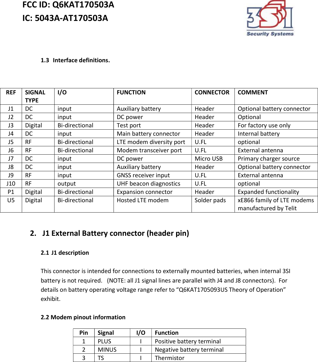
![FCC ID: Q6KAT170503A IC: 5043A-AT170503A 1. Product description 1.1 General AT170503US is a radio product designed by 3SI Security Systems to perform event monitoring and location tracking services. To facilitate the data transfer to 3SI servers, this product has provisions to host a wide range of LTE modems. The following information represents AT170503US integration example with a Telit LTE modem ME866. Other modems may require a layout modification (limited to U5 area only). NOTE: only FCC and/or IC certified modems shall be used for the purpose of integration with AT170503US. 1.2 Sub-sections AT170503US contains the following sub-sections: Please refer to Q6KAT170503US Block Diagram exhibit for more information. Sub-section TYPE FREQUENCY [MHz] COMMENT GNSS receiver 1559 – 1610 WiFi transceiver 2412 - 2462 Beacon transceiver 2402 - 2480 Bluetooth Beacon transmitter 216.475 UHF Battery charger charger N/A Optional use Processor system logic 40](https://usermanual.wiki/3Si-Security-Systems/AT170503A/User-Guide-3728135-Page-2.png)
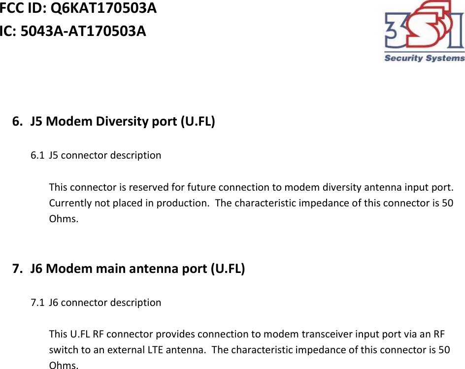
![FCC ID: Q6KAT170503A IC: 5043A-AT170503A 14. Integration procedure - Select a xE866 Telit modem that covers desired LTE bands o the modem must be FCC and/or IC approved - Add the modem as U5 to AT170503US schematic - Perform on-board antenna optimization for the desired frequency range o Antenna geometry (if required) o Matching network (if required) - Perform EMC evaluation to validate continued FCC and IC compliance 15. Product labeling - Place on the product the label with the following content: CONTAINS: FCC ID: Q6KAT170503A, [MODEM FCC ID] IC: 5043A-AT170503A, [MODEM IC ID] 16. Tune Up Information The module tuning is performed during the manufacturing process. The integrated product requires no further tuning. The user cannot access nor alter any tuning parameters.](https://usermanual.wiki/3Si-Security-Systems/AT170503A/User-Guide-3728135-Page-13.png)