3Si Security Systems AT170503A Asset Tracker User Manual
3Si Security Systems Inc. Asset Tracker
User manual

FCC ID: Q6KAT170503A
IC: 5043A-AT170503A
AT170503US Integration Manual
REGULATORY NOTICES
FCC
This device complies with the RF safety requirements as per FCC Part 1.1310, RF Exposure radiation limits
for the General Population / Uncontrolled Exposure.
This device shall be installed to maintain a separation distance of 20 cm from the general population.
This device complies with part 15 of the FCC Rules. Operation is subject to the following two conditions:
(1) This device may not cause harmful interference, and (2) this device must accept any interference
received, including interference that may cause undesired operation.
Any changes or modifications not expressly approved by 3SI Security Systems could void the user's
authority to operate the equipment.
INDUSTRY CANADA
This device complies with the RF safety requirements for Canada as per RSS-102, RF Exposure radiation
limits for the General Population / Uncontrolled Exposure.
Cet appareil est conforme aux exigences de sécurité RF pour le Canada selon RSS-102, Limites de
rayonnement RF d'exposition pour la population générale / exposition incontrôlée.
This device shall be installed to maintain a separation distance of 20 cm from the general population.
Cet appareil doit être installé pour maintenir une distance de séparation de 20 cm par rapport à la
population générale.
This device complies with Industry Canada’s licence-exempt RSSs. Operation is subject to the following two
conditions:
(1) This device may not cause interference; and
(2) This device must accept any interference, including interference that may cause undesired operation of
the device.
Cet appareil est conforme aux RSS exempts de licence d'Industrie Canada. L'opération est soumise aux deux
conditions suivantes:
(1) Cet appareil ne doit pas causer d'interférences; et
(2) Cet appareil doit accepter toute interférence, y compris les interférences susceptibles de provoquer un
fonctionnement indésirable de l'appareil.
FCC ID: Q6KAT170503A
IC: 5043A-AT170503A
1. Product description
1.1 General
AT170503US is a radio product designed by 3SI Security Systems to perform event monitoring
and location tracking services. To facilitate the data transfer to 3SI servers, this product has
provisions to host a wide range of LTE modems. The following information represents
AT170503US integration example with a Telit LTE modem ME866. Other modems may require a
layout modification (limited to U5 area only).
NOTE: only FCC and/or IC certified modems shall be used for the purpose of integration with
AT170503US.
1.2 Sub-sections
AT170503US contains the following sub-sections:
Please refer to Q6KAT170503US Block Diagram exhibit for more information.
Sub
-
section
TYPE
FREQUENCY
[MHz]
COMMENT
GNSS
receiver
1559
–
1610
WiFi
transceiver
2412
-
2462
Beacon
transceiver
2402
-
2480
Bluetooth
Beacon
transmitter
216.475
UHF
Ba
ttery charger
charger
N/A
Optional use
Processor
system logic
40
FCC ID: Q6KAT170503A
IC: 5043A-AT170503A
1.3 Interface definitions.
2. J1 External Battery connector (header pin)
2.1 J1 description
This connector is intended for connections to externally mounted batteries, when internal 3SI
battery is not required. (NOTE: all J1 signal lines are parallel with J4 and J8 connectors). For
details on battery operating voltage range refer to “Q6KAT1705093US Theory of Operation”
exhibit.
2.2 Modem pinout information
Pin
Signal
I/O
Function
1
PLUS
I
Positive battery terminal
2
MINUS
I
Negative battery terminal
3
TS
I
Thermistor
REF
SIGNAL
TYPE
I/O
FUNCTION
CONNECTOR
COMMENT
J1
DC
input
Auxiliary battery
H
eader
Optional battery connector
J2
DC
input
DC power
Header
Optional
J3
Digital
Bi
-
directional
Test port
Header
For factory use only
J4
DC
input
Main battery connector
Header
Internal battery
J5
RF
Bi
-
directional
LTE modem diversity port
U.FL
optional
J6
RF
Bi
-
directional
Modem transceiver port
U.FL
External antenna
J7
DC
input
DC power
Micro USB
Primary charger source
J8
DC
input
Auxiliary battery
Header
Optional battery connector
J9
RF
input
GNSS receiver input
U.FL
External antenna
J10
RF
outp
ut
UHF beacon diagnostics
U.FL
optional
P1
Digital
Bi
-
directional
Expansion connector
Header
Expanded functionality
U5
Digital
Bi
-
directional
Hosted LTE modem
Solder pads
x
E
866
family of LTE modems
manufactured by Telit
FCC ID: Q6KAT170503A
IC: 5043A-AT170503A
3. J2 DC Power Connector (header pin)
3.1 J2 description
This connector is intended for optional connection to external battery charger power sources
when connection through J7 is not required. The J2 signal lines are parallel with J7 lines.
3.2 J2 pinout information
Pin
Signal
I/O
Function
1
P
VBUS
I
Positive
DC source
terminal
2
GND
I
Negative
DC source
terminal
4. J3 Test Port (Hirose 14-pin female)
4.1 J3 Description
This port is used for factory test and diagnostic purposes only. Integrators or users do not
require to access this port.
5. J4 Internal Battery connector (knife contacts)
5.1 J4 connector description
This connector provides connection to the internally mounted battery. The J4 signal lines are
parallel with J1 and J8 lines.
5.2 J4 pinout information (NOTE: all J8 signal lines are parallel to J1 and J8 connectors)
P
in
S
ignal
I/O
F
unction
1
PLUS
I
Positive battery terminal
2
MINUS
I
Negative battery terminal
3
TS
I
Thermistor

FCC ID: Q6KAT170503A
IC: 5043A-AT170503A
6. J5 Modem Diversity port (U.FL)
6.1 J5 connector description
This connector is reserved for future connection to modem diversity antenna input port.
Currently not placed in production. The characteristic impedance of this connector is 50
Ohms.
7. J6 Modem main antenna port (U.FL)
7.1 J6 connector description
This U.FL RF connector provides connection to modem transceiver input port via an RF
switch to an external LTE antenna. The characteristic impedance of this connector is 50
Ohms.
FCC ID: Q6KAT170503A
IC: 5043A-AT170503A
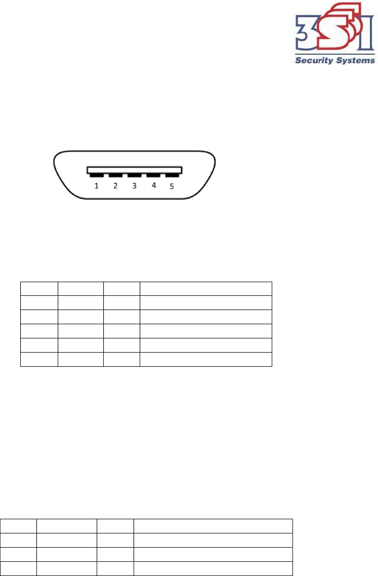
8. J7 DC power connector (micro USB)
8.1 J7 connector pin arrangement
8.2 J7 pinout information
9. J8 auxiliary battery connector (header, 3 pin)
9.1 J8 connector description
J8 connector is designed be optionally placed to connect an auxiliary battery to this radio
product.
9.2 J8 pinout information (NOTE: all J8 signal lines are parallel to J1 and J4 connectors)
P
in
S
ignal
I/O
F
unction
1
PLUS
I
Positive battery terminal
2
MINUS
I
Negative battery terminal
3
TS
I
Thermis
tor
10. J9 GNSS input connector (U.FL)
10.1 J9 connector description
This connector allows attachment of an external GNSS active (i.e. amplified) antenna to the
AT170503US product. The expected range of incoming signals is 1559 – 1610 MHz. This
connector is rated for 50 Ohms characteristic impedance.
Pin
Signal
I/O
Function
1
VBUS
I
Power for charger
2
N/C
-
NOT CONNECTED
3
N/C
-
NOT CONNECTED
4
N/C
-
NOT CONNECTED
5
GND
I
G
round
FCC ID: Q6KAT170503A
IC: 5043A-AT170503A
11. J10 beacon output connector (U.FL)
11.1 J10 connector description
J10 connector is intended to be used during the test and/or development phase and is
normally not installed in production.
12. P1 expansion connector (header, 14 positions)
12.1 P1 connector description
This port enables the system functionality expansion through addition of auxiliary sensors or
actuators.
12.2 P1 connector pinout information
Pin
Signal
I/O
Function
1
GND
I
Ground
2
VBAT
I
Battery power fro
m expansion module
3
EXP
-
INT
I
Expansion module interrupt
4
EXP
-
SPI
-
CLK
I/O
Expansion module generic interface control signal
5
EXP
-
ENABLE
O
Expansion module Enable signal
6
EXP
-
SPI
-
MISO
I/O
Expansion module generic interface control signal
7
V1.8_u
P
O
1.8V IO power from device to Expansion module
8
EXP
-
SPI
-
MOSI
I/O
Expansion module generic interface control signal
9
EXP
-
I2C
-
SDA
I/O
Expansion module generic interface control signal
10
EXP
-
SPI
-
CS
I/O
Expansion module generic interface control sig
nal
11
EXP
-
I2C
-
SCL
I/O
Expansion module generic interface control signal
12
EXP
-
BATT
-
TS
O
Expansion module battery thermistor signal
13
VBAT
I
Battery power from expansion module
14
GND
I
Ground
13. U5 modem hosting socket (solder pads)
13.1 U5 description
U5 pad grid was designed to host LTE M2M xE866 modem family manufactured by Telit.
The modem selection is driven by the type of LTE network to support i.e. Verizon or AT&T.
All modems belonging to xE866 family share the same pinout and can be placed directly on
the reserved solder pads.
Other types of modems may require layout modifications (U5 area only).
FCC ID: Q6KAT170503A
IC: 5043A-AT170503A
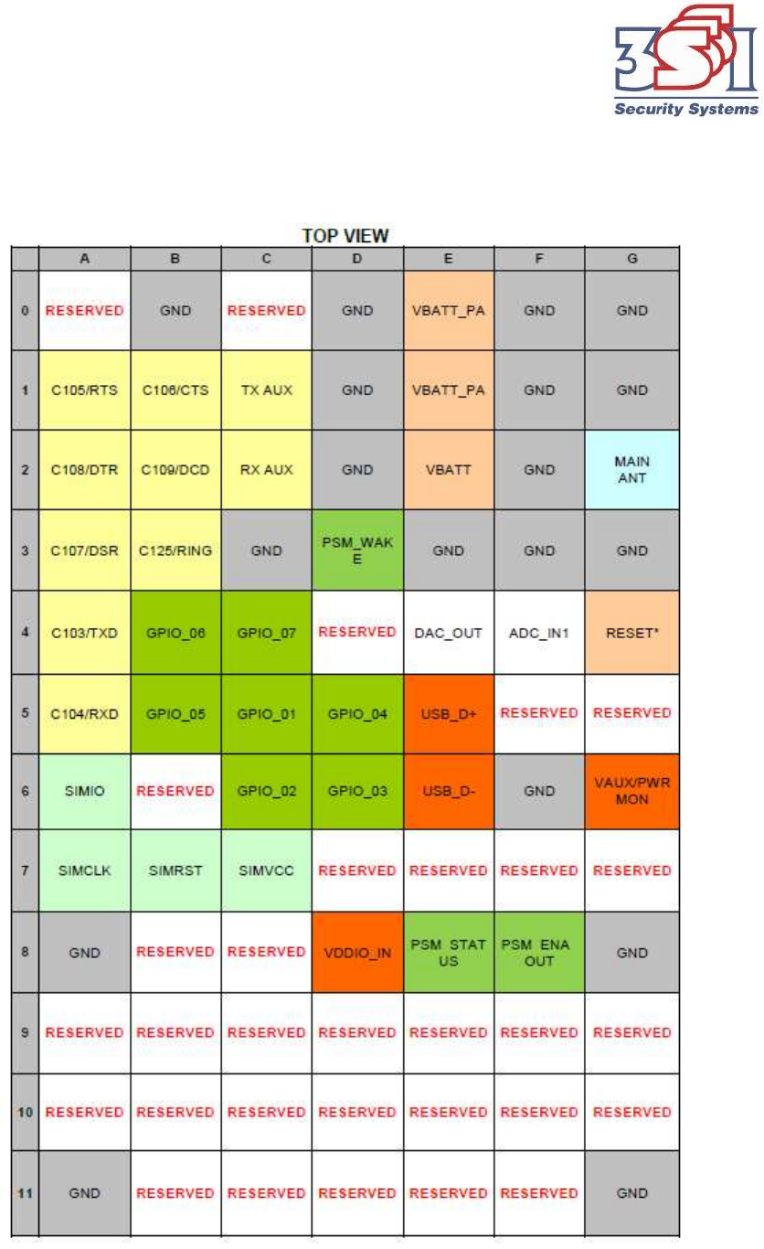
13.2 U5 modem pin grid layout
FCC ID: Q6KAT170503A
IC: 5043A-AT170503A
13.3 U5 modem pinout information
13.3.1 USB HS 2.0 communications port
Pin
Signal
I/O
Function
Comment
E5 USB_D+ I/O USB differential Data (+)
NOT CONNECTED
E6 USB_D- I/O USB differential Data (-)
NOT CONNECTED
13.3.2 Asynchronous Serial Port (USIF0) - Data + HW Flow Control
Pin
Signal
I/O
Function
Type
A4 C103/TXD I Serial data input (TXD) from
DTE
CMOS 1.8V
A5
C104/R
XD
O
Serial data output to DTE
CMOS 1.8V
A2
C108/DTR
I
Input for (DTR) from DTE
CMOS 1.8V
A1 C105/RTS I Input for Request to send
signal (RTS) from DTE
CMOS 1.8V
B1 C106/CTS O Output for Clear to send
signal (CTS) to DTE
CMOS 1.8V
B2 C109/DCD O Output for (DCD) to DTE
NOT CONNECTED
CMOS 1.8V
A3 C107/DSR O Output for (DSR) to DTE
NOT CONNECTED
CMOS 1.8V
B3
C125/RING
O
Output for Ring (RI) to DTE
CMOS 1.8V
13.3.3 Asynchronous Auxiliary Serial Port (USIF1)
Pin
Signal
I/O
Function
Ty
pe
C1 TX_AUX O Auxiliary UART (TX Data to
DTE)
NOT CONNECTED
CMOS 1.8V
C2 RX_AUX I Auxiliary UART (RX Data
from DTE)
NOT CONNECTED
CMOS 1.8V
FCC ID: Q6KAT170503A
IC: 5043A-AT170503A
13.3.4 SIM card interface
Pin
Signal
I/O
Function
Type
C7
SIMVCC - External SIM signal – Power supply for the
SIM
1.8V Only
B7
SIMRST
O
External SIM signal
–
Reset
CMOS 1.8
A7
SIMCLK
O
External SIM signal
–
Clock
CMOS 1.8
A6
SIMIO
I/O
External SIM signal
–
Data I/O
CMOS 1.8
X
SIMIN
I
Presence SIM input
CMOS 1.8
13.3.5 Digital I/O
Pin
Signal
I/O
Function
Type
C5 GPIO_01
SIM_IN
I/O INT Main Function: GPIO01 Configurable
GPIO Alternate Function: SIM_IN
NOT CONNECTED
CMOS 1.8V
C6 GPIO_02
SIM_IN
I/O INT Main Function: GPIO02 Configurable
GPIO Alternate Function: SIM_IN
NOT CONNECTED
CMOS 1.8V
D6 GPIO_03
SIM_IN
I/O INT General Purpose IO Alternate Function:
SIM_IN
NOT CONNECTED
CMOS 1.8V
D5 GPIO_04
SIM_IN
I/O INT Main Function: GPIO04 Configurable
GPIO Alternate Function: SIM_IN
ANT
-
SELECT
-
EXT/INT#
CMOS 1.8V
B5 GPIO_05
SIM_IN
I/O INT Main Function: GPIO05 Configurable
GPIO Alternate Function 1: SIM_IN
NOT CURRENTLY USED
CMOS 1.8V
B4 GPIO_06
ALARM SIM_IN
I/O INT Main Function: GPIO06 Configurable
GPIO Alternate Function 1: ALARM
Alternate Function 2: SIM_IN
NOT CONNECTED
CMOS 1.8V
C4 GPIO_07
STAT_LED
SIM_IN
I/O INT Main Function: GPIO07 Configurable
GPIO Alternate Function 1: STATLED
Alternate Function 2: SIM_IN
NOT CONNECTED
CMOS 1.8V
D8
VDDIO_IN
I
IO bus Supply input
Power
13.3.6 ADC and DAC
Pin
Signal
I/O
Functio
n
Type
F4 ADC_IN1 AI Analog/Digital converter input
NOT CONNECTED
A/D
E4 DAC_OUT AO Digital/Analog converter output
NOT CONNECTED
D/A
FCC ID: Q6KAT170503A
IC: 5043A-AT170503A
13.3.7 RF
Pin
Signal
I/O
Function
Type
G2
MAIN_ANT
I/O
LTE Main Antenna (50 ohm)
RF
13.3.8 Miscellaneous Functions
Pin
Signal
I/O
Function
Type
G4
RESET*
I
Reset Input
VBATT
G6 VAUX
PWRMON
O 1.8V stabilized output
Power ON monitor
Power
D3
PSM_WAKE
I
PSM Wake Up
Analog
E8
PSM_STATUS
O
PSM Status
CMOS 1.8V
F8
PSM_ENA_OUT
O
NOT CONNECTED
CMOS 1
.8V
13.3.9 Power Supply
Pin
Signal
I/O
Function
Type
E2
VBATT
-
Main power supply
(Baseband)
Power
E0 VBATT_PA - Main power supply (Radio
PA)
Power
E1 VBATT_PA - Main power supply (Radio
PA)
Power
B0
GND
-
Ground
Power
D0
GND
-
Ground
Power
F0
GND
-
Ground
Power
G0
GND
-
Ground
Power
D1
GND
-
Ground
Power
F1
GND
-
Ground
Power
G1
GND
-
Ground
Power
D2
GND
-
Ground
Power
F2
GND
-
Ground
Power
C3
GND
-
Ground
Power
E3
GND
-
Ground
Power
F3
GND
-
Ground
Power
G3
GND
-
Ground
Power
F6
GND
-
Ground
Power
A8
GND
-
Ground
Power
G8
GND
-
Ground
Power
A11
GND
-
Ground
Power
G11
GND
-
Ground
Power

FCC ID: Q6KAT170503A
IC: 5043A-AT170503A
13.3.10 Reserved
Pin
Signal
I/O
Function
A0
RESERVED
-
NOT CONNECTED
C0
RESERVED
-
NOT CONNECTED
G5
RESERVED
-
Optionally connected to MODEM
-
RING for NE866 PSM mode support
B6
RESERVED
-
NOT CONNECTED
D7
RESERVED
-
NOT CONNECTED
E7
RESERVED
-
NOT CONNECTED
F7
RESERVED
-
NOT CONNECTED
G7
RESERVED
-
NOT CONNECTED
B8
RESE
RVED
-
NOT CONNECTED
C8
RESERVED
-
NOT CONNECTED
A9
RESERVED
-
NOT CONNECTED
B9
RESERVED
-
NOT CONNECTED
C9
RESERVED
-
NOT CONNECTED
D9
RESERVED
-
NOT CONNECTED
E9
RESERVED
-
NOT CONNECTED
F9
RESERVED
-
NOT CONNECTED
G9
RESERVED
-
NOT CONNECTED
A1
0
RESERVED
-
NOT CONNECTED
B10
RESERVED
-
NOT CONNECTED
C10
RESERVED
-
NOT CONNECTED
D10
RESERVED
-
NOT CONNECTED
E10
RESERVED
-
NOT CONNECTED
F10
RESERVED
-
NOT CONNECTED
G10
RESERVED
-
NOT CONNECTED
B11
RESERVED
-
NOT CONNECTED
C11
RESERVED
-
NOT
CONNECTED
D4
RESERVED
-
NOT CONNECTED
F5
RESERVED
-
NOT CONNECTED
F11
RESERVED
-
NOT CONNECTED
E11
RESERVED
-
NOT CONNECTED
D11
RESERVED
-
NOT CONNECTED

FCC ID: Q6KAT170503A
IC: 5043A-AT170503A
14. Integration procedure
- Select a xE866 Telit modem that covers desired LTE bands
o the modem must be FCC and/or IC approved
- Add the modem as U5 to AT170503US schematic
- Perform on-board antenna optimization for the desired frequency range
o Antenna geometry (if required)
o Matching network (if required)
- Perform EMC evaluation to validate continued FCC and IC compliance
15. Product labeling
- Place on the product the label with the following content:
CONTAINS:
FCC ID: Q6KAT170503A, [MODEM FCC ID]
IC: 5043A-AT170503A, [MODEM IC ID]
16. Tune Up Information
The module tuning is performed during the manufacturing process. The integrated product requires no
further tuning. The user cannot access nor alter any tuning parameters.