ALE BTMOD02 Bluetooth module User Manual BTDB user s manual
ALE International Bluetooth module BTDB user s manual
UserManual.wiki
>
ALE
>
BTMOD02 User Manual
User Manual
Navigation menu
Upload a User Manual
Namespaces
Wiki Guide
HTML
PDF
Info
Views
User Manual
Discussion / Help
Navigation
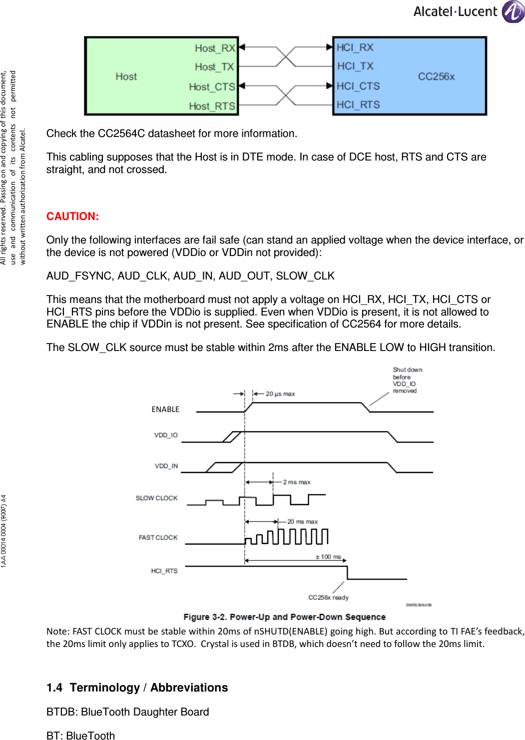
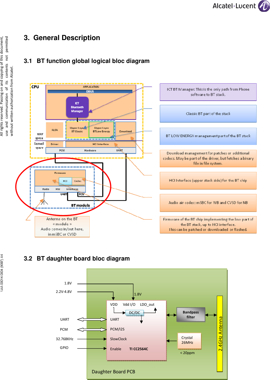
![All rights reserved. Passing on and copying of this document, use and communication of its contents not permitted without written authorization from Alcatel. Generalities 1.1 Introduction 1.1.1 Overview The main objectives for this board, discussed also with the marketing are: • Get lowest cost solution to enable BT for a maximum of IP terminals • Enable new usages like o The phone is seen as a carkit for a smartphone o The phone can exchange phonebook with a smartphone o The phone can support tags through BT Low Energy • From R&D point of view: o The board must be small enough to be integrated easily into our ID. o The board must integrate the antenna to avoid a re-certification for each phone which would use it. For this project, a pre-study has been done. See reference [1]. The choice is to do a daughter board with the chip CC2564C from Texas Instruments, with an integrated antenna on the layout (Printed antenna). This device complies with part 15 of the FCC Rules. Operation is subject to the following two conditions: (1) This device may not cause harmful interference, and (2) this device must accept any interference received, including interference that may cause undesired operation. Please note that changes or modifications not expressly approved by the party responsible for compliance could void the user’s authority to operate the equipment. Note: This equipment has been tested and found to comply with the limits for a Class B digital device, pursuant to part 15 of the FCC Rules. These limits are designed to provide reasonable protection against harmful interference in a residential installation. This equipment generates, uses and can radiate radio frequency energy and, if not installed and used in accordance with the instructions, may cause harmful interference to radio communications. However, there is no guarantee that interference will not occur in a particular installation. If this equipment does cause harmful interference to radio or television reception, which can be determined by turning the equipment off and on, the user is encouraged to try to correct the interference by one or more of the following measures: —Reorient or relocate the receiving antenna. —Increase the separation between the equipment and receiver.](https://usermanual.wiki/ALE/BTMOD02/User-Guide-3367805-Page-2.png)
![All rights reserved. Passing on and copying of this document, use and communication of its contents not permitted without written authorization from Alcatel. LE: Low Energy 1.5 Related Documents Document Reference number Alcatel documents [1] Bluetooth: Pre-study of a low cost solution for BT in Desktop Phones 3AK_29000_0041_BEZZA [2] 8088 Hardware external specification 3AK_29000_0080_EDZZA [3] ESD CSBU R&D - PB Design/Layout rules 8AL 51074 0003 DSZZA [4] NOE3G INDUSTRIAL REQUIREMENTS 3BN 69030 1403 MCASA External documents [5] All TI documents for CC2564 (upload) 3AK_29_CC256X_BLUETOOTH_02278 [6]](https://usermanual.wiki/ALE/BTMOD02/User-Guide-3367805-Page-6.png)
![All rights reserved. Passing on and copying of this document, use and communication of its contents not permitted without written authorization from Alcatel. 2.3 Environmental requirements These are the same as for the terminal for which this board is intended. The tests are made on the daughter board mounted in a final product, so they are part of the product qualification. This BTDB board cannot be co-located with other transmitters. If mount this board on final product, Should add FCC ID and IC information in the product label (FCC ID: OL3BTMOD02, IC: 1737D-BTMOD02). For a host manufacture’s using a certified modular, if (1) the module’s FCC ID is not visible when installed in the host, or (2) if the host is marketed so that end users do not have straightforward commonly used methods for access to remove the module so that the FCC ID of the module is visible; then an additional permanent label referring to the enclosed module: “Contains Transmitter Module FCC ID: OL3BTMOD02, IC: 1737D-BTMOD02” or “Contains FCC ID: OL3BTMOD02, Contains IC: 1737D-BTMOD02” must be used. The host OEM user manual must also contain clear instructions on how end users can find and/or access the module and the FCC ID. This equipment complies with radio frequency exposure limits set forth by the Innovation, Science and Economic Development Canada for an uncontrolled environment. This equipment should be installed and operated with a minimum distance of 15mm between the device and the user or bystanders. This device must not be co-located or operating in conjunction with any other antenna or transmitter. Cet équipement est conforme aux limites d'exposition aux radiofréquences définies par la Innovation, Sciences et Développement économique Canada pour un environnement non contrôlé. Cet équipement doit être installé et utilisé avec un minimum de 15mm de distance entre le dispositif et l'utilisateur ou des tiers. Ce dispositif ne doit pas être utilisé à proximité d’une autre antenne ou d’un autre émetteur. For details see for example the Smart Deskphone 8088 HW external specification (see ref [2])](https://usermanual.wiki/ALE/BTMOD02/User-Guide-3367805-Page-8.png)
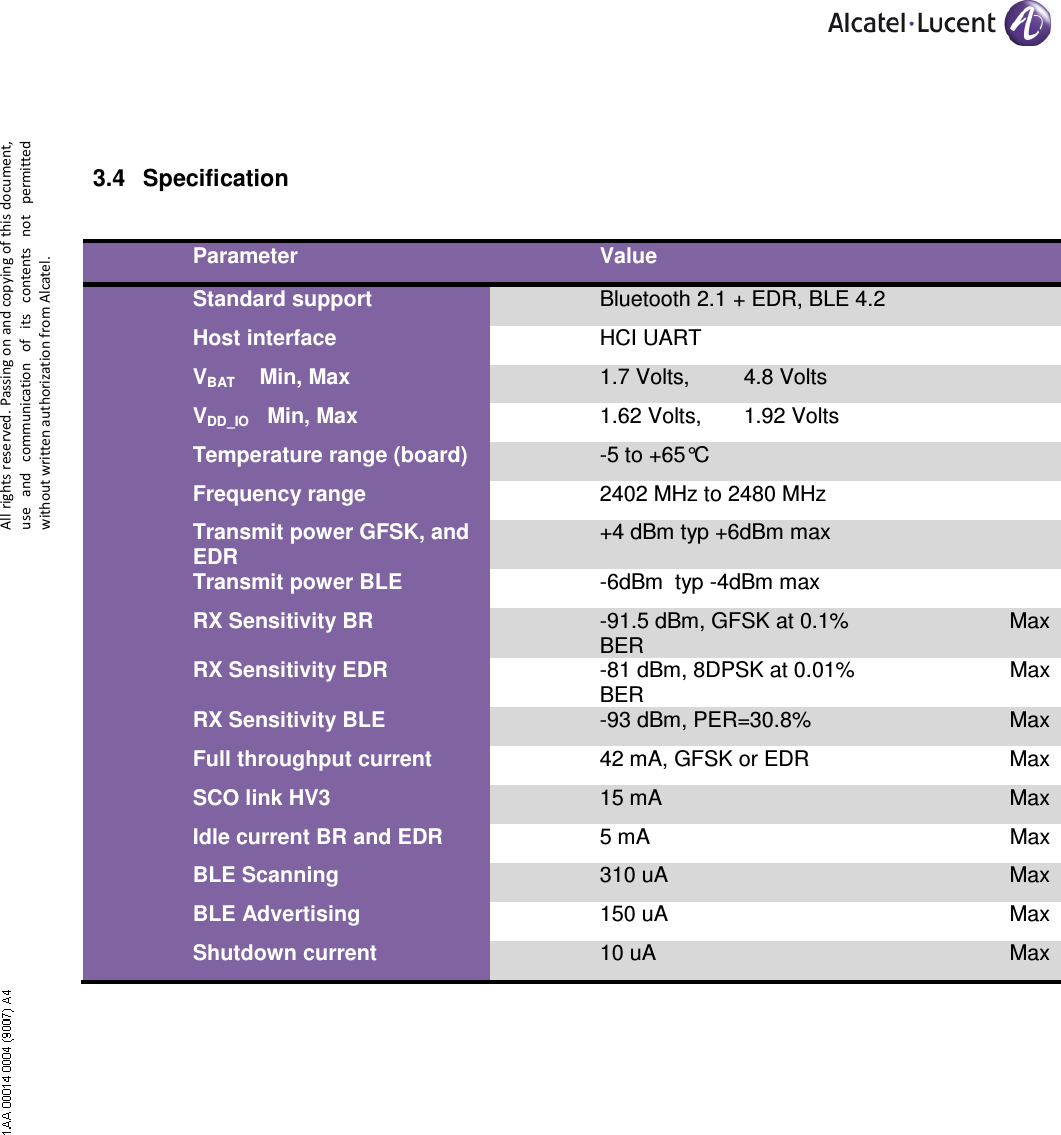

![All rights reserved. Passing on and copying of this document, use and communication of its contents not permitted without written authorization from Alcatel. 4.2 Radiofrequency 4.2.1 Antenna choice Two major types of antennas could be implemented: • Ceramic antenna: very compact, these are easy to mount, but have a cost of around 13 cents. Their performance is medium. • PCB antenna: this uses a track of copper on the PCB. It gives good performance at 2.4GHz, very low cost, but needs more surface and may need some tuning. The PCB antenna designs are well known. The BTDB will use the PCB antenna. In this type, we have for BT two main choices: • The inverted F antenna, well known, good performance, very low dependence to the environment . It has a large bandwidth. Typical size is 26mm x 8mm. This is too large for our module. • The meandered inverted F antenna, which is a variant to have more compacity: 16mm x 6mm. This one is good for our design. This antenna is sensitive to small dimension changes, and has a narrow bandwidth. So an exact copy of the reference dimensions must be done. This antenna is typically used in BT USB dongle designs. The meandered inverted F antenna will be used for the design. Check the following document for the antenna specification and implementation: http://www.ti.com/litv/pdf/swra117d (also available in doc ref [3]). To improve the antenna efficiency, we changed the antenna shape data as the following figure and table: GND move to feed line 0.59mm (D5, L3), cut antenna 0.80mm (L1). The antenna gain is 5.1dBi.](https://usermanual.wiki/ALE/BTMOD02/User-Guide-3367805-Page-14.png)
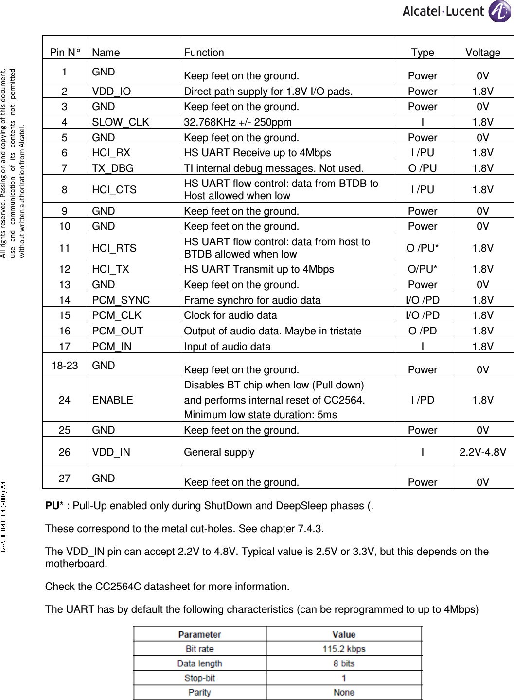
![All rights reserved. Passing on and copying of this document, use and communication of its contents not permitted without written authorization from Alcatel. An 1.8V feed is provided for the I/O. This is not a sensitive supply and no special care is needed for this in terms of noise (the typical noise level found on digital boards on 1.8V is acceptable). 4.3 Layout 4.3.1 BTDB layout The layout recommendations from Texas Instruments must be followed. Refer to document: http://www.ti.com/lit/an/swra420/swra420.pdf (also available in doc ref [3]). The layout MUST be based on the evaluation kit of TI. The main page for this follows: http://processors.wiki.ti.com/index.php/CC256x 4.3.2 Place requirements of BTDB on mainboard To make the BTDB on mainboard has similar antenna resonant frequency as BTDB alone, there are some BTDB place requirements: 1. The under space of the BTDB antenna need to be empty, at least 5.5mm empty space. 2. The right side of BTDB antenna need to be at least 3mm empty space. 3. The left side of BTDB antenna need to be at least 5mm empty space. 4.4 Software A set of patches and features improvements must be downloaded to the CC2564 chip. This is named as “service pack”. It depends on the device version (A, B or C), and MUST be downloaded when the device is powered up, before any RF usage.](https://usermanual.wiki/ALE/BTMOD02/User-Guide-3367805-Page-16.png)
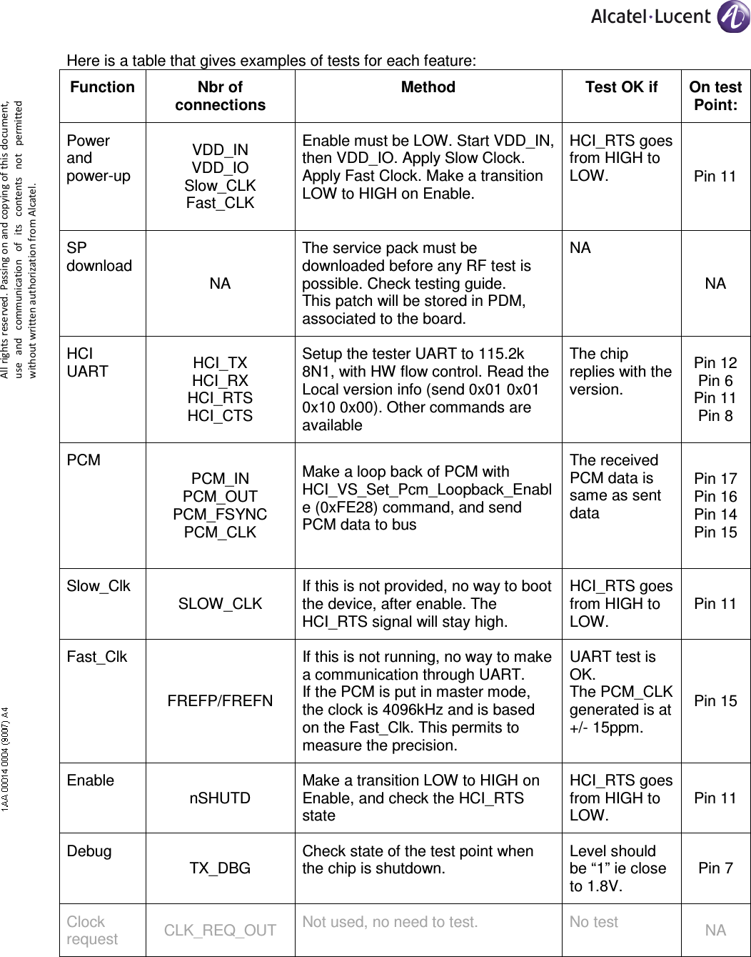
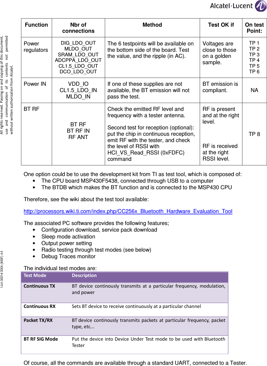
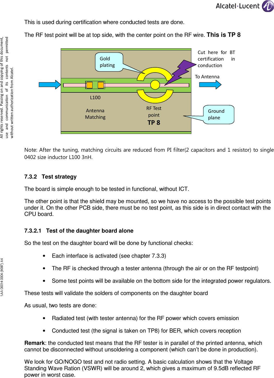
![All rights reserved. Passing on and copying of this document, use and communication of its contents not permitted without written authorization from Alcatel. 5. Thermal management No thermal issue is foreseen for this board, as power levels are low (about 130mW in EDR full throughput). So no special thermal care must be taken. 6. Reliability It can be calculated with CADRE tool according to the reliability database user guide. http://alda.web.alcatel-lucent.com/transition_docs/CADRE_SR332/SR332-CADRE-main.html Usually the calculation is done within the final product (the phone) 7. Industrial Considerations 7.1 Manufacturing Trimming The radio has an auto-calibration feature. This means that once the radio parameters have been defined by engineering, and stored in the chip, there is no need of trimming in manufacturing. During engineering, care must be taken to define the right RF level output taking into account the losses in the bandpass filter and potential impedance adaptation cells. 7.2 Requirements The module is considered as a component for the manufacturing, and must be stores in a reel, in vacuum packing until is mounted on the mother board. Refer to doc: [3] and [4] for more information 7.3 Testability This proposal is based on a discussion with NPI. This may be refined in a second step. 7.3.1 Testpoints There is no need of having one test-point per trace, as the board will not use ICT. The AOI (automatic vision) test is foreseen to be made before the shield is put on the board, but before the soldering. For the RF track to antenna, there will be a pad in series, in order to disconnect the PCB antenna by cutting the track. The pad will then be used to get the RF signal, and the GND surrounding for the shield. See other IP-Phones CPUs for reference.](https://usermanual.wiki/ALE/BTMOD02/User-Guide-3367805-Page-18.png)
![All rights reserved. Passing on and copying of this document, use and communication of its contents not permitted without written authorization from Alcatel. In consequence, the generated RF signal at the tester must be increased to compensate this. The best reliable solution is to take a golden sample of the board to setup the RF level for conducted BER measurement. This will simplify the procedure in manufacturing. Radiated test: RF power (High level signal) Conducted test: BER (low level signal) 7.3.2.2 Test of the daughter board mounted in a phone For the tests of the BTDB on the mother board, we must consider it as a component. • The connections to the BTDB are checked by functional test of the interfaces • The RF is tested through the air. Only the RF radiated test is done to check: • RF power level • BT connection (for example by pairing a device) 7.3.3 Test method Here is an overview of the means to test the connections within the BTDB. The board can be individually tested (no need of mounting it on the CPU). Many functions of the chip can be driven through UART Vendor Specific commands. The list is given in the following document: http://processors.wiki.ti.com/index.php/CC256x_VS_HCI_Commands (also available in doc ref [3]). Some test method can also be taken from the following page: http://processors.wiki.ti.com/index.php/CC256x_Testing_Guide (also available in doc ref [3]). Before any RF is activated, the Service Pack (SP) must be downloaded to the CC2564C. For manufacturing, this ServicePack will be stored in PDM. It may evolve with time, but the manufacturing tools do not need to have the latest version, because the phone software will have it integrated, and download it at phone start-up. Only if there is an identified but which could impact the manufacturing tests, the SP will be updated. Both antenna and tester are connected: mismatch with about 9.5dB reflected power max.](https://usermanual.wiki/ALE/BTMOD02/User-Guide-3367805-Page-20.png)