AMPAK Technology WSDT752BSC BLE SiP User Manual Manual
AMPAK Technology Inc. BLE SiP Manual
Manual

兆福科 Gigafu Technology Inc. http://www.gigafu.com.tw/ Proprietary & Confidential Information
兆福科技股份有限公司
SPECIFICATION
SPEC. NO.: REV: 2.0
DATE: 2018, July.-16
PRODUCT NAME: WSDT-752B_SC
APPROVED CHECKED PREPARED DCC ISSUE
NAME

Gigafu Technology Inc. http://www.gigafu.com.tw/ Proprietary & Confidential Information
GIGAFU
WSDT-752B_SC
ARM Cortex M3 + Bluetooth Low Energy
with Antenna Module
Product Specification Sheet

Gigafu Technology Inc. http://www.gigafu.com.tw/ Proprietary & Confidential Information i
May-14/2018
Revision History
Date Revision Content Revised By
Version
2015/03/31 - Original release R & D 1.0
2015/07/08
- Modify voltages ratings
- Add power consumption
- Replace outline dimension
Ander 1.1
2015/07/08 - Modify RF Specification May 1.2
2015/07/13 - Add Antenna keep out area size
Ander 1.3
2015/09/09 - Update Operating Temperature
- Update Power Consumption Ander 1.4
2015/10/21 - Modify 7.1 schematic Peter 1.5
2015/11/04 - Renamed Peter 1.6
2015/12/30 -
Modify temperature of operation
and storage Peter 1.7
2018/05/14 - Modify General Specification Geoffrey 1.8
2018/07/12 - Add FCC/IC Statement Geoffrey 1.9
2018/07/16 - Add Label Drawing Geoffrey 2.0

Gigafu Technology Inc. http://www.gigafu.com.tw/ Proprietary & Confidential Information ii
May-14/2018
Contents
Revision History........................................................................................................ i
Contents ................................................................................................................... ii
1. Introduction.......................................................................................................... 1
1.1 DESCRIPTION......................................................................................................................1
1.2 APPLICATIONS....................................................................................................................1
2. FEATURES............................................................................................................ 2
3. General Specification .......................................................................................... 4
3.1 General Specification ..........................................................................................................4
3.2 Voltages ...............................................................................................................................4
3.2.1 Absolute Maximum Ratings .......................................................................................4
3.2.2 Recommended Operating Ratings ............................................................................4
3.3 Power Consumption............................................................................................................5
3.3.1 BLE Power Consumption...........................................................................................5
4. Main CPU Overview ............................................................................................. 6
4.1 CM3 Features.......................................................................................................................6
5. RF Specification................................................................................................... 7
5.1 BLE Specification ................................................................................................................7
6. Ceramic Chip Antenna Specification ............................................................... 10
6.1 Description Value .............................................................................................................. 10
7. Pinout Information ............................................................................................. 11
7.1 Schematic Diagram ........................................................................................................... 11
7.2 Pin Descriptions ................................................................................................................ 11
7.3 Pin Number Define.............................................................................................................13
8. Software Overview............................................................................................. 14
8.1 Software tool installation...................................................................................................14
8.2 WSDT-752B_SC board GPIO configuration file path........................................................ 14
8.3 PIN define in header file Board.h ......................................................................................14
9. Module Dimensions ........................................................................................... 15
9.1 Outline Dimension (Unit: mm) ......................................................................................15
9.2 Recommended Footprint (Unit: mm)............................................................................ 18

Gigafu Technology Inc. http://www.gigafu.com.tw/ Proprietary & Confidential Information iii
May-14/2018
10. Recommended Reflow Profile ........................................................................ 19
11. Label Drawing................................................................................................... 20
12. Packing Information ........................................................................................ 21
12.1 Packing Dimension..........................................................................................................21
13.Statement........................................................................................................... 22
13.1 FCC Statement:................................................................................................................ 22
13.2 ISED Statement:...............................................................................................................22
13.3 FCC Label Instructions.................................................................................................... 23

Gigafu Technology Inc. http://www.gigafu.com.tw/ Proprietary & Confidential Information 1
May-14/2018
1. Introduction
GIGAFU Technology would like to announce a low-cost and low-power consumption
module which has of the BLE functionalities. The highly integrated WSDT-752B_SC
with RF front end BLE module makes the possibilities of Bluetooth Low Energy HID
and other applications.
1.1 DESCRIPTION
The WSDT-752B_SC is very low active and low power mode current consumption as
well as fast mode transitions provide excellent battery lifetime and allows operation
on small coin cell batteries and in energy harvesting applications.
Integrated a powerful 32-bit Cortex M3 running at 48 MHz has more than 30% more
processing power per MHz than Cortex M0 based systems and significantly more
than 8 and 16-bit processors.
The Bluetooth Low Energy Controller is embedded into ROM and are partly running
on a separate ARM Cortex M0 dedicated for radio purpose. This improves overall
system performance and power consumption as well as frees up FLASH memory for
the application.
1.2 APPLICATIONS
Consumer electronics
Mobile phone accessories
Sports & Fitness equipment
HID applications
Home Automation and Lighting Control
Alarm and Security
Electronic Shelf Labeling
Proximity Tags
Medical and Healthcare
Remote Controls
Wireless Sensor Networks

Gigafu Technology Inc. http://www.gigafu.com.tw/ Proprietary & Confidential Information 2
May-14/2018
2. FEATURES
Lead Free design which is compliant with RoHS requirements.
Integrated Ceramic Chip Antenna
Integrated Power Inductor 10uH for DC/DC converter
- 2.4 GHz RF transceiver compatible with Bluetooth 4.2 low energy and
proprietary communication protocols
- Programmable GFSK modulation mode.
- Supports data rates between 50 kbps and 5 Mbps
- Programmable output power up to +5 dBm
- Suitable for systems targeting compliance with worldwide radio frequency
regulations
- All Digital Peripheral Pins can be Routed to any GPIO
- 4 General-purpose Timer Modules (8x 16-bit or 4x 32 bit-timer, PWM each)
- 12-bit ADC, 200-ksamples/s, 8 channel analog MUX
- Continuous Time Comparator
- Ultra-low-power analog comparator
- Programmable Current Source
- UART
- SPI
- I2C
- I2S
- 10 GPIO
- True Random Number Generator (TRNG)
- Real-time clock
- AES-128 security module
- Support for 8 capacitive sensing channels
- Integrated Temperature Sensor
- Very few external components
- Low-speed clock can be derived from high-speed crystal
Gigafu Technology Inc. http://www.gigafu.com.tw/ Proprietary & Confidential Information 3
May-14/2018
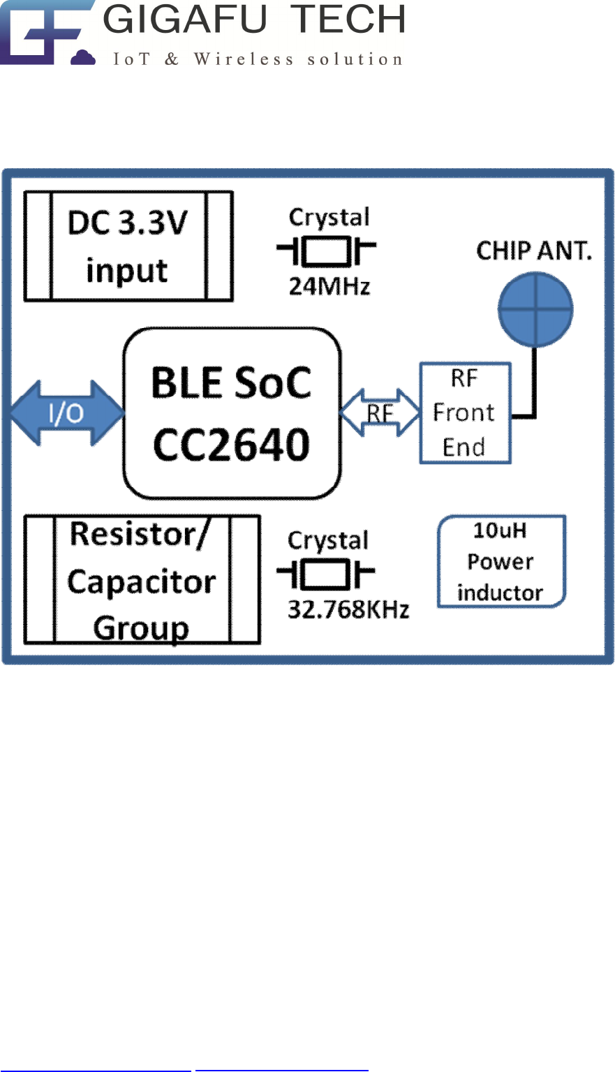
System Block Diagram
Gigafu Technology Inc. http://www.gigafu.com.tw/ Proprietary & Confidential Information 4
May-14/2018
3. General Specification
3.1 General Specification
3.2 Voltages
3.2.1 Absolute Maximum Ratings
Symbol Description Min. Max. Unit
VDDS Module Voltage -0.2 4.0 V
VDDS2 Module Voltage -0.2 4.0 V
VDDS_DCDC Module Voltage -0.2 4.0 V
3.2.2 Recommended Operating Ratings
Test conditions: At room temperature 25°C
Symbol Min. Typ. Max. Unit
VDD 2.16 3.3 3.465 V
Model Name WSDT-752B_SC
Product Description BLE module
Dimension 10.0 mm x 10.0 mm x 1.5 mm (W*L*T)
Operating temperature -10°C to +65°C
Storage temperature -20°C to +85°C
Humidity Operating Humidity 10% to 80% Non-Condensing
Storage Humid
ity 5% to 95% (Non
-
Condensing)
Weight 0.023 g +/- 10g
Gigafu Technology Inc. http://www.gigafu.com.tw/ Proprietary & Confidential Information 5
May-14/2018
3.3 Power Consumption
3.3.1 BLE Power Consumption
Test conditions: TX mode @VDD=3.3V; Temp=25°C
Current@VDD
Test at 25℃/3.3V (Default FW@ROM)
Power Mode Description Current
(Peak )
Initialize DUT link to Smart RF Studio 2.7mA
Tx Continuous
Transmit Packet Continously@1.82dBm
8.1mA
Rx Continuous
Receive Packet Continuously 7.2mA
Tx Packet Transmit Packet to Golden Sample 3.5mA
RX Packet Receive Packet From Golden Sample 7.5mA
238uA
Broadcast
After Press Reset Button ,enter
advertising state for 10 sec then enter
Standby Mode(Specific FW)
10uA
1.4uA (Typical)
Deep Sleep mode (timer on)
3.3V Typ. Max. Unit
Broadcast -- 238 uA
Srandby Mode 1.4 10 uA

Gigafu Technology Inc. http://www.gigafu.com.tw/ Proprietary & Confidential Information 6
May-14/2018
4. Main CPU Overview
The WSDT-752B_SC contains an ARM® Cortex™ M3 (CM3) 32-bit CPU, which runs
the application and protocol stack in the product, and the protocol stack in the
wireless network processor (WNP) products.
4.1 CM3 Features
32-bit ARM Cortex-M3 architecture optimized for small-footprint embedded
applications
Outstanding processing performance combined with fast interrupt handling
Thumb®-2 mixed 16- and 32-bit instruction set delivers the high performance
expected of a 32-bit ARM core in a compact memory size usually associated
with 8- and 16-bit devices, typically in the range of a few kilobytes of memory
for microcontroller-class applications:
–Atomic bit manipulation (bit-banding), delivering maximum memory use and
streamlined peripheral control
–Unaligned data access, enabling data to be efficiently packed into memory
Fast code execution permits slower processor clock or increases sleep mode
time
Harvard architecture characterized by separate buses for instruction and data
Efficient process core, system and memories
Hardware division and fast digital-signal-processing oriented multiply
accumulate
Saturating arithmetic for signal processing
Deterministic, high-performance interrupt handling for time-critical
applications
Enhanced system debug with extensive breakpoint and trace capabilities
Serial wire trace reduce the number of pins required for debugging and
tracing
Migration from the ARM7™ processor family for better performance and
power efficiency
Optimized for single-cycle flash memory use
Ultra-low power consumption with integrated sleep modes
48 MHz operation – the operating frequency can be dynamically altered to
minimize power requirements.
1.25 DMIPS / MHz
Gigafu Technology Inc. http://www.gigafu.com.tw/ Proprietary & Confidential Information 7
May-14/2018
5. RF Specification
5.1 BLE Specification
1 Mbps GFSK (Bluetooth low energy)
Conditions : VDD=3.3V ; Temp:25°C. Using Anisu CombiTest with MT8852B
TX
Output Power
TX PARAMETER limit MIN TYP MAX UNIT
Output power
@2402MHz
>-20
<+10 0.92 2.4 dBm
Peak to Average Power
@2402MHz <3dB 0.14 dB
Output power
@2440MHz
>-20
<+10 0.74 dBm
Peak to Average Power
@2440MHz <3dB 0.13 dB
Output power
@2480MHz
>-20
<+10 0.39 dBm
Peak to Average Power
@2480MHz <3dB 0.14 dB
Carrier Frequency Offset and Drift
TX PARAMETER limit MIN TYP MAX UNIT
Frequency Offset
@2402MHz ≦±150 kHz
-0.9 5.7 10.6 KHz
Drift Rate / 50 µs
@2402MHz
≦
20 kHz / 50
µs 10.65 KHz
Max Drift
@2402MHz ≦50 kHz -10 KHz
Frequency Offset
@2440MHz ≦±150 kHz
2.5 6.5 9.9 KHz
Drift Rate / 50 µs
@2440MHz
≦
20 kHz / 50
µs -7.37 KHz
Max Drift
@2440MHz ≦50 kHz -7 KHz
Frequency Offset
@2480MHz ≦±150 kHz
-0.2 5.1 7.1 KHz

Gigafu Technology Inc. http://www.gigafu.com.tw/ Proprietary & Confidential Information 8
May-14/2018
Drift Rate / 50 µs
@2480MHz
≦
20 kHz / 50
µs -8.85 KHz
Max Drift
@2480MHz ≦50 kHz -11 KHz
Modulation Characteristics
TX PARAMETER limit MIN TYP MAX UNIT
F1avg
@2402MHz
225 kHz <
F1avg < 275
kHz
252 263 KHz
F2max
@2402MHz >= 185 kHz
201 KHz
'F2max' Pass Rate
@2402MHz > 99.9 % 100 %
F1/F2 ratio
@2402MHz >= 0.80 20
F1avg
@2440MHz
225 kHz <
F1avg < 275
kHz
261.2 271.4 KHz
F2max
@2440MHz >= 185 kHz
214.4 KHz
'F2max' Pass Rate
@2440MHz > 99.9 % 100 %
F1/F2 ratio
@2440MHz >= 0.80 20
F1avg
@2480MHz
225 kHz <
F1avg < 275
kHz
262 273.7 KHz
F2max
@2480MHz >= 185 kHz
210 KHz
'F2max' Pass Rate
@2480MHz > 99.9 % 100 %
F1/F2 ratio
@2480MHz >= 0.80 20
Gigafu Technology Inc. http://www.gigafu.com.tw/ Proprietary & Confidential Information 9
May-14/2018
RX
Receiver sensitivity(Power Level: -90.0 dBm, Dirty Tx Status: On)
RX PARAMETER limit MIN TYP MAX UNIT
Frame Error
Rate@2402MHz <= 30.800 %
12.6 %
Frame Error
Rate@2440MHz <= 30.800 %
21.07 %
Frame Error Rater
@2480MHz <= 30.800 %
14.74 %
PER Report Integrity(Power Level: -30.0 dBm, Packet Number Mode: Random)
RX PARAMETER limit MIN TYP MAX UNIT
Frame Error
Rate@2402MHz
50.0 % <=
PER <= 65.4
%
50.4
%
Frame Error
Rate@2440MHz
50.0 % <=
PER <= 65.4
%
50.4
%
Frame Error
Rate@2480MHz
50.0 % <=
PER <= 65.4
%
50.3
%
Maximum Input Signal Level(Power Level: -10.0 dBm)
RX PARAMETER limit MIN TYP MAX UNIT
Fame Error Rate
@2402MHz
<= 30.800 %
0.8 %
Frame Error
Rate@2440MHz
<= 30.800 %
0.8 %
Frame Error
Rate@2480MHz
<= 30.800 %
0.733 %

Gigafu Technology Inc. http://www.gigafu.com.tw/ Proprietary & Confidential Information 10
May-14/2018
6. Ceramic Chip Antenna Specification
6.1 Description Value
DESCRIPTION VALUE
Working Frequency 2.45 GHz
Bandwidth 170 MHz ( Typ. )
VSWR 2.0 (Max.)
Polarization Linear
Azimuth Beamwidth Omni-directional
Peak Gain 5.88 dBi (Typ.)
Impedance 50 Ω
Maximum Power 1 W
Termination Ni / Sn (Environmentally-Friendly Leadless)
Gigafu Technology Inc. http://www.gigafu.com.tw/ Proprietary & Confidential Information 11
May-14/2018
7. Pinout Information
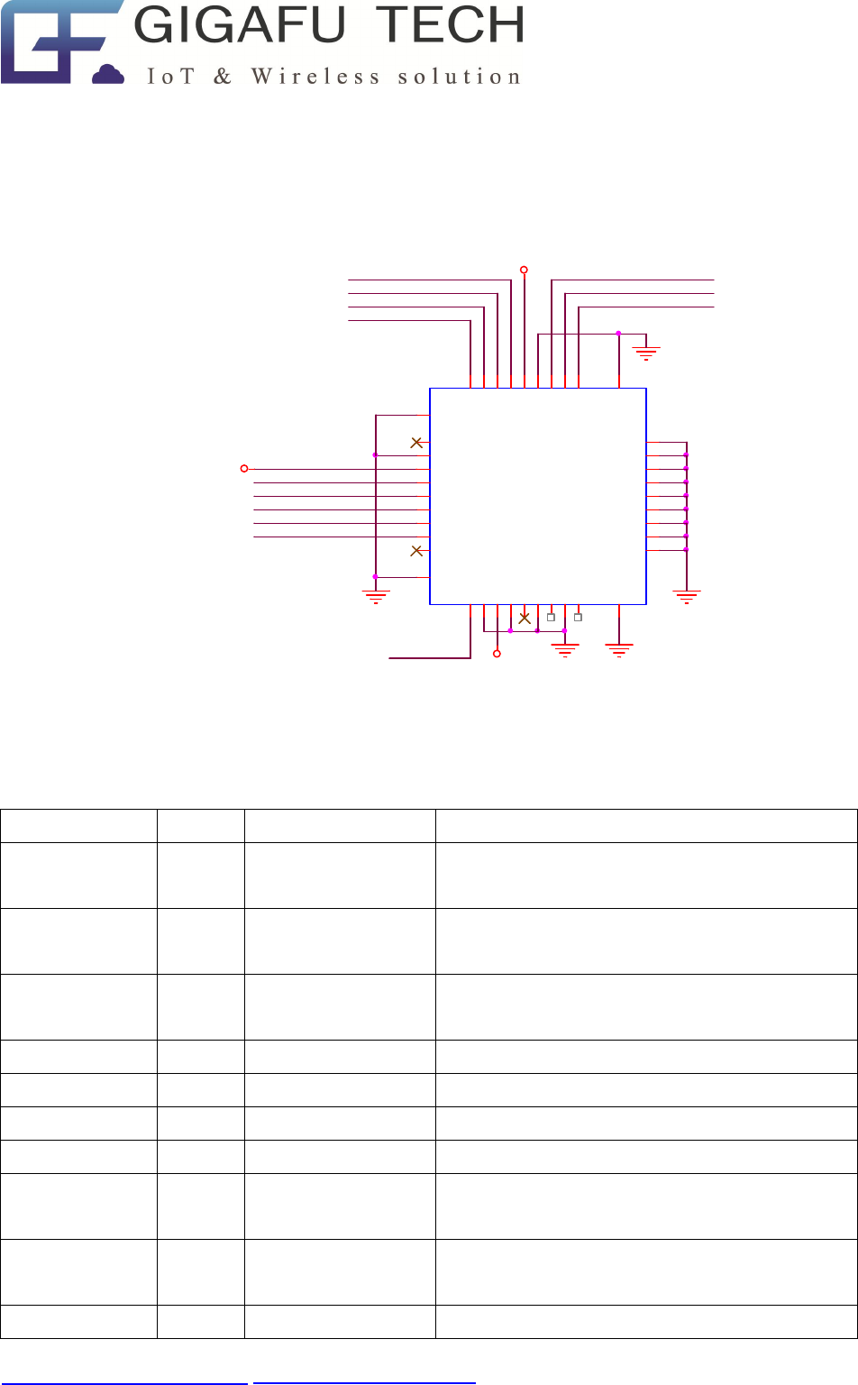
7.1 Schematic Diagram
U1
DIO_0 1
DIO_1 2
DIO_2 3
GND 4
VDDS2 5
JTAG_TMS 6
JTAG_TCK 7
DIO_3 8
DIO_4 9
NC
10
GND
11
VDDS_DCDC
12
nRESET
13
DIO_5
14
DIO_6
15
DIO_7
16
DIO_8
17
NC
18
DIO_9
19
GND
20
VDDS
21
GND
22
NC
23
GND
24
VDDR
25
GND
26
ANT_SMA
27
GND
28 GND 29
GND
30
GND
31
H1 H1
H2 H2
H3 H3
H4 H4
H5 H5
H6 H6
H7 H7
H8 H8
H9 H9
DIO_2
DIO_1
VDDS2
DIO_3/JTAG_TDO
JTAG_TMS
DIO_4/JTAG_TDI
JTAG_TCK
VDDS_DCDC
DIO_8
DIO_6
DIO_5
nRESET
VDDS
DIO_9
DIO_7
DIO_0
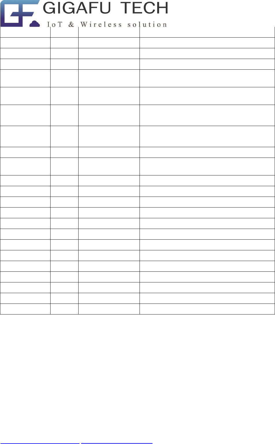
7.2 Pin Descriptions
PIN NAME
PIN
PIN TYPE DESCRIPTION
DIO_0 1 Digital I/O GPIO, ULP Sensor Interface, LED driving
capability , 2mA / 4mA / 8mA
DIO_1 2 Digital I/O GPIO, ULP Sensor Interface, LED driving
capability , 2mA / 4mA / 8mA , UART_TX
DIO_2 3 Digital I/O GPIO, ULP Sensor Interface, LED driving
capability , 2mA / 4mA / 8mA , UART_RX
GND 4 Power Ground
VDDS2 5 Power 3.3V DIO supply
JTAG_TMSC
6 Digital I/O JTAG TMSC
JTAG_TCKC
7 Digital I/O JTAG TCKC
DIO_3 8 Digital I/O JTAG_TDO , High drive capability , 2mA /
4mA / 8mA
DIO_4 9 Digital I/O JTAG_TDI , High drive capability , 2mA /
4mA / 8mA
NC 10 No Connector
Gigafu Technology Inc. http://www.gigafu.com.tw/ Proprietary & Confidential Information 12
May-14/2018
GND 11 Power Ground
VDDS_DCDC 12 Power 3.3V DC/DC supply.
RESET_N 13 Digital input Reset, active-low. No internal pull-up
DIO_5 14 Digital/Analog I/O
GPIO, ULP Sensor Interface, Analog
DIO_6 15 Digital/Analog I/O
GPIO, ULP Sensor Interface, Analog
DIO_7 16 Digital/Analog I/O
GPIO, ULP Sensor Interface, Analog /
I2C_SCL
DIO_8 17 Digital/Analog I/O
GPIO, ULP Sensor Interface, Analog /
I2C_SDA
NC 18 No Connector
DIO_9 19 Digital/Analog I/O
GPIO, ULP Sensor Interface, Analog
GND 20 Power Ground
VDDS 21 Power 3.3V main chip supply
GND 22 Power Ground
NC 23 No Connector
GND 24 Power Ground
NC 25 No Connector
GND 26 Power Ground
NC 27 No Connector
GND 28 Power Ground
GND 29 Power Ground
GND 30 Power Ground
GND 31 Power Ground
GND H1~H9
Power Ground
Gigafu Technology Inc. http://www.gigafu.com.tw/ Proprietary & Confidential Information 13
May-14/2018
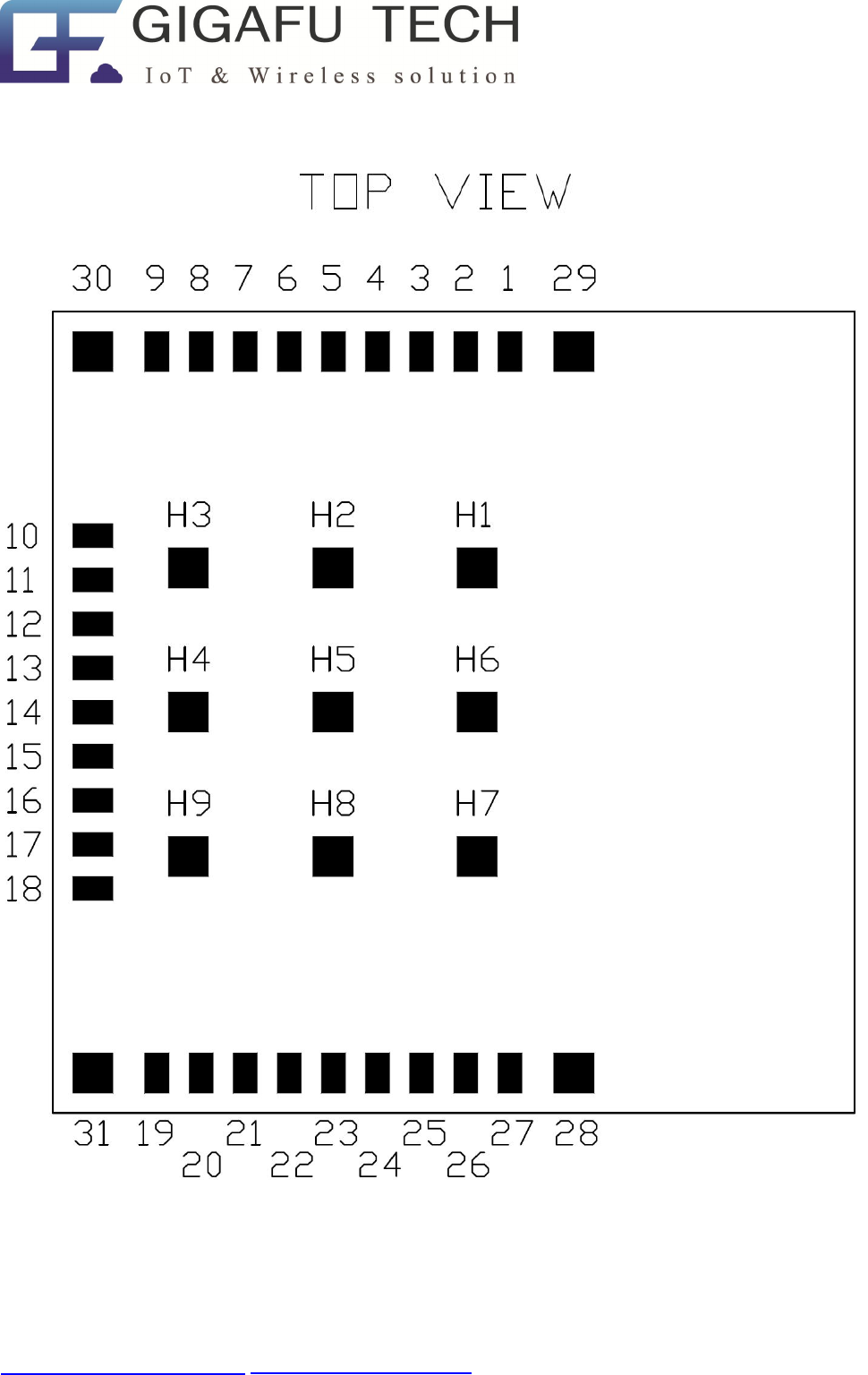
7.3 Pin Number Define

Gigafu Technology Inc. http://www.gigafu.com.tw/ Proprietary & Confidential Information 14
May-14/2018
8. Software Overview
8.1 Software tool installation
Follow TI document “CC2640 BLE Software Developer's Guide” to setup compiler tool,
BSP and related tools.
8.2 WSDT-752B_SC board GPIO configuration file path
...\Projects\ble\common\cc26xx\boards\WSDT-752B_SC
Source files:
...\CC2640EM_4XS\board.h
...\CC2640EM_4XS\board.c
8.3 PIN define in header file Board.h
// UART Board
#define Board_UART_TX IOID_1
#define Board_UART_RX IOID_2
#define Board_UART_CTS PIN_UNASSIGNED
#define Board_UART_RTS PIN_UNASSIGNED
// I2C Board
#define Board_I2C_SCL IOID_7
#define Board_I2C_SDA IOID_8
//Customer Define
#define Board_DIO_0 IOID_0
#define Board_DIO_5 IOID_5
#define Board_DIO_6 IOID_6
#define Board_DIO_9 IOID_9
Gigafu Technology Inc. http://www.gigafu.com.tw/ Proprietary & Confidential Information 15
May-14/2018
9. Module Dimensions
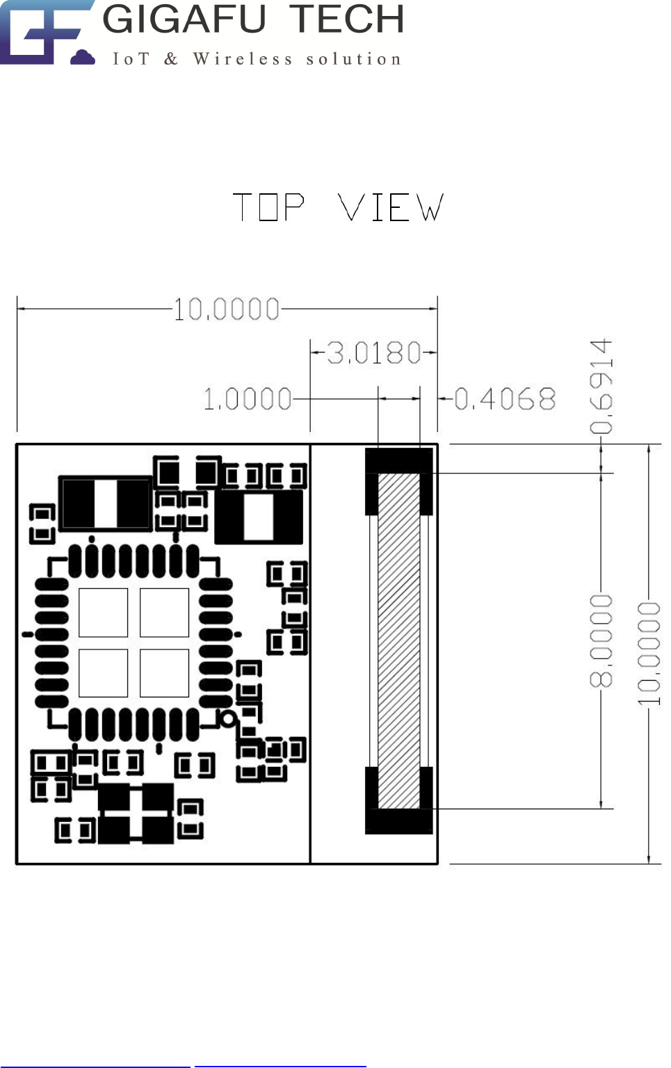
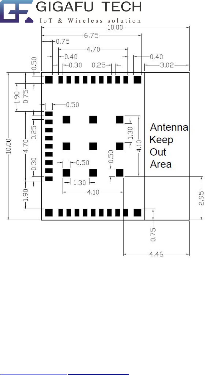
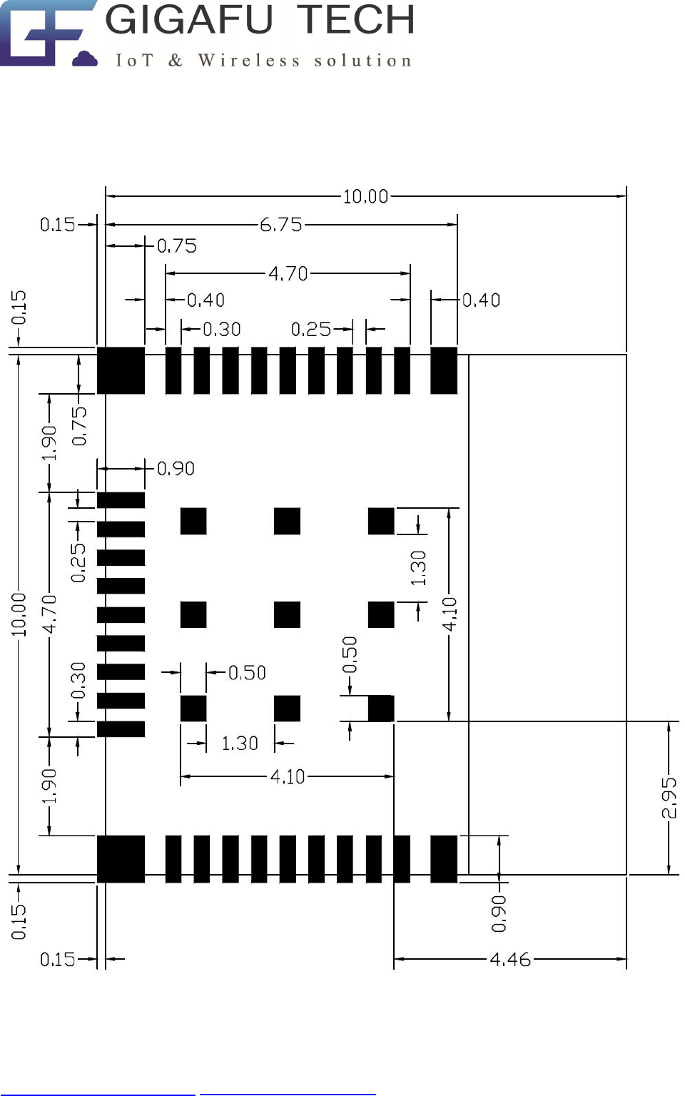
9.1 Outline Dimension (Unit: mm)
Note1 : 3.018mm * 10mm, This is antenna keep out area in the your application.
Gigafu Technology Inc. http://www.gigafu.com.tw/ Proprietary & Confidential Information 16
May-14/2018
Gigafu Technology Inc. http://www.gigafu.com.tw/ Proprietary & Confidential Information 17
May-14/2018
Gigafu Technology Inc. http://www.gigafu.com.tw/ Proprietary & Confidential Information 18
May-14/2018
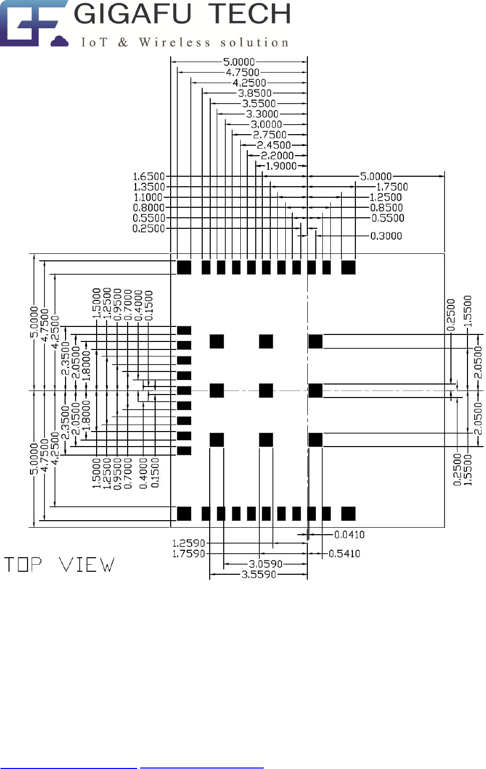
9.2 Recommended Footprint (Unit: mm)
< TOP VIEW >
Gigafu Technology Inc. http://www.gigafu.com.tw/ Proprietary & Confidential Information 19
May-14/2018
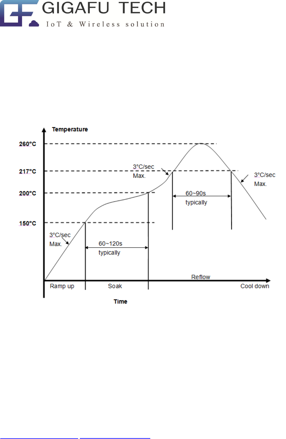
10. Recommended Reflow Profile
1. Referred to IPC/JEDEC standard
2. Peak Temperature : <260°C
3. Cycle of Reflow : 2 times max.
4. Nitrogen reflow is recommended, less than 2000ppm of oxygen concentration.
5. If the shelf time is exceeded, be sure baking step to remove the moisture from the
component.
Gigafu Technology Inc. http://www.gigafu.com.tw/ Proprietary & Confidential Information 20
May-14/2018
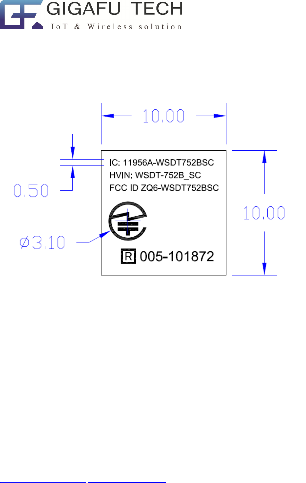
11. Label Drawing
(Unit: mm)

Gigafu Technology Inc. http://www.gigafu.com.tw/ Proprietary & Confidential Information 21
May-14/2018
12. Packing Information
12.1 Packing Dimension
TBD

Gigafu Technology Inc. http://www.gigafu.com.tw/ Proprietary & Confidential Information 22
May-14/2018
13.Statement
13.1 FCC Statement:
This device complies with part 15 of the FCC Rules. Operation is subject to the following two
conditions:
(1) This device may not cause harmful interference, and
(2) This device must accept any interference received, including interference that may
cause undesired operation.
13.2 ISED Statement:
This device complies with Industry Canada license-exempt RSS standard(s). Operation is
subject to the following two conditions: (1) this device may not cause interference, and (2)
this device must accept any interference, including interference that may cause undesired
operation of the device.
Le present appareil est conforme aux CNR d'Industrie Canada applicables aux appareils
radio exempts de licence. L'exploitation est autorisee aux deux conditions suivantes : (1)
l'appareil ne doit pas produire de brouillage, et (2) l'utilisateur de l'appareil doit accepter tout
brouillage radioelectrique subi, meme si le brouillage est susceptible d'en compromettre le
fonctionnement.
In accordance with FCC Part 15C and RSP-100, this module is listed as a Modular
Transmitter device.
Changes or modifications not expressly approved by the manufacturer could void the user’s
authority to operate the equipment.

Gigafu Technology Inc. http://www.gigafu.com.tw/ Proprietary & Confidential Information 23
May-14/2018
The antenna of this transmitter must not be co-located or operating in conjunction with any
other antenna or transmitters within a host device, except in accordance with FCC
multitransmitter product approval procedures.
13.3 FCC Label Instructions
The outside of final products that contains this module device must display a label
referring to the enclosed module. This exterior label can use wording such as the
following: “Contains Transmitter Module FCC ID: ZQ6-WSDT752BSC” or “Contains FCC
ID: ZQ6-WSDT752BSC.” Any similar wording that expresses the same meaning may be
used.
Additionally, there must be the following sentence on the device, unless it is too small to
carry it:
“This device complies with part 15 of the FCC Rules. Operation is subject to the following two
conditions:
(1) This device may not cause harmful interference, and (2) this device must accept any
interference received, including interference that may cause undesired operation.”
If the final product is to be sold in Canada, then this exterior label should use wording
such as the following: “Contains Transmitter Module IC: 11956A-WSDT752BSC”