ASSALOY Identification Technologies H102022RFPCHR PCMCIA Compact Flash Card Reader (RF-ID) User Manual Part 1
ASSA ABLOY Identification Technologies GmbH PCMCIA Compact Flash Card Reader (RF-ID) Users Manual Part 1
Contents
- 1. Users Manual Part 1
- 2. Users Manual Part 2
Users Manual Part 1

Firmware: 0.9v 10/10/2003, wk
ACG Identification Technologies GmbH
Dantestrasse 4-6
65189 Wiesbaden
Germany
Fon +49 (611) 1739.0
Fax +49 (611) 1739.198
www.acg.de rfid@acg-id.net
13,56 MHz Multitag Reader
Module
H102022, H6160

13,56 MHz Multitag Reader Module, Version 0.9v
ACG Identification Technologies AT Page 1
Table of Content
1 Scope ..................................................................................................3
2 Definitions and abbreviations ...........................................................4
2.1 Definitions:......................................................................................................... 4
2.1.1 Anticollision loop......................................................................................... 4
2.1.2 Hex notation................................................................................................ 4
2.1.3 ASCII notation............................................................................................. 4
2.2 Abbreviations..................................................................................................... 4
3 Tag organization.................................................................................5
3.1 State diagram.................................................................................................... 5
3.2 Supported labels ............................................................................................... 6
3.3 ISO 15693 ......................................................................................................... 7
3.3.1 Coding of UID ............................................................................................. 7
3.3.2 Memory organization .................................................................................. 7
3.3.3 My-D Label (SRF55VxxP)........................................................................... 8
3.3.4 EM 4135 ..................................................................................................... 9
3.4 Icode®............................................................................................................... 9
3.4.1 Memory organization .................................................................................. 9
3.4.2 Serial number ............................................................................................. 9
3.4.3 Write access condition.............................................................................. 10
3.4.4 Special function (EAS), AFI ...................................................................... 10
3.4.5 User data .................................................................................................. 10
3.5 TAGIT®........................................................................................................... 10
3.6 SR176 ............................................................................................................. 11
3.6.1 Memory organization ................................................................................ 11
3.6.2 Serial number UID .................................................................................... 11
3.6.3 Lock byte .................................................................................................. 11
3.6.4 Chip ID...................................................................................................... 11
3.7 ISO 14443 ....................................................................................................... 12
3.8 Mifare® Ultralight............................................................................................. 12
3.8.1 Memory organization ................................................................................ 12
3.8.2 Serial number ........................................................................................... 12
3.8.3 Lock bytes................................................................................................. 13
3.8.4 OTP bytes................................................................................................. 13
3.8.5 User data .................................................................................................. 13
4 Hardware...........................................................................................14
4.1 Pin out of OEM Module ................................................................................... 14
4.1.1 Pin out of J1.............................................................................................. 14
4.1.2 Pin out of J2.............................................................................................. 15
4.1.3 Electrical characteristics of PINs............................................................... 15
5 Software............................................................................................16
5.1 ASCII Protocol................................................................................................. 16
5.2 Binary Protocol................................................................................................ 16
5.2.1 STX........................................................................................................... 16
5.2.2 Station ID.................................................................................................. 16
5.2.3 Length....................................................................................................... 16
5.2.4 Data.......................................................................................................... 16
5.2.5 Block Check Character (BCC) .................................................................. 16

13,56 MHz Multitag Reader Module, Version 0.9v
ACG Identification Technologies AT Page 2
5.2.6 ETX........................................................................................................... 17
5.2.7 Remarks ................................................................................................... 17
5.2.8 Examples:................................................................................................. 17
5.3 Instruction Set ................................................................................................. 18
5.3.1 Overview................................................................................................... 18
5.3.2 Error Codes .............................................................................................. 19
5.3.3 EEPROM memory organization................................................................ 19
5.3.4 Reset ........................................................................................................ 24
5.3.5 Get Version............................................................................................... 24
5.3.6 Continuous Read...................................................................................... 25
5.3.7 Select........................................................................................................ 27
5.3.8 Multi Tag Selection / List........................................................................... 28
5.3.9 Read page ................................................................................................ 29
5.3.10 Read reader EEPROM ........................................................................... 30
5.3.11 Write page .............................................................................................. 31
5.3.12 Write EEPROM....................................................................................... 32
5.3.13 Set tag type............................................................................................. 33
5.3.14 Include tag type ...................................................................................... 34
5.3.15 Exclude tag type ..................................................................................... 34
5.3.16 Lock page ............................................................................................... 35
5.3.17 Transfer data telegram............................................................................ 36
5.3.18 Set LED .................................................................................................. 39
5.3.19 Get ID ..................................................................................................... 39
5.3.20 Antenna power on/off.............................................................................. 41
5.3.21 Read/Write User Port.............................................................................. 42
6 Timing ...............................................................................................43
7 Frequently Ask Questions...............................................................46
7.1 Getting started................................................................................................. 46
7.2 How can I adjust the reading performance of different tags? .......................... 46
7.2.1 Remarks ................................................................................................... 46
7.3 Release notes ................................................................................................. 47
7.3.1 Version 0.9x.............................................................................................. 47
7.3.2 Revision History........................................................................................ 47
8 APPENDIX A .....................................................................................48
8.1 P & P module (version 3)................................................................................. 48
8.1.1 Pin out....................................................................................................... 48
8.1.2 Supply voltage 12V................................................................................... 49
8.1.3 RS485/422................................................................................................ 49
9 APPENDIX B:....................................................................................50
9.1 Antenna design ............................................................................................... 50
9.1.1 Layout....................................................................................................... 50
9.1.2 Mechanical data:....................................................................................... 50
9.1.3 Electrical data ........................................................................................... 50
9.1.4 Antenna matching circuit:.......................................................................... 51
10 APPENDIX C ...................................................................................52
10.1 TempSense® KSW Transponder.................................................................. 52
10.1.1 How to start with ..................................................................................... 52
11 References......................................................................................53

13,56 MHz Multitag Reader Module, Version 0.9v
ACG Identification Technologies AT Page 3
1 Scope
The 13,56 MHz Multitag Reader Module is a proximity reading device supporting a
wide range of 13,56 MHz tag. It supports ISO15693, Icode®, Tagit®, Mifare®
Standard, Mifare® Ultralight, SR176 and ISO14443 Type B cards. Using an external
antenna and a serial interface it can be easily connected to a PC. The Plug and Play
version has an integrated antenna and serial interface.
The first part of the documentation described general functions and memory
management of different tags. A listing of the memory map is given in detail if
necessary.
The second part lists the OEM module and describes the pin out.
The next chapter lists all commands and introduce to them. Each command is
explained and an example illustrates the usage. FAQs highlight general issues of the
handling of the 13,56 MHz Multitag Reader Module.
The appendices describes the Plug and Play Module, the custom coil design,
matching circuit and all steps to upgrade the Plug and Play board to +12V supply
voltage.
Additionally the use of the TempeSense® label is high lightened.
WARRANTY
THIS WARRANTY ONLY APPLIES TO THE H6160 DEVICE.
THIS DEVICE COMPLIES WITH PART 15 OF THE FCC RULES. OPERATION IS
SUBJECT TO THE FOLLOWING TWO CONDITIONS: (1) THIS DEVICE MAY NOT
CAUSE HARMFUL INTERFERENCE, AND (2) THIS DEVICE MUST ACCEPT ANY
INTERFERENCE RECEIVED, INCLUDING INTERFERENCE THAT MAY CAUSE
UNDESIRED OPERATION.
CAUTION:
ANY CHANGES OR MODIFICATIONS NOT EXPRESSLY APPROVED BY THE
PARTY RESPONSIBLE FOR COMPLIANCE COULD VOID THE USER’S
AUTHORITY TO OPERATE THE EQUIPMENT.

13,56 MHz Multitag Reader Module, Version 0.9v
ACG Identification Technologies AT Page 4
2 Definitions and abbreviations
2.1 Definitions:
2.1.1 Anticollision loop
Algorithm processed to identify and handle a dialogue between VCD and one or
more VICCs in its antenna field.
2.1.2 Hex notation
A hexadecimal value is noted with a following h. i.e. A1h has the value A1
hexadecimal.
2.1.3 ASCII notation
ASCII characters are listed within apostrophes, i.e. ‘x’ means a single x.
2.2 Abbreviations
AFI Application family identifier
BCC Binary Calculated Checksum
CRC Cyclic redundancy check
DSFID Data storage format identifier
ETX End of transmission frame
LSB Least significant bit
MFR Manufacturer
MSB Most significant bit
RFU Reserved for future use
OTP One time programming
STATID Station ID
STX Start of transmission frame
UID Unique identifier
VCD Vicinity coupling device
VICC Vicinity integrated circuit card
Figure 2-1: Abbreviations
13,56 MHz Multitag Reader Module, Version 0.9v
ACG Identification Technologies AT Page 5
3 Tag organization
3.1 State diagram
Figure 3-1: State Diagram
The state diagram shows the different states of a tag. First the tag must be power up.
Next command initialize a tag using the anticollision or inventory command.
A selection of a tag is necessary to interact with a tag of interest especially if more
than one tag is present at the same time. Only selected tags are capable to response
to higher commands such as read or write page data.
READY state A tag enters the READY state after it receives a
valid inventory or anticollision command. At this
state the tag all serial numbers are known and
the tag is ready to select.
ACTIVE state After a selection the tag is in the ACTIVE state.
Only an activated tag can respond to a read or
write command.
HALT state The HALT command disables a tag for further
communication. The tag is still in the field but
dies not respond to any command. To activate a
tag and to put it back to the Ready state a
WAKE-UP command has to be used.
Power off
Ready
A
CTIVE
HALT
Anticollision Loop,
Inventor
y
WAKE-UP
Application
Select

13,56 MHz Multitag Reader Module, Version 0.9v
ACG Identification Technologies AT Page 6
3.2 Supported labels
Comments
Encryption not supported
Temperature logging
Limited reading performance
Limited reading performance
Limited reading performance
Limited reading performance
Limited reading performance
Limited reading performance
Limited reading performance
Transfer
command
(1)
√
√
√
√
√
√
√
-
-
-
-
-
-
-
-
-
Lock
page
√
√
√
√
-
√
-
√
√
-
√
-
-
-
-
√
Write
page
√
√
√
√
-
√
√
√
√
-
√
-
-
-
-
√
Read
page
√
√
√
√
-
√
√
√
√
-
√
-
-
-
-
√
Serial
number
√
√
√
√
√
√
√
√
√
√
√
√
√
√
√
√
Manufacturer
EM Microelec.
Philips
STM
Infineon
Infineon
TI
KSW
TI
Philips
Philips
Philips
Philips
Philips
Infineon
Infineon
STM
ISO15693
EM 4135
Icode® SLI
LRI512
SRF55VxxP
SRF55VxxS
Tagit® HFI
TempSense
Tagit®
Icode®
ISO14443A
Mifare® Std.
Mifare® Ultralight
MF1IC70
Mifare ProX
SLE55R16
ISO14443B
SLE66CL160S
SR176
Figure 3-2: Supported tags
(1) Only commands within 320µs after the EOF are recognized

13,56 MHz Multitag Reader Module, Version 0.9v
ACG Identification Technologies AT Page 7
3.3 ISO 15693
The reader can communicate with ISO15693 tags. An anticollision is needed if
multiple instances of tags are in the same antenna field. The reader detects each
type of ISO15693 labels and handles them individually
3.3.1 Coding of UID
The UID of a tag is defined in ISO/IEC 15693-3. All tags compliant to ISO15693
support the specified format. The UID is factory programmed and cannot be
changed. The UID is needed for the anticollision sequence to separate several tags
in the same antenna field.
Byte
7 6 5 4 3 2 1 0
E0h MFR
Code Serial number
Figure 3-3: Coding of ISO 15693 UID
The MFR Code is listed in ISO/IEC 7816-6:1996/Amd.1: 2000(E). Following
manufacturer are tested with our reader
MFR-Code Company
02h ST Microelectronics
04h Philips Semiconductors
05h Infineon Technologies AG
07h Texas Instrument
16h EM Microelectronic-Marin SA
Figure 3-4: Manufacturer codes
3.3.2 Memory organization
An ISO15693 tag is separated into two blocks. An administrative block which
contains the UID, AFI, DSFID and the lock page state. The user block is free for
custom use. The chip manufacturer defines the amount of bytes and number of
pages of each tag. As default four bytes are used for several tags.
Byte
Page
address 0 1 2 3
3Fh User data
… …
00h User data
Administrative block
Figure 3-5: Memory organization of ISO 15693
13,56 MHz Multitag Reader Module, Version 0.9v
ACG Identification Technologies AT Page 8
3.3.3 My-D Label (SRF55VxxP)
My-D labels are specific labels of Infineon. These labels show a different memory
organization. Two different modes of tags are supported: plain and secure mode. At
the moment only plain mode tags are supported in full functionality. Only serial
numbers are supported in secure mode.
Two different cards with 320 bytes or 1k bytes EEPROM memory are available. The
EEPROM memory is divided into pages.
Each tag is split into two parts: The administrative blocks (00h, 01h, 02h) and the
user area. Administrative pages are read only and cannot be changed. User data is
free for use. Additionally user data pages can be locked. This procedure is
irreversible.
The EEPROM of SRF55V10P is organized in 128 pages addressed 00h to 7Fh. The
EEPROM of SRF55V02P consists of 32 pages addressed 00h to 1Fh.
Page
Address 0 1 2 3 4 5 6 7
7Fh User data
… …
3Fh User data
… …
03h User data
02h
01h
00h Serial number (UID)
SRF55V02P
SRF55V10P
Figure 3-6: SRF55VxxP memory organization
3.3.3.1 UID
The UID of SRF55Vxx labels starts with 60h or E0h.
3.3.3.2 Security Bit
Bit 45 of the UID defines the secure mode of the SRF55Vxx. If set the tag supports
security algorithm and is not accessible with the reader device
Bit 45 Description
1 Tag supports crypto security mechanism
0 Chip supports plain mode only
Figure 3-7: Security bit
13,56 MHz Multitag Reader Module, Version 0.9v
ACG Identification Technologies AT Page 9
3.3.4 EM 4135
The EM4135 is an ISO15693 compliant label of EM Microelectronic-Marin SA. It has
eight bytes per page as the same as the My-D label. It only supports 35 pages. The
administrative area holds the information of the access condition and the UID.
Page
Address 0 1 2 3 4 5 6 7
24h User data
… …
00h User data
Administrative area
Figure 3-8: Memory organization of EM 4135
3.4 Icode®
Icode® labels stores data is stored in a non-volatile EEPROM. Its capacity is 512 bits
organized in 16 blocks consisting 4 bytes each (1 block = 32 bits). First 3 blocks
contain administrative data.
3.4.1 Memory organization
Byte
Page
address 0 1 2 3
0Fh User data
… …
05h User data
04h Family code identifier / User data
03h Special function (EAS) / User data
02h Write access condition
01h Serial number
00h Serial number
Figure 3-9: Icode® memory organization
3.4.2 Serial number
The serial number of a label is defined at the manufacturer process. It is stored on
page 00h and page 01h. LSB is stored first.

13,56 MHz Multitag Reader Module, Version 0.9v
ACG Identification Technologies AT Page 10
3.4.3 Write access condition
Page 02h contains the write access condition for each page. Each page can be set to
read only (bits are set to 0). This procedure is irreversible. Locking page 2 no further
changed of the access condition can be done. Always two bits must be change at the
same time. This register is implemented as OTP.
Byte 0 Byte 1 Byte 2 Byte 3
MSB LSB MSB LSB MSB LSB MSB LSB
1 1 1 1 0 0 0 0 1 1 1 1 11111111111111 1 1 1 1 11
3 2 1 0 7 6 5 4 B A 9 8 F E D C
Special
function
Write
access
Serial
numbe
r
Serial
numbe
r
User
data
…
…
…
…
…
…
…
…
…
…
User
data
Figure 3-10: Write access condition bytes
3.4.4 Special function (EAS), AFI
Special Functions (EAS) and Family Code/Application Identifier are additional
features. For more information refer to the Icode® manual.
3.4.5 User data
All other blocks are free for use and can be changed according the state of the write
access conditions.
3.5 TAGIT®
TAGIT® labels are organized in a wide range of different page size and number of
pages. Automatically the reader detects the correct memory organization.
Switching on the Extended ID mode (see chapter instruction set) the reader appends
two bytes to the UID containing the page size and the number of pages of a label.
13,56 MHz Multitag Reader Module, Version 0.9v
ACG Identification Technologies AT Page 11
3.6 SR176
The SR176 label contains only 64 bytes of data organized in two bytes per page.
3.6.1 Memory organization
Page
address Byte 1 Byte 0
0Fh Lock byte RFU Chip ID
0Eh User data
… …
04h User data
03h Serial number
02h Serial number
01h Serial number
00h Serial number
Figure 3-11: SR176 memory organization
3.6.2 Serial number UID
The UID is stored at the first 4 pages. Page 00h contains the LSB of the UID.
Page 03h Page 02h Page 01h Page 00h
Byte 1h Byte 0 Byte 1 Byte 0 Byte 1 Byte 0 Byte 1 Byte 0
Figure 3-12: SR176 Serial number
3.6.3 Lock byte
The lock byte defines the write access condition of a pair of pages. Each bit can only
be set once. This procedure is irreversible. This byte is implemented as OTP.
Bit 7 Bit 6 Bit 5 Bit 4 Bit 3 Bit 2 Bit 1 Bit 0
Page 0Eh
Page 0Fh
Page 0Ch
Page 0Dh
Page 0Ah
Page 0Bh
Page 08h
Page 09h
Page 06h
Page 07h
Page 04h
Page 05h
Page 02h
Page 03h
Page 00h
Page 01h
Figure 3-13: Lock byte
3.6.4 Chip ID
The Chip ID is defined in the low nibble of page 0Fh. It is manufacturer set and is
used internally to select and separate single tags.
13,56 MHz Multitag Reader Module, Version 0.9v
ACG Identification Technologies AT Page 12
3.7 ISO 14443
The reader can only handle single tags according ISO 14443 type A or B. The reader
only identifies single tags and returns its serial number.
All other command such as read, write, select are not supported.
The Mifare® transponder family consists of various 13.56 MHZ transponders
according to ISO14443. For more details refer to ISO14443 part 1-4.
3.8 Mifare® Ultralight
Mifare® Ultralight tags have no crypto algorithm included. They are designed for a
small data volume.
3.8.1 Memory organization
Byte
Page
address 3 2 1 0
0Fh User data
…
04h User data
03h OTP
02h Lock bytes reserved
01h Serial number
00h Serial number
Figure 3-14: Memory organization of Mifare® Ultralight
3.8.2 Serial number
The UID consists of 7 bytes. The first part of the UID is stored on page 00h the
second on page 01h. The storage format on page 00h fulfills ISO14443 Type A. The
UID is factory programmed and cannot be changed.

13,56 MHz Multitag Reader Module, Version 0.9v
ACG Identification Technologies AT Page 13
3.8.3 Lock bytes
On page 2 the lock bytes are stored. Each bit specifies a page or block. Once a bit is
set it cannot be changed anymore. This process is irreversible. If a block lock bit is
set all pages within this block are read only regardless the single lock states. This
register is implemented as OTP
Byte 1 Byte 0
MSB LSB MSB LSB
7 6 5 4 3 2 1 0 7 6 5 4 3 2 1 0
Page F
Page E
Page D
Page C
Page B
Page A
Page 9
Page 8
Page 7
Page 6
Page 5
Page 4
OTP
Block A-F
Block 4-9
OTP
Figure 3-15: Lock bytes of Mifare® Ultralight
3.8.4 OTP bytes
Page 3 is implemented as OTP register. All bits are factory programmed to 0. Once a
bit is set it cannot be changed furthermore. It can be used as a 32 bit one-time
counter.
3.8.5 User data
User data is free for use. It can be changed according the write access condition.
13,56 MHz Multitag Reader Module, Version 0.9v
ACG Identification Technologies AT Page 14
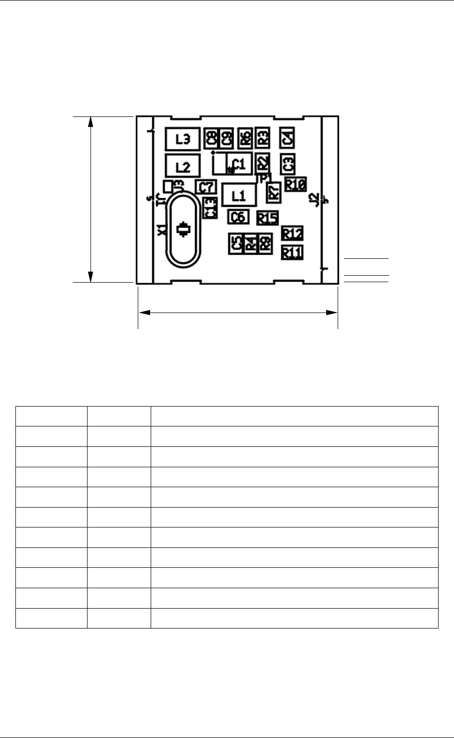
4 Hardware
4.1 Pin out of OEM Module
Figure 4-1: Pin out of the reader device
4.1.1 Pin out of J1
PIN PIN Nr Description
ARX 1 Antenna RX
ATX1 2 Antenna TX1
VDD 3 +5 V DC
GND 4 Ground
RFU 5 Reserved for future use
TGND 6 Antenna Ground
RFU 7 Reserved for future use
RFU 8 Reserved for future use
RFU 9 Reserved for future use
RFU 10 Reserved for future use
Figure 4-2: Pin out of jumper 1
30,5
25,5
2,54
1,27
J1
J2

13,56 MHz Multitag Reader Module, Version 0.9v
ACG Identification Technologies AT Page 15
4.1.2 Pin out of J2
PIN PIN Nr Description
VDD 20 +5 V DC
GND 19 Ground
LEDg 18 LED green (reading LED)
LEDr 17 LED red
EN 16 Enable reader, open or logic high
RFU 15 Reserved for future use
USER 14 User Port
DIR 13 Direction of RS 485
TX 12 TX to PC
RX 11 RX from PC
Figure 4-3: Pin out of jumper 2
4.1.3 Electrical characteristics of PINs
PIN PIN Nr Voltage Current
(max) Description
RX
TX 11
12 USART2 - To RS232, RS485 device
driver
USER 14 TTL3 25 mA User sets logic state
EN 16 ST4 25 mA Low will disable the
reader device
LEDr 17 GND 25 mA Logic Low, used for LED
LEDg 18 LED 25 mA
With 330 Ω (internal)
ARX
ATX1
TGND
1
2
6
(depends
on antenna
tuning)
200 mAPP Antenna input
Antenna output
Antenna output (GND)
RFU 5,7,8,9,
10,15 - - Not connected
GND 4,19 GND - Supply Ground
VDD 3,20 +5 V DC 150 mA Supply Voltage
DIR 13 TTL 25 mA RS485 direction
Figure 4-4: Electrical characteristics of pins
2 Universal Synchronous Asynchronous Receiver Transmitter
3 TTL buffer output / input
4 Schmitt trigger buffer output

13,56 MHz Multitag Reader Module, Version 0.9v
ACG Identification Technologies AT Page 16
5 Software
As a default data is transmitted at 9600,n,8,1. Two protocol modes are supported.
The protocol mode is configured in the reader EEPROM. As factory default, the
ASCII protocol is used.
5.1 ASCII Protocol
This protocol was designed for easy handling. The commands can be issued using a
terminal program. Data is transmitted as ASCII hexadecimal that can be displayed on
any terminal program (e.g. HyperTerminal).
Command Data
Various length Various length
Figure 5-1: ASCII protocol frame
5.2 Binary Protocol
This protocol was designed for industrial applications with synchronization and frame
checking. Also an addressing byte for party lines (master slave, multi drop) is
included.
The protocol usually requires a device driver. Data is transmitted binary.
STX Station ID Length Data BCC ETX
1 byte 1 byte 1 byte Various length 1 byte 1 byte
Figure 5-2: Binary protocol frame
5.2.1 STX
Start of transmission (02h)
5.2.2 Station ID
Unique ID of the station
00h: reserved for the bus master. Readers send response to this device ID
FFh: Broadcast message. All devices will execute the command.
5.2.3 Length
Length of the data block
5.2.4 Data
This part contains the command and data. The command values are the same as in
ASCII protocol mode (‘x’, ‘s’, …). Data is transmitted binary.
The length of the command block depends on the instruction.
5.2.5 Block Check Character (BCC)
The BCC is used to detect transmission errors. The BCC is calculated XORing each
byte of the transmission frame excluding the STX/BCC and ETX character.
)/(...)/()()( 0N
DataCommandxorxorDataCommandxorLengthxorStatIDBCC =

13,56 MHz Multitag Reader Module, Version 0.9v
ACG Identification Technologies AT Page 17
5.2.6 ETX
End of transmission. (03h)
5.2.7 Remarks
If the reader device receives an invalid instruction frame (i.e. BCC wrong) or the
requested station ID does not match the internal ID of the reader, the command is not
executed. The reader waits for the next valid frame.
Use the binary timeout (see protocol configuration register) to detect incomplete
binary frames.
5.2.8 Examples:
02h 64h 01h 78h 1Dh 03h
STX Station ID Length ‘x’ BCC ETX
This instruction frame will reset the reader module with the station ID 64h.

13,56 MHz Multitag Reader Module, Version 0.9v
ACG Identification Technologies AT Page 18
5.3 Instruction Set
Following table describes all commands of the reader device. Each command returns
an answer to the host. Exceptions are mentioned explicitly. The green LED is
acknowledging a successfully executed command. The red LED indicates an error.
5.3.1 Overview
Command Description
‘x’ Reset
‘v’ Get version
‘c’ Continuous read
‘s’ Select
‘m’ MultiTag select / tag list
‘r’ Read page
‘rp’ Read EEPROM register
‘w’ Write page
‘wp’ Write EEPROM register
‘oX’ Set tag type
‘o+X’ Include tag type
‘o-X’ Exclude tag type
‘k’ Lock page
‘t’ Transfer data telegram
‘dr’ / ’dg’ / ‘dn’ Set LED
‘g’ Get ID
‘poff’ / ’pon’ Antenna power off/on
‘pr’ / ’pw’ Read / write user port
Figure 5-3: Command overview

13,56 MHz Multitag Reader Module, Version 0.9v
ACG Identification Technologies AT Page 19
5.3.2 Error Codes
Following figure shows an overview of all error messages of the reader device.
Error Code Description
‘?’ Unknown command
‘F’ General failure
‘I’ Invalid data format, this error occurs only in ASCII mode. The
reader assumes a hexadecimal value but receives bad data
‘N’ No tag in the field
‘U’ Read data does not match written data, block might be write
protected or write process fails.
‘X’ Page is already locked. Lock command fails
Figure 5-4: Error codes
5.3.3 EEPROM memory organization
Following figure lists the EEPROM register of the reader device.
Page Description
00h…04h Unique device ID; read only
05h…09h administrative data, RFU
0Ah Station ID
0Bh Protocol configuration
0Ch Baud rate
0Dh Binary watchdog timer
0Eh Operation mode
0Fh Timeout value
10h RFU
11h Start page
12h Number of pages
13h…1Fh RFU
20h…FFh User data
Figure 5-5: EEPROM memory

13,56 MHz Multitag Reader Module, Version 0.9v
ACG Identification Technologies AT Page 20
5.3.3.1 Unique device ID (00h-04h)
The unique device ID identifies a reader module. It is factory programmed and cannot
be changed.
5.3.3.2 Station ID (0Ah)
The station ID is used in binary mode to address a device in party line set up. The
station ID has the rage of 01h to FEh and can be freely set. The value 00h is
reserved for the bus master. All readers send a response to this device.
The broadcast message (FFh) forces all readers to response to the command.
Default value is 01h.
5.3.3.3 Protocol configuration (0Bh)
The PCON register specifies general behavior of the reader device.
Default value is 01h.
Protocol configuration register
Bit 7 Bit 6 Bit 5 Bit 4 Bit 3 Bit 2 Bit 1 Bit 0
Extend-
ed ID Page
read Single
shot LED Lock
mode BWDT Protocol Auto
start
Figure 5-6: Protocol configuration register
5.3.3.3.1 Auto start (default 1)
If set the reader device will start up in continuous read mode automatically. Auto start
has only effect in ASCII protocol mode.
5.3.3.3.2 Protocol (default 0)
If set the reader uses binary protocol mode. As default ASCII protocol is used. See
section binary protocol for further information on the binary protocol format.
5.3.3.3.3 Binary timeout (default 0)
If set the reader sets up a binary timeout internally. This bit should be enabled in
binary protocol mode to ensure correct framing.
5.3.3.3.4 Lock mode (default 0)
If set the reader locks itself to the first recognized tag type automatically. Other tag
types are not recognized. Only a reset or a change operation mode command
cancels the lock state.
5.3.3.3.5 LED (default 0)
If set the reader suppresses any LED activity. The user manages the state of the
LEDs.

13,56 MHz Multitag Reader Module, Version 0.9v
ACG Identification Technologies AT Page 21
5.3.3.3.6 Single shot (default 0)
If set the reader displays the serial number of a tag only once within a specified
timeout. The time out is defined at EEPROM register 0Fh. 00h indicated no delay.
The delay time can be adjusted stepwise in 100 msec steps.
5.3.3.3.7 Page read (default 0)
If set the reader sends the content of a page specified at EEPROM register 11h
instead of the serial number. Additionally the reader device reads following pages
defined at EEPROM register 12h.
5.3.3.3.8 Extend ID (default 0)
If set Tagit® and ISO14443 Type B cards returns additional information.
Tag type Number of
Bytes Description
Tagit® 2 page size, number of pages
ISO14443B 7 application data, Protocol Identifier
Figure 5-7: Extended ID
5.3.3.4 Baud rate (0Ch)
The baud rate register defines the communication speed of the reader device.
Default value is 00h.
Baud rate register
Bit 7 Bit 6 Bit 5 Bit 4 Bit 3 Bit 2 Bit 1 Bit 0
RFU RFU RFU RFU RFU RFU BS1 BS0
Figure 5-8: Baud rate register
This register defines the baud rate of the device.
BS1 BS0 Baud rate
0 0 9600 baud (default)
0 1 19200 baud
1 0 38400 baud
1 1 57600 baud
Figure 5-9: Baud rate settings

13,56 MHz Multitag Reader Module, Version 0.9v
ACG Identification Technologies AT Page 22
Following figure describes the communication settings
Description
8 data bits
No parity bit
1 stop bit
No flow control
Figure 5-10: Communication settings
5.3.3.5 Binary watchdog timer (0Dh)
The binary watchdog timer defines the maximum delay time between two byte in
binary protocol mode sent from the host to the reader. In binary protocol mode the
binary watchdog timer should be enabled in order to detect incomplete or corrupted
frames.
The value FFh is revered and should not be used.
The value 00h sets the timeout to a minimum.
Default value is FEh.
5.3.3.6 Operation mode (0Eh)
The operation mode register defines which tag types the reader supports. This
register enables fast tag recognition because only defined tag types are requested.
Operation mode register
Bit 7
(MSB) Bit 6 Bit 5 Bit 4 Bit 3 Bit 2 Bit 1 Bit 0
(LSB)
RFU
RFU
SR176
ISO14443B
ISO1443A
Icode®
Tagit®
ISO15693
Figure 5-11: Operation mode register
5.3.3.7 Timeout value (0Fh)
The timeout value defines the delay time between two responses of the reader. It has
only effect in continuous read mode. To enable the timeout the single shot flag has to
be set. See above protocol configuration register. One timeout slice is 100msec.
Exact timing depends on the used protocol.
Value 00h indicates no delay time.
Default value is 0Ah (1 sec).

13,56 MHz Multitag Reader Module, Version 0.9v
ACG Identification Technologies AT Page 23
5.3.3.8 Start page (10h)
The EEPROM register defines the start page address in page read mode. To enable
this function the page read flag has to be set. See above protocol configuration
register.
The reader will send the content of this page instead of the serial number. This mode
is only supported for ISO15693, Icode® and Tagit® tags. The reader does not check
the integrity of the page address. If an error occurs or a not valid page is read nothing
is returned.
Default value is 00h.
5.3.3.9 Number of pages (12h)
The number of pages describes how many following pages are read. The start
address is specified at EEPROM register 10h. The reader returns all pages and
sends in the end a <CR> + <LF>. In binary protocol mode each page is send
separately. No terminator is sent in the end.
Value 00h is reserved and should not be used.
Default value is 01h (one page is read).
5.3.3.10 User data (20h-FFh)
User data is free for use.

13,56 MHz Multitag Reader Module, Version 0.9v
ACG Identification Technologies AT Page 24
5.3.4 Reset
This command executes a power on (software) reset. New configuration settings will
be loaded.
5.3.4.1 Command
Command Data
‘x’ none
5.3.4.2 Answer
Answer Description
none ASCII Mode: “ISO 1.0” + CR + LF
Binary Mode: none
This command will reset the reader module as well as all tags in the antenna field.
The reader starts according the startup settings.
5.3.4.3 Reset Timing
The power up timing depends on environmental conditions such as voltage ramp up.
For handheld devices the timing may depend on the charging state of the battery.
5.3.5 Get Version
This command returns the current version of the reader module.
5.3.5.1 Command
Command Data
‘v’ none
5.3.5.2 Answer
Answer Description
none ASCII Mode: “ISO 1.0” + CR + LF
Binary Mode: 02 00 07 49 53 4F 20 31 2E 30 31 03
5.3.5.3 Example
Command Description
v ISO 1.0
Version of the reader module

13,56 MHz Multitag Reader Module, Version 0.9v
ACG Identification Technologies AT Page 25
5.3.6 Continuous Read
The reader device reads and displays the serial numbers continuously while one or
more tags remain in the field. This command stops if any character is sent to the
reader module. The reader module returns the character ‘S’ (53h).
Only different tag types are detected at the same time. Use the multitag list command
(see chapter 5.3.8) if more than one ISO15693 tag are present.
The reader supports different tag types. Though a single continuous read instruction
needs a specific time. To increase the reading performance switch to a single tag
mode. Results depend on the startup conditions. See chapter read EEPROM register
for more details of startup configurations.
5.3.6.1 Command
Command Data
‘c’ none
5.3.6.2 Answer
Answer Description
data Leading character (1 byte) + serial number (n bytes)
Number of bytes depends on tag type.
This command is not supported in binary protocol mode.
5.3.6.3 Leading character
The leading character specifies a single tag type. It can be used to determine the
present tag type and control tag specific commands. Card types have different UID
length, e.g. ISO15693 cards use an 8 byte UID whereas standard ISO14443 Type A
cards 4.
Following table describes all leading characters of supported tag types.
Tag type UID length Description
‘V’ 8 bytes ISO 15693
‘T’ 4 bytes Tagit®
‘I’ 8 bytes Icode®
‘M’ Var. size Mifare® Ultralight, ISO 14443 Type A
‘S’ 8 bytes SR176
‘Z’ 4 bytes ISO1443 Type B
Figure 5-12: Leading character of continuous read mode

13,56 MHz Multitag Reader Module, Version 0.9v
ACG Identification Technologies AT Page 26
5.3.6.4 Continuous read mode at start up (default enabled)
Continuous read mode at startup could be activated using the utility program.
5.3.6.5 Lock mode (default disabled)
If set the reader locks to the first recognized tag type. This speeds up the
communication to a tag in continuous read mode. The reader only uses this tag type
anymore.
5.3.6.6 Extended ID (default disabled)
If set Tagit® and ISO14443 Type B cards returns additional information.
Tag type Number of
Bytes Description
Tagit® 2 page size, number of pages
ISO14443B 7 Application data, Protocol Identifier
Figure 5-13: Extended ID
5.3.6.7 SingleShot function (default disabled)
If enabled the reader replies the serial number only once. Then the reader waits until
a timeout is reached. One time slice is around 100 ms. The timeout value has the
range of one byte and is stored in EEPROM register 0Fh.
5.3.6.8 PageRead function (default disabled)
If enabled the reader sends a page content instead of the serial number back to the
host. The reader starts at the page specified in the EEPROM register 11h and reads
as many as following pages defined at EEPROM register 12h. A single command is
terminated with an <CR> + <LF>.
In binary protocol mode each page is transmitted separately. At the end no <CR> +
<LF> is transmitted.
5.3.6.9 LED function (default disabled)
Using the LED active flag the reader suppresses an activity of the LED. The user can
set the LED state using the commands of switching on/off LED.
5.3.6.10 Simple access control applications
Serial numbers are not encrypted and always sent plain to the reader. This results in
a low-level security application.

13,56 MHz Multitag Reader Module, Version 0.9v
ACG Identification Technologies AT Page 27
5.3.7 Select
This command selects a single card in the antenna field. It can only be used in single
tag mode. In case of success the command returns the UID of the selected card.
5.3.7.1 Command
Command Data
‘s’ none
5.3.7.2 Answer
Answer Description
data Leading character (1 byte) + serial number
‘N’ Error: No Tag in the field
5.3.7.3 Select a single tag
No previous continuous read is required.
5.3.7.4 Extended ID (default)
If set Tagit® and ISO14443 Type B cards return additional information. See above for
more information of the Extended ID.
5.3.7.5 Multiple tags
This command is designed for fast access to a single tag in the field. If multiple cards
are used in the field the ‘m’ instruction for the select procedure has to be used.
5.3.7.6 Example
s E000112233445566
Select the card of type ISO15693 with the UID
E000112233445566

13,56 MHz Multitag Reader Module, Version 0.9v
ACG Identification Technologies AT Page 28
5.3.8 Multi Tag Selection / List
This command detects several ISO15693 tags at the same time. It replaces the fast
select command in multiple tag surroundings. The Multi Tag list command lists all
tags with its serial numbers. Using the Multi Tag Select command to address a single
or a group of tag together. Each tag has to be selected separately
5.3.8.1 Command
Command Data
‘m’ Serial number (8 bytes)
5.3.8.2 Answer
Answer Description
data ‘V’ + serial number (8 bytes)
‘N’ Error: No Tag in the field
5.3.8.3 Multi tag list
Sending a <CR> (0Dh) as first parameter the reader returns a list of all present tags
in the field. In the end the amount of detect tags are returned. A Multi Tag list
command resets all tags in the antenna field.
5.3.8.4 Reading distance
Each card needs a specific amount of power. The reader always provides the same
power. Therefore the reading distance will decrease if more tags are present.
5.3.8.5 Multi tag select
Using the eight-byte serial number as parameter the according tag will be selected.
High-level interactions can be performed addressing only this card. All other tags are
still present but not used.
5.3.8.6 Maximum number of tags
The maximum number of tags in the antenna field is limited to the physical
characteristics of the antenna. Internally the software can handle up to 40 tags
(theoretical maximum).
5.3.8.7 Example
Command Description
m<CR> VE000123456789012 –> first card
VE000112233445566 –> second card
02 –> number of detect tags
mE000123456789012 E000123456789012
Select card with its serial number

13,56 MHz Multitag Reader Module, Version 0.9v
ACG Identification Technologies AT Page 29
5.3.9 Read page
This command reads a data block on a card. Size of returned data depends on the
used tag. A valid page address depends on the present tag. E.g. an Icode® tag
supports only 16 pages, an ISO15693 SRF55V10P 128 pages.
5.3.9.1 Command
Command Data
‘r’ page address (1 byte)
5.3.9.2 Answer
Answer Description
data page data (depends on tag type)
‘F’ Error: read failure
‘N’ Error: No tag in field
5.3.9.3 Page data
Page data depends on the used tag. Following table describes the default page
sizes. Internally the reader handles the correct data frame size.
Tag type Page size Description
ISO15693 4
8 As default
SRF50VxxP, EM 4135
Tagit® Var. size Depends on tag organization
Icode® 4
SR176 2
Mifare®
Ultralight 4
ISO14443A - Not supported
ISO14443B - Not supported
Figure 5-14: page data
5.3.9.4 No tag in field ‘N’
The tag does not respond. There is either no tag present or not addressed.
5.3.9.5 Read failure ‘F’
This error is displayed if the reader receives bad data. Additionally this error is
generated if a page is read which is not physically located on the card.

13,56 MHz Multitag Reader Module, Version 0.9v
ACG Identification Technologies AT Page 30
5.3.9.6 Examples
r05 00112233
reads page 05. page data is 00112233
5.3.10 Read reader EEPROM
Reads the internal reader EEPROM. It contains all startup parameters and the device
ID. Changes of the startup settings will only be taken into effect after a reset of the
device.
5.3.10.1 Command
Command Data
‘rp’ EEPROM address (1 byte)
5.3.10.2 Answer
Answer Description
data EEPROM data (1 bytes)
5.3.10.3 Example
Command Description
rp0B 01
Reads protocol configuration register.

13,56 MHz Multitag Reader Module, Version 0.9v
ACG Identification Technologies AT Page 31
5.3.11 Write page
This command writes data to a page. A read after write is done automatically to
ensure correct writing.
5.3.11.1 Command
Command Data
‘w’ page address (1 byte) + data (n bytes)
5.3.11.2 Answer
Answer Description
data ‘w’ + page data (depends on tag type)
‘N’ Error: No tag in field
‘F’ Error: Write failure
‘U’ Error: read after write incorrect
5.3.11.3 Page data
Page data depends on the used tag. Following table describes the default page
sizes. Internally the reader handles the correct data frame size.
Tag type Page size Description
ISO15693 4
8 As default
SRF50VxxP, EM 4135
Tagit® n Depends on tag organization
Icode® 4
SR176 2
Mifare®
Ultralight 4
ISO14443A - Not supported
ISO14443B - Not supported
Figure 5-15: page data
5.3.11.4 No tag error ‘N’
This error is returned if no tag is present.
5.3.11.5 Write failure ‘F’
This error is displayed if bad transmission conditions are given. If the page address
exceeds the physical number of pages of a tag this error is thrown too.
13,56 MHz Multitag Reader Module, Version 0.9v
ACG Identification Technologies AT Page 32
5.3.11.6 Read after write error ‘U’
After each write access to a TAG a read is done automatically. This error is thrown if
read data does not match the written data. E.g. the page is read only.
5.3.11.7 Example
Command Description
w0511223344 w11223344
writes data 11223344 on page 05.
5.3.12 Write EEPROM
Writes to the internal reader EEPROM. It contains all startup parameters and the
device ID. Changes of the startup settings will only be taken into effect after a reset of
the device.
5.3.12.1 Command
Command Data
‘wp’ page address (1 byte) + data (1 byte)
5.3.12.2 Answer
Answer Description
data EEPROM data (1 bytes)
5.3.12.3 Example
Command Description
wp0A01 01
Set EEPROM address 0A (Station ID) to 01h

13,56 MHz Multitag Reader Module, Version 0.9v
ACG Identification Technologies AT Page 33
5.3.13 Set tag type
This command switches the reader to a specific tag type. The continuous read
function will speed up because only this tag type is recognized. These changes are
not stored into the EEPROM. After a reset the reader starts as defined in the startup
configuration.
5.3.13.1 Command
Command Data
‘o’ Leading character (1 byte)
5.3.13.2 Answer
Answer Description
none String of tag type
5.3.13.3 Leading character
Tag type String Description
‘a’ “ALL” All tag types
‘i “ICODE“ Icode®
‘m’ “ISO14443A” Mifare® Ultralight, ISO 14443 Type A
‘s’ “SR176” SR176
‘t’ “TAGIT” Tagit®
‘v’ “ISO15693” ISO 15693
‘z’ “ISO14443B” ISO1443 Type B
Figure 5-16: List of leading characters
5.3.13.4 Example
Command Description
ov ISO15693
Set the reader device to ISO15693 tags

13,56 MHz Multitag Reader Module, Version 0.9v
ACG Identification Technologies AT Page 34
5.3.14 Include tag type
This command includes a specific tag type to the reader device.
5.3.14.1 Command
Command Data
‘o+’ Leading character (1 byte)
5.3.14.2 Answer
Answer Description
none String of tag type
5.3.14.3 Leading character
See chapter 5.3.13.3.
5.3.14.4 Example
Command Description
o+t +TAGIT
Include Tagit® protocol to the reader device
5.3.15 Exclude tag type
This command excludes a specific tag type from the reader device.
5.3.15.1 Command
Command Data
‘o-’ Leading character (1 byte)
5.3.15.2 Answer
Answer Description
none String of tag type
5.3.15.3 Leading character
See 5.3.13.3.
13,56 MHz Multitag Reader Module, Version 0.9v
ACG Identification Technologies AT Page 35
5.3.15.4 Example
Command Description
o-i -ICODE
Exclude Icode® protocol from the reader
device
5.3.16 Lock page
This command locks a page permanently. It only supports ISO15693 and Tagit®
tags. Icode® and Mifare® Ultralight tags can be locked using the write command.
See tag organization for more details.
5.3.16.1 Command
Command Data
‘k’ Page address (1 byte)
5.3.16.2 Answer
Answer Description
data ‘k’ + page address
‘F’ Error: Lock failure
‘X’ Error: Page already locked
5.3.16.3 Example
Command Description
k05 K05
Lock page 05.
13,56 MHz Multitag Reader Module, Version 0.9v
ACG Identification Technologies AT Page 36
5.3.17 Transfer data telegram
This command sends a custom data block to a card. First the proper tag type has to
be specified using the set tag type command. The reader device only supports
ISO15693. The command shows a specific command frame for each tag type.
The maximum frame size is limited to 200 bytes each.
5.3.17.1 ISO15693
The reader set the according flag of the protocol automatically. Only FM and high
data rate can be used.
5.3.17.2 Command
Command Data
‘t’ Downlink length (1 byte) + Uplink length (1 byte) + data (n
bytes)
5.3.17.3 Answer
Answer Description
data Response of card
‘F’ Error: General failure
5.3.17.4 Downlink length
The downlink length includes only the data. The CRC is computed automatically and
shall not be included.
5.3.17.5 Uplink length
The uplink length is need due to no length information is included in the protocol. The
user has to know the exact response length of the command. The CRC shall not be
included in the length.
5.3.17.6 Data
Data consists of following frame.
Flags Command code UID Data
(1 byte) (1 byte) (8 bytes) (n bytes)
Figure 5-17: ISO15693 data frame

13,56 MHz Multitag Reader Module, Version 0.9v
ACG Identification Technologies AT Page 37
5.3.17.6.1 Flags
Flags have to be correct in order to succeed. Following figure describes the flag byte.
RFU bits are set automatically and cannot be changed. The inventory flag has to be
set executing the inventory command.
Bit Flag name Value Description
0 RFU 1 Reserved for future use
1 RFU 1 Reserved for future use
0 Flags bit 5 to 8 see Figure 5-19 2 Inventory
1 Flags bit 5 to 8 see Figure 5-20
3 RFU 0 Reserved for future use
Figure 5-18: ISO15693 request flags bit 0 to 3
Bit Flag name Value Description
0 Command is executed according the
address flag.
4 Select
1 Only selected tags execute the command.
The address flag shall be set to 0
0 UID is not included in the command. 5 Address
1 UID is included. Only the addressed tag
executes the command. The select flag
shall be set to 0.
6 Option x Defined in the command code description.
Default is 0.
7 RFU 0 Reserved for future use
Figure 5-19: ISO15693 request flags bit 4 to 7
Bit Flag name Value Description
0 AFI field is not present 4 AFI
1 AFI field is present
0 16 slots 5 Slots
1 1 slot
6 Option x Defined in the command code description.
Default is 0.
7 RFU 0 Reserved for future use
Figure 5-20: ISO15693 request flags bit 4 to 7, inventory flag is set

13,56 MHz Multitag Reader Module, Version 0.9v
ACG Identification Technologies AT Page 38
5.3.17.6.2 Command code
Refer to ISO15693-3 or the tag manufacturer documentation for more details.
5.3.17.6.3 UID
The UID is optional. If address flag is set it is mandatory. Only the addressed VICC
executes the command. All other tags remain quit.
5.3.17.6.4 Data
Depends on command code.
5.3.17.7 Answer
The length of the answer is specified in the uplink length byte. Following figure shows
a complete response data frame.
Flags Data CRC
(1 byte) (n byte) (2 bytes)
Figure 5-21: ISO15693 response format
If the less bytes are send from the card than specified in the length byte following
bytes are even displayed:
Byte 1 Byte 2 - up to length bytes
80h 00h
Figure 5-22: ISO15693 response trailer
5.3.17.7.1 Response flags
Bit Flag name Value Description
0 No error 0 Error
1 Error is thrown
1,2,3,
4,5,6,
7
RFU 0 Reserved for future use
Figure 5-23: ISO15693 response flags
5.3.17.7.2 Error
If the error flag is set the VICC has generated an error. Next byte contains the error
code. Refer to the card manufacturer documentation for specific details of the error.
5.3.17.8 Example
Command Description
T030A270100 000066554433221100E0
Inventory response of card
E000112233445566
13,56 MHz Multitag Reader Module, Version 0.9v
ACG Identification Technologies AT Page 39
5.3.18 Set LED
This command controls the LED. If the LED flag is set the automatic LED is
deactivated. The user can set the state of the LED manually.
5.3.18.1 Command
Command Data
‘d’ LED state (1 byte)
5.3.18.2 Answer
Answer Description
none String of LED state
5.3.18.3 LED
Command Answer Description
‘dg’ DG Switch on LED green, LED red off
‘dr’ DR Switch on LED red, LED green off
‘dn’ DN Switch off both LEDs
Figure 5-24: LED response
5.3.18.4 Examples
Command Description
dr DR
Switch on LED red
5.3.19 Get ID
This command returns the station ID of the reader device. The answer is time slotted
to be able to detect all devices in party line mode.
5.3.19.1 Command
Command Data
‘g’ none
5.3.19.2 Answer
Answer Description
data Station ID of the reader device (1 byte)
13,56 MHz Multitag Reader Module, Version 0.9v
ACG Identification Technologies AT Page 40
5.3.19.2.1 ASCII mode
The station ID has only effect in binary mode.
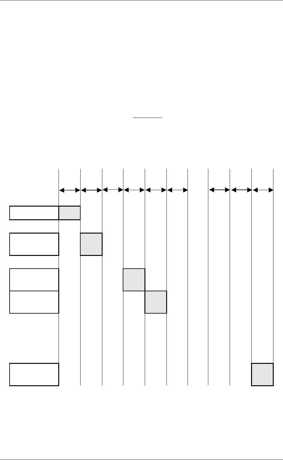
5.3.19.3 Time slotted answer
In party line mode more than one reader can be used simultaneously. The time
slotted answer allows a separation of all connected devices. The station ID is used to
determine the correct time slot.
The reader supports up to 254 unique time slots. Following formula allows calculating
the needed time of one time slot. Only one baud rate on the same party line is
supported.
6*
10
][
0
B
audrate
sT =
Figure 5-25: Time slot formula
Following figure shows a timing diagram of time slotted answers.
timeslot 0 1 2 3 4 5 252 253 254
T0 T1 T2 T3 T4 T5 T253 T254 T255
HOST ‘g’ →
reader (01) ←
01
reader (03) ←
03
reader (04) ←
04
reader (254) ←
254
Figure 5-26: Timing diagram of time slotted answers

13,56 MHz Multitag Reader Module, Version 0.9v
ACG Identification Technologies AT Page 41
5.3.20 Antenna power on/off
This command controls the antenna power.
5.3.20.1 Command
Command Data
‘pon’ Switch on reader
‘poff’ Reader enters the stand by mode
5.3.20.2 Answer
Answer Description
‘P’ Positive acknowledge
5.3.20.3 Power off
The reader enters the stand by mode. Power consumption is decreases. All tags in
the antenna field are powered off and reset. The stand by mode is only entered
manually.
To switch off the whole unit pin 16 (Enable) has to set to logic low.
5.3.20.4 Power on
The reader leaves the stand by mode and is ready for the next command. Sending a
tag command (i.e. select, continuous read) the reader is powered up.
5.3.20.5 Example
Command Description
poff P
Reader enters stand by mode

13,56 MHz Multitag Reader Module, Version 0.9v
ACG Identification Technologies AT Page 42
5.3.21 Read/Write User Port
This command will set or read the state of the USER port (pin 14) of the OEM reader
device. The port can be set either as output or as input.
5.3.21.1 Command
Command Data
‘pr’ none
‘pw’ State of user port (1 Byte)
5.3.21.2 Answer
Answer Description
data State of user port (1 Byte)
5.3.21.3 Read port
The port read command returns the actually state of the USER port.
Port state Description
00 USER port is low
01 USER port is high
Figure 5-27: Read USER port return values
5.3.21.4 Write port
Port state Description
00 Sets USER port to low
01 Sets USER port to high
Figure 5-28: Write User port settings
5.3.21.5 Remarks
If user port is used as an output a 1kΩ resistor has to be integrated into the wire.
Otherwise the reader device may cause damage.
5.3.21.6 Example
Command Description
Pr 00
user port is logic low.
pw01 01
Sets USER port state to high

13,56 MHz Multitag Reader Module, Version 0.9v
ACG Identification Technologies AT Page 43
6 Timing
The timing is measured between request and response of the reader. Additionally to
the process timing the protocol timing must be included. It depends on protocol mode
as well as on the baud rate.
TimeFail TimeTyp TimeMax Command
[ms] [ms] [ms]
Reset 5
Power up - 80,0 85,0
Software (x) - 2,98 3,06
Get version (v) - 0,206 -
Continuous read (c) 6
All - 13,6 164,0
ISO 15693 - 13,6 14,1
Tagit - 20,4 21,0
Icode - 31,0 32,0
SR176 - 26,4 54,0
ISO 14443 Type A - 18,0 19,0
Ultralight - 26,0 27,0
ISO 14443 Type B - 14,8 15,5
Page read (start up option)
All - 22,4 105,0
ISO 15693 - 22,4 23,6
Tagit - 37,6 38,0
Icode - 37,2 38,0
Select (s)
All 392,0 20,5 392,0
ISO 15693 50,8 20,5 21,0
Tagit 81,6 20,4 21,0
Icode 116,0 31,0 32,0
SR176 54,8 26,4 54,0
ISO 14443 Type A 43,8 18,0 19,0
Ultralight 43,8 26,0 27,0
5 Reset will cause an error if reader IC Initialization fails
6 Continuous read will only return successful readings

13,56 MHz Multitag Reader Module, Version 0.9v
ACG Identification Technologies AT Page 44
ISO 14443 Type B 44,2 14,8 15,5
Multitag list (m)
1 card 156,0 85,6 87,0
2 cards 156,0 85,6 87,0
Multitag select (m) 9,2 6,6 7,0
Read page (r)
ISO 15693 25,6 5,28 25,6
Tagit 67,6 17,0 67,6
Icode 34,8 7,0 34,8
SR176 7,6 2,4 7,6
ISO 14443 Type A 18,0 - -
Ultralight 11,6 4,8 11,6
ISO 14443 Type B 0,16 - -
Read EEPROM (rp) - 200 -
Write page (w)
ISO 15693 41,8 19,1 22
Tagit 79,2 45,2 79,2
Icode 52,0 24,0 52,0
SR176 10,4 8,8 10,4
ISO 14443 Type A 24,0 - -
Ultralight 24,0 10,4 24,0
ISO 14443 Type B 0,232 - -
Write EEPROM (wp) - 4,7 -
Set tag type (oX) 7 - 0,154 1,85
Include tag type (o+X) - 1,0 1,36
Exclude tag type (o-X) - 1,0 1,36
Lock page (k)
ISO 15693 272 27,2 30,8
Tagit
Transfer data telegram - Var -
Set LED (dr, dg, dn) - 0,16 -
Get Station ID (g) - 0,16 -
Antenna power on (poff) - 0,24 -
7 depends on tag type

13,56 MHz Multitag Reader Module, Version 0.9v
ACG Identification Technologies AT Page 45
Antenna power off (pon) - 0,24 -
Port read (pr) - 0,20 -
Port write (pw) - 0,16 -
Unknown command 0,24 - -

13,56 MHz Multitag Reader Module, Version 0.9v
ACG Identification Technologies AT Page 46
7 Frequently Ask Questions
7.1 Getting started
To test and interface the ACG 13,56 MHz Multitag OEM Reader Module, no
sophisticated µP development system is needed. All you need is a PC, a connection
cable and a power supply for the reader. If you are using Microsoft Windows
(98/NT/2000…), take following steps:
1. Make sure, that your reader is RS232-interface type
1. Start HyperTerminal
2. Create a new connection (FILE/NEW CONNECTION)
3. Enter name of connection as you like (i.e. ‘ISO 1.0’)
4. Select connect COM2 (COM1) direct connection
5. Connection setup 9600,8,n,1,no handshake
6. Connect the reader to COM2 (COM1) of the PC and apply appropriate the
supply voltage. The reader sends a string to the PC (e.g. “ISO 1.0”). This
string denotes the firmware provided by your reader module
7. Put a tag to your reader. Serial numbers should be displayed properly
8. Enter commands via keyboard. They are transmitted to the reader and the
reader replies with its response.
If using an operating system different from Microsoft Windows you may use any other
terminal program which is capable of receiving/transmitting via the serial port of your
PC.
7.2 How can I adjust the reading performance of different
tags?
Due to different tags of different tag manufacturers the antenna tuning has to be
adapted. The Plug and Play reader module is factory tuned for ISO 15693 tags. To
switch to Mifare tags the tuning capacitor (see APPENDIX A) has to be adjusted
correctly.
Following steps have to be done:
1. Connect the reader to the PC
2. Set the reader to the specific tag type
3. Start continuous reading mode (‘c’)
4. Place a tag within the antenna field.
5. Tune the capacitor until the LED is flickering.
6. Increase the distance between the tag and the reader
7. Repeat steps 5 and 6 until no better performance can be reached.
Now the reader is optimal tuned of a specific tag type.
7.2.1 Remarks
If more than one tag has to be read all steps mentioned above have to be performed
for each tag type. The reading distance of one tag in multi tag recognition mode
might be less than in an optimal tuned antenna field.

13,56 MHz Multitag Reader Module, Version 0.9v
ACG Identification Technologies AT Page 47
7.3 Release notes
7.3.1 Version 0.9x
7.3.1.1 New features added to version 0.9x:
o Anticollision ISO15693
o Single shot of UID including delay time
o Page read as continuous read default
o Set of tag type is selectable
o Tagit® and ISO14443B supports extend ID
o Tagit® lock page
o Set LED manually
o SR176 new edition
o EM4135
7.3.1.2 Changes made to version 0.9x
o Continuous read sends a ‘S’ after quitting
o Leading character of ‘ISO1444B’ has changed to ‘Z’
o ‘MifareB’ tag type has changed to ‘ISO14443B’
o ‘Mifare’ tag type has changed to ‘ISO14443A’
7.3.1.3 Bug fixes
o Transfer data command supports up to 200 bytes
o Icode® is fully supported
o SR176 new is fully supported
o Full support of ISO15693 lock page
7.3.2 Revision History
Date Revision
9/19/2003 Version 0.9v rev 1.0
9/23/2003 0.9v rev 1.1
10/9/2003 0.9v rev 1.2
13,56 MHz Multitag Reader Module, Version 0.9v
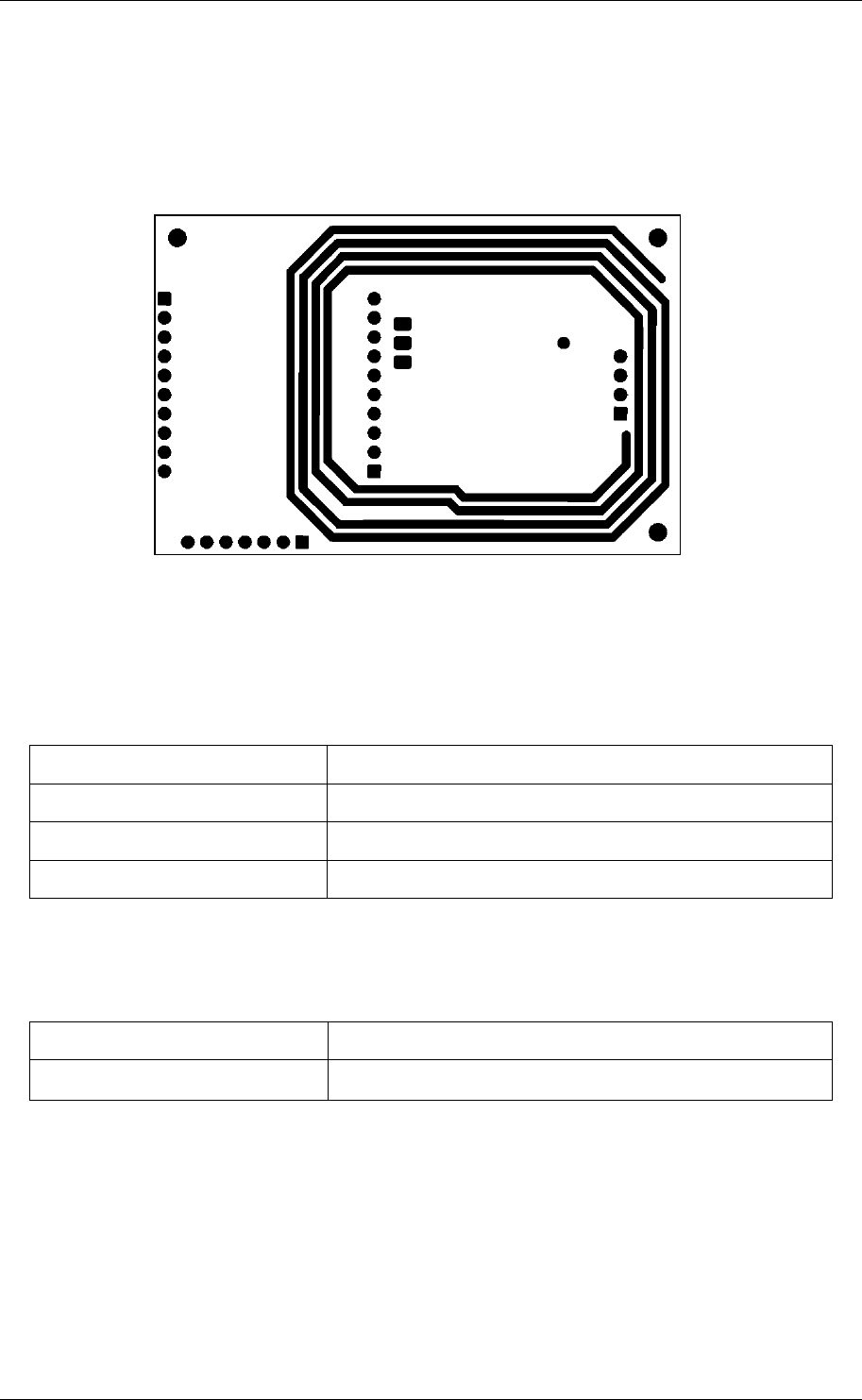
ACG Identification Technologies AT Page 48
70
,
0
8 APPENDIX A
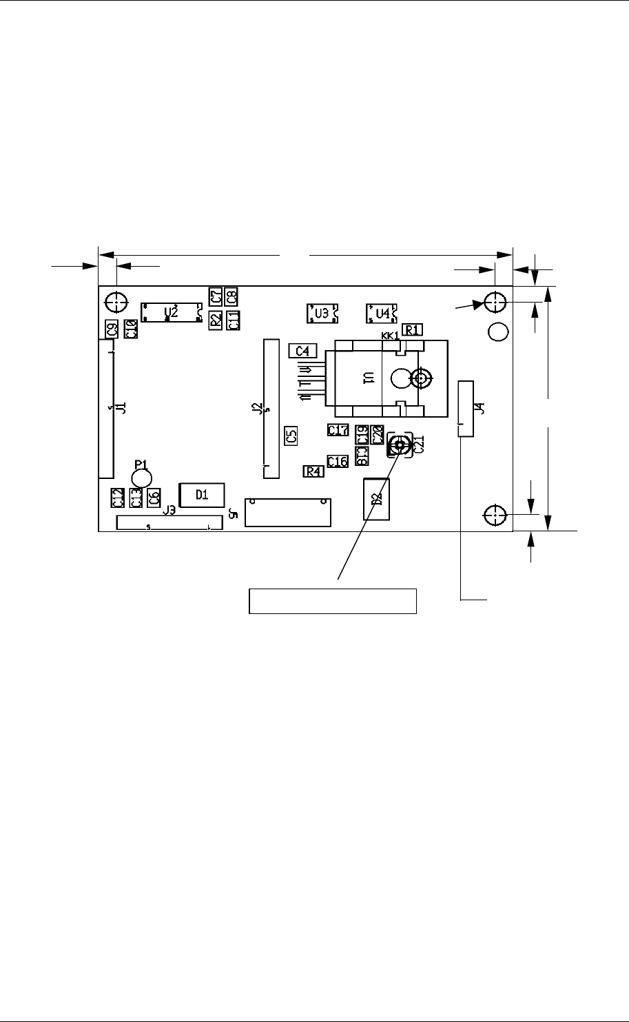
8.1 P & P module (version 3)
8.1.1 Pin out
All distances are listed in mm!
Figure 8-1: Plug & Play Reader Module
Tuning Capacitor
45,5
3 3
3
3
TX B (RS422 OUT)
RX B (RS422 IN)
TX A (RS422 OUT or RS232 OUT)
RX A (RS422 IN or RS232 IN)
GND
+ 5
V
reserved (+ 12V)
Supply LED +
Supply LED –
Reading LED –
Reading LED +
∅2,6

13,56 MHz Multitag Reader Module, Version 0.9v
ACG Identification Technologies AT Page 49
8.1.2 Supply voltage 12V
Following components have to be added:
Component Description
U1 Voltage Regulator 7805
D1 TMM BAT42
C4 330 nF, 50V, Shape 1206
C5 100 nF, 50V, Shape 0805
Figure 8-2: 12 V components
8.1.3 RS485/422
Using the RS485 bus following changes are necessary.
Remove following items:
Component Description
U2 Sipex SP202EEN
Figure 8-3: RS232 device driver
Add following items:
Component Description
U3 Sipex SP485REN
U4 Sipex SP485REN
Figure 8-4: RS485 device driver
8.1.3.1 RS422
RS422 is a four-wire communication. The reader module does not support full duplex
at the same time.
8.1.3.2 RS485
Connect following pins of J3:
Pin Description
4, 5 RXA, TXA, used as line A
6, 7 RXB, TXB, used as line B
Figure 8-5: Pin connection of RS485
13,56 MHz Multitag Reader Module, Version 0.9v
ACG Identification Technologies AT Page 50
9 APPENDIX B:
9.1 Antenna design
9.1.1 Layout
Figure 9-1: Antenna layout
9.1.2 Mechanical data:
Dimension 51x42 mm
Wire width 1,27 mm; 35 um Cu thickness
Distance between 2 turns 1,75 mm
Number of turns 4
Figure 9-2: Coil design - mechanical data
9.1.3 Electrical data
Inductivity 1,2 µH
Resistance 0,33 Ω
Figure 9-3: Coil design – electrical data
13,56 MHz Multitag Reader Module, Version 0.9v
ACG Identification Technologies AT Page 51
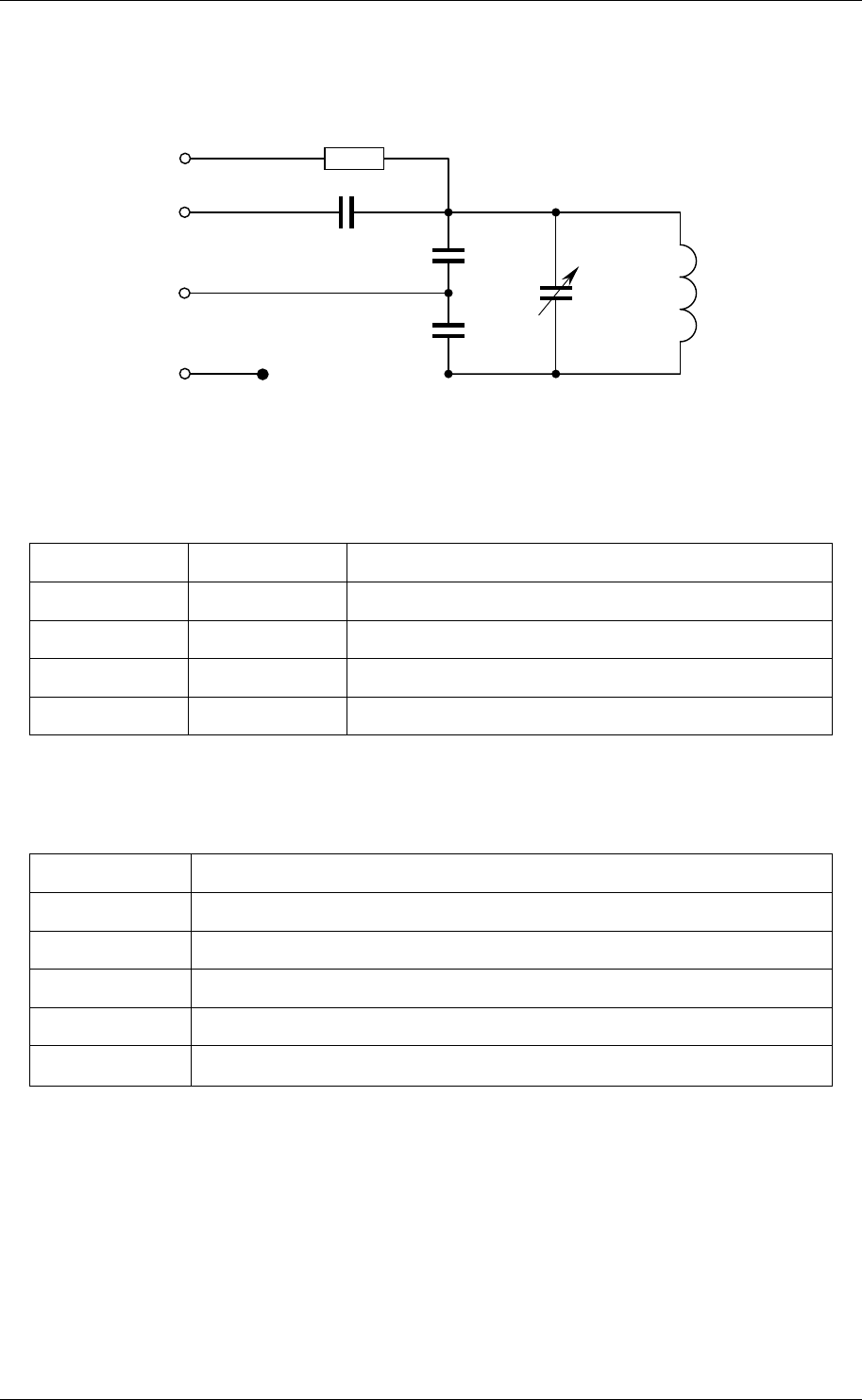
9.1.4 Antenna matching circuit:
Figure 9-4: Antenna matching circuit
9.1.4.1 Connecting scheme
Pin Nr Pin Description
1 ARX Antenna RX
2 ATX1 Antenna TX
5 RFU Not connected
6 TGND Antenna ground
Figure 9-5: Antenna connecting scheme
9.1.4.2 Component values:
Component Description
C1 100 pF
C3 68 pF
C4 0R0 (jumper)
C5 8-40 pF
R 8,2 kΩ
Figure 9-6: Antenna components
C3
C4
R
C1
C5 L
A
nt
Pin 1
Pin 2
Pin 6
Pin 5

13,56 MHz Multitag Reader Module, Version 0.9v
ACG Identification Technologies AT Page 52
10 APPENDIX C
10.1 TempSense® KSW Transponder
The TempSense® KSW transponder is an ISO15693 compliant tag. The reader ahs
to be set up for this tag type.
10.1.1 How to start with
oConnect the module to the power supply and the PC.
oStart the ISO Reader Utility program.
oInquire Reader first in order to get a correct connection to the module
oSwitch to the KSW label.
Alternatively you can use any terminal program (i.e. HyperTerminal).
For more details of the KSW transponder please contact KSW Microtec AG.
http://www.ksw-microtec.de

13,56 MHz Multitag Reader Module, Version 0.9v
ACG Identification Technologies AT Page 53
11 References
ISO/IEC 15693, Part 1-4, Contact less integrated circuit(s) cards – vicinity cards
ISO/IEC 14443, Part 1-4,
TempSense KSW Tags, http://www.ksw-microtec.de