AirM2M Communication Technology AIR208 GSM/GPRS Module User Manual
Shanghai AirM2M Communication Technology Co., Ltd GSM/GPRS Module
UserManual.wiki
>
AirM2M Communication Technology
>
AIR208 User Manual
User Manual
Navigation menu
Upload a User Manual
Namespaces
Wiki Guide
HTML
PDF
Info
Views
User Manual
Discussion / Help
Navigation
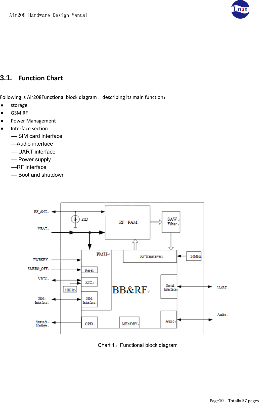
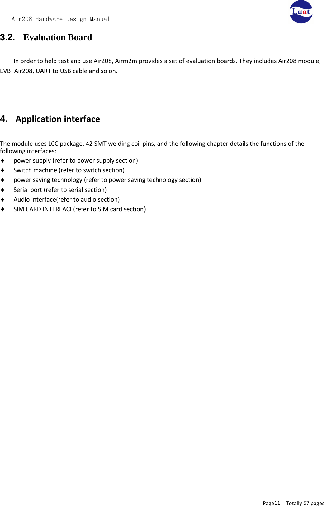
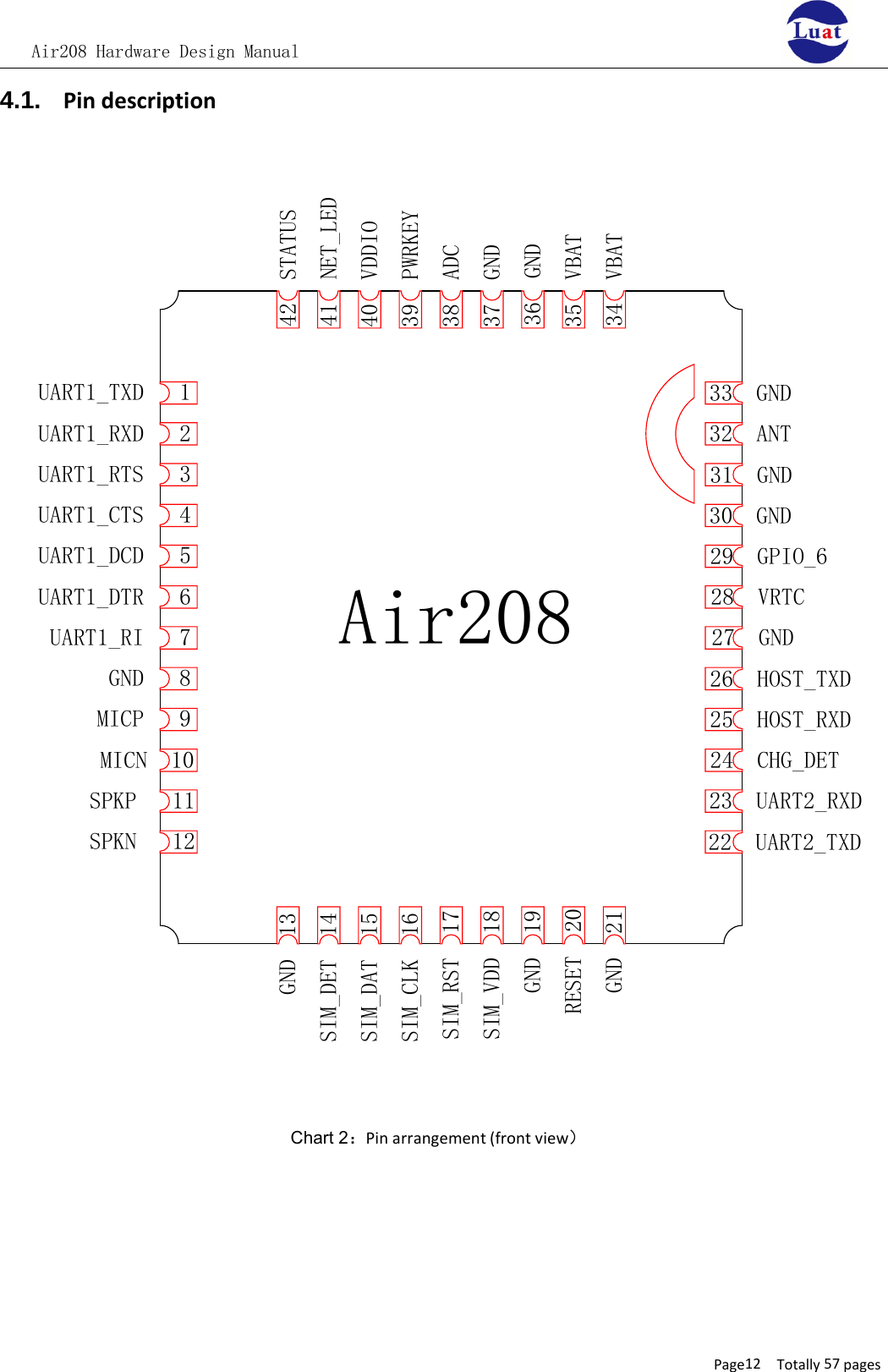
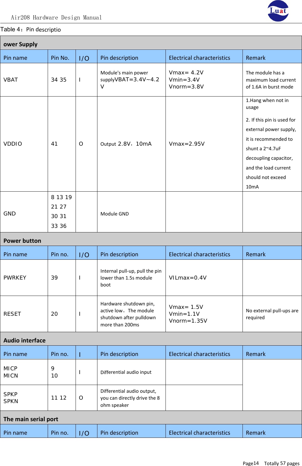
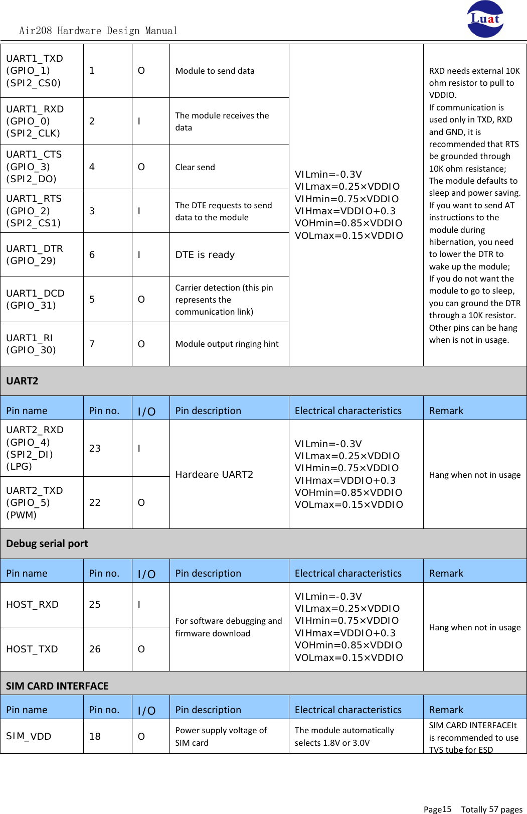
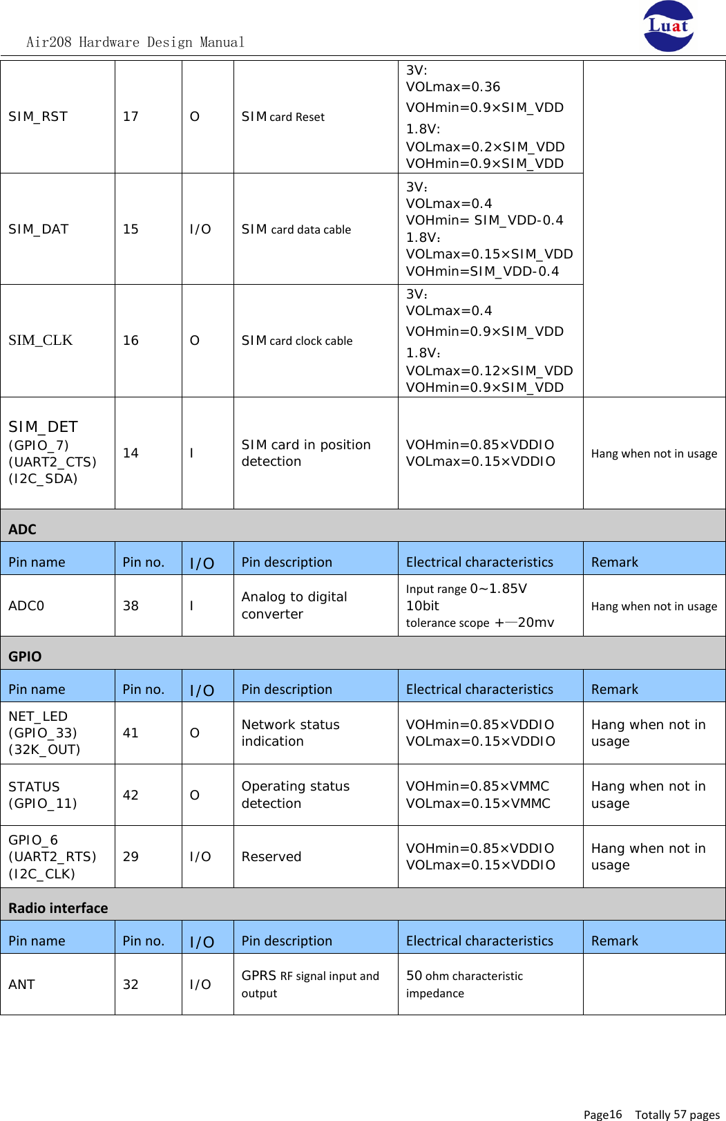
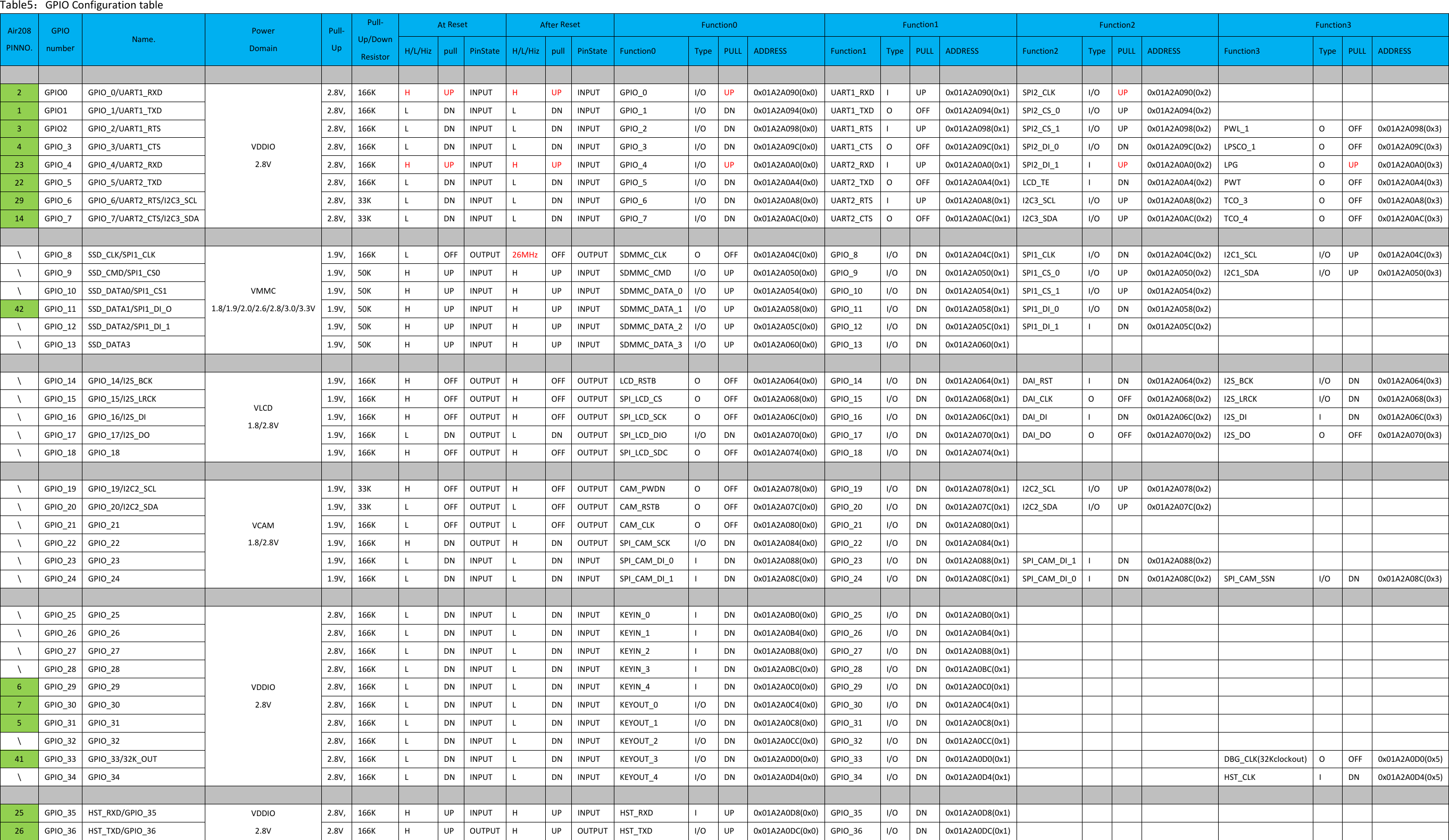
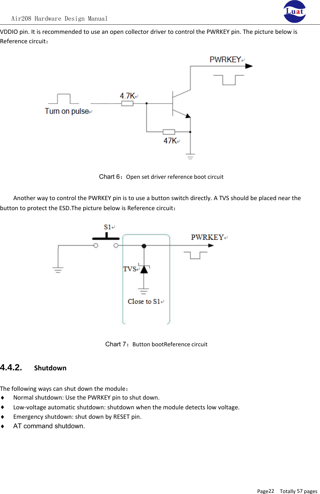
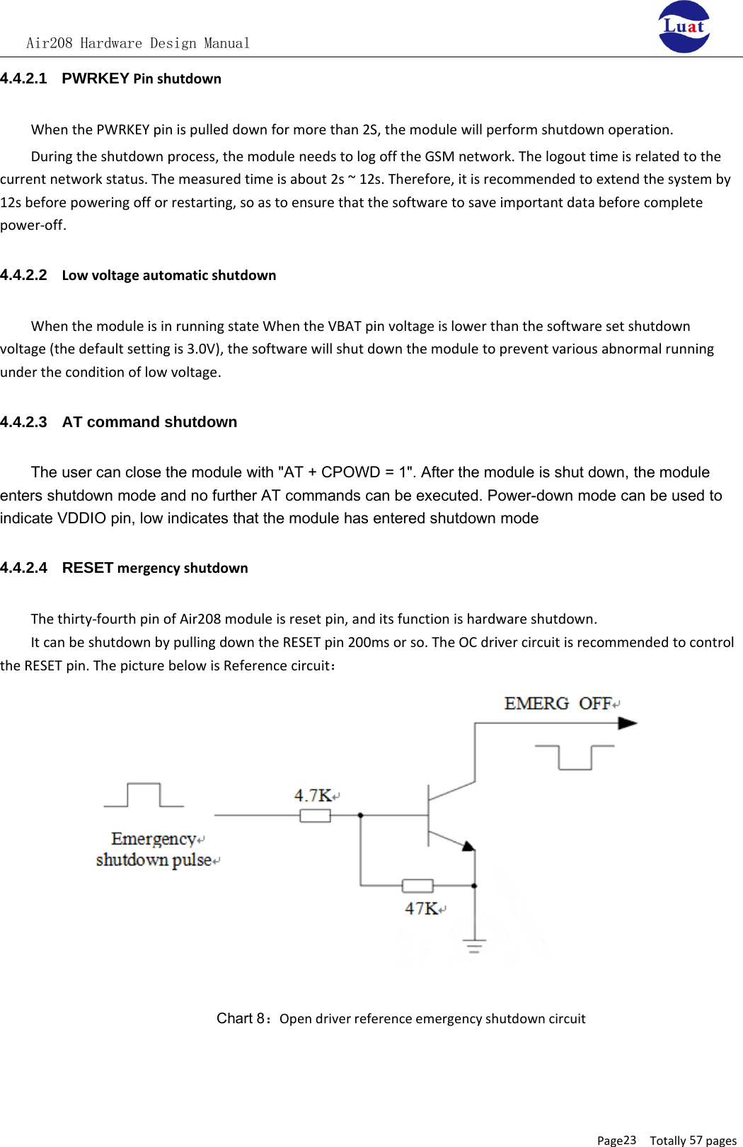
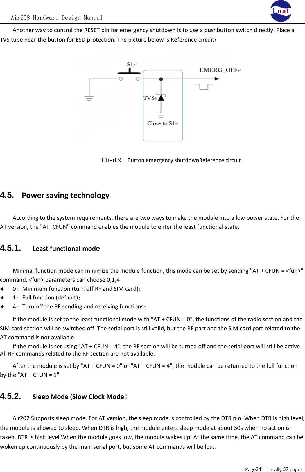
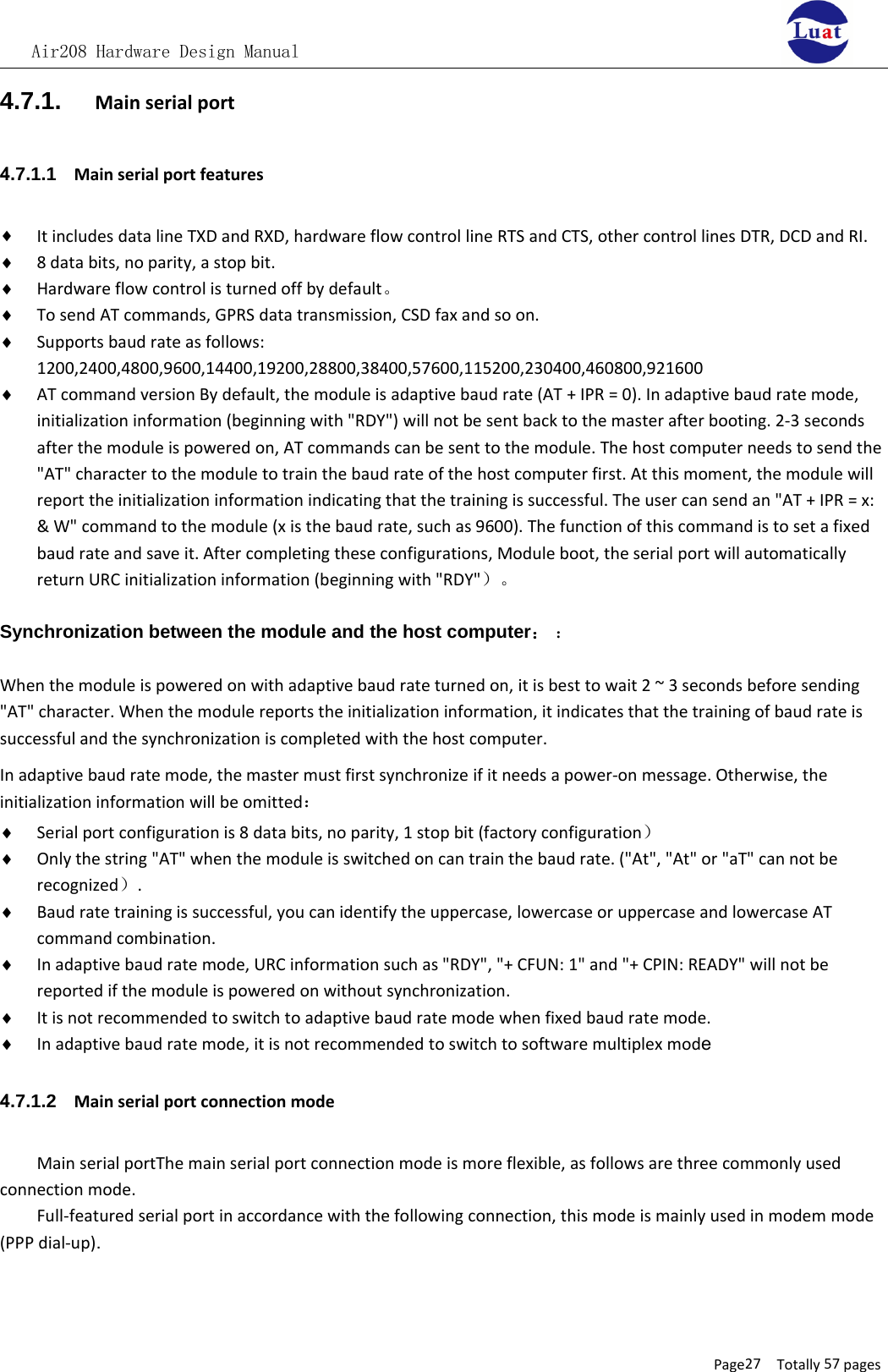
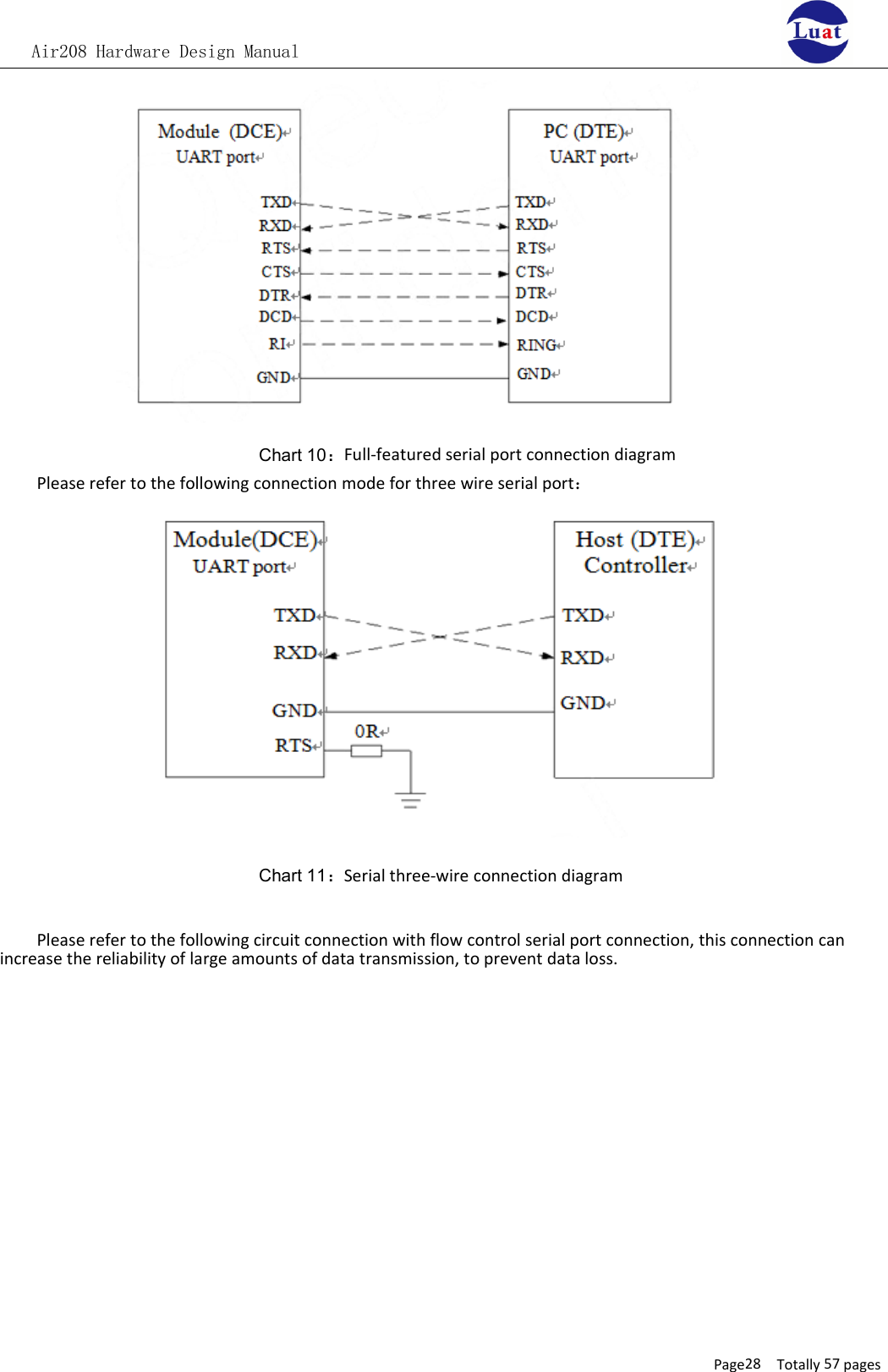
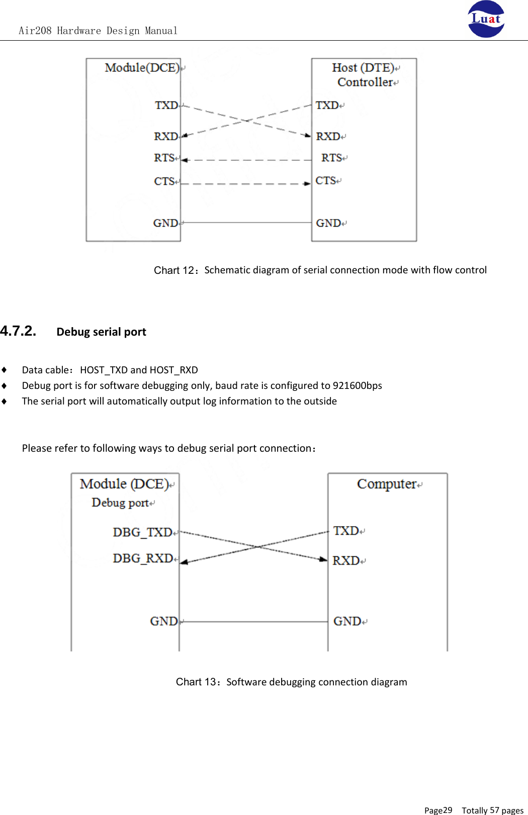
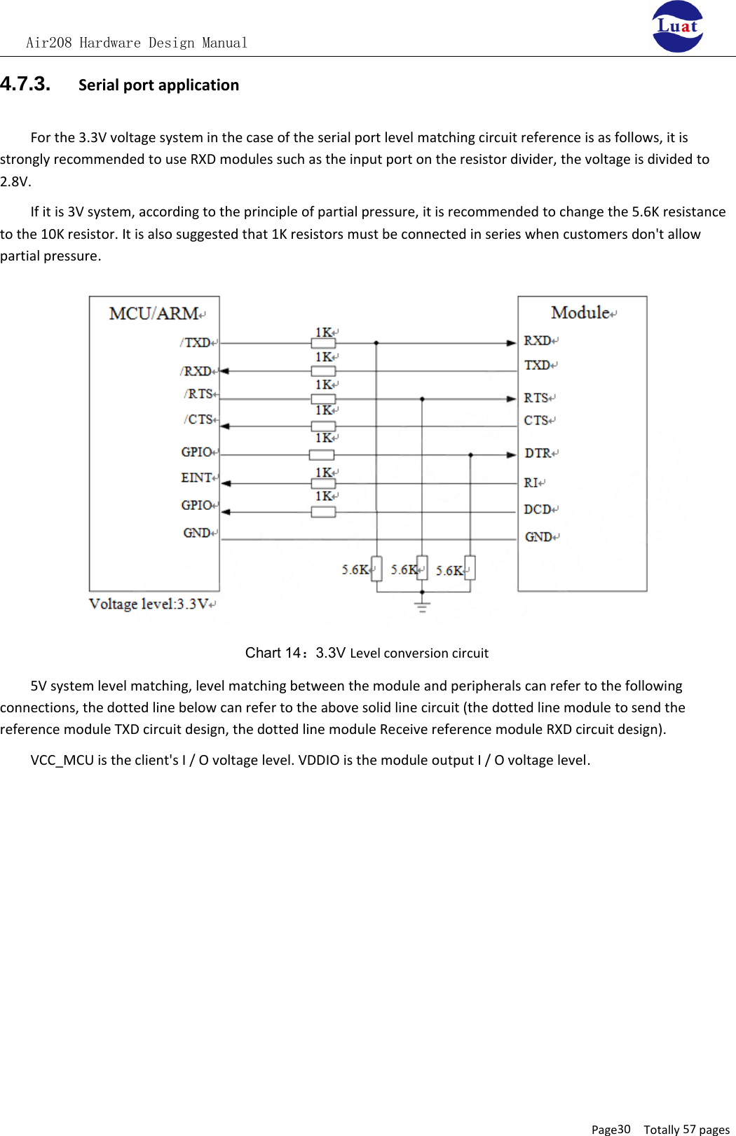
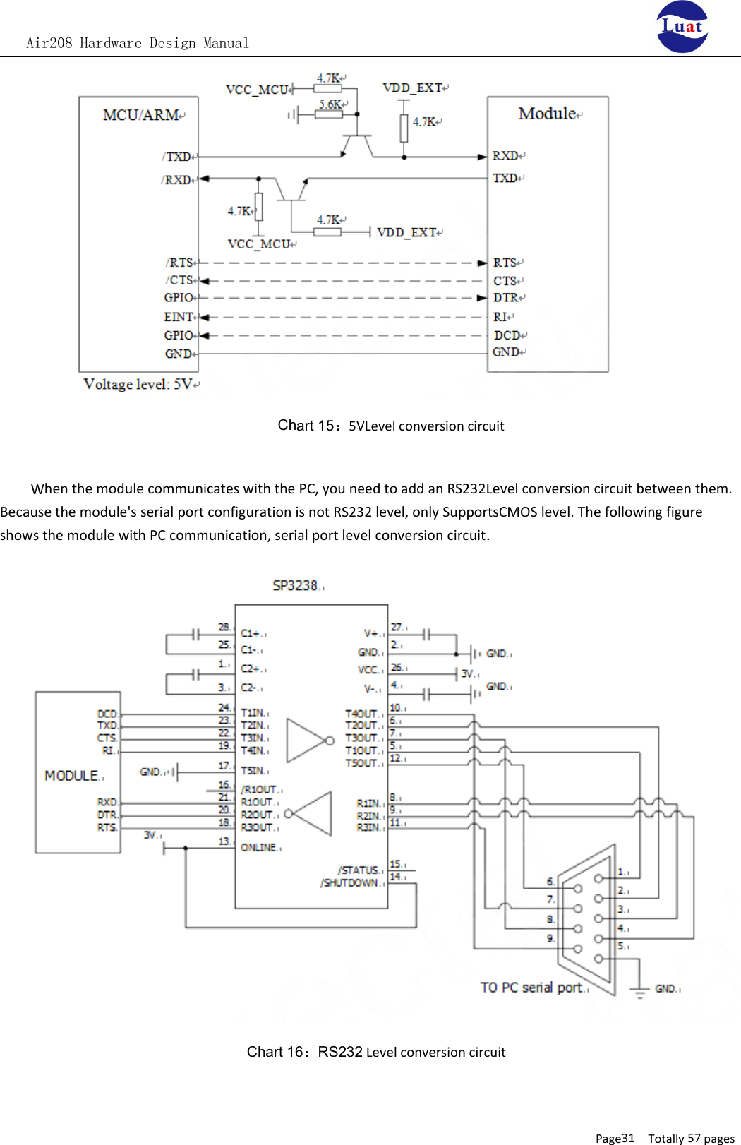
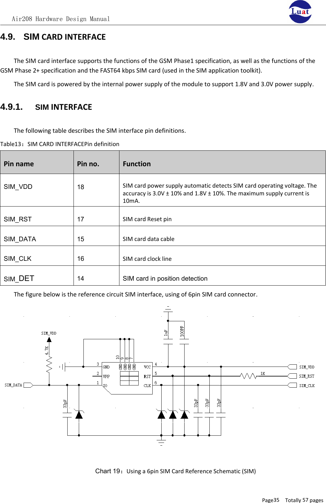
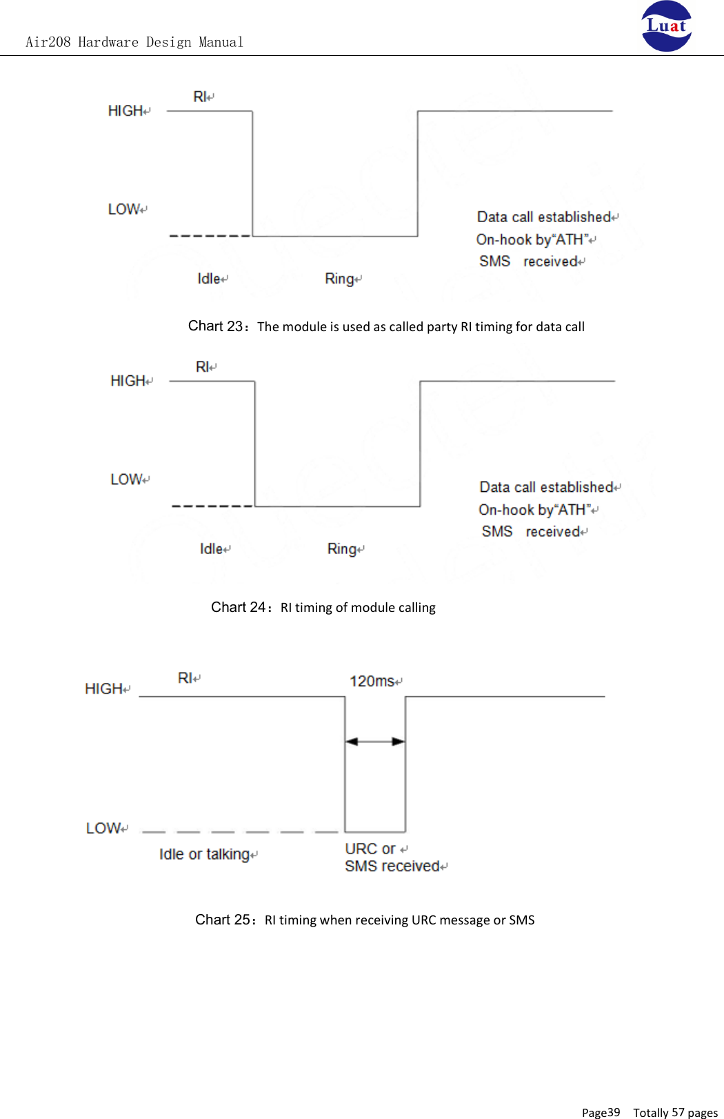
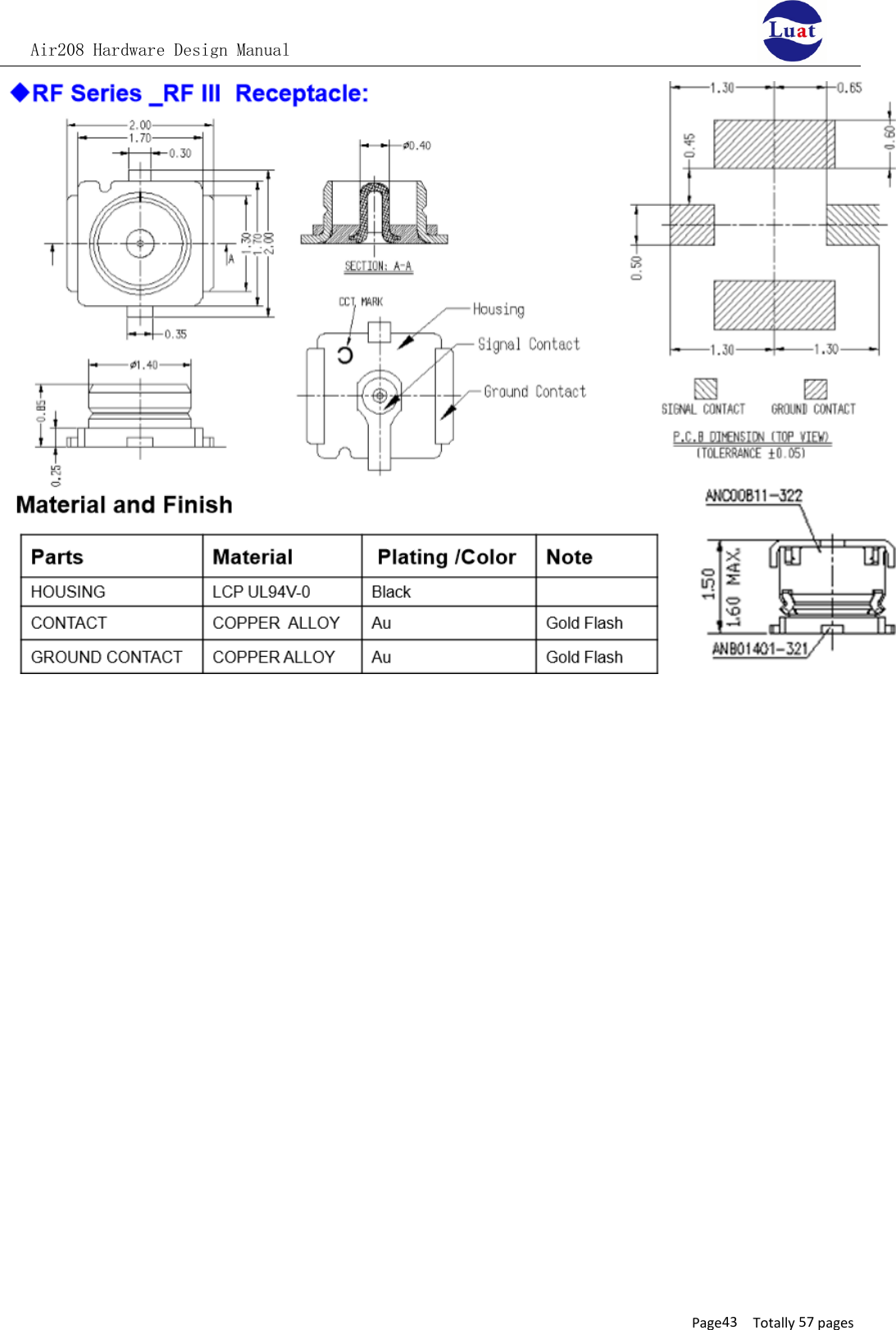
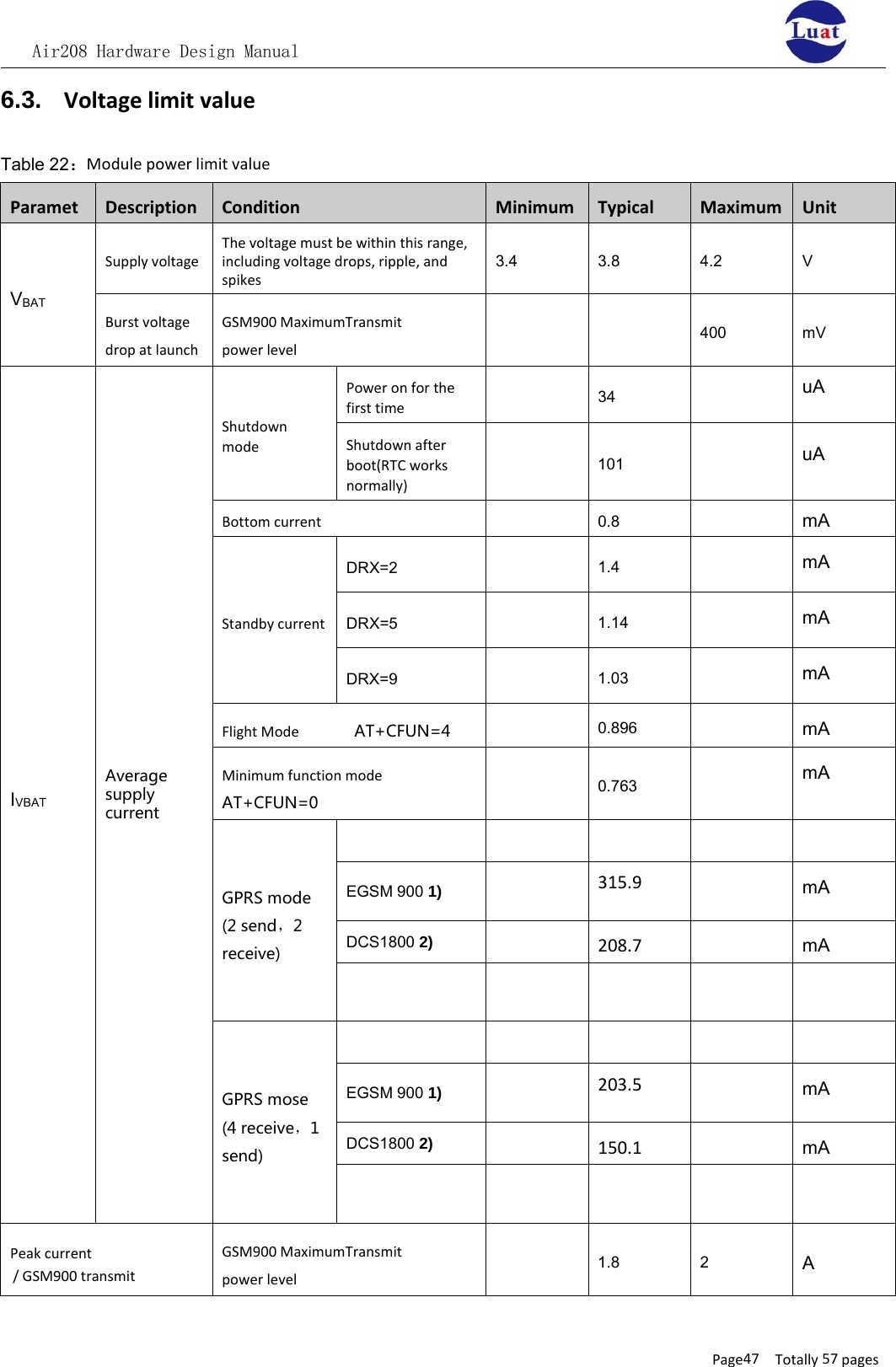
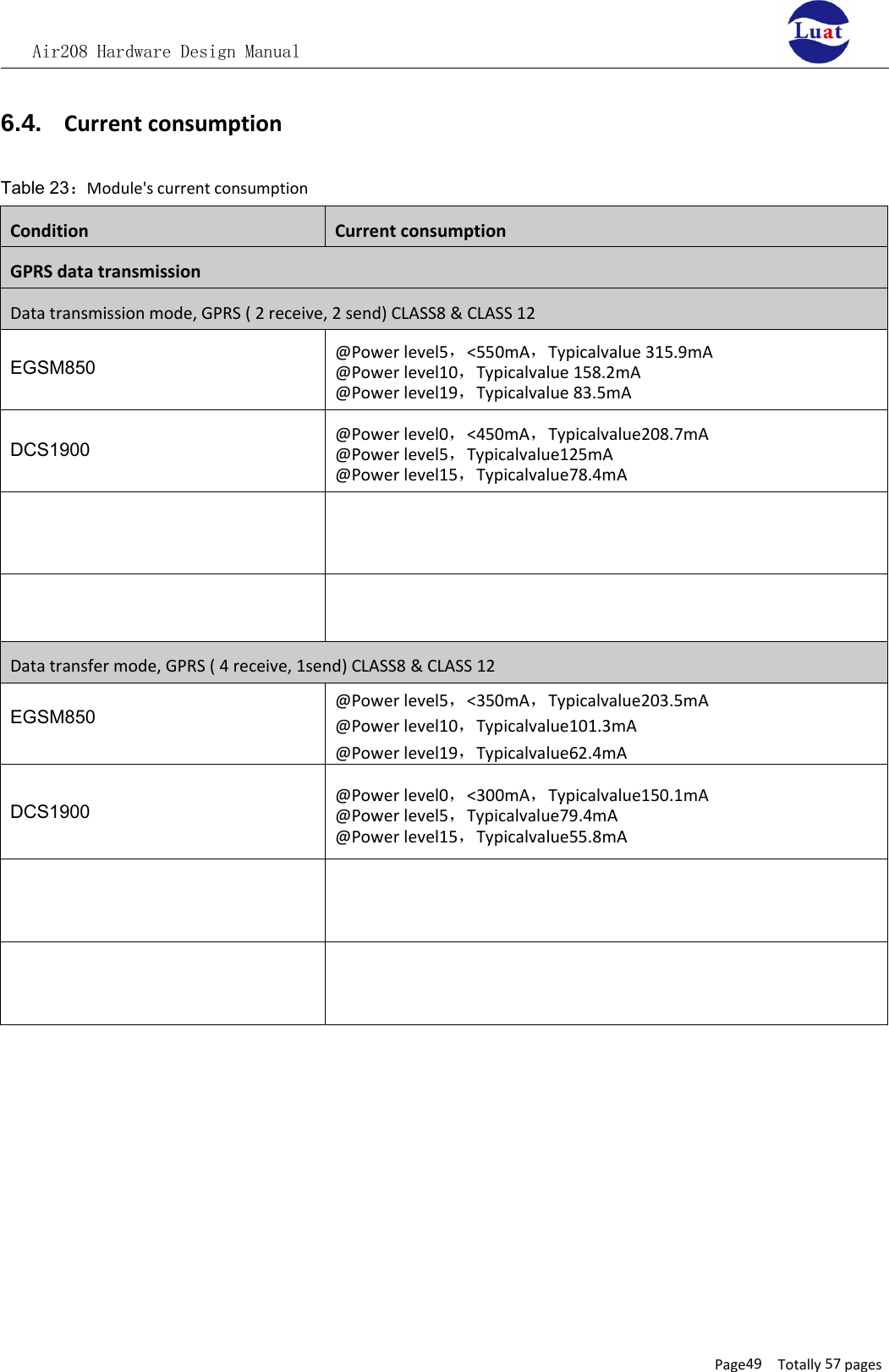
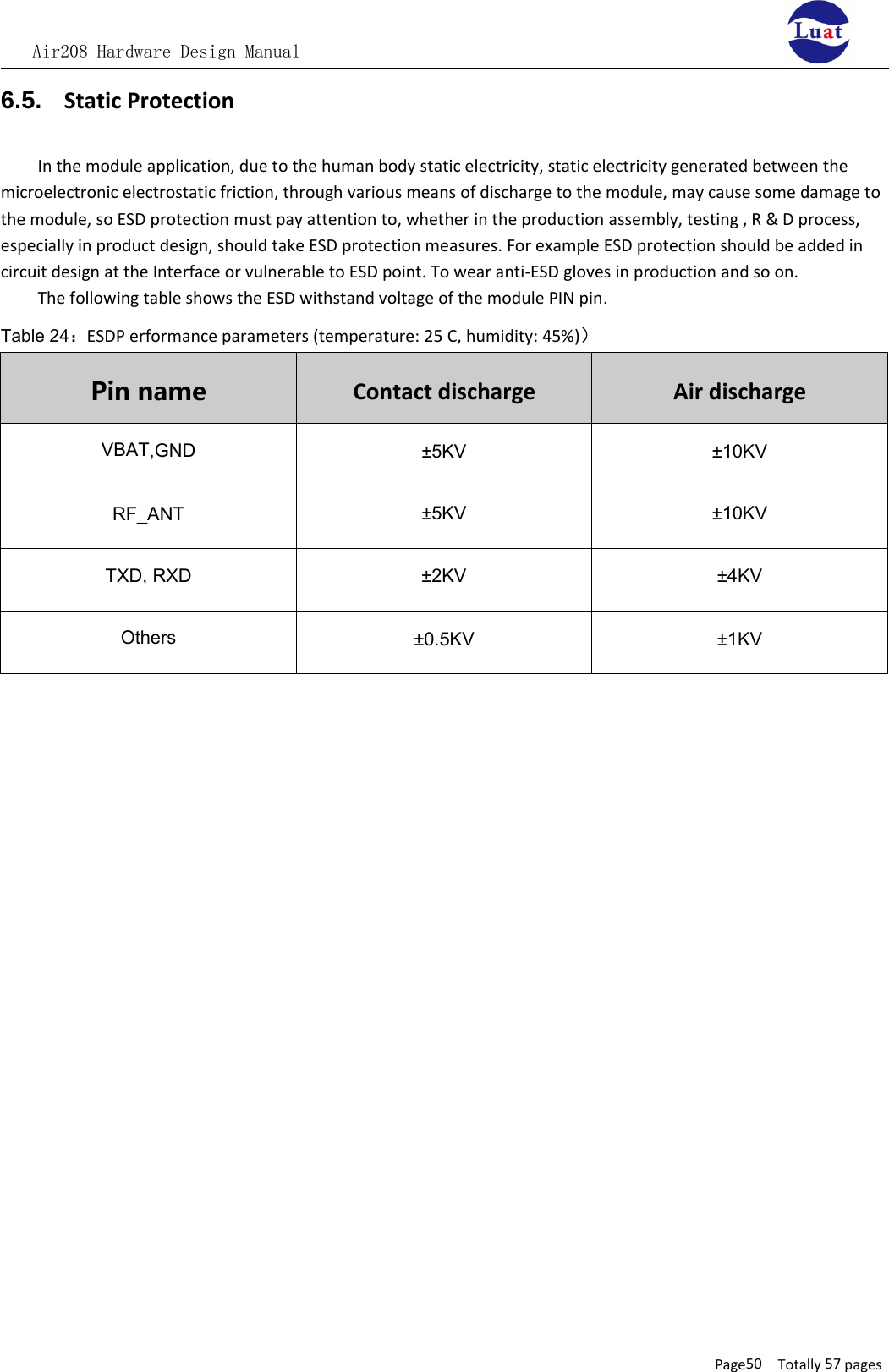
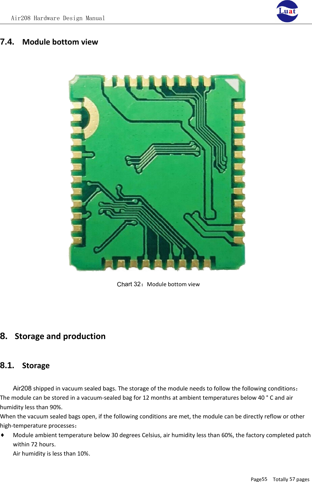
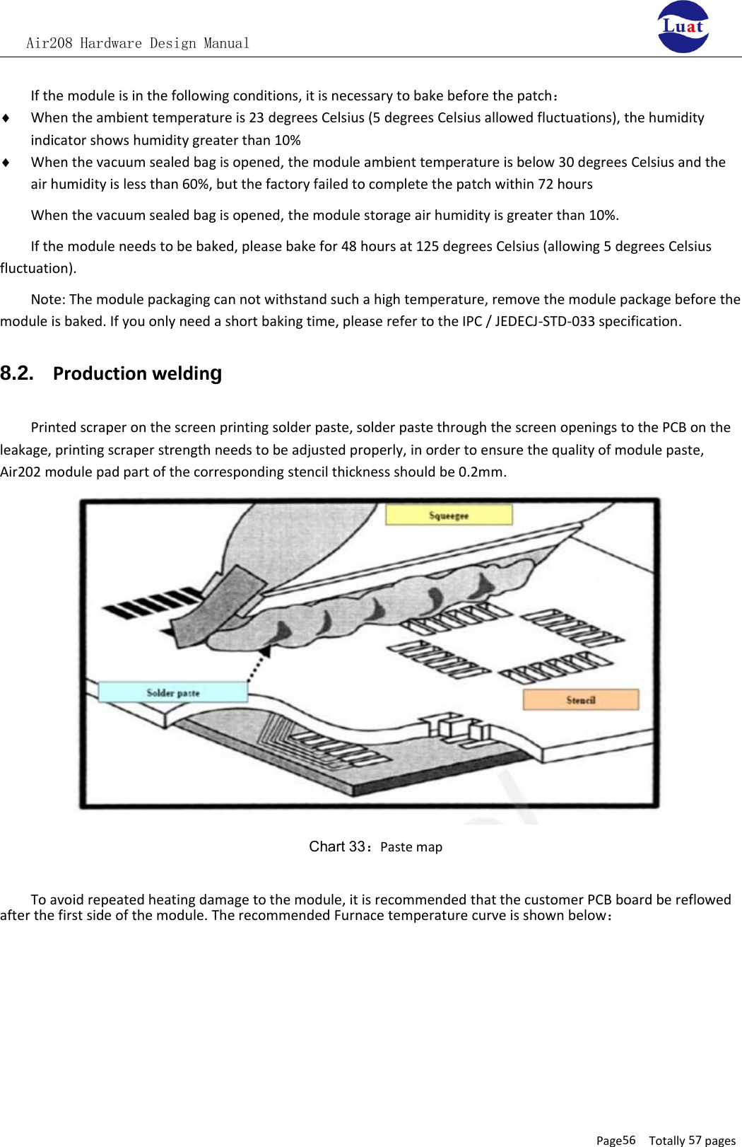
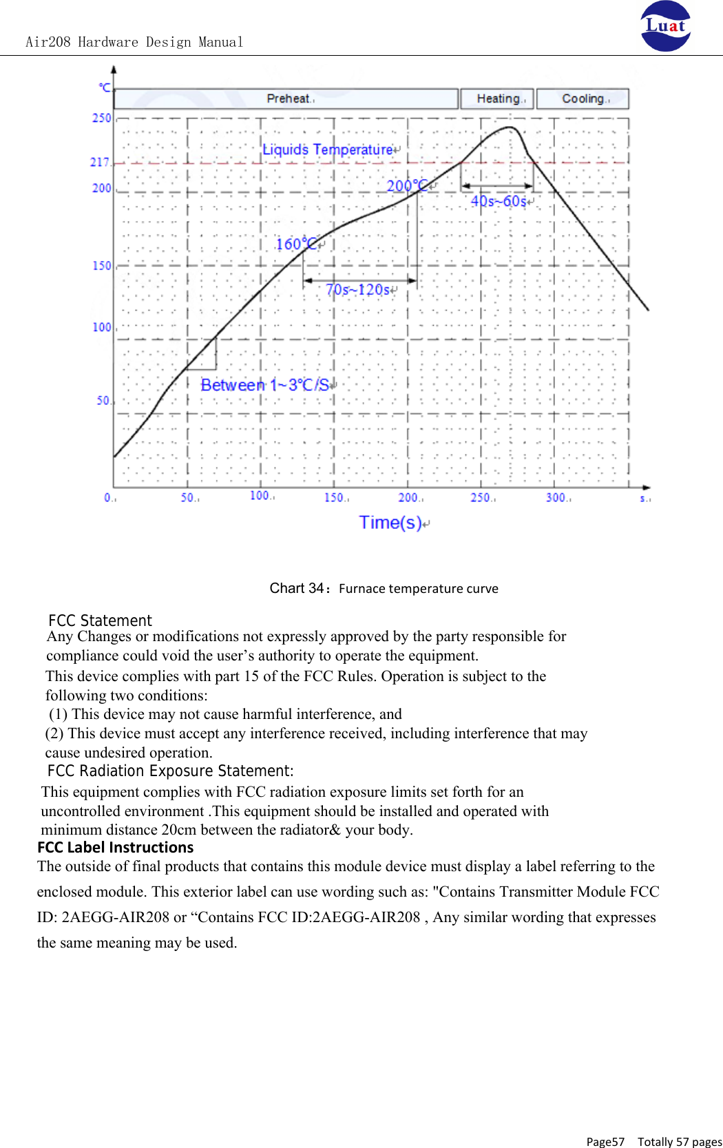
![Air208 Hardware Design ManualPage26 Totally 57 pages♦By default, the hardware flow control of the module is closed. When the client needs hardware flow control, pinsRTS, CTS must be connected to the client, and the AT command "AT+IFC=2,2" can be used to open the hardwareflow control. The AT command "AT+IFC=0,0" can be used to shut down the flow control. Please refer todocument [AT])Auxiliary serial port UART2♦UART2_TXD:Send data to the serial port of DTE♦UART2_RXD:Receive data from serial port of DTE♦Serial logic level is shown as the following table:Table8:Serial logic levelParameter Minimum value Maximum value UnitVIL 00.25×VDDIOVVIH 0.75×VDDIO VDDIO +0.3 VVOL 00.15×VDDIO VVOH 0.85×VDDIO VDDIO VTable 9:Definition of serial port pinsInterface Name pinFunctionMain serial portUART1UART1_DTR 12 DTE is readyUART1_TXD 8 Send data by serial portUART1_RXD 9 Serial port receives dataUART1_CTS 6 Clear sendUART1_RTS 7 DTE requests to send dataUART1_DCD 10 Carrier detectionUART1_RI 11 Ringing indicationAuxiliaryserial portUART2UART2_RXD 27 Serial port receives dataUART2_TXD 28 Serial port sends data](https://usermanual.wiki/AirM2M-Communication-Technology/AIR208/User-Guide-3829903-Page-26.png)