AirM2M Communication Technology AIR208 GSM/GPRS Module User Manual
Shanghai AirM2M Communication Technology Co., Ltd GSM/GPRS Module
User Manual
Air208_Hardware Design Manual_V1.03

Air208 Hardware Design Manual
Page2Totally 57 pages
Version
number
Modify record Date Date
V1.0 Newly build 2017‐8‐10 jinyi
V1.01 Modifies the main serial port on baud rate training content 2017‐9‐16 Guowen
V1.02 Adds pin description of the boot key booting and shutdown
machine
2017‐11‐03 Guowen
V1.03 Updates pin diagram 2017‐12‐13 Loukanghua

Air208 Hardware Design Manual
Page3Totally 57 pages
Catalog
1. TABLE CATALOG ............................................................................................................................................................ 6
2.1. RELATED DOCUMENTS.............................................................................................................................................................7
3. SUMMARY................................................................................................................................................................................ 8
3.1. FUNCTION CHART.................................................................................................................................................................10
3.2. EVALUATION BOARD.......................................................................................................................................................11
4. APPLICATION INTERFACE....................................................................................................................................................... 11
4.1. PIN DESCRIPTION..................................................................................................................................................................12
4.2. WORKING MODE..................................................................................................................................................................18
4.3. POWER SUPPLY....................................................................................................................................................................19
4.3.1. Module power supply working characteristics........................................................................................................19
4.3.2. Reduce voltage drop................................................................................................................................................19
4.3.3. Power supply reference circuit.................................................................................................................................20
4.4. BOOT AND SHUTDOWN......................................................................................................................................................... 21
4.4.1. Boot..........................................................................................................................................................................21
4.4.2. Shutdown.................................................................................................................................................................22
4.5. POWER SAVING TECHNOLOGY.................................................................................................................................................24
4.5.1. Least functional mode.............................................................................................................................................24
4.5.2. Sleep Mode (Slow Clock Mode
)
.............................................................................................................................24
4.5.3. Sleep wake...............................................................................................................................................................25
4.6. MODE SWITCHING SUMMARY................................................................................................................................................25
4.7. SERIAL PORT....................................................................................................................................................................... 25
4.7.1. Main serial port....................................................................................................................................................... 27
4.7.2. Debug serial port..................................................................................................................................................... 29
4.7.3. Serial port application............................................................................................................................................. 30
4.8. AUDIO INTERFACE................................................................................................................................................................ 32
4.8.1. Preventing TDD noise and other noises...................................................................................................................32
4.8.2. Microphone interface reference circuit................................................................................................................... 33
4.8.3. Audio output interface reference circuit..................................................................................................................33
4.8.4.
Audio Electrical characteristics
................................................................................................................. 34
4.9. SIM CARD INTERFACE.....................................................................................................................................................35
4.9.1. SIM INTERFACE....................................................................................................................................................... 35
4.9.2. 6-pin SIM card holder.............................................................................................................................................36
4.10. RI SIGNAL ACTION........................................................................................................................................................ 38
4.11. NETWORK STATUS INDICATION.............................................................................................................................................40
4.12. PWM.............................................................................................................................................................................41
5. RADIO INTERFACE...................................................................................................................................................................41
5.1. RF REFERENCE CIRCUIT..........................................................................................................................................................42
5.2. RF CONDUCTION SENSITIVITY........................................................................................................................................ 44

Air208 Hardware Design Manual
Page4Totally 57 pages
5.3. RECOMMENDED RF WELDING METHOD....................................................................................................................................45
6. ELECTRICAL CHARACTERISTICS, RELIABILITY, RF CHARACTERISTICS....................................................................................46
6.1. ABSOLUTE MAXIMUM...........................................................................................................................................................46
6.2. WORKING TEMPERATURE....................................................................................................................................................... 46
6.3. VOLTAGE LIMIT VALUE...........................................................................................................................................................47
6.4. CURRENT CONSUMPTION.......................................................................................................................................................49
6.5. STATIC PROTECTION............................................................................................................................................................. 50
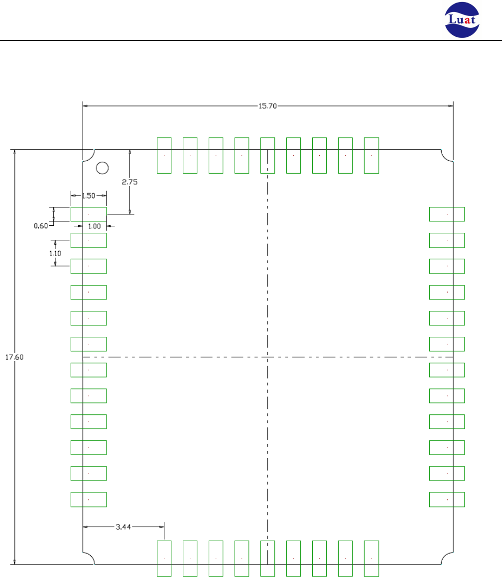
7. PHYCIAL DIMENSION..............................................................................................................................................................51
7.1. MODULE PHYCIAL DIMENSION................................................................................................................................................ 52
7.2. RECOMMENDED PCB ENCAPSULATION.................................................................................................................................... 53
7.3. MODULE FRONT VIEW...........................................................................................................................................................54
7.4. MODULE BOTTOM VIEW........................................................................................................................................................55
8. STORAGE AND PRODUCTION.................................................................................................................................................55
8.1. STORAGE............................................................................................................................................................................ 55
8.2. PRODUCTION WELDING.........................................................................................................................................................56

Air208 Hardware Design Manual
Page5Totally 57 pages
Chart Catalog
CHART 1 :FUNCTIONAL BLOCK DIAGRAM.................................................................................................10
CHART 2 :PIN ARRANGEMENT (FRONT VIEW)................................................................................. ...............12
CHART 3 :VOLTAGE AND CURRENT WAVEFORMSOFMODULE EMISSION
........................................................... 19
CHART 4 :VBAT INPUT REFERENCE CIRCUIT.............................................................................................20
CHART 5 :POWER INPUT REFERENCE DESIGN....................................................................................................21
CHART 6 :OPEN SET DRIVER REFERENCE BOOT CIRCUIT........................................................................................22
CHART 7 :BUTTON BOOTREFERENCE CIRCUIT............................................................................................... ......22
CHART 8 :OPEN DRIVER REFERENCE EMERGENCY SHUTDOWN CIRCUIT.....................................................................23
CHART 9 :BUTTON EMERGENCY SHUTDOWNREFERENCE CIRCUIT.............................................................................24
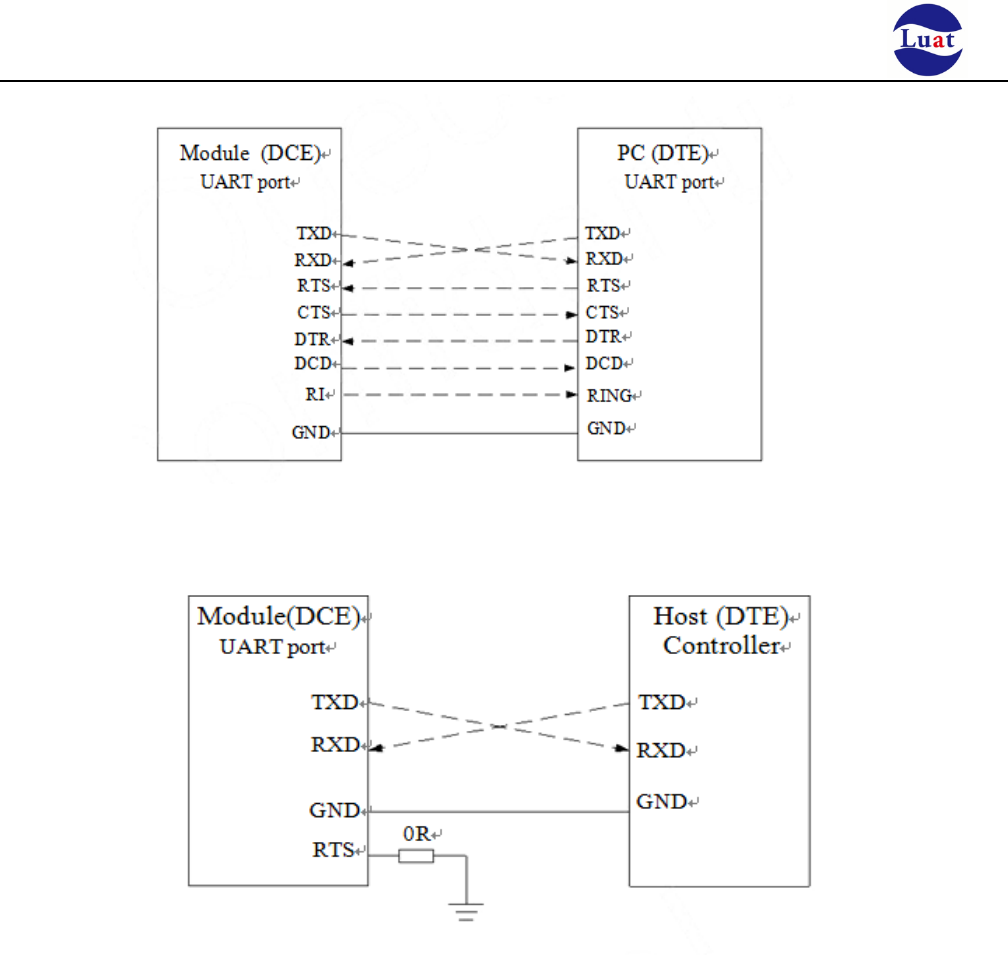
CHART 10 :FULL‐FEATURED SERIAL PORT CONNECTION DIAGRAM ...........................................................................28
CHART 11 :SERIAL THREE‐WIRE CONNECTION DIAGRAM.........................................................................................28
CHART 12 :SCHEMATIC DIAGRAM OF SERIAL CONNECTION MODE WITH FLOW CONTROL...............................................29
CHART 13 :SOFTWARE DEBUGGING CONNECTION DIAGRAM....................................................................................29
CHART 14 :3.3V LEVEL CONVERSION CIRCUIT......................................................................................................30
CHART 15 :5VLEVEL CONVERSION CIRCUIT...........................................................................................................31
CHART 16 :RS232 LEVEL CONVERSION CIRCUIT....................................................................................................31
CHART 17 :AIN MICROPHONE CHANNEL INTERFACE CIRCUIT.......................................................................33
CHART 18 :REFERENCE LINE................................................................................................................................34
CHART 19 :USING A 6PIN SIM CARD REFERENCE SCHEMATIC (SIM).........................................................................35
CHART 20 :WITH THE DETECTION OF PIN SIM CARD REFERENCE CIRCUIT DIAGRAM....................................36
CHART 21 :AMPHENOL C707 10M006 512 2 SIMCASSETTE..............................................................................37
CHART 22 :THE MODULE IS USED AS CALLED PARTY RI TIMING FOR VOICE CALL............................................................38
CHART 23 :THE MODULE IS USED AS CALLED PARTY RI TIMING FOR DATA CALL.............................................................39
CHART 24 :RI TIMING OF MODULE CALLING...........................................................................................................39
CHART 25 :RI TIMING WHEN RECEIVING URC MESSAGE OR SMS...............................................................................39
CHART 26 :NETLIGHTREFERENCE CIRCUIT.........................................................................................................40
CHART 27 :RF REFERENCE CIRCUIT.........................................................................................................................42
CHART 28 :SUGGESTION ON RF WELDING METHOD...................................................................................................45
CHART 29 :AIR208 FRONT VIEW (UNIT: MM).......................................................................................................52
CHART 30 :RECOMMENDED ENCAPSULATION (UNIT: MM)..........................................................................................53
CHART 31 :MODULE FRONT VIEW...........................................................................................................................54
CHART 32 :MODULE BOTTOM VIEW.........................................................................................................................55
CHART 33 :PASTE MAP.................................................................................................................................... ......56
CHART 34 :FURNACE TEMPERATURE CURVE................................................................................................................57

Air208 Hardware Design Manual
Page6Totally 57 pages
1. Table Catalog
TABLE 1:RELATED DOCUMENTS..................................................................................................................................................... 7
TABLE 2:MAINFEATURESOFTHEMODULE
......................................................................................................................................8
TABLE 3:AIR208 PIN ALLOCATION..............................................................................................................................................13
TABLE 4:PIN DESCRIPTIO............................................................................................................................................................14
TABLE5:GPIO CONFIGURATION TABLE............................................................................................................................................17
TABLE 6:WORK MODE...............................................................................................................................................................18
TABLE 7:MODE SWITCHING SUMMARY.........................................................................................................................................25
TABLE8:SERIAL LOGIC LEVEL..........................................................................................................................................................26
TABLE 9:DEFINITION OF SERIAL PORT PINS.....................................................................................................................................26
TABLE10 :AUDIO INTERFACEPIN DEFINITION.....................................................................................................................................32
TABLE 11 :TYPICAL CHARACTERISTICS OF ELECTRET MICROPHONES.....................................................................................................34
TABLE 12 :AUDIO INTERFACETYPICAL CHARACTERISTIC PARAMETERS.................................................................................................. 34
TABLE13 :SIM CARD INTERFACEPIN DEFINITION...........................................................................................................................35
TABLE 14 :RI SIGNAL ACTION.................................................................................................................................................38
TABLE 15 :NET_LED WORKING STATUS.....................................................................................................................................40
TABLE 16 :RF_ANTPIN DEFINITION...........................................................................................................................................41
TABLE 17 :RFCONDUCTION POWER.............................................................................................................................................44
TABLE 18 :RF CONDUCTION SENSITIVITY...............................................................................................................................44
TABLE 19 :MODULE WORKING FREQUENCY....................................................................................................................................45
TABLE20 :ABSOLUTE MAXIMUM.................................................................................................................................................... 46
TABLE 21 :WORKING TEMPERATURE..............................................................................................................................................46
TABLE 22 :MODULE POWER LIMIT VALUE...................................................................................................................................... 47
TABLE 23 :MODULE'S CURRENT CONSUMPTION..............................................................................................................................49
TABLE 24 :ESDP ERFORMANCE PARAMETERS (TEMPERATURE:25C,HUMIDITY:45%))................................................................50

Air208 Hardware Design Manual
Page7Totally 57 pages
2. Introduction
This document defines the Air208 module and hardware interface specification, electrical and mechanical details.
With the help of this document, combining with the application manual and user guide, customers can quickly apply
Air208 module for wireless applications.
2.1. Related documents
Table 1:Related documents
Item File name Remarks
1Detailed explanation of Air208_AT instruction set Has been published
2Air208 Reference design Has been published
3 Air208 module encapsulation Has been published
4Luat_AIR2XXupgradingtool1.1 Has been published
5Trace
Reference design Has been published
6 LuaForWindows_v5.1.5‐51 Has been published
7 Coolwatcher debugging tools and instructions _V1.1 Has been published
8 Platform compilation environment and installation steps Has been published
9 CSDTK3.7_Cygwin1.5.25_Svn_1.5.4_Full_Setup Has been published

Air208 Hardware Design Manual
Page8Totally 57 pages
3. Summary
Air208module is the two band GSM/GPRS module, its working frequency bands are:
GSM850MHz, WC^ϭ900MHz. Air208 supports GPRS multi slot level 12 and GPRS encoding formats
CS‐1, CS‐2, CS‐3andCS‐4.
With the ultra small size of 17.6mm * 15.7mm * 2.3mm, Air208 is able to meet all the needs of M2M,
including cars and personal tracking services, wireless POS, smart metering, industrial PDA and other M2M
applications.
Air208 is built‐in 32MbNorFlash + 32MbSRAM.
Air208 is a chip‐on‐module, with a LCC package that can be embedded in customer applications with its
pin‐on‐land, providing a rich hardware interface between the module and the customer's motherboard.
Air208 module uses a power‐saving technology, current consumption in sleep mode DRX = 5, as low as 1.14mA.
Air208 embeds protocols such as TCP UDP PPP HTTPS SSL and built‐in extended AT commands to make it easier
for users to use these Internet protocols.
Air208 complies with the RoHS standard.
Table 2:Main features of the module
Feature Description
Band
♦Quad‐band:GSM850,3CSϭϵϬϬ
♦Automatic frequency band search
♦Band selection can be set by AT command
♦Meets GSM Phase 2/2+
Transmitting power
♦Class4 (2W):
♦Class 1 (1W):
Power supply ♦DC 3.8V
Power saving mode
current consumption
♦1.40mA@DRX=2
♦1.14 mA@ DRX=5
♦1.03 mA@ DRX=9
GPRS Connection
characteristic
♦GPRS multi slot level is 12 (default)
♦GPRS mobile level B
GSM850
WCS1ϵ00

Air208 Hardware Design Manual
Page9Totally 57 pages
GPRS Data
characteristics
♦Downlink GPRS data transmission: maximum 85.6 kbps
♦GPRS data uplink transmission: maximum 85.6 kbps
♦Coding format:CS‐1,CS‐2,CS‐3andCS‐4
♦Support PAP (cryptographic authentication protocol) protocols commonly used for
PPP connections
♦Embedded protocol:TCP/UDP/FTP/PPP and so on
Temperature range
♦Normal working temperature:‐40°C ~ +85°C
♦storagetemperature:‐45°C ~ +90°C
SMS Text and PDU modes
SIM CARD INTERFACE SupportsSIM/USIM card:1.8V,3V
Characteristic 50 Ω
Audio interface Supports call, recording and playback function, can directly drive 8 ohm horn
Serial port
♦Full function serial port
For AT command and GPRS data
Adaptive baud rate:From 2400 bps to 921600 bps
♦Debug serial port
For software upgrade
For software debugging
Real time clock
Dimension
Real time clock
17.6×15.7×2.3mm
Weight:1.25g
Air208 Hardware Design Manual
Page10 Totally 57 pages
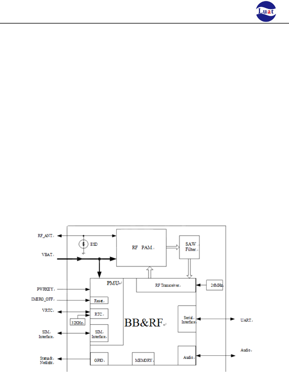
3.1. Function Chart
Following is Air208Functional block diagram,describing its main function:
♦storage
♦GSM RF
♦Power Management
♦Interface section
— SIM card interface
—Audio interface
— UART interface
— Power supply
—RF interface
— Boot and shutdown
Chart 1:Functional block diagram

Air208 Hardware Design Manual
Page11 Totally 57 pages
3.2. Evaluation Board
In order to help test and use Air208, Airm2m provides a set of evaluation boards. They includes Air208 module,
EVB_Air208, UART to USB cable and so on.
4. Application interface
The module uses LCC package, 42 SMT welding coil pins, and the following chapter details the functions o
f
the
following interfaces:
♦power supply (refer to power supply section)
♦Switch machine (refer to switch section)
♦power saving technology (refer to power saving technology section)
♦Serial port (refer to serial section)
♦Audio interface(refer to audio section)
♦SIM CARD INTERFACE(refer to SIM card section)
Air208 Hardware Design Manual
Page12 Totally 57 pages
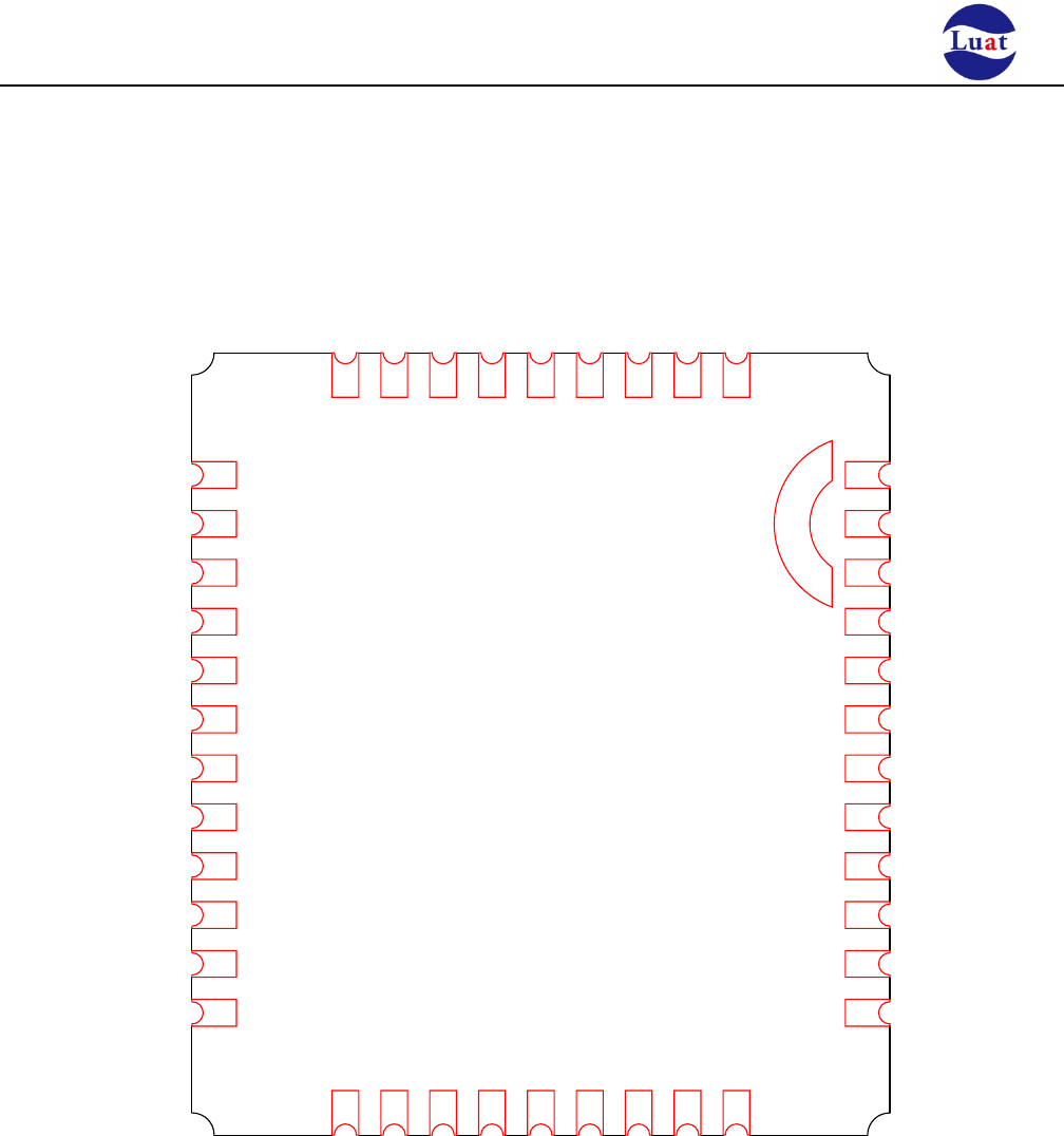
4.1. Pin description
GND 13
SIM_DET 14
SIM_DAT 15
SIM_CLK 16
SIM_RST 17
SIM_VDD 18
GND 19
RESET 20
GND 21
UART1_TXD 1
UART1_RXD 2
UART1_RTS 3
UART1_CTS 4
UART1_DCD 5
UART1_DTR 6
UART1_RI 7
GND 8
MICP 9
MICN 10
SPKP 11
SPKN 12
33 GND
32 ANT
31 GND
30 GND
29 GPIO_6
28 VRTC
27 GND
26 HOST_TXD
25 HOST_RXD
24 CHG_DET
23 UART2_RXD
22 UART2_TXD
42 STATUS
41 NET_LED
40 VDDIO
39 PWRKEY
38 ADC
37 GND
36 GND
35 VBAT
34 VBAT
Air208
Chart 2:Pin arrangement (front view)

Air208 Hardware Design Manual
Page13 Totally 57 pages
Table 3:Air208 Pin allocation
Pin Pin name Input/Output Pin No. Pin name Input/Output
1UART1_TXD/GPIO_1 I22 UART2_TXD/GPIO_5 O
2 UART1_RXD/GPIO_0 O23 UART2_RXD/GPIO_4 I
3UART1_RTS/GPIO_2O24 CHG_DET I
4UART1_CTS/GPIO_3I25 HOST_RXD I
5 UART1_DCD/GPIO_31 O26 HOST_TXD O
6 UART1_DTR/GPIO_29 I27 GND
7 UART1_RI/GPIO_30 O28 GPIO_6 I/O
8GND 29 VRTC I
9MICP I30 GND
10 MICN I31 GND
11 SPKP O32 ANT I/O
12 SPKN O33 GND
13 GND 34 VBAT I
14 SIM_DET/GPIO_7 I35 VBAT I
15 SIM_DAT I/O 36 GND
16 SIM_CLK I/O 37 GND
17 SIM_RST O38 ADC I
18 SIM_VDD O39 PWRKEY I
19 GND 40 VDDIO O
20 RESET I41 NET_LED/GPIO_33 O
21 GND 42 STATUS/GPIO_11 O
Air208 Hardware Design Manual
Page14 Totally 57 pages
Table 4:Pin descriptio
owerSupply
Pin name Pin No. I/O Pin description Electrical characteristics Remark
VBAT 34 35 I Module's main power
supplyVBAT=3.4V~4.2
V
Vmax= 4.2V
Vmin=3.4V
Vnorm=3.8V
The module has a
maximum load current
of 1.6A in burst mode
VDDIO 41 O Output 2.8V,10mA Vmax=2.95V
1.Hang when not in
usage
2.Ifthispinisusedfor
external power supply,
it is recommended to
shunt a 2~4.7uF
decoupling capacitor,
and the load current
should not exceed
10mA
GND
81319
21 27
30 31
33 36
Module GND
Power button
Pin name Pin no. I/O Pin description Electrical characteristics Remark
PWRKEY 39 I Internal pull‐up, pull the pin
lower than 1.5s module
boot
VILmax=0.4V
RESET 20 I
Hardware shutdown pin,
active low。The module
shutdown after pulldown
more than 200ms
Vmax= 1.5V
Vmin=1.1V
Vnorm=1.35V
No external pull‐ups are
required
Audio interface
Pin name Pin no. IPin description Electrical characteristics Remark
MICP
MICN 9
10 IDifferential audio input
SPKP
SPKN 11 12 O Differential audio output,
you can directly drive the 8
ohm speaker
The main serial port
Pin name Pin no. I/O Pin description Electrical characteristics Remark

Air208 Hardware Design Manual
Page15 Totally 57 pages
UART1_TXD
(GPIO_1)
(SPI2_CS0) 1OModule to send data
VILmin=-0.3V
VILmax=0.25×VDDIO
VIHmin=0.75×VDDIO
VIHmax=VDDIO+0.3
VOHmin=0.85×VDDIO
VOLmax=0.15×VDDIO
RXD needs external 10K
ohm resistor to pull to
VDDIO.
If communication is
used only in TXD, RXD
and GND, it is
recommended that RTS
be grounded through
10K ohm resistance;
The module defaults to
sleep and power saving.
If you want to send AT
instructions to the
module during
hibernation, you need
to lower the DTR to
wake up the module;
If you do not want the
moduletogotosleep,
you can ground the DTR
through a 10K resistor.
Other pins can be hang
when is not in usage.
UART1_RXD
(GPIO_0)
(SPI2_CLK) 2I
The module receives the
data
UART1_CTS
(GPIO_3)
(SPI2_DO) 4OClear send
UART1_RTS
(GPIO_2)
(SPI2_CS1) 3I
The DTE requests to send
data to the module
UART1_DTR
(GPIO_29) 6I
DTEisready
UART1_DCD
(GPIO_31) 5O
Carrier detection (this pin
represents the
communication link)
UART1_RI
(GPIO_30) 7O
Module output ringing hint
UART2
Pin name Pin no. I/O Pin description Electrical characteristics Remark
UART2_RXD
(GPIO_4)
(SPI2_DI)
(LPG)
23 I
Hardeare UART2
VILmin=-0.3V
VILmax=0.25×VDDIO
VIHmin=0.75×VDDIO
VIHmax=VDDIO+0.3
VOHmin=0.85×VDDIO
VOLmax=0.15×VDDIO
Hang when not in usage
UART2_TXD
(GPIO_5)
(PWM) 22 O
Debug serial port
Pin name Pin no. I/O Pin description Electrical characteristics Remark
HOST_RXD 25 I
For software debugging and
firmware download
VILmin=-0.3V
VILmax=0.25×VDDIO
VIHmin=0.75×VDDIO
VIHmax=VDDIO+0.3
VOHmin=0.85×VDDIO
VOLmax=0.15×VDDIO
Hang when not in usage
HOST_TXD 26 O
SIM CARD INTERFACE
Pin name Pin no. I/O Pin description Electrical characteristics Remark
SIM_VDD 18 O Power supply voltage of
SIM card
Themoduleautomatically
selects 1.8V or 3.0V
SIM CARD INTERFACEIt
is recommended to use
TV
S
tube
f
o
rE
S
D

Air208 Hardware Design Manual
Page16 Totally 57 pages
SIM_RST 17 O SIMcard Reset
3V:
VOLmax=0.36
VOHmin=0.9×SIM_VDD
1.8V:
VOLmax=0.2×SIM_VDD
VOHmin=0.9×SIM_VDD
SIM_DAT 15 I/O SIM card data cable
3V:
VOLmax=0.4
VOHmin= SIM_VDD-0.4
1.8V:
VOLmax=0.15×SIM_VDD
VOHmin=SIM_VDD-0.4
SIM_CLK 16 O SIM card clock cable
3V:
VOLmax=0.4
VOHmin=0.9×SIM_VDD
1.8V:
VOLmax=0.12×SIM_VDD
VOHmin=0.9×SIM_VDD
SIM_DET
(GPIO_7)
(UART2_CTS)
(I2C_SDA)
14 ISIM card in position
detection VOHmin=0.85×VDDIO
VOLmax=0.15×VDDIO Hang when not in usage
ADC
Pin name Pin no. I/O Pin description Electrical characteristics Remark
ADC0 38 I Analog to digital
converter
Input range 0~1.85V
10bit
tolerance scope +—20mv Hang when not in usage
GPIO
Pin name Pin no. I/O Pin description Electricalcharacteristics Remark
NET_LED
(GPIO_33)
(32K_OUT) 41 ONetwork status
indication VOHmin=0.85×VDDIO
VOLmax=0.15×VDDIO Hang when not in
usage
STATUS
(GPIO_11) 42 OOperating status
detection VOHmin=0.85×VMMC
VOLmax=0.15×VMMC Hang when not in
usage
GPIO_6
(UART2_RTS)
(I2C_CLK) 29 I/O Reserved VOHmin=0.85×VDDIO
VOLmax=0.15×VDDIO Hang when not in
usage
Radio interface
Pin name Pin no. I/O Pin description Electrical characteristics Remark
ANT 32 I/O GPRS RF signal input and
output
50 ohm characteristic
impedance

Table5:GPIO Configuration table
Air208
PINNO.
GPIO
number
Name.
Power
Domain
Pull‐
Up
Pull‐
Up/Down
Resistor
At Reset After Reset Function0 Function1 Function2 Function3
H/L/Hiz pull PinState H/L/Hiz pull PinStateFunction0 Type PULL ADDRESS Function1 Type PULL ADDRESS Function2 Type PULL ADDRESS Function3 Type PULL ADDRESS
2G
PIO0GPIO_0/UART1_RXD
VDDIO
2.8V
2.8V, 166K HUPINPUT HUPINPUT GPIO_0 I/O UP 0x01A2A090(0x0) UART1_RXD I UP 0x01A2A090(0x1) SPI2_CLK I/O UP 0x01A2A090(0x2)
1GPIO1 GPIO_1/UART1_TXD 2.8V, 166K L DN INPUT L DN INPUT GPIO_1 I/O DN 0x01A2A094(0x0) UART1_TXD O OFF 0x01A2A094(0x1) SPI2_CS_0 I/O UP 0x01A2A094(0x2)
3GPIO2 GPIO_2/UART1_RTS 2.8V, 166K L DN INPUT L DN INPUT GPIO_2 I/O DN 0x01A2A098(0x0) UART1_RTS I UP 0x01A2A098(0x1) SPI2_CS_1 I/O UP 0x01A2A098(0x2) PWL_1 O OFF 0x01A2A098(0x3)
4GPIO_3 GPIO_3/UART1_CTS 2.8V, 166K L DN INPUT L DN INPUT GPIO_3 I/O DN 0x01A2A09C(0x0) UART1_CTS O OFF 0x01A2A09C(0x1) SPI2_DI_0 I/O DN 0x01A2A09C(0x2) LPSCO_1 O OFF 0x01A2A09C(0x3)
23 GPIO_4 GPIO_4/UART2_RXD 2.8V, 166K HUPINPUT HUPINPUT GPIO_4 I/O UP 0x01A2A0A0(0x0) UART2_RXD I UP 0x01A2A0A0(0x1) SPI2_DI_1 I UP 0x01A2A0A0(0x2) LPG O UP 0x01A2A0A0(0x3)
22 GPIO_5 GPIO_5/UART2_TXD 2.8V, 166K L DN INPUT L DN INPUT GPIO_5 I/O DN 0x01A2A0A4(0x0) UART2_TXD O OFF 0x01A2A0A4(0x1) LCD_TE I DN 0x01A2A0A4(0x2) PWT O OFF 0x01A2A0A4(0x3)
29 GPIO_6 GPIO_6/UART2_RTS/I2C3_SCL 2.8V, 33K L DN INPUT L DN INPUT GPIO_6 I/O DN 0x01A2A0A8(0x0) UART2_RTS I UP 0x01A2A0A8(0x1) I2C3_SCL I/O UP 0x01A2A0A8(0x2) TCO_3 O OFF 0x01A2A0A8(0x3)
14 GPIO_7 GPIO_7/UART2_CTS/I2C3_SDA 2.8V, 33K L DN INPUT L DN INPUT GPIO_7 I/O DN 0x01A2A0AC(0x0) UART2_CTS O OFF 0x01A2A0AC(0x1) I2C3_SDA I/O UP 0x01A2A0AC(0x2) TCO_4 O OFF 0x01A2A0AC(0x3)
\GPIO_8 SSD_CLK/SPI1_CLK
VMMC
1.8/1.9/2.0/2.6/2.8/3.0/3.3V
1.9V, 166K L OFF OUTPUT 26MHz OFF OUTPUT SDMMC_CLK O OFF 0x01A2A04C(0x0) GPIO_8 I/O DN 0x01A2A04C(0x1) SPI1_CLK I/O DN 0x01A2A04C(0x2) I2C1_SCL I/O UP 0x01A2A04C(0x3)
\ GPIO_9 SSD_CMD/SPI1_CS0 1.9V, 50K H UP INPUT H UP INPUT SDMMC_CMD I/O UP 0x01A2A050(0x0) GPIO_9 I/O DN 0x01A2A050(0x1) SPI1_CS_0 I/O UP 0x01A2A050(0x2) I2C1_SDA I/O UP 0x01A2A050(0x3)
\ GPIO_10 SSD_DATA0/SPI1_CS1 1.9V, 50K H UP INPUT H UP INPUT SDMMC_DATA_0 I/O UP 0x01A2A054(0x0) GPIO_10 I/O DN 0x01A2A054(0x1) SPI1_CS_1 I/O UP 0x01A2A054(0x2)
42 GPIO_11 SSD_DATA1/SPI1_DI_O 1.9V, 50K H UP INPUT H UP INPUT SDMMC_DATA_1 I/O UP 0x01A2A058(0x0) GPIO_11 I/O DN 0x01A2A058(0x1) SPI1_DI_0 I/O DN 0x01A2A058(0x2)
\ GPIO_12 SSD_DATA2/SPI1_DI_1 1.9V, 50K H UP INPUT H UP INPUT SDMMC_DATA_2 I/O UP 0x01A2A05C(0x0) GPIO_12 I/O DN 0x01A2A05C(0x1) SPI1_DI_1 I DN 0x01A2A05C(0x2)
\ GPIO_13 SSD_DATA3 1.9V, 50K H UP INPUT H UP INPUT SDMMC_DATA_3 I/O UP 0x01A2A060(0x0) GPIO_13 I/O DN 0x01A2A060(0x1)
\G
PIO_14GPIO_14/I2S_BCK
VLCD
1.8/2.8V
1.9V, 166K H OFF OUTPUT H OFF OUTPUT LCD_RSTB O OFF 0x01A2A064(0x0) GPIO_14 I/O DN 0x01A2A064(0x1) DAI_RST I DN 0x01A2A064(0x2) I2S_BCK I/O DN 0x01A2A064(0x3)
\ GPIO_15 GPIO_15/I2S_LRCK 1.9V, 166K H OFF OUTPUT H OFF OUTPUT SPI_LCD_CS O OFF 0x01A2A068(0x0) GPIO_15 I/O DN 0x01A2A068(0x1) DAI_CLK O OFF 0x01A2A068(0x2) I2S_LRCK I/O DN 0x01A2A068(0x3)
\ GPIO_16 GPIO_16/I2S_DI 1.9V, 166K H OFF OUTPUT H OFF OUTPUT SPI_LCD_SCK O OFF 0x01A2A06C(0x0) GPIO_16 I/O DN 0x01A2A06C(0x1) DAI_DI I DN 0x01A2A06C(0x2) I2S_DI I DN 0x01A2A06C(0x3)
\ GPIO_17 GPIO_17/I2S_DO 1.9V, 166K L DN OUTPUT L DN OUTPUT SPI_LCD_DIO I/O DN 0x01A2A070(0x0) GPIO_17 I/O DN 0x01A2A070(0x1) DAI_DO O OFF 0x01A2A070(0x2) I2S_DO O OFF 0x01A2A070(0x3)
\ GPIO_18 GPIO_18 1.9V, 166K H OFF OUTPUT H OFF OUTPUT SPI_LCD_SDC O OFF 0x01A2A074(0x0) GPIO_18 I/O DN 0x01A2A074(0x1)
\GPIO_19 GPIO_19/I2C2_SCL
VCAM
1.8/2.8V
1.9V, 33K H OFF OUTPUT H OFF OUTPUT CAM_PWDN O OFF 0x01A2A078(0x0) GPIO_19 I/O DN 0x01A2A078(0x1) I2C2_SCL I/O UP 0x01A2A078(0x2)
\ GPIO_20 GPIO_20/I2C2_SDA 1.9V, 33K L OFF OUTPUT L OFF OUTPUT CAM_RSTB O OFF 0x01A2A07C(0x0) GPIO_20 I/O DN 0x01A2A07C(0x1) I2C2_SDA I/O UP 0x01A2A07C(0x2)
\ GPIO_21 GPIO_21 1.9V, 166K L OFF OUTPUT L OFF OUTPUT CAM_CLK O OFF 0x01A2A080(0x0) GPIO_21 I/O DN 0x01A2A080(0x1)
\ GPIO_22 GPIO_22 1.9V, 166K H DN OUTPUT H DN OUTPUT SPI_CAM_SCK I/O DN 0x01A2A084(0x0) GPIO_22 I/O DN 0x01A2A084(0x1)
\ GPIO_23 GPIO_23 1.9V, 166K L DN INPUT L DN INPUT SPI_CAM_DI_0 I DN 0x01A2A088(0x0) GPIO_23 I/O DN 0x01A2A088(0x1) SPI_CAM_DI_1 I DN 0x01A2A088(0x2)
\ GPIO_24 GPIO_24 1.9V, 166K L DN INPUT L DN INPUT SPI_CAM_DI_1 I DN 0x01A2A08C(0x0) GPIO_24 I/O DN 0x01A2A08C(0x1) SPI_CAM_DI_0 I DN 0x01A2A08C(0x2) SPI_CAM_SSN I/O DN 0x01A2A08C(0x3)
\GPIO_25GPIO_25
VDDIO
2.8V
2.8V, 166K L DN INPUT L DN INPUT KEYIN_0 I DN 0x01A2A0B0(0x0) GPIO_25 I/O DN 0x01A2A0B0(0x1)
\ GPIO_26 GPIO_26 2.8V, 166K L DN INPUT L DN INPUT KEYIN_1 I DN 0x01A2A0B4(0x0) GPIO_26 I/O DN 0x01A2A0B4(0x1)
\ GPIO_27 GPIO_27 2.8V, 166K L DN INPUT L DN INPUT KEYIN_2 I DN 0x01A2A0B8(0x0) GPIO_27 I/O DN 0x01A2A0B8(0x1)
\ GPIO_28 GPIO_28 2.8V, 166K L DN INPUT L DN INPUT KEYIN_3 I DN 0x01A2A0BC(0x0) GPIO_28 I/O DN 0x01A2A0BC(0x1)
6GPIO_29 GPIO_29 2.8V, 166K L DN INPUT L DN INPUT KEYIN_4 I DN 0x01A2A0C0(0x0) GPIO_29 I/O DN 0x01A2A0C0(0x1)
7GPIO_30 GPIO_30 2.8V, 166K L DN INPUT L DN INPUT KEYOUT_0 I/O DN 0x01A2A0C4(0x0) GPIO_30 I/O DN 0x01A2A0C4(0x1)
5GPIO_31 GPIO_31 2.8V, 166K L DN INPUT L DN INPUT KEYOUT_1 I/O DN 0x01A2A0C8(0x0) GPIO_31 I/O DN 0x01A2A0C8(0x1)
\ GPIO_32 GPIO_32 2.8V, 166K L DN INPUT L DN INPUT KEYOUT_2 I/O DN 0x01A2A0CC(0x0) GPIO_32 I/O DN 0x01A2A0CC(0x1)
41 GPIO_33 GPIO_33/32K_OUT 2.8V, 166K L DN INPUT L DN INPUT KEYOUT_3 I/O DN 0x01A2A0D0(0x0) GPIO_33 I/O DN 0x01A2A0D0(0x1) DBG_CLK(32Kclockout) O OFF 0x01A2A0D0(0x5)
\ GPIO_34 GPIO_34 2.8V, 166K L DN INPUT L DN INPUT KEYOUT_4 I/O DN 0x01A2A0D4(0x0) GPIO_34 I/O DN 0x01A2A0D4(0x1) HST_CLK I DN 0x01A2A0D4(0x5)
25 GPIO_35 HST_RXD/GPIO_35 VDDIO
2.8V
2.8V, 166K H UP INPUT H UP INPUT HST_RXD I UP 0x01A2A0D8(0x0) GPIO_35 I/O DN 0x01A2A0D8(0x1)
26 GPIO_36 HST_TXD/GPIO_36 2.8V 166K H UP OUTPUT H UP OUTPUT HST_TXD I/O UP 0x01A2A0DC(0x0) GPIO_36 I/O DN 0x01A2A0DC(0x1)

4.2. Working mode
The table below briefly describes the various modes of work mentioned in the next few chapters.
Table 6:Work mode
Mode Function
Normal work
GSM/GPRS SLEEP
If the DTR pin is high and there is no interrupt (for example, GPIO interrupt or serial
data wake‐up interrupt), the module will automatically enter the sleep mode. Sleep
mode, the module is still able to receive packets, short messages and calls.
GSM IDLE Software running normally. Module registration on GSM network, no data, voice
and SMS interaction.
GSM TALK
GSM connection to work properly. Have data or voice or SMS interaction. In this
mode, the power consumption of the module depends on the strength of the
environmental signal, dynamic DTX control and the working frequency of the radio.
GPRS IDLE Module is not registered to GPRS network. Modules cannot be accessed through
GPRS channels.
GPRS STANDBY The module registers on the GPRS network, but does not activate the PDP context
(the module does not get the IP address).
GPRS READY The PDP context is successfully activated (the module has acquired the IP address),
but no data is transferred. In this state, the module can send or receive data.
GPRS DATA
GPRS data transfer. In this mode, the power dissipation of the module depends on
the power control level, the working RF frequency band and the GPRS multi slot
configuration.
Shutdown mode
By sending the "AT+CPOWD=1" command, using the PWRKEY pin or using "RESET" 1 "pins to achieve the
normal shutdown. The Power Supply management chip turns off the baseband power supply and retains only
the RTC power supply. The software is not running, the serial port can not access. Maintain VBATPower Supply
power supply.
Minimum
function mode
(keep power
supply voltage)
Without power down, the "AT+CFUN" command can be used to set the module into the least functional mode.
In this mode, the radio doesn't work, or the SIM card doesn't work, or both of them don't work, but the serial
port is still accessible. The power consumption is very low in this mode.
Air208 Hardware Design Manual
Page19 Totally 57 pages
4.3. Power Supply
4.3.1. Module power supply working characteristics
Power Supply design is a very important part of GSM / GPRS module design. Since there is a burst of 577us (ie
1/8 TDMA cycle (4.615ms)) every 4.615ms when GSM is transmitting. During the burst phase, Power Supply must be
able to provide high peak currents to ensure that the voltage does not drop to the module's minimum operating
voltage.
For the Air202 module, the peak current of the module will reach 1.6A at the maximum transmit power level,
which will cause the VBAT terminal voltage to drop. In order to ensure stable and normal operation of the module, it
is recommended that the maximum voltage drop at the module VBAT terminal should not exceed 400mV.
Chart 3:Voltage and current waveforms of module emission
4.3.2. Reduce voltage drop
Module's power supply VBAT input voltage range is 3.4V~4.2V, but in the RF module usually produces Power
Supply voltage drop phenomenon in VBATPower Supply, this is due to the impedance of the Power Supply and
routing path, is difficult to avoid. Therefore, special attention must be paid to the power supply design of the module
to ensure that the VBAT voltage will not drop below 3.0V. When the voltage drops below 3.0V, the power‐down may
be shut down or restarted. At the VBAT input, it is recommended to connect a 100uF tantalum capacitor with low ESR
(ESR = 0.7Ω) and a 100nF, 33pF, 10pF filter capacitor (0603 package) in parallel with the VBAT input reference circuit.
And recommend that VBAT PCB traces as short and wide enough, the equivalent impedance decreases VBAT line,
ensuring the maximum transmit power at high current will not produce too big voltage drop, voltage drop generally
controlled within 400mV. Recommended VBAT alignment width of not less than 2mm, and the longer the alignment,
the wider the line width.
Note: The module's hardware shutdown voltage is 3.0V.
Air208 Hardware Design Manual
Page20 Totally 57 pages
Chart 4:VBAT INPUT REFERENCE CIRCUIT
4.3.3. Power supply reference circuit
The power supply design is crucial to the power supply to the module and must be selected with Power Supply
capable of delivering at least 2A current capability. If the input voltage and the voltage difference between the supply
voltage of the module is not very large, it is recommended to select the LDO as the Power Supply Supply. If there is a
large pressure difference between the input and output, then use the switch Power Supply converter.
LDO power supply:
The following figure is +5V Reference design powered by Micrel's LDO, model MIC29302WU. Its output voltage is
4.16V, and the peak load current is 3A. In order to ensure the stability of the output Power Supply, it is recommended
to reserve a voltage regulator at the output terminal, and close to the module VBAT pin. It is suggested that the
voltage regulator with reverse breakdown voltage of 5.1V and dissipation power of more than 1W is selected.
Air208 Hardware Design Manual
Page21 Totally 57 pages
Chart 5:Power Input Reference Design
DC-DC power supply:
Below is the DCDC Power Supply Reference design switch, the JW5033H switch is Power Supply chip Jiehuate
company, its maximum output current at 2A, while the input voltage range. Note that the selection of C25
depends on the input voltage to select the withstand voltage.
Chart 6:DCDCPower Input Reference Design
4.4. Boot and shutdown
4.4.1. Boot
Air208 module can be powered on via the PWRKEY pin. The off state long press the power button above 2S
module will enter the boot process, the software will detect the VBAT pin voltage if VBAT pin voltage is greater than
the software set the boot voltage (default 3.55V), will continue to boot up until the system boot is complete;
otherwise, will stop the execution of the boot operation, the system will shut down.
By default, the AT command version is adaptive baud rate (AT + IPR = 0). In adaptive baud rate mode,
the boot initialization message "RDY" will not be sent back to the master. After the module is powered on, you
can send an AT command to the module to train the baud rate to be the same as the master. The master
needs to send the "at" character to the module to train it (be careful to lower the "at"). Generally send a at the
baud rate can be trained over, the module will be reported initialization information. Since then you can use
the normal AT command, uppercase and lowercase can be.
4.4.1.1 PWRKEY Pin boot
After VBAT is powered on, the PWRKEY pin can start the module. After PWRKEY pin is pulled low for 2s, the
PWRKEY pin can be released. You can determine whether the module is powered on by detecting the level of the
Air208 Hardware Design Manual
Page22 Totally 57 pages
VDDIO pin. It is recommended to use an open collector driver to control the PWRKEY pin. The picture below is
Reference circuit:
Chart 6:Open set driver reference boot circuit
Another way to control the PWRKEY pin is to use a button switch directly. A TVS should be placed near the
button to protect the ESD.The picture below is Reference circuit:
Chart 7:Button bootReference circuit
4.4.2. Shutdown
The following ways can shut down the module:
♦Normal shutdown: Use the PWRKEY pin to shut down.
♦Low‐voltage automatic shutdown: shutdown when the module detects low voltage.
♦Emergency shutdown: shut down by RESET pin.
♦AT command shutdown.
Air208 Hardware Design Manual
Page23 Totally 57 pages
4.4.2.1 PWRKEY Pin shutdown
When the PWRKEY pin is pulled down for more than 2S, the module will perform shutdown operation.
During the shutdown process, the module needs to log off the GSM network. The logout time is related to the
current network status. The measured time is about 2s ~ 12s. Therefore, it is recommended to extend the system by
12s before powering off or restarting, so as to ensure that the software to save important data before complete
power‐off.
4.4.2.2 Low voltage automatic shutdown
When the module is in running state When the VBAT pin voltage is lower than the software set shutdown
voltage (the default setting is 3.0V), the software will shut down the module to prevent various abnormal running
under the condition of low voltage.
4.4.2.3 AT command shutdown
The user can close the module with "AT + CPOWD = 1". After the module is shut down, the module
enters shutdown mode and no further AT commands can be executed. Power-down mode can be used to
indicate VDDIO pin, low indicates that the module has entered shutdown mode
4.4.2.4 RESET mergency shutdown
The thirty‐fourth pin of Air208 module is reset pin, and its function is hardware shutdown.
It can be shutdown by pulling down the RESET pin 200ms or so. The OC driver circuit is recommended to control
the RESET pin. The picture below is Reference circuit:
Chart 8:Open driver reference emergency shutdown circuit
Air208 Hardware Design Manual
Page24 Totally 57 pages
Another way to control the RESET pin for emergency shutdown is to use a pushbutton switch directly. Place a
TVS tube near the button for ESD protection. The picture below is Reference circuit:
Chart 9:Button emergency shutdownReference circuit
4.5. Power saving technology
According to the system requirements, there are two ways to make the module into a low power state. For the
AT version, the "AT+CFUN" command enables the module to enter the least functional state.
4.5.1. Least functional mode
Minimal function mode can minimize the module function, this mode can be set by sending "AT + CFUN = <fun>"
command. <fun> parameters can choose 0,1,4
♦0:Minimum function (turn of
f
RF and SIM card);
♦1:Full function (default);
♦4:Turn off the RF sending and receiving functions;
If the module is set to the least functional mode with "AT + CFUN = 0", the functions of the radio section and the
SIM card section will be switched off. The serial port is still valid, but the RF part and the SIM card part related to the
AT command is not available.
If the module is set using "AT + CFUN = 4", the RF section will be turned of
f
and the serial port will still be active.
All RF commands related to the RF section are not available.
After the module is set by "AT + CFUN = 0" or "AT + CFUN = 4", the module can be returned to the full function
by the "AT + CFUN = 1".
4.5.2. Sleep Mode (Slow Clock Mode)
Air202 Supports sleep mode. For AT version, the sleep mode is controlled by the DTR pin. When DTR is high level,
the module is allowed to sleep. When DTR is high, the module enters sleep mode at about 30s when no action is
taken. DTR is high level When the module goes low, the module wakes up. At the same time, the AT command can be
woken up continuously by the main serial port, but some AT commands will be lost.
Air208 Hardware Design Manual
Page25 Totally 57 pages
4.5.3. Sleep wake
When the module is in sleep mode, the following method can wake up the module.
♦The AT version pulls the DTR pin down and wakes the module. The 20ms port is activated after the DTR pin is
pulled down
♦Receive calls or GPRS data to wake up the module.
♦Receive SMS to wake up module.
4.6. Mode switching summary
Table 7:Mode switching summary
Current mode Next mode
Shutdown Normal mode Sleep mode
Shutdown Use PWRKEY boot
Normal mode
Use the PWRKEY pin, or use the
RESET pin, or the VBAT voltage is
lower than the shutdown voltage
Software call sleep interface, AT
version does not do action for
30s it will sleep automatically
Sleep mode
Use PWRKEY or RESET pin or VBAT
voltage is lower than shutdown
voltage
GPIO pin interrupt, timer, receive
SMS or GPRS data
4.7. Serial port
The module provides two general asynchronous transceivers: the main serial port UART1 and the auxiliary serial
port UART2. Module Supports fixed baud rate and adaptive baud rate. Adaptive baud rate Supports range 4800bps to
115200bps.
Main serial port
♦UART1_TXD:Send data to the RXD end of the DTE device
♦UART1_RXD:Receive data from the TXD end of the DTE device
♦UART1_RTS:TheDTErequeststosenddatatoDCE
♦UART1_CTS:Clear send
♦UART1_DTR:DTE is ready and notify DCE (this pin can be used to wake up the module)
♦UART1_RI:Ringing (DCE has incoming call or URC or short message will send signal to notify DTE)
♦UART1_DCD:Carrier detection (when the communication link between DCE and DTE is established)
Air208 Hardware Design Manual
Page26 Totally 57 pages
♦By default, the hardware flow control of the module is closed. When the client needs hardware flow control, pins
RTS, CTS must be connected to the client, and the AT command "AT+IFC=2,2" can be used to open the hardware
flow control. The AT command "AT+IFC=0,0" can be used to shut down the flow control. Please refer to
document [AT])
Auxiliary serial port UART2
♦UART2_TXD:Send data to the serial port of DTE
♦UART2_RXD:Receive data from serial port of DTE
♦
Serial logic level is shown as the following table:
Table8:Serial logic level
Parameter Minimum value Maximum value Unit
VIL 00
.25×VDDIO
V
VIH 0.75×VDDIO VDDIO +0.3 V
VOL 00.15×VDDIO V
VOH 0.85×VDDIO VDDIO V
Table 9:Definition of serial port pins
Interface Name pinFunction
Main serial port
UART1
UART1_DTR 12 DTE is ready
UART1_TXD 8 Send data by serial port
UART1_RXD 9 Serial port receives data
UART1_CTS 6 Clear send
UART1_RTS 7 DTE requests to send data
UART1_DCD 10 Carrier detection
UART1_RI 11 Ringing indication
Auxiliary
serial port
UART2
UART2_RXD 27 Serial port receives data
UART2_TXD 28 Serial port sends data

Air208 Hardware Design Manual
Page27 Totally 57 pages
4.7.1. Main serial port
4.7.1.1 Main serial port features
♦It includes data line TXD and RXD, hardware flow control line RTS and CTS, other control lines DTR, DCD and RI.
♦8 data bits, no parity, a stop bit.
♦Hardware flow control is turned off by default。
♦To send AT commands, GPRS data transmission, CSD fax and so on.
♦Supports baud rate as follows:
1200,2400,4800,9600,14400,19200,28800,38400,57600,115200,230400,460800,921600
♦AT command version By default, the module is adaptive baud rate (AT + IPR = 0). In adaptive baud rate mode,
initialization information (beginning with "RDY") will not be sent back to the master after booting. 2‐3seconds
after the module is powered on, AT commands can be sent to the module. The host computer needs to send the
"AT" character to the module to train the baud rate of the host computer first. At this moment, the module will
report the initialization information indicating that the training is successful. The user can send an "AT + IPR = x:
& W" command to the module (x is the baud rate, such as 9600). The function of this command is to set a fixed
baud rate and save it. After completing these configurations, Module boot, the serial port will automatically
return URC initialization information (beginning with "RDY")。
Synchronization between the module and the host computer::
When the module is powered on with adaptive baud rate turned on, it is best to wait 2 ~ 3 seconds before sending
"AT" character. When the module reports the initialization information, it indicates that the training of baud rate is
successful and the synchronization is completed with the host computer.
In adaptive baud rate mode, the master must first synchronize if it needs a power‐on message. Otherwise, the
initialization information will be omitted:
♦Serial port configuration is 8 data bits, no parity, 1 stop bit (factory configuration)
♦Only the string "AT" when the module is switched on can train the baud rate. ("At", "At" or "aT" can not be
recognized).
♦Baud rate training is successful, you can identify the uppercase, lowercase or uppercase and lowercase AT
command combination.
♦In adaptive baud rate mode, URC information such as "RDY", "+ CFUN: 1" and "+ CPIN: READY" will not be
reported if the module is powered on without synchronization.
♦It is not recommended to switch to adaptive baud rate mode when fixed baud rate mode.
♦In adaptive baud rate mode, it is not recommended to switch to software multiplex mode
4.7.1.2 Main serial port connection mode
Main serial portThe main serial port connection mode is more flexible, as follows are three commonly used
connection mode.
Full‐featured serial port in accordance with the following connection, this mode is mainly used in modem mode
(PPP dial‐up).
Air208 Hardware Design Manual
Page28 Totally 57 pages
Chart 10:Full‐featured serial port connection diagram
Please refer to the following connection mode for three wire serial port:
Chart 11:Serial three‐wire connection diagram
Please refer to the following circuit connection with flow control serial port connection, this connection can
increase the reliability of large amounts o
f
data transmission, to prevent data loss.
Air208 Hardware Design Manual
Page29 Totally 57 pages
Chart 12:Schematic diagram of serial connection mode with flow control
4.7.2. Debug serial port
♦Data cable:HOST_TXD and HOST_RXD
♦Debug port is for software debugging only, baud rate is configured to 921600bps
♦The serial port will automatically output log information to the outside
Please refer to following ways to debug serial port connection:
Chart 13:Software debugging connection diagram
Air208 Hardware Design Manual
Page30 Totally 57 pages
4.7.3. Serial port application
For the 3.3V voltage system in the case of the serial port level matching circuit reference is as follows, it is
strongly recommended to use RXD modules such as the input port on the resistor divider, the voltage is divided to
2.8V.
If it is 3V system, according to the principle of partial pressure, it is recommended to change the 5.6K resistance
to the 10K resistor. It is also suggested that 1K resistors must be connected in series when customers don't allow
partial pressure.
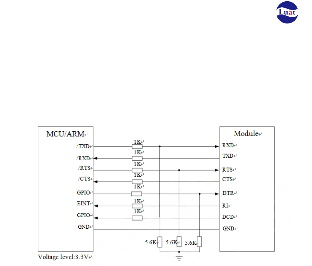
Chart 14:3.3V Level conversion circuit
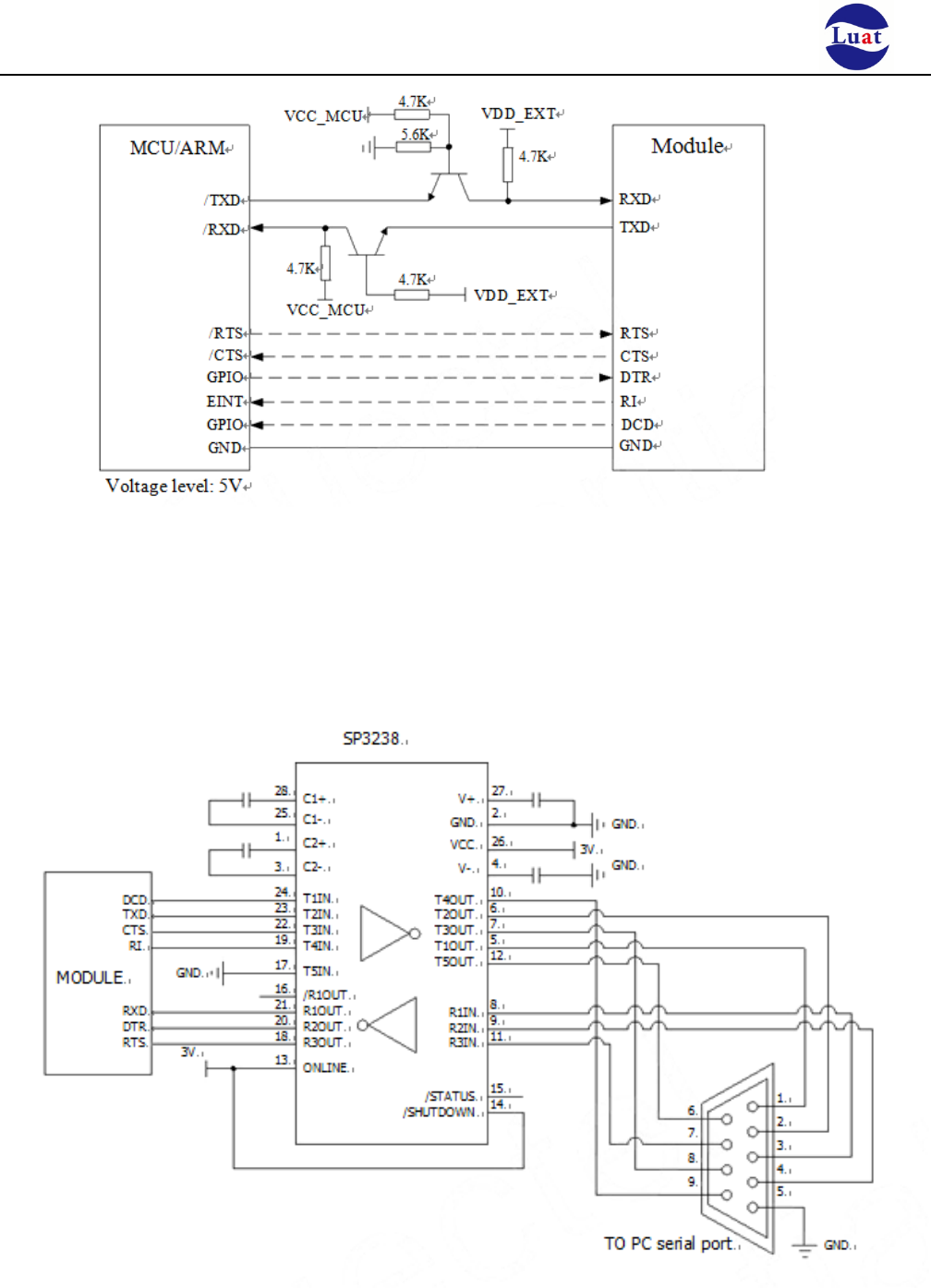
5V system level matching, level matching between the module and peripherals can refer to the following
connections, the dotted line below can refer to the above solid line circuit (the dotted line module to send the
reference module TXD circuit design, the dotted line module Receive reference module RXD circuit design).
VCC_MCU is the client's I / O voltage level. VDDIO is the module output I / O voltage level.
Air208 Hardware Design Manual
Page31 Totally 57 pages
Chart 15:5VLevel conversion circuit
When the module communicates with the PC, you need to add an RS232Level conversion circuit between them.
Because the module's serial port configuration is not RS232 level, only SupportsCMOS level. The following figure
shows the module with PC communication, serial port level conversion circuit.
Chart 16:RS232 Level conversion circuit

noise at DCS1800MHz.
capacitor suppliers, select the most suitable value to filter out work in GSM900MHz, High frequency
Air208 Hardware Design Manual
Page32 Totally 57 pages
4.8. Audio interface
The module provides an analog audio input channel and a channel analog output channel, Supports call,
recording and playback functions。
Table10:Audio interfacePin definition
Interface Interface name Interface no. Function
AIN
MICP 9 Audio input positive end
MICN 10 Audio input negative end
AOUT
SPKP 11 Audio output positive end
SPKN 12 Audio output negative end
AIN can be used as a microphone input or an analog audio signal input. Microphones usually use electret
microphones. AIN1 is a differential input.
AOUT channels can directly drive 8 ohm speakers. The AOUT channel is differential output.
4.8.1. Preventing TDD noise and other noises
As for handheld speakerphone and handsfree microphones It is recommended to use a built‐in RF filter dual
capacitor (such as 10pF and 33pF) electret microphone to filter out radio frequency interference from the
interference source will greatly improve the coupling TDD noise. The 33pF capacitor is used to filter out
high‐frequency interference when the module is operating at 900MHz. If you do not add this capacitor, you may hear
TDD noise during the call. At the same time 10pF capacitor is used to filter out the work in the 1800MHz frequency
high frequency interference. It should be noted that, because the capacitance of the resonance point depends largely
on the material of the capacitor and the manufacturing process, so the choice of capacitor, you need to consult the
The severity of high frequency interference at GSM transmission usually depends mainly on the customer
application design. In some cases, GSM900 TDD noise is more serious, and in some cases, DCS1800 TDD noise is more
serious. Therefore, customers can filter the results of the election according to the needs of the filter capacitor, and
sometimes do not need to paste this type of filter capacitor.
PCB RF filter capacitor placed on the position as close as possible to Audio devices or Audio interface, alignment
as short as possible, to go through the filter capacitor and then to other points.
Position the antenna away from the Audio component and the Audio traces as far as possible to reduce radiated
interference. The Power Supply traces should not be parallel to the Audio traces. The Power Supply traces should be
as far away as possible from the Audio lines.
Differential Audio traces must follow the Layout rules for differential signals.
Air208 Hardware Design Manual
Page33 Totally 57 pages
4.8.2. Microphone interface reference circuit
AIN channel built‐in electret microphone bias voltage. Microphone channel reference circuit shown below:
Chart 17:AIN MICROPHONE CHANNEL INTERFACE CIRCUIT
4.8.3. Audio output interface reference circuit
SPKAudio Output Interface can be directly driven with 8 ohm speaker.
Chart 18:Reference line

Air208 Hardware Design Manual
Page34 Totally 57 pages
4.8.4. Audio Electrical characteristics
Table 11:Typical characteristics of electret microphones
Parameter Minimum Typical Maximum Unit
Working voltage 1.0 1.25 2.0 V
Working current 500 Ma
Impedance 2.2 KΩ
Table 12:Audio interfaceTypical characteristic parameters
Parameter Minimum Typical Maximum Unit
AOUT
Single‐ended
output
Load8Ω
Reference level 02.4Vpp
Differential
output
Load8Ω
Reference level 04.8Vpp
Air208 Hardware Design Manual
Page35 Totally 57 pages
4.9. SIM CARD INTERFACE
The SIM card interface supports the functions of the GSM Phase1 specification, as well as the functions of the
GSM Phase 2+ specification and the FAST64 kbps SIM card (used in the SIM application toolkit).
The SIM card is powered by the internal power supply of the module to support 1.8V and 3.0V power supply.
4.9.1. SIM INTERFACE
The following table describes the SIM interface pin definitions.
Table13:SIM CARD INTERFACEPin definition
Pin name Pin no. Function
SIM_VDD 18 SIM card power supply automatic detects SIM card operating voltage. The
accuracy is 3.0V ± 10% and 1.8V ± 10%. The maximum supply current is
10mA.
SIM_RST 17 SIM card Reset pin
SIM_DATA 15 SIM card data cable
SIM_CLK 16 SIM card clock line
SIM_DET14 SIM card in position detection
The figure below is the reference circuit SIM interface, using of 6pin SIM card connector.
Chart 19:Using a 6pin SIM Card Reference Schematic (SIM)
Air208 Hardware Design Manual
Page36 Totally 57 pages
If you need to use sim card in place detection, the recommended circuit is as follows.
Chart 20:With the detection of PIN SIM card reference circuit diagram
In SIM CARD INTERFACE circuit design, in order to ensure the SIM card's good functional performance and is not
damaged, the circuit design is recommended to follow the following design principles:
♦SIM card holder and the module can not be too far away from the ornaments, the closer the better, try to ensure
that SIM card signal cable is not exceed 20cm.
♦The SIM card signal cable is routed away from the RF cable and the VBAT power cable.
♦The wiring width of SIM_VDD is not less than 0.3mm and the bypass circuit between SIM_VDD and SIM_GND
should not exceed 1uF and be placed close to the SIM card holder.
♦In order to prevent possible SIM_CLK signal crosstalk on the SIM_DATA signal, the two wiring should not be too
close, increase the shielding between the two traces. And SIM_RST signal also needs protection.
♦In order to ensure good ESD protection, it is recommended to add TVS tube, and placed near SIMcassette. The
selected ESD device has a parasitic capacitance of no more than 50pF, such as WILL (http://www.willsemi.com)
ESDA6V8AV6. A 22 ohm resistor can be connected in series between the module and the SIM card to suppress
stray EMI and enhance ESD protection. The SIM card's peripheral circuitry must be as close as possible to
SIMcassette.
4.9.2. 6-pin SIM card holder
Using a 6‐pin SIM card holder, Amphenol's C70710M0065122 is recommended. Visit http://www.amphenol.com
for more information.
Air208 Hardware Design Manual
Page37 Totally 57 pages
Chart 21:Amphenol C707 10M006 512 2 SIM cassette
Air208 Hardware Design Manual
Page38 Totally 57 pages
4.10. RI SIGNAL ACTION
Table 14:RI SIGNAL ACTION
Status RI response
StandbyHigh level
Voice call After switching to low level:
(1)When the call is switched on to a high level
(2)Use the AT command ATH hang up the voice, RI goes high
(3)The caller hangs up, RI first goes high, then pulls low for 120ms, receives an auto‐reply URC message
"NO CARRIER" and then goes high
(4)When SMS is received, it becomes high level
Data
transmission
After switching to low level:
(1)It changes to high level when data connection is set up.
(2)Use the AT command ATH to suspend data connections, and RI to a high level
(3)The caller hangs up, RI first into high level, then pull to a low level for 120ms, received automatic
reply message "NO URC CARRIER", and then into high level
(4)When SMS is received, it becomes high level
SMS When a new message is received, RI goes low for 120ms and then goes high.
URC Some URC information can trigger RI to pull low 120ms
If the module is used as a calling party, the RI remains high except when receiving URC messages or text
messages. When the module is used as the called party, the timing of RI is as follows:
Chart 22:The module is used as called party RI timing for voice call
Air208 Hardware Design Manual
Page39 Totally 57 pages
Chart 23:The module is used as called party RI timing for data call
Chart 24:RI timing of module calling
Chart 25:RI timing when receiving URC message or SMS
Air208 Hardware Design Manual
Page40 Totally 57 pages
4.11. Network status indication
NET_LEDpin signal can be used to indicate the status of the network lights. The working status of this pin is shown in
the following table:
Table 15:NET_LED working status
Status Module function
Shutdown The module is not running
Bright 64ms,off 800ms Can not find the network
Bright 64ms,off 3000ms Registered on network
Bright 64ms,off 300ms GPRS cimmunication
not registered on the GSM network:
Chart 26:NETLIGHTReference circuit
Air208 Hardware Design Manual
Page41 Totally 57 pages
4.12. PWM
Air208supports 2 PWM outputs: PWM, LPG, multiplexed by UART2_RX and UART2_TXD respectivel.
UART2
Pin name Pin no. I/O Pin description Electrical characteristics Remark
UART2_RXD
(LPG) 23 I
Hardware UART2
VILmin=-0.3V
VILmax=0.25×VDDIO
VIHmin=0.75×VDDIO
VIHmax=VDDIO+0.3
VOHmin=0.85×VDDIO
VOLmax=0.15×VDDIO
Hang when not in
usage
UART2_TXD
(PWM) 22 O
LPG (Light Pulse Generation) For low frequency applications such as driving LED flashes, only a fixed seven
kinds of cycle (Unitms) can be set: 125,250,500,1000,1500,2000,2500,3000. And 15 kinds of high time.
PWM, frequency range (80‐65535HZ), and various duty cycles can be set.
Please refer to the corresponding AT command document.
5. Radio interface
pin 32 is the RF antenna input. RFInterface50 ohm impedance matching.
Table 16:RF_ANTPin definition
Pin namePin no. Function
RF_ANT 32RF pad
Air208 Hardware Design Manual
Page42 Totally 57 pages
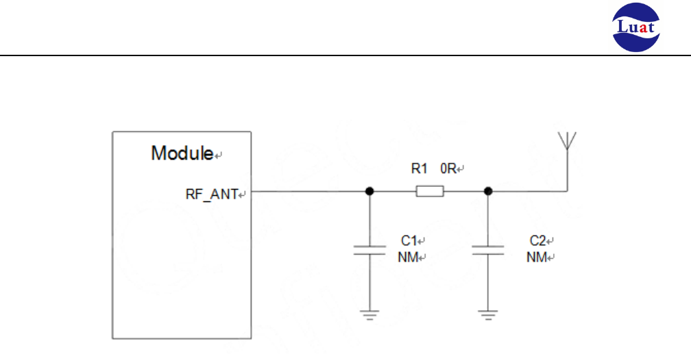
5.1. RF reference circuit
Chart 27:RF reference circuit
Air208 pads must be microstrip or other types of RF traces and the impedance must be controlled to about 50
ohms. For better RF performance, ground pads are on each side o
f
the RF input port.
Care must be taken to minimize the losses on the RF traces or RF cables. The recommended insertion loss must
meet the following conditions:
♦EGSM850<1dB
♦DCS1900<1.5dB
Air208 also built an RF connector to facilitate users to directly connect the module RF coaxial antenna, and save
the board on the RF routing:
Air208 Hardware Design Manual
Page43 Totally 57 pages

Air208 Hardware Design Manual
Page44 Totally 57 pages
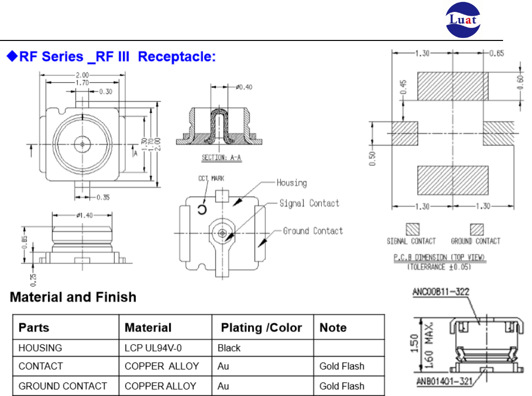
Corresponding coaxial connector as shown below:
5.2. RF CONDUCTION SENSITIVITY
Table 18:RF CONDUCTION SENSITIVITY
Band Receiving sensitivity
EGSM850
DCS1900
< -108.5dBm
< -108.5dBm
Air208 Hardware Design Manual
Page45 Totally 57 pages
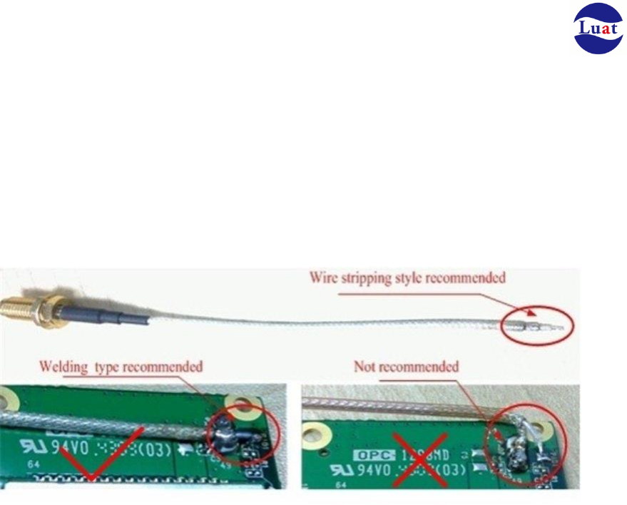
5.3. Recommended RF welding method
If the RF connector for connecting the external antenna is connected to the module by soldering, be sure to
pay attention to the stripping method and soldering method of the connecting wire. In particular, if the soldering is
sufficient, follow the correct soldering method shown in the figure below, In order to avoid due to poor welding
caused by line loss increases.
Chart 28:Suggestion on RF welding method

Air208 Hardware Design Manual
Page46 Totally 57 pages
6. Electrical characteristics, reliability, RF characteristics
6.1. Absolute Maximum
The following table shows the module digital, analog pin Power Supply supply voltage and current Maximum
tolerance value.
Table20:Absolute Maximum
Parameter Minimum Maximum Unit
VBAT ‐0.3 4.2 V
Power supply peak current 0 2 A
Power supply average current (TDMA one
frame time)
00.7A
Digital pin voltage ‐0.3 3.3 V
Analog pin voltage ‐0.3 3.0 V
Off / Off mode digital / analog pin voltage ‐0.25 0.25 V
6.2. working temperature
Table 21:working temperature
Temperature Minimum Typical Maximum Unit
Nornal working
temperature
‐40 25 85 ℃
storagetemperature ‐45 90 ℃

Air208 Hardware Design Manual
Page47 Totally 57 pages
6.3. Voltage limit value
Table 22:Module power limit value
ParametDescription Condition Minimum Typical Maximum Unit
VBAT
Supply voltage
The voltage must be within this range,
including voltage drops, ripple, and
spikes
3.4 3.8 4.2V
Burst voltage
drop at launch
GSM900 MaximumTransmit
power level
400 mV
IVBAT
Average
supply
current
Shutdown
mode
Power on for the
first time 34 uA
Shutdown after
boot(RTC works
normally)
101 uA
Bottom current 0.8 mA
Standby current
DRX=2 1.4 mA
DRX=5 1.14 mA
DRX=9 1.03 mA
Flight Mode AT+CFUN=4 0.896 mA
Minimum function mode
AT+CFUN=0
0.763 mA
GPRS mode
(2 send,2
receive)
EGSM 900 1) 315.9 mA
DCS1800 2) 208.7 mA
GPRS mose
(4 receive,1
send)
EGSM 900 1) 203.5 mA
DCS1800 2) 150.1 mA
Peak current
/ GSM900 transmit
GSM900 MaximumTransmit
power level
1.8 2 A

Air208 Hardware Design Manual
Page48 Totally 57 pages
time slot)
1) 1) power level 52)power level 0

Air208 Hardware Design Manual
Page49 Totally 57 pages
6.4. Current consumption
Table 23:Module's current consumption
Condition Current consumption
GPRS data transmission
Data transmission mode, GPRS ( 2 receive, 2 send) CLASS8 & CLASS 12
EGSM850 @Power level5,<550mA,Typicalvalue 315.9mA
@Power level10,Typicalvalue 158.2mA
@Power level19,Typicalvalue 83.5mA
DCS1900 @Power level0,<450mA,Typicalvalue208.7mA
@Power level5,Typicalvalue125mA
@Power level15,Typicalvalue78.4mA
Data transfer mode, GPRS ( 4 receive, 1send) CLASS8 & CLASS 12
EGSM850
@Power level5,<350mA,Typicalvalue203.5mA
@Power level10,Typicalvalue101.3mA
@Power level19,Typicalvalue62.4mA
DCS1900 @Power level0,<300mA,Typicalvalue150.1mA
@Power level5,Typicalvalue79.4mA
@Power level15,Typicalvalue55.8mA

Air208 Hardware Design Manual
Page50 Totally 57 pages
6.5. Static Protection
In the module application, due to the human body static electricity, static electricity generated between the
microelectronic electrostatic friction, through various means of discharge to the module, may cause some damage to
the module, so ESD protection must pay attention to, whether in the production assembly, testing , R & D process,
especially in product design, should take ESD protectionmeasures.ForexampleESDprotectionshouldbeaddedin
circuit design at the Interface or vulnerable to ESD point. To wear anti‐ESD gloves in production and so on.
The following table shows the ESD withstand voltage of the module PIN pin.
Table 24:ESDP erformance parameters (temperature: 25 C, humidity: 45%))
Pin name Contact discharge Air discharge
VBAT,GND ±5KV ±10KV
RF_ANT ±5KV ±10KV
TXD, RXD ±2KV ±4KV
Others ±0.5KV ±1KV

Air208 Hardware Design Manual
Page51 Totally 57 pages
7. phycial dimension
This section describes the module's phycial dimension and the recommended package dimensions for the
customer's design using the module.
Air208 Hardware Design Manual
Page52 Totally 57 pages
7.1. Module phycial dimension
Chart 29:Air208 Front view (unit: mm)
Air208 Hardware Design Manual
Page53 Totally 57 pages
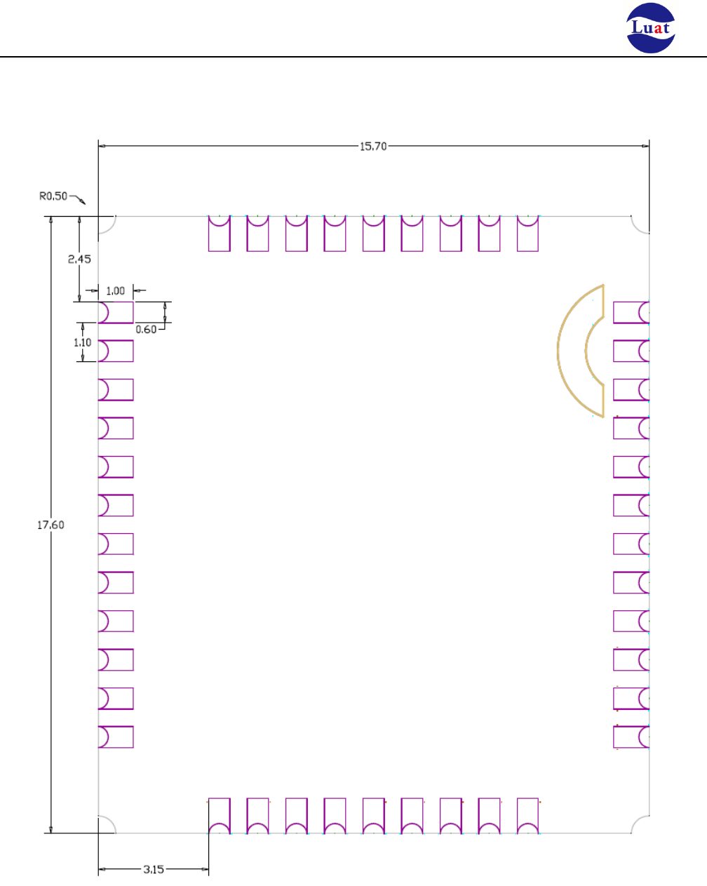
7.2. Recommended PCB encapsulation
Chart 30:Recommended encapsulation (Unit: mm)
Note: make sure the spacing between module on the PCB and other components is 3mm at least.
Air208 Hardware Design Manual
Page54 Totally 57 pages
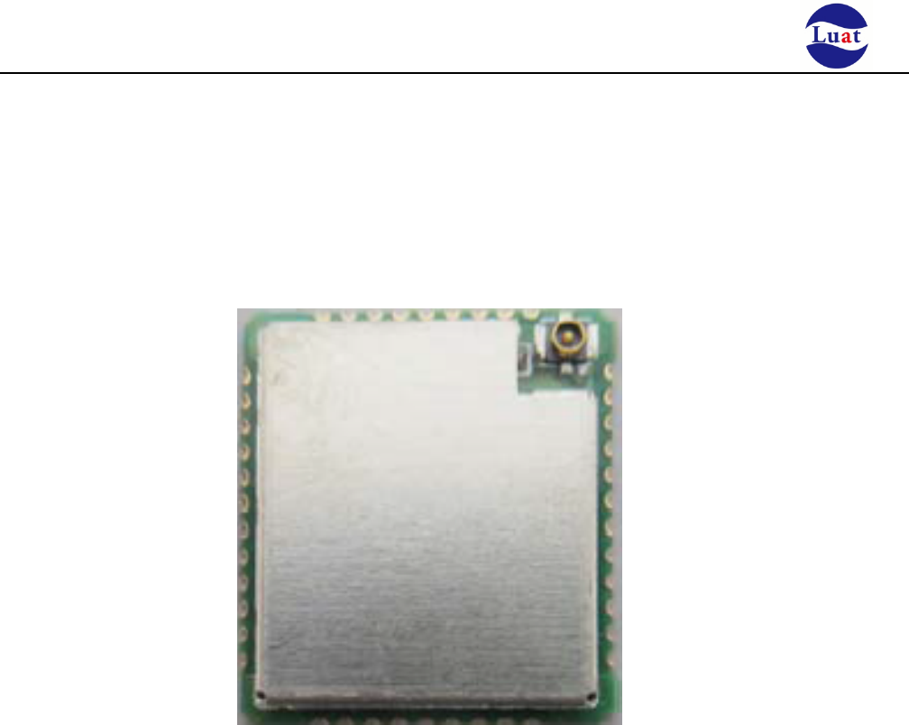
7.3. Module front view
Chart 31:Module front view
Air208 Hardware Design Manual
Page55 Totally 57 pages
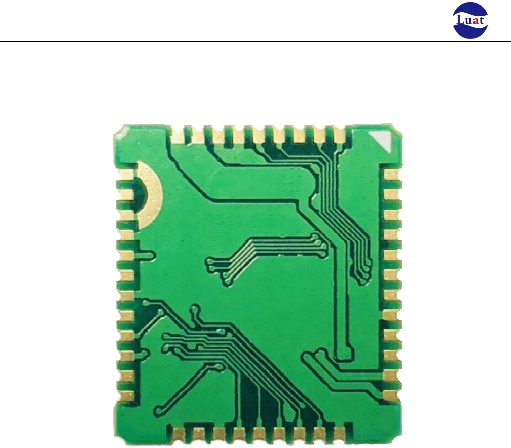
7.4. Module bottom view
Chart 32:Module bottom view
8. Storage and production
8.1. Storage
Air208shipped in vacuum sealed bags. The storage of the module needs to follow the following conditions:
The module can be stored in a vacuum‐sealed bag for 12 months at ambient temperatures below 40 ° C and air
humidity less than 90%.
When the vacuum sealed bags open, if the following conditions are met, the module can be directly reflow or other
high‐temperature processes:
♦Module ambient temperature below 30 degrees Celsius, air humidity less than 60%, the factory completed patch
within 72 hours.
Air humidity is less than 10%.
Air208 Hardware Design Manual
Page56 Totally 57 pages
If the module is in the following conditions, it is necessary to bake before the patch:
♦When the ambient temperature is 23 degrees Celsius (5 degrees Celsius allowed fluctuations), the humidity
indicator shows humidity greater than 10%
♦When the vacuum sealed bag is opened, the module ambient temperature is below 30 degrees Celsius and the
air humidity is less than 60%, but the factory failed to complete the patch within 72 hours
When the vacuum sealed bag is opened, the module storage air humidity is greater than 10%.
If the module needs to be baked, please bake for 48 hours at 125 degrees Celsius (allowing 5 degrees Celsius
fluctuation).
Note: The module packaging can not withstand such a high temperature, remove the module package before the
module is baked. If you only need a short baking time, please refer to the IPC / JEDECJ‐STD‐033 specification.
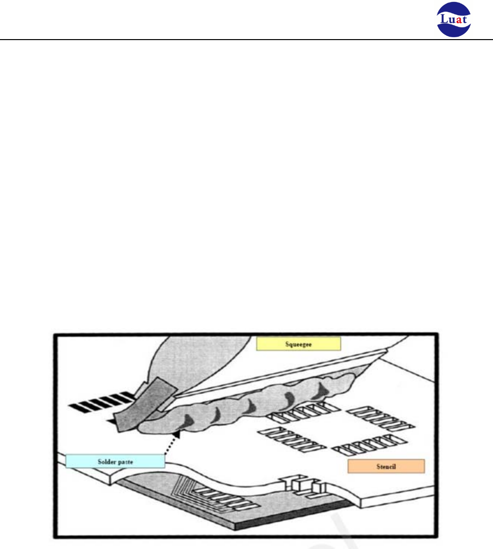
8.2. Production welding
Printed scraper on the screen printing solder paste, solder paste through the screen openings to the PCB on the
leakage, printing scraper strength needs to be adjusted properly, in order to ensure the quality of module paste,
Air202 module pad part of the corresponding stencil thickness should be 0.2mm.
Chart 33:Paste map
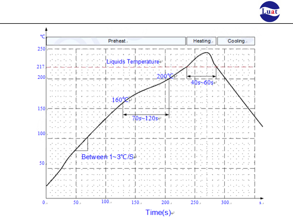
To avoid repeated heating damage to the module, it is recommended that the customer PCB board be reflowed
after the first side o
f
the module. The recommended Furnace temperature curve is shown below:
Air208 Hardware Design Manual
Page57 Totally 57 pages
Chart 34:Furnace temperature curve
FCC Statement
Any Changes or modifications not expressly approved by the party responsible for
compliance could void the user’s authority to operate the equipment.
This device complies with part 15 of the FCC Rules. Operation is subject to the
following two conditions:
(1) This device may not cause harmful interference, and
(2) This device must accept any interference received, including interference that may
cause undesired operation.
FCC Radiation Exposure Statement:
This equipment complies with FCC radiation exposure limits set forth for an
uncontrolled environment .This equipment should be installed and operated with
minimum distance 20cm between the radiator& your body.
FCC Label Instructions
The outside of final products that contains this module device must display a label referring to the
enclosed module. This exterior label can use wording such as: "Contains Transmitter Module FCC
ID: 2AEGG-AIR208 or “Contains FCC ID:2AEGG-AIR208 , Any similar wording that expresses
the same meaning may be used.