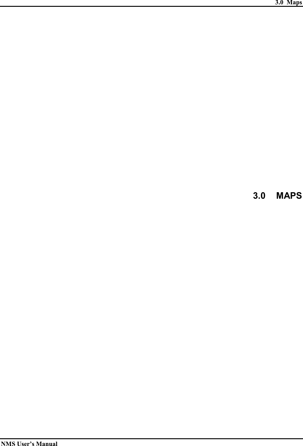
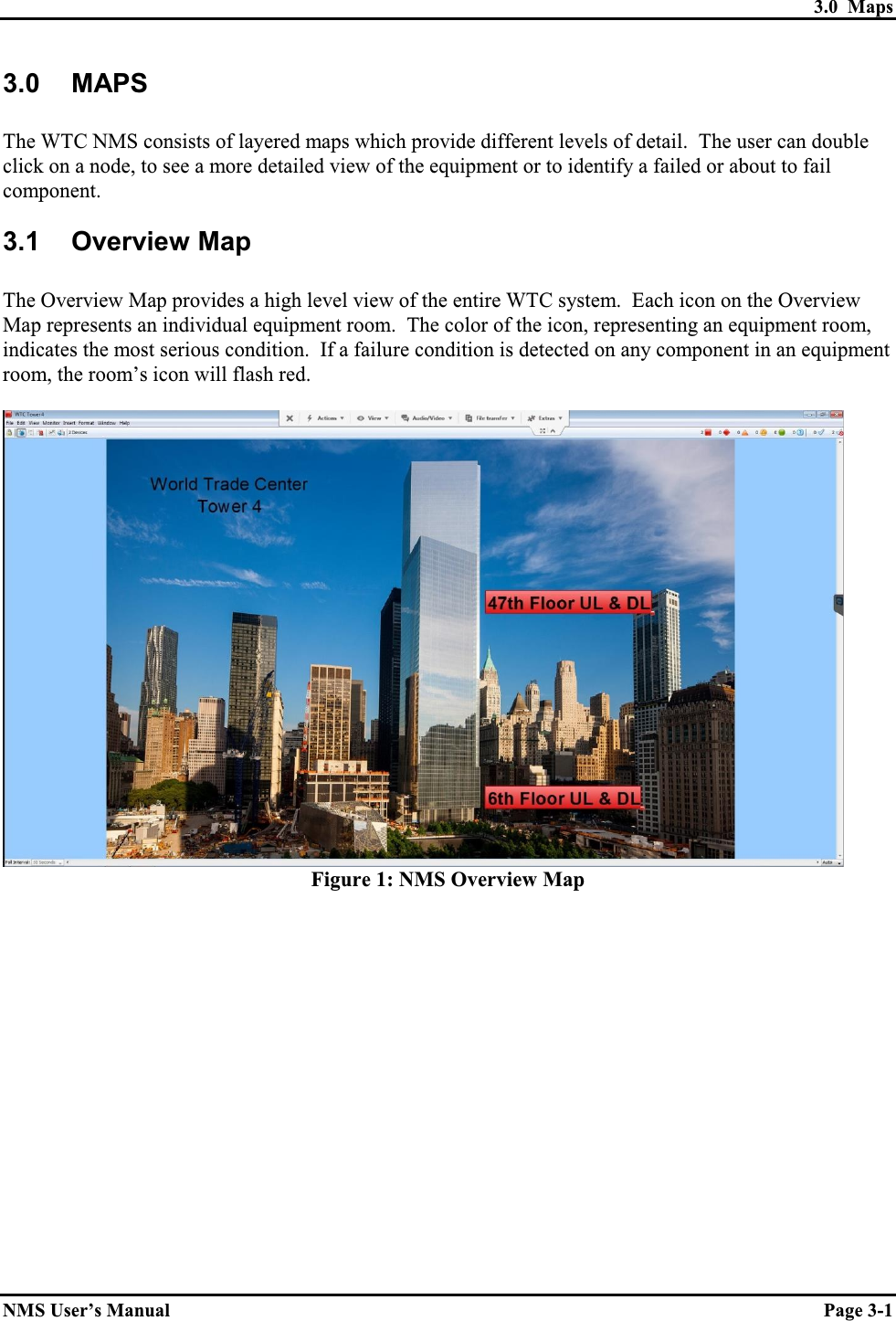
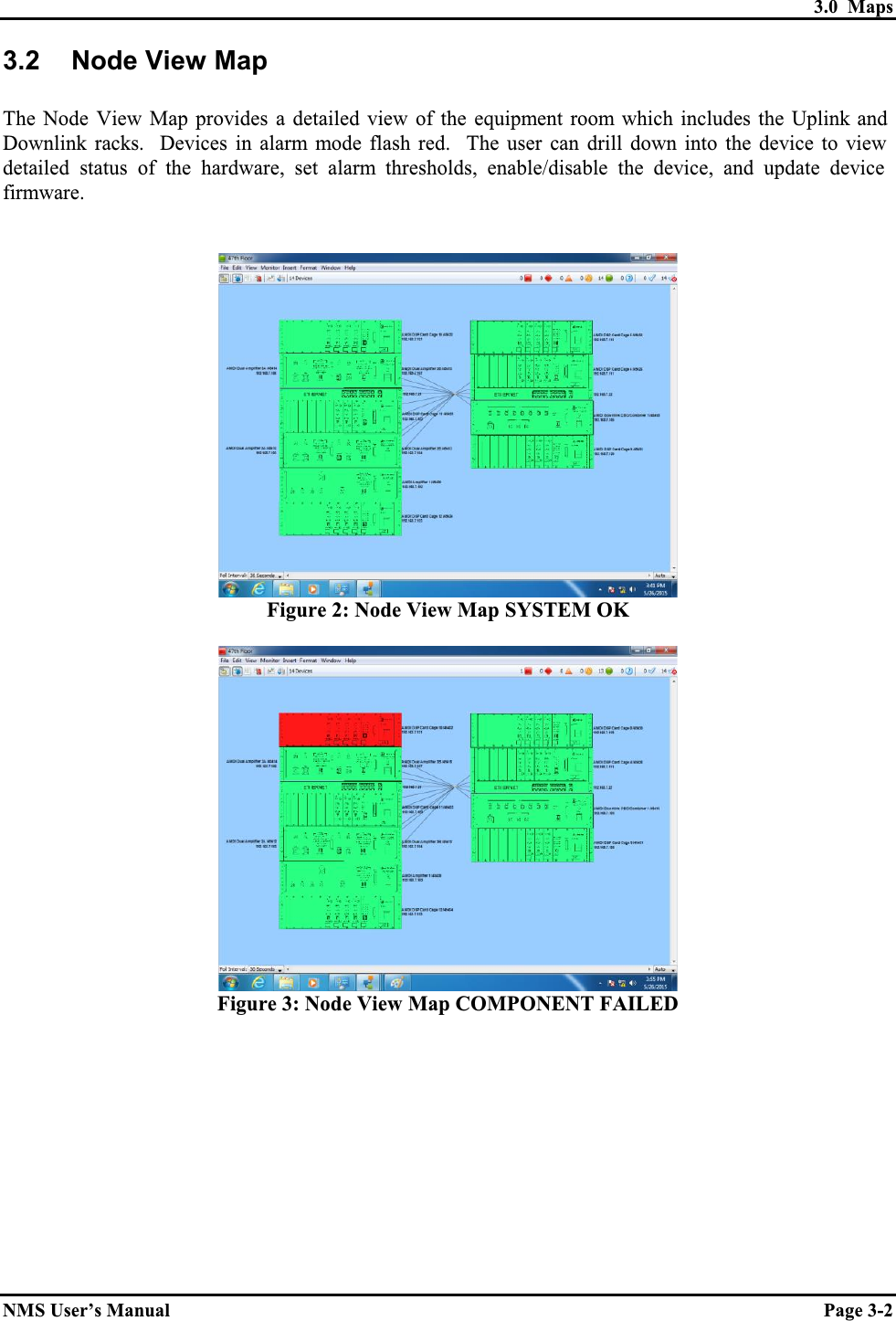
Applied Micro Design 1465 Model 1465 UHF Multi-Carrier In-Building Amplifier User Manual Rev 6
Applied Micro Design, Inc Model 1465 UHF Multi-Carrier In-Building Amplifier Users Manual Rev 6
UserManual.wiki
>
Applied Micro Design
>
1465 User Manual
Users Manual Rev 6
Navigation menu
Upload a User Manual
Namespaces
Wiki Guide
HTML
PDF
Info
Views
User Manual
Discussion / Help
Navigation

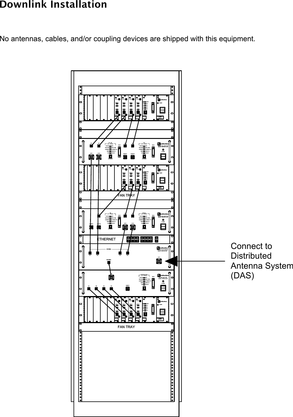
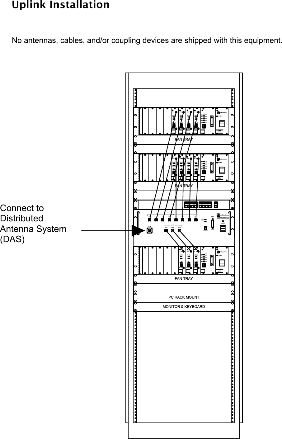
![Part 90 (Class B) Signal BoostersWARNING. This is NOT a CONSUMER device. It is designed for installation by FCC LICENSEES and QUALIFIED INSTALLERS. You MUST have an FCC LICENSE or express consent of an FCC Licensee to operate this device. You MUST register Class B signal boosters (as defined in 47 CFR 90.219) online at www.fcc.gov/signal-booster/registration. Unauthorized use may result in significant forfeiture penalties, including penalties in excess of $100,000 for each continuing violation. This is a Class B Booster.Notes, Cautions, and Warnings!Connect RF Output to existing Distributed Antenna System (DAS) cable only. DO NOT operate equipment with unauthorized antennas, cables, and/or coupling devices. DO NOT operate equipment unless all RF connectors are secure. DO NOT operate equipment unless it has been installed and inspected by a qualified radio technician. Contact Information For more information contact the FCC at: https://signalboosters.fcc.gov/signal-boosters/F.2 PART 90 CLASS B SIGNAL BOOSTERS Licensees and signal booster operators are required to register existing Class B signal booster installations with the FCC by November 1, 2014. After November 1, 2014, operation of an existing, unregistered Class B signal booster will be unauthorized and subject to enforcement action. Any new Class B signal booster installed after November 1, 2014 must be registered prior to operation. To encourage compliance with this new requirement, registration will be free of cost to the operator and/or licensee.[R11], [R9] FCC Part 90 Class B Signal Booster Registration & Discovery website: https://signalboosters.fcc.gov/signal-boosters/](https://usermanual.wiki/Applied-Micro-Design/1465/User-Guide-2725421-Page-3.png)