Applied Micro Design 1465 Model 1465 UHF Multi-Carrier In-Building Amplifier User Manual Rev 6
Applied Micro Design, Inc Model 1465 UHF Multi-Carrier In-Building Amplifier Users Manual Rev 6
Users Manual Rev 6

WTC4
Head End System
Channelized Bi-Directional Amplifier
User’s Manual
rev 6
19516 Amaranth Drive Germantown MD 20874 ph 301.540.9506 | info@appliedmicrodesign.com | www.appliedmicrodesign.com
Applied Micro Design Inc.

Table of Contents
Notes, Cautions, and Warnings
System Description
System Block Diagram
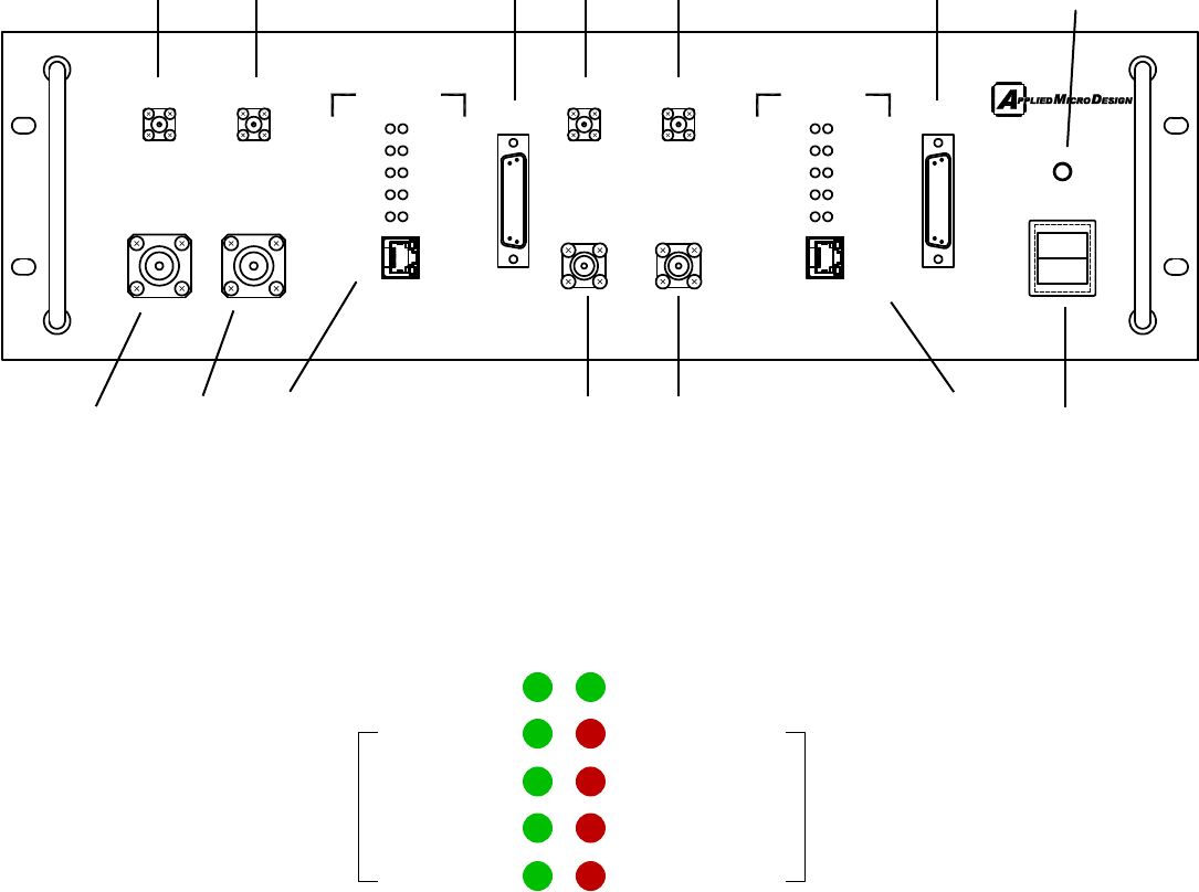
Downlink Rack
Uplink Rack
DSP Card Cage
DSP Front Panels & Indicators
DSP Description & Specifications
Dual Power Amplifier Front Panel & Indicators
Single Power Amplifier Front Panel & Indicators
Power Amplifier Description & Specifications
CBC/Combiner Front Panel
CBC/Combiner Description & Specifications
CBC/Splitter Front Panel & Indicators
CBC/Splitter Description & Specifications
Downlink Rack RF Cable Interconnection
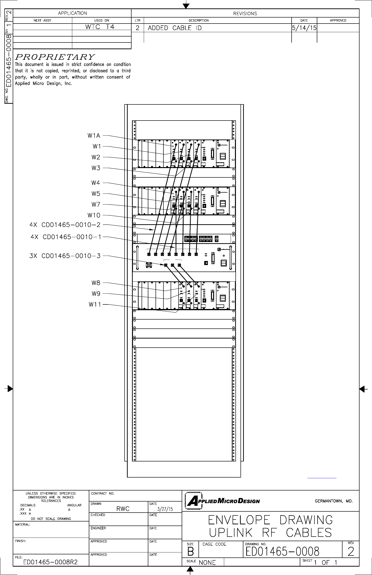
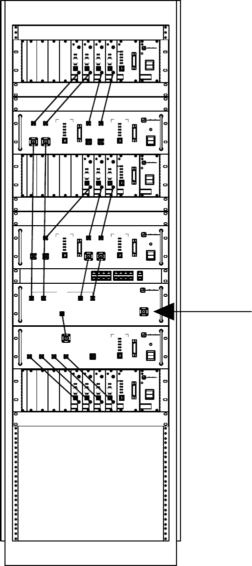
Uplink Rack RF Cable Interconnection
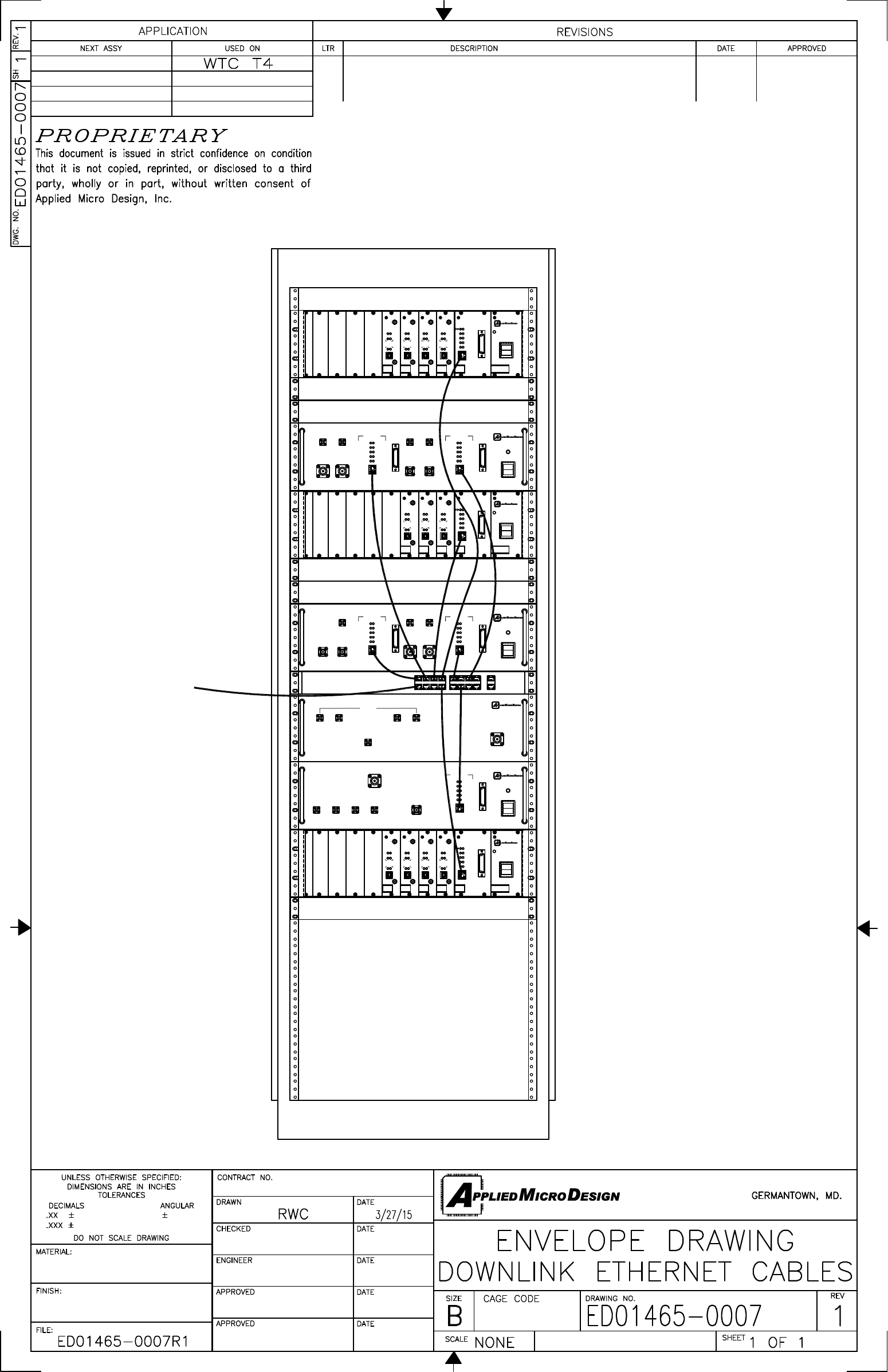
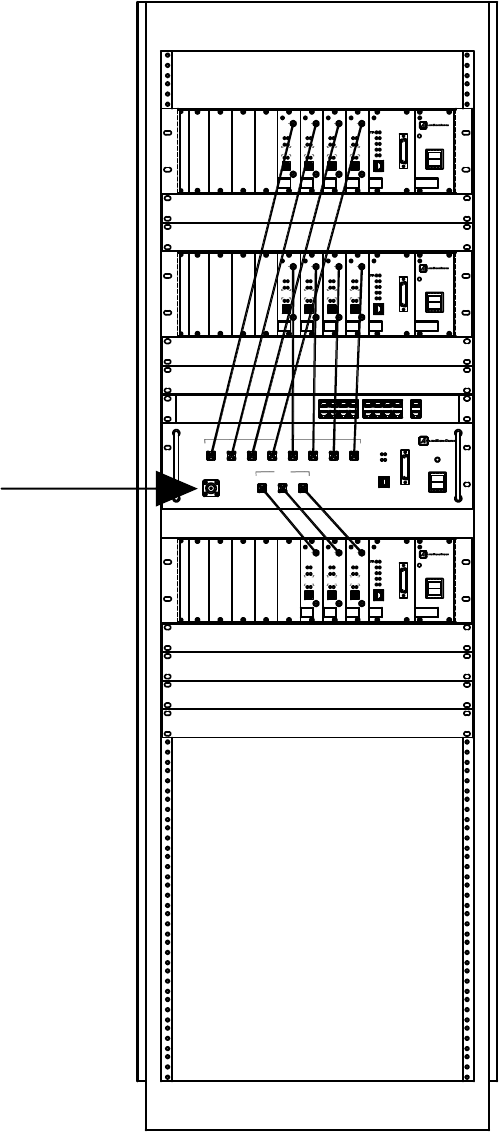
Downlink Rack Ethernet Cable Interconnection
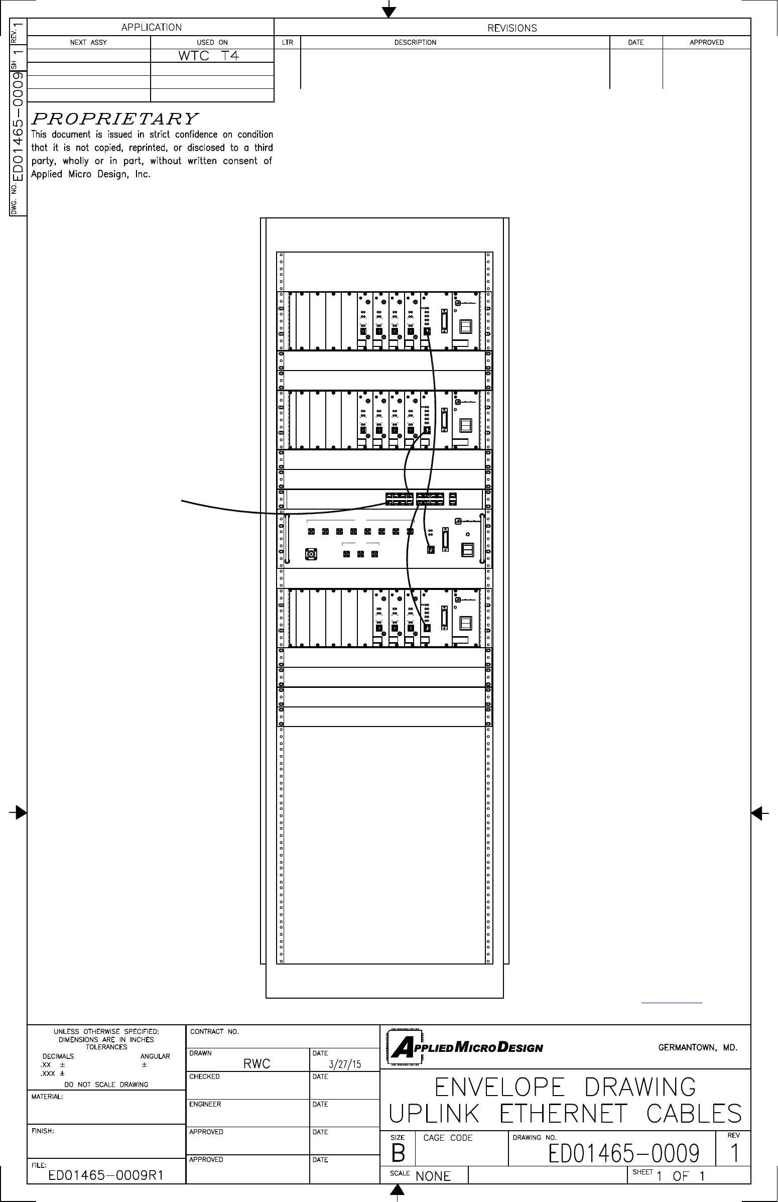
Uplink Rack Ethernet Cable Interconnection
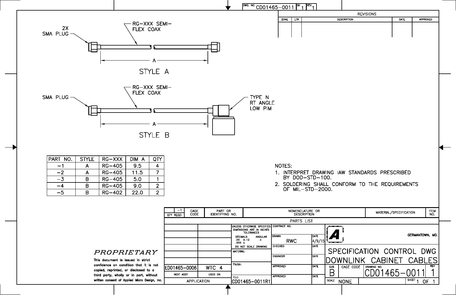
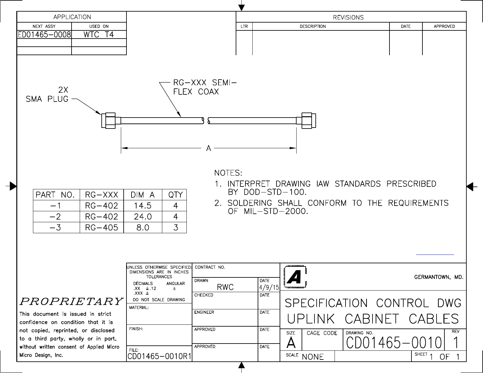
Downlink Cabinet RF Cables
Uplink Cabinet RF Cables
Downlink Installation
Uplink Installation
Appendix A - NMS GUI Manual
Appendix B - RACS (Radio Access Control System) Description
Appendix C - DSP User GUI Operation

Part 90 (Class B) Signal Boosters
WARNING. This is NOT a CONSUMER device. It is designed for installation by FCC
LICENSEES and QUALIFIED INSTALLERS. You MUST have an FCC LICENSE or express
consent of an FCC Licensee to operate this device. You MUST register Class B signal
boosters (as defined in 47 CFR 90.219) online at www.fcc.gov/signal-booster/registration.
Unauthorized use may result in significant forfeiture penalties, including penalties in excess of
$100,000 for each continuing violation.
This is a Class B Booster.
Notes, Cautions, and Warnings
!Connect RF Output to existing Distributed Antenna System (DAS) cable only.
DO NOT operate equipment with unauthorized antennas, cables, and/or coupling
devices.
DO NOT operate equipment unless all RF connectors are secure.
DO NOT operate equipment unless it has been installed and inspected by a qualified
radio technician.
Contact Information
For more information contact the FCC at:
https://signalboosters.fcc.gov/signal-boosters/
F.2 PART 90 CLASS B SIGNAL BOOSTERS Licensees and signal booster operators are
required to register existing Class B signal booster installations with the FCC by November
1, 2014. After November 1, 2014, operation of an existing, unregistered Class B signal
booster will be unauthorized and subject to enforcement action. Any new Class B signal
booster installed after November 1, 2014 must be registered prior to operation. To
encourage compliance with this new requirement, registration will be free of cost to the
operator and/or licensee.[R11], [R9]
FCC Part 90 Class B Signal Booster Registration & Discovery website:
https://signalboosters.fcc.gov/signal-boosters/
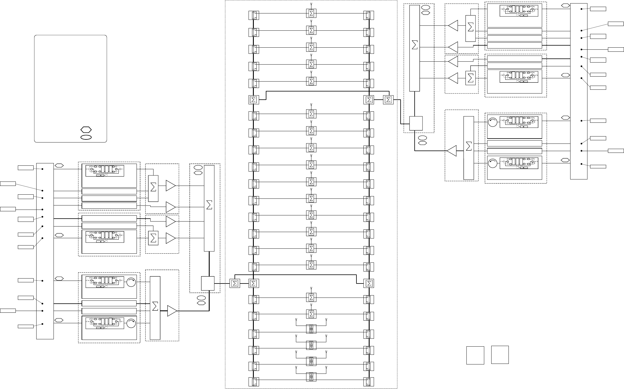
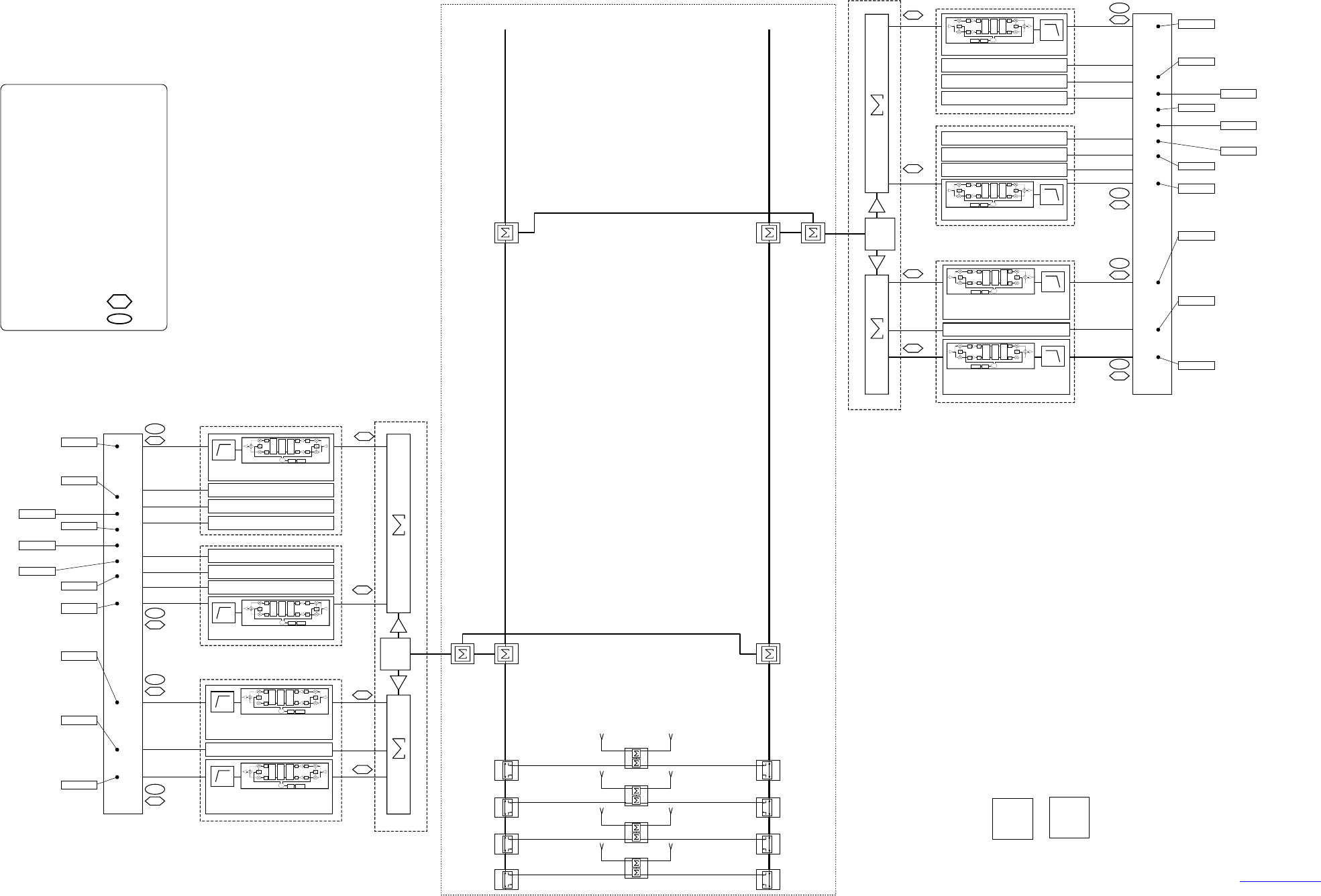
Introduction
There are three major components to the Tower-4 system; the Head-End hardware, the Distributed Antenna System
(DAS) hardware, and the Site-Wide Network (SWN).
Signals from the SWN are input to the Downlink (DL) Head-End (HE) hardware. These signals are filtered and amplified
by the HE DL, and fed into the DAS.
Signals from the DAS are input to the Uplink (UL) HE hardware. These signals are filtered and amplified by the HE UL,
and fed into the SWN.
There are two equipment rooms in Tower-4, and each equipment room has an Uplink and Downlink rack. One each of
these racks (one UL and one DL) will be tested.
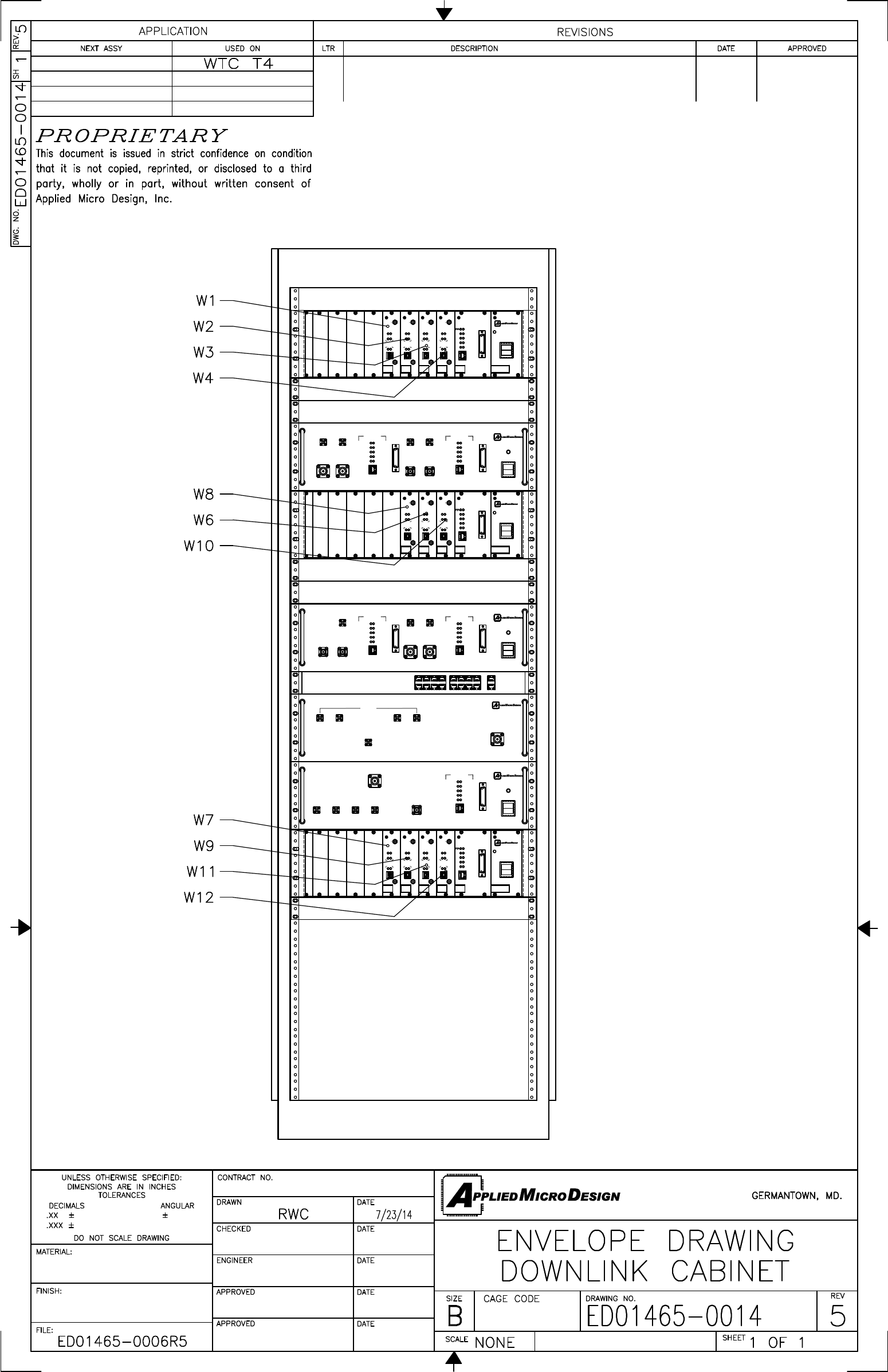
The Downlink Rack contains three DSP Card Cages, two Dual Amplifiers, one Single Amplifier, and one CBC chassis. The
signals are combined in the CBC chassis and fed to the DAS.
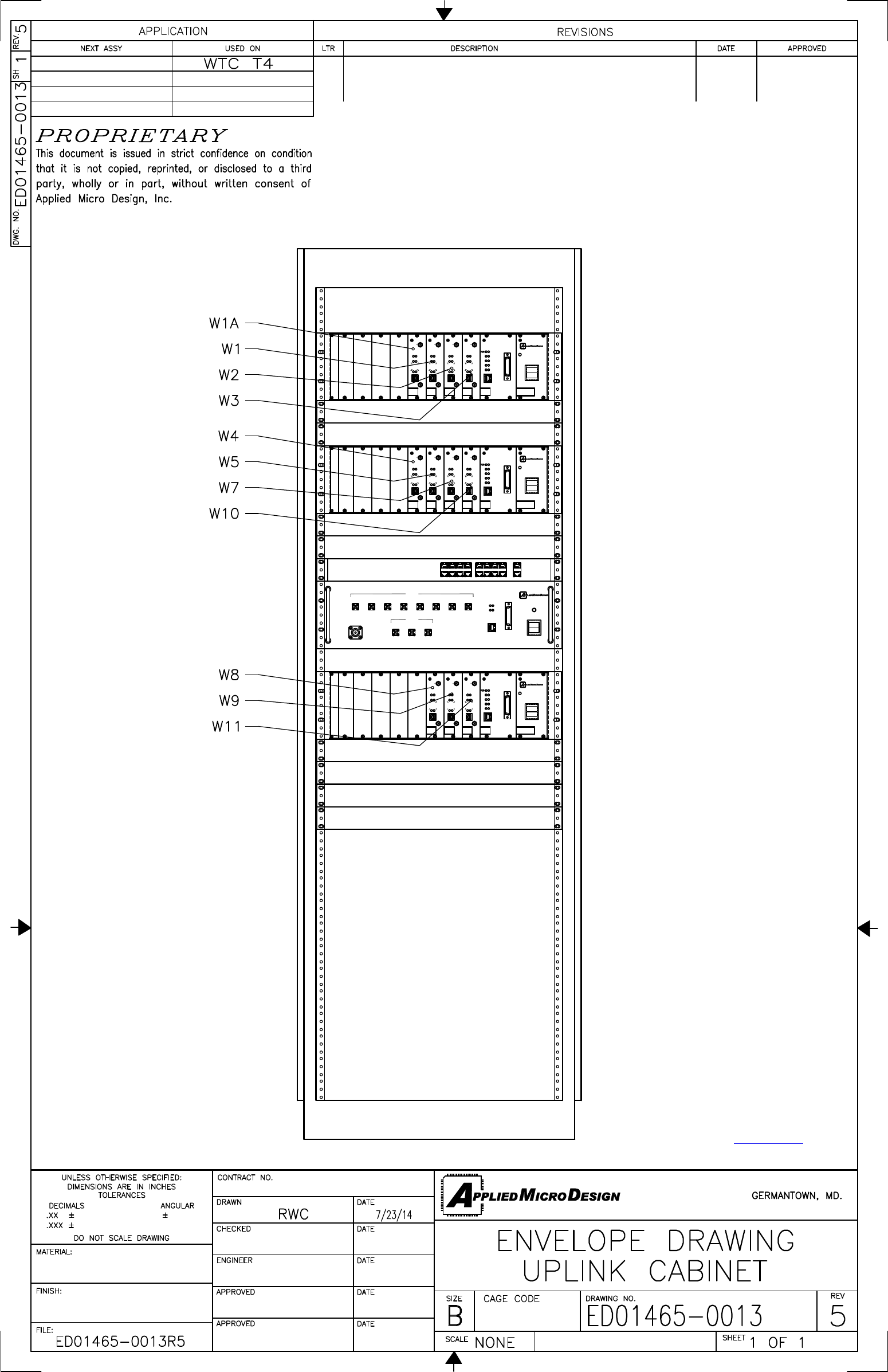
The Uplink Rack contains three DSP Card Cages and one CBC chassis. Signals from the DAS are input to the CBC
chassis.
The UL and DL Channel Cards are the same design. They are FPGA-based designs, programmed essentially as active
digital filters. The cards have a standard line-up; Analog-to-Digital Conversion, Digital Demodulation to baseband, digital
filtering in the FPGA, Digital Modulation back to the original carrier frequency, and Digital-to-Analog conversion. The DSP
Channel Cards can be programmed for multiple filters to process multi-carrier signals.
Head-End Downlink Group
There are eleven SWN windows (seven 400 MHz and four 800 MHz) input to the HE channel cards. Each window is input
to a separate card; each card is set for one wide-band filter to pass multi-carrier signals, and is set for a specified gain.
Wide-band filters for the DL are specified to achieve the required Group or Propagation Delay of 10 μs.
The Site Wide Network (SDN Demarc) provides a constant level of -10 dBm per carrier into each Downlink Channel Card.
The outputs of the Downlink Channel Cards are input to power amplifiers, either directly or via a combiner. Window
groupings to the power amplifiers are shown on the system block diagrams.
The gain of the Downlink Channel Cards are set to have an output of +20 dBm per carrier (100 mW) at the output of the
power amplifiers, with -10 dBm per carrier at the input of the Downlink Channel Cards. The 800 MHz Downlink Channel
Cards are set to have an output of +22 dBm at the output of the power amplifiers.
The power amplifiers are very linear and can handle multiple carriers. The ALC (Automatic Level Control) of each amplifier
is set to provide a maximum of +37 dBm (5W).
The outputs of the 400 MHz and 800 MHz power amplifiers are combined through combiners and low-loss CBC (Cross-
Band Couplers). The output of the CBC is the connection into the DAS.
Head-End Uplink Group
There are eleven windows (seven 400 MHz and four 800 MHz) input to the UL channel cards from the DAS. Each window
is input to a separate card; each card is set for one or more narrow-band filter to pass multi-carrier signals. Narrow-band
filters for the UL are specified to achieve the required Group or Propagation Delay of 25 μs.
A group of frequencies (window grouping) is assigned to one Uplink Channel Card. The signals coming from the DAS are
amplified with an LNA (low-noise amplifier) and distributed to the Uplink Channel Cards using a CBC and splitters.
The Uplink Channel Cards will receive multi-carrier signals in the range of -83 dBm to -33 dBm per carrier. Each Uplink
Channel Card uses AGC (Automatic Gain Control) to maintain an output level of -33 dBm. The Site Wide Network or SDN
Demarc requires no more than -33 dBm per carrier.
PROPRIETARY
This document is issued in strict confidence on condition that it is
not copied, reprinted, or disclosed to a third party, wholly or in part,
without written consent of Applied Micro Design, Incorporated.
WTC4 System Block Diagram
rev 9
B1
2nd
Downlink Group
DAS
UPS
DC
Bias
A B
S3DL02
J1
J2
J3
J1
J2
J3
J1 J2
J3 J4
J1
J2
J3
J1
J2
J3
J1 J2
J3 J4
J1
J2
J3
J1
J2
J3
J1 J2
J3 J4
J1
J2
J3
J1
J2
J3
J1
J2
J3
J1
J2
J3
J1 J2
J3 J4
J1
J2
J3
J1
J2
J3
J1
J2
J3
J1
J2
J3
J1
J2
J3
J1
J2
J3
J1
J2
J3
J1
J2
J3
J1
J2
J3
J1
J2
J3
J1
J2
J3
J1
J2
J3
J1
J2
J3
J1
J2
J3
J1
J2
J3
J1
J2
J3
J1
J2
J3
J1
J2
J3
J1
J2
J3
J1
J2
J3
J1
J2
J3
J1
J2
J3
J1
J2
J3
J1
J2
J3
J1
J2
J3
J1
J2
J3
J1
J2
J3
J1
J2
J3
J1
J2
J3
J1
J2
J3
J1
J2
J3
J1
J2
J3
B2
B3
B4
5th
10th
14th
18th
22nd
26th
30th
34th
38th
42nd
46th
50th
54th
58th
62nd
65th
6th
47th
S3DL05
S3DL10
S3DL14
S3DL18
S3DL22
S3DL26
S3DL30
S3DL34
S3DL38
S3DL42
S3DL46
S3DL50
S3DL54
S3DL58
S3DL62
S3DL65
S4DLB1
S4DLB2
S4DLB3
S4DLB4
S1DL47
S2DL47S2DL47
S1DL06
S2DL06 S2DL06
T1DLB4A
T1DLB3A
T1DLB2A
T1DLB1A
T1DL02A
T1DL05A
B1
2nd
B2
B3
B4
5th
10th
14th
18th
22nd
26th
30th
34th
38th
42nd
46th
50th
54th
58th
62nd
65th
T1DL10A
T1DL14A
T1DL18A
T1DL22A
T1DL26A
T1DL30A
T1DL34A
T1DL38A
T1DL42A
T1DL46A
T1DL50A
T1DL54A
T1DL58A
T1DL62A
T1DL65A
T1DL50B
T1DL54B
T1DL58B
T1DL62B
T1DL65B
T1DL10B
T1DL14B
T1DL18B
T1DL22B
T1DL26B
T1DL30B
T1DL34B
T1DL38B
T1DL42B
T1DL46B
T1DL02B
T1DL05B
T1DLB4B
T1DLB3B
T1DLB2B
T1DLB1B
47th
6th
C1 Cross Band Coupler
S1 50/50 Splitter DC through
S2 60/40 Splitter DC through
S3 50/50 Splitter DC blocked
S4 50/50 Dual Splitter DC
blocked
S5 4-Port Combiner
S6 3-Port Combiner
S7 2-Port Combiner
S8 4-Port Combiner
S9 8-Port Splitter
S10 3-Port Splitter
T1 10 dB RF Tap
Single Carrier in dBm
Composite in dBm
He a d En d
He a d En d
Dual
A/D
Dual
D/A
FPGA
90
0
90
0
OSC
PLL
IC
Clock
Generator
CBC
Dual
A/D
Dual
D/A
FPGA
90
0
90
0
OSC
PLL
IC
Clock
Generator
Channel Card x 7
Channel Card x 4
Window 1
Window 3
Window 4
Window 6
Window 8
Window 9
Window 11
Window 12
Window 7
400 MHz
800 MHz
Window 2
Dual
A/D
Dual
D/A
FPGA
90
0
90
0
OSC
PLL
IC
Clock
Generator
Window 10
A1
A1
A2
A2
Dual
A/D
Dual
D/A
FPGA
90
0
90
0
OSC
PLL
IC
Clock
Generator
+20
+37
-10
-10
-10
-10
+38
+22
S5DLA
S6DLA
S7DLA
S8DLA C1DLA
Downlink Site Wide Network
Window 1
Window 2
Window 3
Window 4
Window 6
Window 7
Window 8
Window 9
Window 10
Window 11
Window 12
Channel Card Assembly
Model No. 1465DSP-4-2-P
Channel Card Assembly
Model No. 1465DSP-3-2-P
Channel Card Assembly
Model No. 1465DSP-4-2-P
400 MHz Dual Amplifier
Model No. 1465PAD-3-1-400
400 MHz Dual Amplifier
Model No. 1465PAD-2-1-400
Downlink CBC/Combiner
Model No. 1465CCS-4-400
800 MHz Amplifier
Model No. 1465PAS-4-800
Dual
A/D
Dual
D/A FPGA
90
0
90
0
OSC PLL
IC
Clock
Generator
CBC
Dual
A/D
Dual
D/A FPGA
90
0
90
0
OSC PLL
IC
Clock
Generator
Channel Card x 7
Channel Card x 4
Window 1
Window 3
Window 4
Window 6
Window 8
Window 9
Window 11
Window 12
Window 7
400 MHz
800 MHz
Window 2
Dual
A/D
Dual
D/A FPGA
90
0
90
0
OSC PLL
IC
Clock
Generator
Window 10
A1
A1
A2
A2
Dual
A/D
Dual
D/A FPGA
90
0
90
0
OSC PLL
IC
Clock
Generator
+20
+37 -10
-10
-10
-10
+38
+22
S5DLB
S6DLB
S7DLB
S8DLBC1DLB
Downlink Site Wide Network
Channel Card Assembly
Model No. 1465DSP-4-2-P
Channel Card Assembly
Model No. 1465DSP-3-2-P
400 MHz Dual Amplifier
Model No. 1465PAD-3-1-400
400 MHz Dual Amplifier
Model No. 1465PAD-2-1-400
800 MHz Amplifier
Model No. 1465PAS-4-800
Downlink CBC/Combiner
Model No. 1465CCS-4-400
Channel Card Assembly
Model No. 1465DSP-4-2-P
Window 1
Window 2
Window 3
Window 4
Window 6
Window 7
Window 8
Window 9
Window 10
Window 11
Window 12
PROPRIETARY
This document is issued in strict confidence on condition that it is
not copied, reprinted, or disclosed to a third party, wholly or in part,
without written consent of Applied Micro Design, Incorporated.
WTC4 System Block Diagram
rev 9
B1
2nd
Uplink Group
DAS
UPS
DC
Bias
A B
J1
J2
J3
J1
J2
J3
J1 J2
J3 J4
J1
J2
J3
J1
J2
J3
J1 J2
J3 J4
J1
J2
J3
J1
J2
J3
J1 J2
J3 J4
J1
J2
J3
J1
J2
J3
J1 J2
J3 J4
B2
B3
B4
5th
10th
14th
18th
22nd
26th
30th
34th
38th
42nd
46th
50th
54th
58th
62nd
65th
6th
47th
S4ULB1
S4ULB2
S4ULB3
S4ULB4
S1UL47
S2UL47S2UL47
S1UL06
S2UL06 S2UL06
T1ULB4A
T1ULB3A
T1ULB2A
T1ULB1A
B1
2nd
B2
B3
B4
5th
10th
14th
18th
22nd
26th
30th
34th
38th
42nd
46th
50th
54th
58th
62nd
65th
T1ULB4B
T1ULB3B
T1ULB2B
T1ULB1B
47th
6th
He a d En d
He a d En d
C1 Cross Band Coupler
S1 50/50 Splitter DC through
S2 60/40 Splitter DC through
S3 50/50 Splitter DC blocked
S4 50/50 Dual Splitter DC
blocked
S5 4-Port Combiner
S6 3-Port Combiner
S7 2-Port Combiner
S8 4-Port Combiner
S9 8-Port Splitter
S10 3-Port Splitter
T1 10 dB RF Tap
Single Carrier in dBm
Composite in dBm
CBC
Channel Card x 8
Channel Card x 3
Window 1A
Window 1
Window 3
Window 4
Window 5
Window 7
Window 10
Window 9
Window 11
400 MHz
800 MHz
Window 2
Dual
A/D
Dual
D/A FPGA
90
0
90
0
OSC PLL
IC
Clock
Generator
Dual
A/D
Dual
D/A FPGA
90
0
90
0
OSC PLL
IC
Clock
Generator
Window 8
Dual
A/D
Dual
D/A FPGA
90
0
90
0
OSC PLL
IC
Clock
Generator
Dual
A/D
Dual
D/A FPGA
90
0
90
0
OSC PLL
IC
Clock
Generator
-23
-33
-23
-33
-23
-33
-23
-33
-83
-83
-83
-83
S10ULA
S9ULA
C1ULA
Uplink Site Wide Network
Window 1A
Window 2
Window 3
Window 4
Window 5
Window 7
Window 8
Window 9
Window 10
Window 11
Window 1
Channel Card Assembly
Model No. 1465DSP-4-2-P
Channel Card Assembly
Model No. 1465DSP-4-2-P
Channel Card Assembly
Model No. 1465DSP-3-2-P
Uplink Dual CBC/Splitter
Model No. 1465CSD-8-400-3-800
CBC
Channel Card x 8
Channel Card x 3
Window 1A
Window 1
Window 3
Window 4
Window 5
Window 7
Window 10
Window 9
Window 11
400 MHz
800 MHz
Window 2
Dual
A/D
Dual
D/A
FPGA
90
0
90
0
OSC
PLL
IC
Clock
Generator
Dual
A/D
Dual
D/A
FPGA
90
0
90
0
OSC
PLL
IC
Clock
Generator
Window 8
Dual
A/D
Dual
D/A
FPGA
90
0
90
0
OSC
PLL
IC
Clock
Generator
Dual
A/D
Dual
D/A
FPGA
90
0
90
0
OSC
PLL
IC
Clock
Generator
-23
-33
-23
-33
-23
-33
-23
-33
-83
-83
-83
-83
S10ULB
S9ULB
C1ULB
Uplink Site Wide Network
Uplink Dual CBC/Splitter
Model No. 1465CSD-8-400-3-800 Channel Card Assembly
Model No. 1465DSP-4-2-P
Channel Card Assembly
Model No. 1465DSP-4-2-P
Channel Card Assembly
Model No. 1465DSP-3-2-P
Back to Index
Window 1A
Window 2
Window 3
Window 4
Window 5
Window 7
Window 8
Window 9
Window 10
Window 11
Window 1
System Specification
DSP Section
Frequency Range: Downlink Uplink
453 - 454 MHz 458 - 459 MHz
460 - 461 MHz 455 - 456 MHz
464 - 465 MHz 469 - 470 MHz
470 - 471 MHz 473 - 474 MHz
851 - 854 MHz 806 - 807 MHz
807 - 808 MHz
808 - 809 MHz
Number of Channels: 2 (standard); optional 4, 8, 16 available
Channel Bandwidth: 12.5 kHz or 25 kHz
Channel Spacing: 12.5 kHz or 25 kHz
RF Frequency Accuracy: tracks input signal exactly
Adjacent Channel Selectivity: 50 dB @ +/- 17.5 kHz
Time Delay: < 60 microseconds
Variation of Output Power with Input Level: +0, -1.0 dB in either direction
AGC Time Constant: < 100 microseconds
AGC Control Range: + 80 dB
Maximum passband Ripple (Full Band): 2 dB (across full band)
Maximum Passband Ripple (Segment): 0.1 dB (across any 100 kHz segment)
Input / Output Impedance: 50 Ohms
Input / Output VSWR: 1.35:1, worst-case
IP3: +20 dBm
Input / Output Connectors: SMA
Keying: PL, DPL, Carrier-Detect (computer control)
Duty Cycle: Continuous
Power Supply: 95 - 132 VAC, 45 - 64 Hz
Current: < 2A
Operating Temperature Range: -20 oC to +60 oC
Power Amplifier Section
Power Output: + 20 dBm / carrier for 453 - 488 MHz
+ 22 dBm / carrier for 851 - 854 MHz
Gain: 35 - 45 dB
Gain Adjust: 10 dB
OIP3: +55 dBm for 453 - 488 MHz
+60 dBm for 851 - 854 MHz
Impedance: 50 Ohms
Load VSWR: Infinite, no damage
N.F.: 7 dB
Power Supply: 95 - 132 VAC, 45 - 64 Hz
Current: < 2A
Operating Temp: -30° to +60° C
Size: 19” x 5.22” x 16”
MODEL NO. 1465DSP-4-2-P
POWER
POWER
SUPPLY
RF OUT
RF IN
TX
READY
RX
1
1
1
2
2
2
RF OUT
RF IN
TX
READY
RX
1
1
1
2
2
2
RF OUT
RF IN
TX
READY
RX
1
1
1
2
2
2
RF OUT
RF IN
TX
READY
RX
1
1
1
2
2
2
ETHERNET
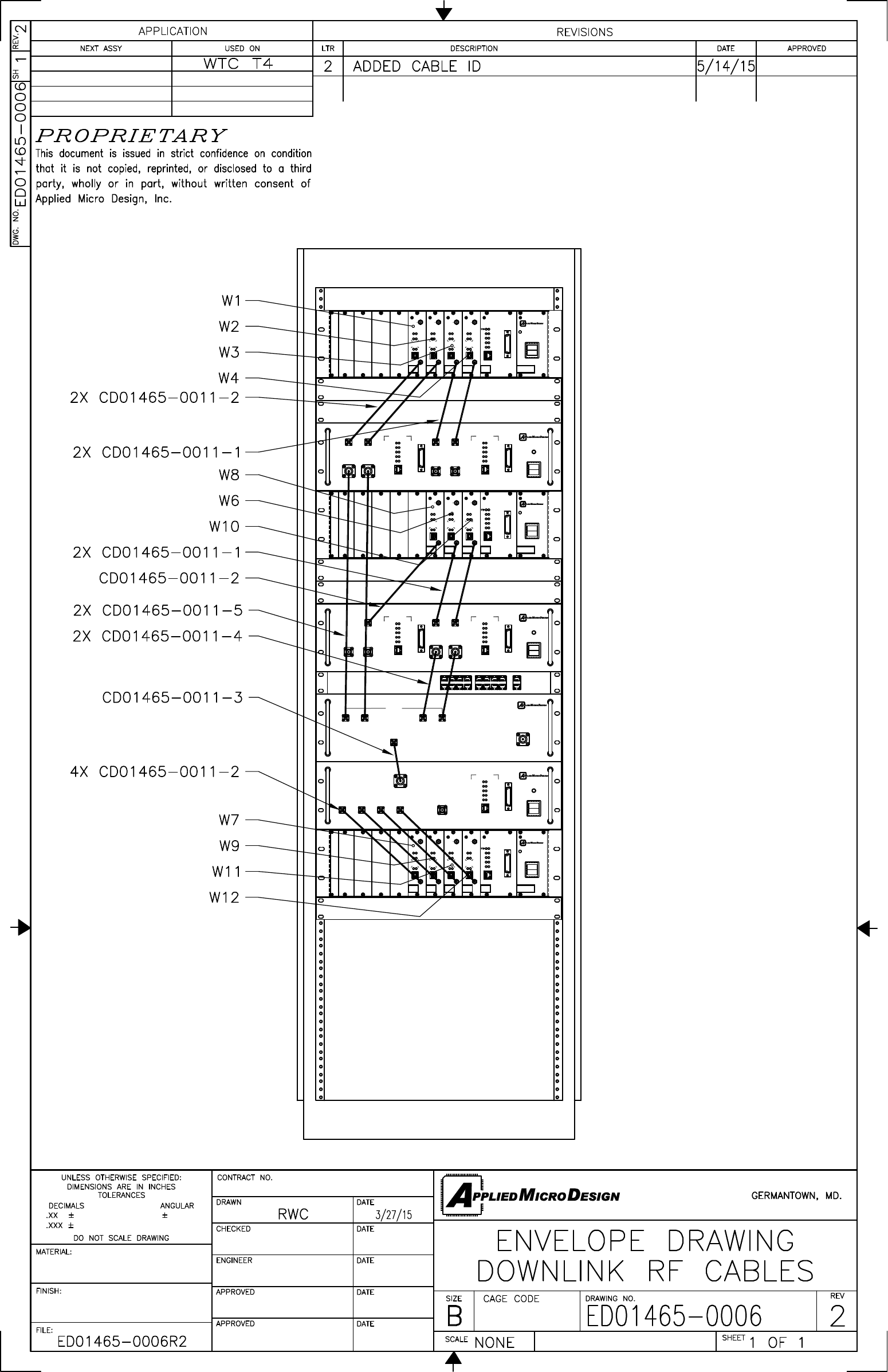
W4
W3
W2
W1
FLT
FLT
FLT
PWR
FLT
POWER
POWER
SUPPLY
RF OUT
RF IN
TX
READY
RX
1
1
1
2
2
2
RF OUT
RF IN
TX
READY
RX
1
1
1
2
2
2
RF OUT
RF IN
TX
READY
RX
1
1
1
2
2
2
ETHERNET
W4
W3
W2
W1
FLT
FLT
FLT
PWR
FLT
POWER
POWER
SUPPLY
RF OUT
RF IN
TX
READY
RX
1
1
1
2
2
2
RF OUT
RF IN
TX
READY
RX
1
1
1
2
2
2
RF OUT
RF IN
TX
READY
RX
1
1
1
2
2
2
RF OUT
RF IN
TX
READY
RX
1
1
1
2
2
2
ETHERNET
W4
W3
W2
W1
FLT
FLT
FLT
PWR
FLT
ETHERNET
FAN
STATUS
CURRENT
TEMP
FWD PWR
FAN FLT
KEY
REFL PWR
CURRENT FLT
TEMP FLT POWER
ETHERNET
TEMP
FAN
CURRENT
FWD PWR
STATUS
REFL PWR
CURRENT FLT
TEMP FLT
FAN FLT
KEY
IN1 IN2 IN3 IN4
OUT1 OUT2
482 - 485 MHz
W1 - W3
460 - 464 MHz
W4
SAMPLE2SAMPLE1
400 MHz DUAL AMPLIFIER
MODEL 1465PAD-3-1-400
RACS RACS
ETHERNET
FAN
STATUS
CURRENT
TEMP
FWD PWR
FAN FLT
KEY
REFL PWR
CURRENT FLT
TEMP FLT
ETHERNET
TEMP
FAN
CURRENT
FWD PWR
STATUS
REFL PWR
CURRENT FLT
TEMP FLT
FAN FLT
KEY
IN1 IN2 IN3
OUT3 OUT4
477 - 479 MHz
W8
453 - 454 MHz
W6 W10
SAMPLE2SAMPLE1
MODEL 1465PAD-2-1-400
400 MHz DUAL AMPLIFIER
POWER
RACS RACS
ETHERNET
FAN
STATUS
CURRENT
TEMP
FWD PWR
FAN FLT
KEY
REFL PWR
CURRENT FLT
TEMP FLT
IN1 IN2 IN3
OUT
IN4
851 - 854 MHz
W7 W9 W11 W12
SAMPLE
MODEL 1465PAS -4-800
800 MHz AMPLIFIER
POWER
RACS
IN 5
OUT
IN 3 IN 4
IN 1 IN 2
400 MHz
800 MHz
DOWNLINK CBC/COMBINER
MODEL 1465CCS-4-400
FAN TRAY
FAN TRAY
ETHERNET
CHANNEL CARD ASSEMBLY
400 MHz DUAL AMPLIFIER
MODEL NO. 1465PAD-3-1-400
CHANNEL CARD ASSEMBLY
MODEL NO. 1465DSP-3-2-P
400 MHz DUAL AMPLIFIER
MODEL NO. 1465PAD-2-1-400
MODEL NO. 1465DSP-4-2-P
CHANNEL CARD ASSEMBLY
MODEL NO. 1465PAS-4-800
800 MHz AMPLIFIER
MODEL NO. 1465CCS-4-400
DOWNLINK CBC/COMBINER
POWER
POWER
SUPPLY
RF OUT
RF IN
TX
READY
RX
1
1
1
2
2
2
RF OUT
RF IN
TX
READY
RX
1
1
1
2
2
2
RF OUT
RF IN
TX
READY
RX
1
1
1
2
2
2
RF OUT
RF IN
TX
READY
RX
1
1
1
2
2
2
ETHERNET
W4
W3
W2
W1
FLT
FLT
FLT
PWR
FLT
POWER
POWER
SUPPLY
RF OUT
RF IN
TX
READY
RX
1
1
1
2
2
2
RF OUT
RF IN
TX
READY
RX
1
1
1
2
2
2
RF OUT
RF IN
TX
READY
RX
1
1
1
2
2
2
ETHERNET
W4
W3
W2
W1
FLT
FLT
FLT
PWR
FLT
POWER
POWER
SUPPLY
RF OUT
RF IN
TX
READY
RX
1
1
1
2
2
2
RF OUT
RF IN
TX
READY
RX
1
1
1
2
2
2
RF OUT
RF IN
TX
READY
RX
1
1
1
2
2
2
RF OUT
RF IN
TX
READY
RX
1
1
1
2
2
2
ETHERNET
W4
W3
W2
W1
FLT
FLT
FLT
PWR
FLT
RF IN
OUT 1A OUT 1 OUT 2 OUT 3 OUT 4 OUT 5 OUT 7 OUT 10
OUT 8 OUT 9 OUT 11
400 MHz
800 MHz
MODEL 1465CSD-8-400-3-800
UPLINK DUAL CBC/SPLITTER
ETHERNET
AMPL2
AMPL1
RACS
POWER
PC RACK MOUNT
MONITOR & KEYBOARD
FAN TRAY
FAN TRAY
FAN TRAY
CHANNEL CARD ASSEMBLY
MODEL NO. 1465DSP-4-2-P
CHANNEL CARD ASSEMBLY
MODEL NO. 1465DSP-4-2-P
CHANNEL CARD ASSEMBLY
MODEL NO. 1465DSP-3-2-P
UPLINK DUAL CBC/SPLITTER
MODEL NO. 1465CSD-8-400-3-800
Back to Index
POWER
POWER
SUPPLY
A
PPLIED
M
ICRO ESIGN
D
RF OUT
RF IN
TX
READY
RX
1
1
1
2
2
2
RF OUT
RF IN
TX
READY
RX
1
1
1
2
2
2
RF OUT
RF IN
TX
READY
RX
1
1
1
2
2
2
RF OUT
RF IN
TX
READY
RX
1
1
1
2
2
2
ETHERNET
W4
W3
W2
STA
W1
FLT
FLT
FLT
PWR
FLT
Card No.
4
Card No.
3
Card No.
2
Card No.
1
Processor
Card
Power
Supply
DSP Card Cage - 4 Cards
Model No. 1465DSP-4-2-P
Card No.
3
Card No.
2
Card No.
1
Processor
Card
Power
Supply
DSP Card Cage - 3 Cards
Model No. 1465DSP-3-2-P
POWER
POWER
SUPPLY
A
PPLIED
M
ICRO ESIGN
D
RF OUT
RF IN
TX
READY
RX
1
1
1
2
2
2
RF OUT
RF IN
TX
READY
RX
1
1
1
2
2
2
RF OUT
RF IN
TX
READY
RX
1
1
1
2
2
2
ETHERNET
W4
W3
W2
STA
W1
FLT
FLT
FLT
PWR
FLT
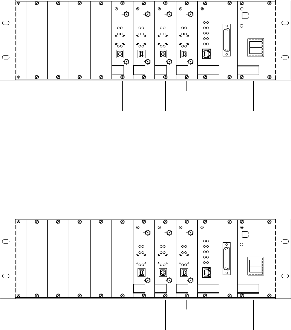
DSP Front Panel and Indicators
ETHERNET
W4
W3
W2
STA
W1
FLT
FLT
FLT
PWR
FLT
RACS
DSP Card
Processor Card
Status
Indicator
RF Output
Connector
USB
Connector
RF Input
Connector
RACS
Connector
MCAS
Connector
Status
Indicators
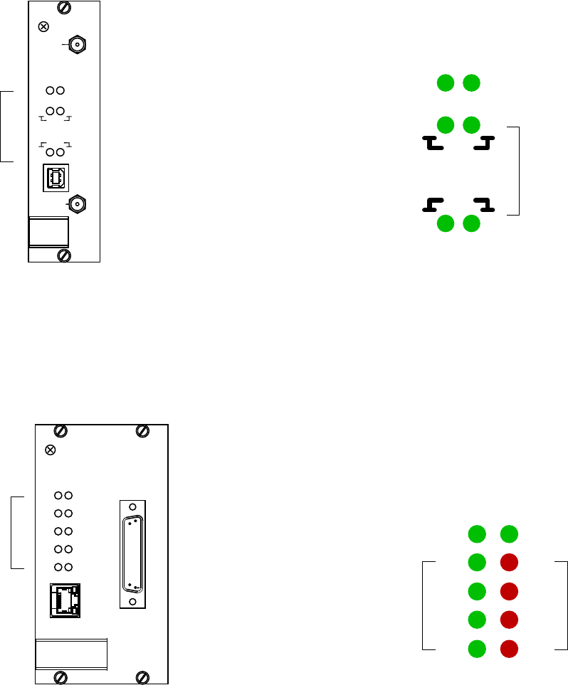
STATUS
1 2
1 2
1 2
RX
TX
STA
W1
W2
W3
W4
PWR
FLT
FLT
FLT
FLT
blinking: unit is operating steady: unit is powered
steady: either current,
reverse power or
temperature fault
blinking: card is disabled
steady: card is enabled
L.E.D. columns blink alternately until processor card
establishes communication with DSP cards.
steady: board is initialized
steady: board is keyed
blinking: board is communicating
with processor card
RF OUT
RF IN
TX
STATUS
RX
1
1
1
2
2
2
DSP Front Panel and Indicators
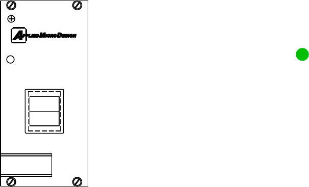
POWER
POWER
SUPPLY
Power Supply
Power
Indicator
Power
Switch
POWER
steady: unit is powered
The Channel Card is a Software Defined Radio (SDR) that can process up to sixteen
channels.
The filter parameters of each channel can be independently selected to optimize the Adjacent
Channel Time Delay Interference (TDI).
The FPGA-based design allows for the implementation of a number of Finite Impulse
Response (FIR) and Infinite Impulse Response (IIR) filters, including Cauer, Butterworth, and
Tchbecheff. All filters can be configured with the number of poles required to provide optimum
rejection, within the constraints of bandwidth and filter roll-off, to reduce or eliminate TDI.
Model 1465DSP is a two slot solution to channelized filtering for DAS systems. Two slot
receptions enable the filtering, AGC and Key Line control in two 12.5 kHz channels on one
channel card. TDMA and FDMA formats can be supported.
Parameters are adjustable using a Graphical User Interface (GUI) that runs on a laptop tied to
the USB front panel connector. The GUI enables the setting of center frequency, bandwidth,
threshold of operation, and Keying (CD, PL, or DPL). All channel parameters are stored in
non-volatile memory and the board will power up in the last programmed configuration. The
GUI will run on any laptop under Windows XP or later versions.

(all parameters are software defined)
Frequency Range Downlink Uplink
453 - 454 MHz 458 - 459 MHz
460 - 461 MHz 455 - 456 MHz
464 - 465 MHz 469 - 470 MHz
470 - 471 MHz 473 - 474 MHz
Number of Channels 2 (standard); optional 4, 8, 16 available
Channel Bandwidth 12.5 kHz or 25 kHz
Channel Spacing 12.5 kHz or 25 kHz
RF Frequency Accuracy tracks input signal exactly
Adjacent Channel Selectivity 50 dB @ +/- 17.5 kHz
Time Delay < 60 microseconds
Variation of Output Power with Input Level +0, -1.0 dB in either direction
AGC Time Constant < 100 microseconds
AGC Control Range + 80 dB
Maximum passband Ripple (Full Band) 2 dB (across full band)
Maximum Passband Ripple (Segment) 0.1 dB (across any 100 kHz segment)
IP3 +20 dBm
Keying PL, DPL, Carrier-Detect (computer control)
Duty Cycle Continuous
Operating Temperature Range -20 oC to +60 oC
Input / Output Impedance 50 Ohms
Input / Output VSWR 1.35:1, worst-case
Input / Output Connectors SMA
Input Power 95 - 132 VAC, 45 - 64 Hz
**
** - VHF, 800 MHz, and 900 MHz also available
DSP Specifications
Back to Index
Power
Switch
Power
Indicator
RACS
Connector
RACS
Connector
Input 3
Connector
Input 2
Connector
Input 1
Connector
-40 dB
Sample Port 2
Connector
-40 dB
Sample Port 1
Connector
MCAS
Ethernet
Connector
MCAS
Ethernet
Connector
Output 1
Connector
Output 2
Connector
192.168.7.xxx
IP Address
192.168.7.xxx
IP Address
STATUS KEY
REFL PWR
CURRENT FLT
TEMP FLT
FAN FLT
FWD PWR
CURRENT
TEMP
FAN
ETHERNET
FAN
STATUS
CURRENT
TEMP
FWD PWR
FAN FLT
KEY
REFL PWR
CURRENT FLT
TEMP FLT POWER
ETHERNET
TEMP
FAN
CURRENT
FWD PWR
STATUS
REFL PWR
CURRENT FLT
TEMP FLT
FAN FLT
KEY
IN1 IN2 IN3 IN4
OUT1 OUT2
482 - 485 MHz
W1 - W3
460 - 464 MHz
W4
SAMPLE2SAMPLE1
400 MHz DUAL AMPLIFIER
MODEL 1465PAD-3-1-400
RACS RACS
Dual Power Amplifier - Front Panel and Indicators
Model No. 1465PAD-3-1-400
Input 4
Connector
steady: amplifer is operating steady: amplifier is enabled
steady: amplifier is operating
normally
steady: amplifier has either
current, reverse power or
temperature fault
ETHERNET
FAN
STATUS
CURRENT
TEMP
FWD PWR
FAN FLT
KEY
REFL PWR
CURRENT FLT
TEMP FLT
ETHERNET
TEMP
FAN
CURRENT
FWD PWR
STATUS
REFL PWR
CURRENT FLT
TEMP FLT
FAN FLT
KEY
IN1 IN2 IN3
OUT3 OUT4
477 - 479 MHz
W8
453 - 454 MHz
W6 W10
SAMPLE2SAMPLE1
MODEL 1465PAD-2-1-400
400 MHz DUAL AMPLIFIER
A
PPLIEDMICRO ESIGND
POWER
RACS RACS
Power
Switch
Power
Indicator
RACS
Connector
RACS
Connector
Input 2
Connector
Input 1
Connector
-40 dB
Sample Port 2
Connector
-40 dB
Sample Port 1
Connector
MCAS
Ethernet
Connector
MCAS
Ethernet
Connector
Output 3
Connector
Output 4
Connector
192.168.7.xxx
IP Address
192.168.7.xxx
IP Address
Input 3
Connector
Dual Power Amplifier - Front Panel and Indicators
Model No. 1465PAD-2-1-400
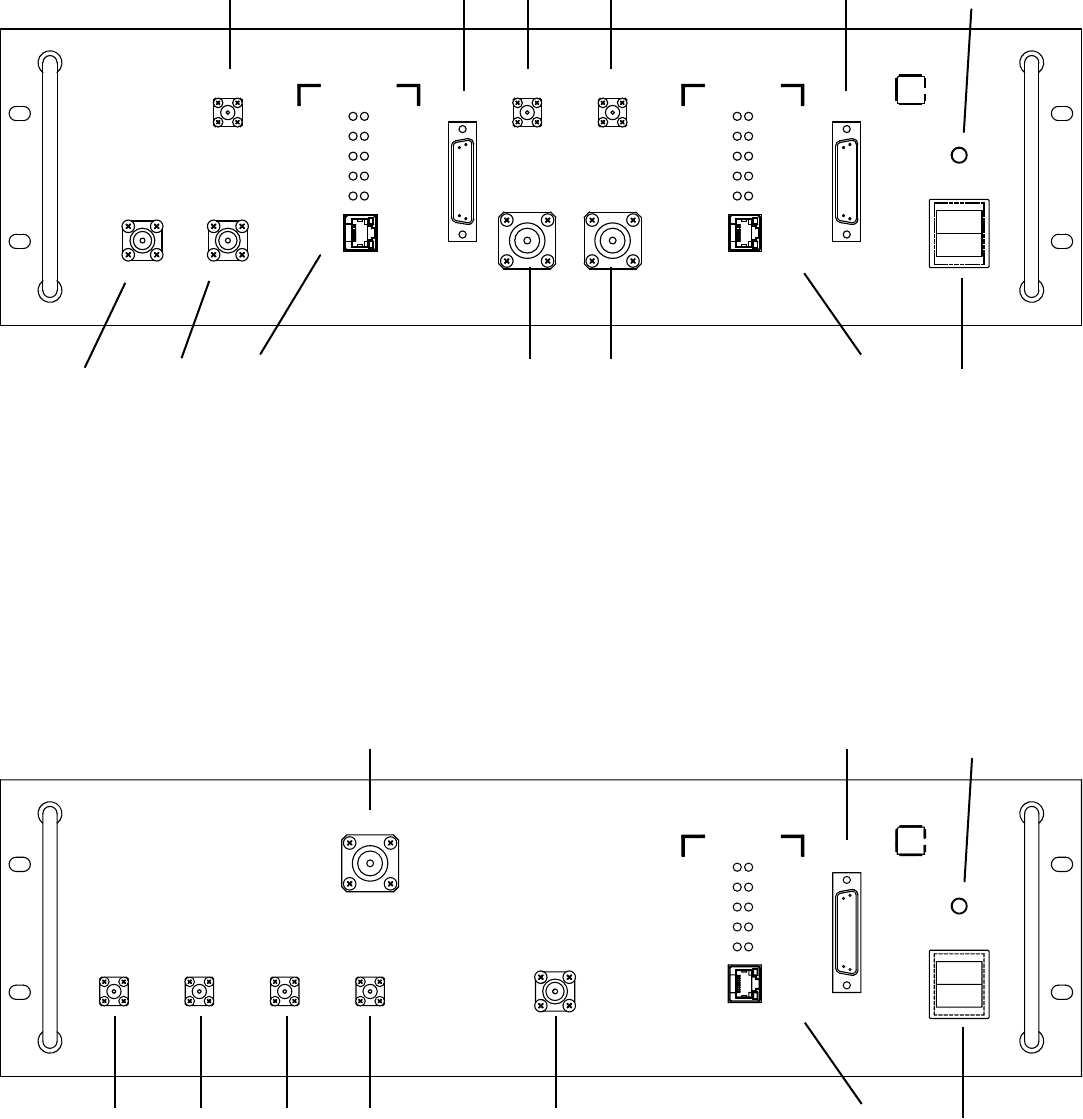
Single Power Amplifier - Front Panel and Indicators
Model No. 1465PAS-4-800
ETHERNET
FAN
STATUS
CURRENT
TEMP
FWD PWR
FAN FLT
KEY
REFL PWR
CURRENT FLT
TEMP FLT
IN1 IN2 IN3
OUT
IN4
851 - 854 MHz
W7 W9 W11 W12
SAMPLE
MODEL 1465PAS-4-800
800 MHz AMPLIFIER
A
PPLIED
M
ICRO ESIGN
D
POWER
RACS
Power
Switch
Power
Indicator
RACS
Connector
Input 2
Connector
-40 dB
Sample Port
Connector
MCAS
Ethernet
Connector
Output 3
Connector
192.168.7.xxx
IP Address
Input 3
Connector
Input 4
Connector
Input 1
Connector

Power Amplifier Specifications
Frequency: 851 - 854 MHz
Power Output: 6.5 W (+38 dBm) Composite
Power Output: + 22 dBm / carrier
Gain: 35 - 45 dB
Gain Adjust: 10 dB
ALC: 5 Watts
OIP3: +60 dBm
Impedance: 50 Ohms
Load VSWR: Infinite, no damage
N.F.: 7 dB
Power Supply: 110V AC
Current: < 2A
Operating Temp: -30° to +60° C
Size: 19” x 5.22” x 16”
Frequency: 453 - 488 MHz
Power Output: 5 W (+37 dBm) Composite
Power Output: + 20 dBm / carrier
Gain: 35 - 45 dB
Gain Adjust: 10 dB
ALC: 5 Watts
OIP3: +55 dBm
Impedance: 50 Ohms
Load VSWR: Infinite, no damage
N.F.: 7 dB
Power Supply: 110V AC
Current: < 2A
Operating Temp: -30° to +60° C
Size: 19” x 5.22” x 16”
The 1465PA channel amplifier is a high-linearity, multi-carrier amplifier for DAS (Distributed
Antenna System) applications. The unit is a single or dual-amplifier configuration. Each
amplifier has its own processor board, alarms, panel indicators and power supply. The
processor board controls the enable signal to the amplifier and monitors forward power, reverse
power, current, fan status and heat sink temperature.
The processor board features remote monitoring capability via Ethernet. A computer running
the Graphical User Interface (GUI) can display the status of the amplifier and provide control.
A front panel Look Port for each amplifier allows the user to sample the signal at the front
panel. Look port enables measurement without interrupting main line communications. The
Look Port sample is 40 dB below the main RF output port.
The processor board contains six NO/NC relay lines that interface to any alarm system and
control.
Back to Index
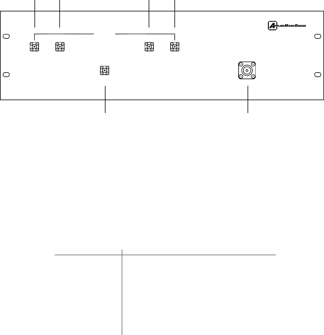
CBC/Combiner - Front Panel
Model No. 1465CCS-4-400
IN 5
OUT
IN 3 IN 4
IN 1 IN 2
400 MHz
800 MHz
Input 2
Connector
Output
Connector
Input 3
Connector
Input 4
Connector
Input 1
Connector
Input 5
Connector
The 1465CCS-4-400 is a Cross Band Coupler (CBC) and Combiner in one chassis;
it is designed for DAS (Distributed Antenna System) applications. The low-insertion
loss CBC combines signals from two paths; 400 MHz and 800 MHz bands. The 400
MHz band path has a combiner prior to the CBC for multi-channel combining of
multi-carrier signals.
Frequency: 453 - 488 MHz; 851 - 854 MHz
Input Power: 40 dBm (10W) each port maximum
Insertion Loss: < 2 dB
Isolation: 40 dB minimum between ports
Impedance: 50 Ohms
Operating Temp: -30 to +60 °C
Input Connectors: SMA female
Output Connector: N-type female
Size: 19” x 5.22” x 12”
CBC/Combiner Specifications
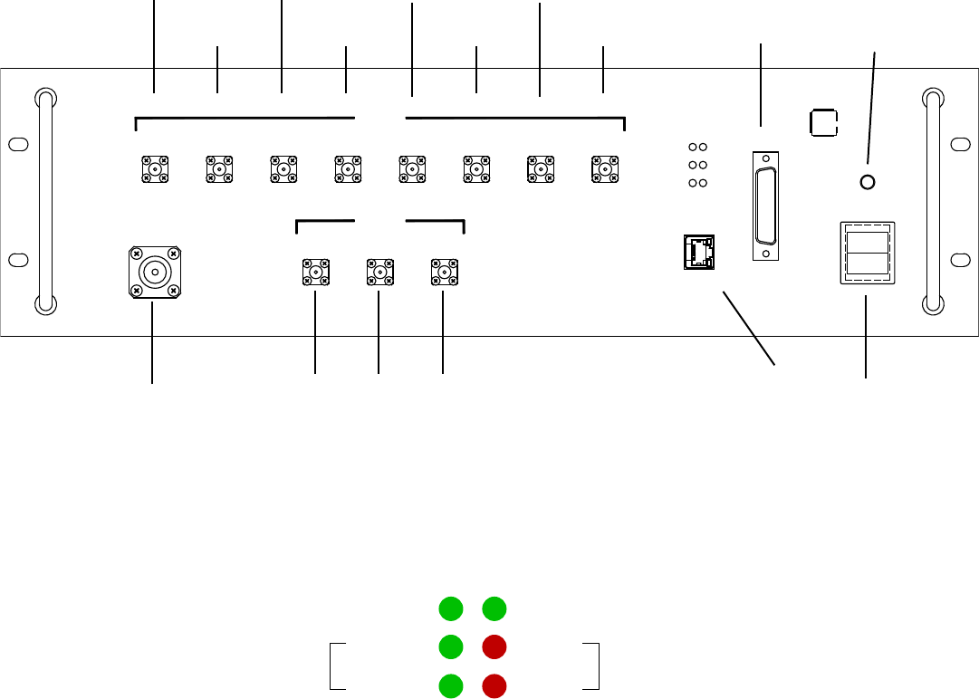
CBC/Splitter - Front Panel and Indicators
Model No. 1465CSD-8-400-3-800
Power
Switch
Power
Indicator
RACS
Connector
MCAS
Ethernet
Connector
Output 1A
Connector
192.168.7.xxx
IP Address
Input
Connector
Output 8
Connector
Output 9
Connector
Output 11
Connector
Output 1
Connector
Output 2
Connector
Output 3
Connector
Output 4
Connector
Output 5
Connector
Output 7
Connector
Output 10
Connector
RF IN
OUT 1A OUT 1 OUT 2 OUT 3 OUT 4 OUT 5 OUT 7 OUT 10
OUT 8 OUT 9 OUT 11
400 MHz
800 MHz
MODEL 1465CSD-8-400-3-800
UPLINK CBC/SPLITTER
A
PPLIED MICRO ESIGND
ETHERNET
AMPL2
AMPL1
RACS
POWER
STA PWR
STA PWR
AMPL1
AMPL2
blinking: LNAs are operating steady: LNAs are powered
steady: LNAs are operating
normally steady: LNA has current fault

Frequency: 458 - 488 MHz; 806 - 809 MHz
Input Power: 40 dBm (10W) maximum
Gain: 10 dB
Noise Figure: < 2 dB
Isolation: 60 dB minimum between ports
Impedance: 50 Ohms
Input Connector: N-type female
Output Connector: SMA female
Power Supply: 110V AC
Current: < 1 A
Operating Temp: -30 to +60 °C
Size: 19” x 5.22” x 16”
CBC/Splitter Specifications
The 1465CSD-8-400-3-800 is a Cross Band Coupler and Splitter housed in one chassis;
it is designed for DAS (Distributed Antenna System) applications. The CBC/Splitter
separates signals from the 400 MHz and 800 MHz bands into two paths. Each path has
a splitter for multi-channel distribution of multi-carrier signals for downstream processing.
A Low-Noise Amplifier (LNA) in front of each splitter provides improved signal-to-noise
ratio (SNR) at the splitter outputs. The LNAs are tied to a processor board that functions
as a current monitor. The processor board provides status via front-panel LEDs and
also features a remote monitoring capability via Ethernet. A computer running the
Graphical User Interface (GUI) can display the status of the amplifiers.
Back to Index
MODEL NO. 1465DSP-4-2-P
POWER
POWER
SUPPLY
RF OUT
RF IN
TX
READY
RX
1
1
1
2
2
2
RF OUT
RF IN
TX
READY
RX
1
1
1
2
2
2
RF OUT
RF IN
TX
READY
RX
1
1
1
2
2
2
RF OUT
RF IN
TX
READY
RX
1
1
1
2
2
2
ETHERNET
W4
W3
W2
W1
FLT
FLT
FLT
PWR
FLT
POWER
POWER
SUPPLY
RF OUT
RF IN
TX
READY
RX
1
1
1
2
2
2
RF OUT
RF IN
TX
READY
RX
1
1
1
2
2
2
RF OUT
RF IN
TX
READY
RX
1
1
1
2
2
2
ETHERNET
W4
W3
W2
W1
FLT
FLT
FLT
PWR
FLT
POWER
POWER
SUPPLY
RF OUT
RF IN
TX
READY
RX
1
1
1
2
2
2
RF OUT
RF IN
TX
READY
RX
1
1
1
2
2
2
RF OUT
RF IN
TX
READY
RX
1
1
1
2
2
2
RF OUT
RF IN
TX
READY
RX
1
1
1
2
2
2
ETHERNET
W4
W3
W2
W1
FLT
FLT
FLT
PWR
FLT
ETHERNET
FAN
STATUS
CURRENT
TEMP
FWD PWR
FAN FLT
KEY
REFL PWR
CURRENT FLT
TEMP FLT POWER
ETHERNET
TEMP
FAN
CURRENT
FWD PWR
STATUS
REFL PWR
CURRENT FLT
TEMP FLT
FAN FLT
KEY
IN1 IN2 IN3 IN4
OUT1 OUT2
482 - 485 MHz
W1 - W3
460 - 464 MHz
W4
SAMPLE2SAMPLE1
400 MHz DUAL AMPLIFIER
MODEL 1465PAD-3-1-400
RACS RACS
ETHERNET
FAN
STATUS
CURRENT
TEMP
FWD PWR
FAN FLT
KEY
REFL PWR
CURRENT FLT
TEMP FLT
ETHERNET
TEMP
FAN
CURRENT
FWD PWR
STATUS
REFL PWR
CURRENT FLT
TEMP FLT
FAN FLT
KEY
IN1 IN2 IN3
OUT3 OUT4
477 - 479 MHz
W8
453 - 454 MHz
W6 W10
SAMPLE2SAMPLE1
MODEL 1465PAD-2-1-400
400 MHz DUAL AMPLIFIER
POWER
RACS RACS
ETHERNET
FAN
STATUS
CURRENT
TEMP
FWD PWR
FAN FLT
KEY
REFL PWR
CURRENT FLT
TEMP FLT
IN1 IN2 IN3
OUT
IN4
851 - 854 MHz
W7 W9 W11 W12
SAMPLE
MODEL 1465PAS -4-800
800 MHz AMPLIFIER
POWER
RACS
IN 5
OUT
IN 3 IN 4
IN 1 IN 2
400 MHz
800 MHz
DOWNLINK CBC/COMBINER
MODEL 1465CCS-4-400
FAN TRAY
FAN TRAY
ETHERNET
CHANNEL CARD ASSEMBLY
400 MHz DUAL AMPLIFIER
MODEL NO. 1465PAD-3-1-400
CHANNEL CARD ASSEMBLY
MODEL NO. 1465DSP-3-2-P
400 MHz DUAL AMPLIFIER
MODEL NO. 1465PAD-2-1-400
MODEL NO. 1465DSP-4-2-P
CHANNEL CARD ASSEMBLY
MODEL NO. 1465PAS-4-800
800 MHz AMPLIFIER
MODEL NO. 1465CCS-4-400
DOWNLINK CBC/COMBINER
POWER
POWER
SUPPLY
RF OUT
RF IN
TX
READY
RX
1
1
1
2
2
2
RF OUT
RF IN
TX
READY
RX
1
1
1
2
2
2
RF OUT
RF IN
TX
READY
RX
1
1
1
2
2
2
RF OUT
RF IN
TX
READY
RX
1
1
1
2
2
2
ETHERNET
W4
W3
W2
W1
FLT
FLT
FLT
PWR
FLT
POWER
POWER
SUPPLY
RF OUT
RF IN
TX
READY
RX
1
1
1
2
2
2
RF OUT
RF IN
TX
READY
RX
1
1
1
2
2
2
RF OUT
RF IN
TX
READY
RX
1
1
1
2
2
2
ETHERNET
W4
W3
W2
W1
FLT
FLT
FLT
PWR
FLT
POWER
POWER
SUPPLY
RF OUT
RF IN
TX
READY
RX
1
1
1
2
2
2
RF OUT
RF IN
TX
READY
RX
1
1
1
2
2
2
RF OUT
RF IN
TX
READY
RX
1
1
1
2
2
2
RF OUT
RF IN
TX
READY
RX
1
1
1
2
2
2
ETHERNET
W4
W3
W2
W1
FLT
FLT
FLT
PWR
FLT
RF IN
OUT 1A OUT 1 OUT 2 OUT 3 OUT 4 OUT 5 OUT 7 OUT 10
OUT 8 OUT 9 OUT 11
400 MHz
800 MHz
MODEL 1465CSD-8-400-3-800
UPLINK DUAL CBC/SPLITTER
ETHERNET
AMPL2
AMPL1
RACS
POWER
PC RACK MOUNT
MONITOR & KEYBOARD
FAN TRAY
FAN TRAY
FAN TRAY
CHANNEL CARD ASSEMBLY
MODEL NO. 1465DSP-4-2-P
CHANNEL CARD ASSEMBLY
MODEL NO. 1465DSP-4-2-P
CHANNEL CARD ASSEMBLY
MODEL NO. 1465DSP-3-2-P
UPLINK DUAL CBC/SPLITTER
MODEL NO. 1465CSD-8-400-3-800
Back to Index
MODEL NO. 1465DSP-4-2-P
POWER
POWER
SUPPLY
RF OUT
RF IN
TX
READY
RX
1
1
1
2
2
2
RF OUT
RF IN
TX
READY
RX
1
1
1
2
2
2
RF OUT
RF IN
TX
READY
RX
1
1
1
2
2
2
RF OUT
RF IN
TX
READY
RX
1
1
1
2
2
2
ETHERNET
W4
W3
W2
W1
FLT
FLT
FLT
PWR
FLT
POWER
POWER
SUPPLY
RF OUT
RF IN
TX
READY
RX
1
1
1
2
2
2
RF OUT
RF IN
TX
READY
RX
1
1
1
2
2
2
RF OUT
RF IN
TX
READY
RX
1
1
1
2
2
2
ETHERNET
W4
W3
W2
W1
FLT
FLT
FLT
PWR
FLT
POWER
POWER
SUPPLY
RF OUT
RF IN
TX
READY
RX
1
1
1
2
2
2
RF OUT
RF IN
TX
READY
RX
1
1
1
2
2
2
RF OUT
RF IN
TX
READY
RX
1
1
1
2
2
2
RF OUT
RF IN
TX
READY
RX
1
1
1
2
2
2
ETHERNET
W4
W3
W2
W1
FLT
FLT
FLT
PWR
FLT
ETHERNET
FAN
STATUS
CURRENT
TEMP
FWD PWR
FAN FLT
KEY
REFL PWR
CURRENT FLT
TEMP FLT POWER
ETHERNET
TEMP
FAN
CURRENT
FWD PWR
STATUS
REFL PWR
CURRENT FLT
TEMP FLT
FAN FLT
KEY
IN1 IN2 IN3 IN4
OUT1 OUT2
482 - 485 MHz
W1 - W3
460 - 464 MHz
W4
SAMPLE2SAMPLE1
400 MHz DUAL AMPLIFIER
MODEL 1465PAD-3-1-400
RACS RACS
ETHERNET
FAN
STATUS
CURRENT
TEMP
FWD PWR
FAN FLT
KEY
REFL PWR
CURRENT FLT
TEMP FLT
ETHERNET
TEMP
FAN
CURRENT
FWD PWR
STATUS
REFL PWR
CURRENT FLT
TEMP FLT
FAN FLT
KEY
IN1 IN2 IN3
OUT3 OUT4
477 - 479 MHz
W8
453 - 454 MHz
W6 W10
SAMPLE2SAMPLE1
MODEL 1465PAD-2-1-400
400 MHz DUAL AMPLIFIER
POWER
RACS RACS
ETHERNET
FAN
STATUS
CURRENT
TEMP
FWD PWR
FAN FLT
KEY
REFL PWR
CURRENT FLT
TEMP FLT
IN1 IN2 IN3
OUT
IN4
851 - 854 MHz
W7 W9 W11 W12
SAMPLE
MODEL 1465PAS -4-800
800 MHz AMPLIFIER
POWER
RACS
IN 5
OUT
IN 3 IN 4
IN 1 IN 2
400 MHz
800 MHz
DOWNLINK CBC/COMBINER
MODEL 1465CCS-4-400
FAN TRAY
FAN TRAY
ETHERNET
CHANNEL CARD ASSEMBLY
400 MHz DUAL AMPLIFIER
MODEL NO. 1465PAD-3-1-400
CHANNEL CARD ASSEMBLY
MODEL NO. 1465DSP-3-2-P
400 MHz DUAL AMPLIFIER
MODEL NO. 1465PAD-2-1-400
MODEL NO. 1465DSP-4-2-P
CHANNEL CARD ASSEMBLY
MODEL NO. 1465PAS-4-800
800 MHz AMPLIFIER
MODEL NO. 1465CCS-4-400
DOWNLINK CBC/COMBINER
TO UPLINK RACK
POWER
POWER
SUPPLY
RF OUT
RF IN
TX
READY
RX
1
1
1
2
2
2
RF OUT
RF IN
TX
READY
RX
1
1
1
2
2
2
RF OUT
RF IN
TX
READY
RX
1
1
1
2
2
2
RF OUT
RF IN
TX
READY
RX
1
1
1
2
2
2
ETHERNET
W4
W3
W2
W1
FLT
FLT
FLT
PWR
FLT
POWER
POWER
SUPPLY
RF OUT
RF IN
TX
READY
RX
1
1
1
2
2
2
RF OUT
RF IN
TX
READY
RX
1
1
1
2
2
2
RF OUT
RF IN
TX
READY
RX
1
1
1
2
2
2
ETHERNET
W4
W3
W2
W1
FLT
FLT
FLT
PWR
FLT
POWER
POWER
SUPPLY
RF OUT
RF IN
TX
READY
RX
1
1
1
2
2
2
RF OUT
RF IN
TX
READY
RX
1
1
1
2
2
2
RF OUT
RF IN
TX
READY
RX
1
1
1
2
2
2
RF OUT
RF IN
TX
READY
RX
1
1
1
2
2
2
ETHERNET
W4
W3
W2
W1
FLT
FLT
FLT
PWR
FLT
RF IN
OUT 1A OUT 1 OUT 2 OUT 3 OUT 4 OUT 5 OUT 7 OUT 10
OUT 8 OUT 9 OUT 11
400 MHz
800 MHz
MODEL 1465CSD-8-400-3-800
UPLINK DUAL CBC/SPLITTER
ETHERNET
AMPL2
AMPL1
RACS
POWER
PC RACK MOUNT
MONITOR & KEYBOARD
FAN TRAY
FAN TRAY
FAN TRAY
CHANNEL CARD ASSEMBLY
MODEL NO. 1465DSP-4-2-P
CHANNEL CARD ASSEMBLY
MODEL NO. 1465DSP-4-2-P
CHANNEL CARD ASSEMBLY
MODEL NO. 1465DSP-3-2-P
UPLINK DUAL CBC/SPLITTER
MODEL NO. 1465CSD-8-400-3-800
FROM DOWNLINK RACK
Back to Index
PPLIED MICRO ESIGND
POWER
POWER
SUPPLY
RF OUT
RF IN
TX
READY
RX
1
1
1
2
2
2
RF OUT
RF IN
TX
READY
RX
1
1
1
2
2
2
RF OUT
RF IN
TX
READY
RX
1
1
1
2
2
2
RF OUT
RF IN
TX
READY
RX
1
1
1
2
2
2
ETHERNET
W4
W3
W2
W1
FLT
FLT
FLT
PWR
FLT
POWER
POWER
SUPPLY
RF OUT
RF IN
TX
READY
RX
1
1
1
2
2
2
RF OUT
RF IN
TX
READY
RX
1
1
1
2
2
2
RF OUT
RF IN
TX
READY
RX
1
1
1
2
2
2
ETHERNET
W4
W3
W2
W1
FLT
FLT
FLT
PWR
FLT
POWER
POWER
SUPPLY
RF OUT
RF IN
TX
READY
RX
1
1
1
2
2
2
RF OUT
RF IN
TX
READY
RX
1
1
1
2
2
2
RF OUT
RF IN
TX
READY
RX
1
1
1
2
2
2
RF OUT
RF IN
TX
READY
RX
1
1
1
2
2
2
ETHERNET
W4
W3
W2
W1
FLT
FLT
FLT
PWR
FLT
ETHERNET
FAN
STATUS
CURRENT
TEMP
FWD PWR
FAN FLT
KEY
REFL PWR
CURRENT FLT
TEMP FLT POWER
ETHERNET
TEMP
FAN
CURRENT
FWD PWR
STATUS
REFL PWR
CURRENT FLT
TEMP FLT
FAN FLT
KEY
IN1 IN2 IN3 IN4
OUT1 OUT2
482 - 485 MHz
W1 - W3
460 - 464 MHz
W4
SAMPLE2SAMPLE1
400 MHz DUAL AMPLIFIER
MODEL 1465PAD-3-1-400
RACS RACS
ETHERNET
FAN
STATUS
CURRENT
TEMP
FWD PWR
FAN FLT
KEY
REFL PWR
CURRENT FLT
TEMP FLT
ETHERNET
TEMP
FAN
CURRENT
FWD PWR
STATUS
REFL PWR
CURRENT FLT
TEMP FLT
FAN FLT
KEY
IN1 IN2 IN3
OUT3 OUT4
477 - 479 MHz
W8
453 - 454 MHz
W6 W10
SAMPLE2SAMPLE1
MODEL 1465PAD-2-1-400
400 MHz DUAL AMPLIFIER
POWER
RACS RACS
ETHERNET
FAN
STATUS
CURRENT
TEMP
FWD PWR
FAN FLT
KEY
REFL PWR
CURRENT FLT
TEMP FLT
IN1 IN2 IN3
OUT
IN4
851 - 854 MHz
W7 W9 W11 W12
SAMPLE
MODEL 1465PAS-4-800
800 MHz AMPLIFIER
POWER
RACS
IN 5
OUT
IN 3 IN 4
IN 1 IN 2
400 MHz
800 MHz
DOWNLINK CBC/COMBINER
MODEL 1465CCS-4-400
FAN TRAY
FAN TRAY
ETHERNET
Downlink Installation
Connect to
Distributed
Antenna System
(DAS)
No antennas, cables, and/or coupling devices are shipped with this equipment.
POWER
POWER
SUPPLY
RF OUT
RF IN
TX
READY
RX
1
1
1
2
2
2
RF OUT
RF IN
TX
READY
RX
1
1
1
2
2
2
RF OUT
RF IN
TX
READY
RX
1
1
1
2
2
2
RF OUT
RF IN
TX
READY
RX
1
1
1
2
2
2
ETHERNET
W4
W3
W2
W1
FLT
FLT
FLT
PWR
FLT
POWER
POWER
SUPPLY
RF OUT
RF IN
TX
READY
RX
1
1
1
2
2
2
RF OUT
RF IN
TX
READY
RX
1
1
1
2
2
2
RF OUT
RF IN
TX
READY
RX
1
1
1
2
2
2
ETHERNET
W4
W3
W2
W1
FLT
FLT
FLT
PWR
FLT
POWER
POWER
SUPPLY
RF OUT
RF IN
TX
READY
RX
1
1
1
2
2
2
RF OUT
RF IN
TX
READY
RX
1
1
1
2
2
2
RF OUT
RF IN
TX
READY
RX
1
1
1
2
2
2
RF OUT
RF IN
TX
READY
RX
1
1
1
2
2
2
ETHERNET
W4
W3
W2
W1
FLT
FLT
FLT
PWR
FLT
RF IN
OUT 1A OUT 1 OUT 2 OUT 3 OUT 4 OUT 5 OUT 7 OUT 10
OUT 8 OUT 9 OUT 11
400 MHz
800 MHz
MODEL 1465CSD-8-400-3-800
UPLINK DUAL CBC/SPLITTER
ETHERNET
AMPL2
AMPL1
RACS
POWER
PC RACK MOUNT
MONITOR & KEYBOARD
FAN TRAY
FAN TRAY
FAN TRAY
Uplink Installation
Connect to
Distributed
Antenna System
(DAS)
No antennas, cables, and/or coupling devices are shipped with this equipment.
Appendix A
NMS GUI Manual

USER’S
MANUAL
Network Monitoring and Control System 1.0 – AMDI
(NMS)
Applied Micro Design Inc.
May, 2015

Revision Sheet
NMS User’s Manual Page i
Revision Sheet
Release No.
Date
Revision Description
1.0
5/25/15
User’s Manual Created

NMS User’s Manual Page ii
USER'S MANUAL
TABLE OF CONTENTS
Page #
1.0 PRODUCT DESCRIPTION ............................................................. Error! Bookmark not defined.
1.1 Overview ................................................................................................................................1-1
1.2 Key Features...........................................................................................................................1-1
1.3 Acronyms and Abbreviations.................................................. Error! Bookmark not defined.
2.0 GETTING STARTED .....................................................................................................................2-1
2.1 Startup .................................................................................................................................... 2-1
2.2 System Requirements ............................................................................................................. 2.1
2.3 Opening the Map....................................................................................................................2-1
2.4 Exit NMS................................................................................................................................2-2
3.0 MAPS...............................................................................................................................................3-1
3.1 Overview Map........................................................................................................................3-1
3.2 Node View Map .....................................................................................................................3-2
4.0 COMPONENT LEVEL GUI ...........................................................................................................4-1
4.1 AMDI DSP Processor Board Control ....................................................................................4-1
4.1.1 Status/Control .........................................................................................................................4-1
4.1.2 Thresholds...............................................................................................................................4-2
4.1.3 Update.....................................................................................................................................4-3
4.1.4 Faults.......................................................................................................................................4-4
4.2 AMDI Power Amplifier Control ............................................................................................ 4-4
4.2.1 Status/Control .........................................................................................................................4-4
4.2.2 Thresholds...............................................................................................................................4-5
4.2.3 Update.....................................................................................................................................4-6
4.2.4 Faults.......................................................................................................................................4-7
4.3 AMDI Cross Band Coupler....................................................................................................4-7
4.3.1 Status.......................................................................................................................................4-7
4.3.2 Thresholds...............................................................................................................................4-8
4.3.3 Update.....................................................................................................................................4-9
4.3.4 Faults.....................................................................................................................................4-10

1.0 Product Description
NMS User’s Manual
1.0 PRODUCT DESCRIPTION

1.0 Product Description
NMS User’s Manual Page 1-1
1.0 PRODUCT DESCRIPTION
1.1 Overview
The WTC NMS is a graphical user interface, GUI, program that notifies WTC personnel if a specific
component fails or if a condition exists that can cause a failure. The GUI continuously polls each
component and displays the current status on the GUI screen. If a failure or adverse condition is
detected, an icon on the WTC NMS flashes red.
The WTC NMS consists of layered maps which provide different levels of detail. The user can double
click on a node, to see a more detailed view of the equipment or to identify a failed or about to fail
component.
1.2 Key Features
The important NMS features include the following:
This system indicates the device status whether normal, alarming, connected or disconnected.
Continuous polling updating status
Component management through Ethernet Interface
High-level view
Drill down windows to view more detailed information
Configurable Alarm Thresholds
Device enable/disable

1.0 Product Description
NMS User’s Manual Page 1-2
1.3 Acronyms and Abbreviations
WTC – World Trade Center. This is the site for the system installation.
GUI – Graphical User Interface
NMS – Network Management and Control System
AMDI – Applied Micro Design Inc.
DSP – Digital Signal Processing
RF – Radio Frequency
CBC – Cross Band Coupler
UI – User Interface
LNA – Low Noise Amplifier
PWR – Power
UL – Up Link
DL – Down Link

2.0 Getting Started
NMS User’s Manual
2.0 GETTING STARTED
2.0 Getting Started
NMS User’s Manual Page 2-1
2.0 GETTING STARTED
2.1 Startup
The system comes with the NMS pre-installed.
Start NMS server:
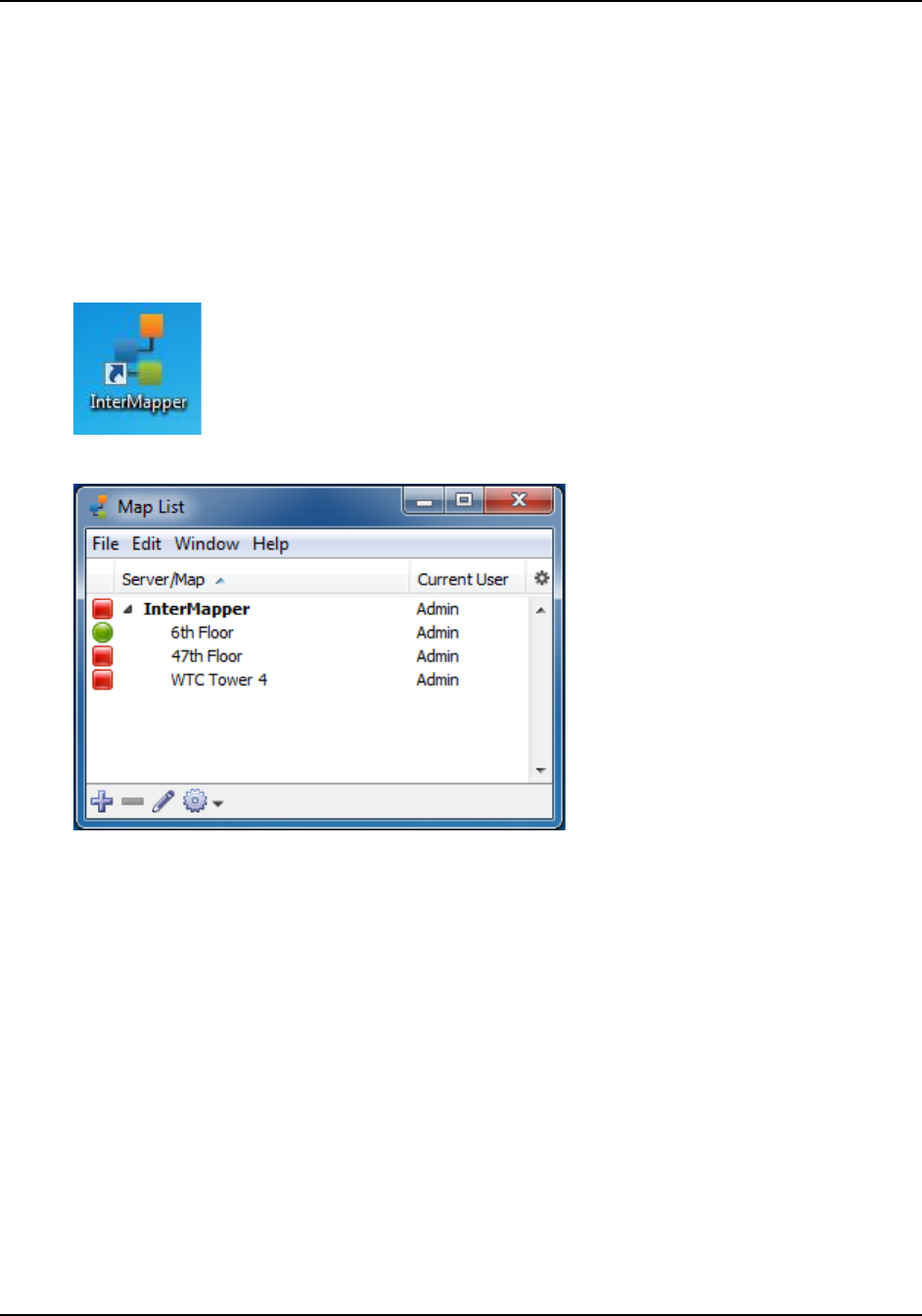
1. Double-click the Intermapper® icon on the Desktop.
Figure 2: InterMapper® Desktop Shortcut
2. The Map List window will appear.
Figure 3: Map List
2.2 System Requirements
To use NMS, ensure the following minimum software and Hardware requirements are available:
Hardware Requirements
oWindows 7 Operating System or greater.
oEthernet RJ-45 interface
Software Requirements – Intermapper® with a minimum license to monitor 50 devices.
2.3 Opening the Map
Double-click the ‘WTC Tower 4’ map. This will open the overview window which displays a high level
view of the entire system.

2.0 Getting Started
NMS User’s Manual Page 2-2
2.4 Exit NMS
Close all map windows, Intermapper® application, and component GUI windows.

3.0 Maps
NMS User’s Manual
3.0 MAPS

3.0 Maps
NMS User’s Manual Page 3-1
3.0 MAPS
The WTC NMS consists of layered maps which provide different levels of detail. The user can double
click on a node, to see a more detailed view of the equipment or to identify a failed or about to fail
component.
3.1 Overview Map
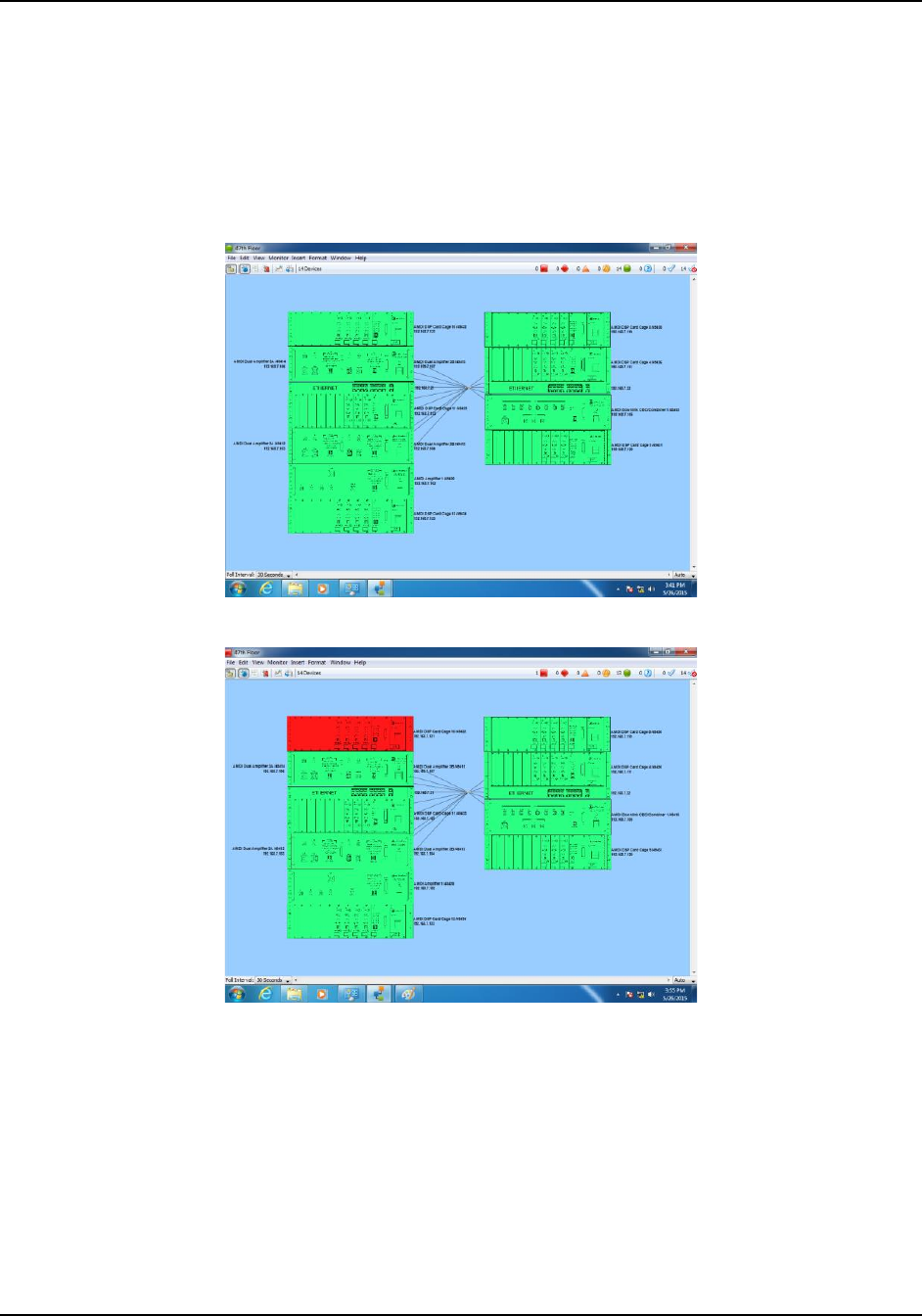
The Overview Map provides a high level view of the entire WTC system. Each icon on the Overview
Map represents an individual equipment room. The color of the icon, representing an equipment room,
indicates the most serious condition. If a failure condition is detected on any component in an equipment
room, the room’s icon will flash red.
Figure 1: NMS Overview Map
3.0 Maps
NMS User’s Manual Page 3-2
3.2 Node View Map
The Node View Map provides a detailed view of the equipment room which includes the Uplink and
Downlink racks. Devices in alarm mode flash red. The user can drill down into the device to view
detailed status of the hardware, set alarm thresholds, enable/disable the device, and update device
firmware.
Figure 2: Node View Map SYSTEM OK
Figure 3: Node View Map COMPONENT FAILED

4.0 Component Level GUI
NMS User’s Manual
4.0 COMPONENT LEVEL GUI
4.0 Component Level GUI
NMS User’s Manual Page 4-1
4.0 COMPONENT LEVEL GUI
By double clicking the component icon the user can view detailed status of the hardware, set alarm
thresholds, enable/disable the device, and update device firmware. Each component GUI includes 3 tab
pages Status, Thresholds, and Update.
4.1 AMDI DSP Processor Board Control
4.1.1 Status/Control
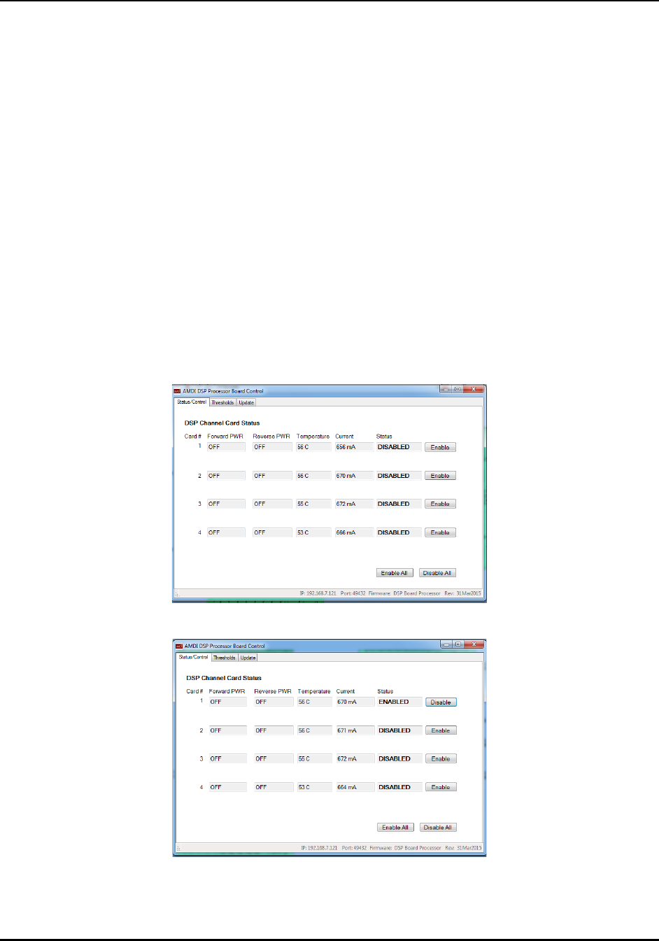
The status tab displays the current status for the individual DSP Channel Cards installed in the chassis.
The current measured Forward and Reverse power readings, in dBm, are displayed. If the
Forward/Reverse PWR readings display ‘OFF’ there is no signal present. The current board temperature
is displayed in degrees C. The instantaneous current draw is displayed in milliamps, mA. The Status
column displays the current board status which can be DISABLED, ENABLED, TEMP FAULT,
CURRENT FAULT, FORWARD PWR FUALT, REVERSE PWR FUALT, and COMMS Error.
Figure 4. DSP Status/Control tab
Figure 5. DSP Status/Control tab with channel Enabled.
To enable the RF output on a channel card click ‘Enable’.
4.0 Component Level GUI
NMS User’s Manual Page 4-2
To disable the RF output on an individual card click ‘Disable’.
To enable all cards in a Channel Card Cage click ‘Enable All’.
To disable all cards in a Channel Card Cage click ‘Disable All’.
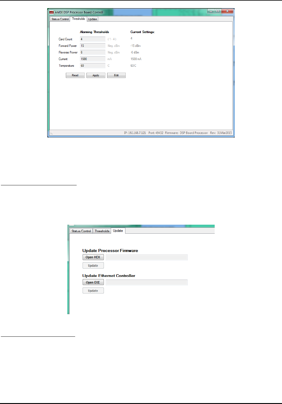
4.1.2 Thresholds
The Thresholds tab displays the alarm thresholds for the DSP Processor board. The below table outlines
each threshold:
Name
Description
Card Count
The number of DSP channel cards installed in the
corresponding card cage.
Forward Power
Number representing the minimum RF output
power value in – dBm.
Reverse Power
Number representing the maximum reflected
power reading in – dBm.
Current
Number representing the maximum allowable
current draw value in mA.
Temperature
Number representing the maximum allowable
temperature in degrees C.
Table 1. DSP Channel Card Threshold Values
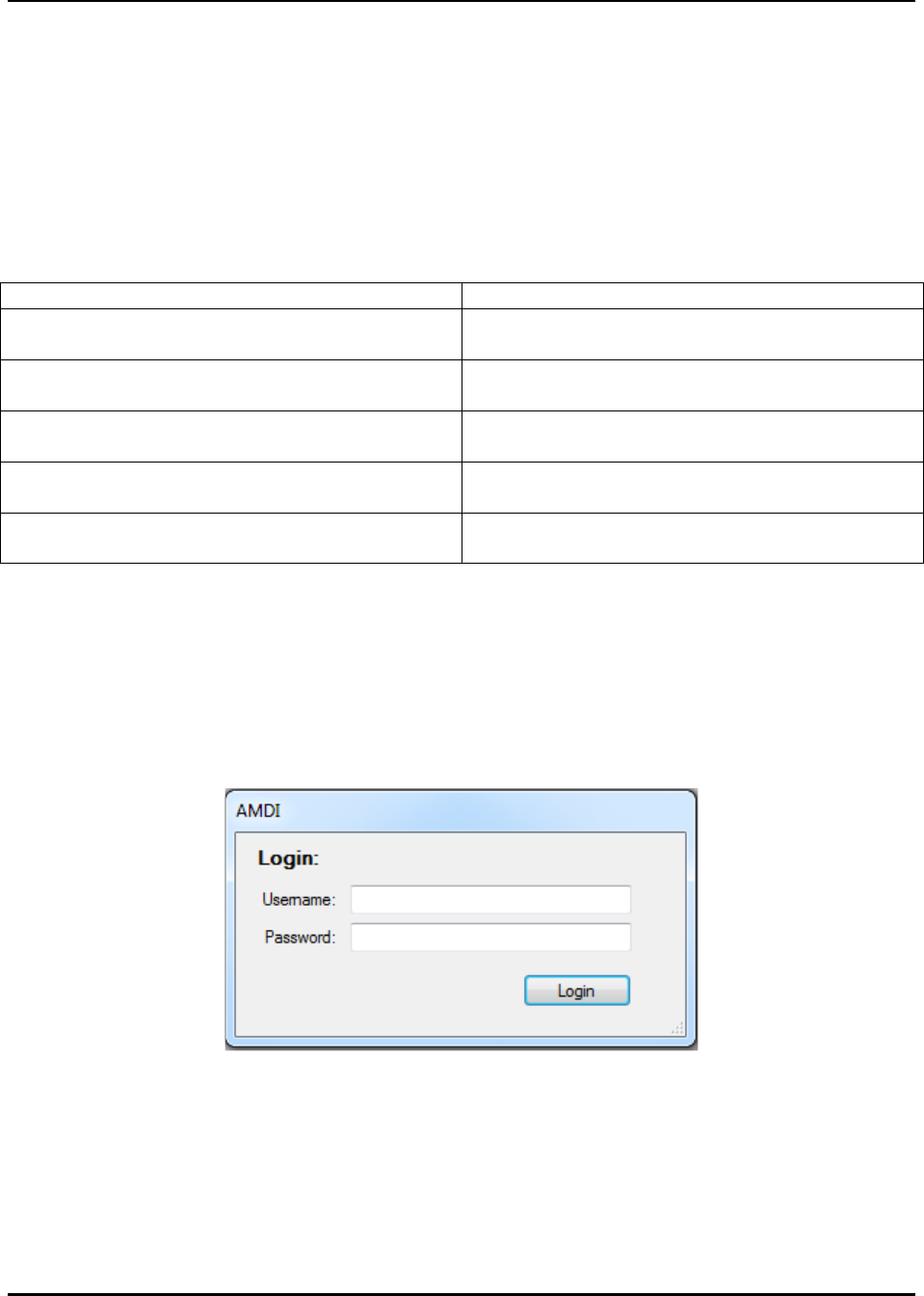
To edit thresholds, click the ‘Thresholds’ tab, then click ‘Edit’, when prompted for a username/password
use the following:
Username: AMDI
Password: admin
Figure 5. Login Prompt to edit thresholds
This will allow the user to make changes to the threshold values.
4.0 Component Level GUI
NMS User’s Manual Page 4-3
Figure 6. DSP Thresholds tab
4.1.3 Update
Update Processor Firmware:
To update the firmware running inside the processor, click ‘Open HEX’ and navigate to the
coorisponding .hex file. Once the file has been selected, click update. There will be a label that says
“Programming Complete” next to the Update button, and the button will be disabled.
Figure 7. DSP Channel Card Update Tab
Update Ethernet Controller:
To update the firmware running inside the Ethernet Interface, click ‘Open EXE’ and navigate to the
coorisponding .exe file. Once the file has been selected, click update. There will be a label that says
“Programming Complete” next to the Update button, and the button will be disabled.

4.0 Component Level GUI
NMS User’s Manual Page 4-4
4.1.4 Faults
The table below describes the different fault messages displayed in the Status column on the
‘Status/Control’ tab page. The alarms are generated whenever a measured value exceeds the threshold.
Fault Name
Description
Troubleshooting
TEMP FAULT
The temperature value is greater
that the threshold.
Verify fans are running.
Verify temperature threshold is
correct.
CURRENT FAULT
The current draw for the board is
greater than the current threshold
value.
Verify the board is connected
properly.
FORWARD POWER FAULT
The measured forward power
value is less than the forward
power threshold.
Verify DSP board RF output and
AGC settings using the AMDI UI
application.
REVERSE POWER FAULT
The measure reverse power value
is greater than the reverse power
threshold.
Verify RF cables are connected
properly.
COMMS ERROR
The number of detected channel
cards is less than the
programmed card count
threshold.
Verify the cards are properl y
seated in card cage.
Verify the threshold value
represents the number of channel
card present in the card cage.
Table 2. DSP Channel Cards Fault Messages
4.2 AMDI Power Amplifier Control
4.2.1 Status/Control
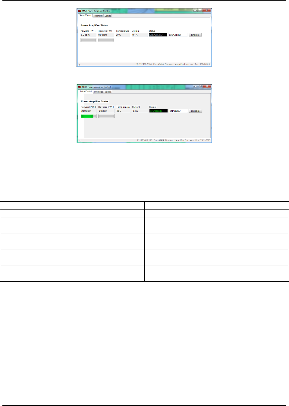
The status tab displays the current status for the power amplifier. The current measured Forward and
Reverse power readings, in dBm, are displayed. There are 2 progress bars that provide a visual
representation of the forward and reverse power. The current amplifier temperature is displayed in
degrees C. The instantaneous current draw is displayed in amps, A. The Status column displays the
current amplifier status which can be DISABLED, ENABLED, TEMP FAULT, CURRENT FAULT,
FORWARD PWR FUALT, and REVERSE PWR FUALT.
.
4.0 Component Level GUI
NMS User’s Manual Page 4-5
Figure 8. Power Amplifier Status/Control Tab disabled
Figure 9. Power Amplifier Status/Control Tab Enabled
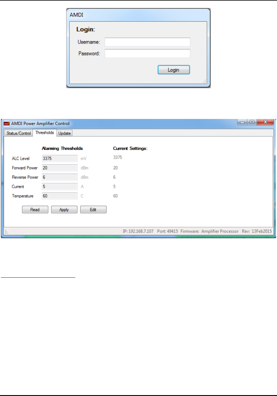
4.2.2 Thresholds
The Thresholds tab displays the alarm thresholds for power amplifier. The below table outlines each
threshold:
Name
Description
ALC
The value for Automatic Level Control
Forward Power
Number representing the minimum RF output
power value in dBm.
Reverse Power
Number representing the maximum reflected
power reading in dBm.
Current
Number representing the maximum allowable
current draw value in A.
Temperature
Number representing the maximum allowable
temperature in degrees C.
Table 3. Power Amplifier Threshold Values
To edit thresholds, click the ‘Thresholds’ tab, then click ‘Edit’, when prompted for a username/password
use the following:
Username: AMDI
Password: admin
4.0 Component Level GUI
NMS User’s Manual Page 4-6
Figure 10. Login Prompt to edit thresholds
This will allow the user to make changes to the threshold values.
Figure 11. Power Amplifier Thresholds Tab
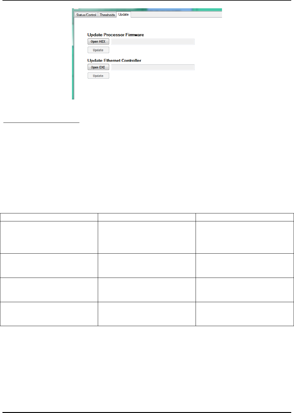
4.2.3 Update
Update Processor Firmware:
To update the firmware running inside the processor, click ‘Open HEX’ and navigate to the
coorisponding .hex file. Once the file has been selected, click update. There will be a label that says
“Programming Complete” next to the Update button, and the button will be disabled.
4.0 Component Level GUI
NMS User’s Manual Page 4-7
Figure 12 Power Amplifier Update Tab
Update Ethernet Controller:
To update the firmware running inside the Ethernet Interface, click ‘Open EXE’ and navigate to the
coorisponding .exe file. Once the file has been selected, click update. There will be a label that says
“Programming Complete” next to the Update button, and the button will be disabled.
4.2.4 Faults
The table below describes the different fault messages displayed in the Status column on the
‘Status/Control’ tab page. The alarms are generated whenever a measured value exceeds the threshold.
Fault Name
Description
Troubleshooting
TEMP FAULT
The temperature value is greater
that the threshold.
Verify fans are running.
Verify temperature threshold is
correct.
CURRENT FAULT
The current draw f or the
amplifier is greater than the
current threshold value.
Verify the amplifier is connected
and operating properly.
FORWARD POWER FAULT
The measured forward power
value is less than the forward
power threshold.
Verify the ALC threshold value
is configure properly.
REVERSE POWER FAULT
The measure reverse power value
is greater than the reverse power
threshold.
Verify RF cables are connected
properly.
Table 4. Power Amplifier Fault Messages
4.3 AMDI Cross Band Coupler
4.3.1 Status
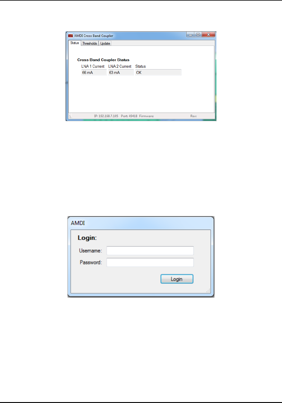
4.0 Component Level GUI
NMS User’s Manual Page 4-8
The status tab displays the current draw in millamps, mA, for the LNAs in the chassis. The status
column will display OK or CURRENT FAULT.
Figure 13 CBC Status tab
4.3.2 Thresholds
The thresholds tab allows the user to set the current draw threshold for the LNAs.
To edit thresholds, click the ‘Thresholds’ tab, then click ‘Edit’, when prompted for a username/password
use the following:
Username: AMDI
Password: admin
Figure 14 Login Prompt to edit thresholds
This will allow the user to make changes to the threshold values.
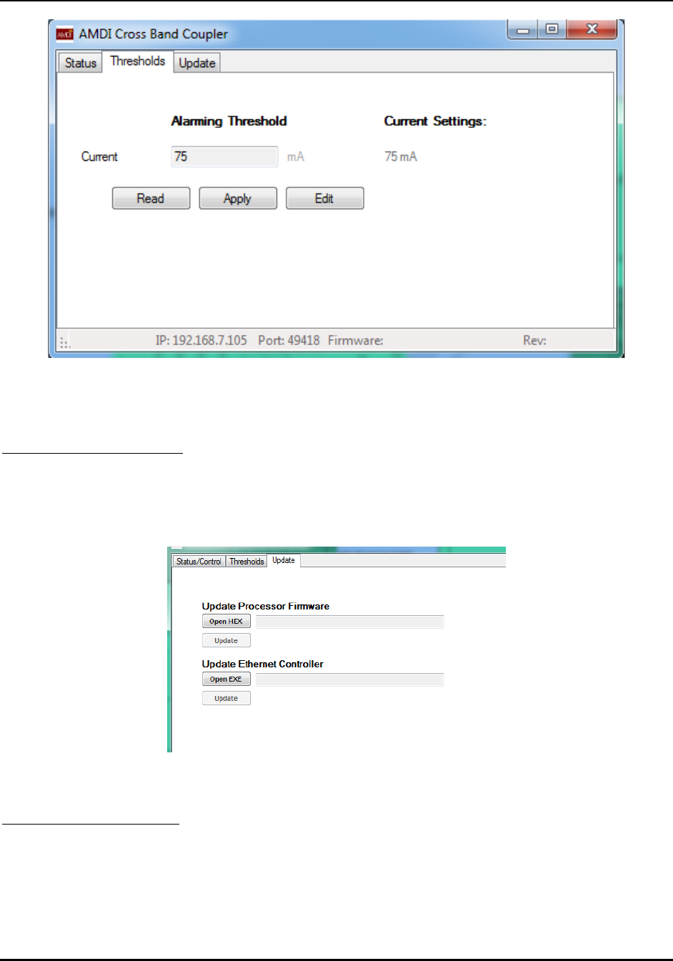
4.0 Component Level GUI
NMS User’s Manual Page 4-9
Figure 15 CBC Thresholds Tab
4.3.3 Update
Update Processor Firmware:
To update the firmware running inside the processor, click ‘Open HEX’ and navigate to the
coorisponding .hex file. Once the file has been selected, click update. There will be a label that says
“Programming Complete” next to the Update button, and the button will be disabled.
Figure 12 CBC Update Tab
Update Ethernet Controller:
To update the firmware running inside the Ethernet Interface, click ‘Open EXE’ and navigate to the
coorisponding .exe file. Once the file has been selected, click update. There will be a label that says
“Programming Complete” next to the Update button, and the button will be disabled.

4.0 Component Level GUI
NMS User’s Manual Page 4-10
4.3.4 Fault
The table below describes the fault message displayed in the Status column on the ‘Status’ tab page. The
alarm is generated whenever a measured value exceeds the threshold.
Fault Name
Description
Troubleshooting
CURRENT FAULT
The current draw for the LNA is
greater than the current threshold
value.
Verify the CBC is connected and
operating properly.
Table 5 CBC Fault Message
Back to Index
Appendix B
RACS (Radio Access Control System) Description
There are two equipment rooms in Tower-4, and each equipment room has an Uplink and Downlink
rack.
The Downlink Rack contains three DSP Card Cages, two Dual Amplifiers, one Single Amplifier, and
one CBC chassis. There are a total of eight processor boards in the Downlink rack; one board in
each Card Cage, two boards in each Dual Amplifier, and one board in the single amplifier. The CBC
chassis is passive and does not have a processor board.
The Uplink Rack contains three DSP Card Cages and one CBC chassis. There are a total of four
processor boards in the Uplink rack; one board in each Card Cage and one board in the CBC chassis.
Each processor board has an Ethernet interface and is connected to an Ethernet Switch in the
associated rack. Each processor board also has six relays that are the interface to the RACS system.
There are three wires associated with each relay; Common (COM), Normally Open (NO), and
Normally Closed (NC). There is a DB-25F connector on each front panel that brings out the eighteen
lines; three lines per each of the six relays.
A relay changes state from NO to NC if a corresponding fault is detected by the processor board. The
threshold for each fault function is programmable via the Graphic User Interface (GUI) program
provided with the system.
Five block diagrams are attached:
Figures 1 and 2 are high-level block diagrams showing the components of the system that implement
the RACS function for the DL and UL racks respectively. Each of the components described above is
listed along with the corresponding AMDI model number.
Figures 3, 4, and 5 show the RACS section of a typical Card Cage, DL Power Amplifier, and UL CBC
in more detail.
DSP Window Card RACS Interface
The Card Cage chassis has a backplane board that runs across the back of the chassis. The DSP
cards and the processor board plug into the backplane, which provides the signal path for an RS-422
interface between the processor board and each of the DSP Window cards.
The processor board sends command to, and receives status from, each of the DSP Window Cards.
Status messages from the Window card to the processor board include; Forward Power, Reflected
Power, Current, Temperature, Mode (narrow-band or broadband), and number of active channels.
Since there is one processor board per chassis, there is one set of six RACS relays per chassis. The
relays represent the composite status for the (three or four) DSP cards in the chassis. Any one of the
following faults on a channel card will result in the relay corresponding to that card changing state:
Forward Power Fault, Reflected Power Fault, Current Fault, Temperature Fault.
The following is a list of relay fault assignments:
DSP Channel Card #1 Fault
DSP Channel Card #2 Fault
DSP Channel Card #3 Fault
DSP Channel Card #4 Fault
Spare #1
Spare #2
Figure 3 shows the Card Cage block diagram and the RACS relay lines.
Power Amplifier RACS Interface
The Power Amplifier chassis contains either one or two power amplifier modules. A power amplifier
module consists of a power supply, power amplifier, optional combiner, and processor board.
Figure 4 shows the lines between the amplifier module and the processor board. Voltages
proportional to amplifier forward and reflected power are input to the processor board. ALC level,
ALC enable, and amplifier enable (key line, to turn the amplifier on and off) are output from the
processor board to the amplifier.
In addition to these signals, the processor board monitors amplifier current (via a sense resistor in
series with the power supply) and amplifier temperature (via a thermistor mounted to the amplifier
heat sink). A tachometer signal on the fan is monitored to ensure the fan is rotating.
The processor board sends command to, and receives status from, the amplifier and peripherals
(current, temperature, and fan status).
The following is a list of relay fault assignments:
Forward Power Fault
Reflected Power Fault
Over-Current Fault
Temperature Fault
Fan Fault
Spare
Uplink CBC RACS Interface
The Uplink CBC chassis contains a Cross-Band Coupler, two Splitters, and two LNA’s. There is one
processor board in the chassis that measures power supply current into each LNA.

The following is a list of relay fault assignments:
LNA #1 Over-Current Fault
LNA #2 Over-Current Fault
Spare #1
Spare #2
Spare #3
Spare #4
Notes:
1.RACS fault thresholds are the same as for the chassis front-panel LED’s. Thresholds are set using
the AMDI GUI.
2.The “Forward Power” fault is not defined at this time.
3.All faults are generated under firmware control of the processor board in the corresponding
chassis. These can be re-defined in later firmware versions.
Back to Index
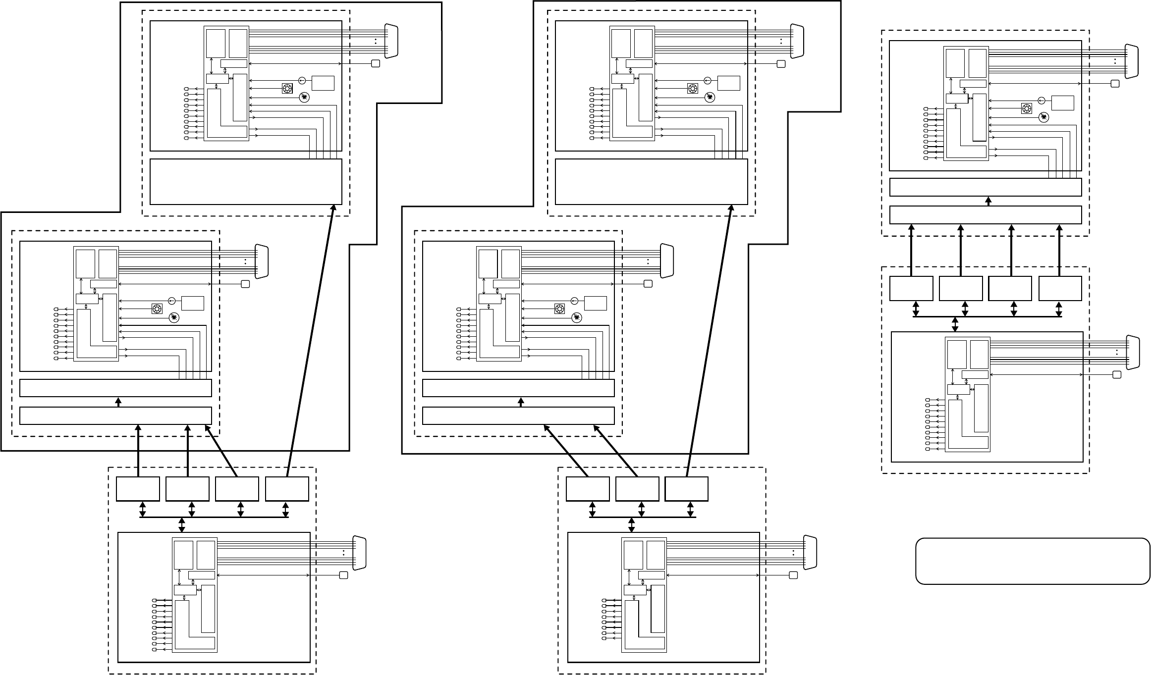
WTC4 HE Alarms Diagram
rev 3
Downlink Group
PROPRIETARY
This document is issued in strict confidence on condition that it is
not copied, reprinted, or disclosed to a third party, wholly or in part,
without written consent of Applied Micro Design, Incorporated.
Window
7
Window
9
Window
11
Window
12
Power Amplifier
Enable/Disable
Forward Pwr
Reverse Pwr
ALC
ALC Level
Power
Supply
Current Sense
Analog
Interface
Serial
Interface
Digital
Interface
Processor
Ethernet Interface
Status
Key
Fwd Pwr
Ref Pwr
Current
Current Fault
Temperature
Temp Fault
Fan Fault
Fan
RACS
NC
NC
NO
NO
NC
NC
NO
NO
Temperature
Fan Fault
T
Amplifier
Processor
Analog
Interface
Serial
Interface
Digital
Interface
Processor
Ethernet Interface
RACS
NC
NC
NO
NO
NC
NC
NO
NO
Power Amplifier
Enable/Disable
Forward Pwr
Reverse Pwr
ALC
ALC Level
Power
Supply
Current Sense
Analog
Interface
Serial
Interface
Digital
Interface
Processor
Ethernet Interface
Status
Key
Fwd Pwr
Ref Pwr
Current
Current Fault
Temperature
Temp Fault
Fan Fault
Fan
RACS
NC
NC
NO
NO
NC
NC
NO
NO
Temperature
Fan Fault
T
Amplifier
Processor
Power Amplifier
Enable/Disable
Forward Pwr
Reverse Pwr
ALC
ALC Level
Power
Supply
Current Sense
Analog
Interface
Serial
Interface
Digital
Interface
Processor
Ethernet Interface
Status
Key
Fwd Pwr
Ref Pwr
Current
Current Fault
Temperature
Temp Fault
Fan Fault
Fan
RACS
NC
NC
NO
NO
NC
NC
NO
NO
Temperature
Fan Fault
T
Amplifier
Processor
Window
1
Window
2
Window
3
Window
4
Analog
Interface
Serial
Interface
Digital
Interface
Processor
Ethernet Interface
RACS
NC
NC
NO
NO
NC
NC
NO
NO
Channel
Card
Processor
Window
8
Window
6
Window
10
Analog
Interface
Serial
Interface
Digital
Interface
Processor
Ethernet Interface
RACS
NC
NC
NO
NO
NC
NC
NO
NO
Channel
Card
Processor
Channel
Card
Processor
to Ethernet
switch
(MCAS)
DB-25
(RACS)
400 MHz Dual Amplifier
Model No. 1465PAD-3-1-400
400 MHz Dual Amplifier
Model No. 1465PAD-2-1-400
Channel Card Assembly
Model No. 1465DSP-4-2-P
Combiner
Channel Card Assembly
Model No. 1465DSP-4-2-P
Channel Card Assembly
Model No. 1465DSP-3-2-P
Power Amplifier
Combiner
Power Amplifier
Combiner
Channel Card Assembly
Model No. 1465DSP-4-2-P
DB-25
(RACS)
to Ethernet
switch
(MCAS)
DB-25
(RACS)
to Ethernet
switch
(MCAS)
to Ethernet
switch
(MCAS)
DB-25
(RACS)
to Ethernet
switch
(MCAS)
DB-25
(RACS)
DB-25
(RACS)
to Ethernet
switch
(MCAS)
DB-25
(RACS)
to Ethernet
switch
(MCAS)
800 MHz400 MHz400 MHz
Note: DB-25 connector has six (6) sets
of NO, NC and Common relay contacts.
DB-25
(RACS)
to Ethernet
switch
(MCAS)
Status
Power
W1
Fault
W2
Fault
W3
Fault
W4
Fault
Status
Power
W8
Fault
W6
Fault
W10
Fault
Status
Power
W7
Fault
W9
Fault
W11
Fault
W12
Fault
Figure 1
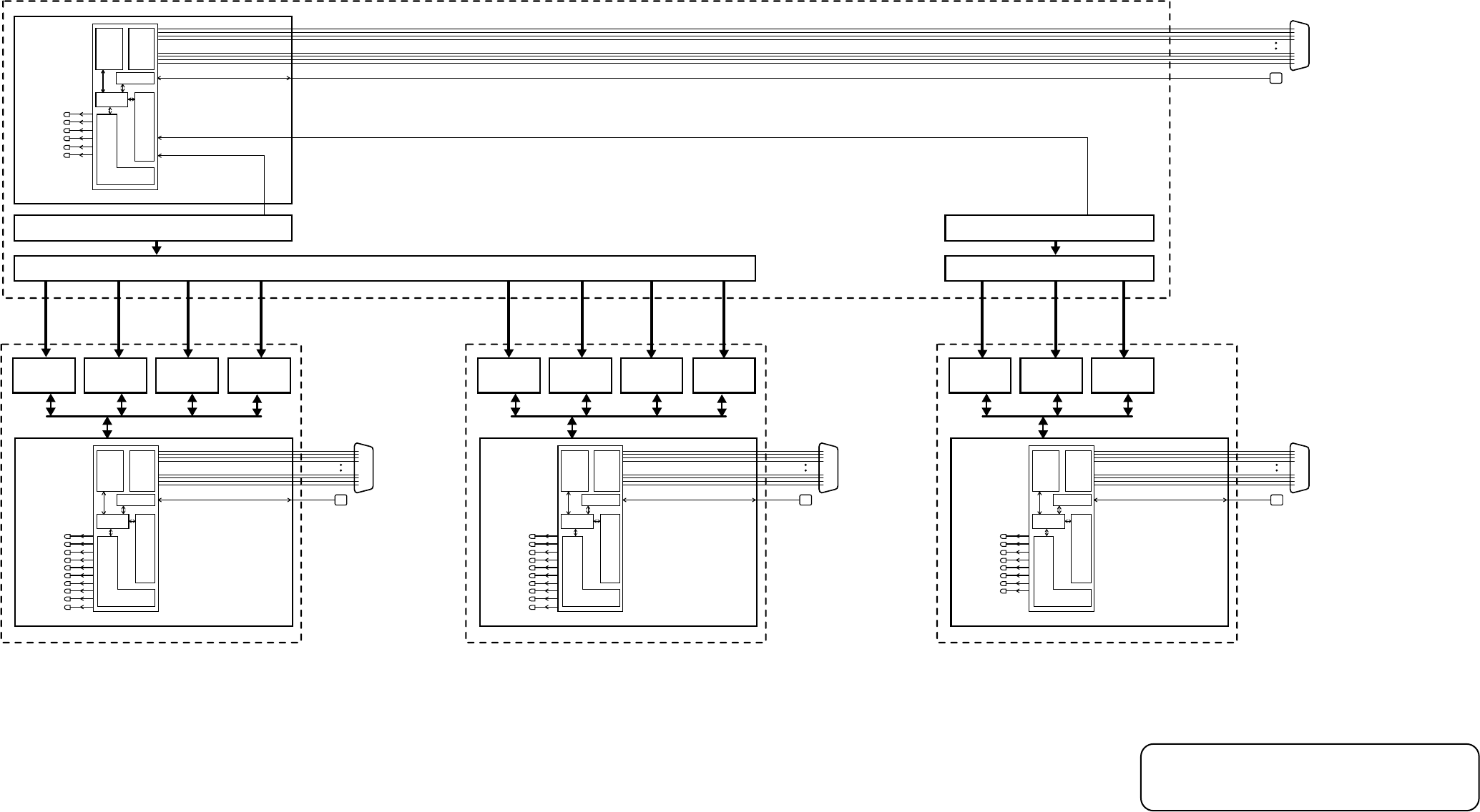
Uplink GroupWTC4 HE Alarms Diagram
rev 3
LNA
Analog
Interface
Serial
Interface
Digital
Interface
Processor
Ethernet Interface
Current
Current Fault
RACS
NC
NC
NO
NO
NC
NC
NO
NO
LNA
Processor
Window
1A
Window
1
Window
2
Window
3
Analog
Interface
Serial
Interface
Digital
Interface
Processor
Ethernet Interface
Status
RACS
NC
NC
NO
NO
NC
NC
NO
NO
Channel
Card
Processor
Splitter
DB-25
(RACS)
to Ethernet
switch
(MCAS)
to Ethernet
switch
(MCAS)
DB-25
(RACS)
Current Sense LNA 2
Current Sense LNA 1
LNA
Splitter
Window
4
Window
5
Window
7
Window
10
Analog
Interface
Serial
Interface
Digital
Interface
Processor
Ethernet Interface
RACS
NC
NC
NO
NO
NC
NC
NO
NO
Channel
Card
Processor
to Ethernet
switch
(MCAS)
DB-25
(RACS)
Window
8
Window
9
Window
11
Analog
Interface
Serial
Interface
Digital
Interface
Processor
Ethernet Interface
RACS
NC
NC
NO
NO
NC
NC
NO
NO
Channel
Card
Processor
to Ethernet
switch
(MCAS)
DB-25
(RACS)
800 MHz400 MHz
Channel Card Assembly
Model No. 1465DSP-4-2-P
Channel Card Assembly
Model No. 1465DSP-4-2-P
Channel Card Assembly
Model No. 1465DSP-3-2-P
400 MHz
PROPRIETARY
This document is issued in strict confidence on condition that it is
not copied, reprinted, or disclosed to a third party, wholly or in part,
without written consent of Applied Micro Design, Incorporated.
Note: DB-25 connector has six (6) sets
of NO, NC and Common relay contacts.
Status
Power
Power
W1A
Fault
W1
Fault
W2
Fault
W3
Fault
Status
Power
W4
Fault
W5
Fault
W7
Fault
W10
Fault
Status
Power
W8
Fault
W9
Fault
W11
Fault
Current
Current Fault
Figure 2
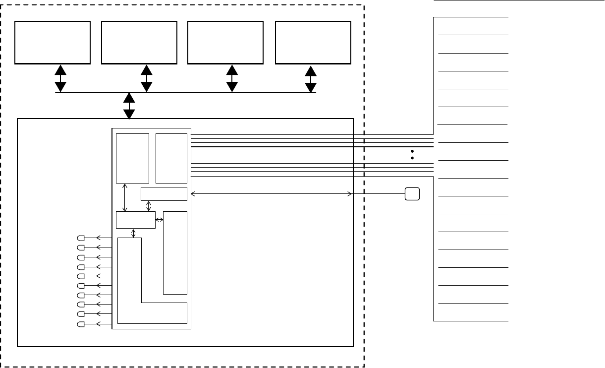
Figure 3
Window
1
Window
2
Window
3
Window
4
Analog
Interface
Serial
Interface
Digital
Interface
Processor
Ethernet Interface
RACS
Channel
Card
Processor
to Ethernet
switch
(MCAS)
DB-25
(RACS)
Status
Power
W1
Fault
W2
Fault
W3
Fault
W4
Fault
DSP Card # 1 NO
DSP Card # 1 COM
DSP Card # 1 NC
DSP Card # 2 NO
DSP Card # 2 COM
DSP Card # 2 NC
DSP Card # 3 NO
DSP Card # 3 COM
DSP Card # 3 NC
DSP Card # 4 NO
DSP Card # 4 COM
DSP Card # 4 NC
Spare # 1 NO
Spare # 1 COM
Spare # 1 NC
Spare # 2 NO
Spare # 2 COM
Spare # 2 NC
Alarm DB-25 Pin No.
1
3
2
5
7
6
9
11
10
14
16
15
18
20
19
22
24
23
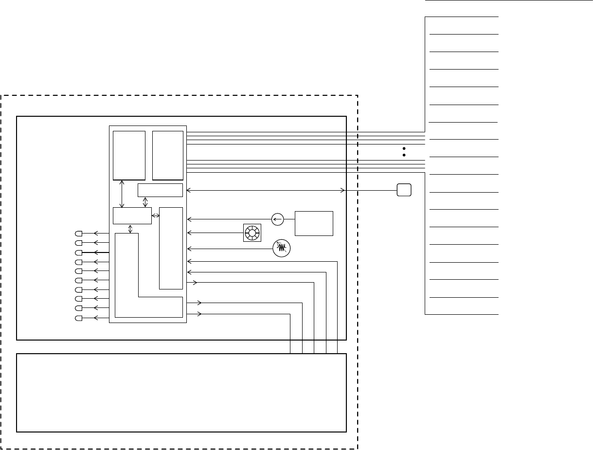
Figure 4
Power Amplifier
Enable/Disable
Forward Pwr
Reverse Pwr
ALC
ALC Level
Power
Supply
Current Sense
Analog
Interface
Serial
Interface
Digital
Interface
Processor
Ethernet Interface
Status
Key
Fwd Pwr
Ref Pwr
Current
Current Fault
Temperature
Temp Fault
Fan Fault
Fan
RACS
Temperature
Fan Fault
T
Amplifier
Processor
to Ethernet
switch
(MCAS)
DB-25
(RACS)
400 MHz
Fwd Pwr NO
Fwd Pwr COM
Fwd Pwr NC
Ref Pwr NO
Ref Pwr COM
Ref Pwr NC
Current Fault NO
Current Fault COM
Current Fault NC
Temp Fault NO
Temp Fault COM
Temp Fault NC
Fan Fault NO
Fan Fault COM
Fan Fault NC
Spare NO
Spare COM
Spare NC
Alarm DB-25 Pin No.
1
3
2
5
7
6
9
11
10
14
16
15
18
20
19
22
24
23
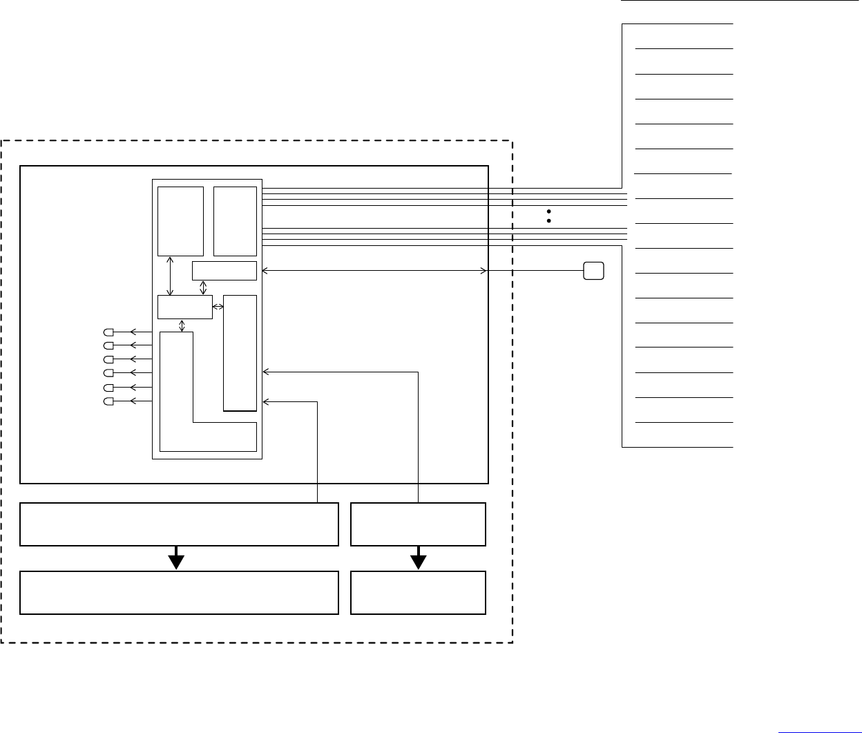
Figure 5
LNA
Analog
Interface
Serial
Interface
Digital
Interface
Processor
Ethernet Interface
Current
Current Fault
RACS
LNA
Processor
Splitter
DB-25
(RACS)
to Ethernet
switch
(MCAS)
Current Sense LNA 2
Current Sense LNA 1
LNA
Splitter
Status
Power
Current
Current Fault
LNA # 1 Current NO
LNA # 1 Current COM
LNA # 1 Current NC
LNA # 2 Current NO
LNA # 2 Current COM
LNA # 2 Current NC
Spare # 1 NO
Spare # 1 COM
Spare # 1 NC
Spare # 2 NO
Spare # 2 COM
Spare # 2 NC
Spare # 3 NO
Spare # 3 COM
Spare # 3 NC
Spare # 4 NO
Spare # 4 COM
Spare # 4 NC
Alarm DB-25 Pin No.
1
3
2
5
7
6
9
11
10
14
16
15
18
20
19
22
24
23
Back to Index
Appendix C
DSP User GUI Operation
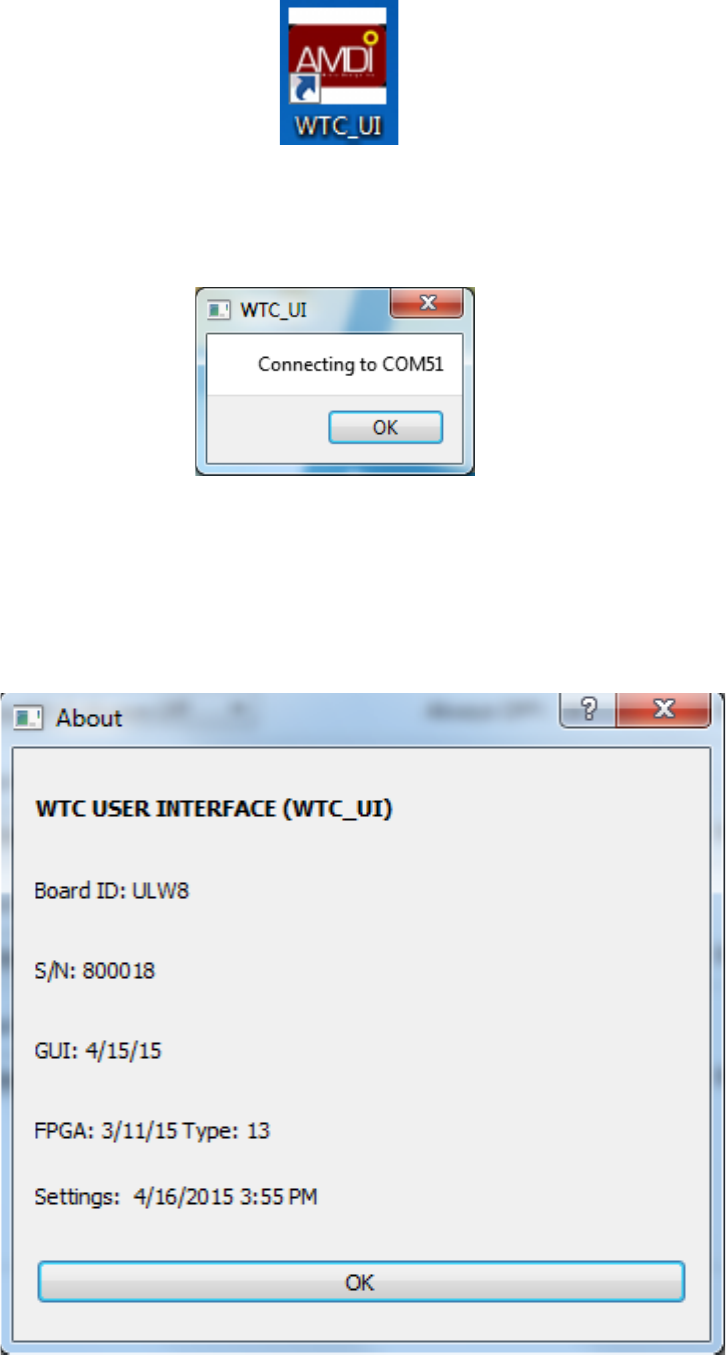
This document describes the operation of the WTC GUI, the graphical user interface program that is
used to configure each of the DSP modules. To use the WTC GUI connect a USB cable from the PC
to a DSP module and start the program by double-clicking on the desktop shortcut that looks like this:
When the WTC GUI program starts it looks for DSP modules on the USB interface. If it finds only one
module on the USB port, it displays a dialog box like the following one to announce on which USB
COM port it has found a DSP module on. Clicking the OK button dismisses the COM port dialog box.
On the other hand if it finds more than one the program lets the user select which module to work
with.
Next the WTC GUI program reads the current settings from the DSP module and also the module
board ID, serial number, and the revision dates of the GUI, firmware and settings. It displays that
information in an About dialog box like this:
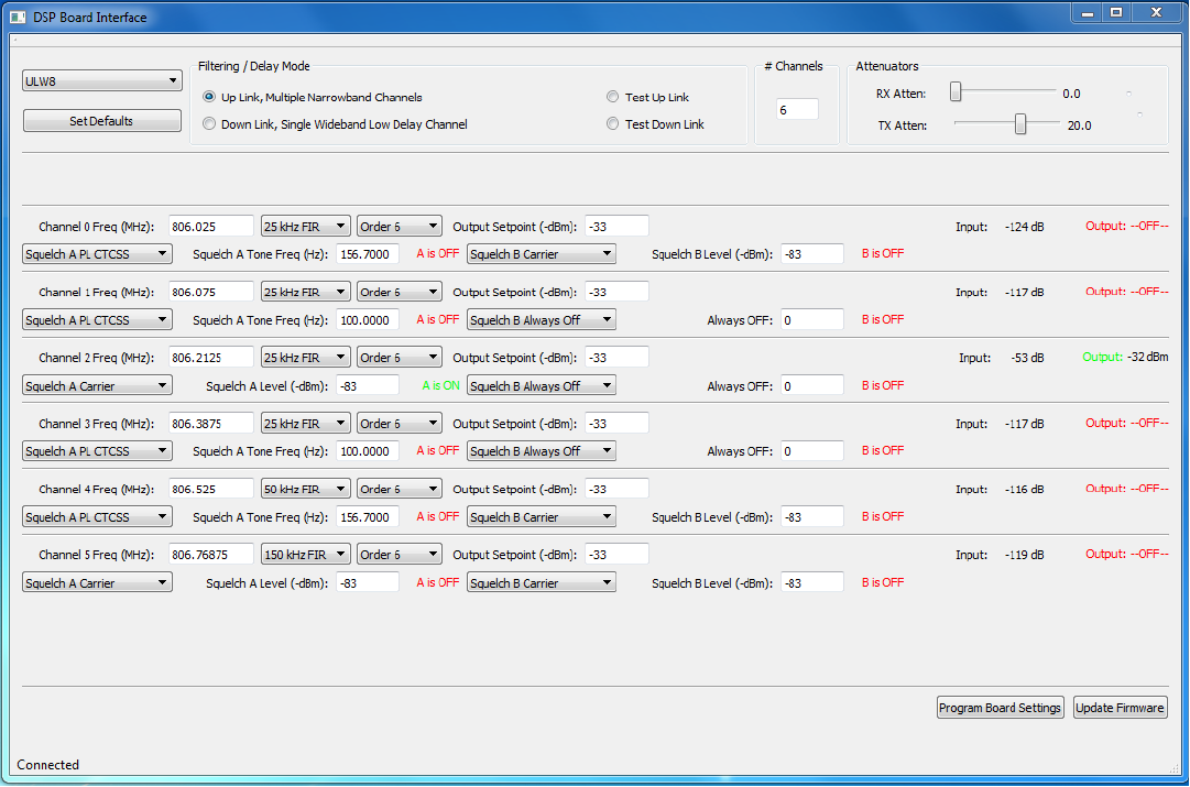
The About dialog, is displayed on top of the main GUI window. Here is an example of the Main
window for one of the WTC uplink modules, namely ULW8 (Up Link Window 8):
The settings that were read from the non-volatile memory on the DSP module allow the GUI program
to configure the GUI controls so they match the DSP module. The settings include the selected mode
which may be either “single channel low delay mode” which is normally used for the downlink or
“multiple channel narrowband mode” which is usually used for uplink.
The WTC firmware allows up to eight channels in uplink mode but other firmware is available from
AMDI that allows up to sixteen channels per DSP module. The ULW8 has six channels.
The GUI hides the GUI controls for the channels beyond those six since the settings read from the
board tell the GUI program that for the “Up Link Window 8” module only six channels are used. To use
a different number of channels the user only needs to change the number in the edit box labeled “# of
Channels”.
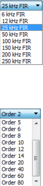
As you can see in the figure above, for each channel the GUI provides controls that specify these
values:
Channel Frequency (MHz)
Channel filter bandwidth
Channel filter order
Output AGC setpoint (dBm)
Squelch A and B types
Squelch A and B values
The GUI also provides the following outputs:
Squelch A and B ON or OFF indicators
Channel Input signal level (dBm)
Channel Output signal level (dBm)
Here is an explanation of some of these settings. Each channel uses Digital Signal Processing to
implement very flexible filters. The user can control both the filter bandwidth and the filter sharpness
and time delay. The filter bandwidth is selected using this control:
The filter sharpness and time delay are related. Sharper filters have a longer time delay. Time delay is
important in applications in which a receiver may receive both the signal that has passed through the
re-broadcast equipment and the signal directly from the transmitter. The following control lets the user
select the filter order which is a measure of the filter’s sharpness. For each channel this control lets
the user select the filter order:
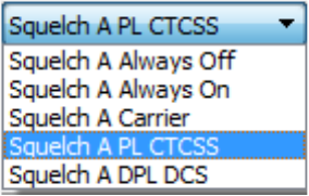
A filter with an order of 6 provides an input to output delay of about 24 microseconds but the filter
transitions from its passband to its stop bands slowly. A filter with an order of 80, on the other hand
has sharp edges but a longer delay.
Each channel has two squelch circuits because in some applications two different services share the
same frequency channel. In other cases more than one service are so close in frequency that a single
re-broadcast channel is used to handle both. For both Squelch A and Squelch B the user can select
using one of the two “Squelch Type” controls like these:
As the user changes the “Squelch Type” the prompt for the “Squelch Value” edit box changes. For
Carrier squelch type it reads “Squelch A Level (dBm):” as shown for ULW8 channel 2. For “PL
CTCSS” squelch type it reads “Squelch A Tone Freq (Hz):” as shown for ULW8 channel 0. For “DPL
DCS” squelch type the prompt is “Squelch A DPL Code:”
Notice, in the ULW8 figure above, that for channel 2 there is green text that reads “A is ON” and red
text that reads “B is OFF”. That text lets the user see the current output of each of the channel’s two
squelch circuits. When either Squelch A or Squelch B is ON then the channel is keyed on. When it is
keyed on the output level text for the channel indicates the output level in dBm.
The input level text for each channel shows the level of the signal that has passed through the
channel’s filter. The ULW8 screen capture was done while there was a signal within that channel at
about -53 dBm.
The edit box just to the right of the “Output Setpoint (-dBm):” text lets the user specify the desired
output signal level (at the DSP module’s output) for each channel that is “Keyed ON” by the squelch
circuits.
The description so far has been focused on “Up Link, Multiple Narrowband Channels” mode. In that
mode the time delay is less critical. The signal path is from the portable radio in the building to the
distributed antennas through the DSP modules, combiners and amplifiers through fiber optic links to
the communication HUB. So there is very little chance that the receiver located distant from the
portable at the hub will receive both the signal directly from the portable and through the channelized
re-broadcast system. In this case the filters can be selective so they pass only one or two radio
channels each even though this higher selectivity comes at the price of increased time delay. The
filter order control described above lets the user trade off filter selectivity for time delay for each
channel.
For downlink the signal path is from transmitters at the communication hub is via fiber optic cables
through the DSP modules to 5 watt amplifiers to transmit on the distributed antenna system that runs
up both stairwells. Since some of that transmitted signal and a signal directly from the transmitter may
be received by a portable radio inside or near the building, the time delay for the downlink is more
critical. The DSP module provides “Down Link, Single Wideband Low Delay Channel” mode to
achieve a delay less than 10 microseconds for this case. The screen shot that follows shows a typical
module in this mode. Many of the GUI controls are the same as those described above. The following
screen shot shows a typical Down Link module in this case Down Link Window 11 (DLW11).
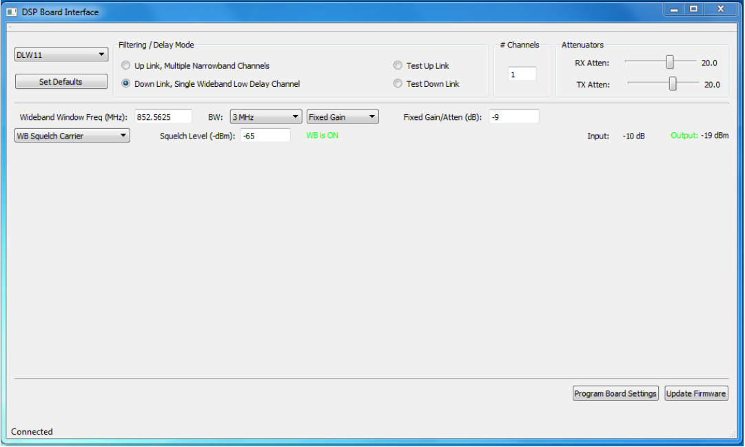
Notice that the BW: is set to 3 MHz. The BW control lets the user select from 50kHz, 100 kHz, 150
kHz, 200 kHz, 250 kHz, 500 kHz, 1 MHz, 1.5 MHz, 2 MHz, 2.5 MHz, 3 MHz, 3.5 MHz, 4 MHz, 5 MHz
or 5.5 MHz. There are two gain modes available Fixed Gain and AGC. In fixed gain mode there is an
edit box labeled “Fixed Gain/Atten (dB):”. In the case shown above the fixed gain is set to -9 dB. For
downlink the signals are relatively strong. They arrive from the communication hub via the fiber at a
level of -10 dBm. For DLW11 the signal will pass through a 4:1 combiner and then a 5 watt amplifier
to the Distributed antenna system. The value of -9 dB has been chosen to make the level at the DAS
after the loss in the combiner and the gain of the amplifier the specified level. Some down link module
outputs pass through either no combiners or combiners with different losses so the values in the fixed
gain box vary to compensate for the signal path.
If AGC mode had been chosen then the prompt text would read “Output Setpoint (-dBm):” and the
DSP circuitry would adjust the gain to make the output equal to the value in the edit box. The WB
Squelch choices are WB Squelch Always OFF, WB Squelch Always ON and WB Squelch Carrier. The
latter is the usual choice with the others used mostly for testing. There is red or green text that
indicates whether the squelch is off or on. As you can see there is also a measure of the input and
output signal level displayed.
Notice the slider control labeled RX Attenuator in the upper right corner of the screen. For the
downlink mode it is set to 20 dB of attenuation. That is because the input is relatively strong at -10
dBm. For the uplink mode the signals may be quite weak, as low as -83 dBm, when they arrive at the
DSP module so for uplink the RX attenuator is set to 0 dB of attenuation.
At the bottom of the GUI are two pushbuttons. The “Program Board Settings” pushbutton causes the
changes currently on the GUI controls to be saved to the DSP module’s non-volatile memory. The
settings are loaded into the Digital Signal Processing hardware when the power to the module is
turned on.

The pushbutton labeled “Update Firmware” is used to write new firmware into the DSP module. It lets
the user select a “.BIT” file to load. This should only be done when AMDI sends a new firmware file
and the new file has been loaded onto the PC. The present firmware file is on the PC named
AmdiDspWtc.bit.
19516 Amaranth Drive Germantown MD 20874
ph 301.540.9506
info@appliedmicrodesign.com
www.appliedmicrodesign.com
Applied Micro Design Inc.
Back to Index