Balluff BISL409 BIS L-40X Series 4 User Manual 1 of 2
Balluff Inc BIS L-40X Series 4 1 of 2
UserManual.wiki
>
Balluff
>
BISL409 User Manual
>
User Manual 1 of 2.pdf
Contents
1.
User Manual 1 of 2.pdf
2.
User Manual 2 of 2.pdf
User Manual 1 of 2.pdf
Navigation menu
Upload a User Manual
Namespaces
Wiki Guide
HTML
PDF
Info
Views
User Manual
Discussion / Help
Navigation

![16 BIS L-409-045-001-07-S4DimensionsCharacteristic dataMechanical dataTechnical Data5A41Fig. 10: Dimensions for BIS L-409-045-001-07-S4 processor [mm]A Clear zone BIS L-409-045-001-07-S4Characteristic data when used with data carriers (installed in clear zone)When v = 0 (static)Distance [mm] readOffset from center axis at distance: [mm]0 - 20 0 - 35 0 - 45 0 - 15BIS L-200-03 / BIS L-100-05 25 15 – – –BIS L-201-03 / BIS L-101-05 35 – 20 – –BIS L-202-03 / BIS L-102-05 48 – – 25 –BIS L-203-03 / BIS L-103-05 16 – – – 10Housing material Plastic (PBT)Wiring Connector, M12 4-pin, A-codedEnclosure rating IP65 (with connectors)Weight 220 gBIS L-409 IO-Link DeviceProcessor](https://usermanual.wiki/Balluff/BISL409.User-Manual-1-of-2-pdf/User-Guide-2864613-Page-16.png)
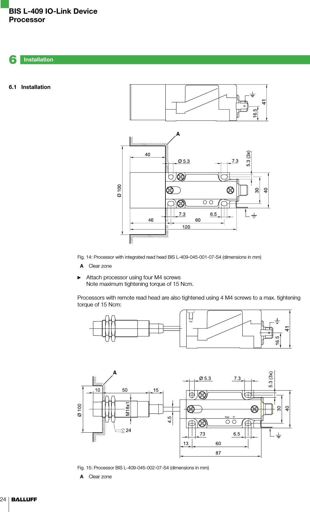
![18A41Fig. 11: Dimensions for BIS L-409-045-002-07-S4 processor [mm]A Clear zone BIS L-409-045-002-07-S4Characteristic data when used with data carriers (installed in clear zone)When v = 0 (static)Distance [mm] readOffset from center axis at distance: [mm]0 - 10 0 - 15 0 - 20BIS L-200-03 / BIS L-100-05 15 10 – –BIS L-201-03 / BIS L-101-05 18 12 12 –BIS L-203-03 / BIS L-103-05 10 4 – –Housing material Plastic (PBT)Read head housing material CuZn nickel platedWiring Connector, M12 4-pin, A-codedEnclosure rating IP67Weight 200 g BIS L-409-045-002-07-S4DimensionsCharacteristic dataMechanical dataTechnical data5BIS L-409 IO-Link DeviceProcessor](https://usermanual.wiki/Balluff/BISL409.User-Manual-1-of-2-pdf/User-Guide-2864613-Page-18.png)
![20A41Fig. 12: Dimensions for BIS L-409-045-003-07-S4 processor [mm]A Clear zone BIS L-409-045-003-07-S4Characteristic data when used with data carriers (installed in clear zone)When v = 0 (static)Distance [mm] readOffset from center axis at distance: [mm]0 - 5 0 - 8 0 - 11BIS L-203-03 / BIS L-103-05 7 4 – –Housing material Plastic (PBT)Read head housing material*) CuZn nickel platedWiring Connector, M12 4-pin, A-codedEnclosure rating IP67Weight 170 g BIS L-409-045-003-07-S4DimensionsCharacteristic dataMechanical dataTechnical data5BIS L-409 IO-Link DeviceProcessor](https://usermanual.wiki/Balluff/BISL409.User-Manual-1-of-2-pdf/User-Guide-2864613-Page-20.png)
![22 BIS L-409-045-004-07-S4DimensionsCharacteristic dataMechanical dataAA41Fig. 13: Dimensions for BIS L-409-045-004-07-S4 processor [mm]A Clear zone BIS L-409-045-004-07-S4Characteristic data when used with data carriers (installed in clear zone)When v = 0 (static)Distance [mm] readOffset from center axis at distance: [mm]0 - 10 0 - 15 0 - 20BIS L-200-03 / BIS L-100-05 15 10 – –BIS L-201-03 / BIS L-101-05 18 12 12 –BIS L-203-03 / BIS L-103-05 10 4 – –Housing material Plastic (PBT)Read head housing material CuZn nickel platedWiring Connector, M12 4-pin, A-codedEnclosure rating IP67Weight 170 gTechnical data5BIS L-409 IO-Link DeviceProcessor](https://usermanual.wiki/Balluff/BISL409.User-Manual-1-of-2-pdf/User-Guide-2864613-Page-22.png)

![www.balluff.com 359.1 Project administrationGSD fileHead moduleData modules9.2 Integration into project administration software9.3 Integration exampleInstalling the GSD fileIn project administration of fieldbus devices, a physical device is mapped as a modular system consisting of a head module and multiple data modules. The device data required for project planning are stored in GSD files (Generic Station Description). The GSD files are made available by the vendors of the IO-Link Masters. The GSD files for Balluff IO-Link Masters are available on the Internet at “www.balluff.com/software”for downloading.The data modules for an IO-Link device are shown in the project administration software by port. The GSD file provides the possible data modules (inputs or outputs of various data width). For configuring the IO-Link device the appropriate data modules are assigned to a particular port.First the head module is inserted into the configuration. The head module is coded according to the special identification format. head modules in this coding are used for identification and parameter setting and have a data width of 2 bytes input of 2 bytes input/output data.The data modules are arranged onto the head module in order of the slots for ports/PINs. To integrate a BIS L-409 IO-Link device the following steps a generally required:Load the GSD file for the IO-Link Master into the hardware configuration of the host system.Insert the data module “Input 8 bytes/Output 8 bytes” (IOL_I/O_8/8_Byte) for the used IO-Link port (Port X, Pin 4).This assigns the start addresses of the input and output data. The input and output data can, as described in Section 10, be used for operating the BIS L-409-....Integration of a BIS L-409-IO-Link-Device is shown using the example of a BNI-PBS-IO-Link-Master. In the example a Siemens S7 with “SIMATIC-MANAGER” program and project adminis-tration software is used. The exact procedure will vary from case to case depending on the software used and may differ from this example. To do the project planning on the PC, the GSD file for the module must be installed:Open new or existing project.Open hardware configurator.Select menu command “Tools| Install new GSD...”.The “Install new GSD” window opens.Select directory and GSD file.The [Install] button only becomes active if a GSD file is selected.Click on [Install].The GSD file is installed.Once the operation is finished, a message appears.Confirm the message and close the window.Select menu command “Tools | Update catalog”.The modules are displayed in the project tree.1.2.⇒►►►⇒►⇒►⇒⇒►►⇒Startup9BIS L-409 IO-Link DeviceProcessor](https://usermanual.wiki/Balluff/BISL409.User-Manual-1-of-2-pdf/User-Guide-2864613-Page-35.png)
![50Decimal Hex Control CodeASCII Decimal Hex ASCII Decimal Hex ASCII0 00 Ctrl @ NUL 43 2B + 86 56 V1 01 Ctrl A SOH 44 2C , 87 57 W2 02 Ctrl B STX 45 2D - 88 58 X3 03 Ctrl C ETX 46 2E . 89 59 Y4 04 Ctrl D EOT 47 2F / 90 5 A Z5 05 Ctrl E ENQ 48 30 0 91 5B [6 06 Ctrl F ACK 49 31 1 92 5C \7 07 Ctrl G BEL 50 32 2 93 5D [8 08 Ctrl H BS 51 33 3 94 5E ^9 09 Ctrl I HT 52 34 4 95 5F _10 0 A Ctrl J LF 53 35 5 96 60 `11 0B Ctrl K VT 54 36 6 97 61 A12 0C Ctrl L FF 55 37 7 98 62 B13 0D Ctrl M CR 56 38 8 99 63 c14 0E Ctrl N SO 57 39 9 100 64 d15 0F Ctrl O SI 58 3 A : 101 65 e16 10 Ctrl P DLE 59 3B ; 102 66 f17 11 Ctrl Q DC1 60 3C < 103 67 g18 12 Ctrl R DC2 61 3D = 104 68 h19 13 Ctrl S DC3 62 3E > 105 69 i20 14 Ctrl T DC4 63 3F ? 106 6 A j21 15 Ctrl U NAK 64 40 @ 107 6B k22 16 Ctrl V SYN 65 41 A 108 6C L23 17 Ctrl W ETB 66 42 B 109 6D m24 18 Ctrl X CAN 67 43 C 110 6E n25 19 Ctrl Y EM 68 44 D 111 6F o26 1 A Ctrl Z SUB 69 45 E 112 70 p27 1B Ctrl [ ESC 70 46 F 113 71 q28 1C Ctrl \ FS 71 47 G 114 72 r29 1D Ctrl ] GS 72 48 H 115 73 s30 1E Ctrl ^ RS 73 49 I 116 74 t31 1F Ctrl _ US 74 4 A J 117 75 u32 20 SP 75 4B K 118 76 V33 21 ! 76 4C L 119 77 W34 22 " 77 4D M 120 78 X35 23 # 78 4E N 121 79 Y36 24 $ 79 4F O 122 7 A Z37 25 % 80 50 P 123 7B {38 26 & 81 51 Q 124 7C |39 27 ‘ 82 52 R 125 7D }40 28 ( 83 53 S 126 7E ~41 29 ) 84 54 T 127 7F DEL42 2 A * 85 55 U ASCII tableAppendixBIS L-409 IO-Link DeviceProcessor](https://usermanual.wiki/Balluff/BISL409.User-Manual-1-of-2-pdf/User-Guide-2864613-Page-50.png)