Balluff BISL409 BIS L-40X Series 4 User Manual 1 of 2
Balluff Inc BIS L-40X Series 4 1 of 2
Balluff >
Contents
- 1. User Manual 1 of 2.pdf
- 2. User Manual 2 of 2.pdf
User Manual 1 of 2.pdf

Technical Description, User's Guide
English
BIS L-409-045-00x-07-S4
A
41
www.balluff.com

www.balluff.com 3
8
7
6
5
4
3
2
1
BIS L-409 IO-Link Device
Processor
Notes to the user 5
1.1 About this manual 5
1.2 Structure of the manual 5
1.3 Typographical conventions 5
1.4 Symbols 5
1.5 Abbreviations 6
Safety 7
2.1 Intended use 7
2.2 General safety notes 7
2.3 Meaning of the warnings 7
Getting Started 8
3.1 Mechanical connection 8
3.2 Electrical connection 11
Basic knowledge 13
4.1 Function principle of Identification Systems 13
4.2 System topology 14
4.3 Read distance/offset 15
4.4 Product description 15
4.5 Data security 15
4.6 IO-Link basic knowledge 15
Technical Data 16
BIS L-409-045-001-07-S4 16
BIS L-409-045-002-07-S4 18
BIS L-409-045-003-07-S4 20
BIS L-409-045-004-07-S4 22
Installation 24
6.1 Installation 24
6.2 Electrical connection 27
6.3 Hardware settings 28
IO-Link Basics 29
7.1 Digital point-to-point connection 29
7.2 Process data container 30
7.3 Direct parameter page 30
Setting the processor parameters 32
8.1 Required data 32
8.2 Parameterization data mapping 33

4
9
10
BIS L-409 IO-Link Device
Processor
Startup 35
9.1 Project administration 35
9.2 Integration into project administration software 35
9.3 Integration example 35
Device Function 41
10.1 Function principle 41
10.2 Operating mode 41
10.3 Process data 42
10.4 Protocol sequence 44
10.5 Protocol examples 44
10.6 Error codes 46
10.7 Data transmission timing 47
Appendix 49
Ordering code 49
Accessories 49
ASCII table 50

www.balluff.com 5
This manual describes processors in the series BIS L-409-... identification system as well as
startup instructions for immediate operation.
The manual is organized so that the sections build on one another.
Section 2: Basic safety information.
Section 3: The main steps for installing the identification system.
Section 4: Introduction to the material.
Section 5: Technical data for the processor.
Section 6: Mechanical and electrical connection.
Section 7: Basics for the IO-Link communications standard.
Section 8: User-defined processor settings.
Section 9: Integration into a fieldbus system using Profibus as an example.
Section 10: Processor and host system interaction.
The following conventions are used in this manual.
Enumerations are shown in list form with bullet points.
Entry 1,
Entry 2.
Action instructions are indicated by a preceding triangle. The result of an action is indicated by
an arrow.
Action instruction 1.
Action result.
Action instruction 2.
Numbers:
Decimal numbers are shown without additional indicators (e.g. 123),
Hexadecimal numbers are shown with the additional indicator hex (e.g. 00hex).
Parameters:
Parameters are shown in italics (e.g. CRC_16).
Directory paths:
References to paths in which data are stored or are to be saved to are shown in small caps (e.g.
Project:\Data tyPes\User DefineD).
Cross-references indicate where additional information on the topic can be found (see “Technical
data” starting page 16).
Attention!
This symbol indicates a security notice which most be observed.
Note, tip
This symbol indicates general notes.
–
–
►
⇒
►
–
–
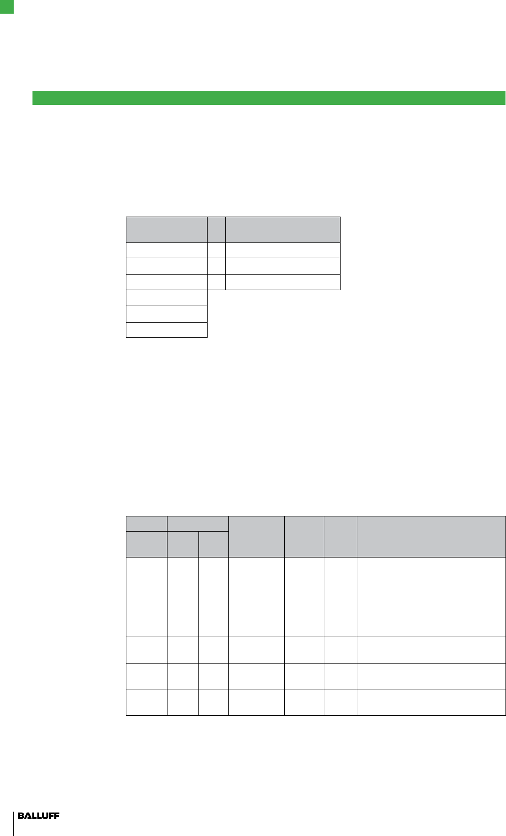
1.1 About this
manual
1.2 Structure of the
manual
1.3 Typographical
conventions
Enumerations
Actions
Syntax
Cross-references
1.4 Symbols
Notes to the user
1
BIS L-409 IO-Link Device
Processor

6
BIS Balluff Identification System
CRC Cyclic Redundancy Code
DPP Direct Parameter Page
EMC Electromagnetic Compatibility
LSB Least Significant Bit
MSB Most Significant Bit
PC Personal Computer
SIO Standard IO
SPDU Service Protocol Data Unit
PLC Programmable Logic Controller
TCP Transmission Control Protocol
1.5 Abbreviations
Notes to the user
1
BIS L-409 IO-Link Device
Processor
www.balluff.com 7
BIS L-409-... processors together with the other components of the BIS L system comprise the
identification system.
They may be used only for this purpose in an industrial environment corresponding to Class A of
the EMC Law.
This description applies to the compact processors in the BIS L-409-... series.
Installation and startup
Installation and startup are to be performed only by trained specialists. Any damage resulting
from unauthorized manipulation or improper use voids the manufacturer's guarantee and war-
ranty.
When connecting the processor to an external controller, observe proper selection and polarity of
the connection as well as the power supply (see “Installation” on page 24).
The processor must be powered only using approved power supplies (see “Technical data”
starting on page 16).
Attention!
This is a Class A device. This device may cause RF disturbances in residential areas;
in such a case the operator may be required to take appropriate countermeasures.
Operation and testing
The operator is responsible for observing local prevailing safety regulations.
When defects and non-clearable faults in the Identification System occur, take it out of service
and secure against unauthorized use.
Attention!
The pictogram used with the word “Caution” warns of a possible hazardous situation
affecting the health of persons or equipment damage. Ignoring these warnings can
result in injury or equipment damage.
Always observe the described measures for preventing this danger.►
2.1 Intended use
2.2 General safety
notes
2.3 Meaning of the
warnings
Safety
2
BIS L-409 IO-Link Device
Processor
8
3.1 Mechanical
connection
Getting Started
3
A
41
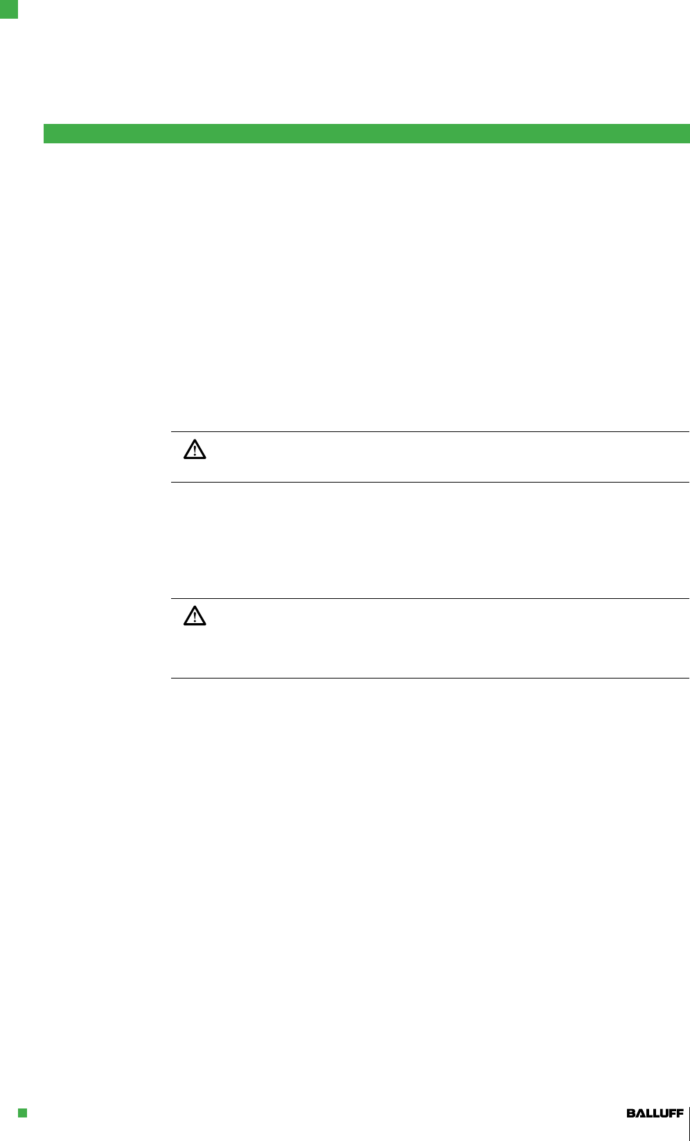
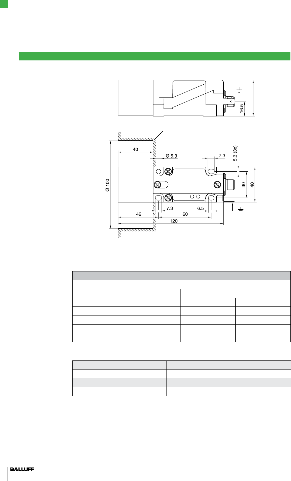
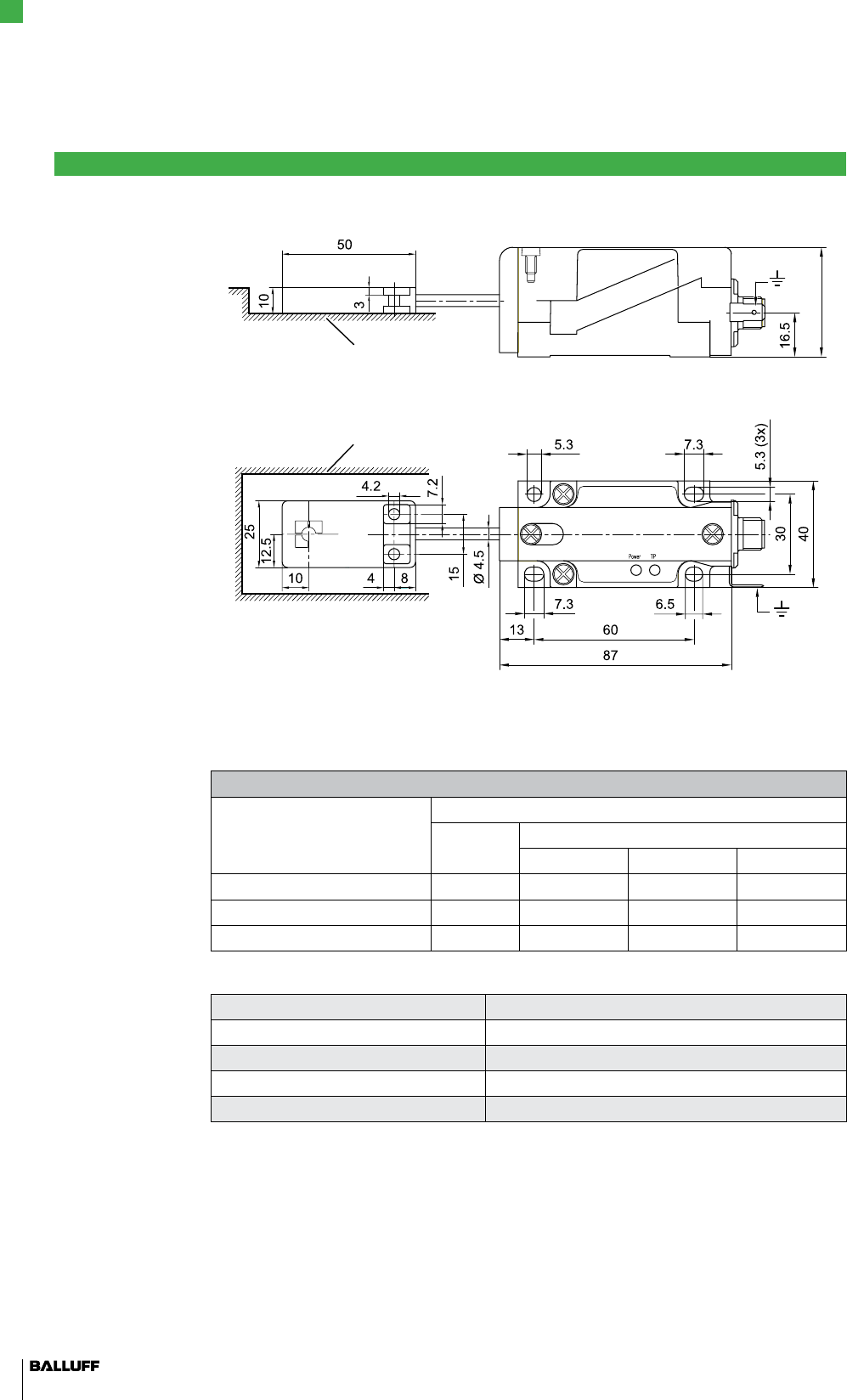
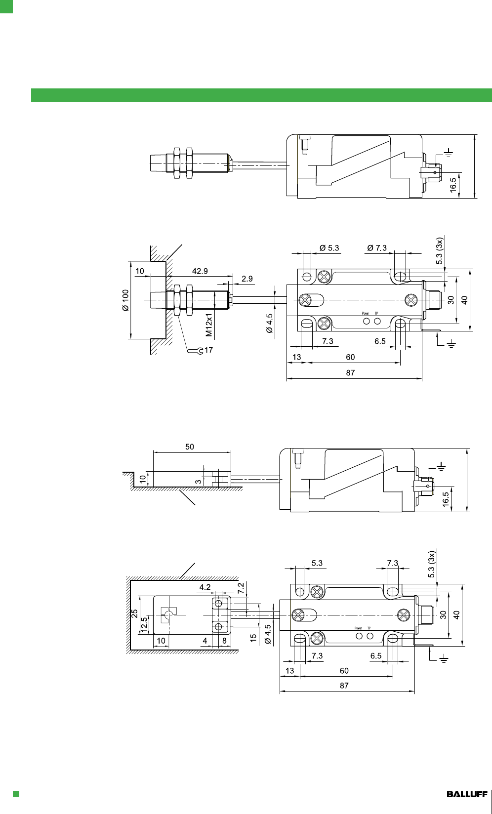
Fig. 1: BIS L-409-045-001-07-S4 with integrated read head, dimensions in mm
A Clear zone
Attach the processor using 4 M4 screws.
Note maximum tightening torque of 15 Ncm.
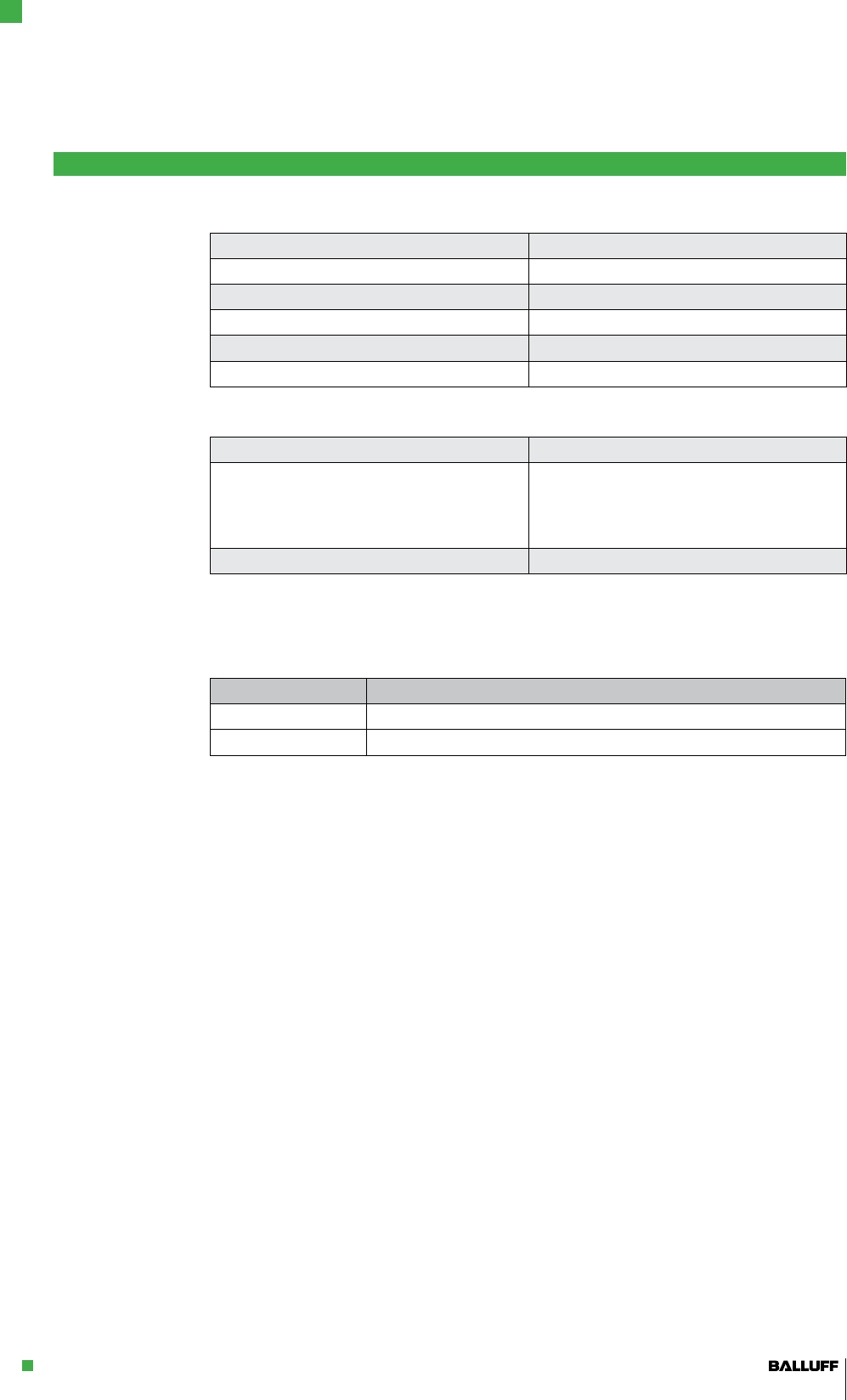
In addition to the processor with integrated read head, the following processors with remote read
head are available.
The processors with remote read head are also tightened using 4 M4 screws to a max. tighten-
ing torque of 15 Ncm:
A
41
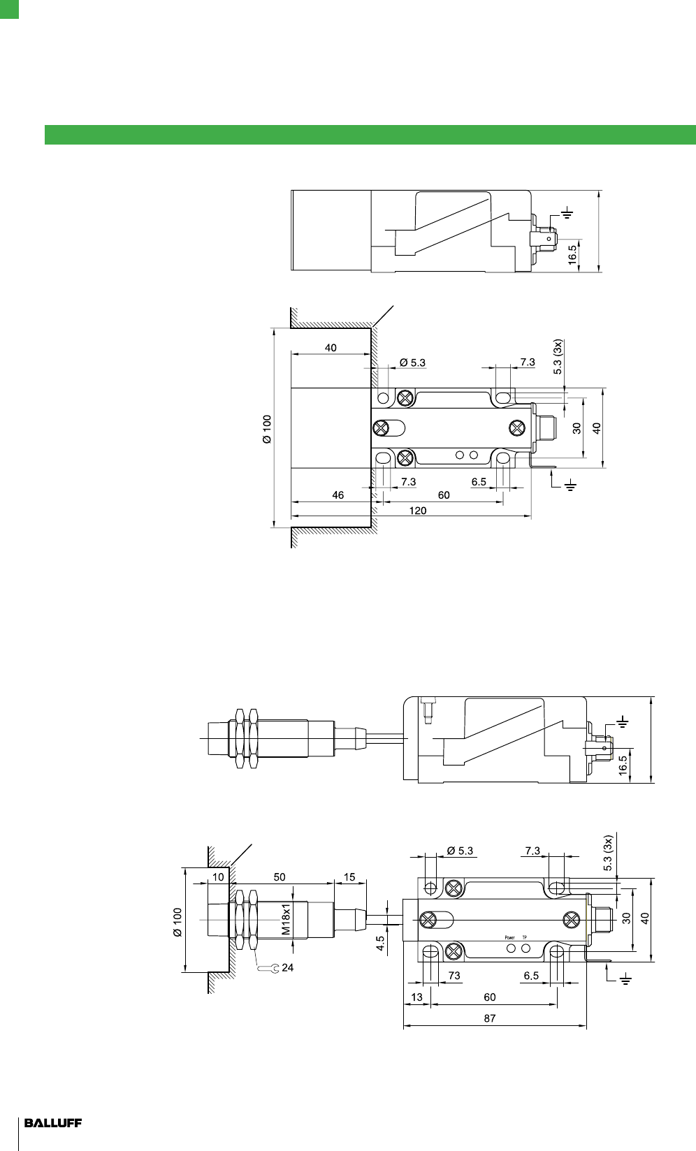
Fig. 2: Processor BIS L-409-045-002-07-S4, dimensions in mm
A Clear zone
►
BIS L-409 IO-Link Device
Processor
www.balluff.com 9
A
41
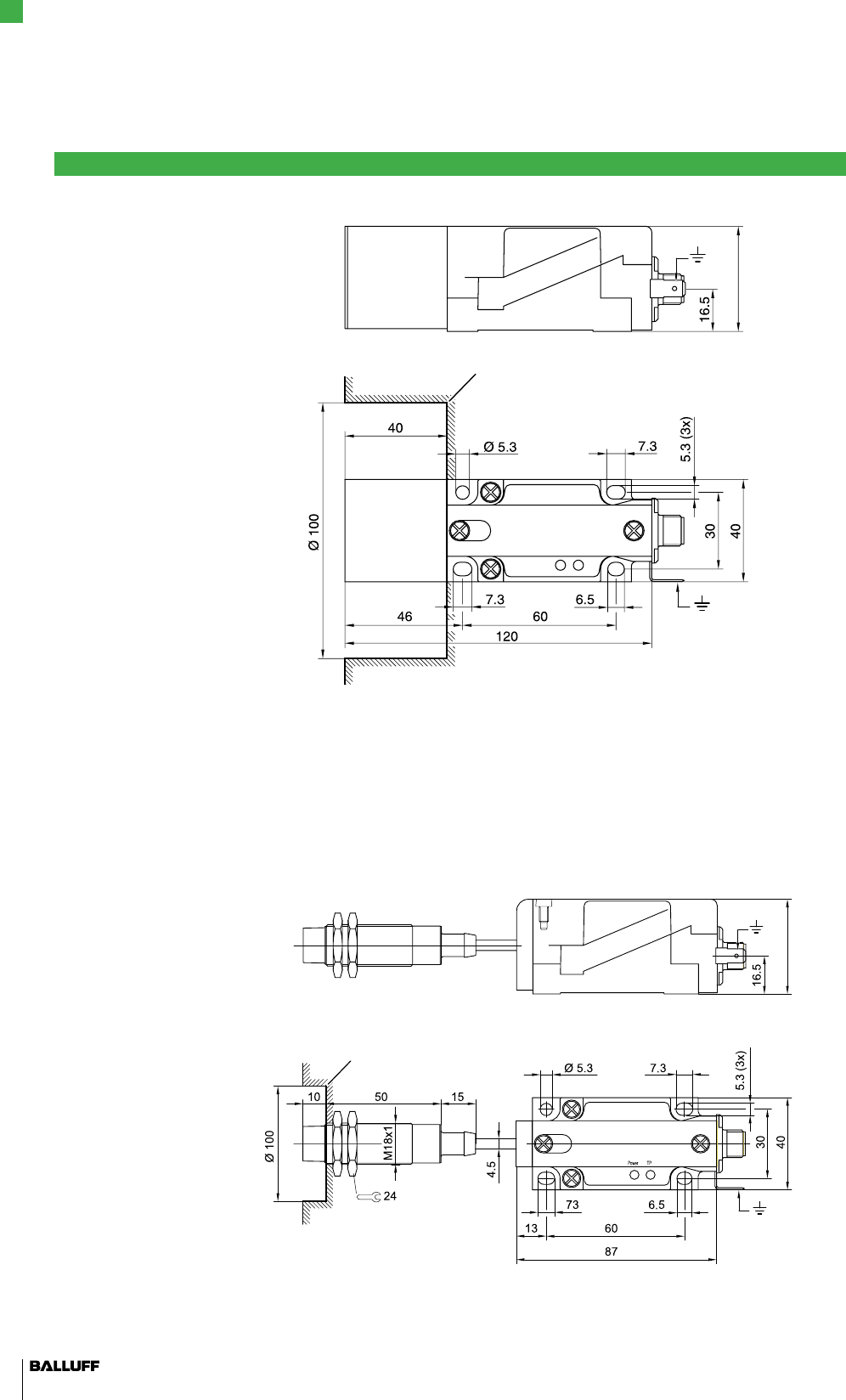
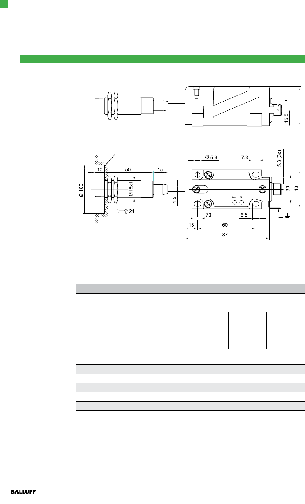
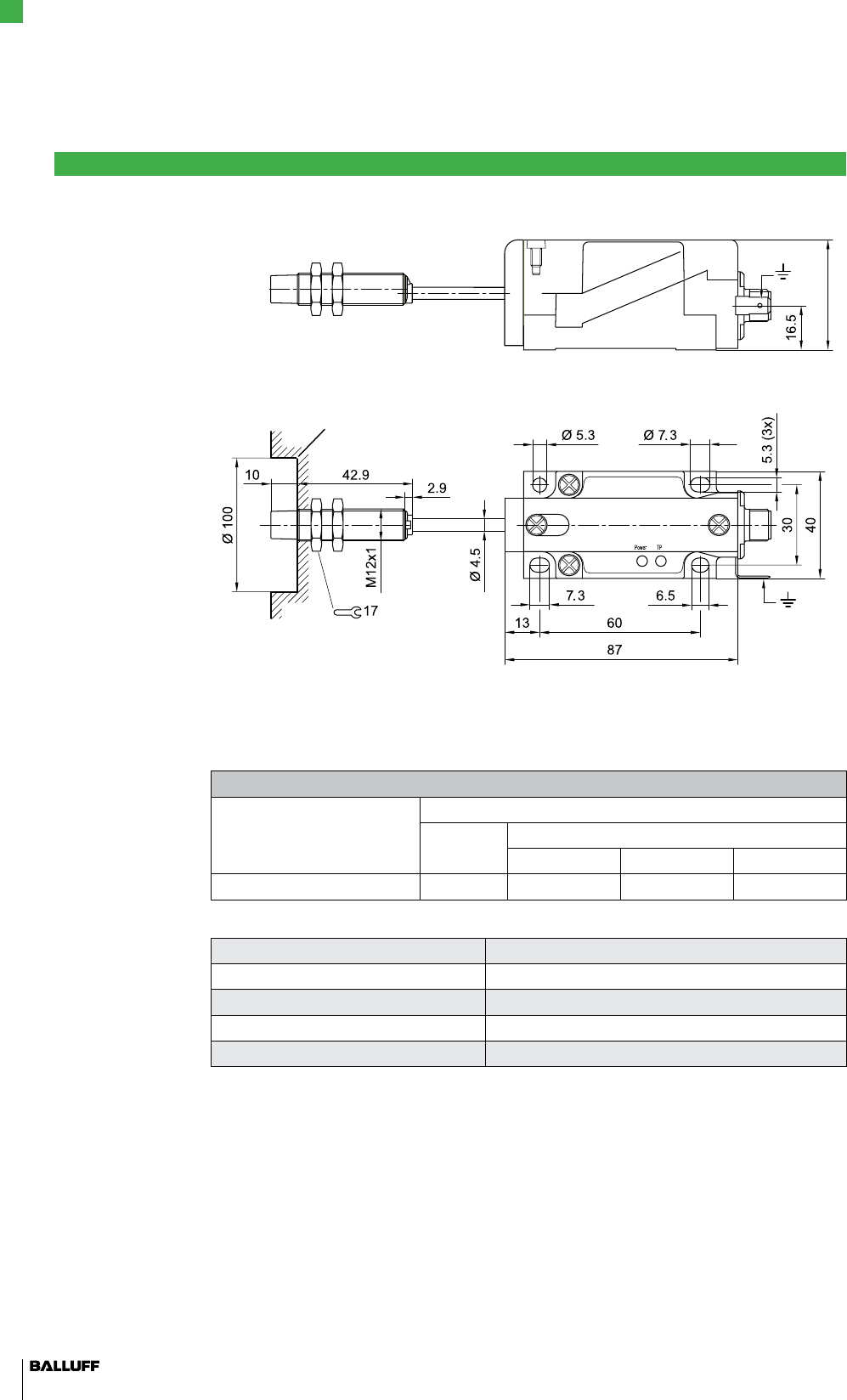
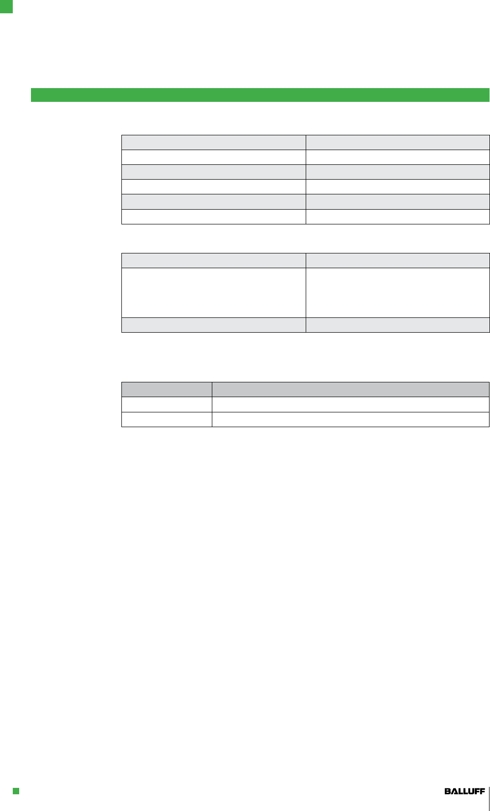
Fig. 3: Processor BIS L-409-045-003-07-S4, dimensions in mm
A Clear zone
A
A
41
Fig. 4: Processor BIS L-409-045-004-07-S4, dimensions in mm
A Clear zone
Getting Started
3
BIS L-409 IO-Link Device
Processor
10
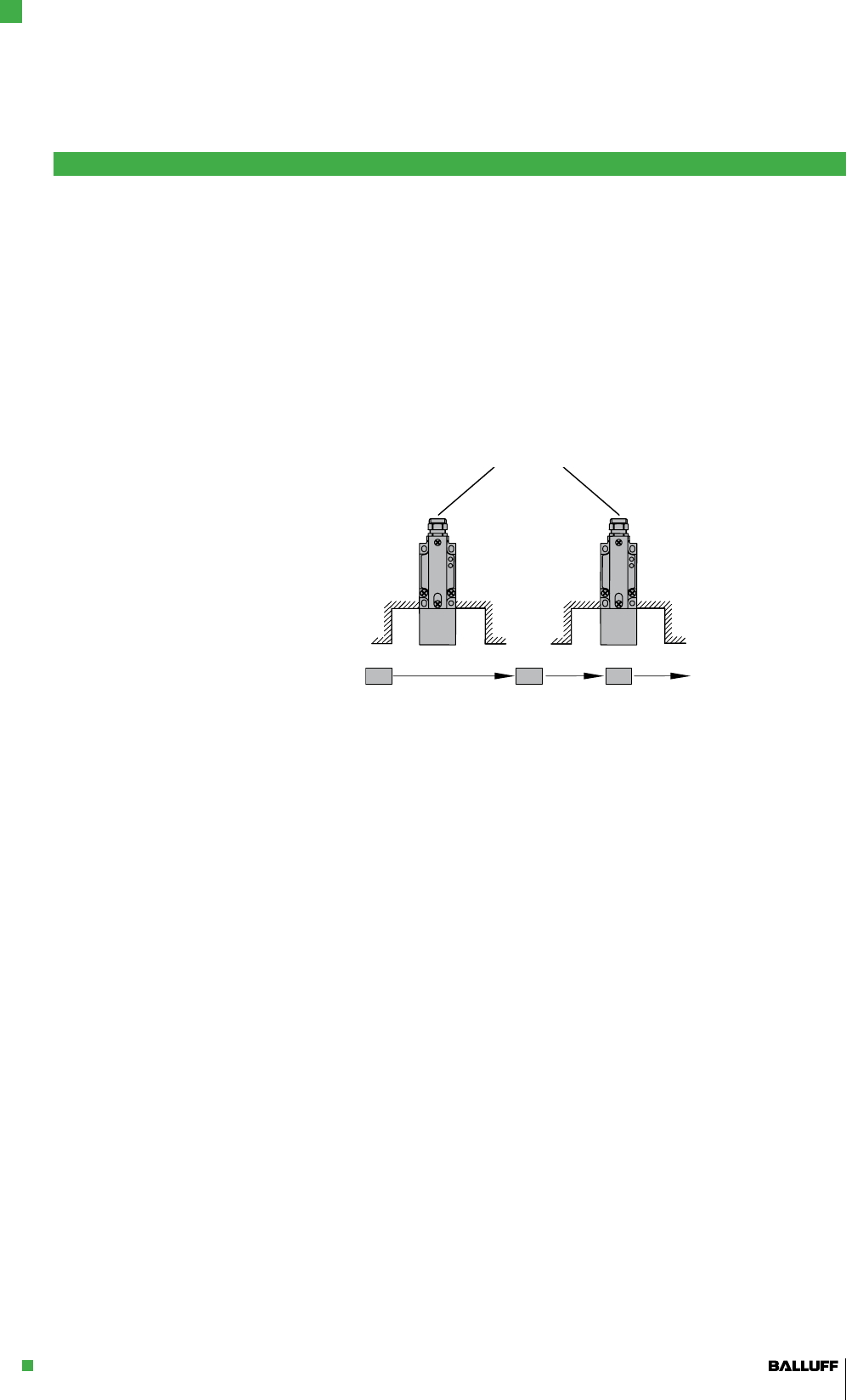
Data carrier Distance
BIS L-200-03/L > 25 cm
BIS L-100-05/L
BIS L-201-03/L > 30 cm
BIS L-101-05/L
BIS L-202-03/L > 40 cm
BIS L-102-05/L
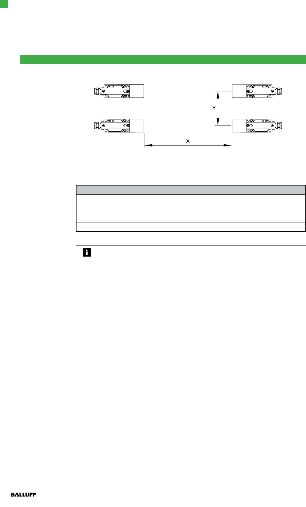
Fig. 5: Distance between two processors, see table for legend
The following distances between individual BIS L-409_... systems must be maintained:
Processor Distance x Distance Y
BIS L-409-...-001- ... 1 m 1 m
BIS L-409-...-002- ... 0.5 m 0.3 m
BIS L-409-...-003- ... 0.5 m 0.3 m
BIS L-409-...-004- ... 0.5 m 0.3 m
Note
When installing two BIS L-409-... on metal there is normally no mutual interference.
Unfavorable use of a metal frame can result in problems when reading a data carrier.
In this case the read distance is reduced to 80% of the maximum value.
In critical applications a pre-test is recommended.
Distance
between data
carriers
Distance
between
processors
Getting Started
3
BIS L-409 IO-Link Device
Processor
www.balluff.com 11
7
8
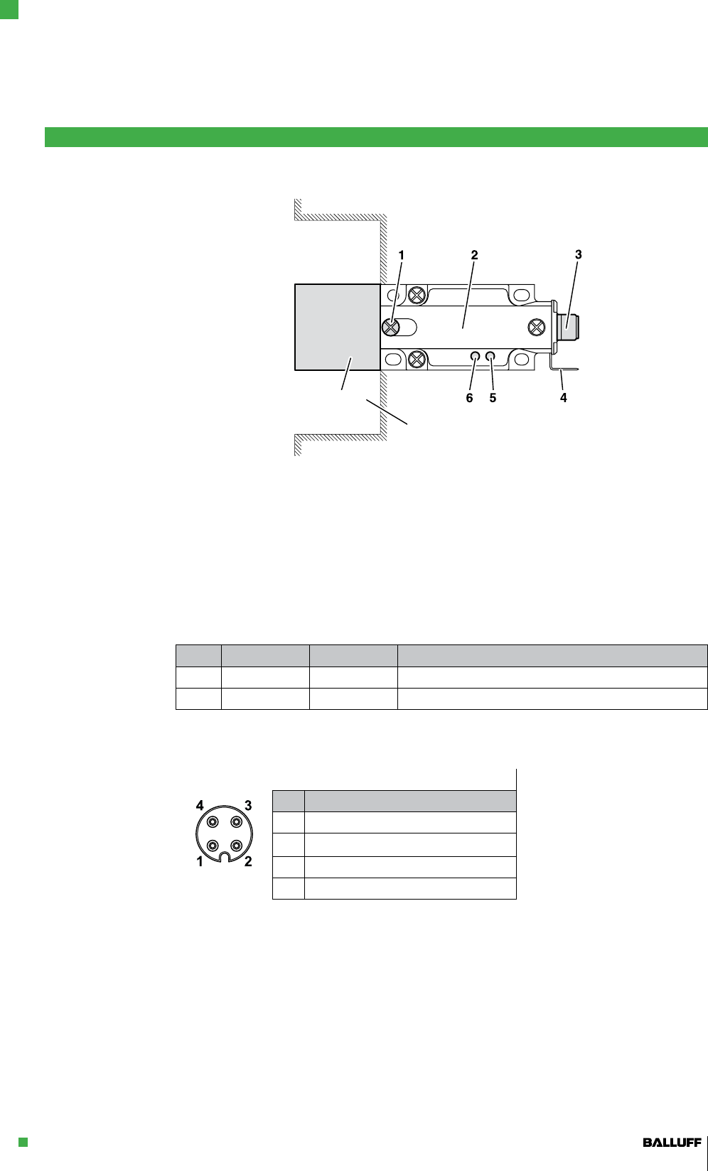
Fig. 6: Overview of processor BIS L-409-045-001-07-S4
1 Locking screw
2 BIS L-409-045-001-07-S4
3 IO-Link connection
4 Ground connection
5 LED 1
6 LED 2
7 Clear zone
8 Read head
LED indicators on the processor:
Item LED Display Function
3 LED 1 green Supply voltage present
4 LED 2 yellow Tag Present
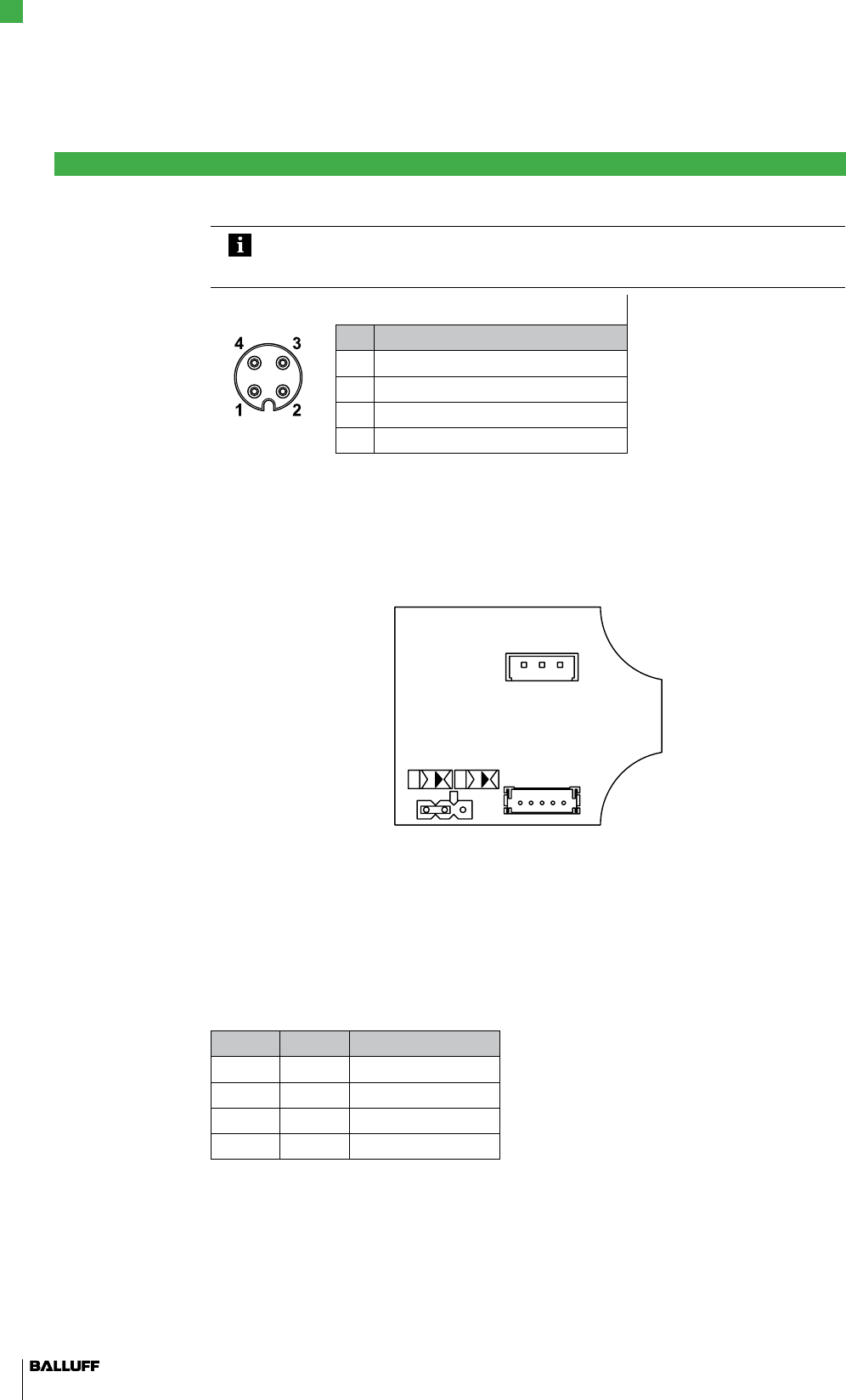
IO-Link port (M12, A-coded, female)
PIN Function
1 +24 V
2 NC
3 GND
4 C/Q
Connect data line to IO-Link Master.
(See Balluff IO-Link catalog for connection cable and accessories)
►
3.2 Electrical
connection
LED indicators
Data line
Getting Started
3
BIS L-409 IO-Link Device
Processor
12
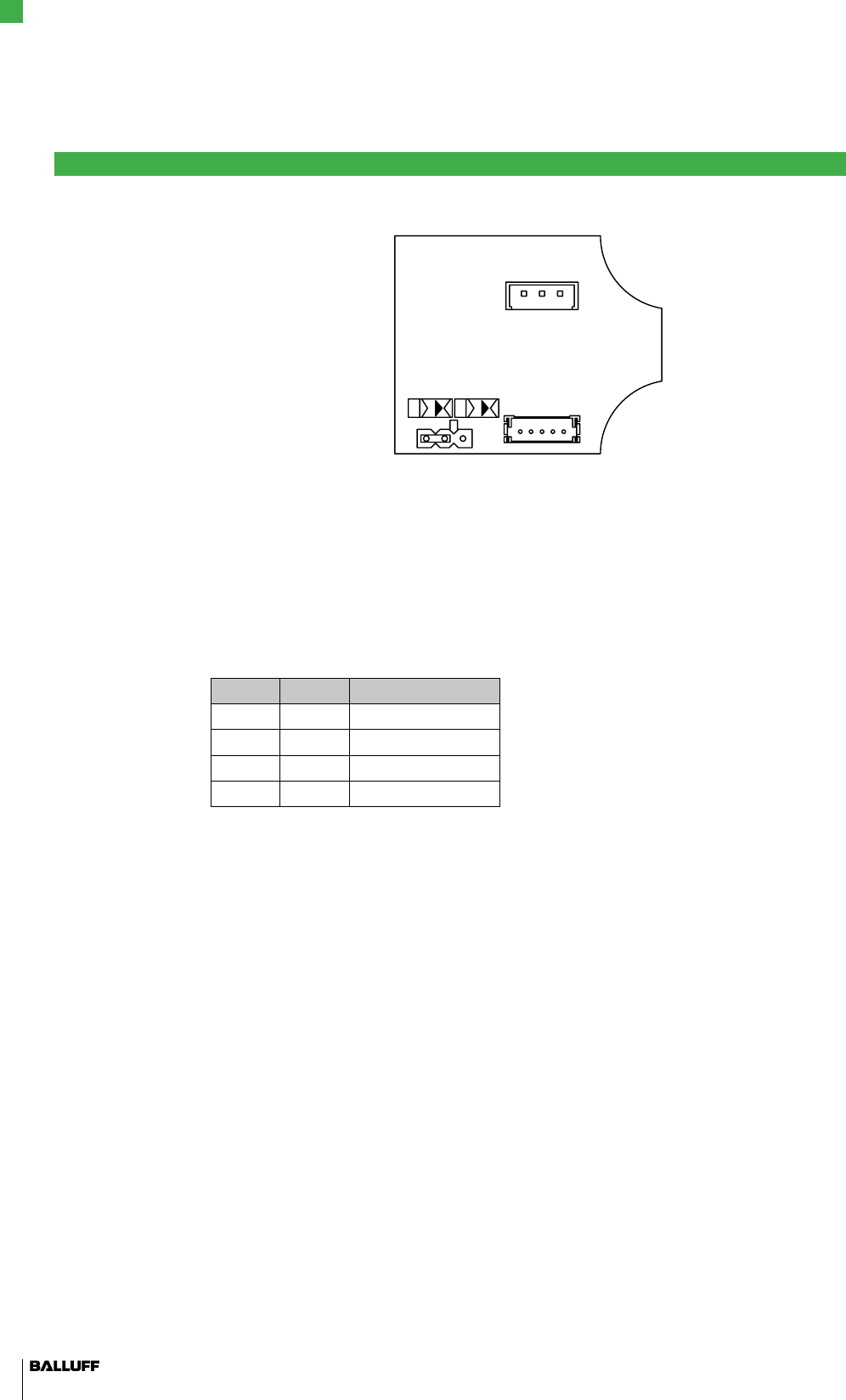
ON
S101
ON
X1
S102
X3
X4
Fig. 7: Overview of BIS L-409-... processor
1 X1 - Device terminal
2 X3 - Read head terminal
3 X4 - Jumper for operating mode
4 S101/S102 - baud rate setting
The operating mode is set using jumpers in the processor (X4):
IO-Link mode, jumper setting as shown in Fig. 7 (factory default setting)
Service mode - to be used only by Balluff service
The baud rate is set using two DIP switches S101 and S102:
S102 S101 Baud rate
OFF OFF com1 4k8
OFF ON com1 4k8
ON OFF com2 38k4 *)
ON ON com3 230k4
*) Factory default setting
–
–
Operating mode/
baud rate
Getting Started
3
BIS L-409 IO-Link Device
Processor
www.balluff.com 13
4.1 Function
principle of
Identification
Systems
The BIS L-409-... Identification System is a non-contact read-only system. The compact proces-
sor consists of processing circuitry with a fixed read head.
The system may be used to read information which has been permanently programmed into the
data carrier and to send current status messages to the controller.
The main components of the BIS L-409-... Identification System are:
Processor,
read head,
data carriers.
Data transmission to the controlling system is accomplished using an IO-Link Master.
A
Fig. 8: Schematic representation of an identification system
The data carrier is an autonomous unit which is supplied with power by the read head. The read
head continuously sends a carrier signal which is picked up by the data carrier from within a
certain distance. As soon as the data carrier is powered up by the carrier signal, a static read
operation takes place.
The processor manages the data transfer between read head and data carrier, serves as a buffer
storage device, and sends the data to the host controller.
The data are passed to the IO-Link Master using IO-Link protocol, and the Master then passes
them to the controlling system.
Host systems may be the following:
A control computer (e.g. industrial PC),
a PLC.
The main areas of application are:
In production for controlling material flow (e.g. in model-specific processes), in workpiece
transport with conveying systems, for acquiring safety-relevant data.
warehousing for monitoring material movement,
transportation, and
conveying technology.
–
–
–
–
–
–
–
–
–
Basic knowledge
4
BIS L-409 IO-Link Device
Processor
Data carrier BIS L-2…
Connection to
IO-Link Master
14
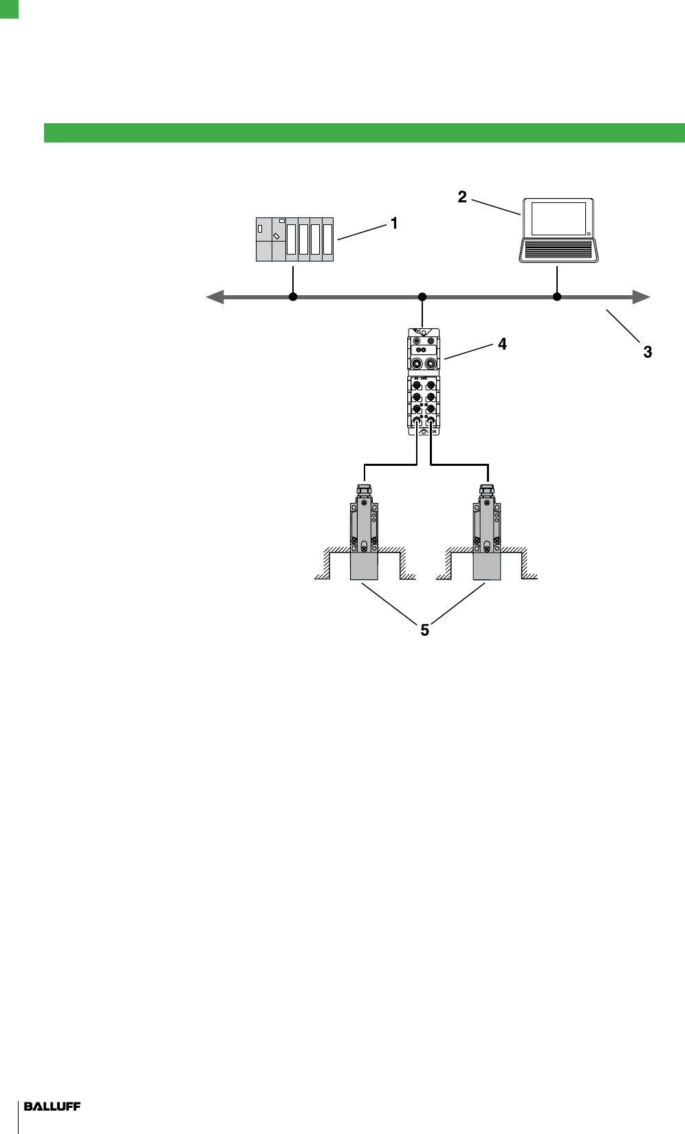
Fig. 9: BIS L-409… topology
1 PLC
2 PC
3 ProfiBus
4 IO-Link Master
5 Processors BIS L-409…
4.2 System topology
Basic knowledge
4
BIS L-409 IO-Link Device
Processor

www.balluff.com 15
Basic knowledge
4
4.3 Read distance/
offset
4.4 Product
description
4.5 Data security
4.6 IO-Link basic
knowledge
To ensure that data carriers are recognized without error and the data can be reliably read, do
not exceed a maximum distance and maximum offset between the data carriers and read heads
(see “Technical Data” starting page 16).
The “distance” specification refers to the maximum distance from the data carrier to the sensing
surface of the read head.
The “offset” specification indicates the maximum offset between the center axis of the data
carrier and the center axis of the sensing surface.
Data carriers can only be reliably recognized and the data reliably read within the permissible
read distance and offset. In the border area an unstable condition may occur, so that a data
carrier is alternately recognized and lost.
Data carrier recognition is indicated by an LED on the device (“TP – Tag Present”, see “Technical
Data” starting page 16). At the same time the CP bit is set in the input buffer (“CP – Codetag
Present”, see “Process Data” starting page 42).
Processor BIS L-409-045-…-07-S4:
Plastic housing,
circular connector terminations,
one read head connected,
the read head suitable for dynamic or static operation,
data carrier is powered by the read head using a carrier signal.
In order to ensure data integrity, data transmission between the data carrier and processor can
be monitored using a check procedure.
In the processor a CRC_16 data check can be configured.
If the CRC check is enabled, the data carrier data are checked using a 2-byte CRC_16 check-
sum. If the checksum does not agree with the checked data, an error message is sent.
Note
The CRC_16 data check can only be used with data carriers of type BIS L-10X-05/L
The data carriers must be initialized using a BIS L-60_ _ processor and the
BISCOMRW.EXE PC software or a portable reader BIS L-81_ (refer to the User's
guide for the corresponding device for this procedure).
The manufacturer-specific standard IO-Link sends not only the actual process signal, but also all
relevant parameter and diagnostics data on the process level over a single standard cable.
Communication is based on a standard UART protocol with 24V pulse modulation; no separate
power supply is required. Connection is possible using a 2-conductor or 3-conductor cable.
Advantages of IO-Link:
Uniform, simple wiring of different devices
Controlling system can be used to change the device parameters
Remote querying of diagnostics information is possible
Centralized data retention of the device parameters is possible
–
–
–
–
–
–
–
–
–
BIS L-409 IO-Link Device
Processor
16
BIS L-409-045-
001-07-S4
Dimensions
Characteristic
data
Mechanical data
Technical Data
5
A
41
Fig. 10: Dimensions for BIS L-409-045-001-07-S4 processor [mm]
A Clear zone
BIS L-409-045-001-07-S4
Characteristic data when used
with data carriers (installed in
clear zone)
When v = 0 (static)
Distance
[mm] read
Offset from center axis at distance: [mm]
0 - 20 0 - 35 0 - 45 0 - 15
BIS L-200-03 / BIS L-100-05 25 15 – – –
BIS L-201-03 / BIS L-101-05 35 – 20 – –
BIS L-202-03 / BIS L-102-05 48 – – 25 –
BIS L-203-03 / BIS L-103-05 16 – – – 10
Housing material Plastic (PBT)
Wiring Connector, M12 4-pin, A-coded
Enclosure rating IP65 (with connectors)
Weight 220 g
BIS L-409 IO-Link Device
Processor
www.balluff.com 17
Operating voltage VS 24 V DC +10/-20 %
Ripple ≤ 10 %
Current draw ≤ 150 mA
Load current capacity in SIO mode max. 50 mA
Output C/Q Short circuit protected
Device interface IO-Link
Ambient temperature range 0 °C … +70 °C
EMV
EN 301 489-1/-3
EN 61000-4-2/-3/-4/-5/-6
EN 300 330-1
–
–
–
Class A
Level 3A/3A/4A/2A/3A
Power class 5
–
–
–
Vibration/shock EN 60068 Part 2-6/27/29/64/32
Two LEDs on the communications module indicate the status:
LED indicator Function
LED green Supply voltage present
LED yellow Data carrier within read range (Tag Present)
Electrical data
Operating
conditions
Function
indicators
Technical data
5
BIS L-409 IO-Link Device
Processor
18
A
41
Fig. 11: Dimensions for BIS L-409-045-002-07-S4 processor [mm]
A Clear zone
BIS L-409-045-002-07-S4
Characteristic data when used
with data carriers (installed in
clear zone)
When v = 0 (static)
Distance
[mm] read
Offset from center axis at distance: [mm]
0 - 10 0 - 15 0 - 20
BIS L-200-03 / BIS L-100-05 15 10 – –
BIS L-201-03 / BIS L-101-05 18 12 12 –
BIS L-203-03 / BIS L-103-05 10 4 – –
Housing material Plastic (PBT)
Read head housing material CuZn nickel plated
Wiring Connector, M12 4-pin, A-coded
Enclosure rating IP67
Weight 200 g
BIS L-409-045-
002-07-S4
Dimensions
Characteristic
data
Mechanical data
Technical data
5
BIS L-409 IO-Link Device
Processor

www.balluff.com 19
Operating voltage VS 24 V DC +10/-20 %
Ripple ≤ 10 %
Current draw ≤ 150 mA
Load current capacity in SIO mode max. 50 mA
Output C/Q Short circuit protected
Device interface IO-Link
Ambient temperature range 0 °C … +70 °C
EMV
EN 301 489-1/-3
EN 61000-4-2/-3/-4/-5/-6
EN 300 330-1
–
–
–
Class A
Level 3A/3A/4A/2A/3A
Power class 5
–
–
–
Vibration/shock EN 60068 Part 2-6/27/29/32/64
Two LEDs on the communications module indicate the status:
LED indicator Function
LED green Supply voltage present
LED yellow Data carrier within read range (Tag Present)
Electrical Data
Operating
conditions
Function
indicators
Technical data
5
BIS L-409 IO-Link Device
Processor
20
A
41
Fig. 12: Dimensions for BIS L-409-045-003-07-S4 processor [mm]
A Clear zone
BIS L-409-045-003-07-S4
Characteristic data when
used with data carriers
(installed in clear zone)
When v = 0 (static)
Distance
[mm] read
Offset from center axis at distance: [mm]
0 - 5 0 - 8 0 - 11
BIS L-203-03 / BIS L-103-05 7 4 – –
Housing material Plastic (PBT)
Read head housing material*) CuZn nickel plated
Wiring Connector, M12 4-pin, A-coded
Enclosure rating IP67
Weight 170 g
BIS L-409-045-
003-07-S4
Dimensions
Characteristic
data
Mechanical data
Technical data
5
BIS L-409 IO-Link Device
Processor

www.balluff.com 21
Operating voltage VS 24 V DC +10/-20 %
Ripple ≤ 10 %
Current draw ≤ 150 mA
Load current capacity in SIO mode max. 50 mA
Output C/Q Short circuit protected
Device interface IO-Link
Ambient temperature range 0 °C … +70 °C
EMV
EN 301 489-1/-3
EN 61000-4-2/-3/-4/-5/-6
EN 300 330-1
–
–
–
Class A
Level 3A/3A/4A/2A/3A
Power class 5
–
–
–
Vibration/shock EN 60068 Part 2-6/27/29/32/64
Two LEDs on the communications module indicate the status:
LED indicator Function
LED green Supply voltage present
LED yellow Data carrier within read range (Tag Present)
Electrical Data
Operating
conditions
Function
indicators
Technical data
5
BIS L-409 IO-Link Device
Processor
22
BIS L-409-045-
004-07-S4
Dimensions
Characteristic
data
Mechanical data
A
A
41
Fig. 13: Dimensions for BIS L-409-045-004-07-S4 processor [mm]
A Clear zone
BIS L-409-045-004-07-S4
Characteristic data when used
with data carriers (installed in
clear zone)
When v = 0 (static)
Distance
[mm] read
Offset from center axis at distance: [mm]
0 - 10 0 - 15 0 - 20
BIS L-200-03 / BIS L-100-05 15 10 – –
BIS L-201-03 / BIS L-101-05 18 12 12 –
BIS L-203-03 / BIS L-103-05 10 4 – –
Housing material Plastic (PBT)
Read head housing material CuZn nickel plated
Wiring Connector, M12 4-pin, A-coded
Enclosure rating IP67
Weight 170 g
Technical data
5
BIS L-409 IO-Link Device
Processor
www.balluff.com 23
Electrical Data
Operating
conditions
Function
indicators
Operating voltage VS 24 V DC +10/-20 %
Ripple ≤ 10 %
Current draw ≤ 150 mA
Load current capacity in SIO mode max. 50 mA
Output C/Q Short circuit protected
Device interface IO-Link
Ambient temperature range 0 °C … +70 °C
EMV
EN 301 489-1/-3
EN 61000-4-2/-3/-4/-5/-6
EN 300 330-1
–
–
–
Class A
Level 3A/3A/4A/2A/3A
Power class 5
–
–
–
Vibration/shock EN 60068 Part 2-6/27/29/32/64
Two LEDs on the communications module indicate the status:
LED indicator Function
LED green Supply voltage present
LED yellow Data carrier within read range (Tag Present)
Technical data
5
BIS L-409 IO-Link Device
Processor
24
6.1 Installation
A
41
Fig. 14: Processor with integrated read head BIS L-409-045-001-07-S4 (dimensions in mm)
A Clear zone
Attach processor using four M4 screws
Note maximum tightening torque of 15 Ncm.
Processors with remote read head are also tightened using 4 M4 screws to a max. tightening
torque of 15 Ncm:
A
41
Fig. 15: Processor BIS L-409-045-002-07-S4 (dimensions in mm)
A Clear zone
►
Installation
6
BIS L-409 IO-Link Device
Processor
www.balluff.com 25
A
41
Fig. 16: Processor BIS L-409-045-003-07-S4 (dimensions in mm)
A Clear zone
A
A
41
Fig. 17: Processor BIS L-409-045-004-07-S4 (dimensions in mm)
A Clear zone
Installation
6
BIS L-409 IO-Link Device
Processor
26
Fig. 18: Distance between processors
The following distances between individual BIS L-409_... systems must be maintained:
Processor Distance x Distance Y
BIS L-409-...-001- ... 1 m 1 m
BIS L-409-...-002- ... 0.5 m 0.3 m
BIS L-409-...-003- ... 0.5 m 0.3 m
BIS L-409-...-004- ... 0.5 m 0.3 m
Note
When installing two BIS L-409-... on metal there is normally no mutual interference.
Unfavorable use of a metal frame can result in problems when reading a data carrier.
In this case the read distance is reduced to 80% of the maximum value.
In critical applications a pre-test is recommended!
Distance
between
processors
Installation
6
BIS L-409 IO-Link Device
Processor
www.balluff.com 27
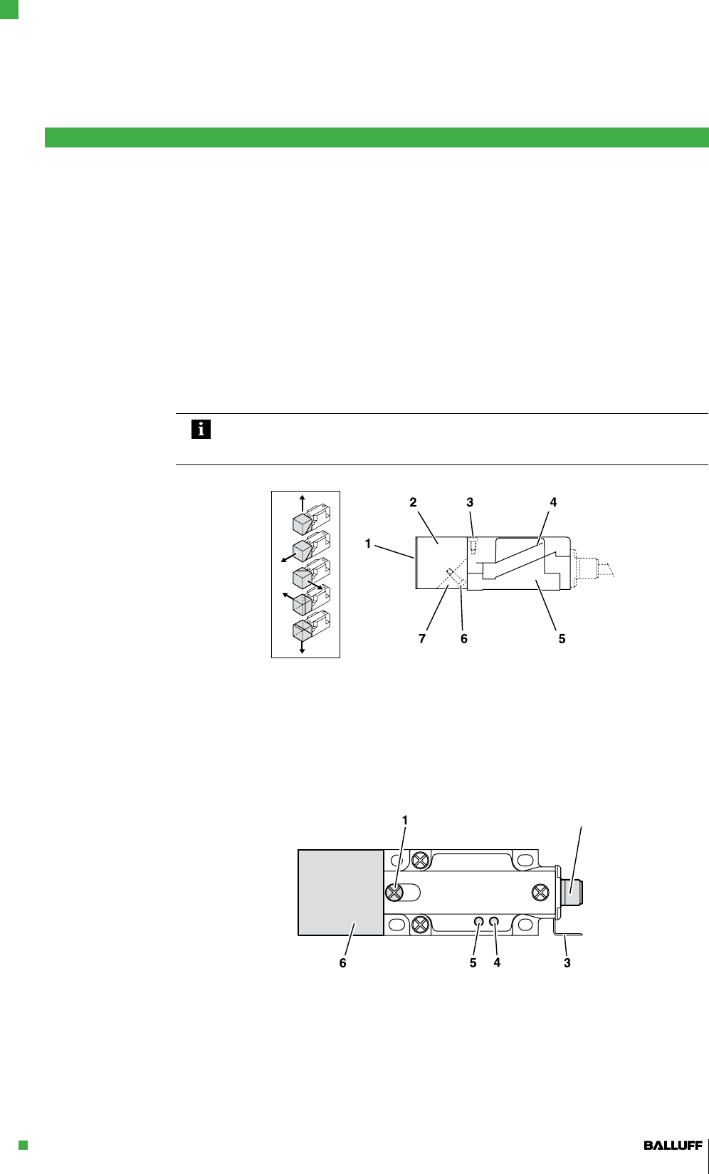
The read head of the processor consists of a read head module and read head carrier.
The sensing face of the read head can be positioned as desired (see Fig. 19).
Rotating the sensing face from front to up or to the side:
Unscrew both screws (6) on the read head carrier (7).
Rotate read head module (2) by 180°.
Tighten both screws (6).
Rotating the read head:
Loosen locking screw (3).
Turn read head to the desired position.
The read head can be rotated steplessly by 270°.
Tighten locking screw (3).
Note
The read head module is protected against overtightening.
The read head modules are not interchangeable.
Fig. 19: Sensing face positions
1 Sensing face
2 Read head module
3 Locking screw
4 Module BIS L-400
5 Mounting base
6 Screw
7 Read head carrier
2
Fig. 20: Processor BIS L-409-... overview
1 Locking screw
2 IO-Link connection
3 Ground
4 LED 1
5 LED 2
6 Read head
►
►
►
►
►
⇒
►
Orienting the
read head
6.2 Electrical
connection
Installation
6
BIS L-409 IO-Link Device
Processor
28
Note
Make the ground connection, depending on the system, either directly or using an RC
combination to ground.
IO-Link port (M12, A-coded, female)
PIN Function
1 +24 V
2 NC
3 GND
4 C/Q
Connect data line to IO-Link Master.
(See Balluff IO-Link catalog for connection cable and accessories)
The operating mode and the baud rate are set in the processor using jumpers and DIP switches.
ON
S101
ON
X1
S102
X3
X4
Fig. 21: Processor BIS L-409-... overview
1 X1 - Device terminal
2 X 3 - Read head terminal
3 X4 - Jumper for operating mode
4 S101/S102 - baud rate setting
The operating mode is set using jumpers in the processor (X4):
IO-Link mode, jumper setting as shown in Fig. 21 (factory default setting)
Service mode - to be used only by Balluff service
The baud rate is set using two DIP switches S101 and S102:
S102 S101 Baud rate
OFF OFF com1 4k8
OFF ON com1 4k8
ON OFF com2 38k4 *)
ON ON com3 230k4
*) Factory default setting
►
–
–
IO-Link
connection
6.3 Hardware
settings
Installation
6
BIS L-409 IO-Link Device
Processor
www.balluff.com 29
7.1 Digital point-to-
point connection
Three-conductor
physics
Communications
mode
Interleave mode
IO-Link integrates conventional and intelligent actuators and sensors into automation systems.
Mixed use of traditional and intelligent devices is possible with no additional effort.
IO-Link is intended as a communications standard below the traditional fieldbus level. Fieldbus-
neutral IO-Link transmission uses existing communications systems (fieldbuses or Ethernet-
based systems).
The actuators and sensors are connected in point-to-point using conventional unshielded
cables.
IO-Link devices can send application-specific parameters and data (e.g. diagnostics data) using
a serial communications procedure. Flexible telegrams are possible for sending larger quantities
of data. Communication is based on a standard UART protocol with 24V pulse modulation. Only
one data line is used, which carries both the controller as well as the device telegram. This
means that conventional 3-conductor physics is possible.
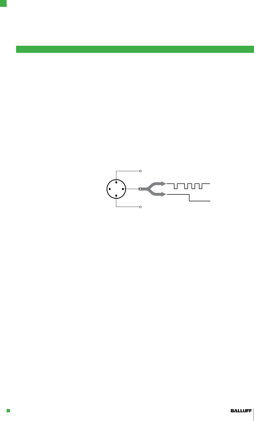
IO-Link supports both communication mode as well as standard IO mode (SIO). Standard IO
provides a switching signal on the communication line such as used by normal binary switching
sensors. This mode is only possible with devices using 3-conductor connection technology.
Fig. 22: 3-conductor physics of IO-Link
The BIS L-409-... supports both modes. In SIO mode the signal “Data carrier in range” (24V) and
“No data carrier in range” (0 V) is made available to the host system as a switching signal.
If the BIS L-409… is not used with an IO-Link Master and without triggering IO-Link communica-
tion, it works in SIO mode and can be operated on a digital input.
The BIS L-409-... works in communication mode with Frame Type 1. In this transmission type 2
bytes of process data or required data are sent per frame (data block). This can take place either
from IO-Link Master to device or vice-versa. Process data are the application-specific data, and
required data may contain parameters, service or diagnostic data.
So-called “Interleave Mode” makes it possible to send larger quantities of data. There multiple
Type 1 frames must be combined into a sequencer. One frame with process data and one with
required data are sent in alternation.
With the BIS L-409 a sequence consists of 32 individual frames. 8 bytes of process data are
sent in each direction per sequence. These process data are shown in greater detail in Section
10.4 “Protocol sequence” on page 42.
IO-Link Basics
7
BIS L-409 IO-Link Device
Processor
30
7.2 Process data
container
7.3 Direct parameter
page
The IO-Link protocol provides a process data container 32 bytes in size. Addressing is done in
the command byte which the IO-Link Master sends. When process data are sent, addressing is
directly to the sub-indices 00hex … 1Fhex.
The BIS L-409-… processes 8 bytes of input and 8 bytes of output data (input buffer/output
buffer). The process data are mapped to the first 8 bytes of the process data container (sub-
indices 00hex…07hex).
IO-Link protocol
Subaddress
BIS L-409 IO-Link Device
Subaddress
00hex ⇒00hex
...
...
...
07hex ⇒07hex
08hex
...
1Fhex
The Direct Parameter Page (DPP) contains 32 bytes of application-specific parameters and
parameters for setting IO-Link communication. This corresponds to the first two pages of the
Service Protocol Data Unit (SPDU) with 16 bytes each. Although the SPDU of the BIS L-409
devices is not supported, access to the DPP is made via Index, Subindex and length (in bytes) of
the SPDU.
With Subindex 0 all 16 bytes of the Index can be accessed; the length determines how many
parameters are read or written. With a Subindex > 0 a particular element of the Index is
accessed, and the length specification is not used. Specification of these values depends on the
IO-Link Master and the controller.
The most important parameters are summarized in the following table. Each parameter has a
data width of 1 byte.
DPP SPDU Parameter Access BIS
L-409
Meaning
Address Index Sub-
index
00hex 0 1 Master
Command
R/W - Determines the mode:
5Ahex: Standard-IO mode
97hex: Restart communication
98hex: Communication running,
output data valid1)
99hex: Communication running,
output data invalid2)
01hex 0 2 Master
Cycle Time
R/W - Used cycle time, specified by IO-
Link master
02hex 0 3 Min. Cycle
Time
R3) Minimum cycle time achievable by
the device
03hex 0 4 Frame
Capability
R 02hex The device supports Frame Type 1
Legend:
W: Write
R: Read
1) Device accepts output data from the
master.
2) Device does not accept output data
from the master and uses the last valid
output data.
3) 25hex at 230.4 kbaud
35hex at 38.4 kbaud
62hex at 4.8 kbaud
IO-Link Basics
7
BIS L-409 IO-Link Device
Processor
www.balluff.com 31
Direct parameter
page (cont.)
DPP SPDU Parameter Access BIS
L-409
Meaning
Address Index Sub-
index
04hex 0 5 IO Link
Revision
R 10hex Version of the IO-Link spec match-
ing the device: 10hex = V1.0
05hex 0 6 Process
Data In
R 07hex 8 bytes of process data (Device to
Master, SIO mode is supported)
06hex 0 7 Process
Data Out
R 87hex 8 bytes of process data (Master to
device, SIO mode is not supported)
07hex 0 8 Vendor ID 1 R 03hex Vendor-ID:
0378hex = Balluff GmbH
08hex 0 9 Vendor ID 2 R 78hex
09hex 0 10 Device ID 1 R 06hex Device-ID:
060101hex =
BIS L-409-045-…-07-S4
0Ahex 0 11 Device ID 2 R 01hex
0Bhex 0 12 Device ID 3 R 01hex
10hex
...
1Bhex
11) Device
Specific
Parameters
R/W - 1)
Legend: W: Write
R: Read
1) See “Parameterizing the processor”
starting page 32
Note
The output buffer process data are only valid if the device is using “Master Command”
98hex.
IO-Link Basics
7
BIS L-409 IO-Link Device
Processor
32
8.1 Required data
Saving the
parameters
Setting the processor parameters
8
BIS L-409 IO-Link Device
Processor
The device-specific parameters for the identification system application are in addresses 10hex ...
12hex. The parameter data are described in greater detail in the following.
DPP SPDU Parameter Data
width
Value
range
Default value
Address Index Subindex
Identification data
07hex 0 8 Vendor ID 2 bytes
Read only
0378hex
08hex 0 9
09hex 0 10
Device ID 3 Byte 060101hex0Ahex 0 11
0Bhex 0 12
Parameter data
10hex 1 1 CRC_16 check 1 byte 0/1 0
11hex 1 2 BIS L-10x-05 1 byte 0/1 0
12hex 1 3 Data comparison
counter 1 byte 1...10 2
The parameters can be accessed on the parameter data channel using Index, Subindex and
length (in bytes). With Subindex 0 all 16 bytes of the Index can be accessed; the length deter-
mines how many parameters are read or written. With a Subindex > 0 a particular element of the
Index is accessed, and the length specification is not used. Specification of these values
depends on the IO-Link Master and the controller.
There are parameters which can only be read, while others can be read and written (see “Direct
Parameter Page” on page 30).
Note
The values of the unused device-specific parameters 13hex to 1Bhex must be set to
“0”.
The configured parameters are immediately valid as soon as they are set. However, if there is a
power loss the user-defined settings will be lost. The device is restarted with the factory settings,
and any other parameter setting needs to be made again.
www.balluff.com 33
8.2 Parameterization
data mapping
CRC check
Data carrier
Setting the processor parameters
8
BIS L-409 IO-Link Device
Processor
Address 10hex, CRC_16 check
The CRC check is a procedure for determining a check value in order to be able to recognize
data transmission errors. If the CRC check is activated, an error message is sent when a CRC
error is detected.
(If the parameter CRC_16 data check is set, then in addition to the data carrier data, a 2-byte
CRC_16 checksum is checked (see “Data integrity” on page 15). The data compare counter is
automatically set to one-time reading. Detection of a data carrier arriving in the read zone then
takes a maximum of 70 ms.
Note
The CRC_16 data check can only be used with data carriers of type BIS L-10X-05/L.
The data carriers must be initialized using a BIS L-60_ _ processor and the
BISCOMRW.EXE PC software or a portable reader BIS L-81_ (refer to the User's
guide for the corresponding device for this procedure).
Checksum
The checksum is written to the data carrier as 2 bytes of information. This means 2 bytes of user
data per block are sacrificed.
1 byte, Address 10hex
MSB 6 5 4 3 2 1 LSB
(not relevant) 1/0
Bit 0 (LSB) = 0: no CRC check (default setting)
Bit 0 (LSB) = 1: CRC Check
Address 11hex, BIS L-10x-05
Note
If type BIS L-10X-05 data carriers are used, parameter “BIS L-10x-05” must be
activated.
1 byte, Address 11hex
MSB 6 5 4 3 2 1 LSB
(not relevant) 1/0
Bit 0 (LSB) = 0: No type BIS L-10x-05 data carrier is used (default setting)
Bit 0 (LSB) = 1: A type BIS L-10x-05 data carrier is used

34
Data comparison
counter
Setting the processor parameters
8
BIS L-409 IO-Link Device
Processor
Address 12hex, data comparison counter
Using this parameter you can increase data integrity if the CRC_16 checksum is not used. The
processor reads the data carrier data multiple times within a read operation. The processor
stores and compares the data. Once the data carrier is recognized, the processor releases the
data. From 1 to 10 read repetitions can be set in the “Data comparison counter” field.
1 byte, Address 12hex
MSB 6 5 4 3 2 1 LSB
(not relevant) Value range: 01hex…0Ahex
Bit 0 … 3: Permissible value range 01hex … 0Ahex (decimal 1 … 10)
Default setting: 02hex (decimal: 2)
The decimal value is copied directly to the program. If an input value lies outside the permitted
value range, the default setting of 2 comparisons is used.

www.balluff.com 35
9.1 Project
administration
GSD file
Head module
Data modules
9.2 Integration into
project
administration
software
9.3 Integration
example
Installing the
GSD file
In project administration of fieldbus devices, a physical device is mapped as a modular system
consisting of a head module and multiple data modules. The device data required for project
planning are stored in GSD files (Generic Station Description).
The GSD files are made available by the vendors of the IO-Link Masters. The GSD files for Balluff
IO-Link Masters are available on the Internet at “www.balluff.com/software”
for downloading.
The data modules for an IO-Link device are shown in the project administration software by port.
The GSD file provides the possible data modules (inputs or outputs of various data width). For
configuring the IO-Link device the appropriate data modules are assigned to a particular port.
First the head module is inserted into the configuration. The head module is coded according to
the special identification format. head modules in this coding are used for identification and
parameter setting and have a data width of 2 bytes input of 2 bytes input/output data.
The data modules are arranged onto the head module in order of the slots for ports/PINs.
To integrate a BIS L-409 IO-Link device the following steps a generally required:
Load the GSD file for the IO-Link Master into the hardware configuration of the host system.
Insert the data module “Input 8 bytes/Output 8 bytes” (IOL_I/O_8/8_Byte) for the used
IO-Link port (Port X, Pin 4).
This assigns the start addresses of the input and output data. The input and output data
can, as described in Section 10, be used for operating the BIS L-409-....
Integration of a BIS L-409-IO-Link-Device is shown using the example of a BNI-PBS-IO-Link-
Master. In the example a Siemens S7 with “SIMATIC-MANAGER” program and project adminis-
tration software is used. The exact procedure will vary from case to case depending on the
software used and may differ from this example.
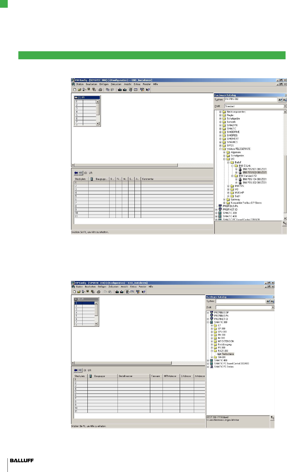
To do the project planning on the PC, the GSD file for the module must be installed:
Open new or existing project.
Open hardware configurator.
Select menu command “Tools| Install new GSD...”.
The “Install new GSD” window opens.
Select directory and GSD file.
The [Install] button only becomes active if a GSD file is selected.
Click on [Install].
The GSD file is installed.
Once the operation is finished, a message appears.
Confirm the message and close the window.
Select menu command “Tools | Update catalog”.
The modules are displayed in the project tree.
1.
2.
⇒
►
►
►
⇒
►
⇒
►
⇒
⇒
►
►
⇒
Startup
9
BIS L-409 IO-Link Device
Processor
36
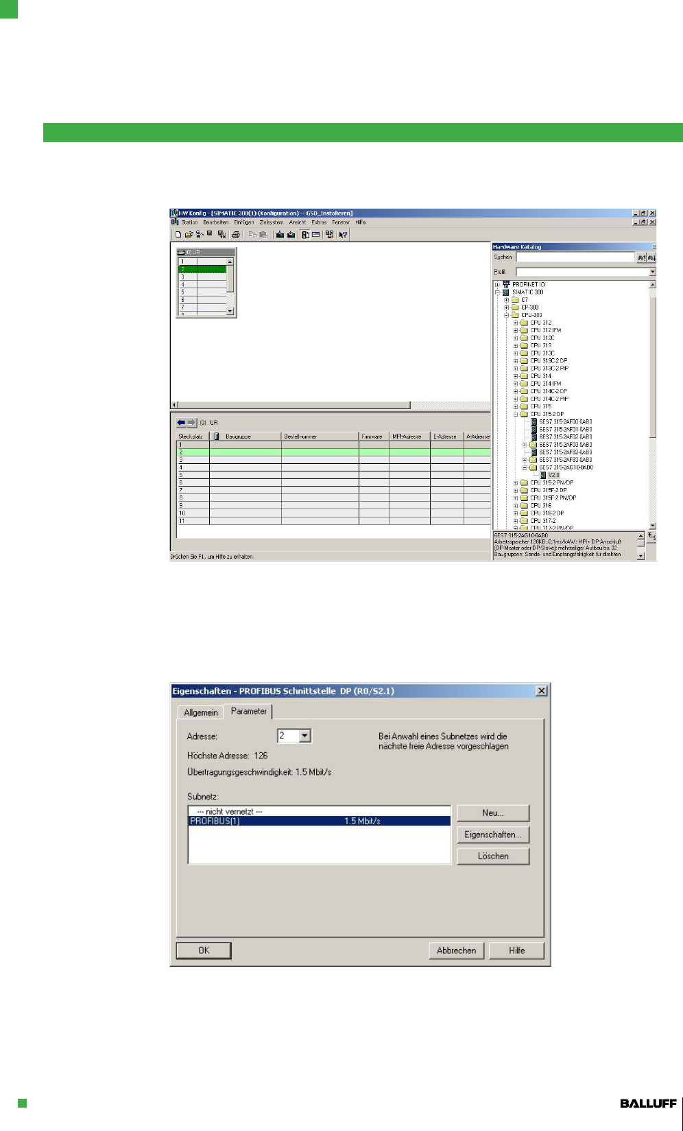
Selecting the
module
Fig. 23: The modules are shown in the product tree.
To be able to select a CPU, you must first have selected a module carrier, here for example
“RACK-300”.
In the hardware catalog under “SIMATIC 300” select | “RACK-300 | Rail”.
Fig. 24: Selecting a module
►
Startup
9
BIS L-409 IO-Link Device
Processor
www.balluff.com 37
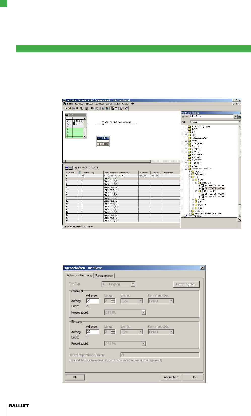
Selecting the
CPU
Specifying the
properties
Select CPU from the hardware catalog.
Fig. 25: Selecting CPU
Double-click to open the properties.
The “Properties - PROFIBUS Interface DP” opens.
Specify the Profibus address of the CPU and select subnet “PROFIBUS”.
Fig. 26: Specifying CPU properties
►
►
⇒
►
Startup
9
BIS L-409 IO-Link Device
Processor
38
Add DP slave
(IO-Link Master)
Specifying
the address
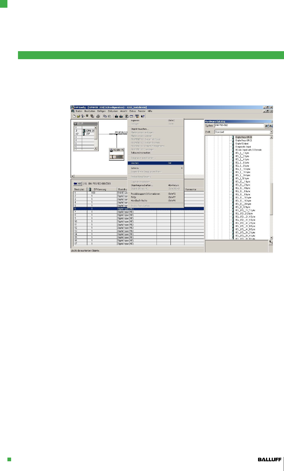
The modules are located in the hardware catalog under “Other field devices”.
The IO-Link Master is added as a DP slave:
Select Profibus rail.
Add IO-Link Master as DP-Slave by double-clicking.
The slots are assigned the default settings.
Fig. 27: Adding a module as a DP slave
Double-click on the head module to open the properties.
The “Properties - DP-Slave” window opens.
Specify addressing of the head module.
Fig. 28: Specifying addressing of the head module
►
►
⇒
►
⇒
►
Startup
9
BIS L-409 IO-Link Device
Processor
www.balluff.com 39
Configuring
inputs or outputs
The ports and PINs are represented by the slots.
In the example an IO-Link port is configured.
Select Slot 6.
Select the menu command “Edit | Delete”.
Fig. 29: Slot 6 selected, deleting default setting
►
►
Startup
9
BIS L-409 IO-Link Device
Processor
40
Add device
After deleting the default setting:
Port and PIN are displayed.
Fig. 30: Slot for port and PIN is free
The IO-Link slot can now be assigned the data module “IOL_I/O_8/8_Byte”, which is used for
the BIS L-409-....
Use drag and drop to assign the data module to the free slot.
Fig. 31: Using drag and drop to assign the data module to the free slot.
⇒
►
Startup
9
BIS L-409 IO-Link Device
Processor
www.balluff.com 41
10.1 Function
principle
10.2 Operating mode
The BIS L-409-... Identification System is a non-contact read-only system. The compact proces-
sor consists of processing circuitry with a fixed read head.
The system may be used to read information which has been permanently programmed into the
data carrier and to send current status messages to the controller.
The main components of the BIS L-409-... Identification System are:
Processor,
read head,
data carriers.
A
Fig. 32: Schematic representation of an identification system
The data carrier is an autonomous unit which is supplied with power by the read head. The read
head continuously sends a carrier signal which is picked up by the data carrier from within a
certain distance. Once the data carrier is powered, a static read operation takes place.
The processor manages the data transfer between read head and data carrier, serves as a buffer
storage device, and sends the data to the host controller.
The data are passed to the IO-Link Master using IO-Link protocol, and the Master then passes
them to the controlling system.
Host systems may be the following:
A control computer (e.g. industrial PC),
a PLC.
The BIS L-409-... supports cyclical data exchange via IO-Link protocol and standard IO mode.
Recognition of a data carrier (Codetag Present, 24 V) or no data carrier (0 V) is sent on the data
line C/Q as a digital switching signal.
In cyclical data exchange the BIS L-409-... cyclically sends read data to the controller. It is also
possible to read or enter parameter data in this mode.
–
–
–
–
–
Device Function
10
Data carrier BIS L-2…
Connection to
IO-Link Master
BIS L-409 IO-Link Device
Processor
42
10.3 Process data
Output/Input
buffer
The start addresses of the input and output data are assigned in the hardware configuration for
the host system. The BIS L-409-... uses 8 bytes of input and 8 bytes of output data, with assign-
ment as described in the following. Subaddress 00hex corresponds to the respective start
address of the hardware configuration.
The BIS L-409-... provides two fields for sending commands and data between the BIS L-409…
and the host system:
Output buffer
Input buffer
These fields are embedded into the process data transmission via the IO-Link Master. As
described above, 8 bytes of process data are sent in each direction.
The map of this process data is described below:
Output buffer:
Bit-No.
Subaddress
7 6 5 4 3 2 1 0
00hex - 1st bit header KA GR
01hex
02hex
03hex
04hex
05hex
06hex
07hex - 2nd bit
header
KA GR
Explanations for output buffer:
Subad-
dress
Bit
name
Meaning Function description
00hex 1st bit header
KA Head on/off 1
0
=
=
Head off (read head turned off)
Head on (read head operating)
GR Ground state 1
0
=
=
Software-Reset - causes the BIS to go to the
ground state
Normal operation
07hex 2. bit header
KA, GR If 1st and 2nd bit headers agree, there are valid
commands
–
–
Device Function
10
BIS L-409 IO-Link Device
Processor
www.balluff.com 43
Input buffer:
Bit-No.
Subaddress
76543210
00hex - 1st bit header BB HF AF CP
01hex Error code or data (LOWBYTE)
02hex Data
03hex Data
04hex Data or CRC_16
05hex Data (HIGHBYTE) or CRC_16
06hex not used
07hex - 2nd bit header BB HF AF CP
Explanations for input buffer:
Subad-
dress
Bit
name
Meaning Function description
00hex 1st bit header
BB Power 1
0
=
=
Device is ready
Device is in ground state
HF Head Failure 1
0
=
=
Head is turned off
Head is turned on
AF Job error 1
0
=
=
Job incorrectly processed
Job processed without error
CP Codetag Present 1
0
=
=
Data carrier is within range of the head
No data carrier in range
01hex Error code Error number is entered if the job was incorrectly
processed or canceled.
Only valid with AF bit!
0Ehex = The CRC on the data carrier does not
agree with the calculated CRC for the read data.
0Fhex = 1st and 2nd bit header of the output buffer
do not agree.
or: Data Data which were read from the data carrier
02hex Data Data which were read from the data carrier
03hex Data Data which were read from the data carrier
04hex Data Data which were read from the data carrier
or: CRC CRC read from the data carrier
05hex Data Data which were read from the data carrier
or: CRC CRC read from the data carrier
06hex - not used
07hex 2. bit header
BB, HF, AF, CP If 1st and 2nd bit headers agree, there are valid
data
Note
The 1st and 2nd header must be compared by the user (host system) in order to
query the validity of the sent data.
Device Function
10
BIS L-409 IO-Link Device
Processor
44
When communication is initiated by the IO-Link Master, transmission of the current process data
begins. Reading is automatic and does not have to be initiated.
The bit headers of the output buffer offer the possibility of having the device go into the ground
state or to turn off a head. For this the corresponding control commands in the two bit headers
need to be set (see “Process data” on page 42). If the bits are cleared again, the module
resumes operation.
The processor sends the current process data in each cycle. The data are only valid if the two bit
headers agree. The bit headers show the status of the device and the subaddress 01hex … 05hex
contains data.
If an error occurs (AF bit =1), an error code is sent in subaddress 01hex (see “Process data” on
page 42).
If no data carrier is present (CP bit = 0), the stored data from the last data carrier are displayed
until a new data carrier enters the active zone of the head. The stored data can be deleted with a
reset by setting the GR bit.
The following examples show the protocol sequence in various situations.
Device started, no data carrier yet present:
Command from controller Response from BIS L-409
1. Process output buffer: 2. Process input buffer:
00hex GR bit = 0, KA bit = 0 00hex Set BB bit
07hex GR bit = 0, KA bit = 0 01 ... 02hex Software Revision
e.g. 01hex00hex = V 1.00
07hex Set BB bit
Device start if data carrier present or
Read a data carrier in the active zone:
Command from controller Response from BIS L-409
1. Process output buffer: 2. Process input buffer:
00hex GR bit = 0, KA bit = 0 00hex Set CP bit
07hex GR bit = 0, KA bit = 0 01 ... 05hex 5 bytes of data
07hex Set CP bit
No data carrier in range:
Command from controller Response from BIS L-409
1. Process output buffer: 2. Process input buffer:
00hex GR bit = 0, KA bit = 0 00hex Clear CP bit
07hex GR bit = 0, KA bit = 0 01 ... 05hex 5 bytes of data (stored, last
current data)
07hex Clear CP bit
10.4 Protocol
sequence
10.5 Protocol
examples
1st example
2nd example
3rd example
Device Function
10
BIS L-409 IO-Link Device
Processor
www.balluff.com 45
4th example
5th example
Job incorrectly processed:
Command from controller Response from BIS L-409
Process input buffer:
00hex Set AF bit
01hex Error code (1 byte)
02 ... 05hex 4 bytes of data (stored, last
current data)
07hex Set AF bit
Turn off read head:
Command from controller Response from BIS L-409
1. Process output buffer: 2. Process input buffer:
00hex KA bit = 1 00hex Set HF bit and clear CP bit
07hex KA bit = 1 01 ... 05hex 5 bytes of data (stored, last
current data)
07hex Set HF bit and clear CP bit
New data carrier in range:
3. Process output buffer: 4. Turn off head and process input buffer:
00hex KA bit = 1 00hex Set HF bit and clear CP bit
07hex KA bit = 1 01 ... 05hex 5 bytes of data (stored, last
current data)
07hex Set HF bit and clear CP bit
Turn on read head:
5. Process output buffer: 6. Turn on head and process input buffer:
00hex KA bit = 0 00hex Clear HF bit
07hex KA bit = 0 01 ... 05hex 5 bytes of data (updated data
for the new data carrier)
07hex Clear HF bit
Device Function
10
BIS L-409 IO-Link Device
Processor

46
Device Function
10
6th example
10.6 Error codes
Place device in ground state:
Command from controller Response from BIS L-409
1. Process output buffer: 2. Go to ground state and process input
buffer:
00hex GR bit = 1 00hex Clear BB bit
07hex GR bit = 1 01...05hex each 00hex
07hex Clear BB bit
3. Process output buffer: 4. Start running and process input buffer:1)
00hex GR bit = 0 00hex Set BB bit
07hex GR bit = 0 01...05hex 5 bytes of data
07hex Set BB bit
1) If there is no data carrier in range, the
input buffer is filled with 00hex.
Error code Meaning Remedy
0Ehex CRC error Data carrier was not successfully read.
Possible causes:
Data carrier defective
Transmission failed
Data carrier not CRC capable
–
–
–
0Fhex Format error The two headers in the output buffer and in the host
system do not agree.
The headers must be matched (see “Output buffer”
page 42).
BIS L-409 IO-Link Device
Processor
www.balluff.com 47
Device Function
10
10.7 Data
transmission
timing
Fig. 33: Timing of data carrier recognition and data transmission
1 Data carrier in range
2 Data carrier recognized (Tag-Present LED,
Codetag-Present bit)
t1 Data read time
t2 Polling time
t3 Cycle time
In-Data: Input data
Out-Data: Output data
Process-Data-Cycle: Process data cycle
Byte a+b: Process data
x: Data required
Data read time t1:
Time until the data from a data carrier entering the read range are actually read. The read time is:
70 ms × number of parameterized data compare counts, Default = 2 (see “Map of parameter-
izing data” on page 33).
Polling time t2:
Time until it is recognized that the data carrier is no longer in the read range (polling time). The
polling time is 50 ms.
Cycle time t3:
Time between the sending of two frames. The cycle time depends on the set baud rate and the
respective Master (see “Direct Parameter Page” on page 30)
In-Data/Out-Data:
Sending of the input data and output data. 8 frames of 2 bytes each are sent, alternating pro-
cess data and required data (x).
Process Data Cycle:
A process data cycle consists of the complete sending of the input and output data. At the
beginning of each process data cycle the current data are polled and immediately sent.
BIS L-409 IO-Link Device
Processor

48
Device Function
10
Updating the IO-
Link Master data
When a data carrier enters the read range, its data are read and stored within time t1. The data
are sent at the next start of a process data cycle (In-Data).
The data carrier should be located within the read range at the start of a process data cycle so
that the CP bit is set when the current data are polled. If the data carrier leaves the read range
before polling, the data are sent but the CP bit is not set. If the dwell time of a data carrier in the
read range is very short and if another data carrier immediately arrives, loss of data may result in
the worst case.
The minimum time until the most current data are available on the IO-Link Master is 16×t3. The
time corresponds to the sending time of 16 frames or one process data cycle with the param-
eterized cycle time (depending on the set baud rate and the host Master, see also “Direct
Parameter Page” on page 30).
BIS L-409 IO-Link Device
Processor

www.balluff.com 49
Ordering code
Accessories
(optional, not
included)
Appendix
BIS L-409 IO-Link Device
Processor
BIS L – 409 – 045 – 00X –07– S4
Balluff Identification System
Series
L = Read system
Hardware type
409 = Plastic housing, IO-Link
Software type
045 = Software number, IO-Link
Version
001 = Coil Ø 34 mm
002 = Offset read head M18 (0.5 m cable)
003 = Offset read head M12 (0.5 m cable)
004 = Remote read head C-305 housing (0.5 m cable)
Interface
07 = IO-Link
Mod-
ule
S4 = M12 4-pin male
Accessories for the BIS L-409-... can be found in the Balluff IO-Link catalog.
The catalog can be downloaded on the Internet at “www.balluff.de”.
50
Decimal Hex Control
Code
ASCII Decimal Hex ASCII Decimal Hex ASCII
0 00 Ctrl @ NUL 43 2B + 86 56 V
1 01 Ctrl A SOH 44 2C , 87 57 W
2 02 Ctrl B STX 45 2D - 88 58 X
3 03 Ctrl C ETX 46 2E . 89 59 Y
4 04 Ctrl D EOT 47 2F / 90 5 A Z
5 05 Ctrl E ENQ 48 30 0 91 5B [
6 06 Ctrl F ACK 49 31 1 92 5C \
7 07 Ctrl G BEL 50 32 2 93 5D [
8 08 Ctrl H BS 51 33 3 94 5E ^
9 09 Ctrl I HT 52 34 4 95 5F _
10 0 A Ctrl J LF 53 35 5 96 60 `
11 0B Ctrl K VT 54 36 6 97 61 A
12 0C Ctrl L FF 55 37 7 98 62 B
13 0D Ctrl M CR 56 38 8 99 63 c
14 0E Ctrl N SO 57 39 9 100 64 d
15 0F Ctrl O SI 58 3 A : 101 65 e
16 10 Ctrl P DLE 59 3B ; 102 66 f
17 11 Ctrl Q DC1 60 3C < 103 67 g
18 12 Ctrl R DC2 61 3D = 104 68 h
19 13 Ctrl S DC3 62 3E > 105 69 i
20 14 Ctrl T DC4 63 3F ? 106 6 A j
21 15 Ctrl U NAK 64 40 @ 107 6B k
22 16 Ctrl V SYN 65 41 A 108 6C L
23 17 Ctrl W ETB 66 42 B 109 6D m
24 18 Ctrl X CAN 67 43 C 110 6E n
25 19 Ctrl Y EM 68 44 D 111 6F o
26 1 A Ctrl Z SUB 69 45 E 112 70 p
27 1B Ctrl [ ESC 70 46 F 113 71 q
28 1C Ctrl \ FS 71 47 G 114 72 r
29 1D Ctrl ] GS 72 48 H 115 73 s
30 1E Ctrl ^ RS 73 49 I 116 74 t
31 1F Ctrl _ US 74 4 A J 117 75 u
32 20 SP 75 4B K 118 76 V
33 21 ! 76 4C L 119 77 W
34 22 " 77 4D M 120 78 X
35 23 # 78 4E N 121 79 Y
36 24 $ 79 4F O 122 7 A Z
37 25 % 80 50 P 123 7B {
38 26 & 81 51 Q 124 7C |
39 27 ‘ 82 52 R 125 7D }
40 28 ( 83 53 S 126 7E ~
41 29 ) 84 54 T 127 7F DEL
42 2 A * 85 55 U
ASCII table
Appendix
BIS L-409 IO-Link Device
Processor

www.balluff.com 51
A
Accessories 49
ASCII table 50
C
Characteristic data 16, 18, 20, 22
Checksum 33
Connections 11, 12, 27, 28
CRC check 33
Error message 41
D
Data carrier 33
Data comparison counter 34
Data integrity 15
CRC_16 data check 15
Double reading 15
Data modules 35
Dimensions 16, 18, 20, 22
Distance between processors 26
E
Electrical Data 17, 19, 21, 23
Error codes 43, 46
F
Functional principle 13
Function indicators 17, 19, 21, 23
Function principle 41
G
GSD file 35
H
Hardware settings 28
I
Installation 24
Installing the GSD file 35
Integration 35
GSD file, head module,
data modules 35
Intended use 7
IO-Link connection 28
M
Mechanical data 16, 18, 20, 22
O
Operating conditions 17, 19, 21, 23
Operating mode 41
Orienting the read head 27
Output/Input buffer 42
P
Part Numbering 49
Process data 42
Processor
Data integrity 15
Function principle 41
Parameter data 32
Product description 15
Product description 15
Project planning software 35
Protocol examples 44
Protocol sequence 44
S
Safety 7
Installation 7
Operation 7
Startup 7
T
Technical data
Characteristic data 16, 18, 20, 22
Dimensions 16, 18, 20, 22
Electrical Data 17, 19, 21, 23
Function indicators 17, 19, 21, 23
Mechanical data 16, 18, 20, 22
Operating conditions 17, 19, 21, 23
Appendix
BIS L-409 IO-Link Device
Processor

Balluff GmbH
Schurwaldstrasse 9
73765 Neuhausen a.d.F.
Germany
Phone +49 7158 173-0
Fax +49 7158 5010
balluff@balluff.de
No. 858282 . 00.000000 . Edition 0804; Subject to modification.
www.balluff.com
www.balluff.com